Embed Size (px)
Citation preview
TCAD Challenges in the Nanotechnology Era
Martin D. Giles
Technology CAD, Design & Technology Solutions, Intel Corporation RA3-254, 2501 NW 229th Avenue, Hillsboro, OR 95124, USA
E-mail: [email protected]
Abstract – TCAD process and device modeling has become an essential component of advanced technology development, delivering physical insight into processes and device operation and enabling development and optimization of technology flows. This paper highlights emerging challenges in extending these capabilities into the nanotechnology era, and the opportunities for a hierarchical, physically-based modeling approach to impact the direction of nanotechnology development.
I. INTRODUCTION
Technology computer-aided design (TCAD) is now an accepted part of modern technology development. From its early beginnings in 1D device and process modeling, TCAD now addresses almost every aspect of semiconductor technology development from equipment and lithography modeling through process and device modeling to compact device modeling as the interface to the circuit design world. Modeling is essential to achieving technology development goals, both in increasing device density and performance as well as delivering a technology with high yield and manufacturability.
The nanotechnology era brings challenges to all aspects of technology development, and correspondingly to all areas of TCAD. However, a key focus for nanotechnology development is to find ways to improve intrinsic device performance to keep on the improvement trend that has characterized the semiconductor industry for the past 40 years. This paper focuses on the emerging challenges for process and device TCAD that will be required to enable that continuing performance gain.
II. ENTERING THE NANOTECHNOLOGY ERA
Nanotechnology has been defined as research and technology development at the atomic, molecular or macromolecular levels in the length scale of approximately 1-100 nm [1]. By this measure the semiconductor industry entered the nanotechnology era in 2003 when the first volume production of 90nm technology began [2]. The previous decade of CMOS transistor technology development was characterized by a focus on gate oxide scaling coupled with dopant diffusion/activation engineering to achieve good electrostatic control of the
channel with low external resistance as devices were scaled. The introduction of strained silicon at 90nm began a focus on channel mobility engineering as a key component of technology scaling and an increase in the pace of introduction of new materials and structures to achieve technology development goals. This increased pace of change presents new challenges and new opportunities for TCAD to impact technology development. Nanotechnology also brings the possibility of leveraging new physical phenomena in highly confined structures to improve performance or even change the operating principles of the devices we use.
For front-end process simulation, the main focus of the past decade has been on understanding and controlling dopant diffusion and activation to enable junction scaling and channel engineering. The replacement of local oxidation with shallow trench isolation for the 0.35µm generation in 1994 [3] left ion implantation and diffusion as the most critical processing steps. Detailed physical modeling of damage formation during ion implantation, dopant-defect clustering in the early stages of annealing, and subsequent cluster dissolution and transient enhanced diffusion, were essential to understand the annealing behavior. Continuum diffusion modeling approaches remained the standard for industrial technology development, but with increasingly detailed descriptions of the reaction-diffusion systems underlying macroscopic dopant diffusion and activation behavior. Similarly on the device side, continuum drift-diffusion transport modeling has remained the standard workhorse for technology development. Insights from more advanced transport models such as Energy Balance and Monte Carlo, and quantum effects from Schrödinger-Poisson solutions, have been incorporated into the drift-diffusion framework through effective mobility and quantum correction terms.
Looking ahead in nanotechnology, three regimes of technology development and their related modeling needs have been identified [4]. Evolutionary CMOS pushes silicon scaling to the limit, incorporating new materials, processes, and geometries to achieve power and performance goals while continuing to use silicon as the channel transport material. It includes advances such as high-k/metal gate, strained silicon, FinFET and Tri-gate device architectures. Process/device TCAD can guide technology development efforts to use these new features to continue scale device size while decreasing power and
7
1-2(Plenary)
improving performance. Revolutionary CMOS goes beyond silicon to push charge-based transport to its ultimate limits including new channel materials such as Germanium and III-V semiconductors on silicon, nanowires, and carbon nanotube-based FETs. These technologies are further in the future, but TCAD has a role now in enabling a detailed evaluation of the strengths and limitations of these possible successors to silicon and in complementing experimental studies of their transport properties. Even further in the future, Exotic Technologies goes beyond charge-based devices to consider other forms of state variable such as spintronics and photonics. These devices are far from practical realization for industrial applications, yet modeling can contribute to determining the feasibility and potential benefits of these alternatives.
Meeting these nanotechnology modeling challenges will require a hierarchical approach that can span the diverse range of length and time scales involved, built on a foundation of atomic scale physical modeling of process technology and device operation, and reaching up into the circuit and systems level [5]. The next sections will consider the specific challenges of the process and device modeling areas, progress made so far, and the challenges ahead.
III. PROCESS MODELING CHALLENGES
Current technology needs have driven the development of detailed physical models for dopant implantation and diffusion effects [6]. Careful experiments targeted at understanding basic physical mechanisms such as dopant-defect clustering and extended defect formation and dissolution have enabled the development of continuum reaction-diffusion models that can then be applied for technology understanding. For example, transient enhanced diffusion (TED) from ion implantation damage was found to limit junction scaling as annealing temperatures were reduced. Transmission electron microscopy studies coupled with diffusion experiments in MBE-grown superlattices [7] led to an understanding of the controlling role of {311} extended defects in setting the timescale of TED and guided formulation of appropriate models. Atomistic modeling approaches have also been developed by several groups using ab initio calculations of formation and migration energies to feed into continuum models for dopants and defects [8,9,10]. These calculation methods have reached a point where they are beginning to provide predictive input to important technology questions such as the influence of local stress on boron diffusion and activation [11,12].
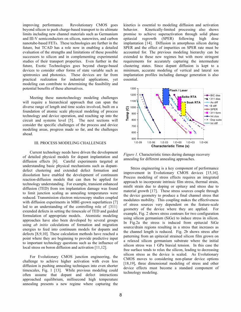
For Evolutionary CMOS junction engineering, the challenge to achieve higher activation with even less diffusion is pushing annealing techniques into even shorter timescales, Fig. 1 [13]. While previous modeling could often assume that dopant and defect interactions approached equilibrium, millisecond high temperature annealing presents a new regime where capturing the
kinetics is essential to modeling diffusion and activation behavior. Kinetically-limited processing also shows promise to achieve superactivation through solid phase epitaxial regrowth (SPER) following high dose implantation [14]. Diffusion in amorphous silicon during SPER and the effect of impurities on SPER rate must be accounted for. The previous modeling hierarchy can be extended to these new regimes but with more stringent requirements for accurately capturing the intermediate clustering states. Since dopant diffusion is kept to a minimum, accurate modeling of vertical and lateral ion implantation profiles including damage generation is also essential.
Figure 1. Characteristic times during damage recovery annealing for different annealing approaches.
500
600
700
800
900
1000
1100
1200
1300
1.E-09 1.E-06 1.E-03 1.E+00 1.E+03 1.E+06Characteristic Time (s)
Tem
p (C
)
BIC diss311 dissAs diffB diffSPER 311 formInt clusDop subsInt diff
Flash / Laser
Spike RTA
Soak RTA
Stress engineering is a key component of performance improvement in Evolutionary CMOS devices [15,16]. Process modeling of stress effects requires an integrated approach to incorporate intrinsic film stress, thermal strain, misfit strain due to doping or epitaxy and stress due to material growth [17]. These stress sources couple through the device geometry to produce a final channel stress that modulates mobility. This coupling makes the effectiveness of stress sources very dependent on the feature-scale geometry of the device where they are applied. For example, Fig. 2 shows stress contours for two configuration using silicon germanium (SiGe) to induce stress in silicon. In Fig.2a the stress is induced from epitaxial SiGe source/drain regions resulting in a stress that increases as the channel length is reduced. Fig. 2b shows stress after patterning from an epitaxial strained silicon film grown on a relaxed silicon germanium substrate where the initial silicon stress was 1 GPa biaxial tension. In this case the free surface tends to relax the silicon, leading to decreasing silicon stress as the device is scaled. As Evolutionary CMOS moves to considering non-planar device options [18,19], three dimensional modeling of stress and other device effects must become a standard component of technology modeling.
8

Figure 2. (a) Stress contours (MPa) along the channel direction [110] in a short channel PMOS device, (b) Stress contours of strained Si on relaxed SiGe after etching
Pushing to the limits of Evolutionary CMOS is calling for the introduction of new dielectric and gate electrode materials to enable continued electrical scaling of the gate stack. The resulting electrical properties are very sensitive to the choice of materials, thicknesses of interfacial layers, and thermal processing history [20]. Modeling can help understanding these tradeoffs, such as the impact of metal vs. polysilicon gate and interfacial oxide thickness on channel mobility [21]. Experimental determination of detailed interface structure is very challenging but by combining ab initio modeling with high resolution TEM imaging and electron energy loss spectroscopy [22,23], atomic structure information is beginning to be determined with the potential to provide detailed surface structure and electronic state description for mobility modeling.
Modeling of high-k dielectric materials and interface properties is only the next step in an increasing requirement to develop computational material science capabilities to enable modeling beyond silicon for Revolutionary CMOS technologies. While the progress in silicon-related work is
encouraging, much remains to be done to move computational materials modeling from the specialized research environment into more routine industrial application supporting modeling of new materials. Dopant diffusion and activation processes in Germanium and in III-V semiconductors have been studied, but not at the level of detail required for nanoscale device development. Stress effects are intrinsic to multilayer heterostructure devices and will be an integral part of device performance engineering. Forming a well behaved dielectric interface is the key obstacle in creating MOS devices beyond silicon. In addition to these traditional TCAD process modeling challenges, Revolutionary CMOS device options include semiconductor nanowires and carbon nanotubes where the challenges of reliable die scale formation and assembly are even greater than the challenges of the individual devices. The combination of targeted experiments and detailed physical modeling that has proven successful in the silicon domain must be extended to these new materials systems and better approaches developed to allow us to effectively explore the large configuration space of realistic bulk and interface structures.
(a)
(b)
SiGe Silicon
Silicon IV. DEVICE MODELING CHALLENGES
Drift-diffusion device modeling using empirically calibrated mobility models has been remarkably successful at meeting mainstream device modeling needs for many technology generations. However, we have now entered a new phase even in Evolutionary CMOS development where new materials and structures are required to continue to scale devices. Physically-based modeling of nanoscale device operation and how it relates to materials and interface structure is essential to support technology development efforts.
SiGe
The introduction of strained silicon into mainstream technology at the 90nm node began a new focus on channel mobility engineering. Although the piezoresistance effect in silicon has been known for 50 years and biaxial tensile strained silicon investigated for more than a decade, the large mobility gains possible with dominantly uniaxially strain quickly raised the importance of fundamental device stress understanding for arbitrary stress configurations, particularly for PMOS. Earlier work on hole mobility under biaxial stress used a k.p quantum model to investigate the physics of mobility enhancement [24]. This approach has been applied for arbitrary stress including anisotropic scattering [25] and combined with full-band Monte Carlo transport modeling using an arbitrary stress tensor bandstructure [26]. Fig. 3 shows energy contours of the lowest energy hole band under uniaxial stress in a typical device configuration. Stress and gate field both modulate the band structure, changing local curvature and reducing scattering. However, for this uniaxial stress configuration, repopulation within the band due to warping is the most significant effect [16]. Holes move from the
9

A,B wings to the lower energy C,D wings where they have lower effective mass along the [110] channel transport direction. In contrast, biaxial stress benefits from scattering reduction but does not see in-plane repopulation so is not as effective in improving hole mobility, Fig. 4 [25].
Figure 3. First subband energy contours under 1GPa uniaxial stress along the [110] direction, with an effective field of 1MV/cm (30meV per contour). Simulation shows that the C and D wings have reduced energy.
Figure 4. Hole mobility vs. effective field for different stress configurations.
The same basic calculation approach – the study of bandstructure, carrier population, and scattering rates – has proved valuable in studying several other device transport effects. Channel mobility degradation from high-k dielectrics on silicon has been understood as the consequence of remote surface optical (SO) phonon scattering [27], and the beneficial effect of a metal gate screening optical phonon modes demonstrated [21]. Moving to Revolutionary CMOS devices, similar calculations have enabled the early assessment of phonon-
limited mobility in silicon nanowires where increased electron-phonon overlap produces increased scattering despite the transition to a 1D bandstructure [28]. These kinds of assessments are a valuable complement to early experimental studies of novel devices that are often confounded by measurement limitations and parasitic effects. Refining these calculations with a more detailed treatment of the finite system bandstructure, effect of surface states, and modeling of the confined phonon spectrum will enable tradeoffs in novel device design and performance to be better understood. For highly scaled devices, quantum effects along the transport direction must also be considered using an approach such as non-equilibrium Green’s function [29,30].
A C
k y (2π/
a)
In addition to bringing the potential of improved charge transport, scaling through the Nanoscale era brings new challenges in dealing with device variation and with power dissipation. At these very small dimensions, structural features are below the phonon mean free path and classical treatments for continuum heat transport no longer apply. A hierarchical approach can be used to link quantum/atomistic phonon descriptions to device scale behavior [31] to understand local heating effects. The phonon distribution must then be linked back to the device transport calculation for a fully-consistent picture of non-equilibrium thermal effects.
B D
kx (2π/a)
The need for hierarchical modeling from atoms to device properties also extends up to the circuit level so that the circuit consequences of device characteristics can be evaluated. Scaling Evolutionary CMOS increases sensitivity to device variation because the active device volume becomes so small. Capturing this at the design level will require building stronger coupling down through the hierarchy to the material or even atomic level. The novel device options of Revolutionary CMOS will lead to quite different circuit design approaches. Fully exploiting their potential will require breaking the traditional boundaries to understand, for example, new system options from Revolutionary CMOS materials and device behavior.
VI. CONCLUSION
TCAD process and device modeling has become an essential component of advanced technology development, delivering physical insight into processes and device operation and enabling development and optimization of technology flows. Moving into the nanotechnology era, the demands on model-based understanding will only increase. Meeting the rapidly advancing challenge of new materials and device structures requires a physically-based, hierarchical modeling approach. The work highlighted here shows that building from atoms to materials to devices can deliver the understanding that technology development requires and has the potential to reach even further up the hierarchy to enable circuit and system level tradeoffs.
0
100
200
300
400
500
0 0.2 0.4 0.6 0.8 1Effective Field (MV/cm)
Mob
ility
(cm
2/Vs
)
No Stress1GPa Bi-comp1GPa Uni-comp2GPa Bi-tensile
10
ACKNOWLEDGEMENTS
The author gratefully acknowledges the many contributions to the work presented here by members of the Intel TCAD process/device modeling group, including S.Cea, H.Kennel, P.Keys, R.Kotlyar, A.Lilak, T.Linton, P.Matagne, B.Obradovic, R.Shaheed, L.Shifren, M.Stettler, C.Weber, and X.Wang, and by members of the Intel Portland Technology Development and Portland Quality and Reliability organizations.
REFERENCES
[1] “National Nanotechnology Initiative: Leading to the
Next Industrial Revolution,” National Science and Technology Council Report, February 2000.
[2] T. Ghani, M. Armstrong, C. Auth, M. Bost, P. Charavat, G. Glass, T. Hoffmann, K. Johnson, C. Kenyon, J. Klaus, B. McIntyre, K. Mistry, A. Murthy, J. Sandford, M. Silberstein, S. Sivakumar, P. Smith, K. Zawadzki, S. Thompson, M. Bohr, “A 90nm high volume manufacturing logic technology featuring novel 45nm gate length strained silicon CMOS transistors,” 2003 IEEE International Electron Devices Meeting Proceedings, p. 978.
[3] M. Bohr, S. U. Ahmed, L. Brigham, R. Chau, R. Gasser, R. Green, W. Hargrove, E. Lee, R. Natter, S. Thompson, K. Weldon, S. Yang, “A high performance 0.3µm logic technology for 3.3V and 2.5V operation,” 1994 IEEE International Electron Devices Meeting Proceedings, p.273.
[4] M.D. Giles, “TCAD process/device modeling challenges and opportunities for the next decade,” Journal of Computational Electronics, in press.
[5] M. Giles, H. Hosack, W. Joyner, G. Klimeck, M. Lundstrom, C. Musgrave, V. Varadan, “Multi-scale, multi-phenomena modeling and simulation,” National Nanotechnology Initiative Consultative Working Group 3 Report, Silicon Nanoelectronics and Beyond, August 2004.
[6] H. W. Kennel, S. M .Cea, A. D. Lilak, P. H. Keys, M. D. Giles, J. Hwang, J. S. Sandford, S. Corcoran, “Modeling of ultrahighly doped shallow junctions for aggressively scaled CMOS,” 2002 IEEE International Electron Devices Meeting Proceedings, p.875.
[7] D. J. Eaglesham, P. A. Stolk, H. –J. Gossmann, J. M. Poate, “Implantation and transient B diffusion in Si: the source of the interstitials,” Appl. Phys. Lett. 65 (18), 2305 (1994).
[8] S. K. Theiss, M. J. Caturla, M. D. Johnson, J. Zhu, T. Lenosky, B. Sadigh, T. Diaz de la Rubia, “Atomic scale models of ion implantation and dopant diffusion in silicon,” Thin Solid Films 365, 219 (2000).
[9] L. Pelaz, M. Aboy, L. Marques, P. Lopez, I. Santos, “Atomistic modeling of junction formation in Si,” Eighth International Workshop on Fabrication,
Characterization, and Modeling of Ultra-Shallow Doping Profiles in Semiconductors, p.211 (2005).
[10] W. Windl, R. Stumpf, X. -Y. Liu, M. P. Masquelier, “Ab initio modeling study of boron diffusion in silicon,” Comp. Mat. Sci. 21, 496 (2001).
[11] M. Diebel, S. T. Dunham, “Ab-initio calculations to predict stress effects on defects and diffusion in silicon,” 2003 IEEE International Conference on Simulation of Semiconductor Processes and Devices, p. 1474
[12] M. Diebel, S. Chakravarthi, S. T. Dunham, C. F. Machala, “Ab-initio calculations to predict stress effects on boron solubility in silicon,” Simulation of Semiconductor Processes and Devices 2004, p.37, Springer-Verlag 2004.
[13] H.W. Kennel, P.H. Keys, M. Armstrong, A. Budrevich, M.D. Giles, M. Liu, “Activating challow junctions: Insight from modeling,” Eighth International Workshop on Fabrication, Characterization, and Modeling of Ultra-Shallow Doping Profiles in Semiconductors, p.211 (2005).
[14] S.H. Jain, P.B. Griffin, J.D. Plummer, S. McCoy, J.Gelpey, T. Selinger, D.F. Downey, “Metastable boron active concentrations in Si using flash assisted solid phase epitaxy,” J. Appl. Phys. 96 (12), p.7357 (2004).
[15] K. Mistry, M. Armstrong, C. Auth, S. Cea, T. Coan, T. Ghani, T. Hoffmann, A. Murthy, J. Sandford, R. Shaheed, K. Zawadzki, K. Zhang, S. Thompson, M. Bohr, “Delaying forever: Uniaxial strained silicon transistors in a 90nm CMOS technology,” Symp. VLSI Tech., p.50 (2004).
[16] M. D. Giles, M. Armstrong, C. Auth, S. M. Cea, T. Ghani, T. Hoffmann, R. Kotlyar, P. Matagne, K. Mistry, R. Nagisetty, B. Obradovic, R. Shaheed, L. Shifren, M. Stettler, S. Tyagi, X. Wang, C. Weber, K. Zawadzki, “Understanding stress enhanced performance in Intel 90nm CMOS technology,” Symp. VLSI Tech., p.118 (2004).
[17] S. M. Cea, M. Armstrong, C. Auth, T. Ghani, M. D. Giles, T. Hoffmann, R. Kotlyar, P. Matagne, K. Mistry, R. Nagisetty, B. Obradovic, R. Shaheed, L. Shifren, M. Stettler, S. Tyagi, X. Wang, C. Weber, K. Zawadzki, “Front end stress modeling for advanced logic technologies,” 2004 IEEE International Electron Devices Meeting Proceedings, p.963.
[18] G. Pei, J. Kedzierski, P. Oldiges, M. Ieong, E. Kan, “FinFET design considerations based on 3D simulation and analytical modeling,” IEEE Trans. Elec. Dev., 49 (8), p.1411 (2002).
[19] B. Doyle, B. Boyanov, S. Datta, M. Doczy, S. Hareland, B. Jin, J. Kavalieros, T. Linton, R. Rios, R. Chau, “Tri-gate fully-depleted CMOS transistors: fabrication, design, and layout,” in VLSI Symp. Tech. Dig., p.133 (2003).
[20] W. Tsai, L. -A. Ragnarsson, L. Pantisano, P. J. Chen, B. Onsia, T. Schram, E. Cartier, A. Kerber, E. Young, M. Caymax, S. De Gendt, M. Heyns, “Performance comparison of sub 1 nm sputtered TiN/HfO2 nMOS
11

and pMOSFETs,” 2003 IEEE International Electron Devices Meeting Proceedings, p. 311.
[21] R. Kotlyar, M. D. Giles, P. Matagne, B. Obradovic, L. Shifren, M. Stettler, E. Wang, “Inversion mobility and gate leakage in high-k/metal gate MOSFETs,” 2004 IEEE International Electron Devices Meeting Proceedings, p.391.
[22] W. Windl, T. Liang, S. Lopatin, G. Duscher, “Modeling and characterization of atomically sharp “perfect” Ge/SiO2 interfaces,” Mat. Sci. Eng. B114-115, p.156 (2004).
[23] T. Liang, W. Windl, S. Lopatin, G. Duscher, “Investigation of the detailed structure of atomically sharp Ge/SiO2 interfaces,” 2004 IEEE International Conference on Simulation of Semiconductor Processes and Devices, p.143 (2003).
[24] M. Fischetti, Z. Ren, P. Solomon, M. Yang, K. Rim, “Six-band k.p calculation of the hole mobility in silicon inversion layers: dependence on surface orientation, strain, and silicon thickness,” J. Appl. Phys. 94 (2), 1079 (2003).
[25] E. Wang, P. Matagne, L. Shifren, B. Obradovic, R. Kotlyar, S. Cea, J. He, Z. Ma, R. Nagisetty, S. Tyagi, M. Stettler, M. D. Giles, “Quantum mechanical calculation of hole mobility in silicon inversion layers under arbitrary stress,” 2004 IEEE International Electron Devices Meeting Proceedings, p.147.
[26] L. Shifren, X. Wang, P. Matagne, B. Obradovic, C. Auth, S. Cea, T. Ghani, J. He, T. Hoffmann, R. Kotlyar, Z. Ma, K. Mistry, R. Nagisetty, R. Shaheed, M. Stettler, C. Weber, and M.D. Giles, “Drive current enhancement in p-type metal-oxide-semiconductor field-effect transistors under shear uniaxial stress,” Appl. Phys. Lett., 85 (25), p.6188 (2004).
[27] M.V. Fischetti, D.A. Neumayer, E.A. Cartier, “Effective electron mobility in Si inversion layers in metal–oxide–semiconductor systems with a high-k insulator: The role of remote phonon scattering,” J. Appl. Phys., 90 (9) p.4587 (2001).
[28] R. Kotlyar, B. Obradovic, P. Matagne, M. Stettler, M. D. Giles, “An assessment of room temperature phonon limited mobility in gated silicon nanowires,” Appl. Phys. Lett. 84 (25), 5270 (2004).
[29] S. Datta, “The non-equilibrium Green’s function (NEGF) formalism: An elementary introduction,” 2002 IEEE International Electron Devices Meeting, p. 703.
[30] G. Klimek, “NEMO 1-D: the first NEGF-based TCAD tool,” Simulation of Semiconductor Processes and Devices 2004, p.9, Springer-Verlag 2004.
[31] E. Pop, K. E. Goodson, “Thermal phenomena in nanoscale transistors,” Ninth Intersociety Conference on Thermal and Thermomechanical Phenomena In Electronic Systems, IEEE, 2004. p. 1.
12