Embed Size (px)
Citation preview

TC648Fan Speed Controller with Auto-Shutdown
and Over-Temperature Alert
Features
• Temperature Proportional Fan Speed for Acoustic Control and Longer Fan Life
• Efficient PWM Fan Drive
• 3.0V to 5.5V Supply Range:
- Fan Voltage Independent of TC648 Supply Voltage
- Supports any Fan Voltage
• Over-temperature Fault Detection
• Automatic Shutdown Mode for “Green” Systems
• Supports Low Cost NTC/PTC Thermistors
• Space Saving 8-Pin MSOP Package
Applications
• Power Supplies
• Computers
• Portable Computers
• Telecom Equipment
• UPSs, Power Amps
• General Purpose Fan Speed Control
Available Tools
• Fan Controller Demonstration Board (TC642DEMO)
• Fan Controller Evaluation Kit (TC642EV)
Package Types
General Description
The TC648 is a switch mode, fan speed controller foruse with brushless DC fans. Temperature proportionalspeed control is accomplished using pulse width mod-ulation (PWM). A thermistor (or other voltage outputtemperature sensor) connected to the VIN inputfurnishes the required control voltage of 1.25V to 2.65V(typical) for 0% to 100% PWM duty cycle. The TC648can be configured to operate in either auto-shutdown orminimum speed mode. In auto-shutdown mode, fanoperation is automatically suspended when measuredtemperature (VIN) is lower than a user programmedminimum setting (VAS). The fan is automaticallyrestarted, and proportional speed control restored,when VIN exceeds VAS (plus hysteresis). Operation inminimum speed mode is similar to auto-shutdownmode, with the exception that the fan is operated at auser programmed minimum setting when the mea-sured temperature is low. An integrated Start-up Timerensures reliable motor start-up at turn-on, and whencoming out of shutdown or auto-shutdown mode.
The over-temperature fault output (OTF) is assertedwhen the PWM reaches 100% duty cycle, indicating apossible thermal runaway situation.
The TC648 is available in the 8-pin plastic DIP, SOICand MSOP packages and is available in the industrialand extended commercial temperature ranges.
1 8
2 7
3 6
4 5
TC648
GND
CF
VIN
VAS OTF
NC
VDD
VOUT
SOIC/PDIP/MSOP
2001-2012 Microchip Technology Inc. DS21448D-page 1

TC648
Functional Block Diagram
OTF
SHDN
NC
PWM
OTF
GND
VAS
VSHDN
VIN
CF
VDD
VOUT
TC648
ControlLogic
+
–VOTF
+
–
+
–
+
–
Start-upTimer
ClockGenerator
DS21448D-page 2 2001-2012 Microchip Technology Inc.

TC648
1.0 ELECTRICAL CHARACTERISTICS
Absolute Maximum Ratings*
Supply Voltage .........................................................6V
Input Voltage, Any Pin... (GND – 0.3V) to (VDD + 0.3V)
Package Thermal Resistance:PDIP (RJA)............................................. 125°C/WSOIC (RJA) ............................................ 155°C/WMSOP (RJA) .......................................... 200°C/W
Specified Temperature Range............ -40°C to +125°C
Storage Temperature Range.............. -65°C to +150°C
*Stresses above those listed under "Absolute Maximum Rat-ings" may cause permanent damage to the device. These arestress ratings only and functional operation of the device atthese or any other conditions above those indicated in theoperation sections of the specifications is not implied. Expo-sure to absolute maximum rating conditions for extended peri-ods may affect device reliability.
DC ELECTRICAL SPECIFICATIONS
Electrical Characteristics: Unless otherwise specified, TMIN TA TMAX, VDD = 3.0V to 5.5V
Symbol Parameter Min Typ Max Units Test Conditions
VDD Supply Voltage 3.0 — 5.5 V
IDD Supply Current, Operating — 0.5 1.0 mA Pins 6, 7 Open, CF = 1 µF, VIN = VC(MAX)
IDD(SHDN) Supply Current, Shutdown/ Auto-shutdown Mode
— 25 — µA Pins 6, 7 Open; Note 1CF =1 µF, VIN = 0.35V
IIN VIN, VAS Input Leakage -1.0 — +1.0 µA Note 1
VOUT Output
tR VOUT Rise Time — — 50 µsec IOH = 5 mA, Note 1
tF VOUT Fall Time — — 50 µsec IOL = 1 mA, Note 1
IOL Sink Current at VOUT Output 1.0 — — mA VOL = 10% of VDD
IOH Source Current at VOUT Output
5.0 — — mA VOH = 80% of VDD
SENSE Input
VTH(SENSE) SENSE Input Threshold Voltage with Respect to GND
50 70 90 mV Note 1
OTF Output
VOL Output Low Voltage — — 0.3 V IOL = 2.5 mA
VIN, VAS Inputs
VC(MAX),VOTF Voltage at VIN for 100% Duty Cycle and Overtemp. Fault
2.5 2.65 2.8 V
VC(SPAN) VC(MAX) - VC(MIN) 1.3 1.4 1.5 V
VAS Auto-shutdown Threshold VC(MAX) ~ VC(SPAN)
— VC(MAX) V
VSHDN Voltage Applied to VIN to Ensure Reset/Shutdown
— — VDD x 0.13 V
VREL Voltage Applied to VIN to Release Reset Mode
VDD x 0.19 — — V VDD = 5V
VHYST Hysteresis on VSHDN, VREL — 0.01 x VDD — V
VHAS Hysteresis on Auto-shutdown Comparator
— 70 — mV
Note 1: Ensured by design, not tested.
2001-2012 Microchip Technology Inc. DS21448D-page 3

TC648
Pulse Width Modulator
FOSC PWM Frequency 26 30 34 Hz CF = 1.0 µF
tSTARTUP Start-up Timer — 32/F — Sec CF = 1.0 µF
DC ELECTRICAL SPECIFICATIONS (CONTINUED)
Electrical Characteristics: Unless otherwise specified, TMIN TA TMAX, VDD = 3.0V to 5.5V
Symbol Parameter Min Typ Max Units Test Conditions
Note 1: Ensured by design, not tested.
DS21448D-page 4 2001-2012 Microchip Technology Inc.

TC648
2.0 PIN DESCRIPTIONS
The descriptions of the pins are listed in Table 2-1.
TABLE 2-1: PIN FUNCTION TABLE
2.1 Analog Input (VIN)
The thermistor network (or other temperature sensor) connects to the VIN input. A voltage range of 1.25V to 2.65V (typical) on this pin drives an active duty cycle of 0% to 100% on the VOUT pin (see Section 5.0, “Typical Applications”, for more details).
2.2 Analog Output (CF)
CF is the positive terminal for the PWM ramp generatortiming capacitor. The recommended CF is 1 µF for30 Hz PWM operation.
2.3 Analog Input (VAS)
An external resistor divider connected to the VAS inputsets the auto-shutdown threshold. Auto-shutdownoccurs when VIN VAS. During shutdown, supplycurrent falls to 25 µA (typical). The fan is automaticallyrestarted when VIN (VAS +VHAS) (see Section 5.0,“Typical Applications” for more details).
2.4 Ground (GND)
GND denotes the ground Terminal.
2.5 No Connect
No internal connection.
2.6 Digital Output (OTF)
OTF goes low to indicate an over-temperaturecondition. This occurs when the voltage at VIN > VOTF(see Section 1.0, "Electrical Characteristics"). An over-temperature indication is a non-latching condition.
2.7 Digital Output (VOUT)
VOUT is an active high complimentary output that drivesthe base of an external NPN transistor (via an appropri-ate base resistor) or the gate of an N-channel MOS-FET. This output has asymmetrical drive (seeSection 1.0, “Electrical Characteristics”).
2.8 Power Supply Input (VDD)
VDD may be independent of the fan’s power supply(see Section 1.0, “Electrical Characteristics”).
Pin No. Symbol Description
1 VIN Analog Input
2 CF Analog Output
3 VAS Analog Input
4 GND Ground Terminal
5 NC No Internal Connection
6 OTF Digital (Open Collector) Output
7 VOUT Digital Output
8 VDD Power Supply Input
2001-2012 Microchip Technology Inc. DS21448D-page 5

TC648
3.0 DETAILED DESCRIPTION
3.1 PWM
The PWM circuit consists of a ramp generator andthreshold detector. The frequency of the PWM isdetermined by the value of the capacitor connected tothe CF pin. A frequency of 30 Hz is recommended formost applications (CF = 1 µF). The PWM is also thetime base for the Start-up Timer (see Section 3.3,“Start-up Timer”). The PWM voltage control range is1.25V to 2.65V (typical) for 0% to 100% output dutycycle.
3.2 VOUT Output
The VOUT pin is designed to drive a low cost transistoror MOSFET as the low side power switching element inthe system. Various examples of driver circuits will beshown throughout this data sheet. This output hasasymmetric complementary drive and is optimized fordriving NPN transistors or N-channel MOSFETs. Sincethe system relies on PWM rather than linear control,the power dissipation in the power switch is kept to aminimum. Generally, very small devices (TO-92 or SOTpackages) will suffice.
3.3 Start-Up Timer
To ensure reliable fan start-up, the Start-up Timer turnsthe VOUT output on for 32 cycles of the PWM wheneverthe fan is started from the off state. This occurs atpower-up and when coming out of shutdown or auto-shutdown mode. If the PWM frequency is 30 Hz(CF = 1 µF), the resulting start-up time will beapproximately one second.
3.4 Over-Temperature Fault (OTF) Output
OTF is asserted when the PWM control voltage appliedto VIN becomes greater than that needed to drive 100%duty cycle (see Section 1.0, “Electrical Characteris-tics”). This indicates that the fan is at maximum drive,and the potential exists for system overheating. Eitherheat dissipation in the system has gone beyond thecooling system’s design limits, or some subtle faultexists (such as fan bearing failure or an airflow obstruc-tion). This output may be treated as a “System Over-heat” warning and used to trigger system shutdown orsome other corrective action. OTF will become inactivewhen VIN < VOTF.
3.5 Auto-Shutdown Mode
If the voltage on VIN becomes less than the voltage onVAS, the fan is automatically shut off (auto-shutdownmode). The TC648 exits auto-shutdown mode whenthe voltage on VIN becomes higher than the voltage onVAS by VHAS (the auto-shutdown hysteresis voltage(see Figure 3-1)). The Start-up Timer is triggered andnormal operation is resumed upon exiting auto-shut-down mode. The VAS input should be grounded if auto-shutdown mode is not used.
3.6 Shutdown Mode (Reset)
If an unconditional shutdown and/or device reset isdesired, the TC648 may be placed in shutdown modeby forcing VIN to a logic low (i.e., VIN < VSHDN) (seeFigure 3-1). In this mode, all functions cease and theOTF output is unconditionally inactive. The TC648should not be shut down unless all heat producingactivity in the system is at a negligible level. The TC648exits shutdown mode when VIN becomes greater thanVREL, the release voltage.
Entering shutdown mode also performs a completedevice reset. Shutdown mode resets the TC648 into itspower-up state. OTF is unconditionally inactive in shut-down mode. Upon exiting shutdown mode (VIN >VREL), the Start-up Timer will be triggered and normaloperation will resume, assuming VIN > VAS + VHAS
If VIN is not greater than (VAS + VHAS) upon exitingshutdown mode, the fan will not be restarted. To ensurethat a complete reset takes place, the user’s circuitrymust ensure that VIN > (VAS + VHAS) when the deviceis released from shutdown mode. A recommendedalgorithm for management of the TC648 by a hostmicrocontroller or other external circuitry is given inSection 5.0, “Typical Applications”. A small amount ofhysteresis, typically one percent of VDD (50 mV atVDD = 5.0V), is designed into the VSHDN/VREL thresh-old. The levels specified for VSHDN and VREL inSection 1.0, “Electrical Characteristics”, include thishysteresis plus adequate margin to account for normalvariations in the absolute value of the threshold andhysteresis.
Note: If VIN < VAS when the device exits shutdownmode, the fan will not restart as it will be in auto-shut-down mode.
CAUTION: Shutdown mode is unconditional. That is, the fan will remain off as long as the VIN pin is being held low or VIN < VAS + VHAS.
DS21448D-page 6 2001-2012 Microchip Technology Inc.

TC648
FIGURE 3-1: TC648 Nominal Operation.
4.0 SYSTEM BEHAVIOR
The flowcharts describing the TC648’s behavioralalgorithms are shown in Figure 4-1. They can besummarized as follows:
4.1 Power-Up
(1) Assuming the device is not being held in shut-down or auto-shutdown mode (VIN > VAS)..........
(2) Turn VOUT output on for 32 cycles of the PWMclock. This ensures that the fan will start from adead stop.
(3) Branch to Normal Operation.
(4) End.
4.2 Normal Operation
Normal Operation is an endless loop which may onlybe exited by entering shutdown or auto-shutdownmode. The loop can be thought of as executing at thefrequency of the oscillator and PWM.
(1) Drive VOUT to a duty cycle proportional to VIN on acycle by cycle basis.
(2) If an over-temperature fault occurs, (VIN > VOTF),activate OTF; release OTF when VIN < VOTF.
(3) Is the TC648 in shutdown or auto-shutdownmode?
If so.....
a. VOUT duty cycle goes to zero.
b. OTF is disabled.
c. Exit the loop and wait for VIN > (VAS + VHAS),then execute Power-up sequence.
(4) End.
2.6V
VAS + VHAS
VINtRESET
VREL
VSHDN
VAS
1.2V
TC646Status
NormalOperation
Auto-ShutdownMode
NormalOperation
Shut-Down
NormalOperation
GND
Time
TEMP.
HI
LO
2001-2012 Microchip Technology Inc. DS21448D-page 7

TC648
FIGURE 4-1: TC648 Behavioral Algorithm Flowcharts.
VOUT = 0
VIN > VOTF?
Auto-ShutdownVOUT = 0
No
Yes
NormalOperation
VIN < VAS ?
No
Yes
VOUT DutyCycle Prop.
to VIN
OTF = 0OTF = 1
No
YES
Fire Start-upTimer
NormalOperation
VAS ≈ 0V
VIN < VAS?Auto-
ShutdownVOUT = 0
Yes
No
Yes
Power-Up
MinimumSpeed Mode
Power-onReset
OTF = 1
VIN >(VAS + VHAS)
No
Power-Up
VIN ≈ 0V ?
VIN > 1.25V ?VIN > 1.25V
No
No
Yes
Yes
No
Yes
Yes
MinimumSpeed Mode
No VOUT = 0
OTF = 0
VIN > VOTF?
VOUT Duty Cycle Proportional to VIN
OTF = 1
DS21448D-page 8 2001-2012 Microchip Technology Inc.

TC648
5.0 TYPICAL APPLICATIONS
Designing with the TC648 involves the following:
(1) The temperature sensor network must beconfigured to deliver 1.25V to 2.65V on VIN for 0%to 100% of the temperature range to be regulated.
(2) The auto-shutdown temperature must be set witha voltage divider on VAS (if used).
(3) The output drive transistor and base resistor mustbe selected.
(4) If reset/shutdown capability is desired, the driverequirements of the external signal or circuit mustbe considered.
The TC642 demonstration and prototyping board(TC642DEMO) and the TC642 Evaluation Kit(TC642EV) provide working examples of TC648 cir-cuits and prototyping aids. The TC642DEMO is aprinted circuit board optimized for small size and easeof inclusion into system prototypes. The TC642EV is alarger board intended for benchtop development and
analysis. At the very least, anyone contemplating adesign using the TC648 should consult the documenta-tion for both the TC642EV (DS21403) andTC642DEMO (DS21401). Figure 5-1 shows the baseschematic for the TC642DEMO.
An Excel-based spreadsheet is also available fordesigning the thermistor network for the TC64X fancontrollers. This file (TC64X Therm) is available fordownloading from the Microchip website atwww.microchip.com.
FIGURE 5-1: Typical Application Circuit.
OTF
NC
NTCR1
R2
R3
R4
GND
*See cautions regarding latch-up considerations in Section 5.0, "Typical Applications". **Optional. See Section 5.0, "Typical Applications", for details.
NOTES:
Over- TemperatureInterrupt
Shutdown**
Q1
+12V
+5V*
VDDVIN
VAS
VOUT
RBASE
CF1 µF
CF
TC648
Fan
CB0.01 µF
CB0.01 µF
CB1 µF
+5V
2001-2012 Microchip Technology Inc. DS21448D-page 9

TC648
5.1 Temperature Sensor Design
The temperature signal connected to VIN must output avoltage in the range of 1.25V to 2.65V (typical) for 0%to 100% of the temperature range of interest. Thecircuit in Figure 5-2 illustrates a convenient way to pro-vide this signal using a temperature dependent voltagedivider circuit.
FIGURE 5-2: Temperature Sensing Circuit.
RT1 is a conventional NTC thermistor and R1 and R2are standard resistors. The supply voltage (VDD) isdivided between R2 and the parallel combination ofRT1 and R1. For convenience, the parallel combinationof RT1 and R1 will be referred to as RTEMP. The resis-tance of the thermistor at various temperatures isobtained from the manufacturer’s specifications.Thermistors are often referred to in terms of their resis-tance at 25°C.
Generally, the thermistor shown in Figure 5-2 is a non-linear device with a negative temperature coefficient(also called an NTC thermistor). In Figure 5-2, R1 isused to linearize the thermistor temperature responseand R2 is used to produce a positive temperaturecoefficient at the VIN node. As an added benefit, thisconfiguration produces an output voltage delta of 1.4V,which is well within the range of the VC(SPAN)specification of the TC648. A 100 kNTC thermistor isselected for this application in order to keep IDIV to aminimum.
For the voltage range at VIN to be equal to 1.25V to2.65V, the temperature range of this configuration is0°C to 50°C. If a different temperature range is requiredfrom this circuit, R1 should be chosen to equal theresistance value of the thermistor at the center of thisnew temperature range. It is suggested that a maxi-mum temperature range of 50°C be used with this cir-cuit due to thermistor linearity limitations. With thischange, R2 is adjusted according to the followingequations:
EQUATION
These two equations facilitate solving for the twounknown variables, R1 and R2. More information aboutthermistors may be obtained from AN679, “Tempera-ture Sensing Technologies”, and AN685, “Thermistorsin Single Supply Temperature Sensing Circuits”, whichcan be downloaded from Microchip's web site atwww.microchip.com.
5.2 Minimum Speed Mode
The TC648 is configured for minimum speed mode bygrounding VAS and designing the temperature sensornetwork such that VIN operates the fan at relatively con-stant, minimum speed when the thermistor is atminimum temperature. Figure 5-3 shows operation inminimum speed mode. The 0% and 100% fan speedscorrespond to VIN values of 1.25V and 2.65V, typical.Minimum system temperature (TMIN) is defined as thelowest measured temperature at which proportional fanspeed control is required by the system. The fanoperates at minimum speed for all temperatures belowTMIN and at speeds proportional to the measuredtemperature between TMIN and TMAX.
FIGURE 5-3: Minimum Fan Speed Mode Operation.
Temperature sensor design consists of a two-pointcalculation: one at TMIN and one at TMAX. At TMIN, theohmic value of the thermistor must be much higherthan that of R1 so that minimum speed is determinedprimarily by the values of R1 and R2. At TMAX, theohmic value of the thermistor must result in a VIN of2.65V nominal. The design procedure consists of ini-tially choosing R1 to be 10 times smaller than the
R2 = 23.2 kΩ
R1 = 100 kΩ
IDIV
VIN
VDD
NTC Thermistor100 kΩ @25˚C
RT1
VDD x R2
RTEMP (T1) + R2
= V(T1)
RTEMP (T2) + R2
= V(T2)VDD x R2
Where T1 and T2 are the chosen temperatures andRTEMP is the parallel combination of the thermistorand R1.
Fan Speed
100%
MinimumSpeed
0%
TMIN TMAX
DS21448D-page 10 2001-2012 Microchip Technology Inc.

TC648
thermistor resistance at TMIN. R2 is then calculated todeliver the desired speed at TMIN. The values for R1, R2and RT1 are then checked at TMAX for 2.65V nominal.It may be necessary to adjust the values of R1 and R2after the initial calculation to obtain the desired results.The design equations are:
EQUATION
EQUATION
EQUATION
Because the thermistor characteristics are fixed, it maynot be possible, in certain applications, to obtain thedesired values of VMIN and VMAX using the aboveequations. In this case, the circuit in Figure 5-4 can beused. Diode D1 clamps VIN to the voltage required tosustain minimum speed. The calculations of R1 andR2 for the temperature sensor are identical to theequation on the previous page.
FIGURE 5-4: Minimum Fan Speed Circuit.
5.3 Auto-Shutdown Temperature Design
A voltage divider on VAS sets the temperature at whichthe part is automatically shut down if the sensedtemperature at VIN drops below the set temperature atVAS (i.e. VIN < VAS).
As with the VIN input, 1.25V to 2.65V corresponds tothe temperature range of interest from T1 to T2,respectively. Assuming that the temperature sensornetwork designed previously is linearly related totemperature, the shutdown temperature TAS is relatedto T2 and T1 by:
EQUATION
For example, if 1.25V and 2.65V at VIN corresponds toa temperature range of T1 = 0°C to T2 = 125°C, and theauto-shutdown temperature desired is 25°C, then theVAS voltage is:
EQUATION
The VAS voltage may be set using a simple resistor divider, as shown in Figure 5-5.
FIGURE 5-5: VAS Circuit.
R1 = (0.1)(RT1MIN)
Where: RT1 = Thermistor resistance at TMIN
R2 = (RT1MIN)(R1)(VMIN)
(RT1MIN + R1)(VDD - VMIN)
Where VMIN = the value of VIN required for minimum fan speed. VDD = Power Supply Voltage
VMAX = (RT1MIN)(R1)(VMIN)
R2 (R1 + RT1MAX )(VDD)
Where RT1MAX = thermistor resistance at TMAX,VMAX = the value of VIN required for maximumfan speed.
R1
R2
R3
R4
D1
RT1
VDD
VIN
2.65 - 1.25V T2 - T1
= VAS - 1.25
TAS - T1
VAS = 1.4V T2 - T1
(TAS - T1) + 1.25( )
1.4V
(125 - 0)VAS = (25 - 0) + 1.25 = 1.53V
R2
R1
GND
VDD
VASIDIV
IIN
2001-2012 Microchip Technology Inc. DS21448D-page 11
TC648
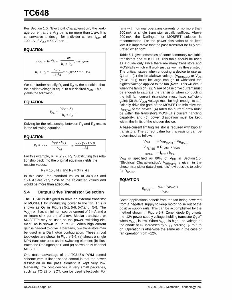
Per Section 1.0, “Electrical Characteristics”, the leak-age current at the VAS pin is no more than 1 µA. It isconservative to design for a divider current, IDIV, of100 µA. If VDD = 5.0V then…
EQUATION
We can further specify R1 and R2 by the condition that the divider voltage is equal to our desired VAS. This yields the following:
EQUATION
Solving for the relationship between R1 and R2 resultsin the following equation:
EQUATION
For this example, R1 = (2.27) R2. Substituting this rela-tionship back into the original equation yields the resistor values:
R2 = 15.3 k, and R1 = 34.7 k
In this case, the standard values of 34.8 k and15.4 k are very close to the calculated values andwould be more than adequate.
5.4 Output Drive Transistor Selection
The TC648 is designed to drive an external transistoror MOSFET for modulating power to the fan. This isshown as Q1 in Figures 5-1, 5-6, 5-7,and 5-8. TheVOUT pin has a minimum source current of 5 mA and aminimum sink current of 1 mA. Bipolar transistors orMOSFETs may be used as the power switching ele-ment, as is shown in Figure 5-6. When high currentgain is needed to drive larger fans, two transistors maybe used in a Darlington configuration. These circuittopologies are shown in Figure 5-6: (a) shows a singleNPN transistor used as the switching element; (b) illus-trates the Darlington pair; and (c) shows an N-channelMOSFET.
One major advantage of the TC648’s PWM controlscheme versus linear speed control is that the powerdissipation in the pass element is kept very low.Generally, low cost devices in very small packages,such as TO-92 or SOT, can be used effectively. For
fans with nominal operating currents of no more than200 mA, a single transistor usually suffices. Above200 mA, the Darlington or MOSFET solution isrecommended. For the power dissipation to be keptlow, it is imperative that the pass transistor be fully sat-urated when "on".
Table 5-1 gives examples of some commonly availabletransistors and MOSFETs. This table should be usedas a guide only since there are many transistors andMOSFETs which will work just as well as those listed.The critical issues when choosing a device to use asQ1 are: (1) the breakdown voltage (V(BR)CEO or VDS(MOSFET)) must be large enough to withstand thehighest voltage applied to the fan (Note: This will occurwhen the fan is off); (2) 5 mA of base drive current mustbe enough to saturate the transistor when conductingthe full fan current (transistor must have sufficientgain); (3) the VOUT voltage must be high enough to suf-ficiently drive the gate of the MOSFET to minimize theRDS(on) of the device; (4) rated fan current draw mustbe within the transistor's/MOSFET's current handlingcapability; and (5) power dissipation must be keptwithin the limits of the chosen device.
A base-current limiting resistor is required with bipolartransistors. The correct value for this resistor can bedetermined as follows:
VOH = VBE(SAT) + VRBASE
VRBASE = RBASE x IBASE
IBASE = IFAN / hFE
VOH is specified as 80% of VDD in Section 1.0,“Electrical Characteristics”; VBE(SAT) is given in thechosen transistor data sheet. It is now possible to solvefor RBASE.
EQUATION
Some applications benefit from the fan being poweredfrom a negative supply to keep motor noise out of thepositive supply rails. This can be accomplished by themethod shown in Figure 5-7. Zener diode D1 offsetsthe -12V power supply voltage, holding transistor Q1 offwhen VOUT is low. When VOUT is high, the voltage atthe anode of D1 increases by VOH, causing Q1 to turnon. Operation is otherwise the same as in the case offan operation from +12V.
R1 + R2IDIV = 1e–4A = , therefore
5.0V
R1 + R2 = = 50,000 = 50 k1e–4A
5.0V
VDD x R2
R1 + R2
VAS =
VDD - VAS
VAS
R1 = R2 x = R2 x (5 - 1.53)
1.53
VOH - VBE(SAT)RBASE =IBASE
DS21448D-page 12 2001-2012 Microchip Technology Inc.

TC648
FIGURE 5-6: Output Drive Transistor Circuit Topologies.
TABLE 5-1: TRANSISTORS AND MOSFETS FOR Q1 (VDD = 5V)
Device PackageMax. VBE(sat)/VGS
(V)Min. HFE
VCEO/VDS(V)
Fan Current (mA)
SuggestedRBASE ()
MMBT2222A SOT-23 1.2 50 40 150 800
MPS2222A TO-92 1.2 50 40 150 800
MPS6602 TO-92 1.2 50 40 500 301
SI2302 SOT-23 2.5 NA 20 500 Note 1
MGSF1N02E SOT-23 2.5 NA 20 500 Note 1
SI4410 SO-8 4.5 NA 30 1000 Note 1
SI2308 SOT-23 4.5 NA 60 500 Note 1
Note 1: A series gate resistor may be used in order to control the MOSFET turn-on and turn-off times.
Q1 Q1
Q2
GND
VDD
RBASEVOUT VOUT
Fan
a) Single Bipolar Transistor
Q1
GND
VDD
VOUT
C) N-Channel MOSFET
GND
VDD
RBASE
Fan
b) Darlington Transistor Pair
Fan
2001-2012 Microchip Technology Inc. DS21448D-page 13

TC648
FIGURE 5-7: Powering the Fan from a -12V Supply.
5.5 Latch-up Considerations
As with any CMOS IC, the potential exists for latch-upif signals are applied to the device which are outsidethe power supply range. This is of particular concernduring power-up if the external circuitry (such as thesensor network, VAS divider or shutdown circuit) arepowered by a supply different from that of the TC648.Care should be taken to ensure that the TC648’s VDDsupply powers up first. If possible, the networksattached to VIN and VAS should connect to the VDD sup-ply at the same physical location as the IC itself. Evenif the IC and any external networks are powered by thesame supply, physical separation of the connectingpoints can result in enough parasitic capacitance and/or inductance in the power supply connections to delayone power supply “routing” versus another.
5.6 Power Supply Routing and Bypassing
Noise present on the VIN and VAS inputs may causeerroneous operation of the OTF output. As a result,these inputs should be bypassed with a 0.01 µF capac-itor mounted as close to the package as possible. Thisis especially true of VIN, which is usually driven from ahigh impedance source (such as a thermistor). Addi-tionally, the VDD input should be bypassed with a 1 µFcapacitor and grounds should be kept as short as pos-sible. To keep fan noise off the TC648 ground pin, indi-vidual ground returns for the TC648 and the low side ofthe fan drive device should be used.
Auto-Shutdown Mode Design Example Step 1. Calculate R1 and R2 based on using an NTC
having a resistance of 10 k at TMIN (25°C)and 4.65 k at TMAX (45°C) (see Figure 5-8).
R1 = 20.5 kR2 = 3.83 k
Step 2. Set auto-shutdown level.
VAS = 1.8V Limit the divider current to 100 µA R5 = 33 kR6 = 18 k
Step 3. Design the output circuit
Maximum fan motor current = 250 mA.Q1 beta is chosen at 50 from which R7 = 800 .
5.7 Minimum Speed Mode Design Example
Given:
Minimum speed = 40%(1.8V)TMIN = 30°C, TMAX = 95°C Thermistor = 100 k at 25°C RTMIN = 79.4 k, RTMAX = 6.5 k
Step 1: Calculate R1:R1 = 7.9 k (Use closest standard value:7.87 k)
Calculate R2:R2 = 4.05 k (Use closest standard value:4.02 k)
Step 2: Verify VMAX: VMAX = 2.64V
GND
+5V
-12V
Q1*
VDD
VOUT
TC648
Fan
R2*2.2 kΩ
R4*
D1
NOTE: *Value depends on the specific application and is shown for example only.
12.0VZener
10 kΩ
DS21448D-page 14 2001-2012 Microchip Technology Inc.

TC648
FIGURE 5-8: Design Example.
5.8 TC648 as a Microcontroller Peripheral
In a system containing a microcontroller or other hostintelligence, the TC648 can be effectively managed asa CPU peripheral. Routine fan control functions can beperformed by the TC648 without processor interven-tion. The microcontroller receives temperature datafrom one or more points throughout the system. Itcalculates a fan operating speed based on an algorithmspecifically designed for the application at hand. Theprocessor controls fan speed using complementaryport bits I/O1 through I/O3.
Resistors R1 through R6 (5% tolerance) form a crude3-bit DAC that translates the 3-bit code from theprocessor's outputs into a 1.6V DC control signal. Amonolithic DAC or digital pot may be used instead ofthe circuit shown in Figure 5-9.
With VAS set at 1.8V, the TC648 enters auto-shutdownwhen the processor's output code is 000[B]. Outputcodes 001[B] to 111[B] operate the fan from roughly40% to 100% of full speed. An open-drain output fromthe processor (I/O0) can be used to reset the TC648following detection of a fault condition. The OTF outputcan be connected to the processor's interrupt input, orto another I/O pin, for polled operation.
NC
NTC10 kΩ
@ 25˚CR120.5 kΩ
R23.83 kΩ
R533 kΩ
R7800Ω
R6
GNDRESET
Shutdown
(Optional) Q1
+12V
+5V
+5V
+5V
VDDVIN
VAS
VOUT
CB1 μF
CF
TC648
OTF
Fan
ThermalFault
CB0.01 μF
CB0.01 μF
CB1 μF
18 4
6
7
5
2
3
18 kΩ
Open-DrainDevice
2001-2012 Microchip Technology Inc. DS21448D-page 15

TC648
FIGURE 5-9: TC648 as a Microcontroller Peripheral.
CMOSMicrocontroller
TC648
VIN
CF
VAS
GND
VDD
VOUT
OTF
NC
+5V
Analog or DigitalTemperature
Data from one ormore Sensors
I/O0
I/O1
I/O2
I/O3
INTGND
(Optional)
(MSB)
R1110 kΩ
R2240 kΩ
R3360 kΩ
(LSB)
R51.5 kΩ
+5V
R61 kΩ
R418 kΩ
R733 kΩ
+5V R818 kΩ
CB
.01 μF
+
1 μF
CB
.01 μFCMOSOutputs
Open-Drain Outputs
Fan
+12V
+5V
CB
1 μF+
R9800Ω
+5V
R1010 kΩ
2N2222A
1
2
3
4 5
6
7
8
(RESET)
DS21448D-page 16 2001-2012 Microchip Technology Inc.
TC648
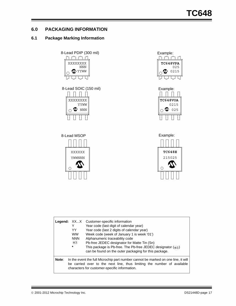
6.0 PACKAGING INFORMATION
6.1 Package Marking Information
XXXXXXXXNNNYYWW
8-Lead PDIP (300 mil) Example:
8-Lead SOIC (150 mil) Example:
XXXXXXXXYYWW
NNN
TC648VPA025
0215
TC648VOA0215
025
8-Lead MSOP Example:
XXXXXX
YWWNNN
TC648E
215025
Legend: XX...X Customer-specific informationY Year code (last digit of calendar year)YY Year code (last 2 digits of calendar year)WW Week code (week of January 1 is week ‘01’)NNN Alphanumeric traceability code Pb-free JEDEC designator for Matte Tin (Sn)* This package is Pb-free. The Pb-free JEDEC designator ( )
can be found on the outer packaging for this package.
Note: In the event the full Microchip part number cannot be marked on one line, it willbe carried over to the next line, thus limiting the number of availablecharacters for customer-specific information.
3e
3e
2001-2012 Microchip Technology Inc. DS21448D-page 17

TC648
8-Lead Plastic Dual In-line (P) – 300 mil (PDIP)
B1
B
A1
A
L
A2
p
E
eB
c
E1
n
D
1
2
Units INCHES* MILLIMETERS
Dimension Limits MIN NOM MAX MIN NOM MAX
Number of Pins n 8 8
Pitch p .100 2.54
Top to Seating Plane A .140 .155 .170 3.56 3.94 4.32
Molded Package Thickness A2 .115 .130 .145 2.92 3.30 3.68
Base to Seating Plane A1 .015 0.38
Shoulder to Shoulder Width E .300 .313 .325 7.62 7.94 8.26
Molded Package Width E1 .240 .250 .260 6.10 6.35 6.60
Overall Length D .360 .373 .385 9.14 9.46 9.78
Tip to Seating Plane L .125 .130 .135 3.18 3.30 3.43
Lead Thickness c .008 .012 .015 0.20 0.29 0.38
Upper Lead Width B1 .045 .058 .070 1.14 1.46 1.78
Lower Lead Width B .014 .018 .022 0.36 0.46 0.56
Overall Row Spacing § eB .310 .370 .430 7.87 9.40 10.92
Mold Draft Angle Top 5 10 15 5 10 15
Mold Draft Angle Bottom 5 10 15 5 10 15
* Controlling Parameter
Notes:Dimensions D and E1 do not include mold flash or protrusions. Mold flash or protrusions shall not exceed
JEDEC Equivalent: MS-001Drawing No. C04-018
.010” (0.254mm) per side.
§ Significant Characteristic
Note: For the most current package drawings, please see the Microchip Packaging Specification locatedat http://www.microchip.com/packaging
DS21448D-page 18 2001-2012 Microchip Technology Inc.

TC648
8-Lead Plastic Small Outline (SN) – Narrow, 150 mil (SOIC)
Foot Angle f 0 4 8 0 4 8
1512015120Mold Draft Angle Bottom
1512015120Mold Draft Angle Top
0.510.420.33.020.017.013BLead Width
0.250.230.20.010.009.008cLead Thickness
0.760.620.48.030.025.019LFoot Length
0.510.380.25.020.015.010hChamfer Distance
5.004.904.80.197.193.189DOverall Length
3.993.913.71.157.154.146E1Molded Package Width
6.206.025.79.244.237.228EOverall Width
0.250.180.10.010.007.004A1Standoff §
1.551.421.32.061.056.052A2Molded Package Thickness
1.751.551.35.069.061.053AOverall Height
1.27.050pPitch
88nNumber of Pins
MAXNOMMINMAXNOMMINDimension Limits
MILLIMETERSINCHES*Units
2
1
D
n
p
B
E
E1
h
L
c
45×
f
A2
A
A1
* Controlling Parameter
Notes:Dimensions D and E1 do not include mold flash or protrusions. Mold flash or protrusions shall not exceed .010” (0.254mm) per side.JEDEC Equivalent: MS-012Drawing No. C04-057
§ Significant Characteristic
Note: For the most current package drawings, please see the Microchip Packaging Specification locatedat http://www.microchip.com/packaging
2001-2012 Microchip Technology Inc. DS21448D-page 19

TC648
8-Lead Plastic Micro Small Outline Package (MS) (MSOP)
p
A
A1
A2
D
L
c
Dimensions D and E1 do not include mold flash or protrusions. Mold flash or protrusions shall not
.037.035FFootprint (Reference)
exceed. 010" (0.254mm) per side.
Notes:
Drawing No. C04-111
*Controlling Parameter
Mold Draft Angle Top
Mold Draft Angle Bottom
Foot Angle
Lead Width
Lead Thickness
c
B
7
7
.004
.010
0
.006
.012
(F)
Dimension Limits
Overall Height
Molded Package Thickness
Molded Package Width
Overall Length
Foot Length
Standoff §
Overall Width
Number of Pins
Pitch
A
L
E1
D
A1
E
A2
.016
.114
.114
.022
.118
.118
.002
.030
.193
.034
MIN
p
n
Units
.026
NOM
8
INCHES
1.000.950.90.039
0.15
0.30
.008
.016
6
0.10
0.25
0
7
7
0.20
0.40
6
MILLIMETERS*
0.65
0.86
3.00
3.00
0.55
4.90
.044
.122
.028
.122
.038
.006
0.40
2.90
2.90
0.05
0.76
MINMAX NOM
1.18
0.70
3.10
3.10
0.15
0.97
MAX
8
E1
E
B
n 1
2
§ Significant Characteristic
.184 .200 4.67 .5.08
Note: For the most current package drawings, please see the Microchip Packaging Specification locatedat http://www.microchip.com/packaging
DS21448D-page 20 2001-2012 Microchip Technology Inc.

TC648
6.2 Taping Form
Component Taping Orientation for 8-Pin SOIC (Narrow) Devices
Package Carrier Width (W) Pitch (P) Part Per Full Reel Reel Size
8-Pin SOIC (N) 12 mm 8 mm 2500 13 in
Carrier Tape, Number of Components Per Reel and Reel Size
Standard Reel Component Orientationfor 713 Suffix Device
PIN 1
User Direction of Feed
P
W
PIN 1
Component Taping Orientation for 8-Pin MSOP Devices
User Direction of Feed
Standard Reel Component Orientationfor 713 Suffix Device
W
P
Package Carrier Width (W) Pitch (P) Part Per Full Reel Reel Size
8-Pin MSOP 12 mm 8 mm 2500 13 in
Carrier Tape, Number of Components Per Reel and Reel Size
2001-2012 Microchip Technology Inc. DS21448D-page 21

TC648
7.0 REVISION HISTORY
Revision D (December 2012)
Added a note to each package outline drawing.
DS21448D-page 22 2001-2012 Microchip Technology Inc.

THE MICROCHIP WEB SITE
Microchip provides online support via our WWW site atwww.microchip.com. This web site is used as a meansto make files and information easily available tocustomers. Accessible by using your favorite Internetbrowser, the web site contains the followinginformation:
• Product Support – Data sheets and errata, application notes and sample programs, design resources, user’s guides and hardware support documents, latest software releases and archived software
• General Technical Support – Frequently Asked Questions (FAQ), technical support requests, online discussion groups, Microchip consultant program member listing
• Business of Microchip – Product selector and ordering guides, latest Microchip press releases, listing of seminars and events, listings of Microchip sales offices, distributors and factory representatives
CUSTOMER CHANGE NOTIFICATION SERVICE
Microchip’s customer notification service helps keepcustomers current on Microchip products. Subscriberswill receive e-mail notification whenever there arechanges, updates, revisions or errata related to aspecified product family or development tool of interest.
To register, access the Microchip web site atwww.microchip.com. Under “Support”, click on“Customer Change Notification” and follow theregistration instructions.
CUSTOMER SUPPORT
Users of Microchip products can receive assistancethrough several channels:
• Distributor or Representative
• Local Sales Office
• Field Application Engineer (FAE)
• Technical Support
Customers should contact their distributor,representative or field application engineer (FAE) forsupport. Local sales offices are also available to helpcustomers. A listing of sales offices and locations isincluded in the back of this document.
Technical support is available through the web siteat: http://microchip.com/support
2001-2012 Microchip Technology Inc. DS21448D-page 23

READER RESPONSE
It is our intention to provide you with the best documentation possible to ensure successful use of your Microchipproduct. If you wish to provide your comments on organization, clarity, subject matter, and ways in which ourdocumentation can better serve you, please FAX your comments to the Technical Publications Manager at(480) 792-4150.
Please list the following information, and use this outline to provide us with your comments about this document.
TO: Technical Publications Manager
RE: Reader ResponseTotal Pages Sent ________
From: Name
Company
Address
City / State / ZIP / Country
Telephone: (_______) _________ - _________
Application (optional):
Would you like a reply? Y N
Device: Literature Number:
Questions:
FAX: (______) _________ - _________
DS21448D
1. What are the best features of this document?
2. How does this document meet your hardware and software development needs?
3. Do you find the organization of this document easy to follow? If not, why?
4. What additions to the document do you think would enhance the structure and subject?
5. What deletions from the document could be made without affecting the overall usefulness?
6. Is there any incorrect or misleading information (what and where)?
7. How would you improve this document?
DS21448D-page 24 2001-2012 Microchip Technology Inc.

TC648
PRODUCT IDENTIFICATION SYSTEM
To order or obtain information, e.g., on pricing or delivery, refer to the factory or the listed sales office.
Sales and Support
Data SheetsProducts supported by a preliminary Data Sheet may have an errata sheet describing minor operational differences and recom-mended workarounds. To determine if an errata sheet exists for a particular device, please contact one of the following:
1. Your local Microchip sales office2. The Microchip Worldwide Site (www.microchip.com)
Please specify which device, revision of silicon and Data Sheet (include Literature #) you are using.
New Customer Notification SystemRegister on our web site (www.microchip.com/cn) to receive the most current information on our products.
PART NO. X /XX
PackageTemperatureRange
Device
Device: TC648: PWM Fan Speed Controller w/Auto Shutdown and Overtemperature Alert
Temperature Range: V = 0C to +85CE = -40C to +85C
Package: PA = Plastic DIP (300 mil Body), 8-leadOA = Plastic SOIC, (150 mil Body), 8-leadUA = Plastic Micro Small Outline (MSOP), 8-lead
* PDIP package is only offered in the V temp range
Examples:
a) TC648VOA: PWM Fan Speed Controllerw/Auto Shutdown and Over-Temperature Alert,SOIC package.
b) TC648VUA: PWM Fan Speed Controllerw/Auto Shutdown and Over-Temperature Alert,MSOP package.
c) TC648VPA: PWM Fan Speed Controllerw/Auto Shutdown and Over-Temperature Alert,PDIP package.
d) TC648EOA713: PWM Fan Speed Controllerw/Auto Shutdown and Over-Temperature Alert,SOIC package, Tape and Reel.
2001-2012 Microchip Technology Inc. DS21448D-page25

TC648
NOTES:
DS21448D-page 26 2001-2012 Microchip Technology Inc.
Note the following details of the code protection feature on Microchip devices:
• Microchip products meet the specification contained in their particular Microchip Data Sheet.
• Microchip believes that its family of products is one of the most secure families of its kind on the market today, when used in the intended manner and under normal conditions.
• There are dishonest and possibly illegal methods used to breach the code protection feature. All of these methods, to our knowledge, require using the Microchip products in a manner outside the operating specifications contained in Microchip’s Data Sheets. Most likely, the person doing so is engaged in theft of intellectual property.
• Microchip is willing to work with the customer who is concerned about the integrity of their code.
• Neither Microchip nor any other semiconductor manufacturer can guarantee the security of their code. Code protection does not mean that we are guaranteeing the product as “unbreakable.”
Code protection is constantly evolving. We at Microchip are committed to continuously improving the code protection features of ourproducts. Attempts to break Microchip’s code protection feature may be a violation of the Digital Millennium Copyright Act. If such actsallow unauthorized access to your software or other copyrighted work, you may have a right to sue for relief under that Act.
Information contained in this publication regarding deviceapplications and the like is provided only for your convenienceand may be superseded by updates. It is your responsibility toensure that your application meets with your specifications.MICROCHIP MAKES NO REPRESENTATIONS ORWARRANTIES OF ANY KIND WHETHER EXPRESS ORIMPLIED, WRITTEN OR ORAL, STATUTORY OROTHERWISE, RELATED TO THE INFORMATION,INCLUDING BUT NOT LIMITED TO ITS CONDITION,QUALITY, PERFORMANCE, MERCHANTABILITY ORFITNESS FOR PURPOSE. Microchip disclaims all liabilityarising from this information and its use. Use of Microchipdevices in life support and/or safety applications is entirely atthe buyer’s risk, and the buyer agrees to defend, indemnify andhold harmless Microchip from any and all damages, claims,suits, or expenses resulting from such use. No licenses areconveyed, implicitly or otherwise, under any Microchipintellectual property rights.
2001-2012 Microchip Technology Inc.
QUALITY MANAGEMENT SYSTEM CERTIFIED BY DNV
== ISO/TS 16949 ==
Trademarks
The Microchip name and logo, the Microchip logo, dsPIC, FlashFlex, KEELOQ, KEELOQ logo, MPLAB, PIC, PICmicro, PICSTART, PIC32 logo, rfPIC, SST, SST Logo, SuperFlash and UNI/O are registered trademarks of Microchip Technology Incorporated in the U.S.A. and other countries.
FilterLab, Hampshire, HI-TECH C, Linear Active Thermistor, MTP, SEEVAL and The Embedded Control Solutions Company are registered trademarks of Microchip Technology Incorporated in the U.S.A.
Silicon Storage Technology is a registered trademark of Microchip Technology Inc. in other countries.
Analog-for-the-Digital Age, Application Maestro, BodyCom, chipKIT, chipKIT logo, CodeGuard, dsPICDEM, dsPICDEM.net, dsPICworks, dsSPEAK, ECAN, ECONOMONITOR, FanSense, HI-TIDE, In-Circuit Serial Programming, ICSP, Mindi, MiWi, MPASM, MPF, MPLAB Certified logo, MPLIB, MPLINK, mTouch, Omniscient Code Generation, PICC, PICC-18, PICDEM, PICDEM.net, PICkit, PICtail, REAL ICE, rfLAB, Select Mode, SQI, Serial Quad I/O, Total Endurance, TSHARC, UniWinDriver, WiperLock, ZENA and Z-Scale are trademarks of Microchip Technology Incorporated in the U.S.A. and other countries.
SQTP is a service mark of Microchip Technology Incorporated in the U.S.A.
GestIC and ULPP are registered trademarks of Microchip Technology Germany II GmbH & Co. & KG, a subsidiary of Microchip Technology Inc., in other countries.
All other trademarks mentioned herein are property of their respective companies.
© 2001-2012, Microchip Technology Incorporated, Printed in the U.S.A., All Rights Reserved.
Printed on recycled paper.
ISBN: 9781620768297
Microchip received ISO/TS-16949:2009 certification for its worldwide
DS21448D-page 27
headquarters, design and wafer fabrication facilities in Chandler and Tempe, Arizona; Gresham, Oregon and design centers in California and India. The Company’s quality system processes and procedures are for its PIC® MCUs and dsPIC® DSCs, KEELOQ® code hopping devices, Serial EEPROMs, microperipherals, nonvolatile memory and analog products. In addition, Microchip’s quality system for the design and manufacture of development systems is ISO 9001:2000 certified.

DS21448D-page 28 2001-2012 Microchip Technology Inc.
AMERICASCorporate Office2355 West Chandler Blvd.Chandler, AZ 85224-6199Tel: 480-792-7200 Fax: 480-792-7277Technical Support: http://www.microchip.com/supportWeb Address: www.microchip.com
AtlantaDuluth, GA Tel: 678-957-9614 Fax: 678-957-1455
BostonWestborough, MA Tel: 774-760-0087 Fax: 774-760-0088
ChicagoItasca, IL Tel: 630-285-0071 Fax: 630-285-0075
ClevelandIndependence, OH Tel: 216-447-0464 Fax: 216-447-0643
DallasAddison, TX Tel: 972-818-7423 Fax: 972-818-2924
DetroitFarmington Hills, MI Tel: 248-538-2250Fax: 248-538-2260
IndianapolisNoblesville, IN Tel: 317-773-8323Fax: 317-773-5453
Los AngelesMission Viejo, CA Tel: 949-462-9523 Fax: 949-462-9608
Santa ClaraSanta Clara, CA Tel: 408-961-6444Fax: 408-961-6445
TorontoMississauga, Ontario, CanadaTel: 905-673-0699 Fax: 905-673-6509
ASIA/PACIFICAsia Pacific OfficeSuites 3707-14, 37th FloorTower 6, The GatewayHarbour City, KowloonHong KongTel: 852-2401-1200Fax: 852-2401-3431
Australia - SydneyTel: 61-2-9868-6733Fax: 61-2-9868-6755
China - BeijingTel: 86-10-8569-7000 Fax: 86-10-8528-2104
China - ChengduTel: 86-28-8665-5511Fax: 86-28-8665-7889
China - ChongqingTel: 86-23-8980-9588Fax: 86-23-8980-9500
China - HangzhouTel: 86-571-2819-3187 Fax: 86-571-2819-3189
China - Hong Kong SARTel: 852-2943-5100 Fax: 852-2401-3431
China - NanjingTel: 86-25-8473-2460Fax: 86-25-8473-2470
China - QingdaoTel: 86-532-8502-7355Fax: 86-532-8502-7205
China - ShanghaiTel: 86-21-5407-5533 Fax: 86-21-5407-5066
China - ShenyangTel: 86-24-2334-2829Fax: 86-24-2334-2393
China - ShenzhenTel: 86-755-8864-2200 Fax: 86-755-8203-1760
China - WuhanTel: 86-27-5980-5300Fax: 86-27-5980-5118
China - XianTel: 86-29-8833-7252Fax: 86-29-8833-7256
China - XiamenTel: 86-592-2388138 Fax: 86-592-2388130
China - ZhuhaiTel: 86-756-3210040 Fax: 86-756-3210049
ASIA/PACIFICIndia - BangaloreTel: 91-80-3090-4444 Fax: 91-80-3090-4123
India - New DelhiTel: 91-11-4160-8631Fax: 91-11-4160-8632
India - PuneTel: 91-20-2566-1512Fax: 91-20-2566-1513
Japan - OsakaTel: 81-6-6152-7160 Fax: 81-6-6152-9310
Japan - TokyoTel: 81-3-6880- 3770 Fax: 81-3-6880-3771
Korea - DaeguTel: 82-53-744-4301Fax: 82-53-744-4302
Korea - SeoulTel: 82-2-554-7200Fax: 82-2-558-5932 or 82-2-558-5934
Malaysia - Kuala LumpurTel: 60-3-6201-9857Fax: 60-3-6201-9859
Malaysia - PenangTel: 60-4-227-8870Fax: 60-4-227-4068
Philippines - ManilaTel: 63-2-634-9065Fax: 63-2-634-9069
SingaporeTel: 65-6334-8870Fax: 65-6334-8850
Taiwan - Hsin ChuTel: 886-3-5778-366Fax: 886-3-5770-955
Taiwan - KaohsiungTel: 886-7-213-7828Fax: 886-7-330-9305
Taiwan - TaipeiTel: 886-2-2508-8600 Fax: 886-2-2508-0102
Thailand - BangkokTel: 66-2-694-1351Fax: 66-2-694-1350
EUROPEAustria - WelsTel: 43-7242-2244-39Fax: 43-7242-2244-393Denmark - CopenhagenTel: 45-4450-2828 Fax: 45-4485-2829
France - ParisTel: 33-1-69-53-63-20 Fax: 33-1-69-30-90-79
Germany - MunichTel: 49-89-627-144-0 Fax: 49-89-627-144-44
Italy - Milan Tel: 39-0331-742611 Fax: 39-0331-466781
Netherlands - DrunenTel: 31-416-690399 Fax: 31-416-690340
Spain - MadridTel: 34-91-708-08-90Fax: 34-91-708-08-91
UK - WokinghamTel: 44-118-921-5869Fax: 44-118-921-5820
Worldwide Sales and Service
11/29/12