Embed Size (px)
Citation preview

TC6320N-Channel and P-Channel Enhancement-Mode MOSFET Pair
Features
• Integrated Gate-to-source Resistor
• Integrated Gate-to-source Zener Diode
• Low Threshold
• Low On-resistance
• Low Input Capacitance
• Fast Switching Speeds
• Free from Secondary Breakdown
• Low Input and Output Leakage
• Independent Electrically Isolated N-channel and P-channel
Applications
• High-voltage Pulsers
• Amplifiers
• Buffers
• Piezoelectric Transducer Drivers
• General Purpose Line Drivers
• Logic-level Interfaces
General Description
The TC6320 consists of high-voltage, low-threshold N-channel and P-channel MOSFETs in 8-lead SOIC and DFN packages. Both MOSFETs have integrated gate-to-source resistors and gate-to-source Zener diode clamps which are desired for high-voltage pulser applications. It is a complimentary, high-speed, high-voltage, gate-clamped N-channel and P-channel MOSFET pair, which utilizes an advanced vertical DMOS structure and a well-proven silicon gate manufacturing process. This combination produces a device with the power handling capabilities of bipolar transistors and with the high input impedance and positive temperature coefficient inherent in MOS devices. Characteristic of all MOS structures, this device is free from thermal runaway and thermally induced secondary breakdown.
Microchip’s vertical DMOS FETs are ideally suited to a wide range of switching and amplifying applications where very low threshold voltage, high breakdown voltage, high input impedance, low input capacitance and fast switching speeds are desired.
Package Type
8-lead SOIC(Top view)
See Table 2-1 and Table 2-2 for pin information.
8
7
6
5
1
2
3
4
SN
GN
SP
GP
DN
DN
DP
DP
5-lead DFN(Top view)
8
7
6
5
1
2
3
4
SN
GN
GP
SP
DN
DN
DP
DP
DN
DP
s
2017 Microchip Technology Inc. DS20005697A-page 1

TC6320
Functional Block Diagram
N-ChannelP-Channel
DN
DN
DP
DP
SN
GN
GP
SP
DS20005697A-page 2 2017 Microchip Technology Inc.

TC6320
Typical Application Circuit
VSS VL
VDD VH
INA
INB
OE
-100V
+100V
TC6320
10nF
10nF
MD12xx, MD17xx, or MD18xx
2017 Microchip Technology Inc. DS20005697A-page 3

TC6320
1.0 ELECTRICAL CHARACTERISTICS
Absolute Maximum Ratings†
Drain-to-source Voltage ........................................................................................................................................ BVDSSDrain-to-gate Voltage ........................................................................................................................................... BVDGSOperating Ambient Temperature, TA ................................................................................................... –55°C to +150°CStorage Temperature, TS ..................................................................................................................... –55°C to +150°C
† Notice: Stresses above those listed under “Absolute Maximum Ratings” may cause permanent damage to the device. This is a stress rating only, and functional operation of the device at those or any other conditions above those indicated in the operational sections of this specification is not intended. Exposure to maximum rating conditions for extended periods may affect device reliability.
N-CHANNEL ELECTRICAL CHARACTERISTICS Electrical Specifications: TA = TJ = 25°C unless otherwise specified.
Parameter Sym. Min. Typ. Max. Unit Conditions
DC PARAMETER (Note 1 unless otherwise specified)
Drain-to-source Breakdown Voltage BVDSS 200 — — V VGS = 0V, ID = 2 mA
Gate Threshold Voltage VGS(th) 1 — 2 V VGS = VDS, ID = 1 mA
Change in VGS(th) with Temperature ∆VGS(th) — — –4.5 mV/°C VGS = VDS, ID = 1 mA (Note 2)
Gate-to-source Shunt Resistor RGS 10 — 50 kΩ IGS = 100 µA
Gate-to-Source Zener Voltage VZGS 13.2 — 25 V IGS = 2 mA
Zero-gate Voltage Drain Current IDSS
— — 10 µAVDS = Maximum rating, VGS = 0V
— — 1 mAVDS = 0.8 Maximum rating, VGS = 0V, TA = 125°C (Note 2)
On-state Drain Current ID(ON)1 — —
AVGS = 4.5V, VDS = 25V
2 — — VGS = 10V, VDS = 25V
Static Drain-to-source On-state Resistance
RDS(ON)— — 8
ΩVGS = 4.5V, ID = 150 mA
— — 7 VGS = 10V, ID = 1A
Change in RDS(ON) with Temperature ∆RDS(ON) — — 1 %/°C VGS = 4.5V, ID = 150 mA (Note 2)
AC PARAMETER (Note 2)
Forward Transconductance GFS 400 — — mmho VDS = 25V, ID = 500 mA
Input Capacitance CISS — — 110 pF VGS = 0V, VDS = 25V,f = 1 MHz
Common Source Output Capacitance COSS — — 60 pF
Reverse Transfer Capacitance CRSS — — 23 pF
Turn-on Delay Time td(ON) — — 10 nsVDD = 25V, ID = 1A, RGEN = 25Ω
Rise Time tr — — 15 ns
Turn-off Delay Time td(OFF) — — 20 ns
Fall Time tf — — 15 ns
DIODE PARAMETER
Diode Forward Voltage Drop VSD — — 1.8 V VGS = 0V, ISD = 500 mA (Note 1)
Reverse Recovery Time trr — 300 — ns VGS = 0V, ISD = 500 mA (Note 2)
Note 1: All DC parameters are 100% tested at 25°C unless otherwise stated. Pulse test: 300 µs pulse, 2% duty cycle.
2: Specification is obtained by characterization and is not 100% tested.
DS20005697A-page 4 2017 Microchip Technology Inc.

TC6320
P-CHANNEL ELECTRICAL CHARACTERISTICS Electrical Specifications: TA = TJ = 25°C unless otherwise specified.
Parameter Sym. Min. Typ. Max. Unit Conditions
DC PARAMETER (Note 1 unless otherwise specified)
Drain-to-source Breakdown Voltage BVDSS –200 — — V VGS = 0V, ID = –2 mA
Gate Threshold Voltage VGS(th) –1 — –2.4 V VGS = VDS, ID = –1 mA
Change in VGS(th) with Temperature ∆VGS(th) — — 4.5 mV/°C VGS = VDS, ID = –1 mA (Note 2)
Gate-to-source Shunt Resistor RGS 10 — 50 kΩ IGS = 100 µA
Gate-to-Source Zener Voltage VZGS 13.2 — 25 V IGS = –2 mA
Zero-gate Voltage Drain Current IDSS
— — –10 µAVDS = Maximum rating, VGS = 0V
— — –1 mAVDS = 0.8 Maximum rating,VGS = 0V, TA = 125°C (Note 2)
On-state Drain Current ID(ON)–1 — —
AVGS = –4.5V, VDS = –25V
–2 — — VGS = –10V, VDS = –25V
Static Drain-to-source On-state Resistance
RDS(ON)— — 10
ΩVGS = –4.5V, ID = –150 mA
— — 8 VGS = –10V, ID = –1A
Change in RDS(ON) with Temperature ∆RDS(ON) — — 1 %/°C VGS = –10V, ID = –200 mA (Note 2)
AC PARAMETER (Note 2)
Forward Transconductance GFS 400 — — mmho VDS = –25V, ID = –500 mA
Input Capacitance CISS — — 200 pFVGS = 0V, VDS = –25V,f = 1 MHz
Common Source Output Capacitance
COSS — — 55 pF
Reverse Transfer Capacitance CRSS — — 30 pF
Turn-on Delay Time td(ON) — — 10 nsVDD = –25V, ID = –1A, RGEN = 25Ω
Rise Time tr — — 15 ns
Turn-off Delay Time td(OFF) — — 20 ns
Fall Time tf — — 15 ns
DIODE PARAMETER
Diode Forward Voltage Drop VSD — — –1.8 V VGS = 0V, ISD = –500 mA (Note 1)
Reverse Recovery Time trr — 300 — ns VGS = 0V, ISD = –500 mA (Note 2)
Note 1: All DC parameters are 100% tested at 25°C unless otherwise stated. Pulse test: 300 µs pulse, 2% duty cycle.
2: Specification is obtained by characterization and is not 100% tested.
TEMPERATURE SPECIFICATIONSElectrical Characteristics: Unless otherwise specified, for all specifications TA =TJ = +25°C.
Parameter Sym. Min. Typ. Max. Unit Conditions
TEMPERATURE RANGE
Operating Ambient Temperature TA –55°C — +150 °C
Storage Temperature TS –55°C — +150 °C
PACKAGE THERMAL RESISTANCE
8-lead DFN JA — 44 — °C/W Note 1
8-lead SOIC JA — 101 — °C/W Note 1Note 1: 1 oz., four-layer, 3” x 4” PCB
2017 Microchip Technology Inc. DS20005697A-page 5
TC6320
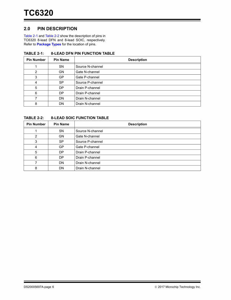
2.0 PIN DESCRIPTION
Table 2-1 and Table 2-2 show the description of pins in TC6320 8-lead DFN and 8-lead SOIC, respectively. Refer to Package Types for the location of pins.
TABLE 2-1: 8-LEAD DFN PIN FUNCTION TABLE
Pin Number Pin Name Description
1 SN Source N-channel
2 GN Gate N-channel
3 GP Gate P-channel
4 SP Source P-channel
5 DP Drain P-channel
6 DP Drain P-channel
7 DN Drain N-channel
8 DN Drain N-channel
TABLE 2-2: 8-LEAD SOIC FUNCTION TABLE
Pin Number Pin Name Description
1 SN Source N-channel
2 GN Gate N-channel
3 SP Source P-channel
4 GP Gate P-channel
5 DP Drain P-channel
6 DP Drain P-channel
7 DN Drain N-channel
8 DN Drain N-channel
DS20005697A-page 6 2017 Microchip Technology Inc.

TC6320
3.0 FUNCTIONAL DESCRIPTION
Figure 3-1 and Figure 3-2 illustrate the switching waveforms and test circuits for TC6320.
10V
0V
0V
VDD
Input
Output
10%
90%
90%
10%
90%
10%
RGEN
Input
Pulse Generator
VDD
RL
D.U.T
OUTPUT
tr tftd(ON)
t(ON)
td(OFF)
t(OFF)
FIGURE 3-1: N-Channel Switching Waveforms and Test Circuit.
RGEN
Input
Pulse Generator
VDD
RL
D.U.T
OUTPUT
0V
-10V
0V
VDD
Input
Output
tr tftd(ON)
t(ON)
90%
10%
90%
10%
10%
90%
td(OFF)
t(OFF)
FIGURE 3-2: P-Channel Switching Waveforms and Test Circuit.
PRODUCT SUMMARY
BVDSS/BVDGS(V)
RDS(ON)(Maximum)
(Ω)
N-Channel P-Channel N-Channel P-Channel
200 –200 7 8
2017 Microchip Technology Inc. DS20005697A-page 7

TC6320
4.0 PACKAGING INFORMATION
4.1 Package Marking Information
Legend: XX...X Product Code or Customer-specific informationY Year code (last digit of calendar year)YY Year code (last 2 digits of calendar year)WW Week code (week of January 1 is week ‘01’)NNN Alphanumeric traceability code Pb-free JEDEC® designator for Matte Tin (Sn)* This package is Pb-free. The Pb-free JEDEC designator ( )
can be found on the outer packaging for this package.
Note: In the event the full Microchip part number cannot be marked on one line, it will be carried over to the next line, thus limiting the number of available characters for product code or customer-specific information. Package may or not include the corporate logo.
3e
3e
8-lead DFN Example
NNN
XXXXXXXXXXXXXX
YYWWe3
222
K6TC6320
1715e3
8-lead SOIC Example
NNN
XXXXXXXYYWW
555
TC6320TG1727e3e3
DS20005697A-page 8 2017 Microchip Technology Inc.
TC6320
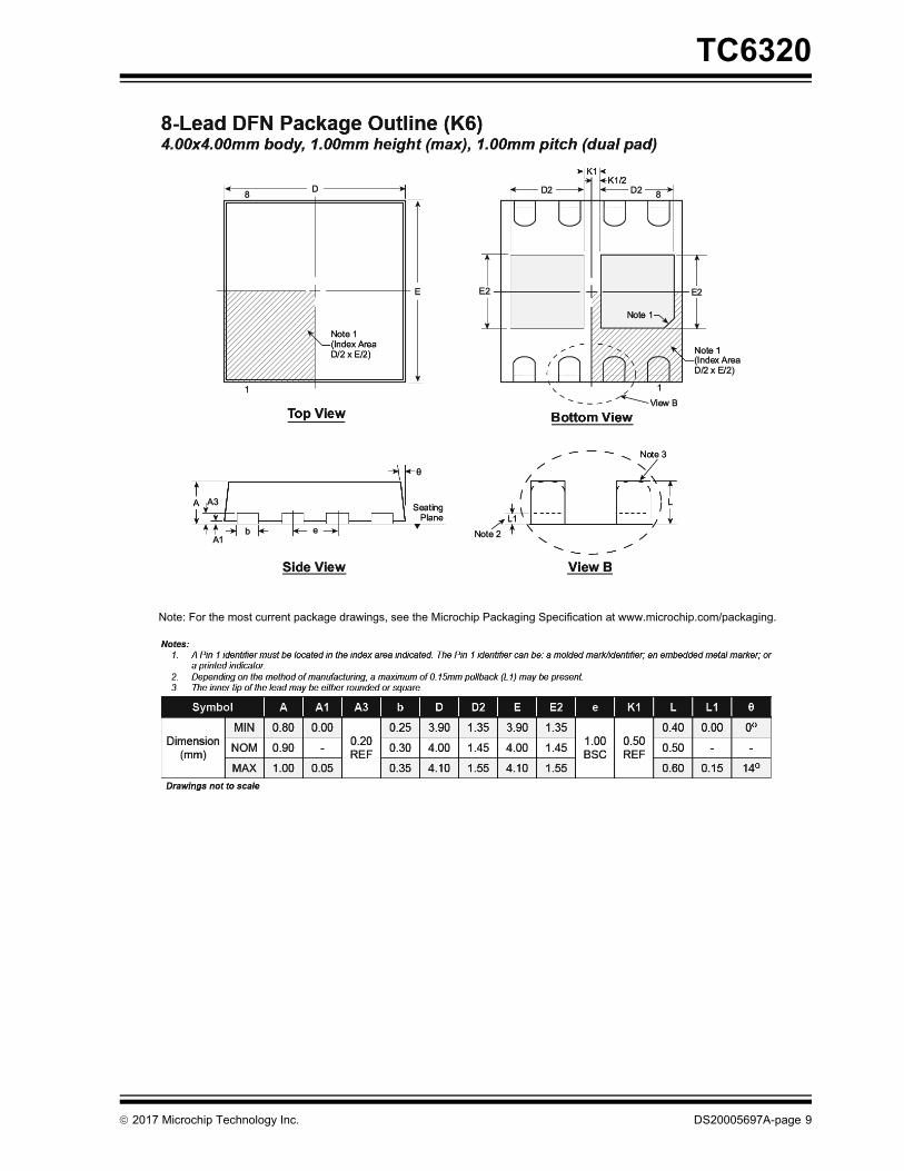
Note: For the most current package drawings, see the Microchip Packaging Specification at www.microchip.com/packaging.
2017 Microchip Technology Inc. DS20005697A-page 9

TC6320
Note: For the most current package drawings, see the Microchip Packaging Specification at www.microchip.com/packaging.
DS20005697A-page 10 2017 Microchip Technology Inc.

2017 Microchip Technology Inc. DS20005697A-page 11
TC6320
APPENDIX A: REVISION HISTORY
Revision A (October 2017)
• Converted Supertex Doc# DSFP-TC6320 to Microchip DS20005697A
• Changed the package marking format
• Changed the quantity of the 8-lead DFN K6 package from 3000/Reel to 3300/Reel
• Changed the quantity of the 8-lead SOIC TG package from 2000/Reel to 3300/Reel
• Made minor text changes throughout the docu-ment

TC6320
DS20005697A-page 12 2017 Microchip Technology Inc.
PRODUCT IDENTIFICATION SYSTEM
To order or obtain information, e.g., on pricing or delivery, contact your local Microchip representative or sales office.
Examples:
a) TC6320K6-G: N-Channel and P-Channel
Enhancement-Mode MOSFET Pair, 8‐lead (4x4) VDFN, 3300/Reel
b) TC6320TG-G: N-Channel and P-Channel Enhancement-Mode MOSFET Pair, 8-lead SOIC, 3300/Reel
PART NO.
Device
Device: TC6320 = N-Channel and P-Channel Enhancement-Mode MOSFET Pair
Packages: K6 = 8-lead (4x4) VDFN
TG = 8-lead SOIC
Environmental: G = Lead (Pb)-free/RoHS-compliant Package
Media Type: (blank) = 3300/Reel for a K6 Package
= 3300/Reel for a TG Package
XX
Package
- X - X
Environmental Media Type Options

Note the following details of the code protection feature on Microchip devices:
• Microchip products meet the specification contained in their particular Microchip Data Sheet.
• Microchip believes that its family of products is one of the most secure families of its kind on the market today, when used in the intended manner and under normal conditions.
• There are dishonest and possibly illegal methods used to breach the code protection feature. All of these methods, to our knowledge, require using the Microchip products in a manner outside the operating specifications contained in Microchip’s Data Sheets. Most likely, the person doing so is engaged in theft of intellectual property.
• Microchip is willing to work with the customer who is concerned about the integrity of their code.
• Neither Microchip nor any other semiconductor manufacturer can guarantee the security of their code. Code protection does not mean that we are guaranteeing the product as “unbreakable.”
Code protection is constantly evolving. We at Microchip are committed to continuously improving the code protection features of our products. Attempts to break Microchip’s code protection feature may be a violation of the Digital Millennium Copyright Act. If such acts allow unauthorized access to your software or other copyrighted work, you may have a right to sue for relief under that Act.
Information contained in this publication regarding device applications and the like is provided only for your convenience and may be superseded by updates. It is your responsibility to ensure that your application meets with your specifications. MICROCHIP MAKES NO REPRESENTATIONS OR WARRANTIES OF ANY KIND WHETHER EXPRESS OR IMPLIED, WRITTEN OR ORAL, STATUTORY OR OTHERWISE, RELATED TO THE INFORMATION, INCLUDING BUT NOT LIMITED TO ITS CONDITION, QUALITY, PERFORMANCE, MERCHANTABILITY OR FITNESS FOR PURPOSE. Microchip disclaims all liability arising from this information and its use. Use of Microchip devices in life support and/or safety applications is entirely at the buyer’s risk, and the buyer agrees to defend, indemnify and hold harmless Microchip from any and all damages, claims, suits, or expenses resulting from such use. No licenses are conveyed, implicitly or otherwise, under any Microchip intellectual property rights unless otherwise stated.
2017 Microchip Technology Inc.
Microchip received ISO/TS-16949:2009 certification for its worldwide headquarters, design and wafer fabrication facilities in Chandler and Tempe, Arizona; Gresham, Oregon and design centers in California and India. The Company’s quality system processes and procedures are for its PIC® MCUs and dsPIC® DSCs, KEELOQ® code hopping devices, Serial EEPROMs, microperipherals, nonvolatile memory and analog products. In addition, Microchip’s quality system for the design and manufacture of development systems is ISO 9001:2000 certified.
QUALITYMANAGEMENTSYSTEMCERTIFIEDBYDNV
== ISO/TS16949==
Trademarks
The Microchip name and logo, the Microchip logo, AnyRate, AVR, AVR logo, AVR Freaks, BeaconThings, BitCloud, CryptoMemory, CryptoRF, dsPIC, FlashFlex, flexPWR, Heldo, JukeBlox, KEELOQ, KEELOQ logo, Kleer, LANCheck, LINK MD, maXStylus, maXTouch, MediaLB, megaAVR, MOST, MOST logo, MPLAB, OptoLyzer, PIC, picoPower, PICSTART, PIC32 logo, Prochip Designer, QTouch, RightTouch, SAM-BA, SpyNIC, SST, SST Logo, SuperFlash, tinyAVR, UNI/O, and XMEGA are registered trademarks of Microchip Technology Incorporated in the U.S.A. and other countries.
ClockWorks, The Embedded Control Solutions Company, EtherSynch, Hyper Speed Control, HyperLight Load, IntelliMOS, mTouch, Precision Edge, and Quiet-Wire are registered trademarks of Microchip Technology Incorporated in the U.S.A.
Adjacent Key Suppression, AKS, Analog-for-the-Digital Age, Any Capacitor, AnyIn, AnyOut, BodyCom, chipKIT, chipKIT logo, CodeGuard, CryptoAuthentication, CryptoCompanion, CryptoController, dsPICDEM, dsPICDEM.net, Dynamic Average Matching, DAM, ECAN, EtherGREEN, In-Circuit Serial Programming, ICSP, Inter-Chip Connectivity, JitterBlocker, KleerNet, KleerNet logo, Mindi, MiWi, motorBench, MPASM, MPF, MPLAB Certified logo, MPLIB, MPLINK, MultiTRAK, NetDetach, Omniscient Code Generation, PICDEM, PICDEM.net, PICkit, PICtail, PureSilicon, QMatrix, RightTouch logo, REAL ICE, Ripple Blocker, SAM-ICE, Serial Quad I/O, SMART-I.S., SQI, SuperSwitcher, SuperSwitcher II, Total Endurance, TSHARC, USBCheck, VariSense, ViewSpan, WiperLock, Wireless DNA, and ZENA are trademarks of Microchip Technology Incorporated in the U.S.A. and other countries.
SQTP is a service mark of Microchip Technology Incorporated in the U.S.A.
Silicon Storage Technology is a registered trademark of Microchip Technology Inc. in other countries.
GestIC is a registered trademark of Microchip Technology Germany II GmbH & Co. KG, a subsidiary of Microchip Technology Inc., in other countries.
All other trademarks mentioned herein are property of their respective companies.
© 2017, Microchip Technology Incorporated, All Rights Reserved.
ISBN: 978-1-5224-2207-5
DS20005697A-page 13
DS20005697A-page 14 2017 Microchip Technology Inc.
AMERICASCorporate Office2355 West Chandler Blvd.Chandler, AZ 85224-6199Tel: 480-792-7200 Fax: 480-792-7277Technical Support: http://www.microchip.com/supportWeb Address: www.microchip.com
AtlantaDuluth, GA Tel: 678-957-9614 Fax: 678-957-1455
Austin, TXTel: 512-257-3370
BostonWestborough, MA Tel: 774-760-0087 Fax: 774-760-0088
ChicagoItasca, IL Tel: 630-285-0071 Fax: 630-285-0075
DallasAddison, TX Tel: 972-818-7423 Fax: 972-818-2924
DetroitNovi, MI Tel: 248-848-4000
Houston, TX Tel: 281-894-5983
IndianapolisNoblesville, IN Tel: 317-773-8323Fax: 317-773-5453Tel: 317-536-2380
Los AngelesMission Viejo, CA Tel: 949-462-9523Fax: 949-462-9608Tel: 951-273-7800
Raleigh, NC Tel: 919-844-7510
New York, NY Tel: 631-435-6000
San Jose, CA Tel: 408-735-9110Tel: 408-436-4270
Canada - TorontoTel: 905-695-1980 Fax: 905-695-2078
ASIA/PACIFICAsia Pacific OfficeSuites 3707-14, 37th FloorTower 6, The GatewayHarbour City, Kowloon
Hong KongTel: 852-2943-5100Fax: 852-2401-3431
Australia - SydneyTel: 61-2-9868-6733Fax: 61-2-9868-6755
China - BeijingTel: 86-10-8569-7000 Fax: 86-10-8528-2104
China - ChengduTel: 86-28-8665-5511Fax: 86-28-8665-7889
China - ChongqingTel: 86-23-8980-9588Fax: 86-23-8980-9500
China - DongguanTel: 86-769-8702-9880
China - GuangzhouTel: 86-20-8755-8029
China - HangzhouTel: 86-571-8792-8115 Fax: 86-571-8792-8116
China - Hong Kong SARTel: 852-2943-5100 Fax: 852-2401-3431
China - NanjingTel: 86-25-8473-2460Fax: 86-25-8473-2470
China - QingdaoTel: 86-532-8502-7355Fax: 86-532-8502-7205
China - ShanghaiTel: 86-21-3326-8000 Fax: 86-21-3326-8021
China - ShenyangTel: 86-24-2334-2829Fax: 86-24-2334-2393
China - ShenzhenTel: 86-755-8864-2200 Fax: 86-755-8203-1760
China - WuhanTel: 86-27-5980-5300Fax: 86-27-5980-5118
China - XianTel: 86-29-8833-7252Fax: 86-29-8833-7256
ASIA/PACIFICChina - XiamenTel: 86-592-2388138 Fax: 86-592-2388130
China - ZhuhaiTel: 86-756-3210040 Fax: 86-756-3210049
India - BangaloreTel: 91-80-3090-4444 Fax: 91-80-3090-4123
India - New DelhiTel: 91-11-4160-8631Fax: 91-11-4160-8632
India - PuneTel: 91-20-3019-1500
Japan - OsakaTel: 81-6-6152-7160 Fax: 81-6-6152-9310
Japan - TokyoTel: 81-3-6880- 3770 Fax: 81-3-6880-3771
Korea - DaeguTel: 82-53-744-4301Fax: 82-53-744-4302
Korea - SeoulTel: 82-2-554-7200Fax: 82-2-558-5932 or 82-2-558-5934
Malaysia - Kuala LumpurTel: 60-3-6201-9857Fax: 60-3-6201-9859
Malaysia - PenangTel: 60-4-227-8870Fax: 60-4-227-4068
Philippines - ManilaTel: 63-2-634-9065Fax: 63-2-634-9069
SingaporeTel: 65-6334-8870Fax: 65-6334-8850
Taiwan - Hsin ChuTel: 886-3-5778-366Fax: 886-3-5770-955
Taiwan - KaohsiungTel: 886-7-213-7830
Taiwan - TaipeiTel: 886-2-2508-8600 Fax: 886-2-2508-0102
Thailand - BangkokTel: 66-2-694-1351Fax: 66-2-694-1350
EUROPEAustria - WelsTel: 43-7242-2244-39Fax: 43-7242-2244-393
Denmark - CopenhagenTel: 45-4450-2828 Fax: 45-4485-2829
Finland - EspooTel: 358-9-4520-820
France - ParisTel: 33-1-69-53-63-20 Fax: 33-1-69-30-90-79
France - Saint CloudTel: 33-1-30-60-70-00
Germany - GarchingTel: 49-8931-9700Germany - HaanTel: 49-2129-3766400
Germany - HeilbronnTel: 49-7131-67-3636
Germany - KarlsruheTel: 49-721-625370
Germany - MunichTel: 49-89-627-144-0 Fax: 49-89-627-144-44
Germany - RosenheimTel: 49-8031-354-560
Israel - Ra’anana Tel: 972-9-744-7705
Italy - Milan Tel: 39-0331-742611 Fax: 39-0331-466781
Italy - PadovaTel: 39-049-7625286
Netherlands - DrunenTel: 31-416-690399 Fax: 31-416-690340
Norway - TrondheimTel: 47-7289-7561
Poland - WarsawTel: 48-22-3325737
Romania - BucharestTel: 40-21-407-87-50
Spain - MadridTel: 34-91-708-08-90Fax: 34-91-708-08-91
Sweden - GothenbergTel: 46-31-704-60-40
Sweden - StockholmTel: 46-8-5090-4654
UK - WokinghamTel: 44-118-921-5800Fax: 44-118-921-5820
Worldwide Sales and Service
11/07/16


![Angle Seat Globe Valve, Metal · 550 3 Kv values [m³/h] DN 6 DN 8 DN 10 DN 15 DN 20 DN 25 DN 32 DN 40 DN 50 DN 65 DN 80 Butt weld spigots, DIN 11850 1.6 1.8 2.4 2.4 - - - - - - -](https://img.pdfslide.us/doc/110x75/5f9509c77c6fed50eb12dcff/angle-seat-globe-valve-metal-550-3-kv-values-mh-dn-6-dn-8-dn-10-dn-15-dn-20.jpg)