Embed Size (px)
Citation preview
TB3156Universal Asynchronous Receiver Transmitter (UART)
on 8-Bit PIC® Microcontrollers
INTRODUCTIONUART is a communications hardware used to transferdata serially between devices. Three variations ofUART modules are available on 8-bit PIC®
microcontrollers:
• Universal Synchronous Asynchronous Receiver Transmitter (USART)
• Enhanced Universal Synchronous Asynchronous Receiver Transmitter (EUSART)
• Universal Asynchronous Receiver Transmitter (UART) with protocol support
The USART is mostly found in legacy PIC MCUs. Inaddition to the basic capabilities of hardware UARTsuch as asynchronous transmit and receive, theUSART can also operate in Synchronous Master andSlave modes. The EUSART features “enhanced”capabilities compared to the USART such as Breakcharacter support and auto-baud detection for LIN. It isusually found in enhanced mid-range and high-enddevices. The UART with protocol support is the latestUART module featuring hardware support for standardprotocols such as the DMX512, Digital AddressableLighting Interface (DALI), and Local InterconnectNetwork (LIN). The PIC18FXXK42 family is oneexample of devices featuring this type of UART. Asingle 8-bit PIC MCU device may contain one or moreUART modules.
This technical brief aims to provide an overview of thedifferent capabilities of the UART module. Sampleconfigurations are also shown to exhibit the robustnessand flexibility of the module for implementation on awide range of possible applications.
FEATURES AND PROTOCOL SUPPORTTo maintain robust serial communication betweendevices and to minimize software intervention duringdata transfer, the hardware fully supports interrupt-driven transmit and receive, FIFO buffering, and errordetection. Several devices also feature advancedcapabilities such as parity, checksum calculation, andhardware support for standard protocols including LIN,DMX and DALI.
Note: This document uses “UART module” as ageneric term to refer to the three modules(USART, EUSART and UART withprotocol support), unless statedotherwise.
Author: Mary Tamar TanMicrochip Technology Inc.
2017 Microchip Technology Inc. DS90003156A-page 1
TB3156
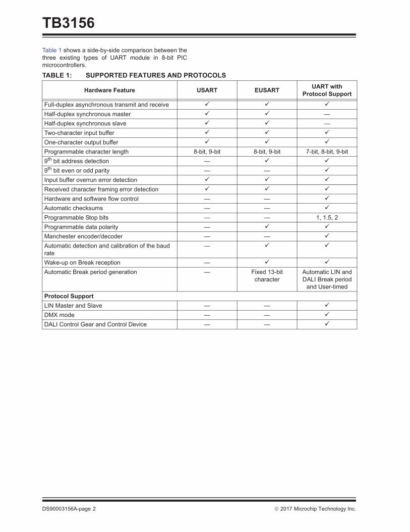
Table 1 shows a side-by-side comparison between thethree existing types of UART module in 8-bit PICmicrocontrollers.TABLE 1: SUPPORTED FEATURES AND PROTOCOLS
Hardware Feature USART EUSART UART with Protocol Support
Full-duplex asynchronous transmit and receive
Half-duplex synchronous master —Half-duplex synchronous slave —Two-character input buffer
One-character output buffer
Programmable character length 8-bit, 9-bit 8-bit, 9-bit 7-bit, 8-bit, 9-bit9th bit address detection —
9th bit even or odd parity — —
Input buffer overrun error detection
Received character framing error detection
Hardware and software flow control — —
Automatic checksums — —
Programmable Stop bits — — 1, 1.5, 2Programmable data polarity —
Manchester encoder/decoder — —
Automatic detection and calibration of the baud rate
—
Wake-up on Break reception —
Automatic Break period generation — Fixed 13-bit character
Automatic LIN and DALI Break period
and User-timedProtocol SupportLIN Master and Slave — —
DMX mode — —
DALI Control Gear and Control Device — —
DS90003156A-page 2 2017 Microchip Technology Inc.
TB3156
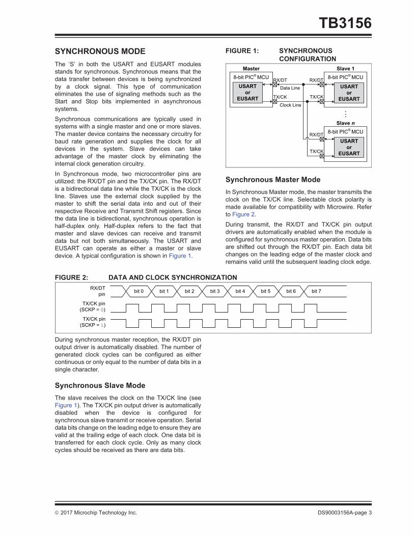
SYNCHRONOUS MODEThe ‘S’ in both the USART and EUSART modulesstands for synchronous. Synchronous means that thedata transfer between devices is being synchronizedby a clock signal. This type of communicationeliminates the use of signaling methods such as theStart and Stop bits implemented in asynchronoussystems.
Synchronous communications are typically used insystems with a single master and one or more slaves.The master device contains the necessary circuitry forbaud rate generation and supplies the clock for alldevices in the system. Slave devices can takeadvantage of the master clock by eliminating theinternal clock generation circuitry.
In Synchronous mode, two microcontroller pins areutilized: the RX/DT pin and the TX/CK pin. The RX/DTis a bidirectional data line while the TX/CK is the clockline. Slaves use the external clock supplied by themaster to shift the serial data into and out of theirrespective Receive and Transmit Shift registers. Sincethe data line is bidirectional, synchronous operation ishalf-duplex only. Half-duplex refers to the fact thatmaster and slave devices can receive and transmitdata but not both simultaneously. The USART andEUSART can operate as either a master or slavedevice. A typical configuration is shown in Figure 1.
FIGURE 1: SYNCHRONOUS CONFIGURATION
Synchronous Master ModeIn Synchronous Master mode, the master transmits theclock on the TX/CK line. Selectable clock polarity ismade available for compatibility with Microwire. Referto Figure 2.
During transmit, the RX/DT and TX/CK pin outputdrivers are automatically enabled when the module isconfigured for synchronous master operation. Data bitsare shifted out through the RX/DT pin. Each data bitchanges on the leading edge of the master clock andremains valid until the subsequent leading clock edge.
FIGURE 2: DATA AND CLOCK SYNCHRONIZATION
During synchronous master reception, the RX/DT pinoutput driver is automatically disabled. The number ofgenerated clock cycles can be configured as eithercontinuous or only equal to the number of data bits in asingle character.
Synchronous Slave ModeThe slave receives the clock on the TX/CK line (seeFigure 1). The TX/CK pin output driver is automaticallydisabled when the device is configured forsynchronous slave transmit or receive operation. Serialdata bits change on the leading edge to ensure they arevalid at the trailing edge of each clock. One data bit istransferred for each clock cycle. Only as many clockcycles should be received as there are data bits.
8-bit PIC®
MCU
USARTor
EUSART
RX/DT
TX/CK
8-bit PIC®
MCU
USARTor
EUSART
RX/DT
Master Slave 1
TX/CK
Data Line
Clock Line
8-bit PIC®
MCU
USARTor
EUSART
RX/DT
Slave n
TX/CK
•••
bit 0 bit 1 bit 2 bit 3 bit 4 bit 5 bit 6 bit 7RX/DT
pin
TX/CK pin
(SCKP = 0)
TX/CK pin
(SCKP = 1)
2017 Microchip Technology Inc. DS90003156A-page 3
TB3156
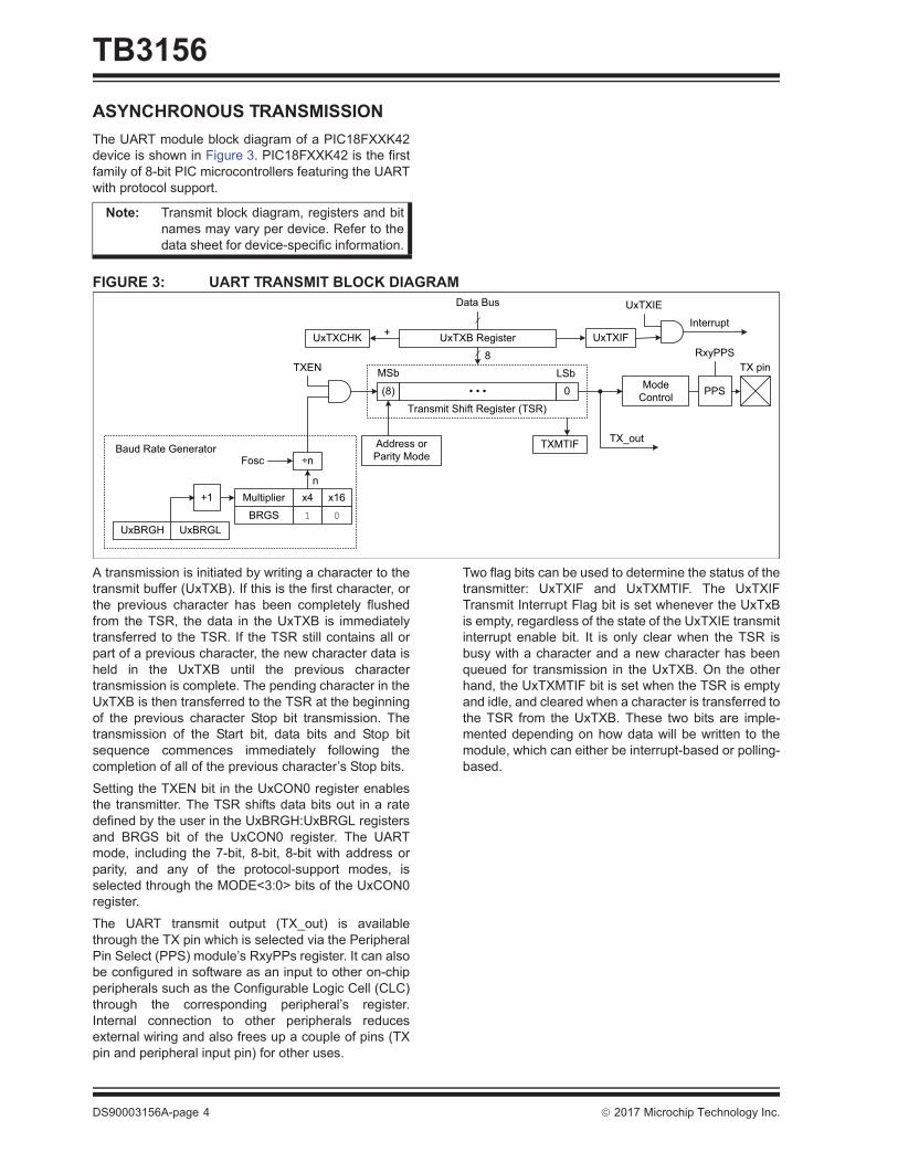
ASYNCHRONOUS TRANSMISSIONThe UART module block diagram of a PIC18FXXK42device is shown in Figure 3. PIC18FXXK42 is the firstfamily of 8-bit PIC microcontrollers featuring the UARTwith protocol support.
FIGURE 3: UART TRANSMIT BLOCK DIAGRAM
A transmission is initiated by writing a character to thetransmit buffer (UxTXB). If this is the first character, orthe previous character has been completely flushedfrom the TSR, the data in the UxTXB is immediatelytransferred to the TSR. If the TSR still contains all orpart of a previous character, the new character data isheld in the UxTXB until the previous charactertransmission is complete. The pending character in theUxTXB is then transferred to the TSR at the beginningof the previous character Stop bit transmission. Thetransmission of the Start bit, data bits and Stop bitsequence commences immediately following thecompletion of all of the previous character’s Stop bits.
Setting the TXEN bit in the UxCON0 register enablesthe transmitter. The TSR shifts data bits out in a ratedefined by the user in the UxBRGH:UxBRGL registersand BRGS bit of the UxCON0 register. The UARTmode, including the 7-bit, 8-bit, 8-bit with address orparity, and any of the protocol-support modes, isselected through the MODE<3:0> bits of the UxCON0register.
The UART transmit output (TX_out) is availablethrough the TX pin which is selected via the PeripheralPin Select (PPS) module’s RxyPPs register. It can alsobe configured in software as an input to other on-chipperipherals such as the Configurable Logic Cell (CLC)through the corresponding peripheral’s register.Internal connection to other peripherals reducesexternal wiring and also frees up a couple of pins (TXpin and peripheral input pin) for other uses.
Two flag bits can be used to determine the status of thetransmitter: UxTXIF and UxTXMTIF. The UxTXIFTransmit Interrupt Flag bit is set whenever the UxTxBis empty, regardless of the state of the UxTXIE transmitinterrupt enable bit. It is only clear when the TSR isbusy with a character and a new character has beenqueued for transmission in the UxTXB. On the otherhand, the UxTXMTIF bit is set when the TSR is emptyand idle, and cleared when a character is transferred tothe TSR from the UxTXB. These two bits are imple-mented depending on how data will be written to themodule, which can either be interrupt-based or polling-based.
Note: Transmit block diagram, registers and bitnames may vary per device. Refer to thedata sheet for device-specific information.
UxTXB Register
• • •
Transmit Shift Register (TSR)
(8) 0
MSb LSb
Data Bus
UxTXIF
UxTXIE
Interrupt
Mode
ControlPPS
RxyPPS
TX pinTXEN
UxBRGH UxBRGL
BRGS
Multiplier x4 x16
1 0+1
÷nFoscBaud Rate Generator
Address or
Parity Mode
TXMTIFTX_out
UxTXCHK
8
+
n
DS90003156A-page 4 2017 Microchip Technology Inc.
TB3156
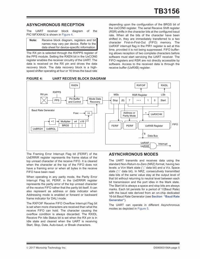
ASYNCHRONOUS RECEPTIONThe UART receiver block diagram of thePIC18FXXK42 is shown in Figure 4.
The RX pin is selected through the RXPPS register ofthe PPS module. Setting the RXEN bit in the UxCON0register enables the receiver circuitry of the UART. Thedata is received on the RX pin and drives the datarecovery block. The data recovery block is a high-speed shifter operating at four or 16 times the baud rate
depending upon the configuration of the BRGS bit ofthe UxCON0 register. The serial Receive Shift register(RSR) shifts in the character bits at the configured baudrate. When all the bits of the character have beenshifted in, they are immediately transferred to a twocharacter First-in-First-Out (FIFO) memory. TheUxRXIF interrupt flag in the PIR1 register is set at thistime, provided it is not being suppressed. FIFO buffer-ing allows reception of two complete characters beforesoftware must start servicing the UART receiver. TheFIFO registers and RSR are not directly accessible bysoftware. Access to the received data is through thereceive buffer (UxRXB) register.
FIGURE 4: UART RECEIVE BLOCK DIAGRAM
The Framing Error Interrupt Flag bit (FERIF) of theUxERRIR register represents the frame status of thetop unread character of the receive FIFO. It is clearedwhen the character at the top of the FIFO does nothave a framing error or when all bytes in the receiveFIFO have been read.
When operating in any parity mode, the Parity ErrorInterrupt Flag bit, PERIF, in the UxERRIR registerrepresents the parity error of the top unread characterof the receive FIFO rather that the parity bit itself. It canalso represent as address or data indicator whenAddressing mode is enabled or forward or backwardframe indicator for DALI mode.
The RXFOIF Receive FIFO Overflow Interrupt Flag bitis set when more characters are received than what thereceive FIFO can hold. The character causing theoverflow condition is always discarded. The RXIDLReceive Pin Idle Status bit is set when the RX pin is inIdle state and cleared when the UART is receivingStart, Stop, Data, Auto-baud, or Break characters.
ASYNCHRONOUS MODESThe UART transmits and receives data using thestandard Non-Return-to-Zero (NRZ) format, having twolevels: a VOH Mark state (‘1’ data bit) and a VOL Spacestate (‘0’ data bit). In NRZ, consecutively transmitteddata bits of the same value stay at the output level ofthat bit without returning to neutral level between eachbit transmission and the port idles in the Mark state.The Start bit is always a space and stop bits are alwaysmarks. Each bit persists for a period of 1/(Baud Rate)with the baud rate derived from an on-chip dedicated16-bit Baud Rate Generator (see Section “Baud RateGenerator”).
The UART can operate in different Asynchronousmodes as depicted in Figure 5.
Note: Receive block diagram, registers and bitnames may vary per device. Refer to thedata sheet for device-specific information.
UxBRGH UxBRGL
BRGS
Multiplier x4 x16
1 0+1
÷nFosc
Baud Rate Generator
Mode Data
Recovery
Pin Buffer
and ControlPPS
RX pin
Stop
RXPPS
RXEN
(8) • • • 1 0 Start
Address or
Parity Mode
UxRXB RegisterPERIFFERIF
RSR Register LSbMSb
RXFOIF RXIDL
8Data Bus
UxRXIF
UxRXIEInterrupt
FIFO
n
7
UxRXCHK+
2017 Microchip Technology Inc. DS90003156A-page 5
TB3156
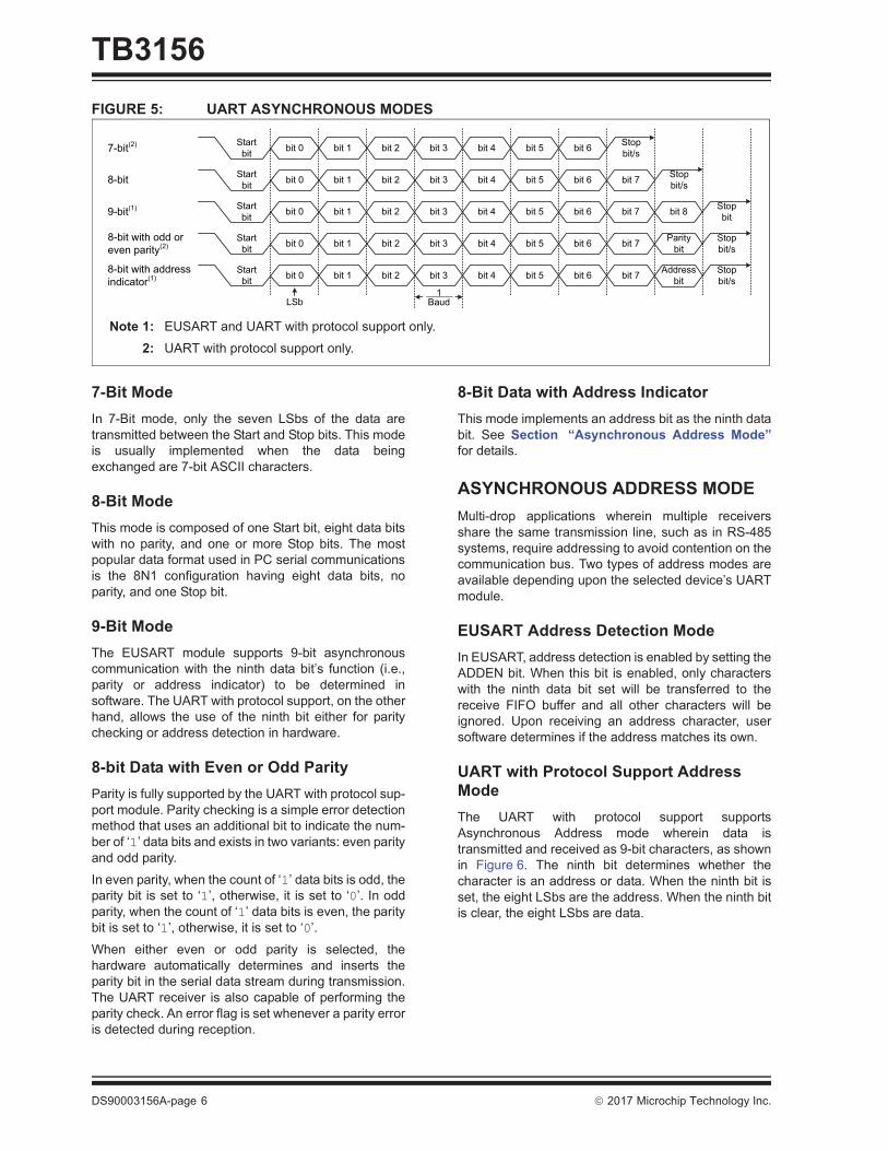
FIGURE 5: UART ASYNCHRONOUS MODES7-Bit ModeIn 7-Bit mode, only the seven LSbs of the data aretransmitted between the Start and Stop bits. This modeis usually implemented when the data beingexchanged are 7-bit ASCII characters.
8-Bit ModeThis mode is composed of one Start bit, eight data bitswith no parity, and one or more Stop bits. The mostpopular data format used in PC serial communicationsis the 8N1 configuration having eight data bits, noparity, and one Stop bit.
9-Bit ModeThe EUSART module supports 9-bit asynchronouscommunication with the ninth data bit’s function (i.e.,parity or address indicator) to be determined insoftware. The UART with protocol support, on the otherhand, allows the use of the ninth bit either for paritychecking or address detection in hardware.
8-bit Data with Even or Odd ParityParity is fully supported by the UART with protocol sup-port module. Parity checking is a simple error detectionmethod that uses an additional bit to indicate the num-ber of ‘1’ data bits and exists in two variants: even parityand odd parity.
In even parity, when the count of ‘1’ data bits is odd, theparity bit is set to ‘1’, otherwise, it is set to ‘0’. In oddparity, when the count of ‘1’ data bits is even, the paritybit is set to ‘1’, otherwise, it is set to ‘0’.
When either even or odd parity is selected, thehardware automatically determines and inserts theparity bit in the serial data stream during transmission.The UART receiver is also capable of performing theparity check. An error flag is set whenever a parity erroris detected during reception.
8-Bit Data with Address IndicatorThis mode implements an address bit as the ninth databit. See Section “Asynchronous Address Mode”for details.
ASYNCHRONOUS ADDRESS MODEMulti-drop applications wherein multiple receiversshare the same transmission line, such as in RS-485systems, require addressing to avoid contention on thecommunication bus. Two types of address modes areavailable depending upon the selected device’s UARTmodule.
EUSART Address Detection ModeIn EUSART, address detection is enabled by setting theADDEN bit. When this bit is enabled, only characterswith the ninth data bit set will be transferred to thereceive FIFO buffer and all other characters will beignored. Upon receiving an address character, usersoftware determines if the address matches its own.
UART with Protocol Support Address ModeThe UART with protocol support supportsAsynchronous Address mode wherein data istransmitted and received as 9-bit characters, as shownin Figure 6. The ninth bit determines whether thecharacter is an address or data. When the ninth bit isset, the eight LSbs are the address. When the ninth bitis clear, the eight LSbs are data.
Note 1: EUSART and UART with protocol support only.
2: UART with protocol support only.
bit 0 bit 1 bit 2 bit 3 bit 4 bit 5 bit 6 bit 7Start
bit
Stop
bit/s
bit 0 bit 1 bit 2 bit 3 bit 4 bit 5 bit 6 bit 7Start
bit
Parity
bit
Stop
bit/s
bit 0 bit 1 bit 2 bit 3 bit 4 bit 5 bit 6 bit 7Start
bit
Address
bit
Stop
bit/s
bit 0 bit 1 bit 2 bit 3 bit 4 bit 5 bit 6Start
bit
Stop
bit/s7-bit
(2)
8-bit
8-bit with odd or
even parity(2)
8-bit with address
indicator(1)
LSb1
Baud
bit 0 bit 1 bit 2 bit 3 bit 4 bit 5 bit 6 bit 7Start
bitbit 8
Stop
bit9-bit
(1)
DS90003156A-page 6 2017 Microchip Technology Inc.
TB3156
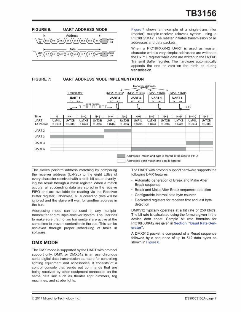
FIGURE 6: UART ADDRESS MODE Figure 7 shows an example of a single-transmitter(master) multiple-receiver (slaves) system using aPIC18F25K42. The master initiates transmission of alladdresses and data packets.
When a PIC18FXXK42 UART is used as master,character write is very simple: addresses are written tothe UxP1L register while data are written to the UxTXBTransmit Buffer register. The hardware automaticallyappends the one or zero on the ninth bit duringtransmission.
FIGURE 7: UART ADDRESS MODE IMPLEMENTATION
The slaves perform address matching by comparingthe receiver address (UxP2L) to the eight LSBs ofevery character received with a ninth bit set and verify-ing the result through a mask register. When a matchoccurs, all succeeding data are stored in the receiveFIFO and are available for reading via the ReceiverBuffer register. Otherwise, all succeeding data will beignored and the slave will wait for another address inthe bus.
Addressing mode can be used in any multiple-transmitter and multiple-receiver system. The user hasto make sure that no two transmitters are active at thesame time to prevent contention in the bus. This can beachieved through proper scheduling of tasks insoftware.
DMX MODEThe DMX mode is supported by the UART with protocolsupport only. DMX, or DMX512 is an asynchronousserial digital data transmission standard for controllinglighting equipment and accessories. It consists of acontrol console that sends out commands that arebeing received by other equipment connected on thesame data link such as theater light dimmers, fogmachines, and strobe lights.
The UART with protocol support hardware supports thefollowing DMX features:
• Automatic generation of Break and Make After Break sequence
• Break and Make After Break sequence detection• Configurable internal data byte counter• Dedicated registers for receiver first and last byte
detection
DMX512 typically operates at a bit rate of 250 kbit/s.The bit rate is calculated using the formula given in thedevice data sheet. Sample bit rate formulas forPIC18FXXK42 are given in Section “Baud Rate Gen-erator”.
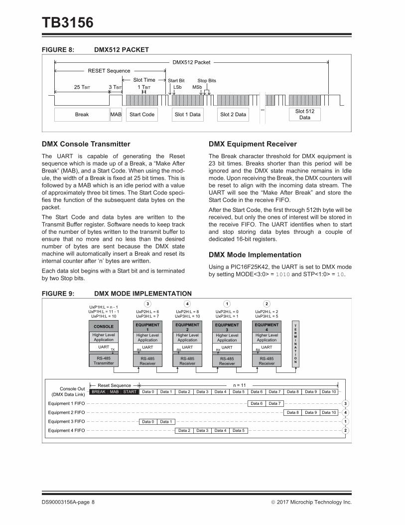
A DMX512 packet is composed of a Reset sequencefollowed by a sequence of up to 512 data bytes asshown in Figure 8.
0
1Start
bit
Stop
bit
Data
bit 0 bit 1 bit 2 bit 3 bit 4 bit 5 bit 6 bit 7
Start
bit
Stop
bitbit 0 bit 1 bit 2 bit 3 bit 4 bit 5 bit 6 bit 7
Address
UxP1L
= 0x03
UxTXB
= Data
UxTXB
= Data
UxTXB
= Data
UxP1L
= 0x02
UxTXB
= Data
UxP1L
= 0x05
UxTXB
= Data
UxTXB
= Data
UxTXB
= Data
UxP1L
= 0x04
UxTXB
= Data
UART 2
UART 3
UART 4
UART 5
UART 1
TX Packet
BUS
Addresses don’t match and data is ignored
Serial Packets
Addresses match and data is stored in the receive FIFO
N N+1 N+2 N+3 N+4 N+5 N+6 N+7 N+8 N+9 N+10 N+11
UART 1TX RX
UART 2TX RX
UART 3TX RX
UART 4TX RX
UART 5TX RX
Time
UxP2L = 0x02 UxP2L = 0x03 UxP2L = 0x04 UxP2L = 0x05
Receiver Address
Transmitter
2017 Microchip Technology Inc. DS90003156A-page 7
TB3156
FIGURE 8: DMX512 PACKETDMX Console TransmitterThe UART is capable of generating the Resetsequence which is made up of a Break, a “Make AfterBreak” (MAB), and a Start Code. When using the mod-ule, the width of a Break is fixed at 25 bit times. This isfollowed by a MAB which is an idle period with a valueof approximately three bit times. The Start Code speci-fies the function of the subsequent data bytes on thepacket.
The Start Code and data bytes are written to theTransmit Buffer register. Software needs to keep trackof the number of bytes written to the transmit buffer toensure that no more and no less than the desirednumber of bytes are sent because the DMX statemachine will automatically insert a Break and reset itsinternal counter after ‘n’ bytes are written.
Each data slot begins with a Start bit and is terminatedby two Stop bits.
DMX Equipment ReceiverThe Break character threshold for DMX equipment is23 bit times. Breaks shorter than this period will beignored and the DMX state machine remains in Idlemode. Upon receiving the Break, the DMX counters willbe reset to align with the incoming data stream. TheUART will see the “Make After Break” and store theStart Code in the receive FIFO.
After the Start Code, the first through 512th byte will bereceived, but only the ones of interest will be stored inthe receive FIFO. The UART identifies when to startand stop storing data bytes through a couple ofdedicated 16-bit registers.
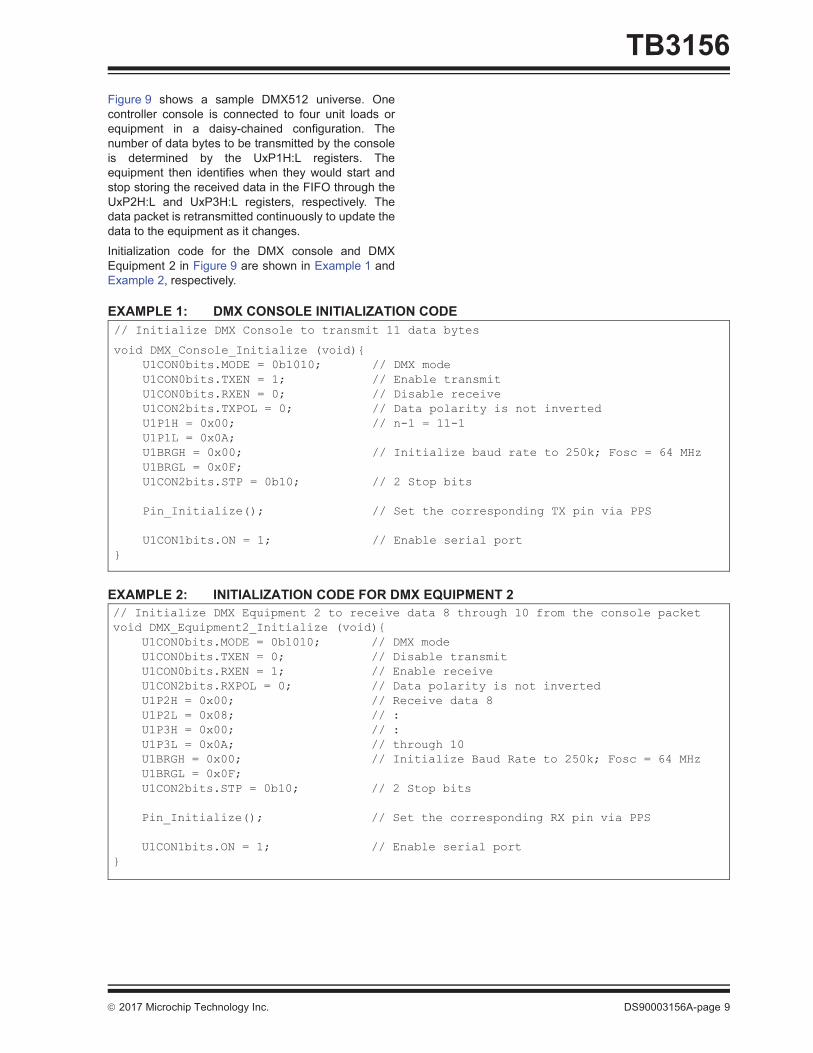
DMX Mode ImplementationUsing a PIC16F25K42, the UART is set to DMX modeby setting MODE<3:0> = 1010 and STP<1:0> = 10.
FIGURE 9: DMX MODE IMPLEMENTATION
3 TBIT
Break Start Code Slot 1 Data•••
MAB Slot 2 DataSlot 512
Data
DMX512 Packet
25 TBIT 1 TBIT LSb MSb
Stop BitsSlot Time
RESET Sequence
Start Bit
RS-485
Transmitter
Higher Level
Application
UART
CONSOLE
TX
TERMINATION
Console Out
Equipment 1 FIFO
Equipment 2 FIFO
Equipment 3 FIFO
Equipment 4 FIFO
(DMX Data Link)
Data 0 Data 1
Data 2 Data 3 Data 4 Data 5
Data 6 Data 7
Data 8 Data 9 Data 10
BREAK Data 0 Data 1 Data 2 Data 3 Data 4 Data 5 Data 6 Data 7 Data 8 Data 9 Data 10STARTMAB
UxP2H:L = 2UxP3H:L = 5
UxP2H:L = 0UxP3H:L = 1
UxP2H:L = 8UxP3H:L = 10
UxP2H:L = 6UxP3H:L = 7UxP1H:L = 10
2
23 4
1
4
3
1
n = 11Reset Sequence
UxP1H:L = 11 - 1UxP1H:L = n - 1
RS-485
Receiver
Higher Level
Application
UART
EQUIPMENT 2
RX
RS-485
Receiver
Higher Level
Application
UART
EQUIPMENT 3
RX
RS-485
Receiver
Higher Level
Application
UART
EQUIPMENT 4
RX
RS-485
Receiver
Higher Level
Application
UART
EQUIPMENT 1
RX
DS90003156A-page 8 2017 Microchip Technology Inc.
TB3156
Figure 9 shows a sample DMX512 universe. Onecontroller console is connected to four unit loads orequipment in a daisy-chained configuration. Thenumber of data bytes to be transmitted by the consoleis determined by the UxP1H:L registers. Theequipment then identifies when they would start andstop storing the received data in the FIFO through theUxP2H:L and UxP3H:L registers, respectively. Thedata packet is retransmitted continuously to update thedata to the equipment as it changes.Initialization code for the DMX console and DMXEquipment 2 in Figure 9 are shown in Example 1 andExample 2, respectively.
EXAMPLE 1: DMX CONSOLE INITIALIZATION CODE
EXAMPLE 2: INITIALIZATION CODE FOR DMX EQUIPMENT 2
// Initialize DMX Console to transmit 11 data bytes
void DMX_Console_Initialize (void){ U1CON0bits.MODE = 0b1010; // DMX mode U1CON0bits.TXEN = 1; // Enable transmit U1CON0bits.RXEN = 0; // Disable receive U1CON2bits.TXPOL = 0; // Data polarity is not inverted U1P1H = 0x00; // n-1 = 11-1 U1P1L = 0x0A; U1BRGH = 0x00; // Initialize baud rate to 250k; Fosc = 64 MHz U1BRGL = 0x0F; U1CON2bits.STP = 0b10; // 2 Stop bits
Pin_Initialize(); // Set the corresponding TX pin via PPS U1CON1bits.ON = 1; // Enable serial port}
// Initialize DMX Equipment 2 to receive data 8 through 10 from the console packetvoid DMX_Equipment2_Initialize (void){ U1CON0bits.MODE = 0b1010; // DMX mode U1CON0bits.TXEN = 0; // Disable transmit U1CON0bits.RXEN = 1; // Enable receive U1CON2bits.RXPOL = 0; // Data polarity is not inverted U1P2H = 0x00; // Receive data 8 U1P2L = 0x08; // : U1P3H = 0x00; // : U1P3L = 0x0A; // through 10 U1BRGH = 0x00; // Initialize Baud Rate to 250k; Fosc = 64 MHz U1BRGL = 0x0F; U1CON2bits.STP = 0b10; // 2 Stop bits Pin_Initialize(); // Set the corresponding RX pin via PPS U1CON1bits.ON = 1; // Enable serial port}
2017 Microchip Technology Inc. DS90003156A-page 9
TB3156
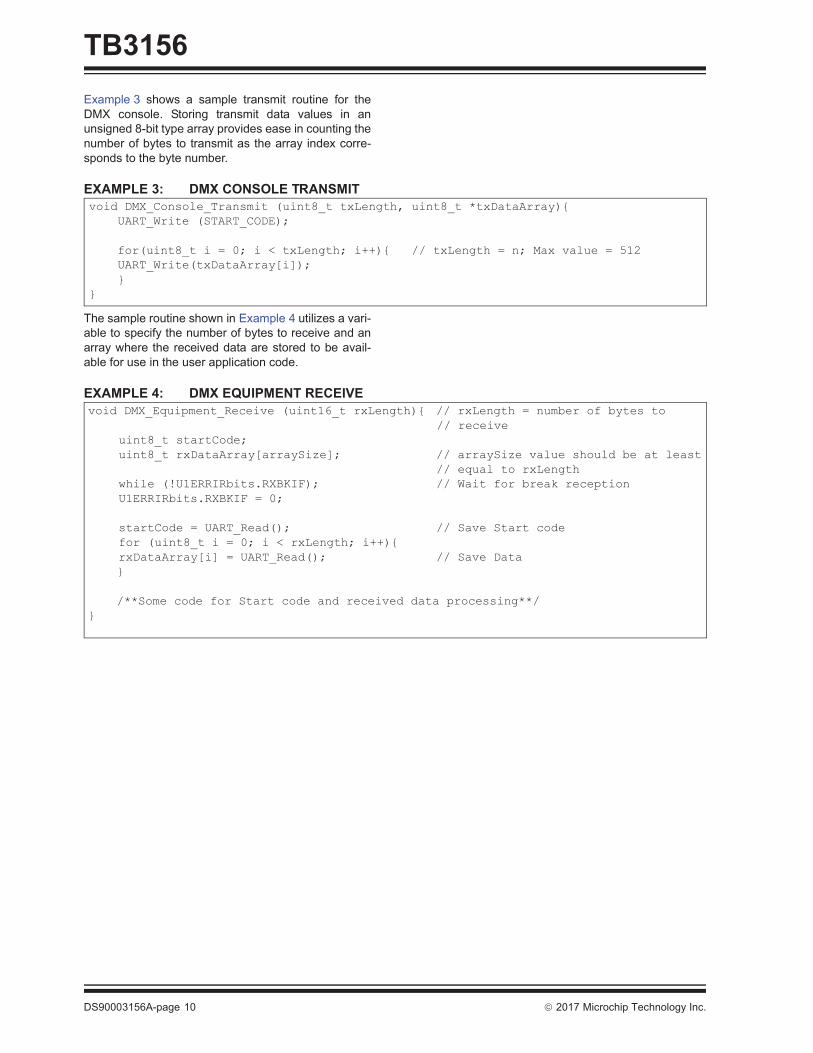
Example 3 shows a sample transmit routine for theDMX console. Storing transmit data values in anunsigned 8-bit type array provides ease in counting thenumber of bytes to transmit as the array index corre-sponds to the byte number.EXAMPLE 3: DMX CONSOLE TRANSMIT
The sample routine shown in Example 4 utilizes a vari-able to specify the number of bytes to receive and anarray where the received data are stored to be avail-able for use in the user application code.
EXAMPLE 4: DMX EQUIPMENT RECEIVE
void DMX_Console_Transmit (uint8_t txLength, uint8_t *txDataArray){ UART_Write (START_CODE); for(uint8_t i = 0; i < txLength; i++){ // txLength = n; Max value = 512 UART_Write(txDataArray[i]); }}
void DMX_Equipment_Receive (uint16_t rxLength){ // rxLength = number of bytes to // receive
uint8_t startCode;uint8_t rxDataArray[arraySize]; // arraySize value should be at least
// equal to rxLengthwhile (!U1ERRIRbits.RXBKIF); // Wait for break receptionU1ERRIRbits.RXBKIF = 0;
startCode = UART_Read(); // Save Start codefor (uint8_t i = 0; i < rxLength; i++){rxDataArray[i] = UART_Read(); // Save Data
} /**Some code for Start code and received data processing**/}
DS90003156A-page 10 2017 Microchip Technology Inc.
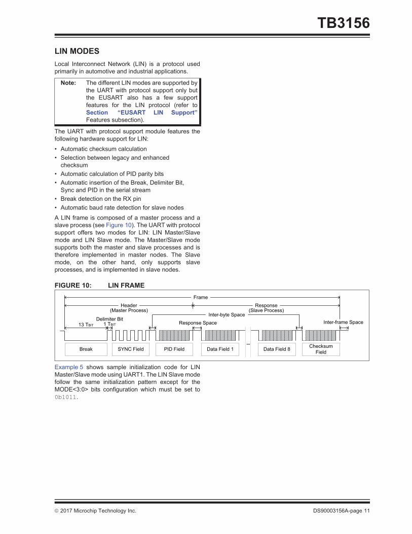
TB3156
LIN MODESLocal Interconnect Network (LIN) is a protocol usedprimarily in automotive and industrial applications.
The UART with protocol support module features thefollowing hardware support for LIN:
• Automatic checksum calculation• Selection between legacy and enhanced
checksum• Automatic calculation of PID parity bits • Automatic insertion of the Break, Delimiter Bit,
Sync and PID in the serial stream• Break detection on the RX pin• Automatic baud rate detection for slave nodes
A LIN frame is composed of a master process and aslave process (see Figure 10). The UART with protocolsupport offers two modes for LIN: LIN Master/Slavemode and LIN Slave mode. The Master/Slave modesupports both the master and slave processes and istherefore implemented in master nodes. The Slavemode, on the other hand, only supports slaveprocesses, and is implemented in slave nodes.
FIGURE 10: LIN FRAME
Example 5 shows sample initialization code for LINMaster/Slave mode using UART1. The LIN Slave modefollow the same initialization pattern except for theMODE<3:0> bits configuration which must be set to0b1011.
Note: The different LIN modes are supported bythe UART with protocol support only butthe EUSART also has a few supportfeatures for the LIN protocol (refer toSection “EUSART LIN Support”Features subsection).
13 TBIT 1 TBIT
PID Field
Inter-byte Space
Header Response
Frame
Break SYNC Field Data Field 1•••
Data Field 8Checksum
Field
Response SpaceDelimiter Bit
Inter-frame Space
(Master Process) (Slave Process)
2017 Microchip Technology Inc. DS90003156A-page 11
TB3156
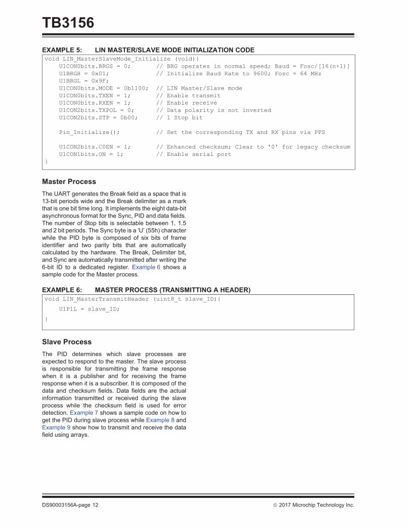
EXAMPLE 5: LIN MASTER/SLAVE MODE INITIALIZATION CODEMaster ProcessThe UART generates the Break field as a space that is13-bit periods wide and the Break delimiter as a markthat is one bit time long. It implements the eight data-bitasynchronous format for the Sync, PID and data fields.The number of Stop bits is selectable between 1, 1.5and 2 bit periods. The Sync byte is a ‘U’ (55h) characterwhile the PID byte is composed of six bits of frameidentifier and two parity bits that are automaticallycalculated by the hardware. The Break, Delimiter bit,and Sync are automatically transmitted after writing the6-bit ID to a dedicated register. Example 6 shows asample code for the Master process.
EXAMPLE 6: MASTER PROCESS (TRANSMITTING A HEADER)
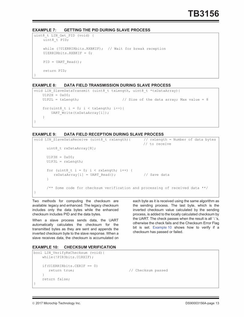
Slave ProcessThe PID determines which slave processes areexpected to respond to the master. The slave processis responsible for transmitting the frame responsewhen it is a publisher and for receiving the frameresponse when it is a subscriber. It is composed of thedata and checksum fields. Data fields are the actualinformation transmitted or received during the slaveprocess while the checksum field is used for errordetection. Example 7 shows a sample code on how toget the PID during slave process while Example 8 andExample 9 show how to transmit and receive the datafield using arrays.
void LIN_MasterSlaveMode_Initialize (void){ U1CON0bits.BRGS = 0; // BRG operates in normal speed; Baud = Fosc/[16(n+1)] U1BRGH = 0x01; // Initialize Baud Rate to 9600; Fosc = 64 MHz U1BRGL = 0x9F; U1CON0bits.MODE = 0b1100; // LIN Master/Slave mode U1CON0bits.TXEN = 1; // Enable transmit U1CON0bits.RXEN = 1; // Enable receive U1CON2bits.TXPOL = 0; // Data polarity is not inverted U1CON2bits.STP = 0b00; // 1 Stop bit Pin_Initialize(); // Set the corresponding TX and RX pins via PPS U1CON2bits.C0EN = 1; // Enhanced checksum; Clear to '0' for legacy checksum U1CON1bits.ON = 1; // Enable serial port}
void LIN_MasterTransmitHeader (uint8_t slave_ID){
U1P1L = slave_ID;
}
DS90003156A-page 12 2017 Microchip Technology Inc.
TB3156
EXAMPLE 7: GETTING THE PID DURING SLAVE PROCESSEXAMPLE 8: DATA FIELD TRANSMISSION DURING SLAVE PROCESS
EXAMPLE 9: DATA FIELD RECEPTION DURING SLAVE PROCESS
Two methods for computing the checksum areavailable: legacy and enhanced. The legacy checksumincludes only the data bytes while the enhancedchecksum includes PID and the data bytes.
When a slave process sends data, the UARTautomatically calculates the checksum for thetransmitted bytes as they are sent and appends theinverted checksum byte to the slave response. When aslave receives data, the checksum is accumulated on
each byte as it is received using the same algorithm asthe sending process. The last byte, which is theinverted checksum value calculated by the sendingprocess, is added to the locally calculated checksum bythe UART. The check passes when the result is all ‘1’s,otherwise the check fails and the Checksum Error Flagbit is set. Example 10 shows how to verify if achecksum has passed or failed.
EXAMPLE 10: CHECKSUM VERIFICATION
uint8_t LIN_Get_PID (void) {uint8_t PID;
while (!U1ERRIRbits.RXBKIF); // Wait for break receptionU1ERRIRbits.RXBKIF = 0;
PID = UART_Read();
return PID;}
void LIN_SlaveDataTransmit (uint8_t txLength, uint8_t *txDataArray){ U1P2H = 0x00; U1P2L = txLength; // Size of the data array; Max value = 8 for(uint8_t i = 0; i < txLength; i++){ UART_Write(txDataArray[i]); }}
void LIN_SlaveDataReceive (uint8_t rxLength){ // rxLength = Number of data bytes // to receive
uint8_t rxDataArray[8];
U1P3H = 0x00;U1P3L = rxLength;
for (uint8_t i = 0; i < rxLength; i++) {rxDataArray[i] = UART_Read(); // Save data
}
/** Some code for checksum verification and processing of received data **/}
bool LIN_VerifyRxChecksum (void){ while(!PIR3bits.U1RXIF);
if(U1ERRIRbits.CERIF == 0) return true; // Checksum passed } return false;}
2017 Microchip Technology Inc. DS90003156A-page 13
TB3156
The checksum method, number of data bytes, andwhether to send or receive data in slave process, isdefined by software according to the PID. The inter-byte period, timeout and frame period are timed bysoftware using a means other than the UART. On-chiphardware timers such as Timer0/1/2 can be used forthis purpose.EUSART LIN SupportThe EUSART module of enhanced mid-range and highend PIC MCUs supports a fixed 13-bit Breaktransmission and wake-up on Break detection. Theother tasks are left for the user to determine insoftware. Microchip’s MPLAB® Code Configurator(MCC) LIN module allows the user to create scheduletables, and select checksum type and hardware timersthrough an easy to use GUI. It supports majority ofdevices with EUSART and is capable of generatingsoftware routines necessary for rapid prototypingpurposes. For more information, refer to AN2059, “LINBasics and Implementation of the MCC LIN StackLibrary on 8-bit PIC® Microcontrollers”.
DALI MODE
Digital Addressable Lighting Interface (DALI) is aprotocol used in digital lighting control in large buildingssuch as offices and factories. DALI support is onlyavailable in the UART with protocol support module. Itprovides the following features for DALI:
• Selectable modes between control device and control gear
• Manchester encoding• Most Significant bit first• No Stop periods between back-to-back bytes• Two Stop bits transmission and detection• Configurable forward and back wait period in half-
bit steps• Forward/Back Frame detection threshold delimiter
configurable in half-bit steps• Automatic transmission of back frame at the end
of wait time
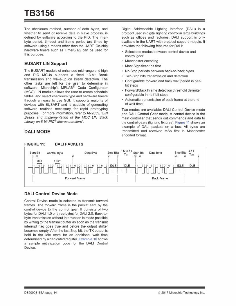
Two modes are available: DALI Control Device modeand DALI Control Gear mode. A control device is themain controller that sends out commands and data tothe control gears (lighting fixtures). Figure 11 shows anexample of DALI packets on a bus. All bytes aretransmitted and received MSb first in Manchesterencoded format.
FIGURE 11: DALI PACKETS
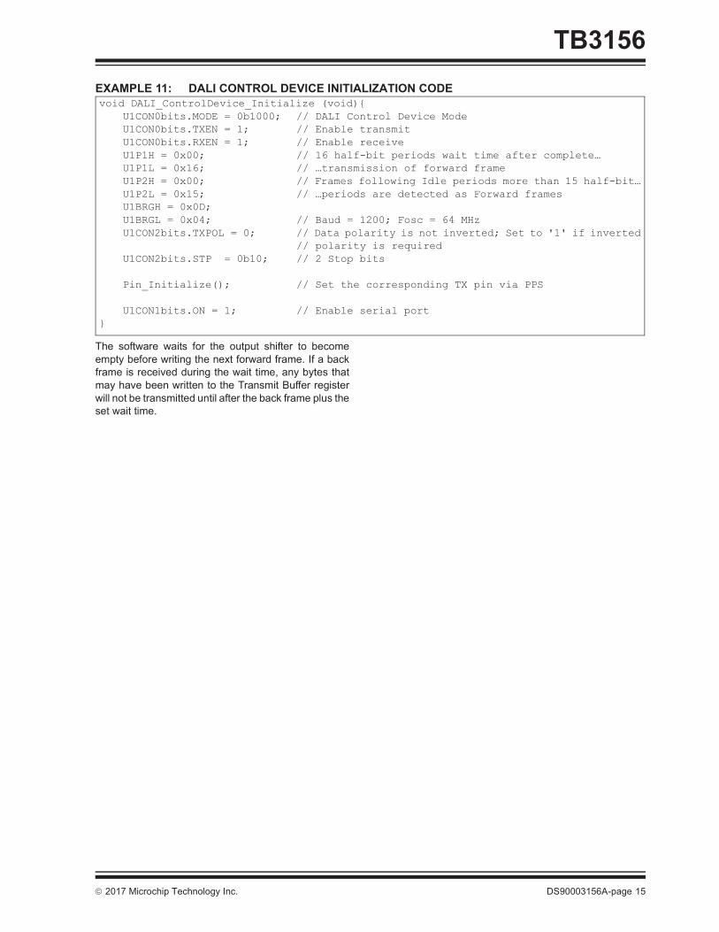
DALI Control Device ModeControl Device mode is selected to transmit forwardframes. The forward frame is the packet sent by thecontrol device to the control gear. It consists of twobytes for DALI 1.0 or three bytes for DALI 2.0. Back-to-byte transmission without interruption is made possibleby writing to the transmit buffer as soon as the transmitinterrupt flag goes true and before the output shifterbecomes empty. After the last Stop bit, the TX output isheld in the Idle state for an additional wait timedetermined by a dedicated register. Example 10 showsa sample initialization code for the DALI ControlDevice.
IDLEIDLE1 0 0 1 0 1 0 1 1 0 0 1 1 0 1 0 0
Forward Frame
Start Bit Stop BitsData ByteControl Byte
IDLE
3.5 to 11
TBIT
IDLE0 0 0 1 1 0 0 11
Back Frame
MSb 1 TBIT
Data Byte>11
TBITStop BitsStart Bit
DS90003156A-page 14 2017 Microchip Technology Inc.
TB3156
EXAMPLE 11: DALI CONTROL DEVICE INITIALIZATION CODEThe software waits for the output shifter to becomeempty before writing the next forward frame. If a backframe is received during the wait time, any bytes thatmay have been written to the Transmit Buffer registerwill not be transmitted until after the back frame plus theset wait time.
void DALI_ControlDevice_Initialize (void){U1CON0bits.MODE = 0b1000; // DALI Control Device ModeU1CON0bits.TXEN = 1; // Enable transmitU1CON0bits.RXEN = 1; // Enable receiveU1P1H = 0x00; // 16 half-bit periods wait time after complete… U1P1L = 0x16; // …transmission of forward frameU1P2H = 0x00; // Frames following Idle periods more than 15 half-bit…U1P2L = 0x15; // …periods are detected as Forward framesU1BRGH = 0x0D;U1BRGL = 0x04; // Baud = 1200; Fosc = 64 MHzU1CON2bits.TXPOL = 0; // Data polarity is not inverted; Set to '1' if inverted
// polarity is requiredU1CON2bits.STP = 0b10; // 2 Stop bits
Pin_Initialize(); // Set the corresponding TX pin via PPS
U1CON1bits.ON = 1; // Enable serial port
}
2017 Microchip Technology Inc. DS90003156A-page 15
TB3156
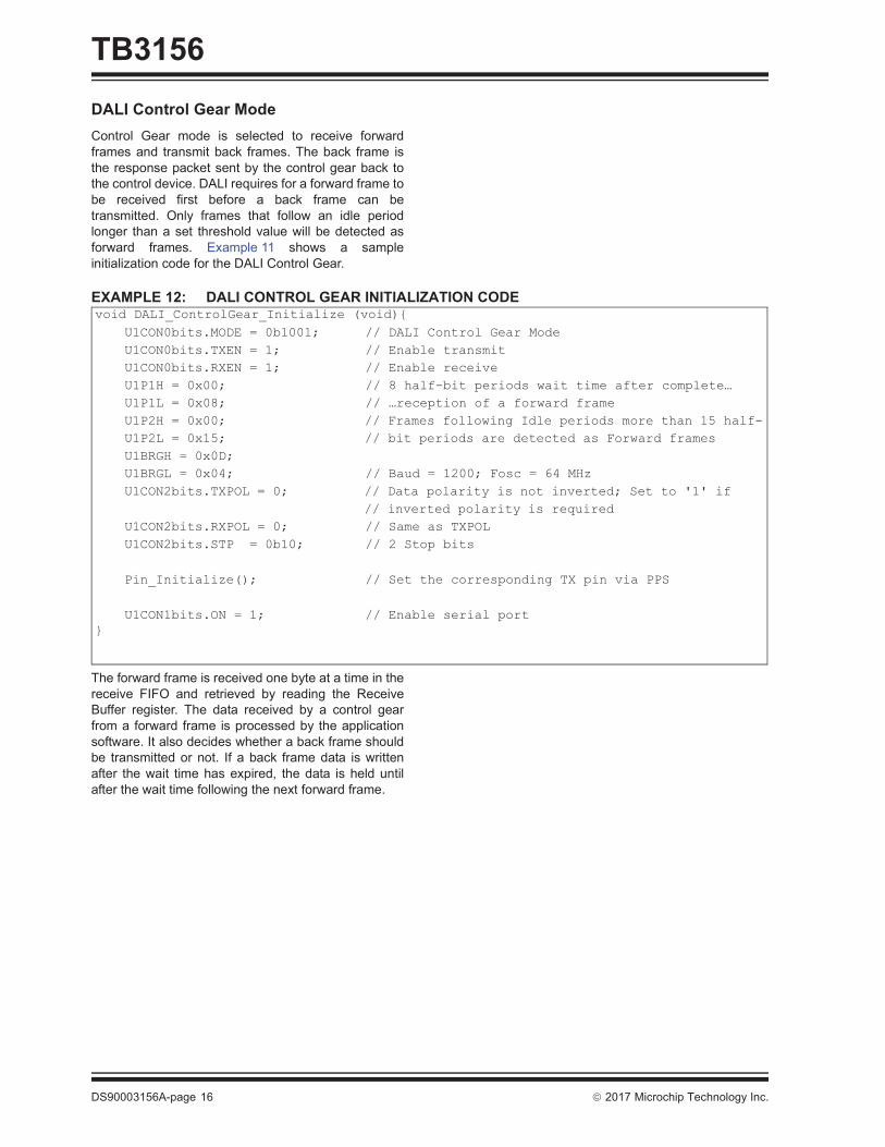
DALI Control Gear ModeControl Gear mode is selected to receive forwardframes and transmit back frames. The back frame isthe response packet sent by the control gear back tothe control device. DALI requires for a forward frame tobe received first before a back frame can betransmitted. Only frames that follow an idle periodlonger than a set threshold value will be detected asforward frames. Example 11 shows a sampleinitialization code for the DALI Control Gear.EXAMPLE 12: DALI CONTROL GEAR INITIALIZATION CODE
The forward frame is received one byte at a time in thereceive FIFO and retrieved by reading the ReceiveBuffer register. The data received by a control gearfrom a forward frame is processed by the applicationsoftware. It also decides whether a back frame shouldbe transmitted or not. If a back frame data is writtenafter the wait time has expired, the data is held untilafter the wait time following the next forward frame.
void DALI_ControlGear_Initialize (void){
U1CON0bits.MODE = 0b1001; // DALI Control Gear Mode
U1CON0bits.TXEN = 1; // Enable transmit
U1CON0bits.RXEN = 1; // Enable receive
U1P1H = 0x00; // 8 half-bit periods wait time after complete…
U1P1L = 0x08; // …reception of a forward frame
U1P2H = 0x00; // Frames following Idle periods more than 15 half-
U1P2L = 0x15; // bit periods are detected as Forward frames
U1BRGH = 0x0D;
U1BRGL = 0x04; // Baud = 1200; Fosc = 64 MHz
U1CON2bits.TXPOL = 0; // Data polarity is not inverted; Set to '1' if
// inverted polarity is required
U1CON2bits.RXPOL = 0; // Same as TXPOL
U1CON2bits.STP = 0b10; // 2 Stop bits
Pin_Initialize(); // Set the corresponding TX pin via PPS
U1CON1bits.ON = 1; // Enable serial port}
DS90003156A-page 16 2017 Microchip Technology Inc.
TB3156
GENERAL PURPOSE MANCHESTERGeneral purpose Manchester is a subset of the DALImode. It maintains all aspects of DALI mode. The onlydifference is that the wait time is set to zero. This allowsfull and half-duplex operation because writes are notheld waiting for a receive operation to complete.
BAUD RATE GENERATORThe Baud Rate Generator (BRG) is an 8-bit or 16-bittimer that is dedicated to support both the Synchronousand Asynchronous modes of operation.
The UART module allows selection between normaland high baud rate range. The high baud rate range isintended to extend the baud rate range when thedesired baud rate is not possible otherwise. The normalbaud rate range is recommended when the desiredbaud rate is achievable with either range.
Calculation of baud rate differs from each type of UARTmodule and the configured speed. Baud rate formulasare usually given on the device data sheet. Table 2shows the baud rate formulas for the PIC18FXXK42.
The calculated baud rate is stored in a pair of 8-bitregisters.
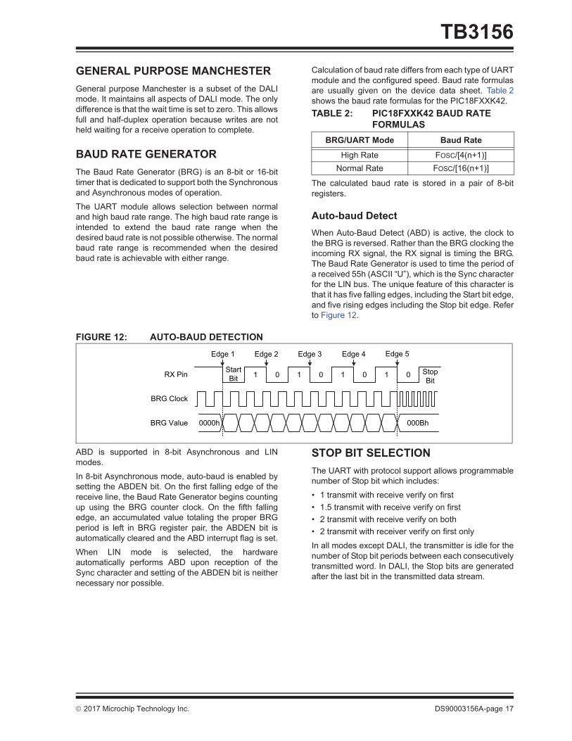
Auto-baud DetectWhen Auto-Baud Detect (ABD) is active, the clock tothe BRG is reversed. Rather than the BRG clocking theincoming RX signal, the RX signal is timing the BRG.The Baud Rate Generator is used to time the period ofa received 55h (ASCII “U”), which is the Sync characterfor the LIN bus. The unique feature of this character isthat it has five falling edges, including the Start bit edge,and five rising edges including the Stop bit edge. Referto Figure 12.
FIGURE 12: AUTO-BAUD DETECTION
ABD is supported in 8-bit Asynchronous and LINmodes.
In 8-bit Asynchronous mode, auto-baud is enabled bysetting the ABDEN bit. On the first falling edge of thereceive line, the Baud Rate Generator begins countingup using the BRG counter clock. On the fifth fallingedge, an accumulated value totaling the proper BRGperiod is left in BRG register pair, the ABDEN bit isautomatically cleared and the ABD interrupt flag is set.
When LIN mode is selected, the hardwareautomatically performs ABD upon reception of theSync character and setting of the ABDEN bit is neithernecessary nor possible.
STOP BIT SELECTIONThe UART with protocol support allows programmablenumber of Stop bit which includes:
• 1 transmit with receive verify on first• 1.5 transmit with receive verify on first• 2 transmit with receive verify on both• 2 transmit with receiver verify on first only
In all modes except DALI, the transmitter is idle for thenumber of Stop bit periods between each consecutivelytransmitted word. In DALI, the Stop bits are generatedafter the last bit in the transmitted data stream.
TABLE 2: PIC18FXXK42 BAUD RATE FORMULAS
BRG/UART Mode Baud Rate
High Rate FOSC/[4(n+1)]Normal Rate FOSC/[16(n+1)]
1 0 1 0 1 0 1 0Start
BitStop
Bit
0000h
RX Pin
Edge 2 Edge 3 Edge 4 Edge 5
BRG Clock
BRG Value 000Bh
Edge 1
2017 Microchip Technology Inc. DS90003156A-page 17
TB3156
AUTOMATIC CHECKSUM CALCULATIONThe UART with protocol support has transmit andreceive checksum adders. When enabled, the addersaccumulate every byte that is transmitted or received.The accumulated sum includes the carry of the additionand is stored in a checksum register.
Software is responsible for clearing the checksumregisters before a transaction and performing the checkat the end of transaction. In LIN mode, automaticchecksum calculation is always enabled and thehardware clears and checks the sums automatically.
FLOW CONTROLThe UART with protocol support features bothhardware and software flow control selectable throughthe handshake flow control bits. Flow control reducesthe risk of data loss and prevents buffer overruns bysignaling when a device is ready to transmit or receivedata.
Hardware Flow ControlHardware flow control uses a couple of microcontrollerpins in addition to the TX and RX pins. The RS-232signal names for these are RTS (Request to Send) andCTS (Clear to Send). A typical configuration betweentwo Data Terminal Equipment (DTE) is shown inFigure 13. Each DTE uses the RTS to output if it isready to accept new data and read CTS to see if it isallowed to send data to the other device. Both lines arelow true and are configurable through the PPS module.
FIGURE 13: HARDWARE FLOW CONTROL CONFIGURATION
The UART receiving data asserts the RTS output lowwhen the input FIFO is empty. When a character isreceived, the RTS output goes high until the receivebuffer is read to free up both FIFO locations.
The UART sending data will only be able to transmitwhen the CTS input is detected low. When the CTSinput goes high after a byte has started to transmit, thetransmission will complete normally. The receivingUART accommodates this by accepting the characterin the second FIFO location even when the CTS inputis high.
RS-485 Transceiver ControlAnother microcontroller pin may be used to control anRS-485 transceiver. The signal name for this is TXDEfor Transmit Drive Enable. This output is high when theTX output is actively sending a character and low at allother times. Hardware flow control can be used tocontrol the direction of the RS-485 transceiver. Asample configuration is shown in Figure 14. The TXDEpin is selected through the PPS module.
FIGURE 14: RS-485 CONFIGURATION
XON/XOFF Software Flow ControlXON/XOFF uses special characters to suspend andresume transmission. It requires full-duplex operationbecause the transmitter must be able to receive thesignal to suspend transmitting while the transmission isin progress. The UART uses 13h for XOFF and 11h forXON.
The transmitter defaults to XON, or transmitter enabled.When an XOFF character is received, the transmitterstops transmitting after completing the characteractively being transmitted. The transmitter remainsdisabled until an XON character is received.
On-chip software flow control allows reliable dataexchange while reducing the cost of using additionalpins required in hardware control. However, it has adrawback of latency since XON and XOFF charactersare also inserted in the serial stream.
TX
CTS
RX
RTS
DTE
UART
RX
RTS
DTE
UARTTX
CTS
8-bit PIC®
MCU
UART
RX
TXDE
SN75716R
RE
DE
DTX
A
B
4k7
4k7
VCC
DS90003156A-page 18 2017 Microchip Technology Inc.
TB3156
OPERATION WITH OTHER PERIPHERALSThis section provides a few sample implementations ofthe UART with other on-chip peripherals.
RX/TX Activity Timeout Using HLTThe Hardware Limit Timer (HLT) of even numberedtimer modules can be used to monitor the activity of theUART TX and RX lines. The TX or RX lines can be con-figured as the Reset signal source for HLT. The HLTshould be configured such that the UART activity willkeep resetting the HLT to prevent a full HLT period fromelapsing. When there has been no activity on theselected TX or RX line for longer than the HLT period,an HLT interrupt will occur signaling the timeout event.
UART Data Transfer Using DMADevices such as the PIC18FXXK42 feature an on-chipDirect Memory Access (DMA) controller. The DMAallows the UART to transfer data directly from theReceiver Buffer register to RAM or from RAM to theTransmit Buffer register, without intervention from theCPU. The UART RX and TX can also be configured totrigger an interrupt request to the DMA to start a newDMA message. Allowing the DMA to take over thememory bus during UART data transfers enables theCPU to perform other important tasks, resulting in amore efficient CPU usage and higher data throughput.
Digital Modulation Using UART and CLCSeveral UART modules support internal connection ofthe UART transmit output to the Configurable LogicCell (CLC) module. One significant implementation ofthe UART with CLC is in Data Signal Modulator (DSM).Digital modulation techniques such as On-Off Keying(OOK), Frequency Shift Keying (FSK), and Phase ShiftKeying (PSK) are supported by the DSM. The CLCuses the UART as the input data source and other sig-nal sources (e.g., System clock, LPRC, SOSC, etc.) asthe carrier signal. Refer to AN2133, “Extending PIC®
MCU Capabilities Using CLC” for detailed discussion.
CONCLUSIONThis technical brief covers the different capabilities andfeatures of the three existing varieties of UART moduleon 8-bit PIC microcontrollers. The UART with protocolsupport module was given much emphasis to helpusers understand quickly the different advanced fea-tures that are not supported by the USART andEUSART. Using this module allows designers todevelop their UART-based applications with much lesssoftware overhead in a shorter period of time.
REFERENCES• PIC18FXXK42 Data Sheet• ANSI E1.11-2008 (R2013) Standard• AN1659, “DMX512A” (DS00001659)• AN2059, “LIN Basics and Implementation of the
MCC LIN Stack Library on 8-bit PIC® Microcontrollers”
• AN1465, “Digitally Addressable Lighting Interface (DALI) Communication” (DS01465)
• AN2133, “Extending PIC® MCU Capabilities Using CLC”
2017 Microchip Technology Inc. DS90003156A-page 19
TB3156
NOTES:DS90003156A-page 20 2017 Microchip Technology Inc.
Note the following details of the code protection feature on Microchip devices:• Microchip products meet the specification contained in their particular Microchip Data Sheet.
• Microchip believes that its family of products is one of the most secure families of its kind on the market today, when used in the intended manner and under normal conditions.
• There are dishonest and possibly illegal methods used to breach the code protection feature. All of these methods, to our knowledge, require using the Microchip products in a manner outside the operating specifications contained in Microchip’s Data Sheets. Most likely, the person doing so is engaged in theft of intellectual property.
• Microchip is willing to work with the customer who is concerned about the integrity of their code.
• Neither Microchip nor any other semiconductor manufacturer can guarantee the security of their code. Code protection does not mean that we are guaranteeing the product as “unbreakable.”
Code protection is constantly evolving. We at Microchip are committed to continuously improving the code protection features of ourproducts. Attempts to break Microchip’s code protection feature may be a violation of the Digital Millennium Copyright Act. If such actsallow unauthorized access to your software or other copyrighted work, you may have a right to sue for relief under that Act.
Information contained in this publication regarding deviceapplications and the like is provided only for your convenienceand may be superseded by updates. It is your responsibility toensure that your application meets with your specifications.MICROCHIP MAKES NO REPRESENTATIONS ORWARRANTIES OF ANY KIND WHETHER EXPRESS ORIMPLIED, WRITTEN OR ORAL, STATUTORY OROTHERWISE, RELATED TO THE INFORMATION,INCLUDING BUT NOT LIMITED TO ITS CONDITION,QUALITY, PERFORMANCE, MERCHANTABILITY ORFITNESS FOR PURPOSE. Microchip disclaims all liabilityarising from this information and its use. Use of Microchipdevices in life support and/or safety applications is entirely atthe buyer’s risk, and the buyer agrees to defend, indemnify andhold harmless Microchip from any and all damages, claims,suits, or expenses resulting from such use. No licenses areconveyed, implicitly or otherwise, under any Microchipintellectual property rights unless otherwise stated.
2017 Microchip Technology Inc.
Microchip received ISO/TS-16949:2009 certification for its worldwide headquarters, design and wafer fabrication facilities in Chandler and Tempe, Arizona; Gresham, Oregon and design centers in California and India. The Company’s quality system processes and procedures are for its PIC® MCUs and dsPIC® DSCs, KEELOQ® code hopping devices, Serial EEPROMs, microperipherals, nonvolatile memory and analog products. In addition, Microchip’s quality system for the design and manufacture of development systems is ISO 9001:2000 certified.
QUALITY MANAGEMENT SYSTEM CERTIFIED BY DNV
== ISO/TS 16949 ==
TrademarksThe Microchip name and logo, the Microchip logo, AnyRate, AVR, AVR logo, AVR Freaks, BeaconThings, BitCloud, CryptoMemory, CryptoRF, dsPIC, FlashFlex, flexPWR, Heldo, JukeBlox, KEELOQ, KEELOQ logo, Kleer, LANCheck, LINK MD, maXStylus, maXTouch, MediaLB, megaAVR, MOST, MOST logo, MPLAB, OptoLyzer, PIC, picoPower, PICSTART, PIC32 logo, Prochip Designer, QTouch, RightTouch, SAM-BA, SpyNIC, SST, SST Logo, SuperFlash, tinyAVR, UNI/O, and XMEGA are registered trademarks of Microchip Technology Incorporated in the U.S.A. and other countries.
ClockWorks, The Embedded Control Solutions Company, EtherSynch, Hyper Speed Control, HyperLight Load, IntelliMOS, mTouch, Precision Edge, and Quiet-Wire are registered trademarks of Microchip Technology Incorporated in the U.S.A.
Adjacent Key Suppression, AKS, Analog-for-the-Digital Age, Any Capacitor, AnyIn, AnyOut, BodyCom, chipKIT, chipKIT logo, CodeGuard, CryptoAuthentication, CryptoCompanion, CryptoController, dsPICDEM, dsPICDEM.net, Dynamic Average Matching, DAM, ECAN, EtherGREEN, In-Circuit Serial Programming, ICSP, Inter-Chip Connectivity, JitterBlocker, KleerNet, KleerNet logo, Mindi, MiWi, motorBench, MPASM, MPF, MPLAB Certified logo, MPLIB, MPLINK, MultiTRAK, NetDetach, Omniscient Code Generation, PICDEM, PICDEM.net, PICkit, PICtail, PureSilicon, QMatrix, RightTouch logo, REAL ICE, Ripple Blocker, SAM-ICE, Serial Quad I/O, SMART-I.S., SQI, SuperSwitcher, SuperSwitcher II, Total Endurance, TSHARC, USBCheck, VariSense, ViewSpan, WiperLock, Wireless DNA, and ZENA are trademarks of Microchip Technology Incorporated in the U.S.A. and other countries.
SQTP is a service mark of Microchip Technology Incorporated in the U.S.A.
Silicon Storage Technology is a registered trademark of Microchip Technology Inc. in other countries.
GestIC is a registered trademark of Microchip Technology Germany II GmbH & Co. KG, a subsidiary of Microchip Technology Inc., in other countries.
All other trademarks mentioned herein are property of their respective companies.
© 2017, Microchip Technology Incorporated, All Rights Reserved.
ISBN: 978-1-5224-1393-6
DS90003156A-page 21
DS90003156A-page 22 2017 Microchip Technology Inc.
AMERICASCorporate Office2355 West Chandler Blvd.Chandler, AZ 85224-6199Tel: 480-792-7200 Fax: 480-792-7277Technical Support: http://www.microchip.com/supportWeb Address: www.microchip.comAtlantaDuluth, GA Tel: 678-957-9614 Fax: 678-957-1455Austin, TXTel: 512-257-3370 BostonWestborough, MA Tel: 774-760-0087 Fax: 774-760-0088ChicagoItasca, IL Tel: 630-285-0071 Fax: 630-285-0075DallasAddison, TX Tel: 972-818-7423 Fax: 972-818-2924DetroitNovi, MI Tel: 248-848-4000Houston, TX Tel: 281-894-5983IndianapolisNoblesville, IN Tel: 317-773-8323Fax: 317-773-5453Tel: 317-536-2380Los AngelesMission Viejo, CA Tel: 949-462-9523Fax: 949-462-9608Tel: 951-273-7800 Raleigh, NC Tel: 919-844-7510New York, NY Tel: 631-435-6000San Jose, CA Tel: 408-735-9110Tel: 408-436-4270Canada - TorontoTel: 905-695-1980 Fax: 905-695-2078
ASIA/PACIFICAsia Pacific OfficeSuites 3707-14, 37th FloorTower 6, The GatewayHarbour City, KowloonHong KongTel: 852-2943-5100Fax: 852-2401-3431Australia - SydneyTel: 61-2-9868-6733Fax: 61-2-9868-6755China - BeijingTel: 86-10-8569-7000 Fax: 86-10-8528-2104China - ChengduTel: 86-28-8665-5511Fax: 86-28-8665-7889China - ChongqingTel: 86-23-8980-9588Fax: 86-23-8980-9500China - DongguanTel: 86-769-8702-9880 China - GuangzhouTel: 86-20-8755-8029 China - HangzhouTel: 86-571-8792-8115 Fax: 86-571-8792-8116China - Hong Kong SARTel: 852-2943-5100 Fax: 852-2401-3431China - NanjingTel: 86-25-8473-2460Fax: 86-25-8473-2470China - QingdaoTel: 86-532-8502-7355Fax: 86-532-8502-7205China - ShanghaiTel: 86-21-3326-8000 Fax: 86-21-3326-8021China - ShenyangTel: 86-24-2334-2829Fax: 86-24-2334-2393China - ShenzhenTel: 86-755-8864-2200 Fax: 86-755-8203-1760China - WuhanTel: 86-27-5980-5300Fax: 86-27-5980-5118China - XianTel: 86-29-8833-7252Fax: 86-29-8833-7256
ASIA/PACIFICChina - XiamenTel: 86-592-2388138 Fax: 86-592-2388130China - ZhuhaiTel: 86-756-3210040 Fax: 86-756-3210049India - BangaloreTel: 91-80-3090-4444 Fax: 91-80-3090-4123India - New DelhiTel: 91-11-4160-8631Fax: 91-11-4160-8632India - PuneTel: 91-20-3019-1500Japan - OsakaTel: 81-6-6152-7160 Fax: 81-6-6152-9310Japan - TokyoTel: 81-3-6880- 3770 Fax: 81-3-6880-3771Korea - DaeguTel: 82-53-744-4301Fax: 82-53-744-4302Korea - SeoulTel: 82-2-554-7200Fax: 82-2-558-5932 or 82-2-558-5934Malaysia - Kuala LumpurTel: 60-3-6201-9857Fax: 60-3-6201-9859Malaysia - PenangTel: 60-4-227-8870Fax: 60-4-227-4068Philippines - ManilaTel: 63-2-634-9065Fax: 63-2-634-9069SingaporeTel: 65-6334-8870Fax: 65-6334-8850Taiwan - Hsin ChuTel: 886-3-5778-366Fax: 886-3-5770-955Taiwan - KaohsiungTel: 886-7-213-7830Taiwan - TaipeiTel: 886-2-2508-8600 Fax: 886-2-2508-0102Thailand - BangkokTel: 66-2-694-1351Fax: 66-2-694-1350
EUROPEAustria - WelsTel: 43-7242-2244-39Fax: 43-7242-2244-393Denmark - CopenhagenTel: 45-4450-2828 Fax: 45-4485-2829Finland - EspooTel: 358-9-4520-820France - ParisTel: 33-1-69-53-63-20 Fax: 33-1-69-30-90-79France - Saint CloudTel: 33-1-30-60-70-00 Germany - GarchingTel: 49-8931-9700Germany - HaanTel: 49-2129-3766400Germany - HeilbronnTel: 49-7131-67-3636Germany - KarlsruheTel: 49-721-625370Germany - MunichTel: 49-89-627-144-0 Fax: 49-89-627-144-44Germany - RosenheimTel: 49-8031-354-560Israel - Ra’anana Tel: 972-9-744-7705Italy - Milan Tel: 39-0331-742611 Fax: 39-0331-466781Italy - PadovaTel: 39-049-7625286 Netherlands - DrunenTel: 31-416-690399 Fax: 31-416-690340Norway - TrondheimTel: 47-7289-7561Poland - WarsawTel: 48-22-3325737 Romania - BucharestTel: 40-21-407-87-50Spain - MadridTel: 34-91-708-08-90Fax: 34-91-708-08-91Sweden - GothenbergTel: 46-31-704-60-40Sweden - StockholmTel: 46-8-5090-4654UK - WokinghamTel: 44-118-921-5800Fax: 44-118-921-5820
Worldwide Sales and Service
11/07/16