Embed Size (px)
Citation preview
TB-FMCH-3GSDI2A Hardware Specification
1 Rev.1.01
TB-FMCH-3GSDI2A Hardware User Manual
Rev.1.01

TB-FMCH-3GSDI2A Hardware Specification
2 Rev.1.01
Revision History
Version Date Description Publisher
Rev.1.00 2012/11/20 Initial Release Yoshioka
Rev.1.01 2013/01/09 Modify Table 4-4,Table 5-1 Amano

TB-FMCH-3GSDI2A Hardware Specification
3 Rev.1.01
Table of Contents
1. Related Documents and Board Accessories ............................................................................... 9
2. Overview ...................................................................................................................................... 9
3. Feature ........................................................................................................................................ 9
4. TB-FMCH-3GSDI2A Board Description .................................................................................... 10
4.1. Block Diagram .......................................................................................................................... 10
4.2. External View of the Board ........................................................................................................ 11
4.3. Board Specification .................................................................................................................. 12
4.4. Coaxial Connector .................................................................................................................... 13
4.5. Analog Video Sync Input .......................................................................................................... 13
4.6. 3G/HD/SD SDI input/output ..................................................................................................... 14
4.7. Video Clock Generator ............................................................................................................. 15
4.8. Clock Selector .......................................................................................................................... 16
4.9. IO voltage ................................................................................................................................. 17
4.10. FMC Connector to Carrier board ............................................................................................. 18
4.11. FMC Connector to Stack-up 3GSDI2 board ............................................................................. 26
4.12. LED Display ............................................................................................................................. 26
5. Stack-up configuration ............................................................................................................... 27
TB-FMCH-3GSDI2A Hardware Specification
4 Rev.1.01
List of Figures
Figure 3-1 FMC Connector Pin Assignment....................................................................................... 9
Figure 4-1 Block Diagram ................................................................................................................ 10
Figure 4-2 External View of the Board (component side) ................................................................. 11
Figure 4-3 External View of the Board (solder side) ......................................................................... 11
Figure 4-4 TB-FMCH-3GSDI2A Board Dimensions ......................................................................... 12
Figure 4-5 Peripheral Circuit of the Analog Video Sync Input .......................................................... 13
Figure 4-6 Peripheral Circuit of 3G/HD/SD SDI Input / Output ........................................................ 14
Figure 4-7 Peripheral Circuit of a Video Clock Generator ................................................................ 15
Figure 4-8 Clock Selector Circuit ..................................................................................................... 16
Figure 4-9 Level Shifter circuit 1 ...................................................................................................... 17
Figure 4-10 Level Shifter circuit 2 .................................................................................................... 17
Figure 5-1 Connection of stack-up board ......................................................................................... 27
List of Tables
Table 4-1 Coaxial Connector Pin Assignment .................................................................................. 13
Table 4-2 Carrier board FMC Connector Signal Settings ................................................................. 16
Table 4-3 Select signals pin assign of FMC ..................................................................................... 16
Table 4-4 Carrier board FMC Connector Pin Assignments .............................................................. 18
Table 4-5 LED Status Display ........................................................................................................... 26
Table 5-1 Mezzanine board FMC Connector Pin Assignments ........................................................ 28

TB-FMCH-3GSDI2A Hardware Specification
5 Rev.1.01
Introduction Thank you for purchasing the TB-FMCH-3GSDI2A board. Before using the product, be sure to
carefully read this user manual and fully understand how to correctly use the product. First read
through this manual, then always keep it handy.
SAFETY PRECAUTIONS Observe the instructions
Observe the precautions listed below to prevent injuries to you or other personnel or damage to property.
●Before using the product, read these safety precautions carefully to assure correct use.
●These precautions contain serious safety instructions that must be observed.
●After reading through this manual, be sure to always keep it handy.
The following conventions are used to indicate the possibility of injury/damage and classify precautions if
the product is handled incorrectly.
Indicates the high possibility of serious injury or death if the product is handled
incorrectly.
Indicates the possibility of serious injury or death if the product is handled
incorrectly.
Indicates the possibility of injury or physical damage in connection with houses or
household goods if the product is handled incorrectly.
The following graphical symbols are used to indicate and classify precautions in this manual.
(Examples)
Turn off the power switch.
Do not disassemble the product.
Do not attempt this.
Danger
Warning
Caution
!

TB-FMCH-3GSDI2A Hardware Specification
6 Rev.1.01
In the event of a failure, disconnect the power supply.
If the product is used as is, a fire or electric shock may occur. Disconnect the power supply
immediately and contact our sales personnel for repair.
If an unpleasant smell or smoking occurs, disconnect the power supply.
If the product is used as is, a fire or electric shock may occur. Disconnect the power supply
immediately. After verifying that no smoking is observed, contact our sales personnel for
repair.
Do not disassemble, repair or modify the product.
Otherwise, a fire or electric shock may occur due to a short circuit or heat generation. For
inspection, modification or repair, contact our sales personnel.
Do not touch a cooling fan.
As a cooling fan rotates in high speed, do not put your hand close to it. Otherwise, it may
cause injury to persons. Never touch a rotating cooling fan.
Do not place the product on unstable locations.
Otherwise, it may drop or fall, resulting in injury to persons or failure.
If the product is dropped or damaged, do not use it as is.
Otherwise, a fire or electric shock may occur.
Do not touch the product with a metallic object.
Otherwise, a fire or electric shock may occur.
Do not place the product in dusty or humid locations or where water may
splash.
Otherwise, a fire or electric shock may occur.
Do not get the product wet or touch it with a wet hand.
Otherwise, the product may break down or it may cause a fire, smoking or electric shock.
Do not touch a connector on the product (gold-plated portion).
Otherwise, the surface of a connector may be contaminated with sweat or skin oil, resulting
in contact failure of a connector or it may cause a malfunction, fire or electric shock due to
static electricity.
Warning
!
!
!
!
!
!
!

TB-FMCH-3GSDI2A Hardware Specification
7 Rev.1.01
Do not use or place the product in the following locations.
● Humid and dusty locations
● Airless locations such as closet or bookshelf
● Locations which receive oily smoke or steam
● Locations exposed to direct sunlight
● Locations close to heating equipment
● Closed inside of a car where the temperature becomes high
● Staticky locations
● Locations close to water or chemicals
Otherwise, a fire, electric shock, accident or deformation may occur due to a short circuit or heat
generation.
Do not place heavy things on the product.
Otherwise, the product may be damaged.
Caution
!
!

TB-FMCH-3GSDI2A Hardware Specification
8 Rev.1.01
■ Disclaimer
This product consists of an externally switchable transmit/receive 3G/HD/SD SDI equalizer/drive
component and an audio/video clock generation component. It also provides Samtec DIN connector
and Samtec FMC (HPC) connector interfaces. Tokyo Electron Device Limited assumes no
responsibility for any damages resulting from the use of this product for purposes other than those
stated.
Even if the product is used properly, Tokyo Electron Device Limited assumes no responsibility for any
damages caused by:
Earthquake, thunder, natural disaster or fire resulting from the use beyond our responsibility, acts by a
third party or other accidents, the customer’s willful or accidental misuse or use under other abnormal
conditions,
Secondary impact arising from use of this product or its unusable state (business interruption or others),
Use of this product against the instructions given in this manual or
Malfunctions due to connection to other devices.
Tokyo Electron Device Limited assumes no responsibility or liability for:
Erasure or corruption of data arising from use of this product
Any consequences or other abnormalities arising from use of this product, or
Damage of this product not due to our responsibility or failure due to modification
This product has been developed by assuming its use for research, testing or evaluation. It is not
authorized for use in any system or application that requires high reliability.
Repair of this product is carried out by replacing it on a chargeable basis, not repairing the faulty devices.
However, non-chargeable replacement is offered for initial failure if such notification is received within
two weeks after delivery of the product.
The specification of this product is subject to change without prior notice.
The product is subject to discontinuation without prior notice.

TB-FMCH-3GSDI2A Hardware Specification
9 Rev.1.01
1. Related Documents and Board Accessories
All documents relating to this board can be downloaded from our website Club-X.
Accessories
Board Spacer Set
Transmission Cable Set
DIN - BNC: SAMTEC RF179-74BJ3-78SP4-0300 x 3
DIN – DIN: SAMTEC RF179-78SP4-78SP4-0300 x 1
2. Overview
The TB-FMCH-3GSDI2A board consists of National Semiconductor’s 3G/HD/SD SDI equalizer/driver
"LMH0387" x 6, video clock generator "LMH1983" and multi-format video sync separator "LMH1981".
The board uses Samtec‘s DIN coaxial connector "DIN7A-J-P-GFRA-BH1" for SDI equalizer/driver
input/output and multi-format video sync separator analog video input.
Also, The board has two Samtec’s FMC connectors, one is for connection with a Carrier board, and
other one is for increasing the number of input/output SDI equalizers/drivers.
3. Feature
3G/HD/SD SDI equalizer/driver IC: National Semiconductor’s LMH0387
Video clock generator IC: National Semiconductor’s LMH1983
Video sync separator IC: National Semiconductor’s LMH1981
75Ω coaxial connector: Samtec’s DIN7A-J-P-GFRA-BH1
FMC connector: Samtec’s ASP-134488-01 / ASP-134486-01
Figure 3-1 FMC Connector Pin Assignment

TB-FMCH-3GSDI2A Hardware Specification
10 Rev.1.01
4. TB-FMCH-3GSDI2A Board Description
4.1. Block Diagram
Figure 4-1 shows a block diagram of TB-FMCH-3GSDI2A board.
CH0_SDI_p/n Driver
[LMH0387]
Fout/Vout/Hout
Fin/Vin/Hin
INIT
CLKout1_p/n
CLKout2_p/n
CLKout4_p/n
NO_REF/NO_ALIGN/NO_LOCK
CLKout3_p/n
SCL/SDA
CH0_SDO_p/n
CH0R_SD
CH0R_SEL
Equalizer
[LMH0387]
CH2_SDI_p/n
CH2_SDO_p/n
CH2_TXEN
CH2_SD/SEL
Equalizer
/Driver
[LMH0387]
Fixed TX Ch
Fixed RX Ch
CH1_SDI_p/n Driver
[LMH0387]
CH1_SDO_p/n
CH1R_SD
CH1R_SEL
Equalizer
[LMH0387]
Fixed TX Ch
Fixed RX Ch
Bi-directional Ch
CH3_SDI_p/n
CH3_SDO_p/n
CH3_TXEN
CH3_SD/SEL
Equalizer
/Driver
[LMH0387]
Bi-directional Ch
Video Clock
Generator
[LMH1983]
Clock
SelectorOSC: 148.5M
DIN7A-J-P-GFRA-BH1
DIN7A-J-P-GFRA-BH1
DIN7A-J-P-GFRA-BH1
DIN7A-J-P-GFRA-BH1
DIN7A-J-P-GFRA-BH1
DIN7A-J-P-GFRA-BH1
DIN7A-J-P-GFRA-BH1
Video Sync
Separator
[LMH1981]
OSC: 148.3516M
CH4_SDI_p/n
CH4_SDO_p/n
CH4_SD
CH4_SEL
CH6_SDI_p/n
CH6_SDO_p/n
CH6_TXEN
CH6_SD/SEL
CH5_SDI_p/n
CH5_SDO_p/n
CH5_SD
CH5_SEL
CH7_SDI_p/n
CH7_SDO_p/n
CH7_TXEN
CH7_SD/SEL
LA Group
LA Group
LA Group
LA Group
LA Group
LA Group
LA Group
LA Group
FM
C-H
PC
(fo
r C
arr
ier
Bo
ard
)
AS
P-1
34
48
8-0
1
FM
C-H
PC
(fo
r sta
cke
d b
oa
rd)
AS
P-1
34
48
6-0
1
Figure 4-1 Block Diagram
All standard IO signals are buffered by level shifter.

TB-FMCH-3GSDI2A Hardware Specification
11 Rev.1.01
4.2. External View of the Board
Figure 4-2, Figure 4-3 and Figure 4-4 show the external views of the TB-FMCH-3GSDI2A board.
Figure 4-2 External View of the Board (component side)
Figure 4-3 External View of the Board (solder side)

TB-FMCH-3GSDI2A Hardware Specification
12 Rev.1.01
4.3. Board Specification
Figure 4-4 shows the TB-FMCH-3GSDI2A board specification.
External Dimensions: 84 mm x 94 mm (FMC Connector side is 69mm)
Number of Layers: 10
Board Thickness: 1.6mm
Material: FR-4
Figure 4-4 TB-FMCH-3GSDI2A Board Dimensions

TB-FMCH-3GSDI2A Hardware Specification
13 Rev.1.01
4.4. Coaxial Connector
Samtec DIN7A-J-P-GFRA-BH1 DIN connectors are used for SDI equalizer/driver input/output and
analog video sync input.
Table 4-1 shows the DIN connectors pin assignment.
Table 4-1 Coaxial Connector Pin Assignment
Connector # Connected IC (Reference) Purpose
J1 LMH0387(U1) 3G/HD/SD SDI I/O channel-0 TX
J2 LMH0387(U2) 3G/HD/SD SDI I/O channel-0 RX
J3 LMH0387(U3) 3G/HD/SD SDI I/O channel-1 TX
J4 LMH0387(U4) 3G/HD/SD SDI I/O channel-1 RX
J7 LMH0387(U15) 3G/HD/SD SDI I/O channel-2 Bidirectional
J8 LMH0387(U16) 3G/HD/SD SDI I/O channel-3 Bidirectional
J5 LMH1981(U5) Analog/video input
4.5. Analog Video Sync Input
Figure 4-5 shows the peripheral circuit of the analog/video input.
When video signals are input to the National Semiconductor ’s video sync separator “LMH1981”, field
synchronization, vertical synchronization and horizontal synchronization signals are generated and
output to the Carrier board FMC connector.
Figure 4-5 Peripheral Circuit of the Analog Video Sync Input

TB-FMCH-3GSDI2A Hardware Specification
14 Rev.1.01
4.6. 3G/HD/SD SDI input/output
This board has two input, two output and two bi-directional channels. National Semiconductor’s SDI equalizer/driver “LMH0387” can be used as a driver by setting TX_EN pin to “H” or as an equalizer by setting the pin to ”L”. Furthermore, SD (SMPTE 259M) mode can be selected by setting SD/HD pin to “H” or 3G/HD (SMPTE 424M/292M) mode by setting the pin to “L”. Figure 4-6 shows the bi-directional channel circuit. Input and output channels are use LMH0387 but direction is fixed.
Figure 4-6 Peripheral Circuit of 3G/HD/SD SDI Input / Output

TB-FMCH-3GSDI2A Hardware Specification
15 Rev.1.01
4.7. Video Clock Generator
Figure 4-7 shows the peripheral circuit of a video clock generator. When field synchronization, vertical synchronization and horizontal synchronization signals from the Carrier board FMC connector are input to the National Semiconductor ’s video clock generator “LMH1983”, synchronized video clocks (CLKout 1-4) and frame timing signals (Fout 1-4) are generated and output to the FMC expansion connector.
Figure 4-7 Peripheral Circuit of a Video Clock Generator
TB-FMCH-3GSDI2A Hardware Specification
16 Rev.1.01
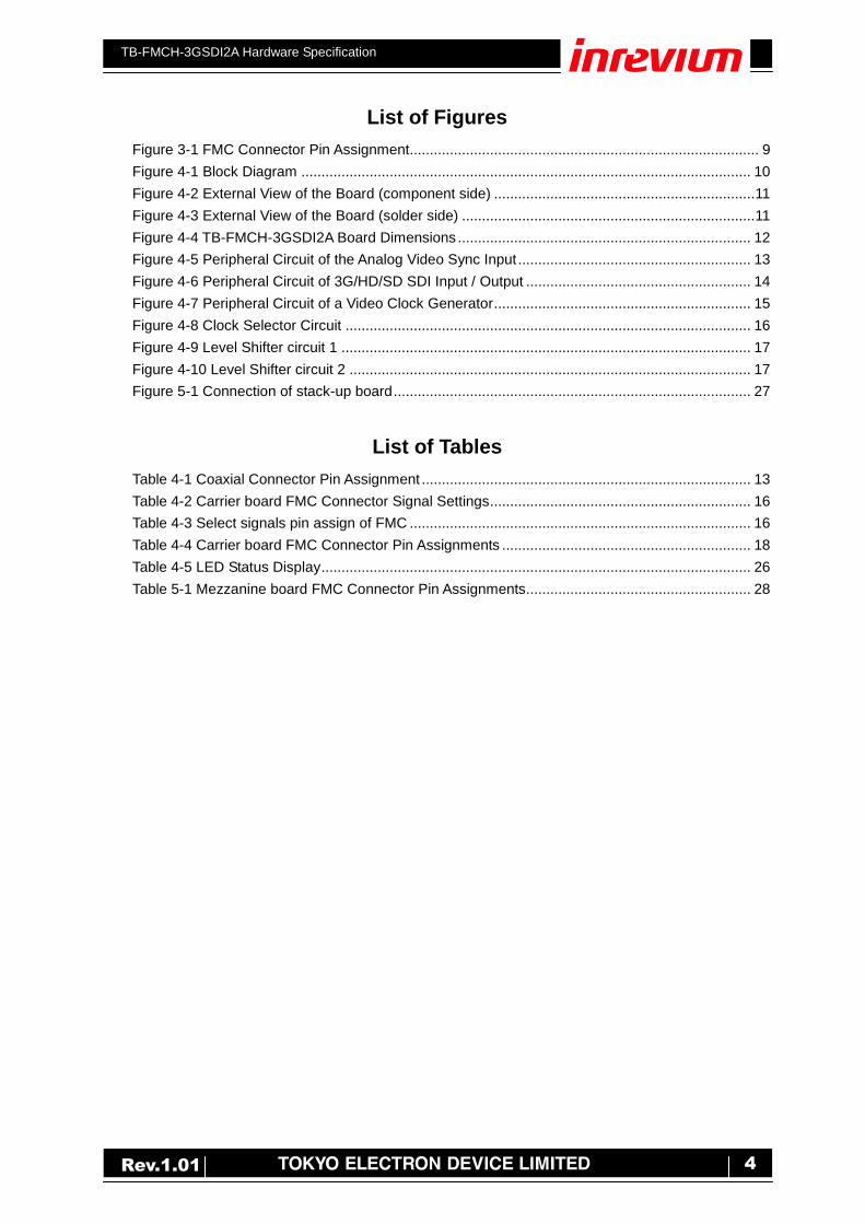
4.8. Clock Selector
This clock selector provide clock from Video Clock Generator(LMH1983), OSC 148.5MHz or OSC 148.3516MHz. Clock select signals(S10,S11,S20,S21) connect to FMC connector. The following figure shows the clock selector circuit.
Figure 4-8 Clock Selector Circuit
Table 4-2 Clock Select Settings
S10 S11 CLKout2 output to Carrier board
Low Low Onboard CLKout2
Low High Onboard CLKout3
High Low OSC 148.5MHz
High High OSC 148.3516MHz
S20 S21 CLKout3 output to Carrier board
Low Low Onboard CLKout2
Low High Onboard CLKout3
High Low OSC 148.5MHz
High High OSC 148.3516MHz
Table 4-3 Select signals pin assign of FMC
Signals Pin
S10 LA11_P
S11 LA11_N
S20 LA15_P
S21 LA15_N

TB-FMCH-3GSDI2A Hardware Specification
17 Rev.1.01
4.9. IO voltage
All of standard IO signals through Level Shifter. Signal level is converting to voltage of VADJ. Please check the VADJ of carrier board before design FPGA.
Figure 4-9 Level Shifter circuit 1
Figure 4-10 Level Shifter circuit 2
TB-FMCH-3GSDI2A Hardware Specification
18 Rev.1.01
4.10. FMC Connector to Carrier board
The board uses Samtec ASP-134488-01 (High-Pin Count) on the solder side of the board for mounting onto the Carrier board.
Table 4-4 FMC Connector Pin Assignments to Carrier board
A-column (FMC Connector for Carrier board)
No. FMC Spec I/O Signal Name Description
1 GND - - -
2 DP1_M2C_P O CH1_SDO_p SDI signal output from LMH0387 on CH1 (positive) 3 DP1_M2C_N O CH1_SDO_n SDI signal output from LMH0387 on CH1 (negative) 4 GND - - -
5 GND - - -
6 DP2_M2C_P O CH2_SDO_p SDI signal output from LMH0387 on CH2 (positive) 7 DP2_M2C_N O CH2_SDO_n SDI signal output from LMH0387 on CH2 (negative) 8 GND - - -
9 GND - - -
10 DP3_M2C_P O CH3_SDO_p SDI signal output from LMH0387 on CH3 (positive) 11 DP3_M2C_N O CH3_SDO_n SDI signal output from LMH0387 on CH3 (negative) 12 GND - - -
13 GND - - -
14 DP4_M2C_P O EX_CH0_SDO_p CH0-RX of Stacked Board(POS)
15 DP4_M2C_N O EX_CH0_SDO_n CH0-RX of Stacked Board(NEG)
16 GND - - -
17 GND - - -
18 DP5_M2C_P O EX_CH1_SDO_p CH1-RX of Stacked Board(POS)
19 DP5_M2C_N O EX_CH1_SDO_n CH1-RX of Stacked Board(NEG)
20 GND - - -
21 GND - - -
22 DP1_C2M_P I CH1_SDI_p SDI signal input to LMH0387 on CH1 (positive) 23 DP1_C2M_N I CH1_SDI_n SDI signal input to LMH0387 on CH1 (negative) 24 GND - - -
25 GND - - -
26 DP2_C2M_P I CH2_SDI_p SDI signal input to LMH0387 on CH2 (positive) 27 DP2_C2M_N I CH2_SDI_n SDI signal input to LMH0387 on CH2 (negative) 28 GND - - -
29 GND - - -
30 DP3_C2M_P I CH3_SDI_p SDI signal input to LMH0387 on CH3 (positive) 31 DP3_C2M_N I CH3_SDI_n SDI signal input to LMH0387 on CH3 (negative) 32 GND - - -
33 GND - - -
34 DP4_C2M_P I EX_CH0_SDI_p CH0-TX of Stacked Board(POS)
35 DP4_C2M_N I EX_CH0_SDI_n CH0-TX of Stacked Board(NEG)
36 GND - - -
37 GND - - -
38 DP5_C2M_P I EX_CH1_SDI_p CH1-TX of Stacked Board(POS)
39 DP5_C2M_N I EX_CH1_SDI_n CH1-TX of Stacked Board(NEG)
40 GND - - -

TB-FMCH-3GSDI2A Hardware Specification
19 Rev.1.01
B-column (FMC Connector for Carrier board)
No. FMC Spec I/O Signal Name Description
1 RES1 - N/C -
2 GND - - -
3 GND - - -
4 DP9_M2C_P - N/C -
5 DP9_M2C_N - N/C -
6 GND - - -
7 GND - - -
8 DP8_M2C_P - N/C -
9 DP8_M2C_N - N/C -
10 GND - - -
11 GND - - -
12 DP7_M2C_P O EX_CH3_SDO_p CH3-RX of Stacked Board(POS)
13 DP7_M2C_N O EX_CH3_SDO_n CH3-RX of Stacked Board(NEG)
14 GND - - -
15 GND - - -
16 DP6_M2C_P O EX_CH2_SDO_p CH2-RX of Stacked Board(POS)
17 DP6_M2C_N O EX_CH2_SDO_n CH2-RX of Stacked Board(NEG)
18 GND - - -
19 GND - - -
20 GBTCLK1_M2C_P O F_CLKout3_p CLKout3 output from selected LMH1983
(positive)
21 GBTCLK1_M2C_N O F_CLKout3_n CLKout3 output from selected LMH1983
(negative)
22 GND - - -
23 GND - - -
24 DP9_C2M_P - N/C -
25 DP9_C2M_N - N/C -
26 GND - - -
27 GND - - -
28 DP8_C2M_P - N/C -
29 DP8_C2M_N - N/C -
30 GND - - -
31 GND - - -
32 DP7_C2M_P I EX_CH3_SDI_p CH3-TX of Stacked Board(POS)
33 DP7_C2M_N I EX_CH3_SDI_n CH3-TX of Stacked Board(NEG)
34 GND - - -
35 GND - - -
36 DP6_C2M_P I EX_CH2_SDI_p CH2-TX of Stacked Board(POS)
37 DP6_C2M_N I EX_CH2_SDI_n CH2-TX of Stacked Board(NEG)
38 GND - - -
39 GND - - -
40 RES0 - N/C -

TB-FMCH-3GSDI2A Hardware Specification
20 Rev.1.01
C-column (FMC Connector for Carrier board)
No. FMC Spec I/O Signal Name Description
1 GND - - -
2 DP0_C2M_P I CH0_SDI_p SDI signal input to LMH0387 on EXP CH0
(positive)
3 DP0_C2M_N I CH0_SDI_n SDI signal input to LMH0387 on EXP CH0
(negative)
4 GND - - -
5 GND - - -
6 DP0_M2C_P O CH0_SDO_p SDI signal output from LMH0387 on CH0
(positive)
7 DP0_M2C_N O CH0_SDO_n SDI signal output from LMH0387 on CH0
(positive)
8 GND - - -
9 GND - - -
10 LA06_P I F_CH0T_SD SD/HD pin input to LMH0387 on CH0 TX
11 LA06_N I F_CH0R_SD SD/HD pin input to LMH0387 on CH0 RX
12 GND - -
13 GND - - -
14 LA10_P I F_CH1T_SD SD/HD pin input to LMH0387 on CH1 TX
15 LA10_N I F_CH1R_SD SD/HD pin input to LMH0387 on CH1 RX
16 GND - - -
17 GND - - -
18 LA14_P I F_CH2_SD SD/HD pin input to LMH0387 on CH2
19 LA14_N I F_CH3_SD SD/HD pin input to LMH0387 on CH3
20 GND - - -
21 GND - - -
22 LA18_P_CC I F_CH2_TXEN TX_EN pin input to LMH0387 on CH2
23 LA18_N_CC I F_CH3_TXEN TX_EN pin input to LMH0387 on CH3
24 GND - - -
25 GND - - -
26 LA27_P I EX_SCL_1983 SCL of stacked LMH1983
27 LA27_N I/O EX_SDA_1983 SDA of stacked LMH1983
28 GND - - -
29 GND - - -
30 SCL I SCL M24C02-WDW6(U21) SCL pin
31 SDA I/O SDA M24C02-WDW6(U21) SDA pin
32 GND - - -
33 GND - - -
34 GA0 I E0 of U21 M24C02-WDW6(U21) E0 pin
35 12P0V - +12V +12V power supply
36 GND - - -
37 12P0V - +12V +12V power supply
38 GND - - -
39 3P3V - +3.3V +3.3V power supply
40 GND - - -
TB-FMCH-3GSDI2A Hardware Specification
21 Rev.1.01
D-column (FMC Connector for Carrier board)
No. FMC Spec I/O Signal Name Description
1 PG_C2M - N/C -
2 GND - - -
3 GND - - -
4 GBTCLK0_M2C_P O F_CLKout2_p CLKout2 output from selected LMH1983
(positive)
5 GBTCLK0_M2C_N O F_CLKout2_n CLKout2 output from selected LMH1983
(negative)
6 GND - - -
7 GND - - -
8 LA01_P_CC I F_CH0T_SEL SS pin input to LMH0387 on CH0 TX
9 LA01_N_CC I F_CH0R_SEL SS pin input to LMH0387 on CH0 RX
10 GND - - -
11 LA05_P I F_CH1T_SEL SS pin input to LMH0387 on CH1 TX
12 LA05_N I F_CH1R_SEL SS pin input to LMH0387 on CH1 RX
13 GND - - -
14 LA09_P I F_CH2_SEL SS pin input to LMH0387 on CH2
15 LA09_N I F_CH3_SEL SS pin input to LMH0387 on CH3
16 GND - - -
17 LA13_P I F_MOSI MOSI pin input to LMH0387 on all CHs
18 LA13_N O F_MISO MISO pin output from LMH0387 on all CHs
19 GND - - -
20 LA17_P_CC I F_SCLK SCK pin input to LMH0387 on all CHs
21 LA17_N_CC - N/C -
22 GND - - -
23 LA23_P I EX_S10 Clock Select signal of stacked board
24 LA23_N I EX_S11 Clock Select signal of stacked board
25 GND - - -
26 LA26_P I EX_S20 Clock Select signal of stacked board
27 LA26_N I EX_S21 Clock Select signal of stacked board
28 GND - - -
29 TCK - N/C -
30 TDI - N/C -
31 TDO - N/C -
32 3P3VAUX - +3.3V_AUX +3.3V_AUX power supply
33 TMS - N/C -
34 TRST_L - N/C -
35 GA1 I E1 of U21 M24C02-WDW6(U21) E1 pin
36 3P3V - +3.3V +3.3V power supply
37 GND - - -
38 3P3V - +3.3V +3.3V power supply
39 GND - - -
40 3P3V - +3.3V +3.3V power supply
TB-FMCH-3GSDI2A Hardware Specification
22 Rev.1.01
E-column (FMC Connector for Carrier board)
F-column (FMC Connector for Carrier board)
No. FMC Spec I/O Signal Name
Description
No. FMC Spec I/O Signal Name
Description
1 GND - - -
1 PG_M2C - Test Pad TP5
2 HA01_P_CC - N/C -
2 GND - - -
3 HA01_N_CC - N/C -
3 GND - - -
4 GND - - -
4 HA00_P_CC - N/C -
5 GND - - -
5 HA00_N_CC - N/C -
6 HA05_P - N/C -
6 GND - - -
7 HA05_N - N/C -
7 HA04_P - N/C -
8 GND - - -
8 HA04_N - N/C -
9 HA09_P - N/C -
9 GND - - -
10 HA09_N - N/C -
10 HA08_P - N/C -
11 GND - - -
11 HA08_N - N/C -
12 HA13_P - N/C -
12 GND - - -
13 HA13_N - N/C -
13 HA12_P - N/C -
14 GND - - -
14 HA12_N - N/C -
15 HA16_P - N/C -
15 GND - - -
16 HA16_N - N/C -
16 HA15_P - N/C -
17 GND - - -
17 HA15_N - N/C -
18 HA20_P - N/C -
18 GND - - -
19 HA20_N - N/C -
19 HA19_P - N/C -
20 GND - - -
20 HA19_N - N/C -
21 HB03_P - N/C -
21 GND - - -
22 HB03_N - N/C -
22 HB02_P - N/C -
23 GND - - -
23 HB02_N - N/C -
24 HB05_P - N/C -
24 GND - - -
25 HB05_N - N/C -
25 HB04_P - N/C -
26 GND - - -
26 HB04_N - N/C -
27 HB09_P - N/C -
27 GND - - -
28 HB09_N - N/C -
28 HB08_P - N/C -
29 GND - - -
29 HB08_N - N/C -
30 HB13_P - N/C -
30 GND - - -
31 HB13_N - N/C -
31 HB12_P - N/C -
32 GND - - -
32 HB12_N - N/C -
33 HB19_P - N/C -
33 GND - - -
34 HB19_N - N/C -
34 HB16_P - N/C -
35 GND - - -
35 HB16_N - N/C -
36 HB21_P - N/C -
36 GND - - -
37 HB21_N - N/C -
37 HB20_P - N/C -
38 GND - - -
38 HB20_N - N/C -
39 VADJ - FMC_VADJ VADJ power supply
39 GND - - -
40 GND - - -
40 VADJ - FMC_VADJ VADJ power supply

TB-FMCH-3GSDI2A Hardware Specification
23 Rev.1.01
G-column (FMC Connector for Carrier board)
No. FMC Spec I/O Signal Name Description
1 GND - - -
2 CLK0_M2C_P O CLKout4_p CLKout4 output from LMH1983 (positive) 3 CLK0_M2C_N O CLKout4_n CLKout4 output from LMH1983 (negative) 4 GND - - -
5 GND - - -
6 LA00_P_CC O F_Fout2 Fout2 output from LMH1983
7 LA00_N_CC O F_Fout3 Fout3 output from LMH1983
8 GND - - -
9 LA03_P O F_Fout1 Fout1 output from LMH1983
10 LA03_N O F_Fout4 Fout4 output from LMH1983
11 GND - - -
12 LA08_P O F_Vout Vout ouput from LMH1981
13 LA08_N O F_Hout Hout output from LMH1981
14 GND - - -
15 LA12_P O F_Fout Fout output from LMH1981
16 LA12_N I F_INIT INIT pin input to LMH1983
17 GND - - -
18 LA16_P I F_Vin Vin pin input to LMH1983
19 LA16_N I F_Hin Hin pin input to LMH1983
20 GND - - -
21 LA20_P I F_Fin Fin input to LMH1983
22 LA20_N - - -
23 GND - - -
24 LA22_P I EX_CH0T_SD SD/HD pin of stacked CH0 TX
25 LA22_N I EX_CH0R_SD SD/HD pin of stacked CH0 RX
26 GND - - -
27 LA25_P I EX_CH1T_SD SD/HD pin of stacked CH1 TX
28 LA25_N I EX_CH1R_SD SD/HD pin of stacked CH1 RX
29 GND - - -
30 LA29_P I EX_CH2_SD SD/HD pin of stacked CH2
31 LA29_N I EX_CH3_SD SD/HD pin of stacked CH3
32 GND - - -
33 LA31_P I EX_CH2_TXEN TXEN pin of stacked CH2
34 LA31_N I EX_CH3_TXEN TXEN pin of stacked CH3
35 GND - - -
36 LA33_P - N/C -
37 LA33_N - N/C -
38 GND - - -
39 VADJ - FMC_VADJ VADJ power supply
40 GND - - -

TB-FMCH-3GSDI2A Hardware Specification
24 Rev.1.01
H-column (FMC Connector for Carrier board)
No. FMC Spec I/O Signal Name Description
1 VREF_A_M2C - Test Pad -
2 PRSNT_M2C_L - N/C -
3 GND - - -
4 CLK0_M2C_P O CLKout1_p CLKout1 output from LMH1983
(positive)
5 CLK0_M2C_N O CLKout1_n CLKout1 output from LMH1983
(negative)
6 GND - - -
7 LA02_P O F_NO_REF NO_REF pin output from LMH1983
8 LA02_N O F_NO_ALIGN NO_ALIGN pin output from
LMH1983
9 GND - - -
10 LA04_P O F_NO_LOCK NO_LOCK pin output from LMH1983
11 LA04_N - N/C -
12 GND - - -
13 LA07_P I F_CL_1983 SCL pin input to LMH1983
14 LA07_N I/O F_DA_1983 SDA pin input/output to/from
LMH1983
15 GND - - -
16 LA11_P I F_S10 Clock Select Signal S10
17 LA11_N I F_S11 Clock Select Signal S11
18 GND - - -
19 LA15_P I F_S20 Clock Select Signal S20
20 LA15_N I F_S21 Clock Select Signal S21
21 GND - - -
22 LA19_P I EX_CH0T_SEL SS pin of stacked CH0 TX
23 LA19_N I EX_CH0R_SEL SS pin of stacked CH0 RX
24 GND - - -
25 LA21_P I EX_CH1T_SEL SS pin of stacked CH1 TX
26 LA21_N I EX_CH1R_SEL SS pin of stacked CH1 RX
27 GND - - -
28 LA24_P I EX_CH2_SEL SS pin of stacked CH2
29 LA24_N I EX_CH3_SEL SS pin of stacked CH3
30 GND - - -
31 LA28_P I EX_MOSI MOSI pin of stacked board
32 LA28_N I/O EX_MISO MISO pin of stacked board
33 GND - - -
34 LA30_P I EX_SCLK SCLK pin of stacked board
35 LA30_N - N/C -
36 GND - - -
37 LA32_P - N/C -
38 LA32_N - N/C -
39 GND - - -
40 VADJ - FMC_VADJ VADJ power supply

TB-FMCH-3GSDI2A Hardware Specification
25 Rev.1.01
J-column (FMC Connector for Carrier board)
K-column (FMC Connector for Carrier board)
No. FMC Spec I/O Signal Name
Description
No. FMC Spec I/O Signal Name
Description
1 GND - - -
1 VREF_B_M2C - Test Pad
TP3
2 CLK3_M2C_P - N/C -
2 GND - - -
3 CLK3_M2C_N - N/C -
3 GND - - -
4 GND - - -
4 CLK2_M2C_P - N/C -
5 GND - - -
5 CLK2_M2C_N - N/C -
6 HA03_P - N/C -
6 GND - - -
7 HA03_N - N/C -
7 HA02_P - N/C -
8 GND - - -
8 HA02_N - N/C -
9 HA07_P - N/C -
9 GND - - -
10 HA07_N - N/C -
10 HA06_P - N/C -
11 GND - - -
11 HA06_N - N/C -
12 HA11_P - N/C -
12 GND - - -
13 HA11_N - N/C -
13 HA10_P - N/C -
14 GND - - -
14 HA10_N - N/C -
15 HA14_P - N/C -
15 GND - - -
16 HA14_N - N/C -
16 HA17_P_CC - N/C -
17 GND - - -
17 HA17_N_CC - N/C -
18 HA18_P - N/C -
18 GND - - -
19 HA18_N - N/C -
19 HA21_P - N/C -
20 GND - - -
20 HA21_N - N/C -
21 HA22_P - N/C -
21 GND - - -
22 HA22_N - N/C -
22 HA23_P - N/C -
23 GND - - -
23 HA23_N - N/C -
24 HB01_P - N/C -
24 GND - - -
25 HB01_N - N/C -
25 HB00_P_CC - N/C -
26 GND - - -
26 HB00_N_CC - N/C -
27 HB07_P - N/C -
27 GND - - -
28 HB07_N - N/C -
28 HB06_P_CC - N/C -
29 GND - - -
29 HB06_N_CC - N/C -
30 HB11_P - N/C -
30 GND - - -
31 HB11_N - N/C -
31 HB10_P - N/C -
32 GND - - -
32 HB10_N - N/C -
33 HB15_P - N/C -
33 GND - - -
34 HB15_N - N/C -
34 HB14_P - N/C -
35 GND - - -
35 HB14_N - N/C -
36 HB18_P - N/C -
36 GND - - -
37 HB18_N - N/C -
37 HB17_P_CC - N/C -
38 GND - - -
38 HB17_N_CC - N/C -
39 VIO_B_M2C - Test Pad
TP6
39 GND - - -
40 GND - - -
40 VIO_B_M2C - Test Pad
TP7

TB-FMCH-3GSDI2A Hardware Specification
26 Rev.1.01
4.11. FMC Connector to Stack-up 3GSDI2 board
The board uses Samtec ASP-134486-01(High-Pin Count) on the component side of the board for mounting onto the Carrier board. Please refer to Section 5 Stack-up configuration. 4.12. LED Display
Table 4-5 shows the status information provided by onboard LEDs.
Table 4-5 LED Status Display
No Circuit# Description Status
1 D2 LMH0387 carrier detection on CH0 RX OFF: Detect, ON: Non-detect
2 D4 LMH0387 carrier detection on CH1 RX OFF: Detect, ON: Non-detect
3 D8 LMH0387 carrier detection on CH2 OFF: Detect, ON: Non-detect
4 D9 LMH0387 carrier detection on CH3 OFF: Detect, ON: Non-detect
5 D5 LMH1983 NO_LOCK pin OFF: Detect, ON: Non-detect
6 D6 LMH1983 NO_ALIGN pin OFF: Detect, ON: Non-detect
7 D7 LMH1983 NO_REF pin OFF: Detect, ON: Non-detect
TB-FMCH-3GSDI2A Hardware Specification
27 Rev.1.01
5. Stack-up configuration TB-FMCH-3GSDI2A support stack-up configuration. In this case, SDI channel is 4ch input, 4ch output and 4ch bi-directional. At same time, Genlock circuit of stacked board is disabled.
LA Group
LA Group
LA Group
LA Group
LA Group
LA Group
LA Group LA Group
CH0_SDI_p/n
Fout/Vout/Hout
Fin/Vin/Hin
INIT
CLKout1_p/n
CLKout2_p/n
CLKout4_p/n
NO_REF/NO_ALIGN/NO_LOCK
CLKout3_p/n
SCL_1983/SDA_1983
CH0_SDO_p/n
CH0R_SD/SEL
CH2_SDI_p/n
CH2_SDO_p/n
CH2_TXEN/SD/SEL
CH1_SDI_p/n
CH1_SDO_p/n
CH0R_SD/SEL
CH3_SDI_p/n
CH3_SDO_p/n
CH3_TXEN/SD/SEL
Clo
ck
Se
lecto
r
EX_CH0_SDI_p/n
EX_CH0_SDO_p/n
EX_CH4R_SD/SEL
EX_CH2_SDI_p/n
EX_CH2_SDO_p/n
EX_CH2_TXEN/SD/SEL
EX_CH1_SDI_p/n
EX_CH1_SDO_p/n
EX_CH1R_SD/SEL
EX_CH3_SDI_p/n
EX_CH3_SDO_p/n
EX_CH3_TXEN/SD/SEL
S10,S11
S20,S21
148.5M
148.3516M
Fin/Vin/Hin
INIT
CLKout1_p/n
CLKout4_p/n
NO_REF/NO_ALIGN/NO_LOCK
EX_SCL_1983/EX_SDA_1983
Fout/Vout/Hout
FMC-HPC
(for stacked board)
ASP-134486-01
FMC-HPC
(for Carrier Board)
ASP-134488-01
DP
0D
P1
DP
2D
P3
DP
4D
P5
DP
6D
P7
DP
0D
P1
DP
2D
P3
EX_S10, EX_S11
EX_S20, EX_S21
TP
TP
TP
TP
TP
TP
MOSI/MISO/SCLKEX_MOSI/EX_MISO/EX_SCLK
Figure 5-1 Connection of stack-up board

TB-FMCH-3GSDI2A Hardware Specification
28 Rev.1.01
Table 5-1 FMC Connector Pin Assignments for Mezzanine board
A-column (FMC Connector for Mezzanine board)
No. FMC Spec I/O Signal Name Description
1 GND - - -
2 DP1_M2C_P I EX_CH1_SDO_p CH1-RX of Stacked Board(POS)
3 DP1_M2C_N I EX_CH1_SDO_n CH1-RX of Stacked Board(NEG)
4 GND - - -
5 GND - - -
6 DP2_M2C_P I EX_CH2_SDO_p CH2-RX of Stacked Board(POS)
7 DP2_M2C_N I EX_CH2_SDO_n CH2-RX of Stacked Board(NEG)
8 GND - - -
9 GND - - -
10 DP3_M2C_P I EX_CH3_SDO_p CH3-RX of Stacked Board(POS)
11 DP3_M2C_N I EX_CH3_SDO_n CH3-RX of Stacked Board(NEG)
12 GND - - -
13 GND - - -
14 DP4_M2C_P - N/C -
15 DP4_M2C_N - N/C -
16 GND - - -
17 GND - - -
18 DP5_M2C_P - N/C -
19 DP5_M2C_N - N/C -
20 GND - - -
21 GND - - -
22 DP1_C2M_P O EX_CH1_SDI_p CH1-TX of Stacked Board(POS)
23 DP1_C2M_N O EX_CH1_SDI_n CH1-TX of Stacked Board(NEG)
24 GND - - -
25 GND - - -
26 DP2_C2M_P O EX_CH2_SDI_p CH2-TX of Stacked Board(POS)
27 DP2_C2M_N O EX_CH2_SDI_n CH2-TX of Stacked Board(NEG)
28 GND - - -
29 GND - - -
30 DP3_C2M_P O EX_CH3_SDI_p CH3-TX of Stacked Board(POS)
31 DP3_C2M_N O EX_CH3_SDI_n CH3-TX of Stacked Board(NEG)
32 GND - - -
33 GND - - -
34 DP4_C2M_P - N/C -
35 DP4_C2M_N - N/C -
36 GND - - -
37 GND - - -
38 DP5_C2M_P - N/C -
39 DP5_C2M_N - N/C -
40 GND - - -
TB-FMCH-3GSDI2A Hardware Specification
29 Rev.1.01
B-column (FMC Connector for Mezzanine board)
No. FMC Spec I/O Signal Name Description
1 RES1 - N/C -
2 GND - - -
3 GND - - -
4 DP9_M2C_P - N/C -
5 DP9_M2C_N - N/C -
6 GND - - -
7 GND - - -
8 DP8_M2C_P - N/C -
9 DP8_M2C_N - N/C -
10 GND - - -
11 GND - - -
12 DP7_M2C_P - N/C -
13 DP7_M2C_N - N/C -
14 GND - - -
15 GND - - -
16 DP6_M2C_P - N/C -
17 DP6_M2C_N - N/C -
18 GND - - -
19 GND - - -
20 GBTCLK1_M2C_P - N/C -
21 GBTCLK1_M2C_N - N/C -
22 GND - - -
23 GND - - -
24 DP9_C2M_P - N/C -
25 DP9_C2M_N - N/C -
26 GND - - -
27 GND - - -
28 DP8_C2M_P - N/C -
29 DP8_C2M_N - N/C -
30 GND - - -
31 GND - - -
32 DP7_C2M_P - N/C -
33 DP7_C2M_N - N/C -
34 GND - - -
35 GND - - -
36 DP6_C2M_P - N/C -
37 DP6_C2M_N - N/C -
38 GND - - -
39 GND - - -
40 RES0 - N/C -
TB-FMCH-3GSDI2A Hardware Specification
30 Rev.1.01
C-column (FMC Connector for Mezzanine board)
No. FMC Spec I/O Signal Name Description
1 GND - - -
2 DP0_C2M_P O EX_CH0_SDI_p CH0-TX of Stacked Board(POS)
3 DP0_C2M_N O EX_CH0_SDI_n CH0-TX of Stacked Board(NEG)
4 GND - - -
5 GND - - -
6 DP0_M2C_P I EX_CH0_SDO_p CH0-RX of Stacked Board(POS)
7 DP0_M2C_N I EX_CH0_SDO_n CH0-RX of Stacked Board(NEG)
8 GND - - -
9 GND - - -
10 LA06_P O EX_CH0T_SD SD/HD pin of stacked CH0 TX
11 LA06_N O EX_CH0R_SD SD/HD pin of stacked CH0 RX
12 GND - - -
13 GND - - -
14 LA10_P O EX_CH1T_SD SD/HD pin of stacked CH1 TX
15 LA10_N O EX_CH1R_SD SD/HD pin of stacked CH1 RX
16 GND - - -
17 GND - - -
18 LA14_P O EX_CH2_SD SD/HD pin of stacked CH2
19 LA14_N O EX_CH3_SD SD/HD pin of stacked CH3
20 GND - - -
21 GND - - -
22 LA18_P_CC O EX_CH2_TXEN TXEN pin of stacked CH2
23 LA18_N_CC O EX_CH3_TXEN TXEN pin of stacked CH3
24 GND - - -
25 GND - - -
26 LA27_P - N/C -
27 LA27_N - N/C -
28 GND - - -
29 GND - - -
30 SCL - N/C -
31 SDA - N/C -
32 GND - - -
33 GND - - -
34 GA0 - N/C Connect to Test pad
35 12P0V - +12V +12V power supply
36 GND - - -
37 12P0V - +12V +12V power supply
38 GND - - -
39 3P3V - +3.3V +3.3V power supply
40 GND - - -

TB-FMCH-3GSDI2A Hardware Specification
31 Rev.1.01
D-column (FMC Connector for Mezzanine board)
No. FMC Spec I/O Signal Name Description
1 PG_C2M - N/C -
2 GND - - -
3 GND - - -
4 GBTCLK0_M2C_P - N/C -
5 GBTCLK0_M2C_N - N/C -
6 GND - - -
7 GND - - -
8 LA01_P_CC O EX_CH0T_SEL SS pin of stacked CH0 TX
9 LA01_N_CC O EX_CH0R_SEL SS pin of stacked CH0 RX
10 GND - - -
11 LA05_P O EX_CH1T_SEL SS pin of stacked CH1 TX
12 LA05_N O EX_CH1R_SEL SS pin of stacked CH1 RX
13 GND - - -
14 LA09_P O EX_CH2_SEL SS pin of stacked CH2
15 LA09_N O EX_CH3_SEL SS pin of stacked CH3
16 GND - - -
17 LA13_P O EX_MOSI MOSI pin of stacked board
18 LA13_N I EX_MISO MISO pin of stacked board
19 GND - - -
20 LA17_P_CC O EX_SCLK SCK pin of stacked board
21 LA17_N_CC - N/C -
22 GND - - -
23 LA23_P - N/C -
24 LA23_N - N/C -
25 GND - - -
26 LA26_P - N/C -
27 LA26_N - N/C -
28 GND - - -
29 TCK - N/C -
30 TDI - N/C -
31 TDO - N/C -
32 3P3VAUX - +3.3V_AUX +3.3V_AUX power supply
33 TMS - N/C -
34 TRST_L - N/C -
35 GA1 - N/C Connect to Test pad
36 3P3V - +3.3V +3.3V power supply
37 GND - - -
38 3P3V - +3.3V +3.3V power supply
39 GND - - -
40 3P3V - +3.3V +3.3V power supply

TB-FMCH-3GSDI2A Hardware Specification
32 Rev.1.01
E-column (FMC Connector for Mezzanine board)
F-column (FMC Connector for Mezzanine board)
No. FMC Spec I/O Signal Name
Description
No. FMC Spec I/O Signal Name
Description
1 GND - - -
1 PG_M2C - Test Pad TP5
2 HA01_P_CC - N/C -
2 GND - - -
3 HA01_N_CC - N/C -
3 GND - - -
4 GND - - -
4 HA00_P_CC - N/C -
5 GND - - -
5 HA00_N_CC - N/C -
6 HA05_P - N/C -
6 GND - - -
7 HA05_N - N/C -
7 HA04_P - N/C -
8 GND - - -
8 HA04_N - N/C -
9 HA09_P - N/C -
9 GND - - -
10 HA09_N - N/C -
10 HA08_P - N/C -
11 GND - - -
11 HA08_N - N/C -
12 HA13_P - N/C -
12 GND - - -
13 HA13_N - N/C -
13 HA12_P - N/C -
14 GND - - -
14 HA12_N - N/C -
15 HA16_P - N/C -
15 GND - - -
16 HA16_N - N/C -
16 HA15_P - N/C -
17 GND - - -
17 HA15_N - N/C -
18 HA20_P - N/C -
18 GND - - -
19 HA20_N - N/C -
19 HA19_P - N/C -
20 GND - - -
20 HA19_N - N/C -
21 HB03_P - N/C -
21 GND - - -
22 HB03_N - N/C -
22 HB02_P - N/C -
23 GND - - -
23 HB02_N - N/C -
24 HB05_P - N/C -
24 GND - - -
25 HB05_N - N/C -
25 HB04_P - N/C -
26 GND - - -
26 HB04_N - N/C -
27 HB09_P - N/C -
27 GND - - -
28 HB09_N - N/C -
28 HB08_P - N/C -
29 GND - - -
29 HB08_N - N/C -
30 HB13_P - N/C -
30 GND - - -
31 HB13_N - N/C -
31 HB12_P - N/C -
32 GND - - -
32 HB12_N - N/C -
33 HB19_P - N/C -
33 GND - - -
34 HB19_N - N/C -
34 HB16_P - N/C -
35 GND - - -
35 HB16_N - N/C -
36 HB21_P - N/C -
36 GND - - -
37 HB21_N - N/C -
37 HB20_P - N/C -
38 GND - - -
38 HB20_N - N/C -
39 VADJ - FMC_VADJ VADJ power supply
39 GND - - -
40 GND - - -
40 VADJ - FMC_VADJ VADJ power supply

TB-FMCH-3GSDI2A Hardware Specification
33 Rev.1.01
G-column (FMC Connector for Mezzanine board)
No. FMC Spec I/O Signal Name Description
1 GND - - -
2 CLK0_M2C_P I EX_CLKout4_p Connect to Test pad
3 CLK0_M2C_N I EX_CLKout4_n Connect to Test pad
4 GND - - -
5 GND - - -
6 LA00_P_CC I EX_F_Fout2 Connect to Test pad
7 LA00_N_CC I EX_F_Fout3 Connect to Test pad
8 GND - - -
9 LA03_P I EX_F_Fout1 Connect to Test pad
10 LA03_N I EX_F_Fout4 Connect to Test pad
11 GND - - -
12 LA08_P I EX_F_Vout Connect to Test pad
13 LA08_N I EX_F_Hout Connect to Test pad
14 GND - - -
15 LA12_P I EX_F_Fout Connect to Test pad
16 LA12_N I EX_F_INIT Connect to Test pad
17 GND - - -
18 LA16_P I EX_F_Vin Connect to Test pad
19 LA16_N I EX_F_Hin Connect to Test pad
20 GND - - -
21 LA20_P I EX_F_Fin Connect to Test pad
22 LA20_N - N/C -
23 GND - - -
24 LA22_P - N/C -
25 LA22_N - N/C -
26 GND - - -
27 LA25_P - N/C -
28 LA25_N - N/C -
29 GND - - -
30 LA29_P - N/C -
31 LA29_N - N/C -
32 GND - - -
33 LA31_P - N/C -
34 LA31_N - N/C -
35 GND - - -
36 LA33_P - N/C -
37 LA33_N - N/C -
38 GND - - -
39 VADJ - FMC_VADJ VADJ power supply
40 GND - - -

TB-FMCH-3GSDI2A Hardware Specification
34 Rev.1.01
H-column (FMC Connector for Mezzanine board)
No. FMC Spec I/O Signal Name Description
1 VREF_A_M2C - Test Pad -
2 PRSNT_M2C_L - N/C -
3 GND - - -
4 CLK0_M2C_P I EX_CLKout1_p Connect to Test pad
5 CLK0_M2C_N I EX_CLKout1_n Connect to Test pad
6 GND - - -
7 LA02_P I EX_NO_REF Connect to Test pad
8 LA02_N I EX_NO_ALIGN Connect to Test pad
9 GND
10 LA04_P I EX_NO_LOCK Connect to Test pad
11 LA04_N - N/C -
12 GND - - -
13 LA07_P O EX_SCL_1983 SCL of stacked LMH1983
14 LA07_N I/O EX_SDA_1983 SDA of stacked LMH1983
15 GND - - -
16 LA11_P O EX_S10 Clock Select signal of stacked board
17 LA11_N O EX_S11 Clock Select signal of stacked board
18 GND - - -
19 LA15_P O EX_S20 Clock Select signal of stacked board
20 LA15_N O EX_S21 Clock Select signal of stacked board
21 GND - - -
22 LA19_P - N/C -
23 LA19_N - N/C -
24 GND - - -
25 LA21_P - N/C -
26 LA21_N - N/C -
27 GND - - -
28 LA24_P - N/C -
29 LA24_N - N/C -
30 GND - - -
31 LA28_P - N/C -
32 LA28_N - N/C -
33 GND - - -
34 LA30_P - N/C -
35 LA30_N - N/C -
36 GND - - -
37 LA32_P - N/C -
38 LA32_N - N/C -
39 GND - - -
40 VADJ - FMC_VADJ VADJ power supply
TB-FMCH-3GSDI2A Hardware Specification
35 Rev.1.01
J-column (FMC Connector for Mezzanine board)
K-column (FMC Connector for Mezzanine board)
No. FMC Spec I/O Signal Name
Description
No. FMC Spec I/O Signal Name
Description
1 GND - - -
1 VREF_B_M2C - Test Pad
TP3
2 CLK3_M2C_P - N/C -
2 GND - - -
3 CLK3_M2C_N - N/C -
3 GND - - -
4 GND - - -
4 CLK2_M2C_P - N/C -
5 GND - - -
5 CLK2_M2C_N - N/C -
6 HA03_P - N/C -
6 GND - - -
7 HA03_N - N/C -
7 HA02_P - N/C -
8 GND - - -
8 HA02_N - N/C -
9 HA07_P - N/C -
9 GND - - -
10 HA07_N - N/C -
10 HA06_P - N/C -
11 GND - - -
11 HA06_N - N/C -
12 HA11_P - N/C -
12 GND - - -
13 HA11_N - N/C -
13 HA10_P - N/C -
14 GND - - -
14 HA10_N - N/C -
15 HA14_P - N/C -
15 GND - - -
16 HA14_N - N/C -
16 HA17_P_CC - N/C -
17 GND - - -
17 HA17_N_CC - N/C -
18 HA18_P - N/C -
18 GND - - -
19 HA18_N - N/C -
19 HA21_P - N/C -
20 GND - - -
20 HA21_N - N/C -
21 HA22_P - N/C -
21 GND - - -
22 HA22_N - N/C -
22 HA23_P - N/C -
23 GND - - -
23 HA23_N - N/C -
24 HB01_P - N/C -
24 GND - - -
25 HB01_N - N/C -
25 HB00_P_CC - N/C -
26 GND - - -
26 HB00_N_CC - N/C -
27 HB07_P - N/C -
27 GND - - -
28 HB07_N - N/C -
28 HB06_P_CC - N/C -
29 GND - - -
29 HB06_N_CC - N/C -
30 HB11_P - N/C -
30 GND - - -
31 HB11_N - N/C -
31 HB10_P - N/C -
32 GND - - -
32 HB10_N - N/C -
33 HB15_P - N/C -
33 GND - - -
34 HB15_N - N/C -
34 HB14_P - N/C -
35 GND - - -
35 HB14_N - N/C -
36 HB18_P - N/C -
36 GND - - -
37 HB18_N - N/C -
37 HB17_P_CC - N/C -
38 GND - - -
38 HB17_N_CC - N/C -
39 VIO_B_M2C - Test Pad
TP6
39 GND - - -
40 GND - - -
40 VIO_B_M2C - Test Pad
TP7

TB-FMCH-3GSDI2A Hardware Specification
36 Rev.1.01
PLD Solution Dept. PLD Division URL: http://solutions.inrevium.com/
E-mail: [email protected] HEAD Quarter: Yokohama East Square, 1-4 Kinko-cho, Kanagawa-ku, Yokohama City,
Kanagawa, Japan 221-0056 TEL: +81-45-443-4016 FAX: +81-45-443-4058


![Welcome [] and Visitor's Guide 6...We welcome you to take a look around at what FMCH has to offer during your stay with us. FMCH Patient & Visitors Guide iv Page 2 Page 3 Fort Madison](https://img.pdfslide.us/doc/110x75/5b18f13e7f8b9a23258c379f/welcome-and-visitors-guide-6we-welcome-you-to-take-a-look-around-at-what.jpg)


![18F]FMCH PET/CT biomarkers and similarity analysis to rene](https://img.pdfslide.us/doc/110x75/623d3660b7458d4b3c40f8e5/18ffmch-petct-biomarkers-and-similarity-analysis-to-rene-.jpg)