Embed Size (px)
Citation preview

SDIN
MCLK
SCLK
LRCLK
SerialAudioPort
ProtectionLogic
Click and PopControl
Digital Audio Processor(DAP)
SDA
SCL
4Order
th
NoiseShaper
andPWM
SRC
Sample RateAutodetectand PLL
SerialControl
MicrocontrollerBasedSystemControl
Terminal Control
OUT_A
OUT_B
2 HB´
FET Out
OUT_C
OUT_D
2 HB´
FET Out
B0262-06
Copyright © 2016 Texas Instruments Incorporated
Product
Folder
Sample &Buy
Technical
Documents
Tools &
Software
Support &Community
An IMPORTANT NOTICE at the end of this data sheet addresses availability, warranty, changes, use in safety-critical applications,intellectual property matters and other important disclaimers. PRODUCTION DATA.
TAS5727SLOS670A –NOVEMBER 2010–REVISED MAY 2016
TAS5727 25-W Digital Audio Power Amplifier With EQ and DRC
1
1 Features1• Audio Input and Output
– 25 W Into an 8-Ω Load From a 20-V Supply– Wide PVDD Range, From 8 V to 26 V– Supports BTL Configuration With 4-Ω Load– Efficient Class-D Operation Eliminates Need
for Heatsinks– One Serial Audio Input (Two Audio Channels)– I2C Address Selection Pin (Chip Select)– Single Output Filter PBTL Support– Supports 44.1-kHz to 48-kHz Sample Rate
(LJ/RJ/I2S)• Audio and PWM Processing
– Independent Channel Volume Controls WithGain of 24 dB to Mute With 0.125-dBResolution Steps
– Programmable Two-Band Dynamic-RangeControl
– 18 Programmable Biquads for Speaker EQand Other Audio-Processing Features
– Programmable Coefficients for DRC Filters– DC Blocking Filters
• General Features– I2C Serial Control Interface Operational
Without MCLK– Requires Only 3.3 V and PVDD– No External Oscillator: Internal Oscillator for
Automatic Rate Detection– Surface-Mount, 48-Pin HTQFP Package– Thermal and Short-Circuit Protection– 106-dB SNR, A-Weighted
– AD, BD, and Ternary Modulation– Up to 90% Efficient– PWM Level Meter to Measure the Digital
Power Profile• Benefits
– EQ: Speaker Equalization Improves AudioPerformance
– Two-Band DRC: Dynamic RangeCompression. Can Be Used As Power Limiter.Enables Speaker Protection, Easy Listening,Night-Mode Listening
– Autodetect: Automatically Detects Sample-Rate Changes. No Need for ExternalMicroprocessor Intervention
2 Applications• LCD TV, LED TV, Soundbar
3 DescriptionThe TAS5727 is a 25-W, efficient, digital-audio poweramplifier for driving stereo bridge-tied speakers. Oneserial data input allows processing of up to twodiscrete audio channels and seamless integration tomost digital audio processors and MPEG decoders.The device accepts a wide range of input data anddata rates. A fully programmable data path routesthese channels to the internal speaker drivers.
Device Information(1)
PART NUMBER PACKAGE BODY SIZE (NOM)TAS5727 HTQFP (48) 7.00 mm × 7.00 mm
(1) For all available packages, see the orderable addendum atthe end of the data sheet.
Functional View

2
TAS5727SLOS670A –NOVEMBER 2010–REVISED MAY 2016 www.ti.com
Product Folder Links: TAS5727
Submit Documentation Feedback Copyright © 2010–2016, Texas Instruments Incorporated
Table of Contents1 Features .................................................................. 12 Applications ........................................................... 13 Description ............................................................. 14 Revision History..................................................... 25 Description (continued)......................................... 36 Device Comparison Table ..................................... 37 Pin Configuration and Functions ......................... 48 Specifications......................................................... 6
8.1 Absolute Maximum Ratings ...................................... 68.2 ESD Ratings.............................................................. 68.3 Recommended Operating Conditions....................... 68.4 Thermal Information .................................................. 78.5 DC Electrical Characteristics .................................... 78.6 AC Electrical Characteristics (BTL, PBTL)................ 88.7 PLL Input Parameters and External Filter
Components............................................................... 88.8 Serial Audio Ports Slave Mode ................................. 88.9 I2C Serial Control Port Operation.............................. 98.10 Reset Timing (RESET) ........................................... 98.11 Typical Characteristics .......................................... 11
9 Parameter Measurement Information ................ 1210 Detailed Description ........................................... 13
10.1 Overview ............................................................... 13
10.2 Functional Block Diagrams ................................... 1310.3 Feature Description............................................... 1510.4 Device Functional Modes...................................... 2810.5 Programming ........................................................ 2910.6 Register Maps ...................................................... 31
11 Application and Implementation........................ 5411.1 Application Information.......................................... 5411.2 Typical Applications .............................................. 54
12 Power Supply Recommendations ..................... 5912.1 DVDD and AVDD Supplies ................................... 5912.2 PVDD Power Supply............................................. 59
13 Layout................................................................... 6013.1 Layout Guidelines ................................................. 6013.2 Layout Example .................................................... 60
14 Device and Documentation Support ................. 6114.1 Device Support...................................................... 6114.2 Documentation Support ........................................ 6114.3 Community Resources.......................................... 6114.4 Trademarks ........................................................... 6114.5 Electrostatic Discharge Caution............................ 6114.6 Glossary ................................................................ 61
15 Mechanical, Packaging, and OrderableInformation ........................................................... 61
4 Revision HistoryNOTE: Page numbers for previous revisions may differ from page numbers in the current version.
Changes from Original (November 2010) to Revision A Page
• Added ESD Ratings table, Feature Description section, Device Functional Modes, Application and Implementationsection, Power Supply Recommendations section, Layout section, Device and Documentation Support section, andMechanical, Packaging, and Orderable Information section. ................................................................................................. 1
• Changed Section: Overcurrent (OC) Protection With Current Limiting ................................................................................ 16• Changed Section: Overcurrent (OC) Protection With Current Limiting and Overload Detection ......................................... 16

3
TAS5727www.ti.com SLOS670A –NOVEMBER 2010–REVISED MAY 2016
Product Folder Links: TAS5727
Submit Documentation FeedbackCopyright © 2010–2016, Texas Instruments Incorporated
5 Description (continued)The TAS5727 is a slave-only device receiving all clocks from external sources. The TAS5727 operates with aPWM carrier between a 384-kHz switching rate and a 288-KHz switching rate, depending on the input samplerate. Oversampling combined with a fourth-order noise shaper provides a flat noise floor and excellent dynamicrange from 20 Hz to 20 kHz.
6 Device Comparison Table
TAS5727 TAS5729MD TAS5731M TAS5721Maximum power to single-ended load 18 10Maximum power to bridge tied load 35 20 37 15Maximum power to parallel bridge tied load 70 40 70 30Minimum supported single-ended load 2 4Minimum supported bridge tied load 4 4 4 8Minimum supported parallel bridge tied load 2 4 2 4Closed- or open-loop Open Open Open OpenMaximum speaker outputs (#) 2 2 3 3Headphone channels No Yes No YesArchitecture Class D Class D Class D Class DDynamic range control (DRC) 2-Band AGL 2-Band AGL 2-Band DRC 2-Band DRCBiquads (EQ) 28 28 21 21

ThermalPad
48
PG
ND
_A
B13
AV
DD
1OUT_A 36 OUT_D
47
PG
ND
_A
B14
A_S
EL_
FA
ULT
2PVDD_AB 35 PVDD_CD
46
OU
T_B
15
MC
LK
3PVDD_AB 34 PVDD_CD
45
NC
16
OS
C_R
ES
4BST_A 33 BST_D
44
NC
17
DV
SS
O
5NC 32 GVDD_OUT
43
BS
T_B
18
VR
_D
IG
6SSTIMER 31 VREG
42
BS
T_C
19
PD
N
7NC 30 AGND
41
NC
20
LR
CLK
8PBTL 29 GND
40
NC
21
SC
LK
9AVSS 28 DVSS
39
OU
T_C
22
SD
IN
10PLL_FLTM 27 DVDD
38
PG
ND
_C
D23
SD
A
11PLL_FLTP 26 STEST
37
PG
ND
_C
D24
SC
L
12VR_ANA 25 RESET
4
TAS5727SLOS670A –NOVEMBER 2010–REVISED MAY 2016 www.ti.com
Product Folder Links: TAS5727
Submit Documentation Feedback Copyright © 2010–2016, Texas Instruments Incorporated
(1) TYPE: A = analog; D = 3.3-V digital; P = power/ground/decoupling; I = input; O = output(2) All pullups are weak pullups and all pulldowns are weak pulldowns. The pullups and pulldowns are included to assure proper input logic
levels if the pins are left unconnected (pullups → logic 1 input; pulldowns → logic 0 input).
7 Pin Configuration and Functions
PHP Package48-Pin HTQFP
Top View
Pin FunctionsPIN
TYPE (1) 5-VTOLERANT TERMINATION (2) DESCRIPTION
NAME NO.AGND 30 P Local analog ground for power stage

5
TAS5727www.ti.com SLOS670A –NOVEMBER 2010–REVISED MAY 2016
Product Folder Links: TAS5727
Submit Documentation FeedbackCopyright © 2010–2016, Texas Instruments Incorporated
Pin Functions (continued)PIN
TYPE (1) 5-VTOLERANT TERMINATION (2) DESCRIPTION
NAME NO.
A_SEL_FAULT 14 DIO
This pin is monitored on the rising edge of RESET. A value of 0 (15-kΩ pulldown) sets the I2C device address to 0x54 and a value of 1(15-kΩ pullup) sets it to 0x56. this dual-function pin can beprogrammed to output internal power-stage errors.
AVDD 13 P 3.3-V analog power supplyAVSS 9 P Analog 3.3-V supply groundBST_A 4 P High-side bootstrap supply for half-bridge ABST_B 43 P High-side bootstrap supply for half-bridge BBST_C 42 P High-side bootstrap supply for half-bridge CBST_D 33 P High-side bootstrap supply for half-bridge DDVDD 27 P 3.3-V digital power supplyDVSS 28 P Digital groundDVSSO 17 P Oscillator groundGND 29 P Analog ground for power stageGVDD_OUT 32 P Gate drive internal regulator outputLRCLK 20 DI 5-V Pulldown Input serial audio data left and right clock (sample-rate clock)MCLK 15 DI 5-V Pulldown Master clock input
NC
5, 7,40,41,
44, 45
–
No connect
OSC_RES 16 AO Oscillator trim resistor. Connect an 18.2-kΩ, 1% resistor to DVSSO.OUT_A 1 O Output, half-bridge AOUT_B 46 O Output, half-bridge BOUT_C 39 O Output, half-bridge COUT_D 36 O Output, half-bridge D
PBTL 8 DI Low means BTL mode; high means PBTL mode. Information goesdirectly to power stage.
PDN 19 DI 5-V PullupPower down, active-low. PDN prepares the device for loss of powersupplies by shutting down the noise shaper and initiating the PWMstop sequence.
PGND_AB 47, 48 P Power ground for half-bridges A and BPGND_CD 37, 38 P Power ground for half-bridges C and DPLL_FLTM 10 AO PLL negative loop-filter terminalPLL_FLTP 11 AO PLL positive loop-filter terminalPVDD_AB 2, 3 P Power-supply input for half-bridge output APVDD_CD 34, 35 P Power-supply input for half-bridge output D
RESET 25 DI 5-V Pullup
Reset, active-low. A system reset is generated by applying a logiclow to this pin. RESET is an asynchronous control signal thatrestores the DAP to its default conditions and places the PWM in thehard-mute (high-impedance) state.
SCL 24 DI 5-V I2C serial control clock input
SCLK 21 DI 5-V Pulldown Serial audio-data clock (shift clock). SCLK is the serial-audio-portinput-data bit clock.
SDA 23 DIO 5-V I2C serial control data interface input/output
SDIN 22 DI 5-V Pulldown Serial audio data input. SDIN supports three discrete (stereo) dataformats.
SSTIMER 6 AIControls ramp time of OUT_x to minimize pop. Leave this pinfloating for BD mode. Requires capacitor of 2.2 nF to GND in ADmode. The capacitor determines the ramp time.
STEST 26 DI Factory test pin. Connect directly to DVSS.

6
TAS5727SLOS670A –NOVEMBER 2010–REVISED MAY 2016 www.ti.com
Product Folder Links: TAS5727
Submit Documentation Feedback Copyright © 2010–2016, Texas Instruments Incorporated
Pin Functions (continued)PIN
TYPE (1) 5-VTOLERANT TERMINATION (2) DESCRIPTION
NAME NO.
VR_ANA 12 P Internally regulated 1.8-V analog supply voltage. This pin must notbe used to power external devices.
VR_DIG 18 P Internally regulated 1.8-V digital supply voltage. This pin must not beused to power external devices.
VREG 31 P Digital regulator output. Not to be used for powering externalcircuitry.
(1) Stresses beyond those listed under Absolute Maximum Ratings may cause permanent damage to the device. These are stress ratingsonly and functional operation of the device at these or any other conditions beyond those indicated under Recommended OperatingConditions is not implied. Exposure to absolute-maximum conditions for extended periods may affect device reliability.
(2) 5-V tolerant inputs are PDN, RESET, SCLK, LRCLK, MCLK, SDIN, SDA, and SCL.(3) Maximum pin voltage should not exceed 6 V.(4) DC voltage + peak ac waveform measured at the pin should be below the allowed limit for all conditions.
8 Specifications
8.1 Absolute Maximum Ratingsover operating free-air temperature range (unless otherwise noted) (1)
MIN MAX UNIT
Supplyvoltage
DVDD, AVDD –0.3 3.6 VPVDD_x –0.3 30 V
Input voltage3.3-V digital input –0.5 DVDD + 0.5
V5-V tolerant (2) digital input (except MCLK) –0.5 DVDD + 2.5 (3)
5-V tolerant MCLK input –0.5 AVDD + 2.5 (3)
OUT_x to PGND_x 32 (4) VBST_x to PGND_x 43 (4) VInput clamp current, IIK ±20 mAOutput clamp current, IOK ±20 mAOperating free-air temperature 0 85 °COperating junction temperature 0 150 °CStorage temperature, Tstg –40 125 °C
(1) JEDEC document JEP155 states that 500-V HBM allows safe manufacturing with a standard ESD control process.(2) JEDEC document JEP157 states that 250-V CDM allows safe manufacturing with a standard ESD control process.
8.2 ESD RatingsVALUE UNIT
V(ESD) Electrostatic dischargeHuman-body model (HBM), per ANSI/ESDA/JEDEC JS-001 (1) ±1000
VCharged-device model (CDM), per JEDEC specification JESD22-C101 (2) ±250
(1) Continuous operation above the recommended junction temperature may result in reduced reliability and/or lifetime of the device.
8.3 Recommended Operating ConditionsMIN NOM MAX UNIT
Digital/analog supply voltage DVDD, AVDD 3 3.3 3.6 VHalf-bridge supply voltage PVDD_x 8 26 V
VIH High-level input voltage 5-V tolerant 2 VVIL Low-level input voltage 5-V tolerant 0.8 VTA Operating ambient temperature 0 85 °CTJ
(1) Operating junction temperature 0 125 °CRL (BTL) Load impedance Output filter: L = 15 μH, C = 680 nF 4 8 ΩRL (PBTL) Load impedance Output filter: L = 15 μH, C = 680 nF 2 4 Ω

7
TAS5727www.ti.com SLOS670A –NOVEMBER 2010–REVISED MAY 2016
Product Folder Links: TAS5727
Submit Documentation FeedbackCopyright © 2010–2016, Texas Instruments Incorporated
Recommended Operating Conditions (continued)MIN NOM MAX UNIT
LO (BTL) Output-filter inductance Minimum output inductance under short-circuit condition 10 μH
Output sample rate11.025/22.05/44.1-kHz data rate ±2% 288
kHz48/24/12/8/16/32-kHz data rate ±2% 384
(1) For more information about traditional and new thermal metrics, see the Semiconductor and IC Package Thermal Metrics applicationreport, SPRA953.
8.4 Thermal Information
THERMAL METRIC (1)TAS5727
UNITPHP (HTQFP)48 PINS
RθJA Junction-to-ambient thermal resistance 27.9 °C/WRθJC(top) Junction-to-case (top) thermal resistance 13 °C/WRθJB Junction-to-board thermal resistance 1.1 °C/WψJT Junction-to-top characterization parameter 20.7 °C/WψJB Junction-to-board characterization parameter 0.3 °C/WRθJC(bot) Junction-to-case (bottom) thermal resistance 6.7 °C/W
(1) IIH for the PBTL pin has a maximum limit of 200 µA due to an internal pulldown on the pin.(2) This does not include bond-wire or pin resistance.(3) Specified by design
8.5 DC Electrical CharacteristicsTA = 25°, PVCC_x = 18 V, DVDD = AVDD = 3.3 V, RL= 8 Ω, BTL AD mode, fS = 48 kHz (unless otherwise noted)
PARAMETER TEST CONDITIONS MIN TYP MAX UNIT
VOH High-level output voltage A_SEL_FAULT and SDA IOH = –4 mADVDD = 3 V 2.4 V
VOL Low-level output voltage A_SEL_FAULT and SDA IOL = 4 mADVDD = 3 V 0.5 V
IIL Low-level input current VI < VIL ; DVDD = AVDD= 3.6 V 75 μA
IIH High-level input current VI > VIH ; DVDD =AVDD = 3.6 V 75 (1) μA
IDD 3.3-V supply current 3.3-V supply voltage (DVDD,AVDD)
Normal mode 49 68mAReset (RESET = low,
PDN = high) 23 38
IPVDD Supply current No load (PVDD_x)Normal mode 32 50
mAReset (RESET = low,PDN = high) 3 8
rDS(on)(2) Drain-to-source resistance, LS TJ = 25°C, includes metallization resistance 75
mΩDrain-to-source resistance, HS TJ = 25°C, includes metallization resistance 75
I/O ProtectionVuvp Undervoltage protection limit PVDD falling 7.2 VVuvp,hyst Undervoltage protection limit PVDD rising 7.6 VOTE (3) Overtemperature error 150 °C
OTEHYST(3) Extra temperature drop
required to recover from error 30 °C
IOC Overcurrent limit protection 4.5 AIOCT Overcurrent response time 150 ns
RPDInternal pulldown resistor at theoutput of each half-bridge
Connected when drivers are in the high-impedance stateto provide bootstrap capacitor charge. 3 kΩ

8
TAS5727SLOS670A –NOVEMBER 2010–REVISED MAY 2016 www.ti.com
Product Folder Links: TAS5727
Submit Documentation Feedback Copyright © 2010–2016, Texas Instruments Incorporated
(1) SNR is calculated relative to 0-dBFS input level.
8.6 AC Electrical Characteristics (BTL, PBTL)PVDD_x = 18 V, BTL AD mode, fS = 48 KHz, RL = 8 Ω, ROCP = 22 kΩ, CBST = 33 nF, audio frequency = 1 kHz, AES17 filter,fPWM = 384 kHz, TA = 25°C (unless otherwise specified). All performance is in accordance with recommended operatingconditions (unless otherwise specified).
PARAMETER TEST CONDITIONS MIN TYP MAX UNIT
PO Power output per channel
PVDD = 18 V,10% THD, 1-kHz input signal 21.5
W
PVDD = 18 V, 7% THD, 1-kHz input signal 20.3PVDD = 12 V, 10% THD, 1-kHz input signal 9.6PVDD = 12 V, 7% THD, 1-kHz input signal 9.1PVDD = 8 V, 10% THD, 1-kHz input signal 4.2PVDD = 8 V, 7% THD, 1-kHz input signal 4PBTL mode, PVDD = 12 V, RL = 4 Ω,10% THD, 1-kHz input signal 18.7
PBTL mode, PVDD = 12 V, RL = 4 Ω,7% THD, 1-kHz input signal 17.7
PBTL mode, PVDD = 18 V, RL = 4 Ω,10% THD, 1-kHz input signal 41.5
PBTL mode, PVDD = 18 V, RL = 4 Ω,7% THD, 1-kHz input signal 39
THD+N Total harmonic distortion + noisePVDD = 18 V, PO = 1 W 0.07%PVDD = 12 V, PO = 1 W 0.03%PVDD = 8 V, PO = 1 W 0.1%
Vn Output integrated noise (rms) A-weighted 56 μV
CrosstalkPO = 0.25 W, f = 1 kHz (BD Mode) –82 dBPO = 0.25 W, f = 1 kHz (AD Mode) –69 dB
SNR Signal-to-noise ratio (1) A-weighted, f = 1 kHz, maximum power atTHD < 1% 106 dB
8.7 PLL Input Parameters and External Filter ComponentsPARAMETER TEST CONDITIONS MIN TYP MAX UNIT
fMCLKI MCLK frequency 2.8224 24.576 MHzMCLK duty cycle 40% 50% 60%
tr /tf(MCLK)
Rise/fall time for MCLK 5 ns
LRCLK allowable drift before LRCLK reset 4 MCLKsExternal PLL filter capacitor C1 SMD 0603 X7R 47 nFExternal PLL filter capacitor C2 SMD 0603 X7R 4.7 nFExternal PLL filter resistor R SMD 0603, metal film 470 Ω
8.8 Serial Audio Ports Slave Modeover recommended operating conditions (unless otherwise noted)
PARAMETER TEST CONDITIONS MIN NOM MAX UNITfSCLKIN Frequency, SCLK 32 × fS, 48 × fS, 64 × fS CL = 30 pF 1.024 12.288 MHztsu1 Setup time, LRCLK to SCLK rising edge 10 nsth1 Hold time, LRCLK from SCLK rising edge 10 nstsu2 Setup time, SDIN to SCLK rising edge 10 nsth2 Hold time, SDIN from SCLK rising edge 10 ns
LRCLK frequency 8 48 48 kHzSCLK duty cycle 40% 50% 60%LRCLK duty cycle 40% 50% 60%

th1
tsu1
t(edge)
tsu2
th2
SCLK(Input)
LRCLK(Input)
SDIN
T0026-04
tr tf
9
TAS5727www.ti.com SLOS670A –NOVEMBER 2010–REVISED MAY 2016
Product Folder Links: TAS5727
Submit Documentation FeedbackCopyright © 2010–2016, Texas Instruments Incorporated
Serial Audio Ports Slave Mode (continued)over recommended operating conditions (unless otherwise noted)
PARAMETER TEST CONDITIONS MIN NOM MAX UNIT
SCLK rising edges between LRCLK rising edges 32 64 SCLKedges
t(edge) LRCLK clock edge with respect to the fallingedge of SCLK –1/4 1/4 SCLK
periodtr/tf Rise/fall time for SCLK/LRCLK 8 ns
8.9 I2C Serial Control Port OperationTiming characteristics for I2C Interface signals over recommended operating conditions (unless otherwise noted)
PARAMETER TEST CONDITIONS MIN MAX UNITfSCL Frequency, SCL No wait states 400 kHztw(H) Pulse duration, SCL high 0.6 μstw(L) Pulse duration, SCL low 1.3 μstr Rise time, SCL and SDA 300 nstf Fall time, SCL and SDA 300 nstsu1 Setup time, SDA to SCL 100 nsth1 Hold time, SCL to SDA 0 nst(buf) Bus free time between stop and start conditions 1.3 μstsu2 Setup time, SCL to start condition 0.6 μsth2 Hold time, start condition to SCL 0.6 μstsu3 Setup time, SCL to stop condition 0.6 μsCL Load capacitance for each bus line 400 pF
8.10 Reset Timing (RESET)Control signal parameters over recommended operating conditions (unless otherwise noted). Please refer to RecommendedUse Model section on usage of all terminals.
PARAMETER MIN NOM MAX UNITtw(RESET) Pulse duration, RESET active 100 μstd(I2C_ready) Time to enable I2C 12 ms
Figure 1. Slave-Mode Serial Data-Interface Timing

tw(RESET)
RESET
td(I2C_ready)
System Initialization.
Enable via I C.2
T0421-01
I C Active2
I C Active2
SCL
SDA
th2t(buf)
tsu2 tsu3
StartCondition
StopCondition
T0028-01
SCL
SDA
tw(H) tw(L) tr tf
tsu1 th1
T0027-01
10
TAS5727SLOS670A –NOVEMBER 2010–REVISED MAY 2016 www.ti.com
Product Folder Links: TAS5727
Submit Documentation Feedback Copyright © 2010–2016, Texas Instruments Incorporated
Figure 2. SCL and SDA Timing
Figure 3. Start and Stop Conditions Timing
NOTES: On power up, TI recommends that the TAS5727 RESET be held LOW for at least 100 μs after DVDD has reached 3V.If RESET is asserted LOW while PDN is LOW, then RESET must continue to be held LOW for at least 100 μs afterPDN is deasserted (HIGH).
Figure 4. Reset Timing

0.001
0.01
0.1
1
10
0.01 0.1 1 10 40Output Power (W)
TH
D+
N (
%)
f = 20Hzf = 1kHzf = 10kHz
PVDD = 18VRL = 8ΩTA = 25°C
0.001
0.01
0.1
1
10
0.01 0.1 1 10 40Output Power (W)
TH
D+
N (
%)
f = 20Hzf = 1kHzf = 10kHz
PVDD = 24VRL = 8ΩTA = 25°C
0.001
0.01
0.1
1
10
20 100 1k 10k 20kFrequency (Hz)
TH
D+
N (
%)
PO = 1WPO = 5WPO = 10W
PVDD = 24VRL = 8ΩTA = 25°C
0.001
0.01
0.1
1
10
0.01 0.1 1 10 40Output Power (W)
TH
D+
N (
%)
f = 20Hzf = 1kHzf = 10kHz
PVDD = 12VRL = 8ΩTA = 25°C
0.001
0.01
0.1
1
10
20 100 1k 10k 20kFrequency (Hz)
TH
D+
N (
%)
PO = 1WPO = 2.5WPO = 5W
PVDD = 12VRL = 8ΩTA = 25°C
0.001
0.01
0.1
1
10
20 100 1k 10k 20kFrequency (Hz)
TH
D+
N (
%)
PO = 1WPO = 5WPO = 10W
PVDD = 18VRL = 8ΩTA = 25°C
11
TAS5727www.ti.com SLOS670A –NOVEMBER 2010–REVISED MAY 2016
Product Folder Links: TAS5727
Submit Documentation FeedbackCopyright © 2010–2016, Texas Instruments Incorporated
8.11 Typical CharacteristicsBTL Configuration, 8 Ω
Figure 5. Total Harmonic Distortion + Noise vs Frequency Figure 6. Total Harmonic Distortion + Noise vs Frequency
Figure 7. Total Harmonic Distortion + Noise vs Frequency Figure 8. Total Harmonic Distortion + Noise vs OutputPower
Figure 9. Total Harmonic Distortion + Noise vs OutputPower
Figure 10. Total Harmonic Distortion + Noise vs OutputPower

−100
−90
−80
−70
−60
−50
−40
−30
−20
−10
0
20 100 1k 10k 20kFrequency (Hz)
Cro
ssta
lk (
dB)
Right to LeftLeft to Right
VO = 1WPVDD = 24VRL = 8ΩTA = 25°C
0 5 10 15 20 25 30 35 400
10
20
30
40
50
60
70
80
90
100
Total Output Power (W)
Effi
cien
cy (
%)
PVDD = 12VPVDD = 18VPVDD = 24V
RL = 8ΩTA = 25°C
−100
−90
−80
−70
−60
−50
−40
−30
−20
−10
0
20 100 1k 10k 20kFrequency (Hz)
Cro
ssta
lk (
dB)
Right to LeftLeft to Right
VO = 1WPVDD = 12VRL = 8ΩTA = 25°C
−100
−90
−80
−70
−60
−50
−40
−30
−20
−10
0
20 100 1k 10k 20kFrequency (Hz)
Cro
ssta
lk (
dB)
Right to LeftLeft to Right
VO = 1WPVDD = 18VRL = 8ΩTA = 25°C
12
TAS5727SLOS670A –NOVEMBER 2010–REVISED MAY 2016 www.ti.com
Product Folder Links: TAS5727
Submit Documentation Feedback Copyright © 2010–2016, Texas Instruments Incorporated
Typical Characteristics (continued)BTL Configuration, 8 Ω
Figure 11. Crosstalk vs Frequency Figure 12. Crosstalk vs Frequency
Figure 13. Crosstalk vs FrequencyDashed lines represent thermally limited region.
Figure 14. Efficiency vs Total Output Power
9 Parameter Measurement Information
All parameters are measured according to the conditions described in the Specifications.

SDIN
MCLK
SCLK
LRCLK
SerialAudioPort
ProtectionLogic
Click and PopControl
Digital Audio Processor(DAP)
SDA
SCL
4Order
th
NoiseShaper
andPWM
SRC
Sample RateAutodetectand PLL
SerialControl
MicrocontrollerBasedSystemControl
Terminal Control
OUT_A
OUT_B
2 HB´
FET Out
OUT_C
OUT_D
2 HB´
FET Out
B0262-06
Copyright © 2016 Texas Instruments Incorporated
13
TAS5727www.ti.com SLOS670A –NOVEMBER 2010–REVISED MAY 2016
Product Folder Links: TAS5727
Submit Documentation FeedbackCopyright © 2010–2016, Texas Instruments Incorporated
10 Detailed Description
10.1 OverviewThe TAS5727 is an efficient stereo I2S input Class-D audio power amplifier with a digital audio processor. Thedigital audio processor of the device uses noise shaping and customized correction algorithms to achieve a greatpower efficiency and high audio performance. Also, the device has up to eighteen equalizers and two-bandadvanced Automatic Gain Limiting (AGL).
The device needs only a single DVDD supply in addition to the higher-voltage PVDD power supply. An internalvoltage regulator provides suitable voltage levels for the gate drive circuit. The wide PVDD power supply range ofthe device enables its use in a multitude of applications.
The TAS5727 is a slave-only device that is controlled by a bidirectional I2C interface that supports both 100-kHzand 400-kHz data transfer rates for single- and multiple-byte write and read operations. This control interface isused to program the registers of the device and read the device status. The PWM of this device operates with acarrier frequency between 384 kHz and 354 kHz, depending the sampling rate. This device allows the use of thesame clock signal for both MCLK and BCLK (64xFs) when using a sampling frequency of 44.1 kHz or 48 kHz.
This amplifier can be configured in two different modes, stereo and mono single filter configuration is supportedin mono mode.
10.2 Functional Block Diagrams
Figure 15. Functional View

Temp.Sense
VALID
FAULT
AGND
PowerOn
Reset
Under-voltage
Protection
GND
PWM_DOUT_D
PGND_CD
PVDD_D
BST_D
GateDrive
PWMRcv
OvercurrentProtection
4
Protectionand
I/O Logic
PWM_COUT_C
PGND_CD
PVDD_C
BST_C
TimingGateDrive
CtrlPWMRcv
GVDD_OUT
PWM_BOUT_B
PGND_AB
PVDD_B
BST_B
TimingGateDrive
CtrlPWMRcv
PWM_AOUT_A
PGND_AB
PVDD_A
BST_A
TimingGateDrive
CtrlPWMRcv
Ctrl
Pulldown Resistor
Pulldown Resistor
Pulldown Resistor
Pulldown Resistor
4
GVDDRegulator
GVDDRegulator
Timing
Isense
B0034-06
PW
M C
on
tro
ller
FAULT
Copyright © 2016 Texas Instruments Incorporated
14
TAS5727SLOS670A –NOVEMBER 2010–REVISED MAY 2016 www.ti.com
Product Folder Links: TAS5727
Submit Documentation Feedback Copyright © 2010–2016, Texas Instruments Incorporated
Functional Block Diagrams (continued)
Figure 16. Power-Stage Functional Block Diagram

R
L
9BQ
9BQ
B0321-11
0x72
0x76
0x73
0x77
27–2F
I C Subaddress in Red2
I C:57VDISTB
2
I C:0x6B (32Bit-Left Level)
Right Level)
2
I C:0x6C (32 Bit-2
I C:56VDISTA
2
31–39
2BQ
5A, 5B
2BQ
5E, 5F
Vol2
Vol1
AGL
Vol
Vol Config Reg 0x0E
Vol
AGL
0x71
0x74 v2im1
0x75
0x46[0]
0x46[1]
0x70
2BQ
2BQ
58, 590x51[1]
5C, 5D
1BQ
1BQ
26
30
0x51[0]
0x52[1]
0x52[0]
32 24
2432
LevelMeter
32 32
clip24
clip24
Copyright © 2016 Texas Instruments Incorporated
15
TAS5727www.ti.com SLOS670A –NOVEMBER 2010–REVISED MAY 2016
Product Folder Links: TAS5727
Submit Documentation FeedbackCopyright © 2010–2016, Texas Instruments Incorporated
Functional Block Diagrams (continued)
Figure 17. DAP Process Structure
10.3 Feature Description
10.3.1 Power SupplyTo facilitate system design, the TAS5727 needs only a 3.3-V supply in addition to the (typical) 18-V power-stagesupply. An internal voltage regulator provides suitable voltage levels for the gate drive circuitry. Additionally, allcircuitry requiring a floating voltage supply, for example, the high-side gate drive, is accommodated by built-inbootstrap circuitry requiring only a few external capacitors.
To provide good electrical and acoustical characteristics, the PWM signal path for the output stage is designedas identical, independent half-bridges. For this reason, each half-bridge has separate bootstrap pins (BST_x),and power-stage supply pins (PVDD_x). The gate-drive voltage (GVDD_OUT) is derived from the PVDD voltage.Place all decoupling capacitors as close to their associated pins as possible. Inductance between the power-supply pins and decoupling capacitors must be avoided.
For a properly functioning bootstrap circuit, a small ceramic capacitor must be connected from each bootstrap pin(BST_x) to the power-stage output pin (OUT_x). When the power-stage output is low, the bootstrap capacitor ischarged through an internal diode connected between the gate-drive regulator output pin (GVDD_OUT) and thebootstrap pin. When the power-stage output is high, the bootstrap capacitor potential is shifted above the outputpotential and thus provides a suitable voltage supply for the high-side gate driver. In an application with PWMswitching frequencies in the range from 288 kHz to 384 kHz, TI recommends using 33-nF, X7R ceramiccapacitors, size 0603 or 0805, for the bootstrap supply. These 33-nF capacitors ensure sufficient energy storage,even during minimal PWM duty cycles, to keep the high-side power-stage FET (LDMOS) fully turned on duringthe remaining part of the PWM cycle.
Pay special attention to the power-stage power supply; this includes component selection, PCB placement, androuting. As indicated, each half-bridge has independent power-stage supply pins (PVDD_x). For optimal electricalperformance, EMI compliance, and system reliability, it is important that each PVDD_x pin is decoupled with a100-nF, X7R ceramic capacitor placed as close as possible to each supply pin.
The TAS5727 is fully protected against erroneous power-stage turnon due to parasitic gate charging.

16
TAS5727SLOS670A –NOVEMBER 2010–REVISED MAY 2016 www.ti.com
Product Folder Links: TAS5727
Submit Documentation Feedback Copyright © 2010–2016, Texas Instruments Incorporated
Feature Description (continued)10.3.2 I2C Address Selection and Fault Output
10.3.2.1 I2C Chip SelectA_SEL_FAULT is an input pin during power up. It can be pulled high (15-kΩ pullup) or low (15-kΩ pulldown).High indicates an I2C subaddress of 0x56, and low a subaddress of 0x54.
10.3.2.2 I2C Device Address Change Procedure• Write to device address change enable register, 0xF8 with a value of 0xF9A5 A5A5.• Write to device register 0xF9 with a value of 0x0000 00XX, where XX is the new address.• Any writes after that should use the new device address XX.
10.3.2.3 Fault IndicationA_SEL_FAULT is an input pin during power up. This pin can be programmed after RESET to be an output bywriting 1 to bit 0 of I2C register 0x05. In that mode, the A_SEL_FAULT pin has the definition shown in Table 1.
Any fault resulting in device shutdown is signaled by the A_SEL_FAULT pin going low (see Table 1). A latchedversion of this pin is available on D1 of register 0x02. This bit can be reset only by an I2C write.
Table 1. A_SEL_FAULT Output StatesA_SEL_FAULT DESCRIPTION
0 Overcurrent (OC) or undervoltage (UVP) error or overtemperature error (OTE) or overvoltageerror
1 No faults (normal operation)
10.3.3 Device Protection Systems
10.3.3.1 Overcurrent (OC) Protection With Current LimitingThe device has independent, fast-reacting current detectors on all high-side and low-side power-stage FETs. Thedetector outputs are closely monitored by two protection systems. The first protection system controls the powerstage to prevent the output current further increasing, that is, the protection system performs a cycle-by-cyclecurrent-limiting function, rather than prematurely shutting down during combinations of high-level music transientsand extreme speaker load-impedance drops. If the high-current condition situation persists, that is, the powerstage is being overloaded, a second protection system triggers a latching shutdown, resulting in the power stagebeing set in the high-impedance (Hi-Z) state. The device returns to normal operation once the fault condition (thatis, a short circuit on the output) is removed. Current-limiting and overcurrent protection are not independent forhalf-bridges. That is, if the bridge-tied load between half-bridges A and B causes an overcurrent fault, half-bridges A, B, C, and D are shut down.
10.3.3.2 Overtemperature ProtectionThe TAS5727 has an overtemperature-protection system. If the device junction temperature exceeds 150°C(nominal), the device is put into thermal shutdown, resulting in all half-bridge outputs being set in the high-impedance (Hi-Z) state and A_SEL_FAULT being asserted low. The TAS5727 recovers automatically once thetemperature drops approximately 30°C.
10.3.3.3 Undervoltage Protection (UVP) and Power-On Reset (POR)The UVP and POR circuits of the TAS5727 fully protect the device in any power-up, power-down, and brownoutsituation. While powering up, the POR circuit resets the overload circuit (OLP) and ensures that all circuits arefully operational when the PVDD and AVDD supply voltages reach 7.6 V and 2.7 V, respectively. Although PVDDand AVDD are independently monitored, a supply-voltage drop below the UVP threshold on AVDD or eitherPVDD pin results in all half-bridge outputs immediately being set in the high-impedance (Hi-Z) state andA_SEL_FAULT being asserted low.

17
TAS5727www.ti.com SLOS670A –NOVEMBER 2010–REVISED MAY 2016
Product Folder Links: TAS5727
Submit Documentation FeedbackCopyright © 2010–2016, Texas Instruments Incorporated
Feature Description (continued)10.3.4 Clock, Auto Detection, and PLLThe TAS5727 is an I2S slave device. It accepts MCLK, SCLK, and LRCLK. The digital audio processor (DAP)supports all the sample rates and MCLK rates that are defined in the Clock Control Register (0x00).
The TAS5727 checks to verify that SCLK is a specific value of 32 fS, 48 fS, or 64 fS. The DAP only supports a1 × fS LRCLK. The timing relationship of these clocks to SDIN is shown in subsequent sections. The clocksection uses MCLK or the internal oscillator clock (when MCLK is unstable, out of range, or absent) to producethe internal clock (DCLK) running at 512 times the PWM switching frequency.
The DAP can autodetect and set the internal clock control logic to the appropriate settings for all supported clockrates as defined in the clock-control register.
The TAS5727 has robust clock error handling that uses the built-in trimmed oscillator clock to quickly detectchanges and errors. Once the system detects a clock change or error, it mutes the audio (through a single-stepmute) and then forces PLL to limp using the internal oscillator as a reference clock. Once the clocks are stable,the system autodetects the new rate and reverts to normal operation. During this process, the default volume isrestored in a single step (also called hard unmute). The ramp process can be programmed to ramp back slowly(also called soft unmute) as defined in volume register (0x0E).
10.3.5 PWM SectionThe TAS5727 DAP device uses noise-shaping and customized nonlinear correction algorithms to achieve highpower efficiency and high-performance digital audio reproduction. The DAP uses a fourth-order noise shaper toincrease dynamic range and SNR in the audio band. The PWM section accepts 24-bit PCM data from the DAPand outputs two BTL PWM audio output channels.
The PWM section has individual-channel DC-blocking filters that can be enabled and disabled. The filter cutofffrequency is less than 1 Hz. Individual-channel de-emphasis filters for 44.1 kHz and 48 kHz are included and canbe enabled and disabled.
Finally, the PWM section has an adjustable maximum modulation limit of 93.8% to 99.2%.
For a detailed description of using audio processing features like DRC and EQ, see the User's Guide (SLOU299)and the TAS57xx GDE.
10.3.6 SSTIMER FunctionalityThe SSTIMER pin uses a capacitor connected between this pin and ground to control the output duty cycle whenexiting all-channel shutdown. The capacitor on the SSTIMER pin is slowly charged through an internal currentsource, and the charge time determines the rate at which the output transitions from a near-zero duty cycle to thedesired duty cycle. This allows for a smooth transition that minimizes audible pops and clicks. When the part isshut down, the drivers are placed in the high-impedance state and transition slowly down through a 3-kΩ resistor,similarly minimizing pops and clicks. The shutdown transition time is independent of the SSTIMER pincapacitance. Larger capacitors increase the start-up time, while capacitors smaller than 2.2 nF decrease thestart-up time. The SSTIMER pin should be left floating for BD modulation.
10.3.7 Single-Filter PBTL ModeThe TAS5727 supports parallel BTL (PBTL) mode with OUT_A/OUT_B (and OUT_C/OUT_D) connected beforethe LC filter. To put the part in PBTL configuration, drive PBTL (pin 8) HIGH. This synchronizes the turnoff ofhalf-bridges A and B (and similarly C/D) if an overcurrent condition is detected in either half-bridge. There is apulldown resistor on the PBTL pin that configures the part in BTL mode if the pin is left floating.
PWM output multiplexers should be updated to set the device in PBTL mode. Output Mux Register (0x25) shouldbe written with a value of 0x0110 3245. Also, the PWM shutdown register (0x19) should be written with a valueof 0x3A.

7-Bit Slave AddressR/W
8-Bit Register Address (N)A8-Bit Register Data For
Address (N)
Start Stop
SDA
SCL
7 6 5 4 3 2 1 0 7 6 5 4 3 2 1 0 7 6 5 4 3 2 1 0 7 6 5 4 3 2 1 0
A8-Bit Register Data For
Address (N)A A
T0035-01
18
TAS5727SLOS670A –NOVEMBER 2010–REVISED MAY 2016 www.ti.com
Product Folder Links: TAS5727
Submit Documentation Feedback Copyright © 2010–2016, Texas Instruments Incorporated
Feature Description (continued)10.3.8 I2C Serial Control Interface
The TAS5727 DAP has a bidirectional I2C interface that is compatible with the Inter IC (I2C) bus protocol andsupports both 100-kHz and 400-kHz data transfer rates for single- and multiple-byte write and read operations.This is a slave-only device that does not support a multimaster bus environment or wait-state insertion. Thecontrol interface is used to program the registers of the device and to read device status.
The DAP supports the standard-mode I2C bus operation (100 kHz maximum) and the fast I2C bus operation(400 kHz maximum). The DAP performs all I2C operations without I2C wait cycles.
10.3.8.1 General I2C OperationThe I2C bus employs two signals, SDA (data) and SCL (clock), to communicate between integrated circuits in asystem. Data is transferred on the bus serially, one bit at a time. The address and data can be transferred in byte(8-bit) format, with the most-significant bit (MSB) transferred first. In addition, each byte transferred on the bus isacknowledged by the receiving device with an acknowledge bit. Each transfer operation begins with the masterdevice driving a start condition on the bus and ends with the master device driving a stop condition on the bus.The bus uses transitions on the data pin (SDA) while the clock is high to indicate start and stop conditions. Ahigh-to-low transition on SDA indicates a start and a low-to-high transition indicates a stop. Normal data-bittransitions must occur within the low time of the clock period. These conditions are shown in Figure 18. Themaster generates the 7-bit slave address and the read/write (R/W) bit to open communication with anotherdevice and then waits for an acknowledge condition. The TAS5727 holds SDA low during the acknowledge clockperiod to indicate an acknowledgment. When this occurs, the master transmits the next byte of the sequence.Each device is addressed by a unique 7-bit slave address plus R/W bit (1 byte). All compatible devices share thesame signals through a bidirectional bus using a wired-AND connection. An external pullup resistor must be usedfor the SDA and SCL signals to set the high level for the bus.
Figure 18. Typical I2C Sequence
There is no limit on the number of bytes that can be transmitted between start and stop conditions. When the lastword transfers, the master generates a stop condition to release the bus. A generic data transfer sequence isshown in Figure 18.
The 7-bit address for TAS5715 is 0101 010 (0x54) or 0101 011 (0x56) defined by A_SEL (external pulldown for0x54 and pullup for 0x56).
10.3.8.2 Single- and Multiple-Byte TransfersThe serial control interface supports both single-byte and multiple-byte read/write operations for subaddresses0x00 to 0x1F. However, for the subaddresses 0x20 to 0xFF, the serial control interface supports only multiple-byte read/write operations (in multiples of 4 bytes).
During multiple-byte read operations, the DAP responds with data, a byte at a time, starting at the subaddressassigned, as long as the master device continues to respond with acknowledges. If a particular subaddress doesnot contain 32 bits, the unused bits are read as logic 0.

D7 D0 ACK
StopCondition
Acknowledge
I C Device Address and2
Read/Write BitSubaddress Last Data Byte
A6 A5 A1 A0 R/W ACK A7 A5 A1 A0 ACK D7 ACK
StartCondition Acknowledge Acknowledge Acknowledge
First Data Byte
A4 A3A6
Other Data Bytes
ACK
Acknowledge
D0 D7 D0
T0036-02
A6 A5 A4 A3 A2 A1 A0 R/W ACK A7 A6 A5 A4 A3 A2 A1 A0 ACK D7 D6 D5 D4 D3 D2 D1 D0 ACK
StartCondition
StopCondition
Acknowledge Acknowledge Acknowledge
I C Device Address and2
Read/Write BitSubaddress Data Byte
T0036-01
19
TAS5727www.ti.com SLOS670A –NOVEMBER 2010–REVISED MAY 2016
Product Folder Links: TAS5727
Submit Documentation FeedbackCopyright © 2010–2016, Texas Instruments Incorporated
Feature Description (continued)During multiple-byte write operations, the DAP compares the number of bytes transmitted to the number of bytesthat are required for each specific subaddress. For example, if a write command is received for a biquadsubaddress, the DAP must receive five 32-bit words. If fewer than five 32-bit data words have been receivedwhen a stop command (or another start command) is received, the received data is discarded.
Supplying a subaddress for each subaddress transaction is referred to as random I2C addressing. The TAS5727also supports sequential I2C addressing. For write transactions, if a subaddress is issued followed by data forthat subaddress and the 15 subaddresses that follow, a sequential I2C write transaction has taken place, and thedata for all 16 subaddresses is successfully received by the TAS5727. For I2C sequential-write transactions, thesubaddress then serves as the start address, and the amount of data subsequently transmitted, before a stop orstart is transmitted, determines how many subaddresses are written. As was true for random addressing,sequential addressing requires that a complete set of data be transmitted. If only a partial set of data is written tothe last subaddress, the data for the last subaddress is discarded. However, all other data written is accepted;only the incomplete data is discarded.
10.3.8.3 Single-Byte WriteAs shown in Figure 19, a single-byte data-write transfer begins with the master device transmitting a startcondition followed by the I2C device address and the read/write bit. The read/write bit determines the direction ofthe data transfer. For a data-write transfer, the read/write bit is a 0. After receiving the correct I2C device addressand the read/write bit, the DAP responds with an acknowledge bit. Next, the master transmits the address byte orbytes corresponding to the TAS5727 internal memory address being accessed. After receiving the address byte,the TAS5727 again responds with an acknowledge bit. Next, the master device transmits the data byte to bewritten to the memory address being accessed. After receiving the data byte, the TAS5727 again responds withan acknowledge bit. Finally, the master device transmits a stop condition to complete the single-byte data-writetransfer.
Figure 19. Single-Byte Write Transfer
10.3.8.4 Multiple-Byte WriteA multiple-byte data-write transfer is identical to a single-byte data-write transfer except that multiple data bytesare transmitted by the master device to the DAP as shown in Figure 20. After receiving each data byte, theTAS5727 responds with an acknowledge bit.
Figure 20. Multiple-Byte Write Transfer

A6 A0 ACK
Acknowledge
I C Device Address andRead/Write Bit
2
R/WA6 A0 R/W ACK A0 ACK D7 D0 ACK
StartCondition
StopCondition
Acknowledge Acknowledge Acknowledge
Last Data Byte
ACK
First Data Byte
Repeat StartCondition
NotAcknowledge
I C Device Address andRead/Write Bit
2Subaddress Other Data Bytes
A7 A6 A5 D7 D0 ACK
Acknowledge
D7 D0
T0036-04
A6 A5 A0 R/W ACK A7 A6 A5 A4 A0 ACK A6 A5 A0 ACK
StartCondition
StopCondition
Acknowledge Acknowledge Acknowledge
I C Device Address and2
Read/Write BitSubaddress Data Byte
D7 D6 D1 D0 ACK
I C Device Address andRead/Write Bit
2
NotAcknowledge
R/WA1 A1
Repeat StartCondition
T0036-03
20
TAS5727SLOS670A –NOVEMBER 2010–REVISED MAY 2016 www.ti.com
Product Folder Links: TAS5727
Submit Documentation Feedback Copyright © 2010–2016, Texas Instruments Incorporated
Feature Description (continued)10.3.8.5 Single-Byte ReadAs shown in Figure 21, a single-byte data-read transfer begins with the master device transmitting a startcondition, followed by the I2C device address and the read/write bit. For the data read transfer, both a writefollowed by a read are actually done. Initially, a write is done to transfer the address byte or bytes of the internalmemory address to be read. As a result, the read/write bit becomes a 0. After receiving the TAS5727 addressand the read/write bit, TAS5727 responds with an acknowledge bit. In addition, after sending the internal memoryaddress byte or bytes, the master device transmits another start condition followed by the TAS5727 address andthe read/write bit again. This time, the read/write bit becomes a 1, indicating a read transfer. After receiving theaddress and the read/write bit, the TAS5727 again responds with an acknowledge bit. Next, the TAS5727transmits the data byte from the memory address being read. After receiving the data byte, the master devicetransmits a not-acknowledge followed by a stop condition to complete the single-byte data-read transfer.
Figure 21. Single-Byte Read Transfer
10.3.8.6 Multiple-Byte ReadA multiple-byte data-read transfer is identical to a single-byte data-read transfer except that multiple data bytesare transmitted by the TAS5727 to the master device as shown in Figure 22. Except for the last data byte, themaster device responds with an acknowledge bit after receiving each data byte.
Figure 22. Multiple-Byte Read Transfer
10.3.9 Audio Serial InterfaceSerial data is input on SDIN. The PWM outputs are derived from SDIN. The TAS5727 DAP accepts serial data in16-, 20-, or 24-bit left-justified, right-justified, and I2S serial data formats.
10.3.10 Serial Interface Control and Timing
10.3.10.1 I2S TimingI2S timing uses LRCLK to define when the data being transmitted is for the left channel and when it is for theright channel. LRCLK is low for the left channel and high for the right channel. A bit clock running at 32, 48, or64 × fS is used to clock in the data. There is a delay of one bit clock from the time the LRCLK signal changesstate to the first bit of data on the data lines. The data is written MSB-first and is valid on the rising edge of bitclock. The DAP masks unused trailing data bit positions.

23 22
SCLK
32 Clks
LRCLK (Note Reversed Phase) Left Channel
24-Bit Mode
1
19 18
20-Bit Mode
16-Bit Mode
15 14
MSB LSB
32 Clks
Right Channel
2-Channel I S (Philips Format) Stereo Input2
T0034-01
5 49 8
1 0
0
45
1 0
23 22 1
19 18
15 14
MSB LSB
5 49 8
1 0
0
45
1 0
SCLK
21
TAS5727www.ti.com SLOS670A –NOVEMBER 2010–REVISED MAY 2016
Product Folder Links: TAS5727
Submit Documentation FeedbackCopyright © 2010–2016, Texas Instruments Incorporated
Feature Description (continued)
NOTE: All data presented in 2s-complement form with MSB first.
Figure 23. I2S 64-fS Format

SCLK
16 Clks
LRCLK Left Channel
16-Bit Mode
1 115 1514 14
MSB LSB
16 Clks
Right Channel
2-Channel I S (Philips Format) Stereo Input2
T0266-01
3 32 25 54 49 98 8013 1310 1011 1112 12
SCLK
MSB LSB
23 22
SCLK
24 Clks
LRCLK Left Channel
24-Bit Mode
1
19 18
20-Bit Mode
16-Bit Mode
15 14
MSB LSB
24 Clks
Right Channel
2-Channel I S (Philips Format) Stereo Input/Output (24-Bit Transfer Word Size)2
T0092-01
3 25 49 817 16
1 0
0
4513 12
1 09 8
23 22
SCLK
1
19 18
15 14
MSB LSB
3 25 49 817 16
1 04513 12
1 09 8
22
TAS5727SLOS670A –NOVEMBER 2010–REVISED MAY 2016 www.ti.com
Product Folder Links: TAS5727
Submit Documentation Feedback Copyright © 2010–2016, Texas Instruments Incorporated
Feature Description (continued)
NOTE: All data presented in 2s-complement form with MSB first.
Figure 24. I2S 48-fS Format
NOTE: All data presented in 2s-complement form with MSB first.
Figure 25. I2S 32-fS Format

23 22
SCLK
32 Clks
LRCLK
Left Channel
24-Bit Mode
1
19 18
20-Bit Mode
16-Bit Mode
15 14
MSB LSB
32 Clks
Right Channel
2-Channel Left-Justified Stereo Input
T0034-02
459 8
145
1
0
0
0
23 22 1
19 18
15 14
MSB LSB
459 8
145
1
0
0
0
SCLK
23
TAS5727www.ti.com SLOS670A –NOVEMBER 2010–REVISED MAY 2016
Product Folder Links: TAS5727
Submit Documentation FeedbackCopyright © 2010–2016, Texas Instruments Incorporated
Feature Description (continued)10.3.10.2 Left-JustifiedLeft-justified (LJ) timing uses LRCLK to define when the data being transmitted is for the left channel and when itis for the right channel. LRCLK is high for the left channel and low for the right channel. A bit clock running at 32,48, or 64 × fS is used to clock in the data. The first bit of data appears on the data lines at the same time LRCLKtoggles. The data is written MSB-first and is valid on the rising edge of the bit clock. The DAP masks unusedtrailing data bit positions.
NOTE: All data presented in 2s-complement form with MSB first.
Figure 26. Left-Justified 64-fS Format

SCLK
16 Clks
LRCLK
Left Channel
16-Bit Mode
1 115 1514 14
MSB LSB
16 Clks
Right Channel
2-Channel Left-Justified Stereo Input
T0266-02
3 32 25 54 49 98 80 013 1310 1011 1112 12
SCLK
MSB LSB
23 22
SCLK
24 Clks
LRCLK
Left Channel
24-Bit Mode
1
19 18
20-Bit Mode
16-Bit Mode
15 14
MSB LSB
24 Clks
Right Channel
2-Channel Left-Justified Stereo Input (24-Bit Transfer Word Size)
T0092-02
459 817 16
14513 12
19 8
0
0
0
21
17
13
23 22
SCLK
1
19 18
15 14
MSB LSB
459 817 16
14513 12
19 8
0
0
0
21
17
13
24
TAS5727SLOS670A –NOVEMBER 2010–REVISED MAY 2016 www.ti.com
Product Folder Links: TAS5727
Submit Documentation Feedback Copyright © 2010–2016, Texas Instruments Incorporated
Feature Description (continued)
NOTE: All data presented in 2s-complement form with MSB first.
Figure 27. Left-Justified 48-fS Format
NOTE: All data presented in 2s-complement form with MSB first.
Figure 28. Left-Justified 32-fS Format

23 22
SCLK
32 Clks
LRCLK
Left Channel
24-Bit Mode
1
20-Bit Mode
16-Bit Mode
15 14
MSB LSB
SCLK
32 Clks
Right Channel
2-Channel Right-Justified (Sony Format) Stereo Input
T0034-03
19 18
119 18
1
0
0
0
15 14
15 14 23 22 1
15 14
MSB LSB
19 18
119 18
1
0
0
0
15 14
15 14
25
TAS5727www.ti.com SLOS670A –NOVEMBER 2010–REVISED MAY 2016
Product Folder Links: TAS5727
Submit Documentation FeedbackCopyright © 2010–2016, Texas Instruments Incorporated
Feature Description (continued)10.3.10.3 Right-JustifiedRight-justified (RJ) timing uses LRCLK to define when the data being transmitted is for the left channel and whenit is for the right channel. LRCLK is high for the left channel and low for the right channel. A bit clock running at32, 48, or 64 × fS is used to clock in the data. The first bit of data appears on the data 8 bit-clock periods (for 24-bit data) after LRCLK toggles. In RJ mode, the LSB of data is always clocked by the last bit clock before LRCLKtransitions. The data is written MSB-first and is valid on the rising edge of bit clock. The DAP masks unusedleading data bit positions.
Figure 29. Right-Justified 64-fS Format

23 22
SCLK
24 Clks
LRCLK
Left Channel
24-Bit Mode
1
20-Bit Mode
16-Bit Mode
15 14
MSB LSB
SCLK
24 Clks
Right Channel
MSB
2-Channel Right-Justified Stereo Input (24-Bit Transfer Word Size)
T0092-03
519 18
1519 18
15
0
0
0
2
2
2
6
6
6
15 14
15 14 23 22 1
15 14
519 18
1519 18
15
0
0
0
2
2
2
6
6
6
15 14
15 14
LSB
26
TAS5727SLOS670A –NOVEMBER 2010–REVISED MAY 2016 www.ti.com
Product Folder Links: TAS5727
Submit Documentation Feedback Copyright © 2010–2016, Texas Instruments Incorporated
Feature Description (continued)
Figure 30. Right-Justified 48-fS Format
Figure 31. Right-Justified 32-fS Format
10.3.11 Dynamic Range Control (DRC)The DRC scheme has two DRC blocks. There is one ganged DRC for the high-band left and right channels andone DRC for the low-band left and right channels.
The DRC input/output diagram is shown in Figure 32.

S
Z–1
Alpha Filter Structure
wa
B0265-04
a w, T a wa, a d d/ ,a w
DRC1
DRC2
0x3C 0x3B 0x40
0x430x3E0x3F
Outp
ut
Level(d
B)
Input Level (dB)
T
M0091-04
1:1 Transfer Function
Implemented Transfer Function
27
TAS5727www.ti.com SLOS670A –NOVEMBER 2010–REVISED MAY 2016
Product Folder Links: TAS5727
Submit Documentation FeedbackCopyright © 2010–2016, Texas Instruments Incorporated
Feature Description (continued)
Professional-quality dynamic range compression automatically adjusts volume to flatten volume level.• Each DRC has adjustable threshold levels.• Programmable attack and decay time constants• Transparent compression: compressors can attack fast enough to avoid apparent clipping before engaging,
and decay times can be set slow enough to avoid pumping.
Figure 32. Dynamic Range Control
T = 9.23 format, all other DRC coefficients are 3.23 format
Figure 33. DRC Structure
10.3.12 PWM Level MeterThe structure in Figure 34 shows the PWM level meter that can be used to study the power profile.

B0396-01
1 – a
rmsABSCh1
Z–1
a
Post-DAP Processing
32-Bit Level
I C Registers(PWM Level Meter)
2
rmsABSCh2
Z–1
32-Bit Level
ADDR = 0x6C
ADDR = 0x6B
1 – a
a
28
TAS5727SLOS670A –NOVEMBER 2010–REVISED MAY 2016 www.ti.com
Product Folder Links: TAS5727
Submit Documentation Feedback Copyright © 2010–2016, Texas Instruments Incorporated
Feature Description (continued)
Figure 34. PWM Level Meter Structure
10.4 Device Functional Modes
10.4.1 Stereo BTL ModeThe classic stereo mode of operation uses the TAS5727 device to amplify two independent signals, whichrepresent the left and right portions of a stereo signal. These amplified left and right audio signals are presentedon differential output pairs shown as OUT_A and OUT_B for a channel and OUT_C and OUT_D for the otherone. The routing of the audio data which is presented on the OUT_x outputs can be changed according to thePWM Output Mux Register (0x25). By default, the TAS5727 device is configured to output channel 1 to theOUT_A and OUT_B outputs, and channel 2 to the OUT_C and OUT_D outputs. Stereo Mode operation outputsare shown in Figure 35.
Figure 35. Stereo BTL Mode

29
TAS5727www.ti.com SLOS670A –NOVEMBER 2010–REVISED MAY 2016
Product Folder Links: TAS5727
Submit Documentation FeedbackCopyright © 2010–2016, Texas Instruments Incorporated
Device Functional Modes (continued)10.4.2 Mono PBTL ModeWhen this mode of operation is used, the two stereo outputs of the device are placed in parallel one with anotherto increase the power sourcing capabilities of the device. The TAS5727 supports parallel BTL (PBTL) mode withOUT_A/OUT_B (and OUT_C/OUT_D) connected before the LC filter. The merging of the two output channels inthis device can be done before the inductor portion of the output filter. This is called Single-Filter PBTL, and thismono operation is shown in Figure 36. More information about this can be found in Single-Filter PBTL Mode.
Figure 36. Mono PBTL Mode
10.5 Programming
10.5.1 26-Bit 3.23 Number FormatAll mixer gain coefficients are 26-bit coefficients using a 3.23 number format. Numbers formatted as 3.23numbers means that there are 3 bits to the left of the binary point and 23 bits to the right of the binary point (seeFigure 37).

u
CoefficientDigit 8
u u u u u S x
CoefficientDigit 7
x. x x x
CoefficientDigit 6
x x x x
CoefficientDigit 5
x x x x
CoefficientDigit 4
x x x x
CoefficientDigit 3
x x x x
CoefficientDigit 2
x x x x
CoefficientDigit 1
FractionDigit 5
FractionDigit 4
FractionDigit 3
FractionDigit 2
FractionDigit 1Integer
Digit 1
SignBit
FractionDigit 6
u = unused or don’t care bitsDigit = hexadecimal digit
M0127-01
0
(1 or 0) 2 +´
1(1 or 0) 2 + (1 or 0) 2 + ....... (1 or 0) 2 + ....... (1 or 0) 2´ ´ ´ ´
0 –1 –4 –23
2 Bit1
2 Bit0
2 Bit–1
2 Bit–4
2 Bit–23
M0126-01
2 Bit–23
S_xx.xxxx_xxxx_xxxx_xxxx_xxxx_xxx
2 Bit–5
2 Bit–1
2 Bit0
Sign Bit
2 Bit1
M0125-01
30
TAS5727SLOS670A –NOVEMBER 2010–REVISED MAY 2016 www.ti.com
Product Folder Links: TAS5727
Submit Documentation Feedback Copyright © 2010–2016, Texas Instruments Incorporated
Programming (continued)
Figure 37. 3.23 Format
The decimal value of a 3.23 format number can be found by following the weighting shown in Figure 37. If themost significant bit is logic 0, the number is a positive number, and the weighting shown yields the correctnumber. If the most significant bit is a logic 1, then the number is a negative number. In this case every bit mustbe inverted, a 1 added to the result, and then the weighting shown in Figure 38 applied to obtain the magnitudeof the negative number.
Figure 38. Conversion Weighting Factors—3.23 Format to Floating Point
Gain coefficients, entered through the I2C bus, must be entered as 32-bit binary numbers. Figure 39 shows theformat of the 32 bit number (4 byte or 8 digit hexadecimal number).
Figure 39. Alignment of 3.23 Coefficient in 32-Bit I2C Word

31
TAS5727www.ti.com SLOS670A –NOVEMBER 2010–REVISED MAY 2016
Product Folder Links: TAS5727
Submit Documentation FeedbackCopyright © 2010–2016, Texas Instruments Incorporated
Table 2. Sample Calculation for 3.23 Format
db LINEAR DECIMAL HEX (3.23FORMAT)
0 1 8,388,608 80 00005 1.77 14,917,288 00E3 9EA8–5 0.56 4,717,260 0047 FACCX L = 10(X/20) D = 8,388,608 × L H = dec2hex (D, 8)
Table 3. Sample Calculation for 9.17 Format
db LINEAR DECIMAL HEX (9.17FORMAT)
0 1 131,072 2 00005 1.77 231,997 3 8A3D–5 0.56 73,400 1 1EB8X L = 10(X/20) D = 131,072 × L H = dec2hex (D, 8)
(1) Reserved registers should not be accessed.
10.6 Register Maps
Table 4. Serial Control Interface Register Summary
SUBADDRESS REGISTER NAME NO. OFBYTES CONTENTS INITIALIZATION
VALUEA u indicates unused bits.
0x00 Clock control register 1 Description shown in subsequent section 0x6C0x01 Device ID register 1 Description shown in subsequent section 0x430x02 Error status register 1 Description shown in subsequent section 0x000x03 System control register 1 1 Description shown in subsequent section 0x800x04 Serial data interface register 1 Description shown in subsequent section 0x050x05 System control register 2 1 Description shown in subsequent section 0x400x06 Soft mute register 1 Description shown in subsequent section 0x000x07 Master volume 2 Description shown in subsequent section 0xFF (mute)0x08 Channel 1 vol 2 Description shown in subsequent section 0x30 (0 dB)0x09 Channel 2 vol 2 Description shown in subsequent section 0x30 (0 dB)0x0A Channel 3 vol 2 Description shown in subsequent section 0x30 (0 dB)
0x0B–0x0D 1 Reserved (1)
0x0E Volume configuration register 1 Description shown in subsequent section 0x900x0F 1 Reserved (1)
0x10 Modulation limit register 1 Description shown in subsequent section 0x020x11 IC delay channel 1 1 Description shown in subsequent section 0xAC0x12 IC delay channel 2 1 Description shown in subsequent section 0x540x13 IC delay channel 3 1 Description shown in subsequent section 0xAC0x14 IC delay channel 4 1 Description shown in subsequent section 0x54
0x15–0x19 1 Reserved (1)
0x1A Start/stop period register 1 0x0F0x1B Oscillator trim register 1 0x820x1C BKND_ERR register 1 0x02
0x1D–0x1F 1 Reserved (1)
0x20 Input MUX register 4 Description shown in subsequent section 0x0001 77720x21 Ch 4 source select register 4 Description shown in subsequent section 0x0000 4303
0x22–0x24 4 Reserved (1)

32
TAS5727SLOS670A –NOVEMBER 2010–REVISED MAY 2016 www.ti.com
Product Folder Links: TAS5727
Submit Documentation Feedback Copyright © 2010–2016, Texas Instruments Incorporated
Register Maps (continued)Table 4. Serial Control Interface Register Summary (continued)
SUBADDRESS REGISTER NAME NO. OFBYTES CONTENTS INITIALIZATION
VALUE0x25 PWM MUX register 4 Description shown in subsequent section 0x0102 1345
0x26 ch1_bq[0] 20
u[31:26], b0[25:0] 0x0080 0000u[31:26], b1[25:0] 0x0000 0000u[31:26], b2[25:0] 0x0000 0000u[31:26], a1[25:0] 0x0000 0000u[31:26], a2[25:0] 0x0000 0000
0x27 ch1_bq[1] 20
u[31:26], b0[25:0] 0x0080 0000u[31:26], b1[25:0] 0x0000 0000u[31:26], b2[25:0] 0x0000 0000u[31:26], a1[25:0] 0x0000 0000u[31:26], a2[25:0] 0x0000 0000
0x28 ch1_bq[2] 20
u[31:26], b0[25:0] 0x0080 0000u[31:26], b1[25:0] 0x0000 0000u[31:26], b2[25:0] 0x0000 0000u[31:26], a1[25:0] 0x0000 0000u[31:26], a2[25:0] 0x0000 0000
0x29 ch1_bq[3] 20
u[31:26], b0[25:0] 0x0080 0000u[31:26], b1[25:0] 0x0000 0000u[31:26], b2[25:0] 0x0000 0000u[31:26], a1[25:0] 0x0000 0000u[31:26], a2[25:0] 0x0000 0000
0x2A ch1_bq[4] 20
u[31:26], b0[25:0] 0x0080 0000u[31:26], b1[25:0] 0x0000 0000u[31:26], b2[25:0] 0x0000 0000u[31:26], a1[25:0] 0x0000 0000u[31:26], a2[25:0] 0x0000 0000
0x2B ch1_bq[5] 20
u[31:26], b0[25:0] 0x0080 0000u[31:26], b1[25:0] 0x0000 0000u[31:26], b2[25:0] 0x0000 0000u[31:26], a1[25:0] 0x0000 0000u[31:26], a2[25:0] 0x0000 0000
0x2C ch1_bq[6] 20
u[31:26], b0[25:0] 0x0080 0000u[31:26], b1[25:0] 0x0000 0000u[31:26], b2[25:0] 0x0000 0000u[31:26], a1[25:0] 0x0000 0000u[31:26], a2[25:0] 0x0000 0000
0x2D ch1_bq[7] 20
u[31:26], b0[25:0] 0x0080 0000u[31:26], b1[25:0] 0x0000 0000u[31:26], b2[25:0] 0x0000 0000u[31:26], a1[25:0] 0x0000 0000u[31:26], a2[25:0] 0x0000 0000

33
TAS5727www.ti.com SLOS670A –NOVEMBER 2010–REVISED MAY 2016
Product Folder Links: TAS5727
Submit Documentation FeedbackCopyright © 2010–2016, Texas Instruments Incorporated
Register Maps (continued)Table 4. Serial Control Interface Register Summary (continued)
SUBADDRESS REGISTER NAME NO. OFBYTES CONTENTS INITIALIZATION
VALUE
0x2E ch1_bq[8] 20
u[31:26], b0[25:0] 0x0080 0000u[31:26], b1[25:0] 0x0000 0000u[31:26], b2[25:0] 0x0000 0000u[31:26], a1[25:0] 0x0000 0000u[31:26], a2[25:0] 0x0000 0000
0x2F ch1_bq[9] 20
u[31:26], b0[25:0] 0x0080 0000u[31:26], b1[25:0] 0x0000 0000u[31:26], b2[25:0] 0x0000 0000u[31:26], a1[25:0] 0x0000 0000u[31:26], a2[25:0] 0x0000 0000
0x30 ch2_bq[0] 20
u[31:26], b0[25:0] 0x0080 0000u[31:26], b1[25:0] 0x0000 0000u[31:26], b2[25:0] 0x0000 0000u[31:26], a1[25:0] 0x0000 0000u[31:26], a2[25:0] 0x0000 0000
0x31 ch2_bq[1] 20
u[31:26], b0[25:0] 0x0080 0000u[31:26], b1[25:0] 0x0000 0000u[31:26], b2[25:0] 0x0000 0000u[31:26], a1[25:0] 0x0000 0000u[31:26], a2[25:0] 0x0000 0000
0x32 ch2_bq[2] 20
u[31:26], b0[25:0] 0x0080 0000u[31:26], b1[25:0] 0x0000 0000u[31:26], b2[25:0] 0x0000 0000u[31:26], a1[25:0] 0x0000 0000u[31:26], a2[25:0] 0x0000 0000
0x33 ch2_bq[3] 20
u[31:26], b0[25:0] 0x0080 0000u[31:26], b1[25:0] 0x0000 0000u[31:26], b2[25:0] 0x0000 0000u[31:26], a1[25:0] 0x0000 0000u[31:26], a2[25:0] 0x0000 0000
0x34 ch2_bq[4] 20
u[31:26], b0[25:0] 0x0080 0000u[31:26], b1[25:0] 0x0000 0000u[31:26], b2[25:0] 0x0000 0000u[31:26], a1[25:0] 0x0000 0000u[31:26], a2[25:0] 0x0000 0000
0x35 ch2_bq[5] 20
u[31:26], b0[25:0] 0x0080 0000u[31:26], b1[25:0] 0x0000 0000u[31:26], b2[25:0] 0x0000 0000u[31:26], a1[25:0] 0x0000 0000u[31:26], a2[25:0] 0x0000 0000
0x36 ch2_bq[6] 20
u[31:26], b0[25:0] 0x0080 0000u[31:26], b1[25:0] 0x0000 0000u[31:26], b2[25:0] 0x0000 0000u[31:26], a1[25:0] 0x0000 0000u[31:26], a2[25:0] 0x0000 0000

34
TAS5727SLOS670A –NOVEMBER 2010–REVISED MAY 2016 www.ti.com
Product Folder Links: TAS5727
Submit Documentation Feedback Copyright © 2010–2016, Texas Instruments Incorporated
Register Maps (continued)Table 4. Serial Control Interface Register Summary (continued)
SUBADDRESS REGISTER NAME NO. OFBYTES CONTENTS INITIALIZATION
VALUE
0x37 ch2_bq[7] 20
u[31:26], b0[25:0] 0x0080 0000u[31:26], b1[25:0] 0x0000 0000u[31:26], b2[25:0] 0x0000 0000u[31:26], a1[25:0] 0x0000 0000u[31:26], a2[25:0] 0x0000 0000
0x38 ch2_bq[8] 20
u[31:26], b0[25:0] 0x0080 0000u[31:26], b1[25:0] 0x0000 0000u[31:26], b2[25:0] 0x0000 0000u[31:26], a1[25:0] 0x0000 0000u[31:26], a2[25:0] 0x0000 0000
0x39 ch2_bq[9] 20
u[31:26], b0[25:0] 0x0080 0000u[31:26], b1[25:0] 0x0000 0000u[31:26], b2[25:0] 0x0000 0000u[31:26], a1[25:0] 0x0000 0000u[31:26], a2[25:0] 0x0000 0000
0x3A 4 Reserved (1)
0x3BDRC1 softening filter alpha
8u[31:26], ae[25:0] 0x0008 0000
DRC1 softening filter omega u[31:26], oe[25:0] 0x0078 0000
0x3CDRC1 attack rate
80x0000 0100
DRC1 release rate 0xFFFF FF00

35
TAS5727www.ti.com SLOS670A –NOVEMBER 2010–REVISED MAY 2016
Product Folder Links: TAS5727
Submit Documentation FeedbackCopyright © 2010–2016, Texas Instruments Incorporated
Register Maps (continued)Table 4. Serial Control Interface Register Summary (continued)
SUBADDRESS REGISTER NAME NO. OFBYTES CONTENTS INITIALIZATION
VALUE0x3D 8 Reserved (1)
0x3EDRC2 softening filter alpha
8u[31:26], ae[25:0] 0x0008 0000
DRC2 softening filter omega u[31:26], oe[25:0] 0xFFF8 0000
0x3FDRC2 attack rate
8u[31:26], at[25:0] 0x0008 0000
DRC2 release rate u[31:26], rt[25:0] 0xFFF8 00000x40 DRC1 attack threshold 4 T1[31:0] (9.23 format) 0x0800 0000
0x41–0x42 4 Reserved (1)
0x43 DRC2 attack threshold 4 T2[31:0] (9.23 format) 0x0074 00000x44–0x45 4 Reserved (1)
0x46 DRC control 4 Description shown in subsequent section 0x0000 00000x47–0x4E 4 Reserved (1)
0x4F PWM switching rate control 4 u[31:4], src[3:0] 0x0000 00060x50 Bank switch control 4 Description shown in subsequent section 0x0F70 8000
0x51 Ch 1 output mixer 8Ch 1 output mix1[1] 0x0080 0000Ch 1 output mix1[0] 0x0000 0000
0x52 Ch 2 output mixer 8Ch 2 output mix2[1] 0x0080 0000Ch 2 output mix2[0] 0x0000 0000
0x53 16 Reserved (1)
0x54 16 Reserved (1)
0x56 Output post-scale 4 u[31:26], post[25:0] 0x0080 00000x57 Output pre-scale 4 u[31:26], pre[25:0] (9.17 format) 0x0002 0000
0x58 ch1_bq[10] 20
u[31:26], b0[25:0] 0x0080 0000u[31:26], b1[25:0] 0x0000 0000u[31:26], b2[25:0] 0x0000 0000u[31:26], a1[25:0] 0x0000 0000u[31:26], a2[25:0] 0x0000 0000
0x59 ch1_bq[11] 20
u[31:26], b0[25:0] 0x0080 0000u[31:26], b1[25:0] 0x0000 0000u[31:26], b2[25:0] 0x0000 0000u[31:26], a1[25:0] 0x0000 0000u[31:26], a2[25:0] 0x0000 0000
0x5A ch4_bq[0] 20
u[31:26], b0[25:0] 0x0080 0000u[31:26], b1[25:0] 0x0000 0000u[31:26], b2[25:0] 0x0000 0000u[31:26], a1[25:0] 0x0000 0000u[31:26], a2[25:0] 0x0000 0000
0x5B ch4_bq[1] 20
u[31:26], b0[25:0] 0x0080 0000u[31:26], b1[25:0] 0x0000 0000u[31:26], b2[25:0] 0x0000 0000u[31:26], a1[25:0] 0x0000 0000u[31:26], a2[25:0] 0x0000 0000

36
TAS5727SLOS670A –NOVEMBER 2010–REVISED MAY 2016 www.ti.com
Product Folder Links: TAS5727
Submit Documentation Feedback Copyright © 2010–2016, Texas Instruments Incorporated
Register Maps (continued)Table 4. Serial Control Interface Register Summary (continued)
SUBADDRESS REGISTER NAME NO. OFBYTES CONTENTS INITIALIZATION
VALUE
0x5C ch2_bq[10] 20
u[31:26], b0[25:0] 0x0080 0000u[31:26], b1[25:0] 0x0000 0000u[31:26], b2[25:0] 0x0000 0000u[31:26], a1[25:0] 0x0000 0000u[31:26], a2[25:0] 0x0000 0000
0x5D ch2_bq[11] 20
u[31:26], b0[25:0] 0x0080 0000u[31:26], b1[25:0] 0x0000 0000u[31:26], b2[25:0] 0x0000 0000u[31:26], a1[25:0] 0x0000 0000u[31:26], a2[25:0] 0x0000 0000
0x5E ch3_bq[0] 20
u[31:26], b0[25:0] 0x0080 0000u[31:26], b1[25:0] 0x0000 0000u[31:26], b2[25:0] 0x0000 0000u[31:26], a1[25:0] 0x0000 0000u[31:26], a2[25:0] 0x0000 0000
0x5F ch3_bq[1] 20
u[31:26], b0[25:0] 0x0080 0000u[31:26], b1[25:0] 0x0000 0000u[31:26], b2[25:0] 0x0000 0000u[31:26], a1[25:0] 0x0000 0000u[31:26], a2[25:0] 0x0000 0000
0x60–0x61 4 Reserved (1)
0x62 IDF post scale 4 0x0000 00800x63–0x6A Reserved (1)
0x6B Left channel PWM level meter 4 Data[31:0] 0x0000 00000x6C Right channel PWM level meter 4 Data[31:0] 0x0000 0000
0x6D–0x6F Reserved (1)
0x70 ch1 inline mixer 4 u[31:26], in_mix1[25:0] 0x0080 00000x71 inline_DRC_en_mixer_ch1 4 u[31:26], in_mixdrc_1[25:0] 0x0000 00000x72 ch1 right_channel mixer 4 u[31:26], right_mix1[25:0] 0x0000 00000x73 ch1 left_channel_mixer 4 u[31:26], left_mix_1[25:0] 0x0080 00000x74 ch2 inline mixer 4 u[31:26], in_mix2[25:0] 0x0080 00000x75 inline_DRC_en_mixer_ch2 4 u[31:26], in_mixdrc_2[25:0] 0x0000 00000x76 ch2 left_chanel mixer 4 u[31:26], left_mix1[25:0] 0x0000 00000x77 ch2 right_channel_mixer 4 u[31:26], right_mix_1[25:0] 0x0080 0000
0x78–0xF7 Reserved (1)
0xF8 Update dev address key 4 Dev Id Update Key[31:0] (Key =0xF9A5A5A5)
0x0000 0000
0xF9 Update dev address reg 4 u[31:8],New Dev Id[7:0] (New Dev Id = 0x38for TAS5727)
0x0000 0036
0xFA–0xFF 4 Reserved (1)
All DAP coefficients are 3.23 format unless specified otherwise.
Registers 0x3B through 0x46 should be altered only during the initialization phase.

37
TAS5727www.ti.com SLOS670A –NOVEMBER 2010–REVISED MAY 2016
Product Folder Links: TAS5727
Submit Documentation FeedbackCopyright © 2010–2016, Texas Instruments Incorporated
(1) Default values are in bold.(2) Only available for 44.1-kHz and 48-kHz rates(3) Rate only available for 32/44.1/48-KHz sample rates(4) Not available at 8 kHz
10.6.1 Clock Control Register (0x00)The clocks and data rates are automatically determined by the TAS5727. The clock control register contains theautodetected clock status. Bits D7–D5 reflect the sample rate. Bits D4–D2 reflect the MCLK frequency.
Table 5. Clock Control Register (0x00)D7 D6 D5 D4 D3 D2 D1 D0 FUNCTION0 0 0 – – – – – fS = 32-kHz sample rate0 0 1 – – – – – Reserved0 1 0 – – – – – Reserved0 1 1 – – – – – fS = 44.1/48-kHz sample rate (1)
1 0 0 – – – – – fS = 16-kHz sample rate1 0 1 – – – – – fS = 22.05/24-kHz sample rate1 1 0 – – – – – fS = 8-kHz sample rate1 1 1 – – – – – fS = 11.025/12-kHz sample rate– – – 0 0 0 – – MCLK frequency = 64 × fS(2)
– – – 0 0 1 – – MCLK frequency = 128 × fS(2)
– – – 0 1 0 – – MCLK frequency = 192 × fS(3)
– – – 0 1 1 – – MCLK frequency = 256 × fS (1) (4)
– – – 1 0 0 – – MCLK frequency = 384 × fS– – – 1 0 1 – – MCLK frequency = 512 × fS– – – 1 1 0 – – Reserved– – – 1 1 1 – – Reserved– – – – – – 0 – Reserved (1)
– – – – – – – 0 Reserved (1)
(1) Default values are in bold.
10.6.2 Device Id Register (0x01)The device ID register contains the ID code for the firmware revision.
Table 6. General Status Register (0x01)D7 D6 D5 D4 D3 D2 D1 D0 FUNCTION0 0 0 0 0 0 0 0 Identification code (1)

38
TAS5727SLOS670A –NOVEMBER 2010–REVISED MAY 2016 www.ti.com
Product Folder Links: TAS5727
Submit Documentation Feedback Copyright © 2010–2016, Texas Instruments Incorporated
(1) Default values are in bold.
10.6.3 Error Status Register (0x02)The error bits are sticky and are not cleared by the hardware. This means that the software must clear theregister (write zeroes) and then read them to determine if they are persistent errors.
Error definitions:• MCLK error: MCLK frequency is changing. The number of MCLKs per LRCLK is changing.• SCLK error: The number of SCLKs per LRCLK is changing.• LRCLK error: LRCLK frequency is changing.• Frame slip: LRCLK phase is drifting with respect to internal frame sync.
Table 7. Error Status Register (0x02)D7 D6 D5 D4 D3 D2 D1 D0 FUNCTION1 - – – – – – – MCLK error– 1 – – – – – – PLL autolock error– – 1 – – – – – SCLK error– – – 1 – – – – LRCLK error– – – – 1 – – – Frame slip– – – – – 1 – – Clip indicator– – – – – – 1 – Overcurrent, overtemperature, overvoltage, or undervoltage error0 0 0 0 0 0 0 0 Reserved0 0 0 0 0 0 0 0 No errors (1)
(1) Default values are in bold.
10.6.4 System Control Register 1 (0x03)System control register 1 has several functions:
Bit D7: If 0, the DC-blocking filter for each channel is disabled.If 1, the DC-blocking filter (–3 dB cutoff <1 Hz) for each channel is enabled.
Bit D5: If 0, use soft unmute on recovery from a clock error. This is a slow recovery. Unmute takes thesame time as the volume ramp defined in register 0x0E.If 1, use hard unmute on recovery from clock error. This is a fast recovery, a single-step volumeramp.
Bits D1–D0: Select de-emphasis
Table 8. System Control Register 1 (0x03)D7 D6 D5 D4 D3 D2 D1 D0 FUNCTION0 – – – – – – – PWM high-pass (dc blocking) disabled1 – – – – – – – PWM high-pass (dc blocking) enabled (1)
– 0 – – – – – – Reserved (1)
– – 0 – – – – – Soft unmute on recovery from clock error (1)
– – 1 – – – – – Hard unmute on recovery from clock error– – – 1 – – – – Reserved (1)
– – – – 0 – – – Reserved (1)
– – – – – 0 – – Reserved (1)
– – – – – – 0 0 No de-emphasis (1)
– – – – – – 0 1 De-emphasis for fS = 32 kHz– – – – – – 1 0 De-emphasis for fS = 44.1 kHz– – – – – – 1 1 De-emphasis for fS = 48 kHz

39
TAS5727www.ti.com SLOS670A –NOVEMBER 2010–REVISED MAY 2016
Product Folder Links: TAS5727
Submit Documentation FeedbackCopyright © 2010–2016, Texas Instruments Incorporated
(1) Default values are in bold.
10.6.5 Serial Data Interface Register (0x04)As shown in Table 9, the TAS5727 supports nine serial data modes. The default is 24-bit, I2S mode.
Table 9. Serial Data Interface Control Register (0x04) FormatRECEIVE SERIAL DATA
INTERFACE FORMATWORD
LENGTH D7–D4 D3 D2 D1 D0
Right-justified 16 0000 0 0 0 0Right-justified 20 0000 0 0 0 1Right-justified 24 0000 0 0 1 0I2S 16 000 0 0 1 1I2S 20 0000 0 1 0 0I2S (1) 24 0000 0 1 0 1Left-justified 16 0000 0 1 1 0Left-justified 20 0000 0 1 1 1Left-justified 24 0000 1 0 0 0Reserved 0000 1 0 0 1Reserved 0000 1 0 1 0Reserved 0000 1 0 1 1Reserved 0000 1 1 0 0Reserved 0000 1 1 0 1Reserved 0000 1 1 1 0Reserved 0000 1 1 1 1

40
TAS5727SLOS670A –NOVEMBER 2010–REVISED MAY 2016 www.ti.com
Product Folder Links: TAS5727
Submit Documentation Feedback Copyright © 2010–2016, Texas Instruments Incorporated
(1) Default values are in bold.
10.6.6 System Control Register 2 (0x05)
When bit D6 is set low, the system exits all-channel shutdown and starts playing audio; otherwise, the outputsare shut down (hard mute).
Table 10. System Control Register 2 (0x05)D7 D6 D5 D4 D3 D2 D1 D0 FUNCTION0 – – – – – – – Mid-Z ramp disabled (1)
1 – – – – – – – Mid-Z ramp enabled– 0 – – – – – – Exit all-channel shutdown (normal operation)– 1 – – – – – – Enter all-channel shutdown (hard mute) (1)
– – 0 0 – – – – Reserved (1)
0 – – – Ternary modulation disabled (1)
– – – – 1 – – – Ternary modulation enabled– – – – – 0 – – Reserved (1)
– – – – – – 0 – A_SEL_FAULT configured as input– – – – – – 1 – A_SEL_FAULT configured configured as output to function as A_SEL_FAULT pin.– – – – – – – 0 Reserved (1)
(1) Default values are in bold.
Ternary modulation is disabled by default. To enable ternary modulation, the following writes are required beforebringing the system out of shutdown:1. Set bit D3 of register 0x05 to 1.2. Write the following ICD settings:
(a) 0x11= 80(b) 0x12= 7C(c) 0x13= 80(d) 0x24 =7C
3. Set the input mux register as follows:(a) 0x20 = 00 89 77 72
10.6.7 Soft Mute Register (0x06)Writing a 1 to any of the following bits sets the output of the respective channel to 50% duty cycle (soft mute).
Table 11. Soft Mute Register (0x06)D7 D6 D5 D4 D3 D2 D1 D0 FUNCTION0 0 0 0 0 – – – Reserved (1)
– – – – – 1 – – Soft mute channel 3– – – – – 0 – – Soft unmute channel 3 (1)
– – – – – – 1 – Soft mute channel 2– – – – – – 0 – Soft unmute channel 2 (1)
– – – – – – – 1 Soft mute channel 1– – – – – – – 0 Soft unmute channel 1 (1)

41
TAS5727www.ti.com SLOS670A –NOVEMBER 2010–REVISED MAY 2016
Product Folder Links: TAS5727
Submit Documentation FeedbackCopyright © 2010–2016, Texas Instruments Incorporated
10.6.8 Volume Registers (0x07, 0x08, 0x09)Step size is 0.125 dB and volume registers are 2 bytes.
Master volume – 0x07 (default is mute)Channel-1 volume – 0x08 (default is 0 dB)Channel-2 volume – 0x09 (default is 0 dB)
Table 12. Master Volume TableVALUE LEVEL VALUE LEVEL VALUE LEVEL VALUE LEVEL VALUE LEVEL VALUE LEVEL0x0000 24.000 0x0027 19.250 0x004E 14.250 0x0075 9.375 0x009C 4.500 0x00C3 –0.3750x0001 23.875 0x0028 19.000 0x004F 14.125 0x0076 9.250 0x009D 4.375 0x00C4 –0.5000x0002 23.750 0x0029 18.875 0x0050 14.000 0x0077 9.125 0x009E 4.250 0x00C5 –0.6250x0003 23.625 0x002A 18.750 0x0051 13.875 0x0078 9.000 0x009F 4.125 0x00C6 –0.7500x0004 23.500 0x002B 18.625 0x0052 13.750 0x0079 8.875 0x00A0 4.000 0x00C7 –0.8750x0005 23.375 0x002C 18.500 0x0053 13.625 0x007A 8.750 0x00A1 3.875 0x00C8 –1.0000x0006 23.250 0x002D 18.375 0x0054 13.500 0x007B 8.625 0x00A2 3.750 0x00C9 –1.1250x0007 23.125 0x002E 18.250 0x0055 13.375 0x007C 8.500 0x00A3 3.625 0x00CA –1.2500x0008 23.000 0x002F 18.125 0x0056 13.250 0x007D 8.375 0x00A4 3.500 0x00CB –1.3750x0009 22.875 0x0030 18.000 0x0057 13.125 0x007E 8.250 0x00A5 3.375 0x00CC –1.5000x000A 22.750 0x0031 17.875 0x0058 13.000 0x007F 8.125 0x00A6 3.250 0x00CD –1.6250x000B 22.625 0x0032 17.750 0x0059 12.875 0x0080 8.000 0x00A7 3.125 0x00CE –1.7500x000C 22.500 0x0033 17.625 0x005A 12.750 0x0081 7.875 0x00A8 3.000 0x00CF –1.8750x000D 22.375 0x0034 17.500 0x005B 12.625 0x0082 7.750 0x00A9 2.875 0x00D0 –2.0000x000E 22.250 0x0035 17.375 0x005C 12.500 0x0083 7.625 0x00AA 2.750 0x00D1 –2.1250x000F 22.125 0x0036 17.250 0x005D 12.375 0x0084 7.500 0x00AB 2.625 0x00D2 –2.2500x0010 22.000 0x0037 17.125 0x005E 12.250 0x0085 7.375 0x00AC 2.500 0x00D3 –2.3750x0011 21.875 0x0038 17.000 0x005F 12.125 0x0086 7.250 0x00AD 2.375 0x00D4 –2.5000x0012 21.750 0x0039 16.875 0x0060 12.000 0x0087 7.125 0x00AE 2.250 0x00D5 –2.6250x0013 21.625 0x003A 16.750 0x0061 11.875 0x0088 7.000 0x00AF 2.125 0x00D6 –2.7500x0014 21.500 0x003B 16.625 0x0062 11.750 0x0089 6.875 0x00B0 2.000 0x00D7 –2.8750x0015 21.375 0x003C 16.500 0x0063 11.625 0x008A 6.750 0x00B1 1.875 0x00D8 –3.0000x0016 21.250 0x003D 16.375 0x0064 11.500 0x008B 6.625 0x00B2 1.750 0x00D9 –3.1250x0017 21.125 0x003E 16.250 0x0065 11.375 0x008C 6.500 0x00B3 1.625 0x00DA –3.2500x0018 21.000 0x003F 16.125 0x0066 11.250 0x008D 6.375 0x00B4 1.500 0x00DB –3.3750x0019 20.875 0x0040 16.000 0x0067 11.125 0x008E 6.250 0x00B5 1.375 0x00DC –3.5000x001A 20.750 0x0041 15.875 0x0068 11.000 0x008F 6.125 0x00B6 1.250 0x00DD –3.6250x001B 20.625 0x0042 15.750 0x0069 10.875 0x0090 6.000 0x00B7 1.125 0x00DE –3.7500x001C 20.500 0x0043 15.625 0x006A 10.750 0x0091 5.875 0x00B8 1.000 0x00DF –3.8750x001D 20.375 0x0044 15.500 0x006B 10.625 0x0092 5.750 0x00B9 0.875 0x00E0 –4.0000x001E 20.250 0x0045 15.375 0x006C 10.500 0x0093 5.625 0x00BA 0.750 0x00E1 –4.1250x001F 20.125 0x0046 15.250 0x006D 10.375 0x0094 5.500 0x00BB 0.625 0x00E2 –4.2500x0020 20.000 0x0047 15.125 0x006E 10.250 0x0095 5.375 0x00BC 0.500 0x00E3 –4.3750x0021 19.875 0x0048 15.000 0x006F 10.125 0x0096 5.250 0x00BD 0.375 0x00E4 –4.5000x0022 19.750 0x0049 14.875 0x0070 10.000 0x0097 5.125 0x00BE 0.250 0x00E5 –4.6250x0023 19.625 0x004A 14.750 0x0071 9.875 0x0098 5.000 0x00BF 0.125 0x00E6 –4.7500x0024 19.500 0x004B 14.625 0x0072 9.750 0x0099 4.875 0x00C0 0.000 0x00E7 –4.8750x0025 19.375 0x004C 14.500 0x0073 9.625 0x009A 4.750 0x00C1 –0.125 0x00E8 –5.0000x0026 19.125 0x004D 14.375 0x0074 9.500 0x009B 4.625 0x00C2 –0.250 0x00E9 –5.125

42
TAS5727SLOS670A –NOVEMBER 2010–REVISED MAY 2016 www.ti.com
Product Folder Links: TAS5727
Submit Documentation Feedback Copyright © 2010–2016, Texas Instruments Incorporated
Table 12. Master Volume Table (continued)VALUE LEVEL VALUE LEVEL VALUE LEVEL VALUE LEVEL VALUE LEVEL VALUE LEVEL0x00EA –5.250 0x0119 –11.125 0x0148 –17.000 0x0177 –22.875 0x01A6 –28.750 0x01D5 –34.6250x00EB –5.375 0x011A –11.250 0x0149 –17.125 0x0178 –23.000 0x01A7 –28.875 0x01D6 –34.7500x00EC –5.500 0x011B –11.375 0x014A –17.250 0x0179 –23.125 0x01A8 –29.000 0x01D7 –34.8750x00ED –5.625 0x011C –11.500 0x014B –17.375 0x017A –23.250 0x01A9 –29.125 0x01D8 –35.0000x00EE –5.750 0x011D –11.625 0x014C –17.500 0x017B –23.375 0x01AA –29.250 0x01D9 –35.1250x00EF –5.875 0x011E –11.750 0x014D –17.625 0x017C –23.500 0x01AB –29.375 0x01DA –35.2500x00F0 –6.000 0x011F –11.875 0x014E –17.750 0x017D –23.625 0x01AC –29.500 0x01DB –35.3750x00F1 –6.125 0x0120 –12.000 0x014F –17.875 0x017E –23.750 0x01AD –29.625 0x01DC –35.5000x00F2 –6.250 0x0121 –12.125 0x0150 –18.000 0x017F –23.875 0x01AE –29.750 0x01DD –35.6250x00F3 –6.375 0x0122 –12.250 0x0151 –18.125 0x0180 –24.000 0x01AF –29.875 0x01DE –35.7500x00F4 –6.500 0x0123 –12.375 0x0152 –18.250 0x0181 –24.125 0x01B0 –30.000 0x01DF –35.8750x00F5 –6.625 0x0124 –12.500 0x0153 –18.375 0x0182 –24.250 0x01B1 –30.125 0x01E0 –36.0000x00F6 –6.750 0x0125 –12.625 0x0154 –18.500 0x0183 –24.375 0x01B2 –30.250 0x01E1 –36.1250x00F7 –6.875 0x0126 –12.750 0x0155 –18.625 0x0184 –24.500 0x01B3 –30.375 0x01E2 –36.2500x00F8 –7.000 0x0127 –12.875 0x0156 –18.750 0x0185 –24.625 0x01B4 –30.500 0x01E3 –36.3750x00F9 –7.125 0x0128 –13.000 0x0157 –18.875 0x0186 –24.750 0x01B5 –30.625 0x01E4 –36.5000x00FA –7.250 0x0129 –13.125 0x0158 –19.000 0x0187 –24.875 0x01B6 –30.750 0x01E5 –36.6250x00FB –7.375 0x012A –13.250 0x0159 –19.125 0x0188 –25.000 0x01B7 –30.875 0x01E6 –36.7500x00FC –7.500 0x012B –13.375 0x015A –19.250 0x0189 –25.125 0x01B8 –31.000 0x01E7 –36.8750x00FD –7.625 0x012C –13.500 0x015B –19.375 0x018A –25.250 0x01B9 –31.125 0x01E8 –37.0000x00FE –7.750 0x012D –13.625 0x015C –19.500 0x018B –25.375 0x01BA –31.250 0x01E9 –37.1250x00FF –7.875 0x012E –13.750 0x015D –19.625 0x018C –25.500 0x01BB –31.375 0x01EA –37.2500x0100 –8.000 0x012F –13.875 0x015E –19.750 0x018D –25.625 0x01BC –31.500 0x01EB –37.3750x0101 –8.125 0x0130 –14.000 0x015F –20.875 0x018E –25.750 0x01BD –31.625 0x01EC –37.5000x0102 –8.250 0x0131 –14.125 0x0160 –20.000 0x018F –25.875 0x01BE –31.750 0x01ED –37.6250x0103 –8.375 0x0132 –14.250 0x0161 –20.125 0x0190 –26.000 0x01BF –31.875 0x01EE –37.7500x0104 –8.500 0x0133 –14.375 0x0162 –20.250 0x0191 –26.125 0x01C0 –32.000 0x01EF –37.8750x0105 –8.625 0x0134 –14.500 0x0163 –20.375 0x0192 –26.250 0x01C1 –32.125 0x01F0 –38.0000x0106 –8.750 0x0135 –14.625 0x0164 –20.500 0x0193 –26.375 0x01C2 –32.250 0x01F1 –38.1250x0107 –8.875 0x0136 –14.750 0x0165 –20.625 0x0194 –26.500 0x01C3 –32.375 0x01F2 –38.2500x0108 –9.000 0x0137 –14.875 0x0166 –20.750 0x0195 –26.625 0x01C4 –32.500 0x01F3 –38.3750x0109 –9.125 0x0138 –15.000 0x0167 –20.875 0x0196 –26.750 0x01C5 –32.625 0x01F4 –38.5000x010A –9.250 0x0139 –15.125 0x0168 –21.000 0x0197 –26.875 0x01C6 –32.750 0x01F5 –38.6250x010B –9.375 0x013A –15.250 0x0169 –21.125 0x0198 –27.000 0x01C7 –32.875 0x01F6 –38.7500x010C –9.500 0x013B –15.375 0x016A –21.250 0x0199 –27.125 0x01C8 –33.000 0x01F7 –38.8750x010D –9.625 0x013C –15.500 0x016B –21.375 0x019A –27.250 0x01C9 –33.125 0x01F8 –39.0000x010E –9.750 0x013D –15.625 0x016C –21.500 0x019B –27.375 0x01CA –33.250 0x01F9 –39.1250x010F –9.875 0x013E –15.750 0x016D –21.625 0x019C –27.500 0x01CB –33.375 0x01FA –39.2500x0110 –10.000 0x013F –15.875 0x016E –21.750 0x019D –27.625 0x01CC –33.500 0x01FB –39.3750x0111 –10.125 0x0140 –16.000 0x016F –21.875 0x019E –27.750 0x01CD –33.625 0x01FC –39.5000x0112 –10.250 0x0141 –16.125 0x0170 –22.000 0x019F –27.875 0x01CE –33.750 0x01FD –39.6250x0113 –10.375 0x0142 –16.250 0x0171 –22.125 0x01A0 –28.000 0x01CF –33.875 0x01FE –39.7500x0114 –10.500 0x0143 –16.375 0x0172 –22.250 0x01A1 –28.125 0x01D0 –34.000 0x01FF –39.8750x0115 –10.625 0x0144 –16.500 0x0173 –22.375 0x01A2 –28.250 0x01D1 –34.125 0x0200 –40.0000x0116 –10.750 0x0145 –16.625 0x0174 –22.500 0x01A3 –28.375 0x01D2 –34.250 0x0201 –40.1250x0117 –10.875 0x0146 –16.750 0x0175 –22.625 0x01A4 –28.500 0x01D3 –34.375 0x0202 –40.2500x0118 –11.000 0x0147 –16.875 0x0176 –22.750 0x01A5 –28.625 0x01D4 –34.500 0x0203 –40.375

43
TAS5727www.ti.com SLOS670A –NOVEMBER 2010–REVISED MAY 2016
Product Folder Links: TAS5727
Submit Documentation FeedbackCopyright © 2010–2016, Texas Instruments Incorporated
Table 12. Master Volume Table (continued)VALUE LEVEL VALUE LEVEL VALUE LEVEL VALUE LEVEL VALUE LEVEL VALUE LEVEL0x0204 –40.500 0x0233 –46.375 0x0262 –52.250 0x0291 –58.250 0x02C0 –64.000 0x02EF –69.8750x0205 –40.625 0x0234 –46.500 0x0263 –52.375 0x0292 –58.125 0x02C1 –64.125 0x02F0 –70.0000x0206 –40.750 0x0235 –46.625 0x0264 –52.500 0x0293 –58.375 0x02C2 –64.250 0x02F1 –70.1250x0207 –40.875 0x0236 –46.750 0x0265 –52.625 0x0294 –58.500 0x02C3 –64.375 0x02F2 –70.2500x0208 –41.000 0x0237 –46.875 0x0266 –52.750 0x0295 –58.625 0x02C4 –64.500 0x02F3 –70.3750x0209 –41.125 0x0238 –47.000 0x0267 –52.875 0x0296 –58.750 0x02C5 –64.625 0x02F4 –70.5000x020A –41.250 0x0239 –47.125 0x0268 –53.000 0x0297 –58.875 0x02C6 –64.750 0x02F5 –70.6250x020B –41.375 0x023A –47.250 0x0269 –53.125 0x0298 –59.000 0x02C7 –64.875 0x02F6 –70.7500x020C –41.500 0x023B –47.375 0x026A –53.250 0x0299 –59.125 0x02C8 –65.000 0x02F7 –70.8750x020D –41.625 0x023C –47.500 0x026B –53.375 0x029A –59.250 0x02C9 –65.125 0x02F8 –71.0000x020E –41.750 0x023D –47.625 0x026C –53.500 0x029B –59.375 0x02CA –65.250 0x02F9 –71.1250x020F –41.875 0x023E –47.750 0x026D –53.625 0x029C –59.500 0x02CB –65.375 0x02FA –71.2500x0210 –42.000 0x023F –47.875 0x026E –53.750 0x029D –59.625 0x02CC –65.500 0x02FB –71.3750x0211 –42.125 0x0240 –48.000 0x026F –53.875 0x029E –59.750 0x02CD –65.625 0x02FC –71.5000x0212 –42.250 0x0241 –48.125 0x0270 –54.000 0x029F –59.875 0x02CE –65.750 0x02FD –71.6250x0213 –42.375 0x0242 –48.250 0x0271 –54.125 0x02A0 –60.000 0x02CF –65.875 0x02FE –71.7500x0214 –42.500 0x0243 –48.375 0x0272 –54.250 0x02A1 –60.125 0x02D0 –66.000 0x02FF –71.8750x0215 –42.625 0x0244 –48.500 0x0273 –54.375 0x02A2 –60.250 0x02D1 –66.125 0x0300 –72.0000x0216 –42.750 0x0245 –48.625 0x0274 –54.500 0x02A3 –60.375 0x02D2 –66.250 0x0301 –72.1250x0217 –42.875 0x0246 –48.750 0x0275 –54.625 0x02A4 –60.500 0x02D3 –66.375 0x0302 –72.2500x0218 –43.000 0x0247 –48.875 0x0276 –54.750 0x02A5 –60.625 0x02D4 –66.500 0x0303 –72.3750x0219 –43.125 0x0248 –49.000 0x0277 –54.875 0x02A6 –60.750 0x02D5 –66.625 0x0304 –72.5000x021A –43.250 0x0249 –49.125 0x0278 –55.000 0x02A7 –60.875 0x02D6 –66.750 0x0305 –72.6250x021B –43.375 0x024A –49.250 0x0279 –55.125 0x02A8 –61.000 0x02D7 –66.875 0x0306 –72.7500x021C –43.500 0x024B –49.375 0x027A –55.250 0x02A9 –61.125 0x02D8 –67.000 0x0307 –72.8750x021D –43.625 0x024C –49.500 0x027B –55.375 0x02AA –61.250 0x02D9 –67.125 0x0308 –73.0000x021E –43.750 0x024D –49.625 0x027C –55.500 0x02AB –61.375 0x02DA –67.250 0x0309 –73.1250x021F –43.875 0x024E –49.750 0x027D –55.625 0x02AC –61.500 0x02DB –67.375 0x030A –73.2500x0220 –44.000 0x024F –49.875 0x027E –55.750 0x02AD –61.625 0x02DC –67.500 0x030B –73.3750x0221 –44.125 0x0250 –50.000 0x027F –55.875 0x02AE –61.750 0x02DD –67.625 0x030C –73.5000x0222 –44.250 0x0251 –50.125 0x0280 –56.000 0x02AF –61.875 0x02DE –67.750 0x030D –73.6250x0223 –44.375 0x0252 –50.250 0x0281 –56.250 0x02B0 –62.000 0x02DF –67.875 0x030E –73.7500x0224 –44.500 0x0253 –50.375 0x0282 –56.125 0x02B1 –62.125 0x02E0 –68.000 0x030F –73.8750x0225 –44.625 0x0254 –50.500 0x0283 –56.375 0x02B2 –62.250 0x02E1 –68.125 0x0310 –74.0000x0226 –44.750 0x0255 –50.625 0x0284 –56.500 0x02B3 –62.375 0x02E2 –68.250 0x0311 –74.2500x0227 –44.875 0x0256 –50.750 0x0285 –56.625 0x02B4 –62.500 0x02E3 –68.375 0x0312 –74.1250x0228 –45.000 0x0257 –50.875 0x0286 –56.750 0x02B5 –62.625 0x02E4 –68.500 0x0313 –74.3750x0229 –45.125 0x0258 –51.000 0x0287 –56.875 0x02B6 –62.750 0x02E5 –68.625 0x0314 –74.5000x022A –45.250 0x0259 –51.125 0x0288 –57.000 0x02B7 –62.875 0x02E6 –68.750 0x0315 –74.6250x022B –45.375 0x025A –51.250 0x0289 –57.125 0x02B8 –63.000 0x02E7 –68.875 0x0316 –74.7500x022C –45.500 0x025B –51.375 0x028A –57.250 0x02B9 –63.125 0x02E8 –69.000 0x0317 –74.8750x022D –45.625 0x025C –51.500 0x028B –57.375 0x02BA –63.250 0x02E9 –69.125 0x0318 –75.0000x022E –45.750 0x025D –51.625 0x028C –57.500 0x02BB –63.375 0x02EA –69.250 0x0319 –75.1250x022F –45.875 0x025E –51.750 0x028D –57.625 0x02BC –63.500 0x02EB –69.375 0x031A –75.2500x0230 –46.000 0x025F –51.875 0x028E –57.750 0x02BD –63.625 0x02EC –69.500 0x031B –75.3750x0231 –46.125 0x0260 –52.000 0x028F –57.875 0x02BE –63.750 0x02ED –69.625 0x031C –75.5000x0232 –46.250 0x0261 –52.125 0x0290 –58.000 0x02BF –63.875 0x02EE –69.750 0x031D –75.625

44
TAS5727SLOS670A –NOVEMBER 2010–REVISED MAY 2016 www.ti.com
Product Folder Links: TAS5727
Submit Documentation Feedback Copyright © 2010–2016, Texas Instruments Incorporated
Table 12. Master Volume Table (continued)VALUE LEVEL VALUE LEVEL VALUE LEVEL VALUE LEVEL VALUE LEVEL VALUE LEVEL0x031E –75.750 0x0344 –80.500 0x036A –85.250 0x0390 –90.000 0x03B6 –94.750 0x03DC –99.5000x031F –75.875 0x0345 –80.625 0x036B –85.375 0x0391 –90.125 0x03B7 –94.875 0x03DD –99.6250x0320 –76.000 0x0346 –80.750 0x036C –85.500 0x0392 –90.250 0x03B8 –95.000 0x03DE –99.7500x0321 –76.125 0x0347 –80.875 0x036D –85.625 0x0393 –90.375 0x03B9 –95.125 0x03DF –99.8750x0322 –76.250 0x0348 –81.000 0x036E –85.750 0x0394 –90.500 0x03BA –95.250 0x03E0 –100.0000x0323 –76.375 0x0349 –81.125 0x036F –85.875 0x0395 –90.625 0x03BB –95.375 0x03E1 –100.1250x0324 –76.500 0x034A –81.250 0x0370 –86.000 0x0396 –90.750 0x03BC –95.500 0x03E2 –100.2500x0325 –76.625 0x034B –81.375 0x0371 –86.125 0x0397 –90.875 0x03BD –95.625 0x03E3 –100.3750x0326 –76.750 0x034C –81.500 0x0372 –86.250 0x0398 –91.000 0x03BE –95.750 0x03E4 –100.5000x0327 –76.875 0x034D –81.625 0x0373 –86.375 0x0399 –91.125 0x03BF –95.875 0x03E5 –100.6250x0328 –77.000 0x034E –81.750 0x0374 –86.500 0x039A –91.250 0x03C0 –96.000 0x03E6 –100.7500x0329 –77.125 0x034F –81.875 0x0375 –86.625 0x039B –91.375 0x03C1 –96.125 0x03E7 –100.8750x032A –77.250 0x0350 –82.000 0x0376 –86.750 0x039C –91.500 0x03C2 –96.250 0x03E8 –101.0000x032B –77.375 0x0351 –82.125 0x0377 –86.875 0x039D –91.625 0x03C3 –96.375 0x03E9 –101.1250x032C –77.500 0x0352 –82.250 0x0378 –87.000 0x039E –91.750 0x03C4 –96.500 0x03EA –101.2500x032D –77.625 0x0353 –82.375 0x0379 –87.125 0x039F –91.875 0x03C5 –96.625 0x03EB –101.3750x032E –77.750 0x0354 –82.500 0x037A –87.250 0x03A0 –92.000 0x03C6 –96.750 0x03EC –101.5000x032F –77.875 0x0355 –82.625 0x037B –87.375 0x03A1 –92.125 0x03C7 –96.875 0x03ED –101.6250x0330 –78.000 0x0356 –82.750 0x037C –87.500 0x03A2 –92.250 0x03C8 –97.000 0x03EE –101.7500x0331 –78.125 0x0357 –82.875 0x037D –87.625 0x03A3 –92.375 0x03C9 –97.125 0x03EF –101.8750x0332 –78.250 0x0358 –83.000 0x037E –87.750 0x03A4 –92.500 0x03CA –97.250 0x03F0 –102.0000x0333 –78.375 0x0359 –83.125 0x037F –87.875 0x03A5 –92.625 0x03CB –97.375 0x03F1 –102.1250x0334 –78.500 0x035A –83.250 0x0380 –88.000 0x03A6 –92.750 0x03CC –97.500 0x03F2 –102.2500x0335 –78.625 0x035B –83.375 0x0381 –88.125 0x03A7 –92.875 0x03CD –97.625 0x03F3 –102.3750x0336 –78.750 0x035C –83.500 0x0382 –88.250 0x03A8 –93.000 0x03CE –97.750 0x03F4 –102.5000x0337 –78.875 0x035D –83.625 0x0383 –88.375 0x03A9 –93.125 0x03CF –97.875 0x03F5 –102.6250x0338 –79.000 0x035E –83.750 0x0384 –88.500 0x03AA –93.250 0x03D0 –98.000 0x03F6 –102.7500x0339 –79.125 0x035F –83.875 0x0385 –88.625 0x03AB –93.375 0x03D1 –98.125 0x03F7 –102.8750x033A –79.250 0x0360 –84.000 0x0386 –88.750 0x03AC –93.500 0x03D2 –98.250 0x03F8 –103.0000x033B –79.375 0x0361 –84.125 0x0387 –88.875 0x03AD –93.625 0x03D3 –98.375 0x03F9 –103.1250x033C –79.500 0x0362 –84.250 0x0388 –89.000 0x03AE –93.750 0x03D4 –98.500 0x03FA –103.2500x033D –79.625 0x0363 –84.375 0x0389 –89.125 0x03AF –93.875 0x03D5 –98.625 0x03FB –103.3750x033E –79.750 0x0364 –84.500 0x038A –89.250 0x03B0 –94.000 0x03D6 –98.750 0x03FC –103.5000x033F –79.875 0x0365 –84.625 0x038B –89.375 0x03B1 –94.125 0x03D7 –98.875 0x03FD –103.6250x0340 –80.000 0x0366 –84.750 0x038C –89.500 0x03B2 –94.250 0x03D8 –99.000 0x03FE –103.7500x0341 –80.250 0x0367 –84.875 0x038D –89.625 0x03B3 –94.375 0x03D9 –99.125 0x03FF Mute0x0341 –80.250 0x0368 –85.000 0x038E –89.750 0x03B4 –94.500 0x03DA –99.2500x0343 –80.375 0x0369 –85.125 0x038F –89.875 0x03B5 –94.625 0x03DB –99.375

45
TAS5727www.ti.com SLOS670A –NOVEMBER 2010–REVISED MAY 2016
Product Folder Links: TAS5727
Submit Documentation FeedbackCopyright © 2010–2016, Texas Instruments Incorporated
(1) Default values are in bold.
10.6.9 Volume Configuration Register (0x0E)
BitsD2–D0:
Volume slew rate (used to control volume change and MUTE ramp rates). These bits control thenumber of steps in a volume ramp. Volume steps occur at a rate that depends on the sample rate ofthe I2S data as follows:Sample rate (kHz) Approximate ramp rate8/16/32 125 μs/step11.025/22.05/44.1 90.7 μs/step12/24/48 83.3 μs/step
In two-band DRC, register 0x0A should be set to 0x30 and register 0x0E bits 6 and 5 should be set to 1.
Table 13. Volume Configuration Register (0x0E)D7 D6 D5 D4 D3 D2 D1 D0 FUNCTION1 – – – – – – – Reserved (1)
– 0 – – – – – – DRC2 volume 1 (ch4) from I2C register 0x08– 1 – – – – – – DRC2 volume 1 (ch4) from I2C register 0x0A (1)
– – 0 – – – – – DRC2 volume 2 (ch3) from I2C register 0x09– – 1 – – – – – DRC2 volume 2 (ch3) from I2C register 0x0A (1)
– – – 1 0 – – – Reserved (1)
– – – – – 0 0 0 Volume slew 512 steps (43 ms volume ramp time at 48 kHz) (1)
– – – – – 0 0 1 Volume slew 1024 steps (85-ms volume ramp time at 48 kHz)– – – – – 0 1 0 Volume slew 2048 steps (171-ms volume ramp time at 48 kHz)– – – – – 0 1 1 Volume slew 256 steps (21-ms volume ramp time at 48 kHz)– – – – – 1 X X Reserved
(1) Default values are in bold.
10.6.10 Modulation Limit Register (0x10)
Table 14. Modulation Limit Register (0x10)D7 D6 D5 D4 D3 D2 D1 D0 MODULATION LIMIT0 0 0 0 0 – – – Reserved– – – – – 0 0 0 99.2%– – – – – 0 0 1 98.4%– – – – – 0 1 0 97.7% (1)
– – – – – 0 1 1 96.9%– – – – – 1 0 0 96.1%– – – – – 1 0 1 95.3%– – – – – 1 1 0 94.5%– – – – – 1 1 1 93.8%

46
TAS5727SLOS670A –NOVEMBER 2010–REVISED MAY 2016 www.ti.com
Product Folder Links: TAS5727
Submit Documentation Feedback Copyright © 2010–2016, Texas Instruments Incorporated
(1) Default values are in bold.
10.6.11 Interchannel Delay Registers (0x11, 0x12, 0x13, and 0x14)Internal PWM channels 1, 2, 1, and 2 are mapped into registers 0x11, 0x12, 0x13, and 0x14.
Table 15. Channel Interchannel Delay Register FormatBITS DEFINITION D7 D6 D5 D4 D3 D2 D1 D0 FUNCTION
0 0 0 0 0 0 – – Minimum absolute delay, 0 DCLK cycles0 1 1 1 1 1 – – Maximum positive delay, 31 × 4 DCLK cycles1 0 0 0 0 0 – – Maximum negative delay, –32 × 4 DCLK cycles
0 0 Reserved
SUBADDRESS D7 D6 D5 D4 D3 D2 D1 D0 Delay = (value) × 4 DCLKs0x11 1 0 1 0 1 1 – – Default value for channel 1 (1)
0x12 0 1 0 1 0 1 – – Default value for channel 2 (1)
0x13 1 0 1 0 1 1 – – Default value for channel 1 (1)
0x14 0 1 0 1 0 1 – – Default value for channel 2 (1)
ICD settings have high impact on audio performance (for example, dynamic range, THD, crosstalk, and so forth)Therefore, appropriate ICD settings must be used. By default, the device has ICD settings for the AD mode. Ifused in BD mode, then update these registers before coming out of all-channel shutdown.
Table 16. ICD SettingsMODE AD MODE BD MODE0x11 AC B80x12 54 600x13 AC A00x14 54 48
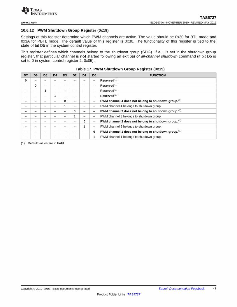
47
TAS5727www.ti.com SLOS670A –NOVEMBER 2010–REVISED MAY 2016
Product Folder Links: TAS5727
Submit Documentation FeedbackCopyright © 2010–2016, Texas Instruments Incorporated
(1) Default values are in bold.
10.6.12 PWM Shutdown Group Register (0x19)Settings of this register determine which PWM channels are active. The value should be 0x30 for BTL mode and0x3A for PBTL mode. The default value of this register is 0x30. The functionality of this register is tied to thestate of bit D5 in the system control register.
This register defines which channels belong to the shutdown group (SDG). If a 1 is set in the shutdown groupregister, that particular channel is not started following an exit out of all-channel shutdown command (if bit D5 isset to 0 in system control register 2, 0x05).
Table 17. PWM Shutdown Group Register (0x19)D7 D6 D5 D4 D3 D2 D1 D0 FUNCTION0 – – – – – – – Reserved (1)
– 0 – – – – – – Reserved (1)
– – 1 – – – – – Reserved (1)
– – – 1 – – – – Reserved (1)
– – – – 0 – – – PWM channel 4 does not belong to shutdown group. (1)
– – – – 1 – – – PWM channel 4 belongs to shutdown group.– – – – – 0 – – PWM channel 3 does not belong to shutdown group. (1)
– – – – – 1 – – PWM channel 3 belongs to shutdown group.– – – – – – 0 – PWM channel 2 does not belong to shutdown group. (1)
– – – – – – 1 – PWM channel 2 belongs to shutdown group.– – – – – – – 0 PWM channel 1 does not belong to shutdown group. (1)
– – – – – – – 1 PWM channel 1 belongs to shutdown group.

48
TAS5727SLOS670A –NOVEMBER 2010–REVISED MAY 2016 www.ti.com
Product Folder Links: TAS5727
Submit Documentation Feedback Copyright © 2010–2016, Texas Instruments Incorporated
(1) Default values are in bold.(2) Default values are in bold.
10.6.13 Start/Stop Period Register (0x1A)This register is used to control the soft-start and soft-stop period following an enter or exit all-channel shutdowncommand or change in the PDN state. This helps reduce pops and clicks at start-up and shutdown. The timesare only approximate and vary depending on device activity level and I2S clock stability.
Table 18. Start/Stop Period Register (0x1A)D7 D6 D5 D4 D3 D2 D1 D0 FUNCTION0 – – – – – – – SSTIMER enabled (1)
1 – – – – – – – SSTIMER disabled– 0 0 – – – – – Reserved (2)
– – – 0 0 – – – No 50% duty cycle start/stop period– – – 0 1 0 0 0 16.5-ms 50% duty cycle start/stop period– – – 0 1 0 0 1 23.9-ms 50% duty cycle start/stop period– – – 0 1 0 1 0 31.4-ms 50% duty cycle start/stop period– – – 0 1 0 1 1 40.4-ms 50% duty cycle start/stop period– – – 0 1 1 0 0 53.9-ms 50% duty cycle start/stop period– – – 0 1 1 0 1 70.3-ms 50% duty cycle start/stop period– – – 0 1 1 1 0 94.2-ms 50% duty cycle start/stop period– – – 0 1 1 1 1 125.7-ms 50% duty cycle start/stop period (2)
– – – 1 0 0 0 0 164.6-ms 50% duty cycle start/stop period– – – 1 0 0 0 1 239.4-ms 50% duty cycle start/stop period– – – 1 0 0 1 0 314.2-ms 50% duty cycle start/stop period– – – 1 0 0 1 1 403.9-ms 50% duty cycle start/stop period– – – 1 0 1 0 0 538.6-ms 50% duty cycle start/stop period– – – 1 0 1 0 1 703.1-ms 50% duty cycle start/stop period– – – 1 0 1 1 0 942.5-ms 50% duty cycle start/stop period– – – 1 0 1 1 1 1256.6-ms 50% duty cycle start/stop period– – – 1 1 0 0 0 1728.1-ms 50% duty cycle start/stop period– – – 1 1 0 0 1 2513.6-ms 50% duty cycle start/stop period– – – 1 1 0 1 0 3299.1-ms 50% duty cycle start/stop period– – – 1 1 0 1 1 4241.7-ms 50% duty cycle start/stop period– – – 1 1 1 0 0 5655.6-ms 50% duty cycle start/stop period– – – 1 1 1 0 1 7383.7-ms 50% duty cycle start/stop period– – – 1 1 1 1 0 9897.3-ms 50% duty cycle start/stop period– – – 1 1 1 1 1 13,196.4-ms 50% duty cycle start/stop period
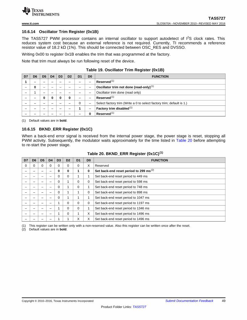
49
TAS5727www.ti.com SLOS670A –NOVEMBER 2010–REVISED MAY 2016
Product Folder Links: TAS5727
Submit Documentation FeedbackCopyright © 2010–2016, Texas Instruments Incorporated
(1) Default values are in bold.
10.6.14 Oscillator Trim Register (0x1B)The TAS5727 PWM processor contains an internal oscillator to support autodetect of I2S clock rates. Thisreduces system cost because an external reference is not required. Currently, TI recommends a referenceresistor value of 18.2 kΩ (1%). This should be connected between OSC_RES and DVSSO.
Writing 0x00 to register 0x1B enables the trim that was programmed at the factory.
Note that trim must always be run following reset of the device.
Table 19. Oscillator Trim Register (0x1B)D7 D6 D5 D4 D3 D2 D1 D0 FUNCTION1 – – – – – – – Reserved (1)
– 0 – – – – – – Oscillator trim not done (read-only) (1)
– 1 – – – – – – Oscillator trim done (read only)– – 0 0 0 0 – – Reserved (1)
– – – – – – 0 – Select factory trim (Write a 0 to select factory trim; default is 1.)– – – – – – 1 – Factory trim disabled (1)
– – – – – – – 0 Reserved (1)
(1) This register can be written only with a non-reserved value. Also this register can be written once after the reset.(2) Default values are in bold.
10.6.15 BKND_ERR Register (0x1C)When a back-end error signal is received from the internal power stage, the power stage is reset, stopping allPWM activity. Subsequently, the modulator waits approximately for the time listed in Table 20 before attemptingto re-start the power stage.
Table 20. BKND_ERR Register (0x1C) (1)
D7 D6 D5 D4 D3 D2 D1 D0 FUNCTION0 0 0 0 0 0 0 X Reserved– – – – 0 0 1 0 Set back-end reset period to 299 ms (2)
– – – – 0 0 1 1 Set back-end reset period to 449 ms– – – – 0 1 0 0 Set back-end reset period to 598 ms– – – – 0 1 0 1 Set back-end reset period to 748 ms– – – – 0 1 1 0 Set back-end reset period to 898 ms– – – – 0 1 1 1 Set back-end reset period to 1047 ms– – – – 1 0 0 0 Set back-end reset period to 1197 ms– – – – 1 0 0 1 Set back-end reset period to 1346 ms– – – – 1 0 1 X Set back-end reset period to 1496 ms– – – – 1 1 X X Set back-end reset period to 1496 ms

50
TAS5727SLOS670A –NOVEMBER 2010–REVISED MAY 2016 www.ti.com
Product Folder Links: TAS5727
Submit Documentation Feedback Copyright © 2010–2016, Texas Instruments Incorporated
(1) Default values are in bold.
10.6.16 Input Multiplexer Register (0x20)This register controls the modulation scheme (AD or BD mode) as well as the routing of I2S audio to the internalchannels.
Table 21. Input Multiplexer Register (0x20)D31 D30 D29 D28 D27 D26 D25 D24 FUNCTION
0 0 0 0 0 0 0 0 Reserved (1)
D23 D22 D21 D20 D19 D18 D17 D16 FUNCTION0 – – – – – – – Channel-1 AD mode (1)
1 – – – – – – – Channel-1 BD mode– 0 0 0 – – – – SDIN-L to channel 1 (1)
– 0 0 1 – – – – SDIN-R to channel 1– 0 1 0 – – – – Reserved– 0 1 1 – – – – Reserved– 1 0 0 – – – – Reserved– 1 0 1 – – – – Reserved– 1 1 0 – – – – Ground (0) to channel 1– 1 1 1 – – – – Reserved– – – – 0 – – – Channel 2 AD mode (1)
– – – – 1 – – – Channel 2 BD mode– – – – – 0 0 0 SDIN-L to channel 2– – – – – 0 0 1 SDIN-R to channel 2 (1)
– – – – – 0 1 0 Reserved– – – – – 0 1 1 Reserved– – – – – 1 0 0 Reserved– – – – – 1 0 1 Reserved– – – – – 1 1 0 Ground (0) to channel 2– – – – – 1 1 1 Reserved
D15 D14 D13 D12 D11 D10 D9 D8 FUNCTION0 1 1 1 0 1 1 1 Reserved (1)
D7 D6 D5 D4 D3 D2 D1 D0 FUNCTION0 1 1 1 0 0 1 0 Reserved (1)

51
TAS5727www.ti.com SLOS670A –NOVEMBER 2010–REVISED MAY 2016
Product Folder Links: TAS5727
Submit Documentation FeedbackCopyright © 2010–2016, Texas Instruments Incorporated
(1) Default values are in bold.
10.6.17 Channel 4 Source Select Register (0x21)This register selects the channel 4 source.
Table 22. Subchannel Control Register (0x21)D31 D30 D29 D28 D27 D26 D25 D24 FUNCTION
0 0 0 0 0 0 0 0 Reserved (1)
D23 D22 D21 D20 D19 D18 D17 D16 FUNCTION0 0 0 0 0 0 0 0 Reserved (1)
D15 D14 D13 D12 D11 D10 D9 D8 FUNCTION0 1 0 0 0 0 1 – Reserved (1)
– – – – – – – 0 (L + R)/2– – – – – – – 1 Left-channel post-BQ (1)
D7 D6 D5 D4 D3 D2 D1 D0 FUNCTION0 0 0 0 0 0 1 1 Reserved (1)
(1) Default values are in bold.
10.6.18 PWM Output MUX Register (0x25)This DAP output mux selects which internal PWM channel is output to the external pins. Any channel can beoutput to any external output pin.
Bits D21–D20: Selects which PWM channel is output to OUT_ABits D17–D16: Selects which PWM channel is output to OUT_BBits D13–D12: Selects which PWM channel is output to OUT_CBits D09–D08: Selects which PWM channel is output to OUT_D
Note that channels are encoded so that channel 1 = 0x00, channel 2 = 0x01, …, channel 4 = 0x03.
Table 23. PWM Output Mux Register (0x25)D31 D30 D29 D28 D27 D26 D25 D24 FUNCTION
0 0 0 0 0 0 0 1 Reserved (1)
D23 D22 D21 D20 D19 D18 D17 D16 FUNCTION0 0 – – – – – – Reserved (1)
– – 0 0 – – – – Multiplex channel 1 to OUT_A (1)
– – 0 1 – – – – Multiplex channel 2 to OUT_A– – 1 0 – – – – Multiplex channel 1 to OUT_A– – 1 1 – – – – Multiplex channel 2 to OUT_A– – – – 0 0 – – Reserved (1)
– – – – – – 0 0 Multiplex channel 1 to OUT_B– – – – – – 0 1 Multiplex channel 2 to OUT_B– – – – – – 1 0 Multiplex channel 1 to OUT_B (1)
– – – – – – 1 1 Multiplex channel 2 to OUT_B

52
TAS5727SLOS670A –NOVEMBER 2010–REVISED MAY 2016 www.ti.com
Product Folder Links: TAS5727
Submit Documentation Feedback Copyright © 2010–2016, Texas Instruments Incorporated
Table 23. PWM Output Mux Register (0x25) (continued)D15 D14 D13 D12 D11 D10 D9 D8 FUNCTION
0 0 – – – – – – Reserved (1)
– – 0 0 – – – – Multiplex channel 1 to OUT_C– – 0 1 – – – – Multiplex channel 2 to OUT_C (1)
– – 1 0 – – – – Multiplex channel 1 to OUT_C– – 1 1 – – – – Multiplex channel 2 to OUT_C– – – – 0 0 – – Reserved (1)
– – – – – – 0 0 Multiplex channel 1 to OUT_D– – – – – – 0 1 Multiplex channel 2 to OUT_D– – – – – – 1 0 Multiplex channel 1 to OUT_D– – – – – – 1 1 Multiplex channel 2 to OUT_D (1)
D7 D6 D5 D4 D3 D2 D1 D0 FUNCTION0 1 0 0 0 1 0 1 Reserved (1)
(1) Default values are in bold.
10.6.19 DRC Control Register (0x46)
Table 24. DRC Control Register (0x46)D31 D30 D29 D28 D27 D26 D25 D24 FUNCTION
0 0 0 0 0 0 0 0 Reserved (1)
D23 D22 D21 D20 D19 D18 D17 D16 FUNCTION0 0 0 0 0 0 0 0 Reserved (1)
D15 D14 D13 D12 D11 D10 D9 D8 FUNCTION0 0 0 0 0 0 0 0 Reserved (1)
D7 D6 D5 D4 D3 D2 D1 D0 FUNCTION0 0 – – – – – – Reserved (1)
– – 0 – – – – – Reserved– – 1 – – – – – Reserved– – – 0 – – – – Reserved (1)
– – – – 0 – – – Reserved (1)
– – – – – 0 – – Reserved (1)
– – – – – – 0 – DRC2 turned OFF (1)
– – – – – – 1 – DRC2 turned ON– – – – – – – 0 DRC1 turned OFF (1)
– – – – – – – 1 DRC1 turned ON

53
TAS5727www.ti.com SLOS670A –NOVEMBER 2010–REVISED MAY 2016
Product Folder Links: TAS5727
Submit Documentation FeedbackCopyright © 2010–2016, Texas Instruments Incorporated
(1) Default values are in bold.
10.6.20 PWM Switching Rate Control Register (0x4F)PWM switching rate should be selected through the register 0x4F before coming out of all-channnel shutdown.
Table 25. PWM Switching Rate Control Register (0x4F)D31 D30 D29 D28 D27 D26 D25 D24 FUNCTION
0 0 0 0 0 0 0 0 Reserved (1)
D23 D22 D21 D20 D19 D18 D17 D16 FUNCTION0 0 0 0 0 0 0 0 Reserved (1)
D15 D14 D13 D12 D11 D10 D9 D8 FUNCTION0 0 0 0 0 0 0 0 Reserved (1)
D7 D6 D5 D4 D3 D2 D1 D0 FUNCTION– – 0 0 – – – – Reserved (1)
– – – – 0 1 1 0 SRC = 6 (1)
– – – – 0 1 1 1 SRC = 7– – – – 1 0 0 0 SRC = 8– – – – 1 0 0 1 SRC = 9– – – – 1 0 1 0 Reserved– – – – 1 1 – – Reserved
(1) Default values are in bold.
10.6.21 Bank Switch and EQ Control (0x50)
Table 26. Bank Switching Command (0x50)D31 D30 D29 D28 D27 D26 D25 D24 FUNCTION
0 0 0 0 0 0 0 0 Reserved (1)
D23 D22 D21 D20 D19 D18 D17 D16 FUNCTION0 0 0 0 0 0 0 0 Reserved (1)
D15 D14 D13 D12 D11 D10 D9 D8 FUNCTION0 0 0 0 0 0 0 0 Reserved (1)
D7 D6 D5 D4 D3 D2 D1 D0 FUNCTION0 EQ ON (1)
1 – – – – – – – EQ OFF (bypass BQ 0–7 of channels 1 and 2)– 0 – – – – – – Reserved (1)
– – 0 – – – – – Ignore bank-mapping in bits D31–D8. Use default mapping. (1)
1 Use bank-mapping in bits D31–D8.– – – 0 – – – – L and R can be written independently. (1)
– – – 1 – – – –L and R are ganged for EQ biquads; a write to the left-channelbiquad is also written to the right-channel biquad. (0x29–0x2F isganged to 0x30–0x36. Also, 0x58–0x5B is ganged to 0x5C–0x5F.
– – – – 0 – – – Reserved (1)
– – – – – 0 0 0 No bank switching. All updates to DAP (1)
– – – – – 0 0 1 Configure bank 1 (32 kHz by default)– – – – – 0 1 X Reserved– – – – – 1 X X Reserved

Copyright © 2016 Texas Instruments Incorporated
54
TAS5727SLOS670A –NOVEMBER 2010–REVISED MAY 2016 www.ti.com
Product Folder Links: TAS5727
Submit Documentation Feedback Copyright © 2010–2016, Texas Instruments Incorporated
11 Application and Implementation
NOTEInformation in the following applications sections is not part of the TI componentspecification, and TI does not warrant its accuracy or completeness. TI’s customers areresponsible for determining suitability of components for their purposes. Customers shouldvalidate and test their design implementation to confirm system functionality.
11.1 Application InformationThe typical connection diagram highlights the required external components and system level connections forproper operation of the device in several popular system examples.
Each of these configurations can be realized using the Evaluation Module (EVM) for the device. These flexiblemodules allow full evaluation of the device in the most common modes of operation. Any design variation can besupported by TI through schematic and layout reviews. Visit http://e2e.ti.com for design assistance and join theaudio amplifier discussion forum for additional information.
11.2 Typical Applications
11.2.1 Stereo Stereo Bridge Tied Load Application
Figure 40. TAS5727 Stereo Application
11.2.1.1 Design RequirementsTable 27 lists the design parameters for this example.
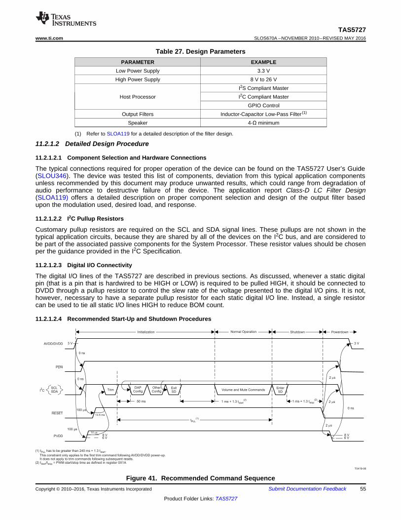
Initialization
50 ms 2 sm
2 sm
2 sm
AVDD/DVDD
PDN
PVDD
RESET
T0419-06
3 V 3 V
0 ns
0 ns
10 sm
100 sμ
13.5 ms
100 sm
6 V 6 V8 V 8 V
I C2 SCL
SDATrim Volume and Mute Commands
ExitSD
EnterSD
DAPConfig
OtherConfig
tPLL
(1)
1 ms + 1.3 tstop
(2)
0 ns
Normal Operation Shutdown Powerdown
(1) t has to be greater than 240 ms + 1.3 t .
This constraint only applies to the first trim command following AVDD/DVDD power-up.It does not apply to trim commands following subsequent resets.
(2) t /t = PWM start/stop time as defined in register 0X1A
PLL start
start stop
1 ms + 1.3 tstart
(2)
55
TAS5727www.ti.com SLOS670A –NOVEMBER 2010–REVISED MAY 2016
Product Folder Links: TAS5727
Submit Documentation FeedbackCopyright © 2010–2016, Texas Instruments Incorporated
(1) Refer to SLOA119 for a detailed description of the filter design.
Table 27. Design ParametersPARAMETER EXAMPLE
Low Power Supply 3.3 VHigh Power Supply 8 V to 26 V
Host ProcessorI2S Compliant MasterI2C Compliant Master
GPIO ControlOutput Filters Inductor-Capacitor Low-Pass Filter (1)
Speaker 4-Ω minimum
11.2.1.2 Detailed Design Procedure
11.2.1.2.1 Component Selection and Hardware Connections
The typical connections required for proper operation of the device can be found on the TAS5727 User’s Guide(SLOU346). The device was tested this list of components, deviation from this typical application componentsunless recommended by this document may produce unwanted results, which could range from degradation ofaudio performance to destructive failure of the device. The application report Class-D LC Filter Design(SLOA119) offers a detailed description on proper component selection and design of the output filter basedupon the modulation used, desired load, and response.
11.2.1.2.2 I2C Pullup Resistors
Customary pullup resistors are required on the SCL and SDA signal lines. These pullups are not shown in thetypical application circuits, because they are shared by all of the devices on the I2C bus, and are considered tobe part of the associated passive components for the System Processor. These resistor values should be chosenper the guidance provided in the I2C Specification.
11.2.1.2.3 Digital I/O Connectivity
The digital I/O lines of the TAS5727 are described in previous sections. As discussed, whenever a static digitalpin (that is a pin that is hardwired to be HIGH or LOW) is required to be pulled HIGH, it should be connected toDVDD through a pullup resistor to control the slew rate of the voltage presented to the digital I/O pins. It is not,however, necessary to have a separate pullup resistor for each static digital I/O line. Instead, a single resistorcan be used to tie all static I/O lines HIGH to reduce BOM count.
11.2.1.2.4 Recommended Start-Up and Shutdown Procedures
Figure 41. Recommended Command Sequence

2 sm
2 sm
AVDD/DVDD
PDN
PVDD
RESET
T0420-05
3 V
8 V
6 V
I C2
2 ms
0 ns
0 ns
0 ns
56
TAS5727SLOS670A –NOVEMBER 2010–REVISED MAY 2016 www.ti.com
Product Folder Links: TAS5727
Submit Documentation Feedback Copyright © 2010–2016, Texas Instruments Incorporated
Figure 42. Power-Loss Sequence
11.2.1.2.4.1 Initialization Sequence
Use the following sequence to power up and initialize the device:1. Hold all digital inputs low and ramp up AVDD/DVDD to at least 3 V.2. Initialize digital inputs and PVDD supply as follows:
– Drive RESET = 0, PDN = 1, and other digital inputs to their desired state while ensuring that all are nevermore than 2.5 V above AVDD/DVDD. Wait at least 100 µs, drive RESET = 1, and wait at least another13.5 ms.
– Ramp up PVDD to at least 8 V while ensuring that it remains below 6 V for at least 100 µs afterAVDD/DVDD reaches 3 V. Then wait at least another 10 µs.
3. Trim oscillator (write 0x00 to register 0x1B) and wait at least 50 ms.4. Configure the DAP through I2C (see User's Guide for typical values).5. Configure remaining registers.6. Exit shutdown (sequence defined below).
11.2.1.2.4.2 Normal Operation
The following are the only events supported during normal operation:1. Writes to master/channel volume registers2. Writes to soft-mute register3. Enter and exit shutdown (sequence defined below)
NOTEEvent 3 is not supported for 240 ms + 1.3 × tstart after trim following AVDD/DVDD power-up ramp (where tstart is specified by register 0x1A).
11.2.1.2.4.3 Shutdown Sequence
Enter:1. Write 0x40 to register 0x05.2. Wait at least 1 ms + 1.3 × tstop (where tstop is specified by register 0x1A).

0.001
0.01
0.1
1
10
20 100 1k 10k 20kFrequency (Hz)
TH
D+
N (
%)
PO = 1WPO = 5WPO = 10W
PVDD = 24VRL = 8ΩTA = 25°C
0 5 10 15 20 25 30 35 400
10
20
30
40
50
60
70
80
90
100
Total Output Power (W)
Effi
cien
cy (
%)
PVDD = 12VPVDD = 18VPVDD = 24V
RL = 8ΩTA = 25°C
57
TAS5727www.ti.com SLOS670A –NOVEMBER 2010–REVISED MAY 2016
Product Folder Links: TAS5727
Submit Documentation FeedbackCopyright © 2010–2016, Texas Instruments Incorporated
3. If desired, reconfigure by returning to step 4 of initialization sequence.
Exit:1. Write 0x00 to register 0x05 (exit shutdown command may not be serviced for as much as 240 ms after trim
following AVDD/DVDD power-up ramp).2. Wait at least 1 ms + 1.3 × tstart (where tstart is specified by register 0x1A).3. Proceed with normal operation.
11.2.1.2.4.4 Power-Down Sequence
Use the following sequence to power down the device and its supplies:1. If time permits, enter shutdown (sequence defined above); else, in case of sudden power loss, assert PDN =
0 and wait at least 2 ms.2. Assert RESET = 0.3. Drive digital inputs low and ramp down PVDD supply as follows:
– Drive all digital inputs low after RESET has been low for at least 2 µs.– Ramp down PVDD while ensuring that it remains above 8 V until RESET has been low for at least 2 µs.
4. Ramp down AVDD/DVDD while ensuring that it remains above 3 V until PVDD is below 6 V and that it isnever more than 2.5 V below the digital inputs.
11.2.1.3 Application Curves
Figure 43. Total Harmonic Distortion + Noise vs FrequencyDashed lines represent thermally limited region.
Figure 44. Efficiency vs Total Output Power

RESET
PDN
SDA
PLL_FLTM
PLL_FLTP
AVDD/DVDD PVDD
3.3 V 8 V–24 V
SCL
DigitalAudio
Source
I CControl
2
ControlInputs
B0264-26
LoopFilter
SDIN
LRCLK
SCLK
MCLK
OUT_A
OUT_B
BST_A
BST_B
OUT_C
OUT_D
BST_C
BST_D
LCPBTL
Copyright © 2016 Texas Instruments Incorporated
58
TAS5727SLOS670A –NOVEMBER 2010–REVISED MAY 2016 www.ti.com
Product Folder Links: TAS5727
Submit Documentation Feedback Copyright © 2010–2016, Texas Instruments Incorporated
11.2.2 Mono Parallel Bridge Tied Load Application
Figure 45. TAS5727 Mono Application
11.2.2.1 Design RequirementsTable 28 lists the design parameters for this example.
(1) Refer to SLOA119 for a detailed description of the filter design.
Table 28. Design ParametersPARAMETER EXAMPLE
Low Power Supply 3.3 VHigh Power Supply 8 V to 26 V
Host ProcessorI2S Compliant MasterI2C Compliant Master
GPIO ControlOutput Filters Inductor-Capacitor Low-Pass Filter (1)
Speaker 2-Ω minimum
11.2.2.2 Detailed Design ProcedureRefer to Detailed Design Procedure.
11.2.2.3 Application CurvesRefer to Application Curves.

59
TAS5727www.ti.com SLOS670A –NOVEMBER 2010–REVISED MAY 2016
Product Folder Links: TAS5727
Submit Documentation FeedbackCopyright © 2010–2016, Texas Instruments Incorporated
12 Power Supply RecommendationsThe TAS5727 requires two power supplies: a low voltage, 3.3 V nominal for the pins DVDD, AVDD, and DRVDD,and a high power supply of 8 V to 24 V for the pin PVDD. There is no requirement for power-up sequencing oflow and high power supplies; however, TI recommends putting the PDN pin to low before removing the lowvoltage power supplies to protect the outputs.
12.1 DVDD and AVDD SuppliesThe AVDD Supply is used to power the analog internal circuit of the device, and needs a well-regulated andfiltered 3.3-V supply voltage. The DVDD Supply is used to power the digital circuitry. DVDD needs a well-regulated and filtered 3.3-V supply voltage.
12.2 PVDD Power SupplyThe TAS5727 class-D audio amplifier requires adequate power supply decoupling to ensure the output totalharmonic distortion (THD) and noise is as low as possible. A good low equivalent-series-resistance (ESR)ceramic capacitor, typically 1 µF, placed as close as possible to the device PVDD leads works best. For filteringlower-frequency noise signals, TI recommends placing a 10 µF or greater capacitor near the audio poweramplifier.
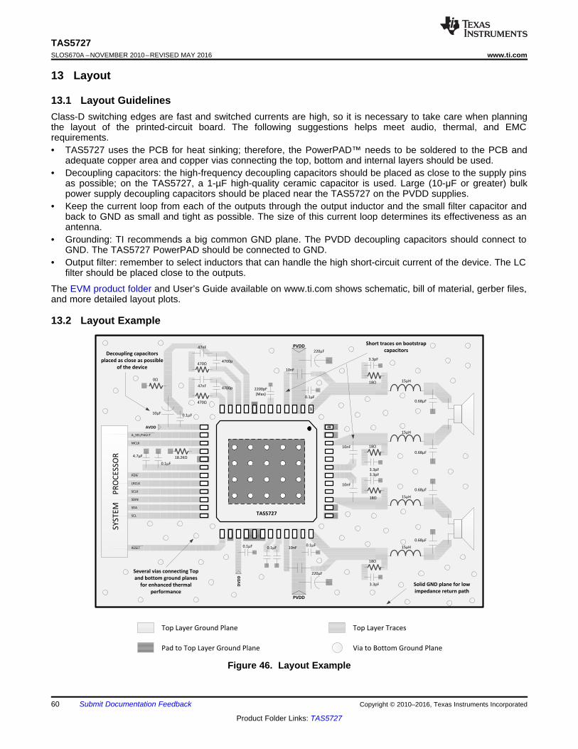
0O
18.2KO
A_SEL/FAULT
MCLK
PDN
SCLK
LRCLK
SDIN
SCL
SDA
RESET
SY
ST
EM
PR
OC
ES
SO
R
DV
DD
AVDD
PVDD
PVDD
Top Layer Ground Plane
Pad to Top Layer Ground Plane Via to Bottom Ground Plane
Top Layer Traces
TAS5727
220µF
10nF
0.1µF
0.1µF
220µF
10nF
10nF
1
48
10nF
2200pF
(Max)
4700p470O
47nF
4700p
470O
47nF
0.1µF10µF
0.1µF
4.7µF
0.1µF 0.1µF
18O
3.3pF
18O
3.3pF
18O
3.3pF
18O
3.3pF
15µH
0.68µF
15µH
0.68µF
15µH
0.68µF
15µH
0.68µF
Decoupling capacitors
placed as close as possible
of the device
Several vias connecting Top
and bottom ground planes
for enhanced thermal
performance
Solid GND plane for low
impedance return path
Short traces on bootstrap
capacitors
60
TAS5727SLOS670A –NOVEMBER 2010–REVISED MAY 2016 www.ti.com
Product Folder Links: TAS5727
Submit Documentation Feedback Copyright © 2010–2016, Texas Instruments Incorporated
13 Layout
13.1 Layout GuidelinesClass-D switching edges are fast and switched currents are high, so it is necessary to take care when planningthe layout of the printed-circuit board. The following suggestions helps meet audio, thermal, and EMCrequirements.• TAS5727 uses the PCB for heat sinking; therefore, the PowerPAD™ needs to be soldered to the PCB and
adequate copper area and copper vias connecting the top, bottom and internal layers should be used.• Decoupling capacitors: the high-frequency decoupling capacitors should be placed as close to the supply pins
as possible; on the TAS5727, a 1-µF high-quality ceramic capacitor is used. Large (10-μF or greater) bulkpower supply decoupling capacitors should be placed near the TAS5727 on the PVDD supplies.
• Keep the current loop from each of the outputs through the output inductor and the small filter capacitor andback to GND as small and tight as possible. The size of this current loop determines its effectiveness as anantenna.
• Grounding: TI recommends a big common GND plane. The PVDD decoupling capacitors should connect toGND. The TAS5727 PowerPAD should be connected to GND.
• Output filter: remember to select inductors that can handle the high short-circuit current of the device. The LCfilter should be placed close to the outputs.
The EVM product folder and User’s Guide available on www.ti.com shows schematic, bill of material, gerber files,and more detailed layout plots.
13.2 Layout Example
Figure 46. Layout Example

61
TAS5727www.ti.com SLOS670A –NOVEMBER 2010–REVISED MAY 2016
Product Folder Links: TAS5727
Submit Documentation FeedbackCopyright © 2010–2016, Texas Instruments Incorporated
14 Device and Documentation Support
14.1 Device Support
14.1.1 Development SupportFor development support, see the following:
TAS57xx GDE
14.2 Documentation Support
14.2.1 Related DocumentationFor related documentation, see the following:• TAS5727 25-W Digital Input Amplifier With EQ and 2-Band DRC, SLOU299• TAS5721-TAS5723EVM User's Guide, SLOU346• Class-D LC Filter Design, SLOA119
14.3 Community ResourcesThe following links connect to TI community resources. Linked contents are provided "AS IS" by the respectivecontributors. They do not constitute TI specifications and do not necessarily reflect TI's views; see TI's Terms ofUse.
TI E2E™ Online Community TI's Engineer-to-Engineer (E2E) Community. Created to foster collaborationamong engineers. At e2e.ti.com, you can ask questions, share knowledge, explore ideas and helpsolve problems with fellow engineers.
Design Support TI's Design Support Quickly find helpful E2E forums along with design support tools andcontact information for technical support.
14.4 TrademarksPowerPAD, E2E are trademarks of Texas Instruments.All other trademarks are the property of their respective owners.
14.5 Electrostatic Discharge CautionThis integrated circuit can be damaged by ESD. Texas Instruments recommends that all integrated circuits be handled withappropriate precautions. Failure to observe proper handling and installation procedures can cause damage.
ESD damage can range from subtle performance degradation to complete device failure. Precision integrated circuits may be moresusceptible to damage because very small parametric changes could cause the device not to meet its published specifications.
14.6 GlossarySLYZ022 — TI Glossary.
This glossary lists and explains terms, acronyms, and definitions.
15 Mechanical, Packaging, and Orderable InformationThe following pages include mechanical, packaging, and orderable information. This information is the mostcurrent data available for the designated devices. This data is subject to change without notice and revision ofthis document. For browser-based versions of this data sheet, refer to the left-hand navigation.

PACKAGE OPTION ADDENDUM
www.ti.com 29-Jan-2016
Addendum-Page 1
PACKAGING INFORMATION
Orderable Device Status(1)
Package Type PackageDrawing
Pins PackageQty
Eco Plan(2)
Lead/Ball Finish(6)
MSL Peak Temp(3)
Op Temp (°C) Device Marking(4/5)
Samples
TAS5727PHP ACTIVE HTQFP PHP 48 250 Green (RoHS& no Sb/Br)
CU NIPDAU Level-3-260C-168 HR 0 to 85 TAS5727
TAS5727PHPR ACTIVE HTQFP PHP 48 1000 Green (RoHS& no Sb/Br)
CU NIPDAU Level-3-260C-168 HR 0 to 85 TAS5727
(1) The marketing status values are defined as follows:ACTIVE: Product device recommended for new designs.LIFEBUY: TI has announced that the device will be discontinued, and a lifetime-buy period is in effect.NRND: Not recommended for new designs. Device is in production to support existing customers, but TI does not recommend using this part in a new design.PREVIEW: Device has been announced but is not in production. Samples may or may not be available.OBSOLETE: TI has discontinued the production of the device.
(2) Eco Plan - The planned eco-friendly classification: Pb-Free (RoHS), Pb-Free (RoHS Exempt), or Green (RoHS & no Sb/Br) - please check http://www.ti.com/productcontent for the latest availabilityinformation and additional product content details.TBD: The Pb-Free/Green conversion plan has not been defined.Pb-Free (RoHS): TI's terms "Lead-Free" or "Pb-Free" mean semiconductor products that are compatible with the current RoHS requirements for all 6 substances, including the requirement thatlead not exceed 0.1% by weight in homogeneous materials. Where designed to be soldered at high temperatures, TI Pb-Free products are suitable for use in specified lead-free processes.Pb-Free (RoHS Exempt): This component has a RoHS exemption for either 1) lead-based flip-chip solder bumps used between the die and package, or 2) lead-based die adhesive used betweenthe die and leadframe. The component is otherwise considered Pb-Free (RoHS compatible) as defined above.Green (RoHS & no Sb/Br): TI defines "Green" to mean Pb-Free (RoHS compatible), and free of Bromine (Br) and Antimony (Sb) based flame retardants (Br or Sb do not exceed 0.1% by weightin homogeneous material)
(3) MSL, Peak Temp. - The Moisture Sensitivity Level rating according to the JEDEC industry standard classifications, and peak solder temperature.
(4) There may be additional marking, which relates to the logo, the lot trace code information, or the environmental category on the device.
(5) Multiple Device Markings will be inside parentheses. Only one Device Marking contained in parentheses and separated by a "~" will appear on a device. If a line is indented then it is a continuationof the previous line and the two combined represent the entire Device Marking for that device.
(6) Lead/Ball Finish - Orderable Devices may have multiple material finish options. Finish options are separated by a vertical ruled line. Lead/Ball Finish values may wrap to two lines if the finishvalue exceeds the maximum column width.
Important Information and Disclaimer:The information provided on this page represents TI's knowledge and belief as of the date that it is provided. TI bases its knowledge and belief on informationprovided by third parties, and makes no representation or warranty as to the accuracy of such information. Efforts are underway to better integrate information from third parties. TI has taken andcontinues to take reasonable steps to provide representative and accurate information but may not have conducted destructive testing or chemical analysis on incoming materials and chemicals.TI and TI suppliers consider certain information to be proprietary, and thus CAS numbers and other limited information may not be available for release.

PACKAGE OPTION ADDENDUM
www.ti.com 29-Jan-2016
Addendum-Page 2
In no event shall TI's liability arising out of such information exceed the total purchase price of the TI part(s) at issue in this document sold by TI to Customer on an annual basis.

TAPE AND REEL INFORMATION
*All dimensions are nominal
Device PackageType
PackageDrawing
Pins SPQ ReelDiameter
(mm)
ReelWidth
W1 (mm)
A0(mm)
B0(mm)
K0(mm)
P1(mm)
W(mm)
Pin1Quadrant
TAS5727PHPR HTQFP PHP 48 1000 330.0 16.4 9.6 9.6 1.5 12.0 16.0 Q2
PACKAGE MATERIALS INFORMATION
www.ti.com 30-Jul-2016
Pack Materials-Page 1

*All dimensions are nominal
Device Package Type Package Drawing Pins SPQ Length (mm) Width (mm) Height (mm)
TAS5727PHPR HTQFP PHP 48 1000 367.0 367.0 38.0
PACKAGE MATERIALS INFORMATION
www.ti.com 30-Jul-2016
Pack Materials-Page 2


IMPORTANT NOTICE
Texas Instruments Incorporated and its subsidiaries (TI) reserve the right to make corrections, enhancements, improvements and otherchanges to its semiconductor products and services per JESD46, latest issue, and to discontinue any product or service per JESD48, latestissue. Buyers should obtain the latest relevant information before placing orders and should verify that such information is current andcomplete. All semiconductor products (also referred to herein as “components”) are sold subject to TI’s terms and conditions of salesupplied at the time of order acknowledgment.TI warrants performance of its components to the specifications applicable at the time of sale, in accordance with the warranty in TI’s termsand conditions of sale of semiconductor products. Testing and other quality control techniques are used to the extent TI deems necessaryto support this warranty. Except where mandated by applicable law, testing of all parameters of each component is not necessarilyperformed.TI assumes no liability for applications assistance or the design of Buyers’ products. Buyers are responsible for their products andapplications using TI components. To minimize the risks associated with Buyers’ products and applications, Buyers should provideadequate design and operating safeguards.TI does not warrant or represent that any license, either express or implied, is granted under any patent right, copyright, mask work right, orother intellectual property right relating to any combination, machine, or process in which TI components or services are used. Informationpublished by TI regarding third-party products or services does not constitute a license to use such products or services or a warranty orendorsement thereof. Use of such information may require a license from a third party under the patents or other intellectual property of thethird party, or a license from TI under the patents or other intellectual property of TI.Reproduction of significant portions of TI information in TI data books or data sheets is permissible only if reproduction is without alterationand is accompanied by all associated warranties, conditions, limitations, and notices. TI is not responsible or liable for such altereddocumentation. Information of third parties may be subject to additional restrictions.Resale of TI components or services with statements different from or beyond the parameters stated by TI for that component or servicevoids all express and any implied warranties for the associated TI component or service and is an unfair and deceptive business practice.TI is not responsible or liable for any such statements.Buyer acknowledges and agrees that it is solely responsible for compliance with all legal, regulatory and safety-related requirementsconcerning its products, and any use of TI components in its applications, notwithstanding any applications-related information or supportthat may be provided by TI. Buyer represents and agrees that it has all the necessary expertise to create and implement safeguards whichanticipate dangerous consequences of failures, monitor failures and their consequences, lessen the likelihood of failures that might causeharm and take appropriate remedial actions. Buyer will fully indemnify TI and its representatives against any damages arising out of the useof any TI components in safety-critical applications.In some cases, TI components may be promoted specifically to facilitate safety-related applications. With such components, TI’s goal is tohelp enable customers to design and create their own end-product solutions that meet applicable functional safety standards andrequirements. Nonetheless, such components are subject to these terms.No TI components are authorized for use in FDA Class III (or similar life-critical medical equipment) unless authorized officers of the partieshave executed a special agreement specifically governing such use.Only those TI components which TI has specifically designated as military grade or “enhanced plastic” are designed and intended for use inmilitary/aerospace applications or environments. Buyer acknowledges and agrees that any military or aerospace use of TI componentswhich have not been so designated is solely at the Buyer's risk, and that Buyer is solely responsible for compliance with all legal andregulatory requirements in connection with such use.TI has specifically designated certain components as meeting ISO/TS16949 requirements, mainly for automotive use. In any case of use ofnon-designated products, TI will not be responsible for any failure to meet ISO/TS16949.
Products ApplicationsAudio www.ti.com/audio Automotive and Transportation www.ti.com/automotiveAmplifiers amplifier.ti.com Communications and Telecom www.ti.com/communicationsData Converters dataconverter.ti.com Computers and Peripherals www.ti.com/computersDLP® Products www.dlp.com Consumer Electronics www.ti.com/consumer-appsDSP dsp.ti.com Energy and Lighting www.ti.com/energyClocks and Timers www.ti.com/clocks Industrial www.ti.com/industrialInterface interface.ti.com Medical www.ti.com/medicalLogic logic.ti.com Security www.ti.com/securityPower Mgmt power.ti.com Space, Avionics and Defense www.ti.com/space-avionics-defenseMicrocontrollers microcontroller.ti.com Video and Imaging www.ti.com/videoRFID www.ti-rfid.comOMAP Applications Processors www.ti.com/omap TI E2E Community e2e.ti.comWireless Connectivity www.ti.com/wirelessconnectivity
Mailing Address: Texas Instruments, Post Office Box 655303, Dallas, Texas 75265Copyright © 2016, Texas Instruments Incorporated