Embed Size (px)
DESCRIPTION
sustituto del HT100-4
Citation preview

SLES127 − FEBRUARY 2005
TM
FEATURES 2×125 W at 10% THD+N Into 4- BTL
2×98 W at 10% THD+N Into 6- BTL
2×76 W at 10% THD+N Into 8- BTL
4×45 W at 10% THD+N Into 3- SE
4×35 W at 10% THD+N Into 4- SE
1×192 W at 10% THD+N Into 3- PBTL
1×240 W at 10% THD+N Into 2- PBTL
>100 dB SNR (A-Weighted)
<0.1% THD+N at 1 W
Thermally Enhanced Package Option:− DKD (36-Pin PSOP3)
High-Efficiency Power Stage (>90%) With140-m Output MOSFETs
Power-On Reset for Protection on Power UpWithout Any Power-Supply Sequencing
Integrated Self-Protection Circuits Including:− Undervoltage− Overtemperature− Overload− Short Circuit
Error Reporting
EMI Compliant When Used WithRecommended System Design
Intelligent Gate Drive
APPLICATIONS Mini/Micro Audio System
DVD Receiver
Home Theater
DESCRIPTION
The TAS5152 is a third-generation, high-performance,integrated stereo digital amplifier power stage withimproved protection system. The TAS5152 is capableof driving a 4-Ω bridge-tied load (BTL) at up to 125 Wper channel with low integrated noise at the output, lowTHD+N performance, and low idle power dissipation.
A low-cost, high-fidelity audio system can be built usinga TI chipset, comprised of a modulator (e.g., TAS5508)and the TAS5152. This system only requires a simplepassive LC demodulation filter to deliver high-quality,high-efficiency audio amplification with proven EMIcompliance. This device requires two power supplies,12 V for GVDD and VDD, and 35 V for PVDD. TheTAS5152 does not require power-up sequencing due tointernal power-on reset. The efficiency of this digitalamplifier is greater than 90% into 6 Ω, which enables theuse of smaller power supplies and heatsinks.
The TAS5152 has an innovative protection systemintegrated on-chip, safeguarding the device against awide range of fault conditions that could damage thesystem. These safeguards are short-circuit protection,overcurrent protection, undervoltage protection, andovertemperature protection. The TAS5152 has a newproprietary current-limiting circuit that reduces thepossibility of device shutdown during high-level musictransients. A new programmable overcurrent detectorallows the use of lower-cost inductors in thedemodulation output filter.
PVDD − Supply Voltage − V
0
10
20
30
40
50
60
70
80
90
100
110
120
130
0 5 10 15 20 25 30 35
PO
− O
utpu
t Pow
er −
W
BTL OUTPUT POWER vs SUPPLY VOLTAGE
8 Ω
4 Ω
TC = 75°CTHD+N @ 10%
6 Ω
! "#$ %!& % "! "! '! ! !( ! %% )*&% "!+ %! !!$* $%! !+ $$ "!!&
PurePath Digital and PowerPAD are trademarks of Texas Instruments.Other trademarks are the property of their respective owners.
Please be aware that an important notice concerning availability, standard warranty, and use in critical applications of Texas Instrumentssemiconductor products and disclaimers thereto appears at the end of this data sheet.
www.ti.com
Copyright 2005, Texas Instruments Incorporated

SLES127 − FEBRUARY 2005
www.ti.com
2
These devices have limited built-in ESD protection. The leads should be shorted together or the device placed in conductive foam duringstorage or handling to prevent electrostatic damage to the MOS gates.
GENERAL INFORMATIONThe TAS5152 is available in a 36-pin PSOP3 (DKD)thermally enhanced package. The package contains aheat slug that is located on the top side of the device forconvenient thermal coupling to the heatsink.
123456789101112131415161718
363534333231302928272625242322212019
GVDD_BOTW
SDPWM_A
RESET_ABPWM_B
OC_ADJGND
AGNDVREG
M3M2M1
PWM_CRESET_CD
PWM_DVDD
GVDD_C
GVDD_ABST_APVDD_AOUT_AGND_AGND_BOUT_BPVDD_BBST_BBST_CPVDD_COUT_CGND_CGND_DOUT_DPVDD_DBST_DGVDD_D
DKD PACKAGE(TOP VIEW)
MODE Selection PinsMODE PINS PWM INPUT OUTPUT
CONFIGU-PROTECTION
SCHEMEM3 M2 M1
CONFIGU-RATION
SCHEME
0 0 02N (1) AD/BD
modulation2 channelsBTL output
BTL mode (2)
0 0 1 Reserved
0 1 01N (1) ADmodulation
2 channelsBTL output
BTL mode (2)
0 1 11N (1) ADmodulation
1 channelPBTL output
PBTL mode.Only PWM_Ainput is used.
1 0 01N (1) ADmodulation
4 channelsSE output
Protection workssimilarly to BTLmode (2). Onlydifference in SE
mode is thatOUT_x is Hi-Z
instead of apulldown throughinternal pulldown
resistor.
1 0 1
1 1 0 Reserved
1 1 1
Reserved
(1) The 1N and 2N naming convention is used to indicate the requirednumber of PWM lines to the power stage per channel in a specificmode.
(2) An overload protection (OLP) occurring on A or B causes bothchannels to shut down. An OLP on C or D works similarly. Globalerrors like overtemperature error (OTE), undervoltage protection(UVP) and power-on reset (POR) affect all channels.
Package Heat Dissipation Ratings (1)
PARAMETER TAS5152DKD
RθJC (°C/W)—2 BTL or 4 SEchannels (8 transistors)
1.28
RθJC ⟨°C/W)—1 BTL or 2 SEchannel(s) (4 transistors)
2.56
RθJC (°C/W)—(1 transistor) 8.6
Pad area (2) 80 mm2
(1) JC is junction-to-case, CH is case-to-heatsink.(2) RθCH is an important consideration. Assume a 2-mil thickness of
typical thermal grease between the pad area and the heatsink. TheRθCH with this condition is 0.8°C/W for the DKD package and1.8°C/W for the DDV package.

SLES127 − FEBRUARY 2005
www.ti.com
3
Absolute Maximum Ratingsover operating free-air temperature range unless otherwise noted(1)
TAS5152
VDD to AGND –0.3 V to 13.2 V
GVDD_X to AGND –0.3 V to 13.2 V
PVDD_X to GND_X (2) –0.3 V to 50 V
OUT_X to GND_X (2) –0.3 V to 50 V
BST_X to GND_X (2) –0.3 V to 63.2 V
VREG to AGND –0.3 V to 4.2 V
GND_X to GND –0.3 V to 0.3 V
GND_X to AGND –0.3 V to 0.3 V
GND to AGND –0.3 V to 0.3 V
PWM_X, OC_ADJ, M1, M2, M3 toAGND
–0.3 V to 4.2 V
RESET_X, SD, OTW to AGND –0.3 V to 7 V
Maximum continuous sink current (SD,OTW)
9 mA
Maximum operating junctiontemperature range, TJ
0°C to 125°C
Storage temperature –40C to 125C
Lead temperature, 1,6 mm (1/16 inch)from case for 10 seconds
260C
Minimum pulse width low 50 ns
(1) Stresses beyond those listed under “absolute maximum ratings”may cause permanent damage to the device. These are stressratings only, and functional operation of the device at these or anyother conditions beyond those indicated under “recommendedoperating conditions” is not implied. Exposure to absolute-maximum-rated conditions for extended periods may affect devicereliability.
(2) These voltages represent the dc voltage + peak ac waveformmeasured at the terminal of the device in all conditions.
Ordering Information
TA PACKAGE DESCRIPTION
0°C to 70°C TAS5152DKD 36-pin PSOP3
For the most current specification and packageinformation, see the TI Web site at www.ti.com.

SLES127 − FEBRUARY 2005
www.ti.com
4
Terminal Functions
TERMINALFUNCTION (1) DESCRIPTION
NAME NO.FUNCTION (1) DESCRIPTION
AGND 9 P Analog ground
BST_A 35 P HS bootstrap supply (BST), external capacitor to OUT_A required
BST_B 28 P HS bootstrap supply (BST), external capacitor to OUT_B required
BST_C 27 P HS bootstrap supply (BST), external capacitor to OUT_C required
BST_D 20 P HS bootstrap supply (BST), external capacitor to OUT_D required
GND 8 P Ground
GND_A 32 P Power ground for half-bridge A
GND_B 31 P Power ground for half-bridge B
GND_C 24 P Power ground for half-bridge C
GND_D 23 P Power ground for half-bridge D
GVDD_A 36 P Gate-drive voltage supply requires 0.1-µF capacitor to AGND
GVDD_B 1 P Gate-drive voltage supply requires 0.1-µF capacitor to AGND
GVDD_C 18 P Gate-drive voltage supply requires 0.1-µF capacitor to AGND
GVDD_D 19 P Gate-drive voltage supply requires 0.1-µF capacitor to AGND
M1 13 I Mode selection pin
M2 12 I Mode selection pin
M3 11 I Mode selection pin
OC_ADJ 7 O Analog overcurrent programming pin requires resistor to ground
OTW 2 O Overtemperature warning signal, open drain, active-low
OUT_A 33 O Output, half-bridge A
OUT_B 30 O Output, half-bridge B
OUT_C 25 O Output, half-bridge C
OUT_D 22 O Output, half-bridge D
PVDD_A 34 P Power supply input for half-bridge A requires close decoupling of 0.1-µF capacitor toGND_A
PVDD_B 29 P Power supply input for half-bridge B requires close decoupling of 0.1-µF capacitor toGND_B
PVDD_C 26 P Power supply input for half-bridge C requires close decoupling of 0.1-µF capacitor toGND_C
PVDD_D 21 P Power supply input for half-bridge D requires close decoupling of 0.1-µF capacitor toGND_D
PWM_A 4 I Input signal for half-bridge A
PWM_B 6 I Input signal for half-bridge B
PWM_C 14 I Input signal for half-bridge C
PWM_D 16 I Input signal for half-bridge D
RESET_AB 5 I Reset signal for half-bridge A and half-bridge B, active-low
RESET_CD 15 I Reset signal for half-bridge C and half-bridge D, active-low
SD 3 O Shutdown signal, open drain, active-low
VDD 17 P Power supply for digital voltage regulator requires 0.1-µF capacitor to GND.
VREG 10 P Digital regulator supply filter pin requires 0.1-µF capacitor to AGND(1) I = input, O = Output, P = Power

SLES127 − FEBRUARY 2005
www.ti.com
5
SYSTEM BLOCK DIAGRAM
2nd-Order L-COutput Filter
for EachHalf-Bridge
BootstrapCapacitors
2-ChannelH-Bridge
BTL Mode
SystemMicrocontroller
OUT_A
OUT_B
OUT_C
OUT_D
BST_A
BST_B
BST_C
BST_D
RESET_ABRESET_CD
SystemPowerSupply
HardwireMode
Control
PVDD
GVDD (12 V)/VDD (12 V)
GND
HardwireOC Limit
M1
M3
PVDDPowerSupply
Decoupling
35 V
12 V
GND
VAC
PWM_A
PWM_C
PWM_D
PWM_B
VALID
M2
Left-Channel
Output
Right-Channel
Output
InputH-Bridge 1
InputH-Bridge 2
GVDDVDD
VREGPower Supply
Decoupling
4
PV
DD
_A, B
, C, D
GN
D_A
, B, C
, D
GV
DD
_A, B
, C, D
4 4
VD
D
GN
D
VR
EG
AG
ND
OC
_AD
J
BootstrapCapacitors
2nd-Order L-COutput Filter
for EachHalf-Bridge
SD
OT
W
OutputH-Bridge 2
OutputH-Bridge 1
OTW
SD
TAS5508

SLES127 − FEBRUARY 2005
www.ti.com
6
FUNCTIONAL BLOCK DIAGRAM
Temp.Sense
M1
M2
RESET_AB
SD
OTW
AGND
OC_ADJ
VREG VREG
VDD
M3
PowerOn
Reset
Under-voltage
Protection
GND
PWM_D OUT_D
GND_D
PVDD_D
BST_D
TimingGateDrive
PWMRcv.
OverloadProtection
Isense
GVDD_D
RESET_CD
4
Protectionand
I/O Logic
PWM_C OUT_C
GND_C
PVDD_C
BST_C
TimingGateDrive
Ctrl.PWMRcv.
GVDD_C
PWM_B OUT_B
GND_B
PVDD_B
BST_B
TimingGateDrive
Ctrl.PWMRcv.
GVDD_B
PWM_A OUT_A
GND_A
PVDD_A
BST_A
TimingGateDrive
Ctrl.PWMRcv.
GVDD_A
Ctrl.
BTL/PBTL−ConfigurationPulldown Resistor
BTL/PBTL−ConfigurationPulldown Resistor
BTL/PBTL−ConfigurationPulldown Resistor
BTL/PBTL−ConfigurationPulldown Resistor
Internal PullupResistors to VREG

SLES127 − FEBRUARY 2005
www.ti.com
7
RECOMMENDED OPERATING CONDITIONSCONDITIONS MIN NOM MAX UNIT
PVDD_x Half-bridge supply DC supply voltage 0 35 37 V
GVDD_xSupply for logic regulators and gate-drive
circuitryDC supply voltage 10.8 12 13.2 V
VDD Digital regulator input DC supply voltage 10.8 12 13.2 V
RL (BTL) Output filter: L = 10 µH, C = 470 nF 3 4
RL (SE) Load impedanceOutput filter: L = 10 µH, C = 470 nFOutput AD modulation, switchingfrequency > 350 kHz
2 3 ΩRL (PBTL)
Load impedance Output AD modulation, switchingfrequency > 350 kHz 1.5 2
Ω
LOutput (BTL)Minimum output inductance under
10
LOutput (SE) Output-filter inductanceMinimum output inductance undershort-circuit condition
10 µH
LOutput (PBTL)
Output-filter inductance short-circuit condition10
µH
FPWM PWM frame rate 192 384 432 kHz
TJ Junction temperature 0 125 C
AUDIO SPECIFICATIONS (BTL)PVDD_X = 35 V, GVDD = VDD = 12 V, BTL mode, RL = 4 Ω, audio frequency = 1 kHz, AES17 filter, FPWM = 384 kHz, case temperature = 75°C,unless otherwise noted. Audio performance is recorded as a chipset, using TAS5508 PWM processor with an effective modulation index limit of96.1%. All performance is in accordance with recommended operating conditions unless otherwise specified.
SYMBOL PARAMETER CONDITIONSTAS5152
UNITSYMBOL PARAMETER CONDITIONSMIN TYP MAX
UNIT
RL = 4 Ω,10% THD, clipped inputsignal
125
RL = 6 Ω,10% THD, clipped inputsignal
98
Po Power output per channel
RL = 8 Ω,10% THD, clipped inputsignal
76
WPo Power output per channelRL = 4 Ω, 0 dBFS, unclipped inputsignal
96W
RL = 6 Ω, 0 dBFS, unclipped inputsignal
72
RL = 8 Ω, 0 dBFS, unclipped inputsignal
57
THD+N Total harmonic distortion + noise0 dBFS 0.3
%THD+N Total harmonic distortion + noise1 W 0.1
%
Vn Output integrated noise A-weighted 145 µV
SNR Signal-to-noise ratio (1) A-weighted 102 dB
DNR Dynamic range
A-weighted, input level = –60 dBFSusing TAS5508 modulator
102 dB
DNR Dynamic rangeA-weighted, input level = –60 dBFSusing TAS5518 modulator
110 dB
Pidle Power dissipation due to idle losses (IPVDDx) PO = 0 W, 2 channels switching (2) 2 W(1) SNR is calculated relative to 0-dBFS input level.(2) Actual system idle losses are affected by core losses of output inductors.

SLES127 − FEBRUARY 2005
www.ti.com
8
AUDIO SPECIFICATIONS (Single-Ended Output)PVDD_X = 35 V, GVDD = VDD = 12 V, SE mode, RL = 4 Ω, audio frequency = 1 kHz, AES17 filter, FPWM = 384 kHz, case temperature = 75°C,unless otherwise noted. Audio performance is recorded as a chipset, using TAS5086 PWM processor with an effective modulation index limit of96.1%. All performance is in accordance with recommended operating conditions unless otherwise specified.
SYMBOL PARAMETER CONDITIONSTAS5152
UNITSYMBOL PARAMETER CONDITIONSMIN TYP MAX
UNIT
RL = 3 Ω,10% THD, clipped inputsignal
45
Po Power output per channel
RL = 4 Ω,10% THD, clipped inputsignal
35
WPo Power output per channelRL = 3 Ω, 0 dBFS, unclipped inputsignal
35W
RL = 4 Ω, 0 dBFS, unclipped inputsignal
25
THD+N Total harmonic distortion + noise0 dBFS 0.2
%THD+N Total harmonic distortion + noise1 W 0.1
%
Vn Output integrated noise A-weighted 90 µV
SNR Signal-to-noise ratio (1) A-weighted 100 dB
DNR Dynamic rangeA-weighted, input level = –60 dBFSusing TAS5508 modulator
100 dB
Pidle Power dissipation due to idle losses (IPVDDx) PO = 0 W, 4 channels switching (2) 2 W(1) SNR is calculated relative to 0-dBFS input level.(2) Actual system idle losses are affected by core losses of output inductors.
AUDIO SPECIFICATIONS (PBTL)PVDD_X = 35 V, GVDD = VDD = 12 V, PBTL mode, RL = 3 Ω, audio frequency = 1 kHz, AES17 filter, FPWM = 384 kHz, case temperature =75°C, unless otherwise noted. Audio performance is recorded as a chipset, using TAS5508 PWM processor with an effective modulation indexlimit of 96.1%. All performance is in accordance with recommended operating conditions unless otherwise specified.
SYMBOL PARAMETER CONDITIONSTAS5152
UNITSYMBOL PARAMETER CONDITIONSMIN TYP MAX
UNIT
RL = 3 Ω,10% THD, clipped inputsignal
192
Po Power output per channel
RL = 2 Ω,10% THD, clipped inputsignal
240
WPo Power output per channelRL = 3 Ω, 0 dBFS, unclipped inputsignal
145W
RL = 2 Ω, 0 dBFS, unclipped inputsignal
190
THD+N Total harmonic distortion + noise0 dBFS 0.2
%THD+N Total harmonic distortion + noise1 W 0.1
%
Vn Output integrated noise A-weighted 160 µV
SNR Signal-to-noise ratio (1) A-weighted 102 dB
DNR Dynamic range
A-weighted, input level = –60 dBFSusing TAS5508 modulator
102 dB
DNR Dynamic rangeA-weighted, input level = –60 dBFSusing TAS5518 modulator
110 dB
Pidle Power dissipation due to idle losses (IPVDDx) PO = 0 W, 1 channel switching (2) 2 W(1) SNR is calculated relative to 0-dBFS input level.(2) Actual system idle losses are affected by core losses of output inductors.

SLES127 − FEBRUARY 2005
www.ti.com
9
ELECTRICAL CHARACTERISTICSRL= 4 Ω. FPWM = 384 kHz, unless otherwise noted. All performance is in accordance with recommended operating conditions unless otherwisespecified.
SYMBOL PARAMETER CONDITIONSTAS5152
SYMBOL PARAMETER CONDITIONSMIN TYP MAX UNITS
Internal Voltage Regulator and Current Consumption
VREG Voltage regulator, only used as a reference node VDD = 12 V 3 3.3 3.6 V
IVDD VDD supply currentOperating, 50% duty cycle 7 17
mAIVDD VDD supply currentIdle, reset mode 6 11
mA
IGVDD_x Gate supply current per half-bridge50% duty cycle 5 16
mAIGVDD_x Gate supply current per half-bridgeReset mode 0.3 1
mA
IPVDD_x Half-bridge idle current
50% duty cycle, withoutoutput filter or load
15 25 mAIPVDD_x Half-bridge idle current
Reset mode, no switching 7 25 µA
Output Stage MOSFETs
RDSon,LS Drain-to-source resistance, LSTJ= 25°C, includesmetallization resistance,GVDD = 12 V
140 155 mΩ
RDSon,HS Drain-to-source resistance, HSTJ= 25°C, includesmetallization resistance,GVDD = 12 V
140 155 mΩ

SLES127 − FEBRUARY 2005
www.ti.com
10
ELECTRICAL CHARACTERISTICS (continued)RL= 4 Ω. FPWM = 384 kHz, unless otherwise noted. All performance is in accordance with recommended operating conditions unless otherwisespecified.
SYMBOL PARAMETER CONDITIONSTAS5152
SYMBOL PARAMETER CONDITIONSMIN TYP MAX UNITS
I/O Protection
Vuvp,G Undervoltage protection limit, GVDD_x 9.8 V
Vuvp,hyst(1) Undervoltage protection hysteresis 250 mV
OTW(1) Overtemperature warning 115 125 135 C
OTWHYST(1) Temperature drop needed below OTW temp. forOTW to be inactive after the OTW event
25 C
OTE(1) Overtemperature error 145 155 165 C
OTE-OTW
differential(1) OTE-OTW differential 30 C
OTEHYST(1) Temperature drop needed below OTE temp. forSD to be released following an OTE event
25 C
OLPC Overload protection counter Fpwm = 384 kHz 1.25 ms
IOC Overcurrent limit protectionResistor-programmable, highend, ROCP = 15 kΩ 8.5 10.8 11.8 A
IOCT Overcurrent response time 210 ns
ROCP OC programming resistor range Resistor tolerance = 5% 15 69 kΩ
RPDInternal pulldown resistor at the output of eachhalf-bridge
Connected when RESET isactive to provide bootstrapcapacitor charge. Not used inSE mode
2.5 kΩ
Static Digital Specifications
VIH High-level input voltage PWM_A, PWM_B, PWM_C,PWM_D, M1, M2, M3,
2 V
VIL Low-level input voltagePWM_D, M1, M2, M3,RESET_AB, RESET_CD 0.8 V
Leakage Input leakage current –10 10 µA
OTW/SHUTDOWN (SD)
RINT_PUInternal pullup resistance, OTW to VREG, SD toVREG
20 26 32 kΩ
Internal pullup resistor 3 3.3 3.6
VOH High-level output voltage External pullup of 4.7 kΩ to5 V
4.5 5V
VOL Low-level output voltage IO = 4 mA 0.2 0.4 V
FANOUT Device fanout OTW , SD No external pullup 30 Devices(1) Specified by design

SLES127 − FEBRUARY 2005
www.ti.com
11
TYPICAL CHARACTERISTICS, BTL CONFIGURATION
Figure 1
PO − Output Power − W
101
TH
D+N
− T
otal
Har
mon
ic D
isto
rtion
+ N
oise
− %
TOTAL HARMONIC DISTORTION + NOISEvs
OUTPUT POWER
0.01
0.1
10
1
TC = 75°CPVDD = 35 VOne Channel
100
4 Ω 6 Ω
8 Ω
PVDD − Supply Voltage − V
0
10
20
30
40
50
60
70
80
90
100
110
120
130
0 5 10 15 20 25 30 35
PO
− O
utpu
t Pow
er −
W
OUTPUT POWERvs
SUPPLY VOLTAGE
8 Ω
4 Ω
TC = 75°CTHD+N @ 10%
6 Ω
Figure 2
Figure 3
PVDD − Supply Voltage − V
0
10
20
30
40
50
60
70
80
90
100
110
120
130
0 5 10 15 20 25 30 35
PO
− O
utpu
t Pow
er −
W
UNCLIPPED OUTPUT POWERvs
SUPPLY VOLTAGE
8 Ω
4 Ω
TC = 75°C
6 Ω
PO − Output Power − W
0
10
20
30
40
50
60
70
80
90
100
0 25 50 75 100 125 150 175 200 225 250
Effi
cien
cy −
%
SYSTEM EFFICIENCYvs
OUTPUT POWER
TC = 25°CTwo Channels
Figure 4
6 Ω4 Ω
8 Ω

SLES127 − FEBRUARY 2005
www.ti.com
12
Figure 5
PO − Output Power − W
0
5
10
15
20
25
30
35
40
45
50
0 25 50 75 100 125 150 175 200 225 250
Pow
er L
oss
− W
SYSTEM POWER LOSSvs
OUTPUT POWER
6 Ω
4 Ω
8 Ω
TC = 25°C
Figure 6
TC − Case Temperature − °C
0
10
20
30
40
50
60
70
80
90
100
110
120
130
140
150
10 20 30 40 50 60 70 80 90 100 110 120
PO
− O
utpu
t Pow
er −
W
SYSTEM OUTPUT POWERvs
CASE TEMPERATURE
8 Ω
4 Ω
THD+N @10%
6 Ω
Figure 7
f − Frequency − kHz
−150
−140
−130
−120
−110
−100
−90
−80
−70
−60
−50
−40
−30
−20
−10
0
0 2 4 6 8 10 12 14 16 18 20 22
Noi
se A
mpl
itude
− d
Br
NOISE AMPLITUDEvs
FREQUENCY
TC = 75°C–60 dB1 kHz
SLES127 − FEBRUARY 2005
www.ti.com
13
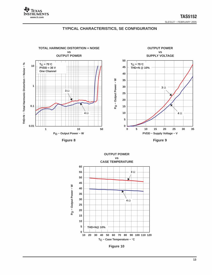
TYPICAL CHARACTERISTICS, SE CONFIGURATION
Figure 8
PO − Output Power − W
101
TH
D+N
− T
otal
Har
mon
ic D
isto
rtion
+ N
oise
− %
TOTAL HARMONIC DISTORTION + NOISEvs
OUTPUT POWER
0.01
0.1
10
1
TC = 75°CPVDD = 35 VOne Channel
3 Ω
4 Ω
50
Figure 9
PVDD − Supply Voltage − V
0
5
10
15
20
25
30
35
40
45
50
0 5 10 15 20 25 30 35
PO
− O
utpu
t Pow
er −
W
OUTPUT POWERvs
SUPPLY VOLTAGE
4 Ω
TC = 75°CTHD+N @ 10%
3 Ω
TC − Case Temperature − °C
0
5
10
15
20
25
30
35
40
45
50
55
60
10 20 30 40 50 60 70 80 90 100 110 120
PO
− O
utpu
t Pow
er −
W
OUTPUT POWERvs
CASE TEMPERATURE
4 Ω
THD+N@ 10%
3 Ω
Figure 10

SLES127 − FEBRUARY 2005
www.ti.com
14
TYPICAL CHARACTERISTICS, PBTL CONFIGURATION
Figure 11
PO − Output Power − W
101
TH
D+N
− T
otal
Har
mon
ic D
isto
rtion
+ N
oise
− %
TOTAL HARMONIC DISTORTION + NOISEvs
OUTPUT POWER
0.01
0.1
10
1
TC = 75°CPVDD = 35 VOne Channel
2 Ω
3 Ω
300100
PVDD − Supply Voltage − V
0
20
40
60
80
100
120
140
160
180
200
220
240
260
0 5 10 15 20 25 30 35
PO
− O
utpu
t Pow
er −
W
OUTPUT POWERvs
SUPPLY VOLTAGE
3 Ω
TC = 75°CTHD+N @ 10%
2 Ω
Figure 12
100
120
140
160
180
200
220
240
260
280
300
10 20 30 40 50 60 70 80 90 100 110 120
Figure 13
TC − Case Temperature − °C
PO
− O
utpu
t Pow
er −
W
SYSTEM OUTPUT POWERvs
CASE TEMPERATURE
THD+N @ 10%
2 Ω
3 Ω

SLES127 − FEBRUARY 2005
www.ti.com
15
VALID
GVDD10 Ω
10 Ω10 µF
100 nF
GVDD1 Ω
100 nF
BKND_ERR
PWM_P_1
PWM_M_1
PWM_P_2
PWM_M_2
PWM_A
PWM_C
OTW
RESET_AB
M2
M3
RESET_CD
VDD
GVDD_C
GVDD_B
PWM_D
VREG
M1
SD
AGND
PWM_B
OC_ADJ
GND
GND_C
OUT_A
BST_A
OUT_B
BST_B
PVDD_B
PVDD_A
BST_C
PVDD_C
OUT_C
GND_A
GND_B
OUT_D
PVDD_D
BST_D
36
35
34
33
23
19
20
21
22
24
25
26
27
28
32
31
30
29
GND_D
GVDD_D
GVDD_A
13
14
15
16
17
18
1
2
3
4
5
6
7
8
9
10
11
12
Microcontroller
22 kΩ
100 nF
33 nF
33 nF
33 nF
33 nF
100 nF50 V
100 nF50 V
100 nF50 V
1000 µF50 V
PVDD
470 nF100 V
10 µH@10 A
10 nF50 V
10 nF50 V
3.3 Ω
3.3 Ω
100 nF50 V
100 nF50 V
3.3 Ω
10 nF50 V
10 nF50 V
1000 µF50 V
PVDD
3.3 Ω
100 nF50 V
47 µF50 V
47 µF50 V
47 µF50 V
10 µF100 nF
100 nF
100 nF
10 µH@10 A
TAS5152DKD
0 ΩOptional
TAS5508
10 Ω
10 Ω
47 µF50 V
470 nF100 V
10 µH@10 A
10 nF50 V
10 nF50 V
3.3 Ω
3.3 Ω
100 nF50 V
100 nF50 V
10 µH@10 A
Figure 14. Typical Differential (2N) BTL Application With AD Modulation Filters

SLES127 − FEBRUARY 2005
www.ti.com
16
VALID
GVDD10 Ω
10 Ω10 µF
100 nF
GVDD1 Ω
100 nF
BKND_ERR
PWM_P_1
PWM_P_2
PWM_A
PWM_C
OTW
RESET_AB
M2
M3
RESET_CD
VDD
GVDD_C
GVDD_B
PWM_D
VREG
M1
SD
AGND
PWM_B
OC_ADJ
GND
GND_C
OUT_A
BST_A
OUT_B
BST_B
PVDD_B
PVDD_A
BST_C
PVDD_C
OUT_C
GND_A
GND_B
OUT_D
PVDD_D
BST_D
36
35
34
33
23
19
20
21
22
24
25
26
27
28
32
31
30
29
GND_D
GVDD_D
GVDD_A
13
14
15
16
17
18
1
2
3
4
5
6
7
8
9
10
11
12
Microcontroller
22 kΩ
100 nF
33 nF
33 nF
33 nF
100 nF50 V
100 nF50 V
100 nF50 V
1000 µF50 V
PVDD
470 nF100 V
10 µH@10 A
10 nF50 V
10 nF50 V
3.3 Ω
3.3 Ω
100 nF50 V
50 nF100 V
3.3 Ω
10 nF50 V
10 nF50 V
1000 µF50 V
PVDD
3.3 Ω
100 nF50 V
47 µF50 V
47 µF50 V
47 µF50 V
10 µF100 nF
100 nF
100 nF
10 µH@10 A
TAS5152DKD
0 ΩOptional
TAS5508
10 Ω
10 Ω
47 µF50 V
470 nF100 V
10 µH@10 A
10 nF50 V
10 nF50 V
3.3 Ω
3.3 Ω
100 nF50 V
100 nF50 V
10 µH@10 A
33 nF
No connect
No connect
Figure 15. Typical Non-Differential (1N) BTL Application With AD Modulation Filters

SLES127 − FEBRUARY 2005
www.ti.com
17
PVDD/2
PVDD/2
PVDD/2
PVDD/2
VALID
GVDD10 Ω
10 Ω10 µF
100 nF
GVDD1 Ω
100 nF
BKND_ERR
PWM_P_1
PWM_P_2
PWM_P_3
PWM_P_4
PWM_A
PWM_C
OTW
RESET_AB
M2
M3
RESET_CD
VDD
GVDD_C
GVDD_B
PWM_D
VREG
M1
SD
AGND
PWM_B
OC_ADJ
GND
GND_C
OUT_A
BST_A
OUT_B
BST_B
PVDD_B
PVDD_A
BST_C
PVDD_C
OUT_C
GND_A
GND_B
OUT_D
PVDD_D
BST_D
36
35
34
33
23
19
20
21
22
24
25
26
27
28
32
31
30
29
GND_D
GVDD_D
GVDD_A
13
14
15
16
17
18
1
2
3
4
5
6
7
8
9
10
11
12
Microcontroller
39 kΩ
100 nF
33 nF
33 nF
33 nF
33 nF
100 nF50 V
100 nF50 V
100 nF50 V
1000 µF50 V
PVDD
10 µH@10 A
3.3 Ω
10 nF50 V
10 nF50 V
1000 µF50 V
PVDD
3.3 Ω
100 nF50 V
47 µF50 V
47 µF50 V
47 µF50 V
10 µF100 nF
100 nF
100 nF
10 µH@10 A
TAS5152DKD
0 ΩOptional
TAS5508
10 Ω
10 Ω
47 µF50 V
10 µH@10 A
10 µH@10 A
10 nF50 V
3.3 Ω
100 nF100 V
10 nF @ 50 V
3.3 Ω
100 nF100 V
1 µF50 V
A
B
C
D
220 µF50 V
220 µF50 V
PVDD
D
C
2.7 kΩ
10 nF50 V
3.3 Ω
100 nF100 V
10 nF @ 50 V
3.3 Ω
100 nF100 V
1 µF50 V
220 µF50 V
220 µF50 V
PVDD
10 nF50 V
3.3 Ω
100 nF100 V
10 nF @ 50 V
3.3 Ω
100 nF100 V
1 µF50 V
220 µF50 V
220 µF50 V
PVDD
10 nF50 V
3.3 Ω
100 nF100 V
10 nF @ 50 V
3.3 Ω
100 nF100 V
1 µF50 V
220 µF50 V
220 µF50 V
PVDD
2.7 kΩ
2.7 kΩ
2.7 kΩ
A
B
Figure 16. Typical SE Application

SLES127 − FEBRUARY 2005
www.ti.com
18
VALID
GVDD10 Ω
10 Ω10 µF
100 nF
GVDD1 Ω
100 nF
BKND_ERR
PWM_P_1 PWM_A
PWM_C
OTW
RESET_AB
M2
M3
RESET_CD
VDD
GVDD_C
GVDD_B
PWM_D
VREG
M1
SD
AGND
PWM_B
OC_ADJ
GND
GND_C
OUT_A
BST_A
OUT_B
BST_B
PVDD_B
PVDD_A
BST_C
PVDD_C
OUT_C
GND_A
GND_B
OUT_D
PVDD_D
BST_D
36
35
34
33
23
19
20
21
22
24
25
26
27
28
32
31
30
29
GND_D
GVDD_D
GVDD_A
13
14
15
16
17
18
1
2
3
4
5
6
7
8
9
10
11
12
Microcontroller
30 kΩ
100 nF
33 nF
33 nF
33 nF
100 nF50 V
100 nF50 V
100 nF50 V
1000 µF50 V
PVDD
10 µH@10 A
3.3 Ω
10 nF50 V
10 nF50 V
1000 µF50 V
PVDD
3.3 Ω
100 nF50 V
47 µF50 V
47 µF50 V
47 µF50 V
10 µF100 nF
100 nF
100 nF
10 µH@10 A
TAS5152DKD
0 ΩOptional
TAS5508
10 Ω
10 Ω
47 µF50 V
10 µH@10 A
10 µH@10 A
33 nF
PWM_M_1
470 nF63 V
10 nF50 V
10 nF50 V
3.3 Ω
3.3 Ω
100 nF100 V
100 nF100 V
Figure 17. Typical Differential (2N) PBTL Application With AD Modulation Filters

SLES127 − FEBRUARY 2005
www.ti.com
19
VALID
GVDD10 Ω
10 Ω10 µF
100 nF
GVDD1 Ω
100 nF
BKND_ERR
PWM_P_1 PWM_A
PWM_C
OTW
RESET_AB
M2
M3
RESET_CD
VDD
GVDD_C
GVDD_B
PWM_D
VREG
M1
SD
AGND
PWM_B
OC_ADJ
GND
GND_C
OUT_A
BST_A
OUT_B
BST_B
PVDD_B
PVDD_A
BST_C
PVDD_C
OUT_C
GND_A
GND_B
OUT_D
PVDD_D
BST_D
36
35
34
33
23
19
20
21
22
24
25
26
27
28
32
31
30
29
GND_D
GVDD_D
GVDD_A
13
14
15
16
17
18
1
2
3
4
5
6
7
8
9
10
11
12
Microcontroller
30 kΩ
100 nF
33 nF
33 nF
33 nF
100 nF50 V
100 nF50 V
100 nF50 V
1000 µF50 V
PVDD
10 µH@10 A
3.3 Ω
10 nF50 V
10 nF50 V
1000 µF50 V
PVDD
3.3 Ω
100 nF50 V
47 µF50 V
47 µF50 V
47 µF50 V
10 µF100 nF
100 nF
100 nF
10 µH@10 A
TAS5152DKD
0 ΩOptional
TAS5508
10 Ω
10 Ω
47 µF50 V
10 µH@10 A
10 µH@10 A
33 nF
470 nF63 V
10 nF50 V
10 nF50 V
3.3 Ω
3.3 Ω
100 nF100 V
100 nF100 V
No connect
No connect
No connect
Figure 18. Typical Non-Differential (1N) PBTL Application

SLES127 − FEBRUARY 2005
www.ti.com
20
THEORY OF OPERATION
POWER SUPPLIES
To facilitate system design, the TAS5152 needs only a12-V supply in addition to the (typically) 35-V power-stagesupply. An internal voltage regulator provides suitablevoltage levels for the digital and low-voltage analogcircuitry. Additionally, all circuitry requiring a floatingvoltage supply, e.g., the high-side gate drive, isaccommodated by built-in bootstrap circuitry requiringonly a few external capacitors.
In order to provide outstanding electrical and acousticalcharacteristics, the PWM signal path including gate driveand output stage is designed as identical, independenthalf-bridges. For this reason, each half-bridge hasseparate gate drive supply (GVDD_X), bootstrap pins(BST_X), and power-stage supply pins (PVDD_X).Furthermore, an additional pin (VDD) is provided as supplyfor all common circuits. Although supplied from the same12-V source, it is highly recommended to separateGVDD_A, GVDD_B, GVDD_C, GVDD_D, and VDD onthe printed-circuit board (PCB) by RC filters (seeapplication diagram for details). These RC filters providethe recommended high-frequency isolation. Specialattention should be paid to placing all decouplingcapacitors as close to their associated pins as possible. Ingeneral, inductance between the power supply pins anddecoupling capacitors must be avoided. (See referenceboard documentation for additional information.)
For a properly functioning bootstrap circuit, a smallceramic capacitor must be connected from each bootstrappin (BST_X) to the power-stage output pin (OUT_X).When the power−stage output is low, the bootstrapcapacitor is charged through an internal diode connectedbetween the gate-drive power-supply pin (GVDD_X) andthe bootstrap pin. When the power-stage output is high,the bootstrap capacitor potential is shifted above theoutput potential and thus provides a suitable voltagesupply for the high-side gate driver. In an application withPWM switching frequencies in the range 352 kHz to 384kHz, it is recommended to use 33-nF ceramic capacitors,size 0603 or 0805, for the bootstrap supply. These 33-nFcapacitors ensure sufficient energy storage, even duringminimal PWM duty cycles, to keep the high-side powerstage FET (LDMOS) fully turned on during the remainingpart of the PWM cycle. In an application running at areduced switching frequency, generally 192 kHz, thebootstrap capacitor might need to be increased in value.
Special attention should be paid to the power-stage powersupply; this includes component selection, PCBplacement and routing. As indicated, each half-bridge hasindependent power-stage supply pins (PVDD_X). Foroptimal electrical performance, EMI compliance, and
system reliability it is important that each PVDD_X pin isdecoupled with a 100-nF ceramic capacitor placed asclose as possible to each supply pin. It is recommended tofollow the PCB layout of the TAS5152 reference design.For additional information on recommended power supplyand required components, see the application diagramsgiven previously in this data sheet.
The 12-V supply should be from a low-noise,low-output-impedance voltage regulator. Likewise, the35-V power-stage supply is assumed to have low outputimpedance and low noise. The power-supply sequence isnot critical as facilitated by the internal power-on-resetcircuit. Moreover, the TAS5152 is fully protected againsterroneous power-stage turnon due to parasitic gatecharging. Thus, voltage-supply ramp rates (dV/dt) arenon-critical within the specified range (see theRecommended Operating Conditions section of this datasheet).
SYSTEM POWER-UP/POWER-DOWNSEQUENCE
Powering Up
The TAS5152 does not require a power-up sequence. Theoutputs of the H−bridges remain in a high-impedance stateuntil the gate-drive supply voltage (GVDD_X) and VDDvoltage are above the undervoltage protection (UVP)voltage threshold (see the Electrical Characteristicssection of this data sheet). Although not specificallyrequired, it is recommended to hold RESET_AB andRESET_CD in a low state while powering up the device.This allows an internal circuit to charge the externalbootstrap capacitors by enabling a weak pulldown of thehalf-bridge output.
When the TAS5152 is being used with TI PWM modulatorssuch as the TAS5508, no special attention to the state ofRESET_AB and RESET_CD is required, provided that thechipset is configured as recommended.
Powering Down
The TAS5152 does not require a power-down sequence.The device remains fully operational as long as thegate-drive supply (GVDD_X) voltage and VDD voltage areabove the undervoltage protection (UVP) voltagethreshold (see the Electrical Characteristics section of thisdata sheet). Although not specifically required, it is a goodpractice to hold RESET_AB and RESET_CD low duringpower down, thus preventing audible artifacts includingpops or clicks.
When the TAS5152 is being used with TI PWM modulatorssuch as the TAS5508, no special attention to the state ofRESET_AB and RESET_CD is required, provided that thechipset is configured as recommended.

SLES127 − FEBRUARY 2005
www.ti.com
21
ERROR REPORTING
The SD and OTW pins are both active-low, open-drainoutputs. Their function is for protection-mode signaling toa PWM controller or other system-control device.
Any fault resulting in device shutdown is signaled by theSD pin going low. Likewise, OTW goes low when thedevice junction temperature exceeds 125°C (see thefollowing table).
SD OTW DESCRIPTION
0 0 Overtemperature (OTE) or overload (OLP) orundervoltage (UVP)
0 1 Overload (OLP) or undervoltage (UVP)
1 0 Junction temperature higher than 125°C(overtemperature warning)
1 1 Junction temperature lower than 125°C and noOLP or UVP faults (normal operation)
Note that asserting either RESET_AB or RESET_CD lowforces the SD signal high, independent of faults beingpresent. TI recommends to monitoring the OTW signalusing the system microcontroller and responding to anovertemperature warning signal by, e.g., turning down thevolume to prevent further heating of the device resulting indevice shutdown (OTE).
To reduce external component count, an internal pullupresistor to 3.3V is provided on both SD and OTW outputs.Level compliance for 5-V logic can be obtained by addingexternal pullup resistors to 5 V (see the ElectricalCharacteristics section of this data sheet for furtherspecifications).
DEVICE PROTECTION SYSTEM
TAS5152 contains advanced protection circuitry carefullydesigned to facilitate system integration and ease of use,as well as to safeguard the device from permanent failuredue to a wide range of fault conditions such as shortcircuits, overload, overtemperature, and undervoltage.The TAS5152 responds to a fault by immediately settingthe power stage in a high-impedance state (Hi-Z) andasserting the SD pin low. In situations other than overload,the device automatically recovers when the fault conditionhas been removed, i.e., the junction temperature hasdropped or the voltage supply has increased. For highestpossible reliability, recovering from an overload faultrequires external reset of the device (see the Device Resetsection of this data sheet) no sooner than 1 second afterthe shutdown.
Use of TAS5152 in High-Modulation-IndexCapable Systems
This device requires at least 50 ns of low time on the outputper 384-kHz PWM frame rate in order to keep thebootstrap capacitors charged. As an example, if themodulation index is set to 99.2% in the TAS5508, thissetting allows PWM pulse durations down to 20 ns. Thissignal, which does not meet the 50-ns requirement, is sentto the PWM_x pin and this low-state pulse time does notallow the bootstrap capacitor to stay charged. In thissituation, the low voltage across the bootstrap capacitorcan cause a failure of the high-side MOSFET transistor,especially when driving a low-impedance load. TheTAS5152 device requires limiting the TAS5508 modulationindex to 96.1% to keep the bootstrap capacitor chargedunder all signals and loads.
Therefore, TI strongly recommends using a TI PWMprocessor, such as TAS5508 or TAS5086, with themodulation index set at 96.1% to interface with TAS5152.
Overcurrent (OC) Protection With CurrentLimiting and Overload Detection
The device has independent, fast-reacting currentdetectors with programmable trip threshold (OC threshold)on all high-side and low-side power-stage FETs. See thefollowing table for OC-adjust resistor values. The detectoroutputs are closely monitored by two protection systems.The first protection system controls the power stage inorder to prevent the output current from further increasing,i.e., it performs a current-limiting function rather thanprematurely shutting down during combinations ofhigh-level music transients and extreme speaker loadimpedance drops. If the high-current situation persists,i.e., the power stage is being overloaded, a secondprotection system triggers a latching shutdown, resultingin the power stage being set in the high-impedance (Hi-Z)state. Current limiting and overload protection areindependent for the half-bridges A and B and, respectively,C and D. That is, if the bridge-tied load betweenhalf-bridges A and B causes an overload fault, onlyhalf-bridges A and B are shut down.
For the lowest-cost bill of materials in termsof component selection, the OC thresholdmeasure should be limited, considering thepower output requirement and minimumload impedance. Higher-impedance loadsrequire a lower OC threshold.
The demodulation-filter inductor must retainat least 3 µH of inductance at twice the OCthreshold setting.

SLES127 − FEBRUARY 2005
www.ti.com
22
Unfortunately, most inductors have decreasing inductancewith increasing temperature and increasing current(saturation). To some degree, an increase in temperaturenaturally occurs when operating at high output currents,due to core losses and the DC resistance of the inductor’scopper winding. A thorough analysis of inductor saturationand thermal properties is strongly recommended.
Setting the OC threshold too low might cause issues suchas lack of enough output power and/or unexpectedshutdowns due to too-sensitive overload detection.
In general, it is recommended to follow closely the externalcomponent selection and PCB layout as given in theApplication section.
For added flexibility, the OC threshold is programmablewithin a limited range using a single external resistorconnected between the OC_ADJ pin and AGND. (See theElectrical Characteristics section of this data sheet forinformation on the correlation between programming-resistor value and the OC threshold.) It should be notedthat a properly functioning overcurrent detector assumesthe presence of a properly designed demodulation filter atthe power-stage output. Short-circuit protection is notprovided directly at the output pins of the power stage butonly on the speaker terminals (after the demodulationfilter). It is required to follow certain guidelines whenselecting the OC threshold and an appropriatedemodulation inductor:
OC-Adjust Resistor V alues(k)
Max. Current Before OCOccurs (A)
15 10.8
22 9.4
27 8.6
39 6.4
47 6
69 4.7
Overtemperature Protection
The TAS5152 has a two-level temperature-protectionsystem that asserts an active-low warning signal (OTW)when the device junction temperature exceeds 125°C(nominal) and, if the device junction temperature exceeds155°C (nominal), the device is put into thermal shutdown,
resulting in all half-bridge outputs being set in thehigh-impedance state (Hi-Z) and SD being asserted low.OTE is latched in this case. To clear the OTE latch, bothRESET_AB and RESET_CD must be asserted.Thereafter, the device resumes normal operation.
Undervoltage Protection (UVP) and Power-OnReset (POR)
The UVP and POR circuits of the TAS5152 fully protect thedevice in any power-up/down and brownout situation.While powering up, the POR circuit resets the overloadcircuit (OLP) and ensures that all circuits are fullyoperational when the GVDD_X and VDD supply voltagesreach 9.8 V (typical). Although GVDD_X and VDD areindependently monitored, a supply voltage drop below theUVP threshold on any VDD or GVDD_X pin results in allhalf-bridge outputs immediately being set in thehigh-impedance state (Hi-Z) and SD being asserted low.The device automatically resumes operation when allsupply voltages have increased above the UVP threshold.
DEVICE RESET
Two reset pins are provided for independent control ofhalf-bridges A/B and C/D. When RESET_AB is assertedlow, all four power-stage FETs in half-bridges A and B areforced into a high-impedance state (Hi-Z). Likewise,asserting RESET_CD low forces all four power-stageFETs in half-bridges C and D into a high-impedance state.Thus, both reset pins are well suited for hard-muting thepower stage if needed.
In BTL modes, to accommodate bootstrap charging priorto switching start, asserting the reset inputs low enablesweak pulldown of the half-bridge outputs. In the SE mode,the weak pulldowns are not enabled, and it is thereforerecommended to ensure bootstrap capacitor charging byproviding a low pulse on the PWM inputs when reset isasserted high.
Asserting either reset input low removes any faultinformation to be signalled on the SD output, i.e., SD isforced high.
A rising-edge transition on either reset input allows thedevice to resume operation after an overload fault.

SLES127 − FEBRUARY 2005
www.ti.com
23
MECHANICAL DATA

PACKAGING INFORMATION
Orderable Device Status (1) PackageType
PackageDrawing
Pins PackageQty
Eco Plan (2) Lead/Ball Finish MSL Peak Temp (3)
TAS5152DKD ACTIVE SSOP DKD 36 29 Pb-Free(RoHS)
CU SNBI Level-4-260C-72 HR/Level-2-220C-1 YEAR
TAS5152DKDR ACTIVE SSOP DKD 36 500 Pb-Free(RoHS)
CU SNBI Level-4-260C-72 HR/Level-2-220C-1 YEAR
(1) The marketing status values are defined as follows:ACTIVE: Product device recommended for new designs.LIFEBUY: TI has announced that the device will be discontinued, and a lifetime-buy period is in effect.NRND: Not recommended for new designs. Device is in production to support existing customers, but TI does not recommend using this part ina new design.PREVIEW: Device has been announced but is not in production. Samples may or may not be available.OBSOLETE: TI has discontinued the production of the device.
(2) Eco Plan - The planned eco-friendly classification: Pb-Free (RoHS) or Green (RoHS & no Sb/Br) - please checkhttp://www.ti.com/productcontent for the latest availability information and additional product content details.TBD: The Pb-Free/Green conversion plan has not been defined.Pb-Free (RoHS): TI's terms "Lead-Free" or "Pb-Free" mean semiconductor products that are compatible with the current RoHS requirementsfor all 6 substances, including the requirement that lead not exceed 0.1% by weight in homogeneous materials. Where designed to be solderedat high temperatures, TI Pb-Free products are suitable for use in specified lead-free processes.Green (RoHS & no Sb/Br): TI defines "Green" to mean Pb-Free (RoHS compatible), and free of Bromine (Br) and Antimony (Sb) based flameretardants (Br or Sb do not exceed 0.1% by weight in homogeneous material)
(3) MSL, Peak Temp. -- The Moisture Sensitivity Level rating according to the JEDEC industry standard classifications, and peak soldertemperature.
Important Information and Disclaimer:The information provided on this page represents TI's knowledge and belief as of the date that it isprovided. TI bases its knowledge and belief on information provided by third parties, and makes no representation or warranty as to theaccuracy of such information. Efforts are underway to better integrate information from third parties. TI has taken and continues to takereasonable steps to provide representative and accurate information but may not have conducted destructive testing or chemical analysis onincoming materials and chemicals. TI and TI suppliers consider certain information to be proprietary, and thus CAS numbers and other limitedinformation may not be available for release.
In no event shall TI's liability arising out of such information exceed the total purchase price of the TI part(s) at issue in this document sold by TIto Customer on an annual basis.
PACKAGE OPTION ADDENDUM
www.ti.com 30-Mar-2005
Addendum-Page 1


IMPORTANT NOTICE
Texas Instruments Incorporated and its subsidiaries (TI) reserve the right to make corrections, modifications,enhancements, improvements, and other changes to its products and services at any time and to discontinueany product or service without notice. Customers should obtain the latest relevant information before placingorders and should verify that such information is current and complete. All products are sold subject to TI’s termsand conditions of sale supplied at the time of order acknowledgment.
TI warrants performance of its hardware products to the specifications applicable at the time of sale inaccordance with TI’s standard warranty. Testing and other quality control techniques are used to the extent TIdeems necessary to support this warranty. Except where mandated by government requirements, testing of allparameters of each product is not necessarily performed.
TI assumes no liability for applications assistance or customer product design. Customers are responsible fortheir products and applications using TI components. To minimize the risks associated with customer productsand applications, customers should provide adequate design and operating safeguards.
TI does not warrant or represent that any license, either express or implied, is granted under any TI patent right,copyright, mask work right, or other TI intellectual property right relating to any combination, machine, or processin which TI products or services are used. Information published by TI regarding third-party products or servicesdoes not constitute a license from TI to use such products or services or a warranty or endorsement thereof.Use of such information may require a license from a third party under the patents or other intellectual propertyof the third party, or a license from TI under the patents or other intellectual property of TI.
Reproduction of information in TI data books or data sheets is permissible only if reproduction is withoutalteration and is accompanied by all associated warranties, conditions, limitations, and notices. Reproductionof this information with alteration is an unfair and deceptive business practice. TI is not responsible or liable forsuch altered documentation.
Resale of TI products or services with statements different from or beyond the parameters stated by TI for thatproduct or service voids all express and any implied warranties for the associated TI product or service andis an unfair and deceptive business practice. TI is not responsible or liable for any such statements.
Following are URLs where you can obtain information on other Texas Instruments products and applicationsolutions:
Products Applications
Amplifiers amplifier.ti.com Audio www.ti.com/audio
Data Converters dataconverter.ti.com Automotive www.ti.com/automotive
DSP dsp.ti.com Broadband www.ti.com/broadband
Interface interface.ti.com Digital Control www.ti.com/digitalcontrol
Logic logic.ti.com Military www.ti.com/military
Power Mgmt power.ti.com Optical Networking www.ti.com/opticalnetwork
Microcontrollers microcontroller.ti.com Security www.ti.com/security
Telephony www.ti.com/telephony
Video & Imaging www.ti.com/video
Wireless www.ti.com/wireless
Mailing Address: Texas Instruments
Post Office Box 655303 Dallas, Texas 75265
Copyright 2005, Texas Instruments Incorporated


![Finale 2005a - [Untitled1]h).pdf · 2014-02-18 · 4 4 4 4 4 4 4 4 4 4 4 4 4 4 4 4 4 4 4 4 4 4 4 4 4 4 4 4 4 4 4 4 4 4 4 4 4 4 4 4 4 4 4 4 4 4 4 4 4 4 Picc. Flutes Oboe Bassoon Bb](https://img.pdfslide.us/doc/110x75/5b737b707f8b9a95348e2e6f/finale-2005a-untitled1-hpdf-2014-02-18-4-4-4-4-4-4-4-4-4-4-4-4-4-4.jpg)


![Oh Pretty Woman4sc].pdfã ### ### ### ### ### ### ### ### 4 4 4 4 4 4 4 4 4 4 4 4 4 4 4 4 4 4 4 2 4 2 4 2 4 2 4 2 4 2 4 2 4 2 4 2 4 4 4 4 4 4 4 4 4 4 4 4 4 4 4 4](https://img.pdfslide.us/doc/110x75/60cfb349cd0cbb00d32b6774/oh-pretty-woman-4scpdf-4-4-4-4-4-4-4-4-4-4.jpg)