Embed Size (px)
Citation preview
TALKTRONICS UNIVERSAL CAMERA SYSTEM
Model IDS2101-CCD42
Marconi CCD42-40 Supplement
Rev. 1.03, July 2002
TALKTRONICS, INC.Huntington Beach, California, USA (714) 841-0622

Talktronics, Inc. Marconi CCD42-40 Supplement Rev. 1.03 7/02
3
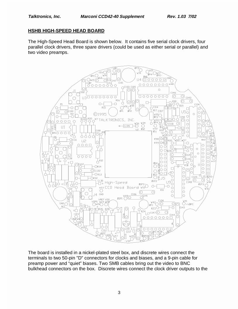
HSHB HIGH-SPEED HEAD BOARD
The High-Speed Head Board is shown below. It contains five serial clock drivers, fourparallel clock drivers, three spare drivers (could be used as either serial or parallel) andtwo video preamps.
The board is installed in a nickel-plated steel box, and discrete wires connect theterminals to two 50-pin "D" connectors for clocks and biases, and a 9-pin cable forpreamp power and “quiet” biases. Two SMB cables bring out the video to BNCbulkhead connectors on the box. Discrete wires connect the clock driver outputs to the
Talktronics, Inc. Marconi CCD42-40 Supplement Rev. 1.03 7/02
4
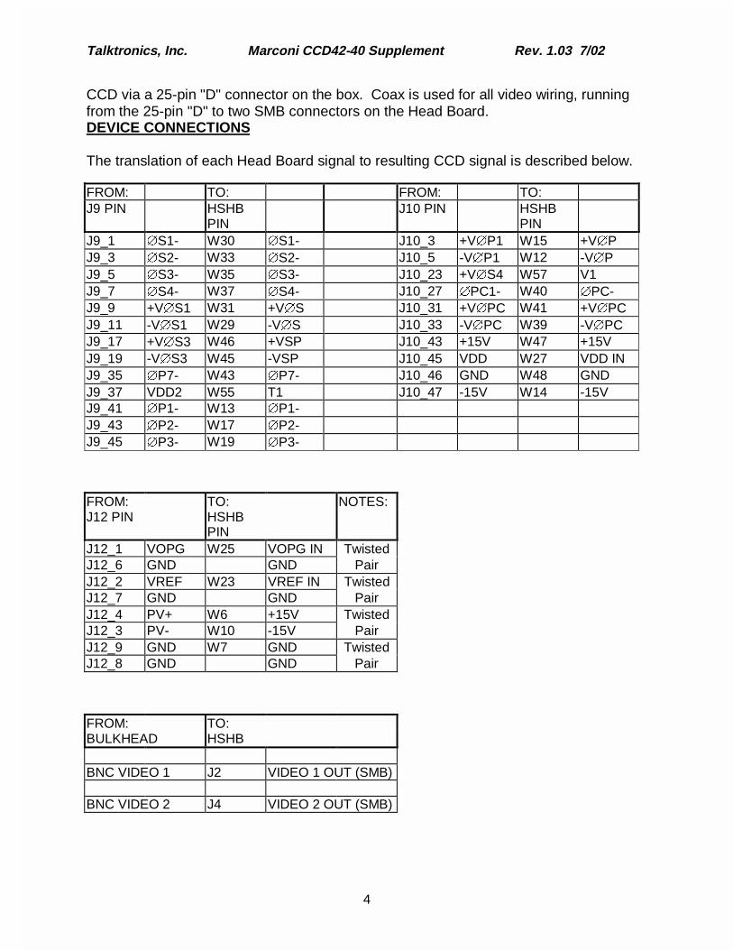
CCD via a 25-pin "D" connector on the box. Coax is used for all video wiring, runningfrom the 25-pin "D" to two SMB connectors on the Head Board.DEVICE CONNECTIONS
The translation of each Head Board signal to resulting CCD signal is described below.
FROM: TO: FROM: TO:J9 PIN HSHB
PINJ10 PIN HSHB
PINJ9_1 �S1- W30 �S1- J10_3 +V�P1 W15 +V�PJ9_3 �S2- W33 �S2- J10_5 -V�P1 W12 -V�PJ9_5 �S3- W35 �S3- J10_23 +V�S4 W57 V1J9_7 �S4- W37 �S4- J10_27 �PC1- W40 �PC-J9_9 +V�S1 W31 +V�S J10_31 +V�PC W41 +V�PCJ9_11 -V�S1 W29 -V�S J10_33 -V�PC W39 -V�PCJ9_17 +V�S3 W46 +VSP J10_43 +15V W47 +15VJ9_19 -V�S3 W45 -VSP J10_45 VDD W27 VDD INJ9_35 �P7- W43 �P7- J10_46 GND W48 GNDJ9_37 VDD2 W55 T1 J10_47 -15V W14 -15VJ9_41 �P1- W13 �P1-J9_43 �P2- W17 �P2-J9_45 �P3- W19 �P3-
FROM: TO: NOTES:J12 PIN HSHB
PINJ12_1 VOPG W25 VOPG IN TwistedJ12_6 GND GND PairJ12_2 VREF W23 VREF IN TwistedJ12_7 GND GND PairJ12_4 PV+ W6 +15V TwistedJ12_3 PV- W10 -15V PairJ12_9 GND W7 GND TwistedJ12_8 GND GND Pair
FROM: TO:BULKHEAD HSHB
BNC VIDEO 1 J2 VIDEO 1 OUT (SMB)
BNC VIDEO 2 J4 VIDEO 2 OUT (SMB)
Talktronics, Inc. Marconi CCD42-40 Supplement Rev. 1.03 7/02
5
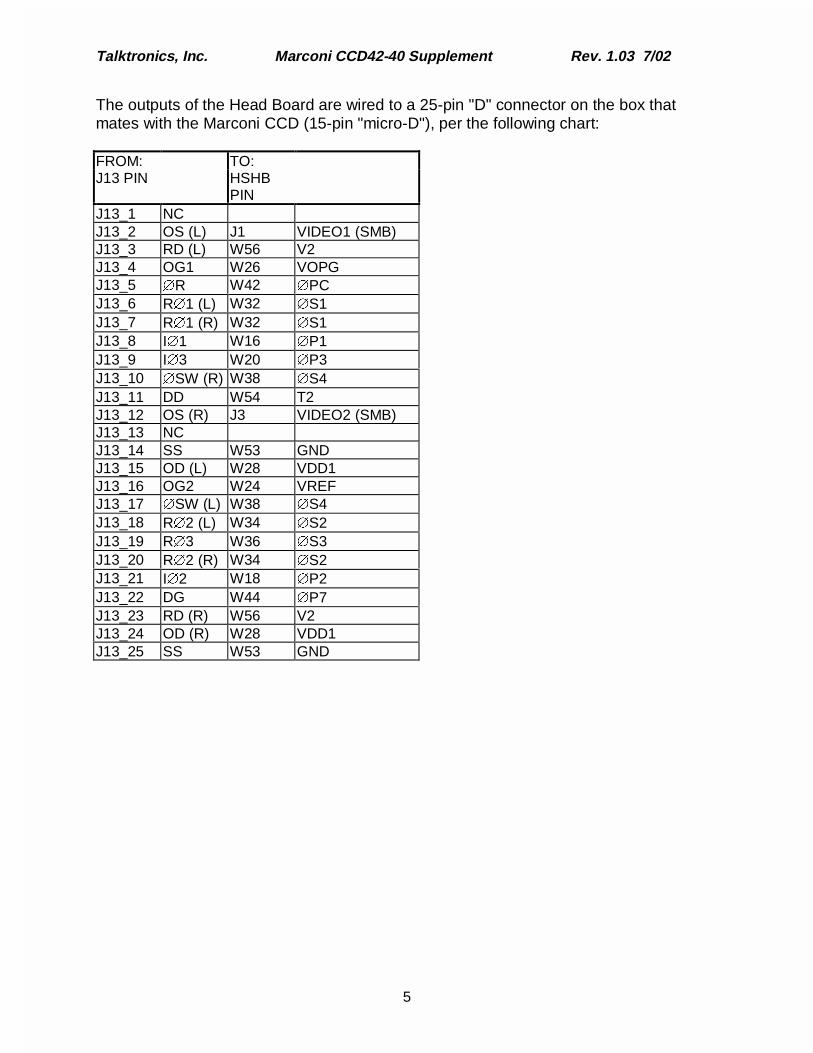
The outputs of the Head Board are wired to a 25-pin "D" connector on the box thatmates with the Marconi CCD (15-pin "micro-D"), per the following chart:
FROM: TO:J13 PIN HSHB
PINJ13_1 NCJ13_2 OS (L) J1 VIDEO1 (SMB)J13_3 RD (L) W56 V2J13_4 OG1 W26 VOPGJ13_5 �R W42 �PCJ13_6 R�1 (L) W32 �S1J13_7 R�1 (R) W32 �S1J13_8 I�1 W16 �P1J13_9 I�3 W20 �P3J13_10 �SW (R) W38 �S4J13_11 DD W54 T2J13_12 OS (R) J3 VIDEO2 (SMB)J13_13 NCJ13_14 SS W53 GNDJ13_15 OD (L) W28 VDD1J13_16 OG2 W24 VREFJ13_17 �SW (L) W38 �S4J13_18 R�2 (L) W34 �S2J13_19 R�3 W36 �S3J13_20 R�2 (R) W34 �S2J13_21 I�2 W18 �P2J13_22 DG W44 �P7J13_23 RD (R) W56 V2J13_24 OD (R) W28 VDD1J13_25 SS W53 GND
Talktronics, Inc. Marconi CCD42-40 Supplement Rev. 1.03 7/02
6
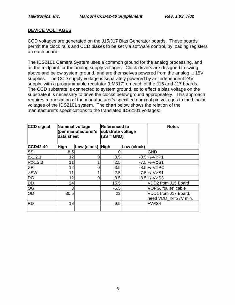
DEVICE VOLTAGES
CCD voltages are generated on the J15/J17 Bias Generator boards. These boardspermit the clock rails and CCD biases to be set via software control, by loading registerson each board.
The IDS2101 Camera System uses a common ground for the analog processing, andas the midpoint for the analog supply voltages. Clock drivers are designed to swingabove and below system ground, and are themselves powered from the analog �15Vsupplies. The CCD supply voltage is separately powered by an independent 24Vsupply, with a programmable regulator (LM317) on each of the J15 and J17 boards.The CCD substrate is connected to system ground, so to effect a bias voltage on thesubstrate it is necessary to drive the clocks below ground appropriately. This approachrequires a translation of the manufacturer’s specified nominal pin voltages to the bipolarvoltages of the IDS2101 system. The chart below shows the relation of themanufacturer’s specifications to the translated IDS2101 voltages:
CCD signal Nominal voltage Referenced to Notes(per manufacturer'sdata sheet
substrate voltage(SS = GND)
CCD42-40 High Low (clock) High Low (clock)SS 8.5 0 GNDI�1,2,3 12 0 3.5 -8.5 +/-V�P1R�1,2,3 11 1 2.5 -7.5 +/-V�S1�R 12 0 3.5 -8.5 +/-V�PC�SW 11 1 2.5 -7.5 +/-V�S1DG 12 0 3.5 -8.5 +/-V�S3DD 24 15.5 VDD2 from J15 BoardOG 3 -5.5 VOPG, "quiet" cableOD 30.5 22 VDD1 from J17 Board,
need VDD_IN=27V min.RD 18 9.5 +V�S4
Talktronics, Inc. Marconi CCD42-40 Supplement Rev. 1.03 7/02
7
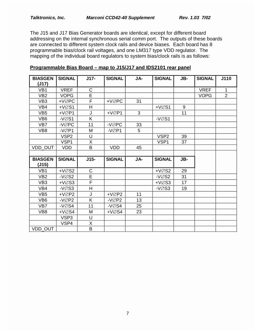
The J15 and J17 Bias Generator boards are identical, except for different boardaddressing on the internal synchronous serial comm port. The outputs of these boardsare connected to different system clock rails and device biases. Each board has 8programmable bias/clock rail voltages, and one LM317 type VDD regulator. Themapping of the individual board regulators to system bias/clock rails is as follows:
Programmable Bias Board – map to J15/J17 and IDS2101 rear panel
BIASGEN SIGNAL J17- SIGNAL JA- SIGNAL JB- SIGNAL J110(J17)VB1 VREF C VREF 1VB2 VOPG E VOPG 2VB3 +V�PC F +V�PC 31VB4 +V�S1 H +V�S1 9VB5 +V�P1 J +V�P1 3 11VB6 -V�S1 K -V�S1VB7 -V�PC 11 -V�PC 33VB8 -V�P1 M -V�P1 5
VSP2 U VSP2 39VSP1 X VSP1 37
VDD_OUT VDD B VDD 45
BIASGEN SIGNAL J15- SIGNAL JA- SIGNAL JB-(J15)VB1 +V�S2 C +V�S2 29VB2 -V�S2 E -V�S2 31VB3 +V�S3 F +V�S3 17VB4 -V�S3 H -V�S3 19VB5 +V�P2 J +V�P2 11VB6 -V�P2 K -V�P2 13VB7 -V�S4 11 -V�S4 25VB8 +V�S4 M +V�S4 23
VSP3 UVSP4 X
VDD_OUT B
Talktronics, Inc. Marconi CCD42-40 Supplement Rev. 1.03 7/02
8
DEVICE TIMING
The serial clocks and overall pixel cycle are created by the J1 and J2 Timing Generatorboards. Registers on each board configure each of the device clocks, system clocksand other pixel-cycle related functions.
The tap chosen for the serial shift register to set the overall pixel cycle period is set by avalue in the SER_TAP register of both the J1 and J2 boards. The identical value mustbe set for both boards. The maximum serial shift register length is 32 t-states (orMCLOCK’s). The DIVIDER register on each board permits lengthening of the pixelcycle by counting multiple MCLOCK’s for each t-state. Normally, the DIVIDER is set toone, and must be identical on both J1 and J2 boards.
Each device or system clock can be configured to default to either the high (inverted) orlow level, and can then be toggled to high or low on any one of the possible pixel cyclet-states. In this example, clocks can be set on any state from 1 to 21. When clocks areto be normally high, the INVERT flag is set for the clock, and the t-states are effectivelyreversed in order for T1 and T2. A clock that is normally low, and is to be set high on t-state 3, then back to low on t-state 6 would have T1 = 3 and T2 = 6. For normally highclocks (inverted), reverse the sequence of T1 and T2: a clock that is normally high(INVERT) and is to go low on t-state 3, then back to high on t-state 6 would have T1 = 6and T2 = 3.
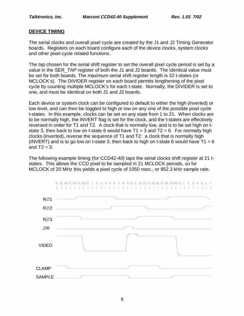
The following example timing (for CCD42-40) taps the serial clocks shift register at 21 t-states. This allows the CCD pixel to be sampled in 21 MCLOCK periods, so forMCLOCK of 20 MHz this yields a pixel cycle of 1050 nsec., or 952.3 kHz sample rate.
R�1
R�2
R�3
�R
VIDEO
SAMPLE
CLAMP
Talktronics, Inc. Marconi CCD42-40 Supplement Rev. 1.03 7/02
9
To calculate the pixel cycle period from the configuration register values for SER_TAPand DIVIDER, and the system clock period:
pixel cycle period = SER_TAP x MCLOCK x DIVIDER= 21 x 50 nsec. x 1 = 1050 nsec.
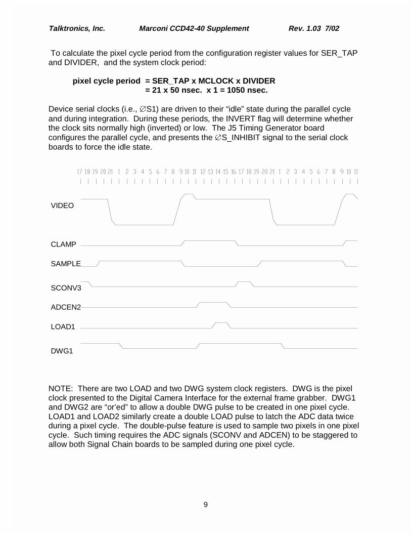
Device serial clocks (i.e., �S1) are driven to their “idle” state during the parallel cycleand during integration. During these periods, the INVERT flag will determine whetherthe clock sits normally high (inverted) or low. The J5 Timing Generator boardconfigures the parallel cycle, and presents the �S_INHIBIT signal to the serial clockboards to force the idle state.
NOTE: There are two LOAD and two DWG system clock registers. DWG is the pixelclock presented to the Digital Camera Interface for the external frame grabber. DWG1and DWG2 are “or’ed” to allow a double DWG pulse to be created in one pixel cycle.LOAD1 and LOAD2 similarly create a double LOAD pulse to latch the ADC data twiceduring a pixel cycle. The double-pulse feature is used to sample two pixels in one pixelcycle. Such timing requires the ADC signals (SCONV and ADCEN) to be staggered toallow both Signal Chain boards to be sampled during one pixel cycle.
VIDEO
SAMPLE
CLAMP
ADCEN2
LOAD1
DWG1
SCONV3
Talktronics, Inc. Marconi CCD42-40 Supplement Rev. 1.03 7/02
10
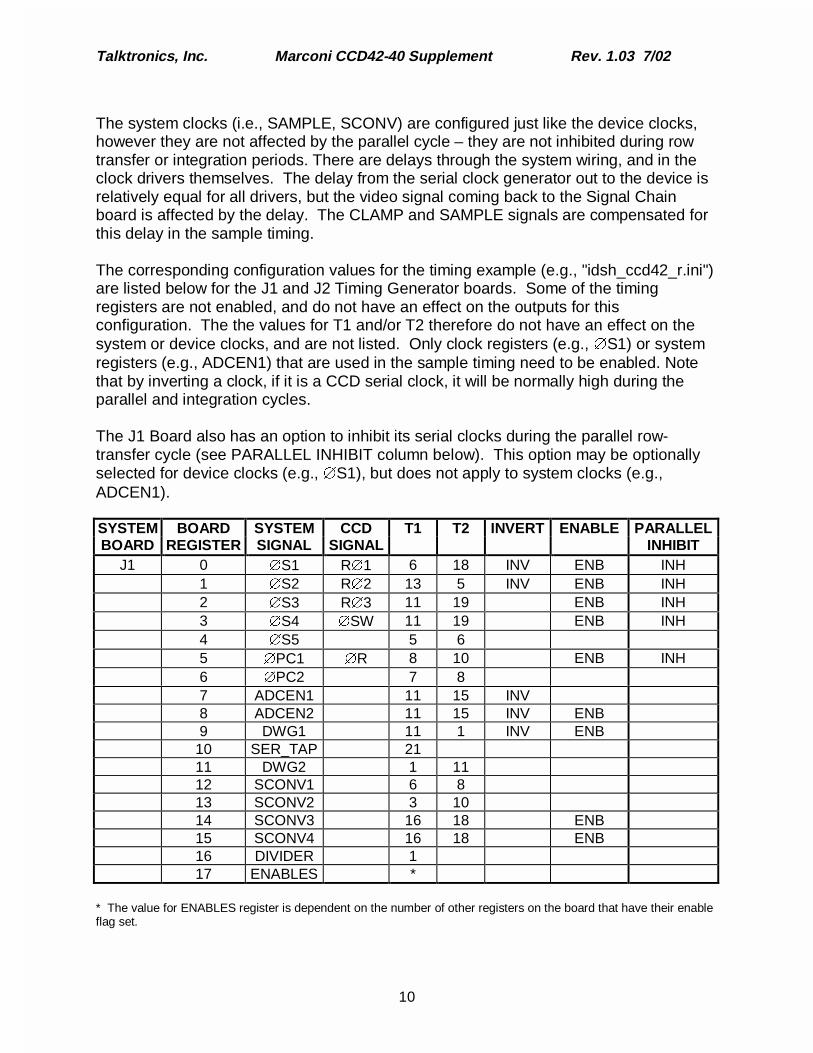
The system clocks (i.e., SAMPLE, SCONV) are configured just like the device clocks,however they are not affected by the parallel cycle – they are not inhibited during rowtransfer or integration periods. There are delays through the system wiring, and in theclock drivers themselves. The delay from the serial clock generator out to the device isrelatively equal for all drivers, but the video signal coming back to the Signal Chainboard is affected by the delay. The CLAMP and SAMPLE signals are compensated forthis delay in the sample timing.
The corresponding configuration values for the timing example (e.g., "idsh_ccd42_r.ini")are listed below for the J1 and J2 Timing Generator boards. Some of the timingregisters are not enabled, and do not have an effect on the outputs for thisconfiguration. The the values for T1 and/or T2 therefore do not have an effect on thesystem or device clocks, and are not listed. Only clock registers (e.g., �S1) or systemregisters (e.g., ADCEN1) that are used in the sample timing need to be enabled. Notethat by inverting a clock, if it is a CCD serial clock, it will be normally high during theparallel and integration cycles.
The J1 Board also has an option to inhibit its serial clocks during the parallel row-transfer cycle (see PARALLEL INHIBIT column below). This option may be optionallyselected for device clocks (e.g., �S1), but does not apply to system clocks (e.g.,ADCEN1).
SYSTEM BOARD SYSTEM CCD T1 T2 INVERT ENABLE PARALLELBOARD REGISTER SIGNAL SIGNAL INHIBIT
J1 0 �S1 R�1 6 18 INV ENB INH1 �S2 R�2 13 5 INV ENB INH2 �S3 R�3 11 19 ENB INH3 �S4 �SW 11 19 ENB INH4 �S5 5 65 �PC1 �R 8 10 ENB INH6 �PC2 7 87 ADCEN1 11 15 INV8 ADCEN2 11 15 INV ENB9 DWG1 11 1 INV ENB
10 SER_TAP 2111 DWG2 1 1112 SCONV1 6 813 SCONV2 3 1014 SCONV3 16 18 ENB15 SCONV4 16 18 ENB16 DIVIDER 117 ENABLES *
* The value for ENABLES register is dependent on the number of other registers on the board that have their enableflag set.
Talktronics, Inc. Marconi CCD42-40 Supplement Rev. 1.03 7/02
11
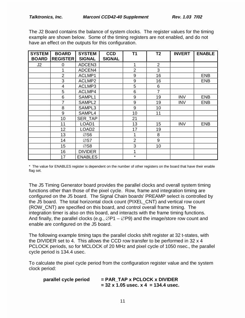
The J2 Board contains the balance of system clocks. The register values for the timingexample are shown below. Some of the timing registers are not enabled, and do nothave an effect on the outputs for this configuration.
SYSTEM BOARD SYSTEM CCD T1 T2 INVERT ENABLEBOARD REGISTER SIGNAL SIGNAL
J2 0 ADCEN3 1 21 ADCEN4 2 32 ACLMP1 9 16 ENB3 ACLMP2 9 16 ENB4 ACLMP3 5 65 ACLMP4 6 76 SAMPL1 9 19 INV ENB7 SAMPL2 9 19 INV ENB8 SAMPL3 9 109 SAMPL4 10 11
10 SER_TAP 2111 LOAD1 13 15 INV ENB12 LOAD2 17 1913 �S6 1 814 �S7 2 915 �S8 3 1016 DIVIDER 117 ENABLES *
* The value for ENABLES register is dependent on the number of other registers on the board that have their enableflag set.
The J5 Timing Generator board provides the parallel clocks and overall system timingfunctions other than those of the pixel cycle. Row, frame and integration timing areconfigured on the J5 board. The Signal Chain boards' PREAMP select is controlled bythe J5 board. The total horizontal clock count (PIXEL_CNT) and vertical row count(ROW_CNT) are specified on this board, and control overall frame timing. Theintegration timer is also on this board, and interacts with the frame timing functions.And finally, the parallel clocks (e.g., �P1 – �P9) and the image/store row count andenable are configured on the J5 board.
The following example timing taps the parallel clocks shift register at 32 t-states, withthe DIVIDER set to 4. This allows the CCD row transfer to be performed in 32 x 4PCLOCK periods, so for MCLOCK of 20 MHz and pixel cycle of 1050 nsec., the parallelcycle period is 134.4 usec.
To calculate the pixel cycle period from the configuration register value and the systemclock period:
parallel cycle period = PAR_TAP x PCLOCK x DIVIDER= 32 x 1.05 usec. x 4 = 134.4 usec.
Talktronics, Inc. Marconi CCD42-40 Supplement Rev. 1.03 7/02
12
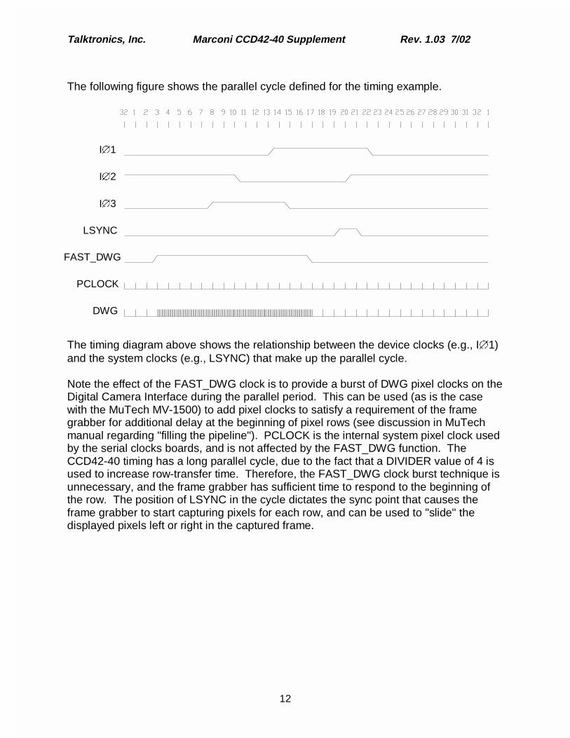
The following figure shows the parallel cycle defined for the timing example.
The timing diagram above shows the relationship between the device clocks (e.g., I�1)and the system clocks (e.g., LSYNC) that make up the parallel cycle.
Note the effect of the FAST_DWG clock is to provide a burst of DWG pixel clocks on theDigital Camera Interface during the parallel period. This can be used (as is the casewith the MuTech MV-1500) to add pixel clocks to satisfy a requirement of the framegrabber for additional delay at the beginning of pixel rows (see discussion in MuTechmanual regarding "filling the pipeline"). PCLOCK is the internal system pixel clock usedby the serial clocks boards, and is not affected by the FAST_DWG function. TheCCD42-40 timing has a long parallel cycle, due to the fact that a DIVIDER value of 4 isused to increase row-transfer time. Therefore, the FAST_DWG clock burst technique isunnecessary, and the frame grabber has sufficient time to respond to the beginning ofthe row. The position of LSYNC in the cycle dictates the sync point that causes theframe grabber to start capturing pixels for each row, and can be used to "slide" thedisplayed pixels left or right in the captured frame.
I�1
I�2
I�3
LSYNC
FAST_DWG
PCLOCK
DWG
Talktronics, Inc. Marconi CCD42-40 Supplement Rev. 1.03 7/02
13
The MuTech Camera Configuration file must have the values for total horizontal clocksand vertical rows in agreement with the configuration of the IDS2101 hardware. It isalways possible to generate more pixel clocks per row, and more rows than specified inthe MuTech camera file, but the DTSpec software will hang if not enough pixel clocksare being generated. In order to determine the total number of pixel clocks per rowwhen FAST_DWG is not used, apply the following equation:
PIXEL_CNT = ( DEVICE PIXELS ) + ( PAR_TAP x DIVIDER )
For each parallel shift register t-state during which FAST_DWG is high, a number ofadditional DWG pixel clocks will be generated for the frame grabber. When the J5board DIVIDER is one (1), the number added will be the same as the length of the serialshift register multiplied by the value for the parallel board DIVIDER, since it countsPCLOCK's, and then divided by two. So for the example, since the J1/J2 serial registerlength is set to 21, and J5 DIVIDER is set to four, 42 DWG pixel clocks will begenerated for each parallel t-state that FAST_DWG is held high.
The MuTech frame grabber requires 16 or 32 pixel clocks to fill its pipeline before validpixels can be grabbed, so the FAST_DWG function allows "padding" the horizontalclocks sufficiently to always capture the first valid device pixel.
To summarize, while the total pixel clocks generated at the Digital Camera Interface israther complex when the FAST_DWG function is utilized, it is only important that moreclocks be generated than specified in the MuTech Camera Configuration file. The"talkccd42.ini" file is a MuTech camera configuration file that has already been designedto work correctly with the "idsh_ccd42_xx.ini" IDS2101 Hardware Configuration fileprovided with the system.
Talktronics, Inc. Marconi CCD42-40 Supplement Rev. 1.03 7/02
14
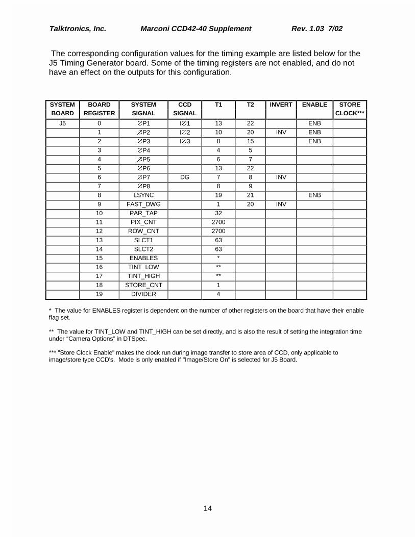
The corresponding configuration values for the timing example are listed below for theJ5 Timing Generator board. Some of the timing registers are not enabled, and do nothave an effect on the outputs for this configuration.
SYSTEM BOARD SYSTEM CCD T1 T2 INVERT ENABLE STOREBOARD REGISTER SIGNAL SIGNAL CLOCK***
J5 0 �P1 I�1 13 22 ENB
1 �P2 I�2 10 20 INV ENB
2 �P3 I�3 8 15 ENB
3 �P4 4 5
4 �P5 6 7
5 �P6 13 22
6 �P7 DG 7 8 INV
7 �P8 8 9
8 LSYNC 19 21 ENB
9 FAST_DWG 1 20 INV
10 PAR_TAP 32
11 PIX_CNT 2700
12 ROW_CNT 2700
13 SLCT1 63
14 SLCT2 63
15 ENABLES *
16 TINT_LOW **
17 TINT_HIGH **
18 STORE_CNT 1
19 DIVIDER 4
* The value for ENABLES register is dependent on the number of other registers on the board that have their enableflag set.
** The value for TINT_LOW and TINT_HIGH can be set directly, and is also the result of setting the integration timeunder “Camera Options” in DTSpec.
*** "Store Clock Enable" makes the clock run during image transfer to store area of CCD, only applicable toimage/store type CCD's. Mode is only enabled if "Image/Store On" is selected for J5 Board.
Talktronics, Inc. Marconi CCD42-40 Supplement Rev. 1.03 7/02
15
IDS2101 HARDWARE CONFIGURATION FILES
The IDS2101 Controller is configured for a particular CCD by downloading binary valuesfrom the host to the controller. The configuration data is transmitted to the controller viathe RS232C serial port. The data is sent in packets that contain a destination address(the board number), the count of data bytes, and the data itself. This data is receivedby the Front Panel Controller in the IDS2101, and then re-transmitted to theprogrammable bias and timing boards via an internal high-speed synchronous serialbus.
The registers of the Programmable Bias Generator boards (J15 and J17), and of theTiming Generator boards (J1, J2 and J5) are described in the Technical ReferenceManual. A text-based configuration file (e.g., "idsh_ccd42_r.ini") contains the values tosend to each programmable board's registers. The configuration file is created by theDTSpec program, using the inputs provided by the user in the "Set Clocks" and "SetBias Voltages" windows. This is the preferred method of file creation. It is also possibleto create or edit the configuration files using a text editor, but this must be done withextreme caution, as it is possible to create illegal values that can cause the IDS2101system to hang.
HOW TO SET UP FOR A CCD
Use the following procedure to change the setup in DTSpec to a different CCD. Theappropriate MuTech Camera Configuration file will be loaded. Next the IDS2101hardware configuration file will be loaded. Then that file will be used to download thenew configuration to the IDS2101 system. Finally, the DTSpec software will bemanually restarted in ALIGN mode to begin capturing images.
CAUTION: It is poss ible that inco rrect voltages or timing information could be loaded into theIDS2101 hardware from the Set System Clocks dialog. Also, a power line glitch could cause asystem malfunction during the download process. It is advisable to remove the CCDwhenever changes are being made in system timing or bias voltages to avoid the poss ibility ofcatastrophic d amage to the CCD. It is recommended to verify CCD s ignals at the so cketbefore re-installing the CCD.
1. Go to the “File” menu, select “Load Camera Config”.2. find the MuTech “\MV-1500\CamCfg” directory. This will be located wherever the
MuTech distribution disk was installed.3. Select the Talktronics camera configuration file for the CCD (e.g., “talkccd42.ini” for
CCD42-40).4. Go to the “File menu, select “Load Setup”.5. Find the IDS2101 Hardware setup file (e.g., “idsh_ccd42_l.ini”). The directory may
need to be changed to the “\Program Files\Talktronics” directory, where DTSpecwas installed.
6. Go to the “Options” menu, select “Set System Clocks”.7. At this point it may be useful to verify that the desired hardware configuration is
selected by inspecting values for the device clocks in the “Set System Clocks”window.
Talktronics, Inc. Marconi CCD42-40 Supplement Rev. 1.03 7/02
16
8. Select “OK” to download the clock configuration and device voltages to the IDS2101system. When download is completed, the IDS2101 system will enter FREE RUNmode and begin generating image frames.
9. Go to the “Start/Stop” menu, select “Start Align Mode”. The system will begingrabbing images.
10. It may be desirable to change the display window size for the selected CCD. To doso, go to the “View” menu and select “Display Options”. Set the “Width” and “Height”as desired. The display window maximum size will be automatically limited to thesize specified in the MuTech camera configuration file for the CCD setup.
CCD42-40 HARDWARE CONFIGURATION FILES
IDS2101 configuration files are provided for different configurations of the CCD:
idsh_ccd42_l.ini -- CCD42-40, readout from left, normal mode, selects SC preamp and ADCEN for left CCD output
idsh_ccd42_r.ini -- CCD42-40, readout from right, normal mode
idsh_ccd42_l_1mhz.ini -- CCD42-40, readout from left, divider set for 1 MHz (approx.)
idsh_ccd42_r_1mhz.ini -- CCD42-40, readout from right, divider set for 1 MHz (approx.)
idsh_ccd42_l_500k.ini -- CCD42-40, readout from left, divider set for 500 kHz (approx.)
idsh_ccd42_r_500k.ini -- CCD42-40, readout from right, divider set for 500 kHz (approx.)
The image/store mode should not be enabled for any of these files, because it is notapplicable to this CCD. For image/store type CCD's, the mode is enabled by selecting"Image/Store Enable" in the "Set System Clocks" window, and then downloading theconfiguration to the IDS2101 hardware.
Talktronics, Inc. Marconi CCD42-40 Supplement Rev. 1.03 7/02
17
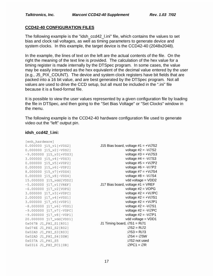
CCD42-40 CONFIGURATION FILES
The following example is the "idsh_ccd42_l.ini" file, which contains the values to setbias and clock rail voltages, as well as timing parameters to generate device andsystem clocks. In this example, the target device is the CCD42-40 (2048x2048).
In the example, the lines of text on the left are the actual contents of the file. On theright the meaning of the text line is provided. The calculation of the hex value for atiming register is made internally by the DTSpec program. In some cases, the valuemay be easily interpreted as the hex equivalent of the decimal value entered by the user(e.g., J5_PIX_COUNT). The device and system clock registers have bit fields that arepacked into a 16 bit value, and are best generated by the DTSpec program. Not allvalues are used to drive the CCD setup, but all must be included in the “.ini” filebecause it is a fixed-format file.
It is possible to view the user values represented by a given configuration file by loadingthe file in DTSpec, and then going to the "Set Bias Voltage" or "Set Clocks" window inthe menu.
The following example is the CCD42-40 hardware configuration file used to generatevideo out the “left” output pin.
idsh_ccd42_l.ini:
[enh_hardware]0.000000 j15_v1[+V0S2] J15 Bias board, voltage #1 = +V�S20.000000 j15_v2[-V0S2] voltage #2 = -V�S2-9.000000 j15_v3[+V0S3] voltage #3 = +V�S33.000000 j15_v4[-V0S3] voltage #4 = -V�S30.000000 j15_v5[+V0P2] voltage #5 = +V�P20.000000 j15_v6[-V0P2] voltage #6 = -V�P28.000000 j15_v7[+V0S4] voltage #7 = +V�S40.000000 j15_v8[-V0S4] voltage #8 = -V�S415.000000 j15_vdd[VDD2] vdd voltage = VDD2-5.000000 j17_v1[VREF] J17 Bias board, voltage #1 = VREF-6.000000 j17_v2[VOPG] voltage #2 = VOPG3.000000 j17_v3[+V0PC] voltage #2 = +V�PC2.000000 j17_v4[+V0S1] voltage #2 = +V�S13.000000 j17_v5[+V0P1] voltage #2 = +V�P1-8.000000 j17_v6[-V0S1] voltage #2 = -V�S1-9.000000 j17_v7[-V0PC] voltage #2 = -V�PC-9.000000 j17_v8[-V0P1] voltage #2 = -V�P120.000000 j17_vdd[VDD1] vdd voltage = VDD10x067B J1_PHI_S1[R01] J1 Timing board, �S1 = R�10x074E J1_PHI_S2[R02] �S2 = R�20x02AD J1_PHI_S3[R03] �S3 = R�30x02AD J1_PHI_S4[0SW] �S4 = �SW0x037A J1_PHI_S5 �S2 not used0x0316 J1_PHI_PC1[0R] �PC1 = �R
Talktronics, Inc. Marconi CCD42-40 Supplement Rev. 1.03 7/02
18
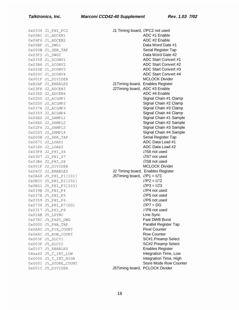
0x0338 J1_PHI_PC2 J1 Timing board, �PC2 not used0x06B1 J1_ADCEN1 ADC #1 Enable0x06F6 J1_ADCEN2 ADC #2 Enable0x06BF J1_DWG1 Data Word Gate #10x000B J1_SER_TAP Serial Register Tap0x03F5 J1_DWG2 Data Word Gate #20x0358 J1_SCONV1 ADC Start Convert #10x03B6 J1_SCONV2 ADC Start Convert #20x020E J1_SCONV3 ADC Start Convert #30x020C J1_SCONV4 ADC Start Convert #40x001F J1_DIVIDER MCLOCK Divider0xB2AF J1_ENABLES J1Timing board, Enables Register0x03FE J2_ADCEN3 J2Timing board, ADC #3 Enable0x03DD J2_ADCEN4 ADC #4 Enable0x02D0 J2_ACLMP1 Signal Chain #1 Clamp0x02D0 J2_ACLMP2 Signal Chain #2 Clamp0x037A J2_ACLMP3 Signal Chain #3 Clamp0x0359 J2_ACLMP4 Signal Chain #4 Clamp0x06ED J2_SAMPL1 Signal Chain #1 Sample0x06ED J2_SAMPL2 Signal Chain #2 Sample0x02F6 J2_SAMPL3 Signal Chain #3 Sample0x02D5 J2_SAMPL4 Signal Chain #4 Sample0x000B J2_SER_TAP Serial Register Tap0x0671 J2_LOAD1 ADC Data Load #10x01ED J2_LOAD2 ADC Data Load #20x03F8 J2_PHI_S6 �S6 not used0x03D7 J2_PHI_S7 �S7 not used0x03B6 J2_PHI_S8 �S8 not used0x001F J2_DIVIDER MCLOCK Divider0x04CC J2_ENABLES J2 Timing board, Enables Register0x0A68 J5_PHI_P1[I01] J5Timing board, �P1 = I�10x0ECC J5_PHI_P2[I02] �P2 = I�20x0B51 J5_PHI_P3[I03] �P3 = I�30x039B J5_PHI_P4 �P4 not used0x037A J5_PHI_P5 �P5 not used0x0359 J5_PHI_P6 �P6 not used0x0738 J5_PHI_P7[DG] �P7 = DG0x0317 J5_PHI_P8 �P8 not used0x01AB J5_LSYNC Line Sync0x07EC J5_FAST_DWG Fast DWB Burst0x0000 J5_PAR_TAP Parallel Register Tap0x0A8C J5_PIX_COUNT Pixel Counter0x0A8C J5_ROW_COUNT Row Counter0x003F J5_SLCT1 SC#1 Preamp Select0x003F J5_SLCT2 SC#2 Preamp Select0x0107 J5_ENABLES Enables Register0Xea60 J5_T_INT_LOW Integration Time, Low0x0000 J5_T_INT_HIGH Integration Time, High0x0001 J5_STORE_COUNT Store Mode Row Counter0x001C J5_DIVIDER J5Timing board, PCLOCK Divider
Talktronics, Inc. Marconi CCD42-40 Supplement Rev. 1.03 7/02
19
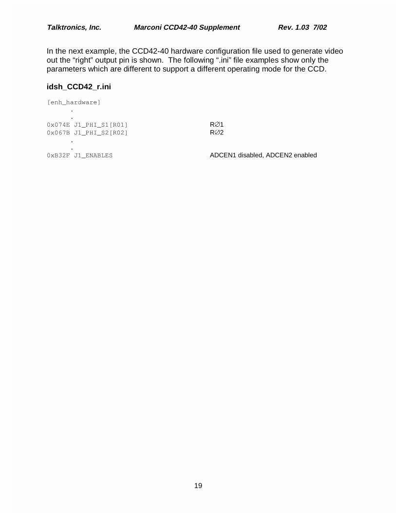
In the next example, the CCD42-40 hardware configuration file used to generate videoout the “right” output pin is shown. The following “.ini” file examples show only theparameters which are different to support a different operating mode for the CCD.
idsh_CCD42_r.ini
[enh_hardware]..
0x074E J1_PHI_S1[R01] R�10x067B J1_PHI_S2[R02] R�2
.
.0xB32F J1_ENABLES ADCEN1 disabled, ADCEN2 enabled
Talktronics, Inc. Marconi CCD42-40 Supplement Rev. 1.03 7/02
20
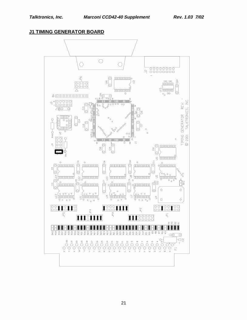
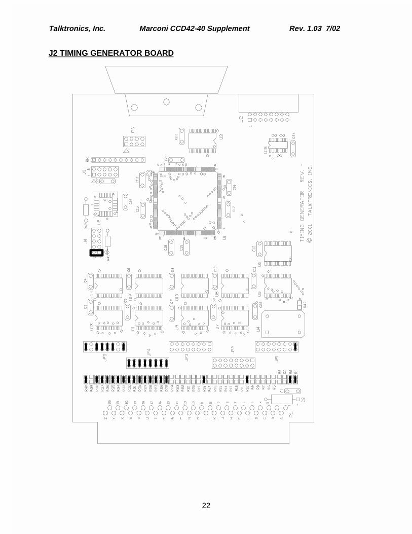
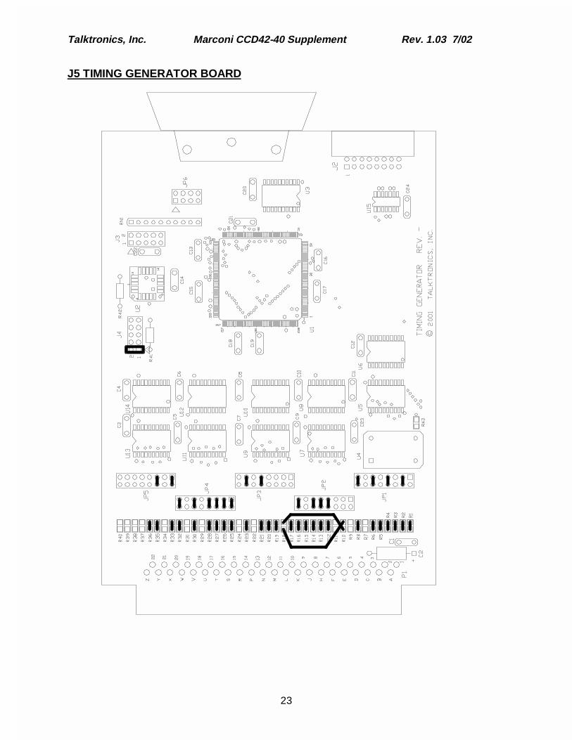
J1, J2 AND J5 TIMING GENERATOR BOARDS
The Timing Generator boards generate each of the system clocks described in theDEVICE TIMING section of this manual (see also Technical Reference manual). ThePCB used for the three timing boards is identical, differing only in the programming ofthe FPGA and the connections to the card cage motherboard. The connections to themotherboard are made by jumpers and SMT resistors on each board. The FPGA candrive or read any pin on the motherboard edge-card connector. The SMT resistors areused as jumpers to connect the edge card pins (most are zero ohm jumpers, but canalso have actual resistance, i.e., for clock damping), while the jumper blocks are used toconnect the outgoing signals of the FPGA to the edge-card connector. An SMT resistorconnects both input and output signals, while the jumper blocks connect only theoutgoing signal. The programming of the FPGA defines whether a signal is input oroutput, and can not be changed by the user.
The hardwired jumpers for each board, together with the FPGA programming, make aparticular board into one of:
J1 – Serial ClocksJ2 – Serial ClocksJ5 – Parallel Clocks
The jumpers are shown for each of the boards in the following figures.
Talktronics, Inc. Marconi CCD42-40 Supplement Rev. 1.03 7/02
21
J1 TIMING GENERATOR BOARD
Talktronics, Inc. Marconi CCD42-40 Supplement Rev. 1.03 7/02
22
J2 TIMING GENERATOR BOARD
Talktronics, Inc. Marconi CCD42-40 Supplement Rev. 1.03 7/02
23
J5 TIMING GENERATOR BOARD
Talktronics, Inc. Marconi CCD42-40 Supplement Rev. 1.03 7/02
24
DEVICE SOCKET TEST DATA
The following pages contain test data from CCD socket pin testing. This test data wascollected with the system running for pin voltages, or with the system powered down forpin resistance. Pin voltages and resistances were measured with the CCD removedprior to changes in hardware or setup.
Note that resistance measurements will vary widely, depending on the type of meterused and its sample current. Also, the measured resistance will vary depending on howlong the system has been without power applied. These values are only representative,and should only be used to determine the presence of major faults. It is very importantthat the CCD output pin not be driving into a short circuit, so this measurement shouldbe made every time that the CCD is to be connected to the head board electronics.
Voltage measurements were taken on an autoranging DC scale, and represent theaverage voltage at a pin. Clock signals are switching at high frequency, so the meterwill only indicate the clock's average voltage.
Talktronics, Inc. Marconi CCD42-40 Supplement Rev. 1.03 7/02
25
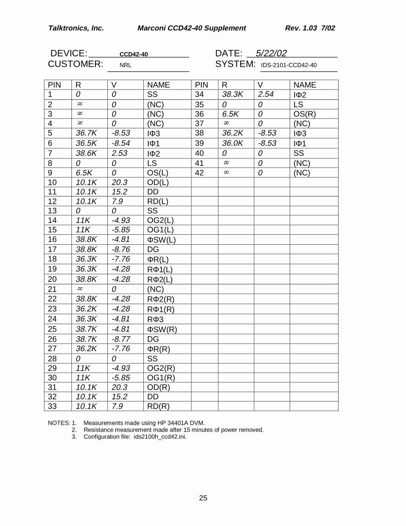
DEVICE: CCD42-40 DATE: 5/22/02CUSTOMER: NRL SYSTEM: IDS-2101-CCD42-40
PIN R V NAME PIN R V NAME1 0 0 SS 34 38.3K 2.54 IΦ22 � 0 (NC) 35 0 0 LS3 � 0 (NC) 36 6.5K 0 OS(R)4 � 0 (NC) 37 � 0 (NC)5 36.7K -8.53 IΦ3 38 36.2K -8.53 IΦ36 36.5K -8.54 IΦ1 39 36.0K -8.53 IΦ17 38.6K 2.53 IΦ2 40 0 0 SS8 0 0 LS 41 � 0 (NC)9 6.5K 0 OS(L) 42 � 0 (NC)10 10.1K 20.3 OD(L)11 10.1K 15.2 DD12 10.1K 7.9 RD(L)13 0 0 SS14 11K -4.93 OG2(L)15 11K -5.85 OG1(L)16 38.8K -4.81 ΦSW(L)17 38.8K -8.76 DG18 36.3K -7.76 ΦR(L)19 36.3K -4.28 RΦ1(L)20 38.8K -4.28 RΦ2(L)21 � 0 (NC)22 38.8K -4.28 RΦ2(R)23 36.2K -4.28 RΦ1(R)24 36.3K -4.81 RΦ325 38.7K -4.81 ΦSW(R)26 38.7K -8.77 DG27 36.2K -7.76 ΦR(R)28 0 0 SS29 11K -4.93 OG2(R)30 11K -5.85 OG1(R)31 10.1K 20.3 OD(R)32 10.1K 15.2 DD33 10.1K 7.9 RD(R)
NOTES: 1. Measurements made using HP 34401A DVM.2. Resistance measurement made after 15 minutes of power removed.3. Configuration file: ids2100h_ccd42.ini.
Talktronics, Inc. Marconi CCD42-40 Supplement Rev. 1.03 7/02
26
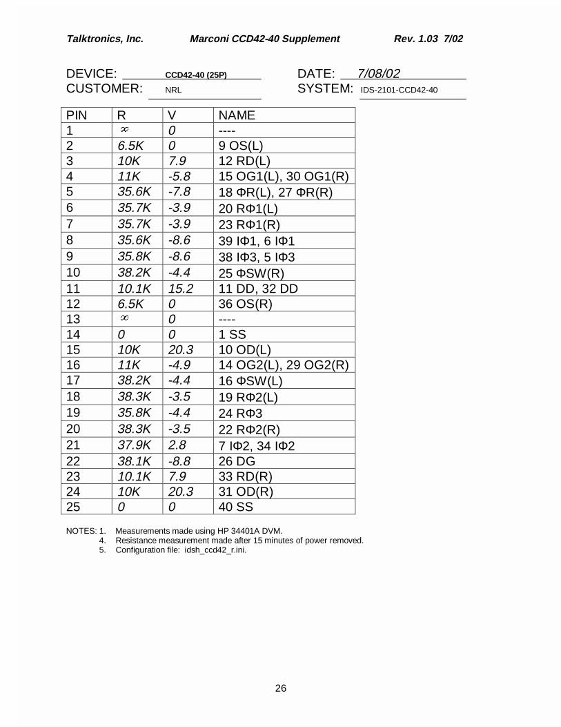
DEVICE: CCD42-40 (25P) DATE: 7/08/02CUSTOMER: NRL SYSTEM: IDS-2101-CCD42-40
PIN R V NAME1 � 0 ----2 6.5K 0 9 OS(L)3 10K 7.9 12 RD(L)4 11K -5.8 15 OG1(L), 30 OG1(R)5 35.6K -7.8 18 ΦR(L), 27 ΦR(R)6 35.7K -3.9 20 RΦ1(L)7 35.7K -3.9 23 RΦ1(R)8 35.6K -8.6 39 IΦ1, 6 IΦ19 35.8K -8.6 38 IΦ3, 5 IΦ310 38.2K -4.4 25 ΦSW(R)11 10.1K 15.2 11 DD, 32 DD12 6.5K 0 36 OS(R)13 � 0 ----14 0 0 1 SS15 10K 20.3 10 OD(L)16 11K -4.9 14 OG2(L), 29 OG2(R)17 38.2K -4.4 16 ΦSW(L)18 38.3K -3.5 19 RΦ2(L)19 35.8K -4.4 24 RΦ320 38.3K -3.5 22 RΦ2(R)21 37.9K 2.8 7 IΦ2, 34 IΦ222 38.1K -8.8 26 DG23 10.1K 7.9 33 RD(R)24 10K 20.3 31 OD(R)25 0 0 40 SS
NOTES: 1. Measurements made using HP 34401A DVM.4. Resistance measurement made after 15 minutes of power removed.5. Configuration file: idsh_ccd42_r.ini.

Talktronics, Inc. Marconi CCD42-40 Supplement Rev. 1.03 7/02
27
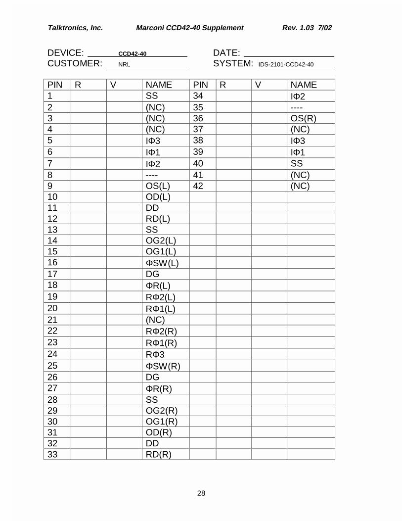
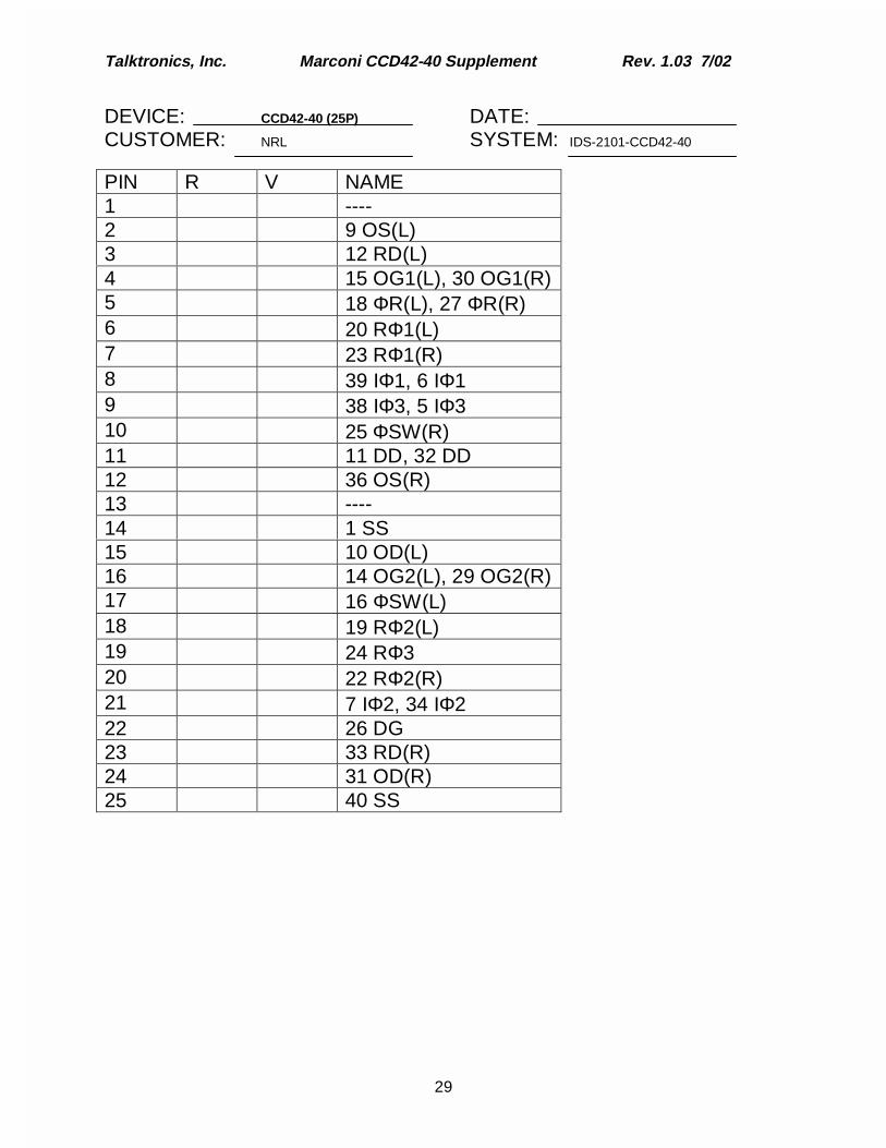
DEVICE SOCKET TEST FORMS
The following pages contain blank test forms that can be used during system checkout,and should be used whenever changes are made to the system hardware, timing orvoltages, that might affect the CCD. It is a good procedure to verify pin voltages andimpedances with the CCD removed whenever any questionable or substantial changesare made to setup.
Talktronics, Inc. Marconi CCD42-40 Supplement Rev. 1.03 7/02
28
DEVICE: CCD42-40 DATE:CUSTOMER: NRL SYSTEM: IDS-2101-CCD42-40
PIN R V NAME PIN R V NAME1 SS 34 IΦ22 (NC) 35 ----3 (NC) 36 OS(R)4 (NC) 37 (NC)5 IΦ3 38 IΦ36 IΦ1 39 IΦ17 IΦ2 40 SS8 ---- 41 (NC)9 OS(L) 42 (NC)10 OD(L)11 DD12 RD(L)13 SS14 OG2(L)15 OG1(L)16 ΦSW(L)17 DG18 ΦR(L)19 RΦ2(L)20 RΦ1(L)21 (NC)22 RΦ2(R)23 RΦ1(R)24 RΦ325 ΦSW(R)26 DG27 ΦR(R)28 SS29 OG2(R)30 OG1(R)31 OD(R)32 DD33 RD(R)
Talktronics, Inc. Marconi CCD42-40 Supplement Rev. 1.03 7/02
29
DEVICE: CCD42-40 (25P) DATE:CUSTOMER: NRL SYSTEM: IDS-2101-CCD42-40
PIN R V NAME1 ----2 9 OS(L)3 12 RD(L)4 15 OG1(L), 30 OG1(R)5 18 ΦR(L), 27 ΦR(R)6 20 RΦ1(L)7 23 RΦ1(R)8 39 IΦ1, 6 IΦ19 38 IΦ3, 5 IΦ310 25 ΦSW(R)11 11 DD, 32 DD12 36 OS(R)13 ----14 1 SS15 10 OD(L)16 14 OG2(L), 29 OG2(R)17 16 ΦSW(L)18 19 RΦ2(L)19 24 RΦ320 22 RΦ2(R)21 7 IΦ2, 34 IΦ222 26 DG23 33 RD(R)24 31 OD(R)25 40 SS

Talktronics, Inc. Marconi CCD42-40 Supplement Rev. 1.03 7/02
30
NOTES:

Talktronics, Inc. Marconi CCD42-40 Supplement Rev. 1.03 7/02
31

Talktronics, Inc. Marconi CCD42-40 Supplement Rev. 1.03 7/02
32
Talktronics, Inc. Marconi CCD42-40 Supplement Rev. 1.03 7/02
33
-- END --