Embed Size (px)
Citation preview
Taikan Suehara, AWLC14@FNAL, 13 May 2014 page 1
Status of SiW-ECAL Status of SiW-ECAL development for ILDdevelopment for ILD
Taikan Suehara(Kyushu University)
on behalf of ILD SiW-ECAL development group
Taikan Suehara, AWLC14@FNAL, 13 May 2014 page 2
ILD Silicon-ECAL developmentILD Silicon-ECAL development
Taikan Suehara, AWLC14@FNAL, 13 May 2014 page 3
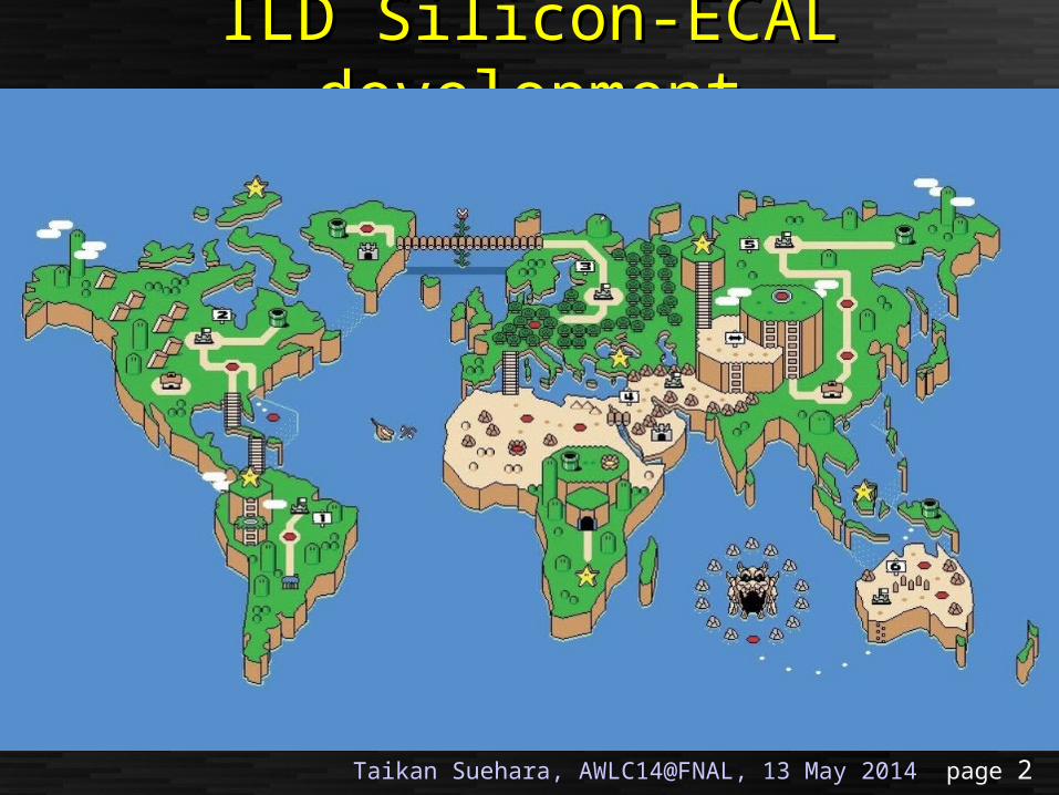
ILD Silicon-ECAL developmentILD Silicon-ECAL development
FranceLLR, LAL, LPNHE, LPSC Japan
Kyushu, Tokyo
Taikan Suehara, AWLC14@FNAL, 13 May 2014 page 4
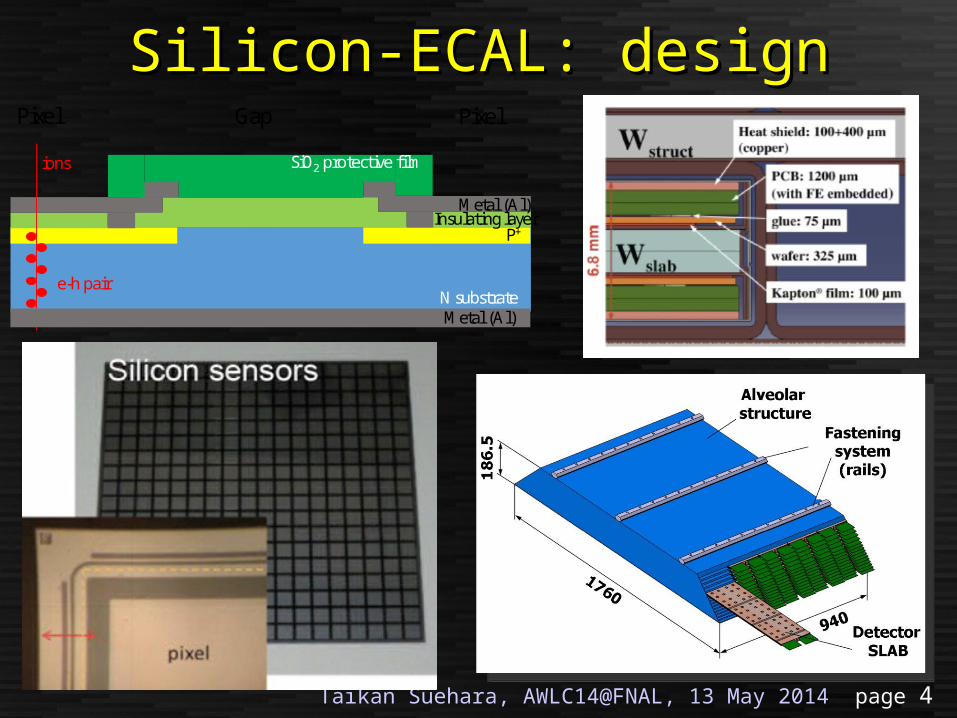
Silicon-ECAL: designSilicon-ECAL: design
N substrate
P+
Metal (Al)Insulating layer
SiO2 protective film
e-h pair
Metal (Al)
ions
PixelGapPixel
Taikan Suehara, AWLC14@FNAL, 13 May 2014 page 5
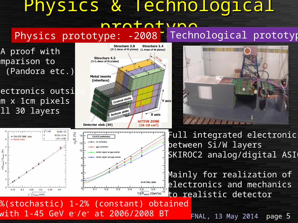
Physics & Technological Physics & Technological prototypeprototype
16.5%(stochastic) 1-2% (constant) obtainedwith 1-45 GeV e-/e+ at 2006/2008 BT
Physics prototype: -2008
PFA proof withcomparison toMC (Pandora etc.)
electronics outside1cm x 1cm pixelsfull 30 layers
Technological prototype
Full integrated electronicsbetween Si/W layersSKIROC2 analog/digital ASICs
Mainly for realization ofelectronics and mechanicsto realistic detector

Taikan Suehara, AWLC14@FNAL, 13 May 2014 page 6
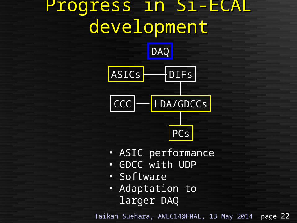
Progress in Si-ECAL Progress in Si-ECAL developmentdevelopment
Mechanics
• PCB production(BGA/CIB)
• Gluing• Assembly• Cooling
DAQ
ASICs DIFs
LDA/GDCCsCCC
PCs
• Guard rings• Doping
Sensor design
• ASIC performance• GDCC with UDP• Software• Adaptation to
larger DAQ
• Overall size• Layers• Hybrid
Optimization
Taikan Suehara, AWLC14@FNAL, 13 May 2014 page 7
Progress in Si-ECAL Progress in Si-ECAL developmentdevelopment
• Guard rings• Doping
Sensor design
Taikan Suehara, AWLC14@FNAL, 13 May 2014 page 8
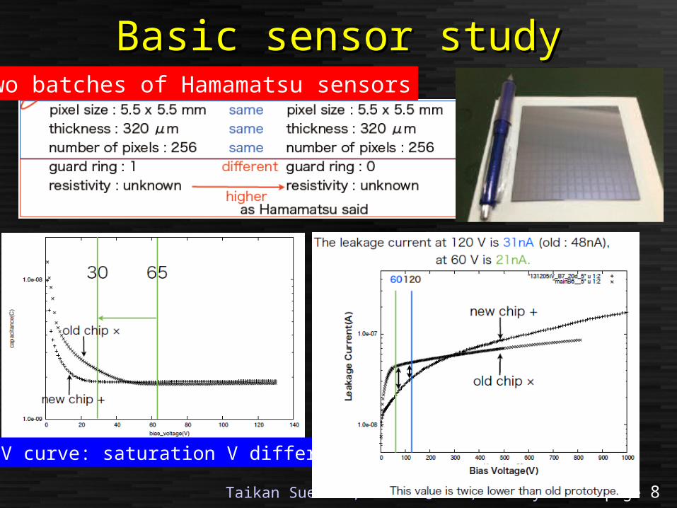
Basic sensor studyBasic sensor studyTwo batches of Hamamatsu sensors
C-V curve: saturation V differs
Taikan Suehara, AWLC14@FNAL, 13 May 2014 page 9
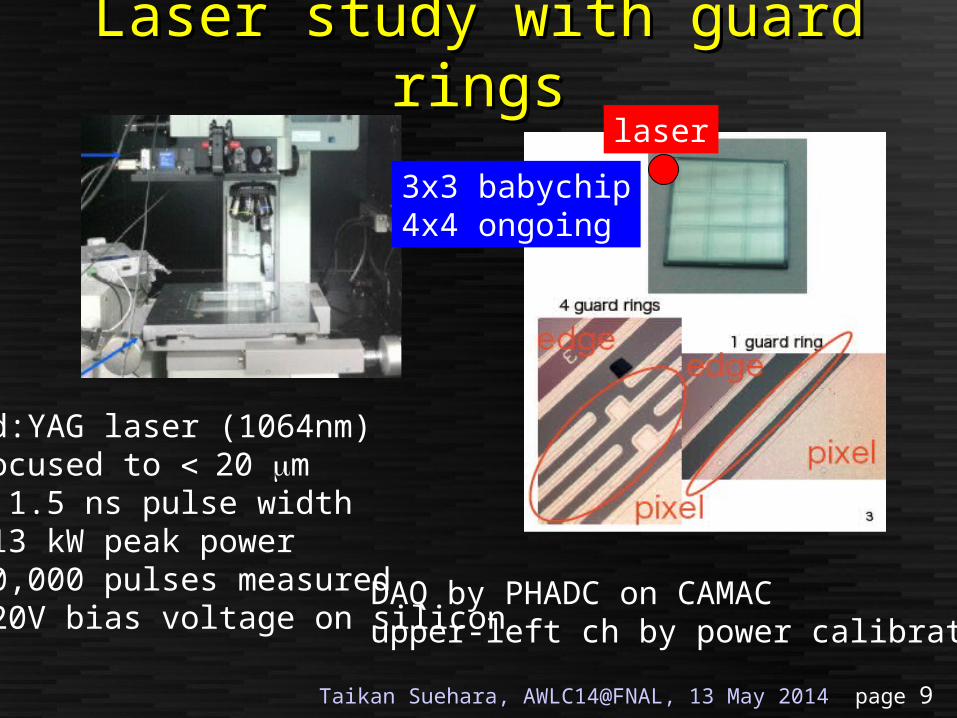
Laser study with guardLaser study with guard ringsrings
3x3 babychip4x4 ongoing
laser
Nd:YAG laser (1064nm)focused to 20 m~ 1.5 ns pulse width~13 kW peak power10,000 pulses measured120V bias voltage on silicon
DAQ by PHADC on CAMACupper-left ch by power calibration
Taikan Suehara, AWLC14@FNAL, 13 May 2014 page 10
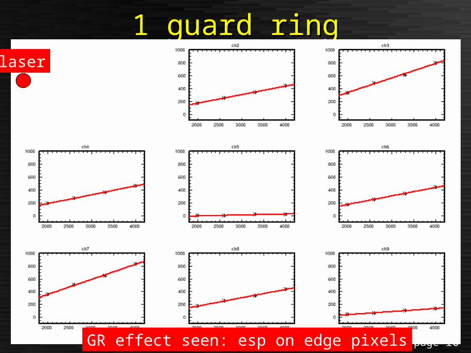
1 guard ring1 guard ringlaser
GR effect seen: esp on edge pixels
Taikan Suehara, AWLC14@FNAL, 13 May 2014 page 11
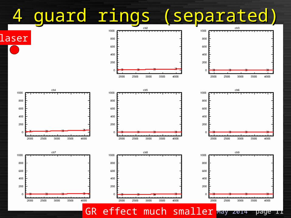
4 guard rings (separated)4 guard rings (separated)laser
GR effect much smaller
Taikan Suehara, AWLC14@FNAL, 13 May 2014 page 12
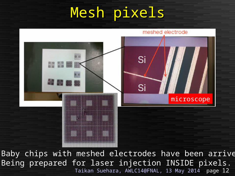
Mesh pixelsMesh pixels
microscope
Baby chips with meshed electrodes have been arrived.Being prepared for laser injection INSIDE pixels.
Taikan Suehara, AWLC14@FNAL, 13 May 2014 page 13
Progress in Si-ECAL Progress in Si-ECAL developmentdevelopment
Mechanics
• PCB production(BGA/CIB)
• Gluing• Assembly• Cooling
Taikan Suehara, AWLC14@FNAL, 13 May 2014 page 14
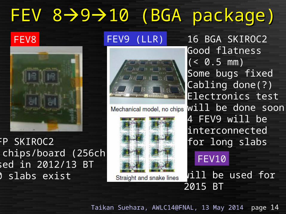
FEV 8FEV 89910 (BGA package)10 (BGA package)FEV8
QFP SKIROC24 chips/board (256ch)used in 2012/13 BT10 slabs exist
FEV9 (LLR) 16 BGA SKIROC2Good flatness(< 0.5 mm)Some bugs fixedCabling done(?)Electronics testwill be done soon4 FEV9 will beinterconnectedfor long slabs
FEV10
will be used for2015 BT
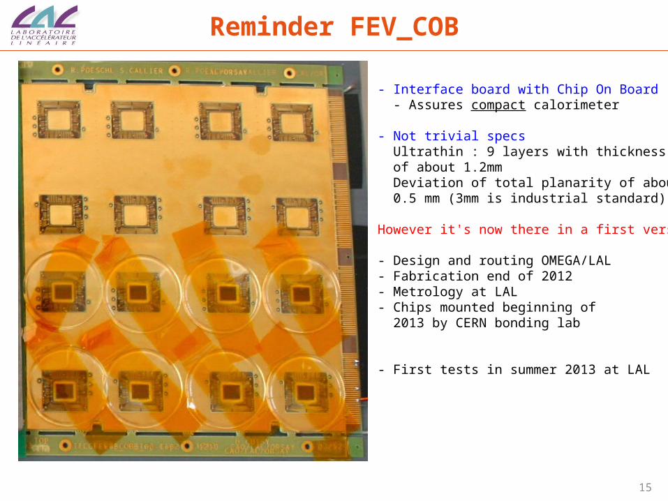
Reminder FEV_COB
15
- Interface board with Chip On Board - Assures compact calorimeter - Not trivial specs Ultrathin : 9 layers with thickness of about 1.2mm Deviation of total planarity of about 0.5 mm (3mm is industrial standard)
However it's now there in a first version
- Design and routing OMEGA/LAL- Fabrication end of 2012 - Metrology at LAL- Chips mounted beginning of 2013 by CERN bonding lab
- First tests in summer 2013 at LAL

Cooperation with EOS
16
- Korean company EOS has declared to be ready to produce the PCB -> Relaxed constraints on the thickness 1.2mm -> 1.5mm
- Technical discussion ongoing via mail but production is imminent
- Plans to assure entire PCB assembly in Korea - PCB production - ASIC bonding - Encapsulation
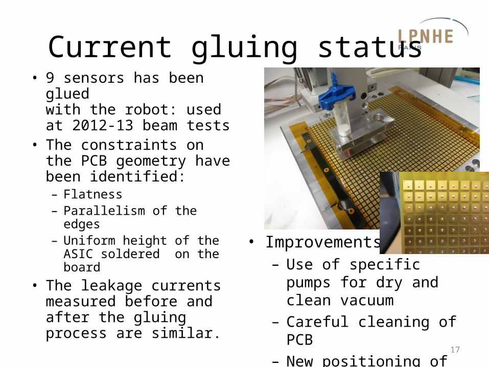
Current gluing status • 9 sensors has been glued
with the robot: usedat 2012-13 beam tests
• The constraints on the PCB geometry have been identified:– Flatness – Parallelism of the edges– Uniform height of the ASIC
soldered on the board• The leakage currents
measured before and after the gluing process are similar.
17
• Improvements– Use of specific pumps for dry
and clean vacuum– Careful cleaning of PCB– New positioning of the glue
dots for the external pads , to avoid short-circuits.
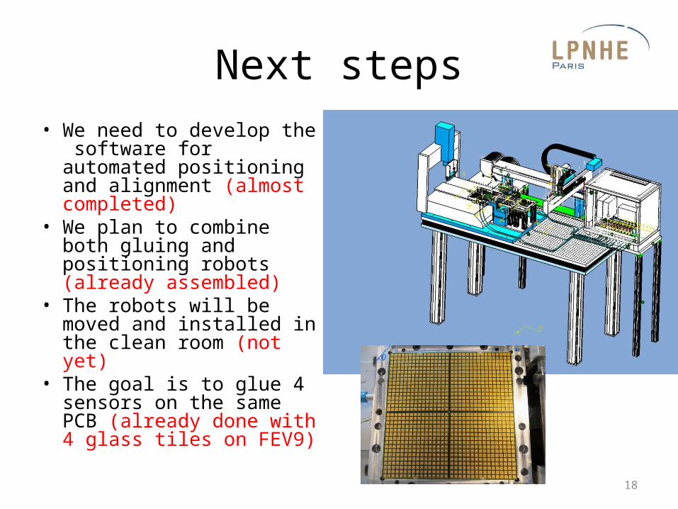
Next steps• We need to develop the
software for automated positioning and alignment (almost completed)
• We plan to combine both gluing and positioning robots (already assembled)
• The robots will be moved and installed in the clean room (not yet)
• The goal is to glue 4 sensors on the same PCB (already done with 4 glass tiles on FEV9)
18
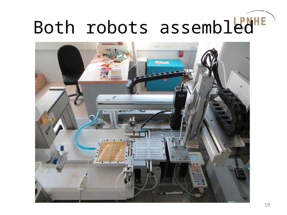
Both robots assembled
19
Taikan Suehara, AWLC14@FNAL, 13 May 2014 page 20
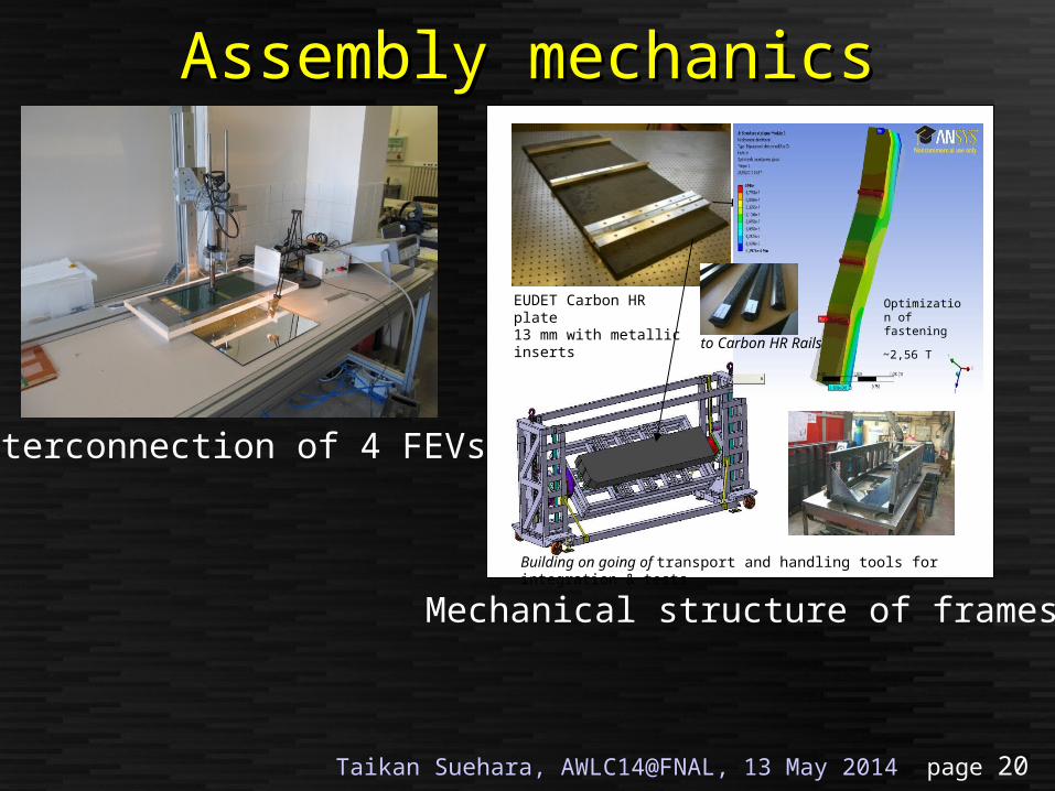
Assembly mechanicsAssembly mechanics
Interconnection of 4 FEVs
Building on going of transport and handling tools for integration & tests
~2,56 T
Optimization of fastening
to Carbon HR Rails
EUDET Carbon HR plate 13 mm with metallic inserts
Mechanical structure of frames
CALICE Collaboration Meeting March 2014
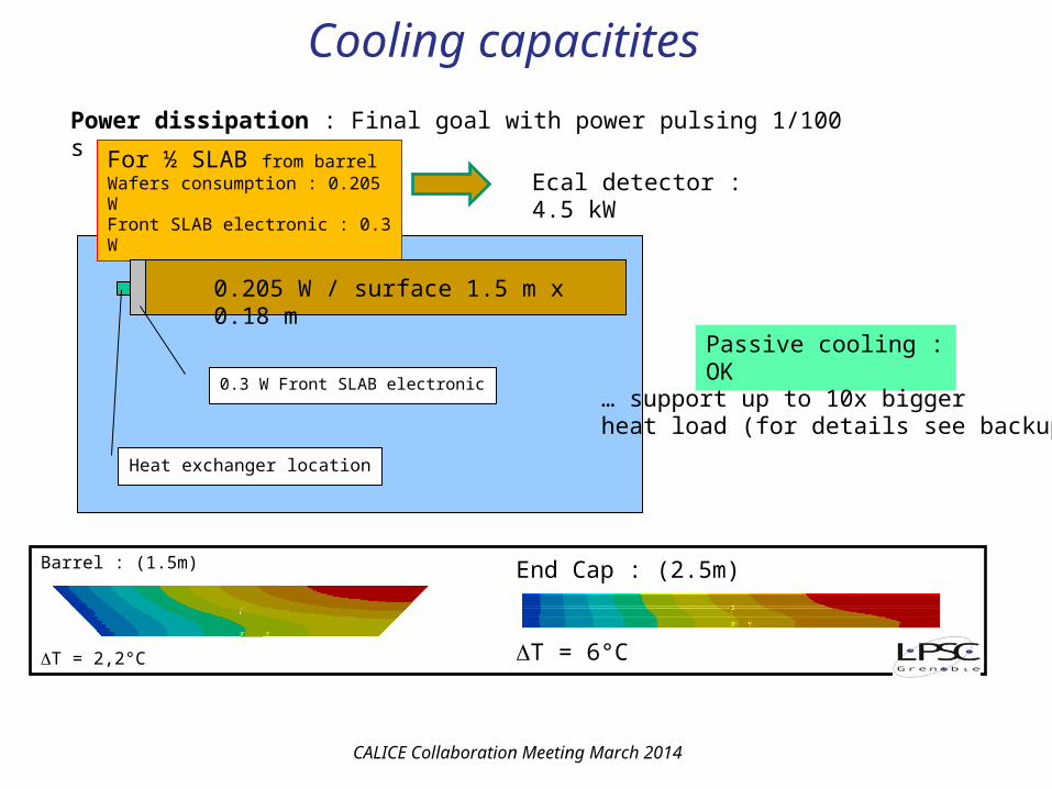
Power dissipation : Final goal with power pulsing 1/100 s
Barrel : (1.5m)
T = 2,2°C
For ½ SLAB from barrelWafers consumption : 0.205 WFront SLAB electronic : 0.3 W
Ecal detector : 4.5 kW
0.205 W / surface 1.5 m x 0.18 m
0.3 W Front SLAB electronic
Heat exchanger location
End Cap : (2.5m)
T = 6°C
Passive cooling : OK
Cooling capacitites
… support up to 10x biggerheat load (for details see backup)
Taikan Suehara, AWLC14@FNAL, 13 May 2014 page 22
Progress in Si-ECAL Progress in Si-ECAL developmentdevelopment
DAQ
ASICs DIFs
LDA/GDCCsCCC
PCs
• ASIC performance• GDCC with UDP• Software• Adaptation to
larger DAQ
Taikan Suehara, AWLC14@FNAL, 13 May 2014 page 23
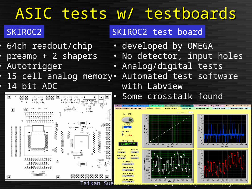
ASIC tests w/ testboardsASIC tests w/ testboardsSKIROC2
• 64ch readout/chip• preamp + 2 shapers• Autotrigger• 15 cell analog memory• 14 bit ADC
SKIROC2 test board
• developed by OMEGA• No detector, input holes• Analog/digital tests• Automated test software
with Labview• Some crosstalk found
Taikan Suehara, AWLC14@FNAL, 13 May 2014 page 24
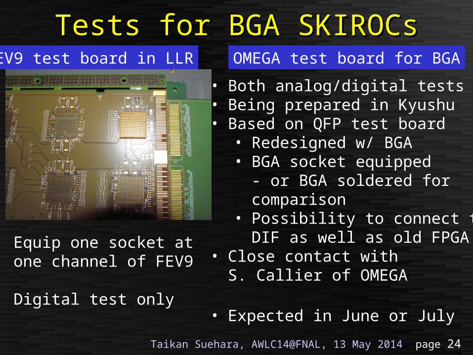
Tests for BGA SKIROCsTests for BGA SKIROCsFEV9 test board in LLR OMEGA test board for BGA
• Both analog/digital tests• Being prepared in Kyushu• Based on QFP test board
• Redesigned w/ BGA• BGA socket equipped
- or BGA soldered forcomparison
• Possibility to connect toDIF as well as old FPGA
• Close contact withS. Callier of OMEGA
• Expected in June or July
Equip one socket atone channel of FEV9
Digital test only
Taikan Suehara, AWLC14@FNAL, 13 May 2014 page 25
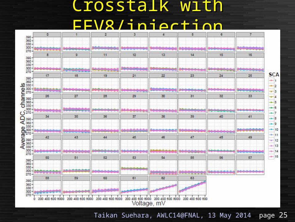
Crosstalk with FEV8/injectionCrosstalk with FEV8/injection
Taikan Suehara, AWLC14@FNAL, 13 May 2014 page 26
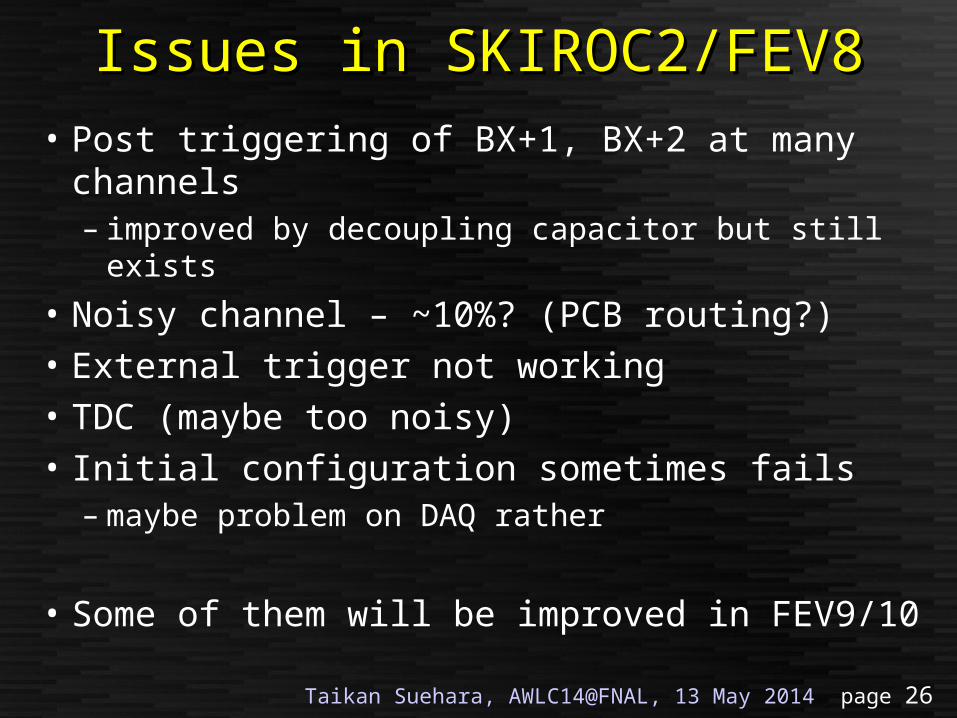
Issues in SKIROC2/FEV8Issues in SKIROC2/FEV8• Post triggering of BX+1, BX+2 at many
channels– improved by decoupling capacitor but still
exists
• Noisy channel – ~10%? (PCB routing?)• External trigger not working• TDC (maybe too noisy)• Initial configuration sometimes fails
– maybe problem on DAQ rather
• Some of them will be improved in FEV9/10
Taikan Suehara, AWLC14@FNAL, 13 May 2014 page 27
7 x DIFs HDMI
CCC HDMI
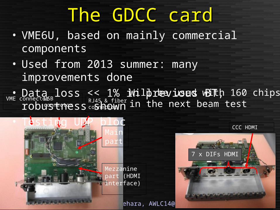
RJ45 & fiber connectorVME connectorUSB connector
Main part
Mezzanine part (HDMIinterface)
• VME6U, based on mainly commercial components
• Used from 2013 summer: many improvements done
• Data loss << 1% in previous BT, robustness shown
• Testing UDP bloc
The GDCC cardThe GDCC card
Will be used with 160 chipsin the next beam test
Taikan Suehara, AWLC14@FNAL, 13 May 2014 page 28
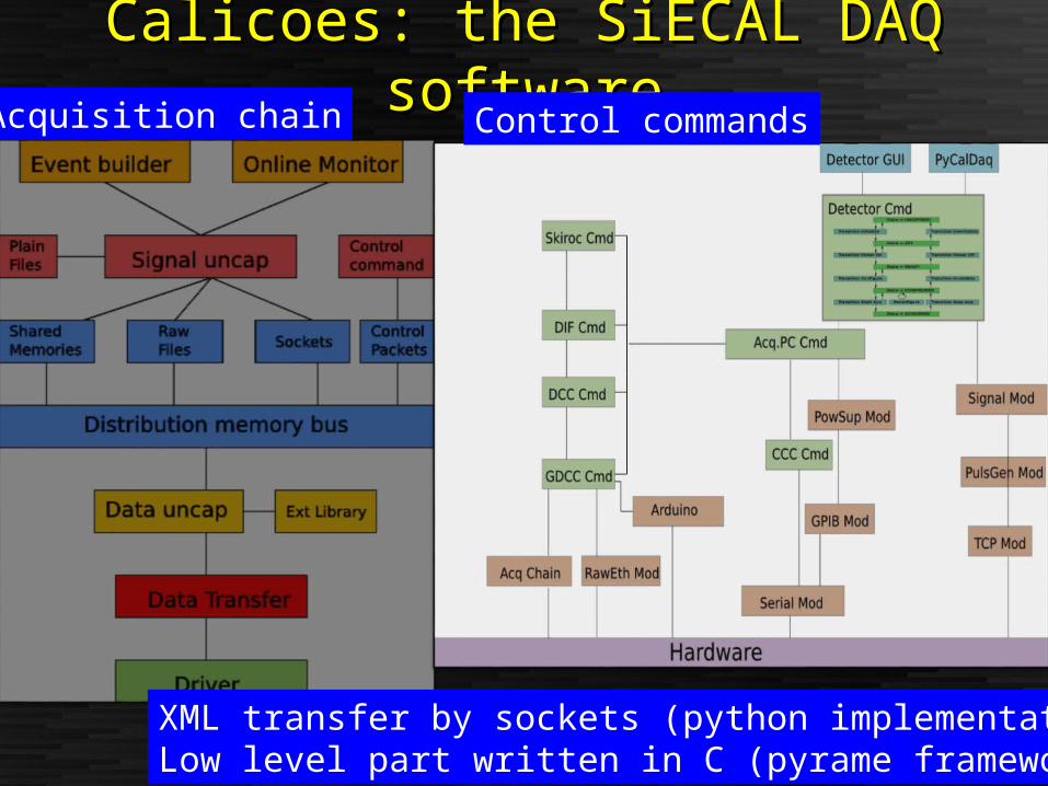
CalicoesCalicoes: the SiECAL DAQ software: the SiECAL DAQ softwareAcquisition chain Control commands
XML transfer by sockets (python implementation)Low level part written in C (pyrame framework)
Taikan Suehara, AWLC14@FNAL, 13 May 2014 page 29
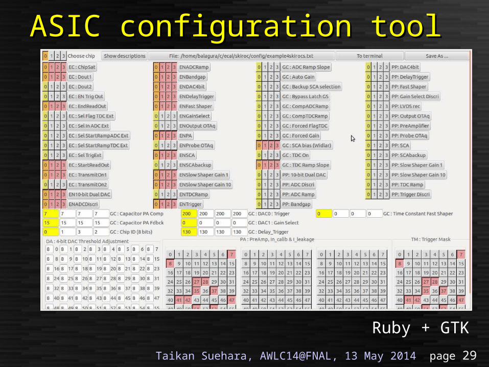
ASIC configuration tool ASIC configuration tool
Ruby + GTK
Taikan Suehara, AWLC14@FNAL, 13 May 2014 page 30
• We should integrate on larger DAQ systems for combined testbeam etc.
• We plan to use EUDAQ (as a first trial)• Also investigating Si/Sc combined DAQ
for hybrid ECAL– Or anyone else using ROC chips– Or more (trackers?) into real ILD?
• Hopefully come first in this summer
Efforts forEfforts for larger DAQ larger DAQ
Taikan Suehara, AWLC14@FNAL, 13 May 2014 page 31
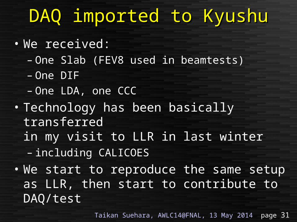
• We received:– One Slab (FEV8 used in beamtests)– One DIF– One LDA, one CCC
• Technology has been basically transferredin my visit to LLR in last winter– including CALICOES
• We start to reproduce the same setup as LLR, then start to contribute to DAQ/test
DAQ imported to KyushuDAQ imported to Kyushu
Taikan Suehara, AWLC14@FNAL, 13 May 2014 page 32
Progress in Si-ECAL Progress in Si-ECAL developmentdevelopment
• Overall size• Layers• Hybrid
Optimization
Taikan Suehara, AWLC14@FNAL, 13 May 2014 page 33
Optimization with PFAOptimization with PFA
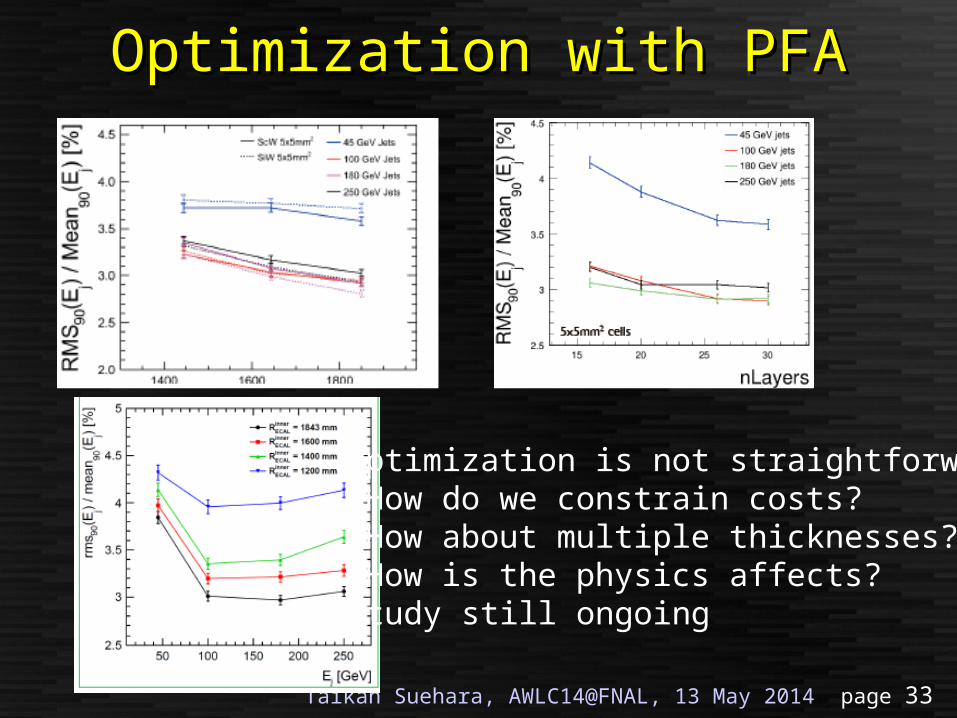
Optimization is not straightforward•How do we constrain costs?•How about multiple thicknesses?•How is the physics affects?Study still ongoing
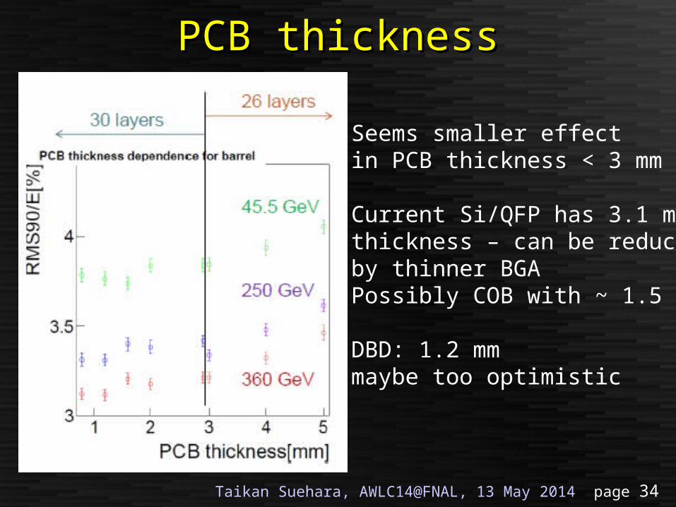
Taikan Suehara, AWLC14@FNAL, 13 May 2014 page 34
PCB thicknessPCB thickness
Seems smaller effectin PCB thickness < 3 mm
Current Si/QFP has 3.1 mmthickness – can be reducedby thinner BGAPossibly COB with ~ 1.5 mm
DBD: 1.2 mmmaybe too optimistic
Taikan Suehara, AWLC14@FNAL, 13 May 2014 page 35
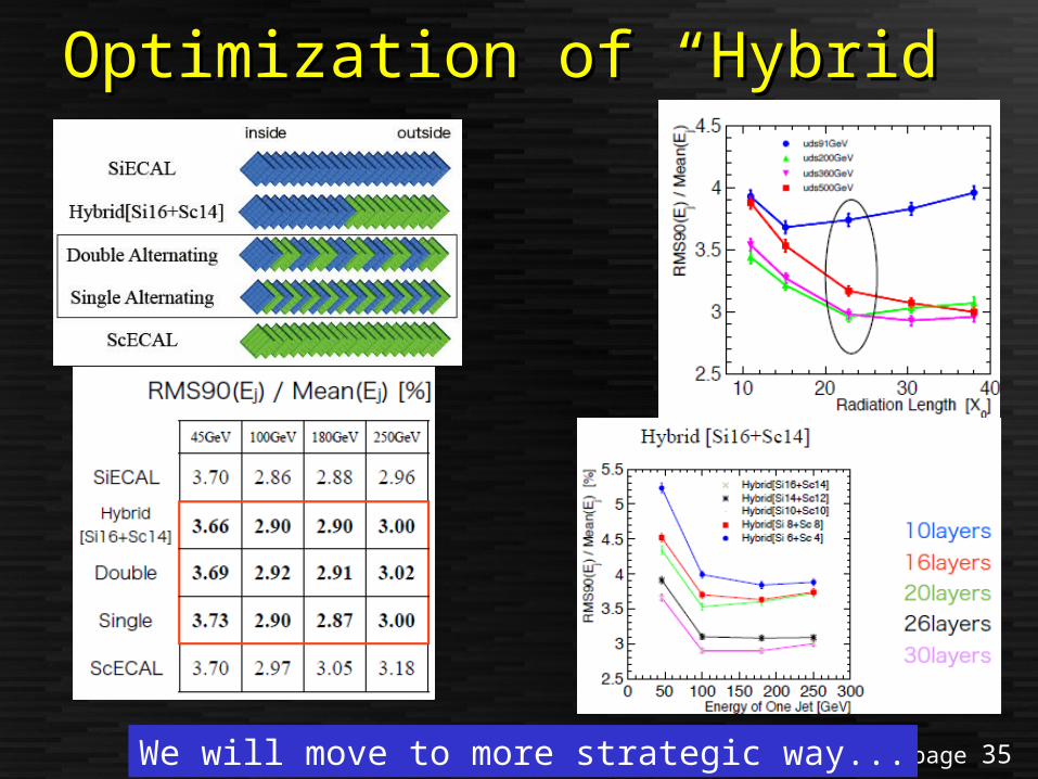
Optimization of “Hybrid”Optimization of “Hybrid”
We will move to more strategic way...
Taikan Suehara, AWLC14@FNAL, 13 May 2014 page 36
• We will finalize the optimization– Of sensors– Of geometries (with physics motivation)
• We will prepare for the next BT in 2015– With FEV10/GDCC/software– With bigger scale of production
• We will prepare for the mass production– Automated test/assembly etc.– More consideration on mechanics
• We will widen the collaboration/cooperation
SummarySummary