Embed Size (px)
Citation preview

1
Table&of&content&
&ESREF 2015 Editorial ....................................................................................................................... 3!ESREF 2015 Committees ................................................................................................................ 4!
Steering Committee ...................................................................................................................... 4!Organizing Committee .................................................................................................................. 5!Technical Program Committee ..................................................................................................... 6!Event Committee ........................................................................................................................ 10!
ESREF 2015 Invited Papers ........................................................................................................... 11!Keynote talks .............................................................................................................................. 11!Sister conference exchange papers ........................................................................................... 12!Invited papers in topical sessions ............................................................................................... 13!
ESREF 2015 Tutorials .................................................................................................................... 19!ESREF 2015 Workshops ................................................................................................................ 25!
Chip level Advanced Failure Analysis case studies .................................................................... 25!Student Research Speed Dating ................................................................................................ 25!Modeling the reliability at system level : tools and methodology ................................................ 26!Advanced tools and techniques flash presentations ................................................................... 26!
Methods and tools for Failure Analysis and Reliability ..................................................... 26!Fault isolation - defect localization ...................................................................................... 27!Sample Prep ........................................................................................................................... 27!Non Destructive Testing and Physical Characterization ................................................... 28!Nanoscale electrical measurement ..................................................................................... 29!
OEMs for components providers ................................................................................................ 29!DSM Technology impact on safety assessment ......................................................................... 30!Failure Analysis of Critical Systems ........................................................................................... 30!European FIB Users Group workshop ........................................................................................ 30!Reliability of avionics power electronics ...................................................................................... 31!Design and test for robustness and reliability ............................................................................. 31!
Design for reliability (PCB, subsystem level) ........................................................................... 32!Statistical Analysis of Big Test Data ........................................................................................ 32!Radiation testing on electronic devices ................................................................................... 33!
ESREF 2015 program .................................................................................................................... 34!Monday, October 5, 2015 ........................................................................................................... 35!Tuesday, October 6, 2015 .......................................................................................................... 37!

2
Wednesday, October 7, 2015 ..................................................................................................... 43!Thursday, October 8, 2015 ......................................................................................................... 49!Friday, October 9, 2015 .............................................................................................................. 54!
ESREF 2015 Paper Abstracts ........................................................................................................ 56!SESSION A: Quality and Reliability Assessment - Techniques and Methods for Devices and Systems ...................................................................................................................................... 56!SESSION B1: Si-Technologies & Nanoelectronics: Hot carriers, high K, gate materials ........... 59!SESSION B3: Si-Technologies & Nanoelectronics: ESD, Latch-up, Radiation Effects .............. 61!SESSION C: Failure Analysis ..................................................................................................... 63!SESSION D1: Microwave & Power Wide Band-Gap SC Devices .............................................. 66!SESSION D2: Photonic .............................................................................................................. 68!SESSION D3: Photovoltaic & Organic Devices .......................................................................... 70!SESSION E1: Packaging & Assembly ........................................................................................ 71!SESSION E2: MEMS, MOEMS, NEMS & Nano-objects ............................................................ 73!SESSION F: Power devices ....................................................................................................... 74!SESSION G: Space, Aeronautic & Embedded Systems ............................................................ 78!SESSION H: European FIB User Group (EFUG) ....................................................................... 80!ESREF 2015 Build your own ESREF 2015 ................................................................................ 81!
ESREF 2015 Lab Tours ................................................................................................................. 82!LAAS Lab tour ............................................................................................................................. 82!ITEC-Lab ..................................................................................................................................... 82!TRAD Industry tour ..................................................................................................................... 84!
ESREF 2015 Industrial Sponsors ................................................................................................... 85!ESREF 2015 Exhibition .................................................................................................................. 88!
ESREF 2015 Exhibiting Companies description ......................................................................... 88!Exhibition layout .......................................................................................................................... 96!
ESREF 2015 Practical Information ................................................................................................. 97!Toulouse, the Pink City ............................................................................................................... 97!Public transportation ................................................................................................................... 97!Mobile application ....................................................................................................................... 97!

3
ESREF 2015 Editorial Welcome to the 26th European Symposium on Reliability of Electron Devices, Failure Physics and Analysis, ESREF 2015, at Toulouse (France) from October 5th to October 9th, 2015.
This international symposium continues to focus on recent developments and future directions in Quality and Reliability Management of materials, devices and circuits for micro-, nano-, and optoelectronics. It provides a European forum for developing all aspects of reliability management and innovative analysis techniques for present and future electronic applications.
For its first time in Toulouse - world center for aeronautics with Airbus assembly line, European capital of the space industry and number 1 in France for embedded electronic systems - specific topics are dedicated to these applications involving severe environment and harsh reliability challenges in addition to the core topics of the conference.
The Technical Program of ESREF 2015 has been defined by the Technical Program Committee (TPC) organized in thirteen sub-committees with more than 250 renowned experts in the field of reliability of electronic components and systems. The TPC has proceeded to a careful selection from 252 extended summaries and selected 103 papers to be presented during the oral sessions and 62 as posters. This conference would not be possible without the commitment and expertise of all these contributors.
Our main focus in 2015 is space, aeronautics and embedded systems. Two keynote speeches – one related to Mars exploration reliability challenges and the other on hardware cybersecurity – will open the conference on Monday, October 5. Over the three next days, the conference is organized in four parallel topical tracks composed of tutorials, invited presentation, session and workshop. Nine invited speakers who are recognized experts in their fields will give an overview of the state-of-the-art and special focus on advanced research work.
Within the topical tracks, 8 tutorials are offered to allow attendees refreshing and expanding their knowledge.
Based on an exchange agreement with the committees of the International Symposium on the Physical & Failure Analysis of Integrated Circuits Conference (IPFA 2015), the International Reliability Physics Symposium (IRPS 2015) and the International Symposium for Testing and Failure Analysis (ISTFA 2014), authors of awarded papers have been invited to present their work at ESREF 2015. These exchanges prove the fruitful collaboration between the Committees of these three conferences.
10 Workshops organized in correlation with the ESREF conference will give the opportunity to exchange the know-how and field returns on specific topics and in particular, in relationship with aeronautics, space and embedded systems.
Exhibition with state-of-the-art equipment starts on Monday afternoon and will host coffee breaks, lunches, poster sessions and author’s corner to maximize interaction between attendees and exhibitors.
Finally, we would like to warmly thank all our sponsors that allowed setting up this exciting and high-quality program:
the IEEE Electron Devices Society for its technical co-sponsorship. the Centre National de la Recherche Scientifique (CNRS), the University of Toulouse III – Paul Sabatier, the Centre National d’Etudes Spatiales (CNES) SO Toulouse Convention Bureau and our industrial sponsors:
Gold sponsor: Sector Technologies Silver sponsors: THALES Group and Hamamatsu, Bronze sponsors: Digit Concept, FEI, Intraspec Technologies, Kleindiek nanotechnik, Orsay Physics, Raith GmbH. All the members of the Program and of the Technical Committees, all the reviewers and the Corresponding Members deserve our congratulations and our thanks for their involvement and their efforts to make ESREF meet the requirements of an international event dedicated to Quality and Reliability of Electron Devices.
We are very happy to meet you in TOULOUSE for a memorable experience.
Marise BAFLEUR Philippe PERDU .
ESREF 2015 Chair ESREF 2015 Vice-Chair

4
ESREF 2015 Committees
Steering Committee
Alain BENSOUSSAN IRT Saint Exupéry / Thales Alenia Space(France) Jaap BISSCHOP NXP Semiconductors (The Netherlands) Christian BOIT TUB - Tech. University of Berlin (Germany) Giovanni BUSATTO University of Cassino (Italy) Mauro CIAPPA ETH Zürich (Switzerland) Yves DANTO IMS, University of Bordeaux (France) Ingrid De WOLF IMEC (Belgium) Gert ERIKSEN GRUNDFOS (Denmark) Fausto FANTINI University of Modena (Italy) Bruno FOUCHER AIRBUS GROUP INNOVATION (France) Philippe GALY STMicroelectronics (France) Wolfgang GERLING ECPE (Germany) Siegfried GOERLICH Infineon (Germany) Ralf HEIDERHOFF University of Wuppertal (Germany) Nathalie LABAT IMS, University of Bordeaux (France) Jim R. LLOYD University of Albany (USA) Gaudenzio MENEGHESSO University of Padova (Italy) Enrique MIRANDA University Autonoma Barcelona (Spain) Jean-Luc MURARO THALES Alenia Space (France) George PAPAIOANNOU University of Athens (Greece) Philippe PERDU CNES (France) Cora SALM University of Twente (The Netherlands) Ninoslav STOJADINOVIC University of Nis (Serbia) André TOUBOUL IMS, University of Bordeaux (France) Massimo VANZI University of Cagliari (Italy) Eckhard WOLFGANG ECPE (Germany) Wolfgang WONDRAK Daimler Chrysler (Germany)

5
Organizing Committee
Conference Chair & Vice-Chair Marise BAFLEUR LAAS-CNRS (France) Philippe PERDU CNES (France) Technical Program Chairs Hélène FREMONT IMS, University of Bordeaux (France) François MARC IMS, University of Bordeaux (France) Conference Scientific Support Christian BOIT TU Berlin (Germany) Fausto FANTINI University of Modena (Italy) Industrial Exhibition Jan GAUDESTAD NEOCERA (USA) Brigitte DUCROCQ LAAS-CNRS (France) Tutorial chair Peter JACOB EMPA (Switzerland) Giovanni BUSATTO University of Cassino (Italy) Workshop chairs Mauro CIAPPA ETH Zürich (Switzerland) Thomas ZIRILLI Freescale (France) Fulvio INFANTE Intraspec Technologies (France) Best Paper Award chair Matthias PETZOLD Fraunhofer-Institute for Mechanics of Materials (Germany) Best Poster Award chair David TRÉMOUILLES LAAS-CNRS (France) Audio/Video chairs Nicolas MAURAN LAAS-CNRS (France) Nicolas NOLHIER LAAS-CNRS (France) Organization Secretariat Ascension DE SOUSA BERDAT LAAS-CNRS (France) Event Committee chairs Alain BENSOUSSAN IRT Saint-Exupéry (France) André DURIER IRT Saint-Exupéry (France) Publicity Chairs Jérome TOUZEL INFINEON (Germany) Enrique MIRANDA University Autonoma Barcelona (Spain) Microelectronics Reliability Journal Edition Chairs Marise BAFLEUR LAAS-CNRS (France) Philippe PERDU CNES (France) Nicolas NOLHIER LAAS-CNRS (France) Hélène FREMONT IMS, University of Bordeaux (France) François MARC IMS, University of Bordeaux (France) ESREF Scientific support in TURKEY Ilknur BAYLAKOĞLU SATURN Consulting (Turkey) Webmaster David TRÉMOUILLES LAAS-CNRS (France)

6
Technical Program Committee Chairs: Hélène FREMONT, IMS, University Bordeaux (France) – François MARC, IMS, University Bordeaux (France) Quality and Reliability Assessment – Chairs: Ninoslav D. STOJADINOVIC, University of Nis (Serbia) - Bruno FOUCHER, AIRBUS GROUP INNOVATIONS (France) Christelle AUPETIT-BERTHELEMOT, ENSIL –University of Limoges (France) Olivia BLUDER, Kompetenzzentrum für Automobil- und Industrieelektronik GmbH – (Austria) Yves DANTO, IMS, University of Bordeaux (France) Vojkan DAVIDOVIC, University of NIS (Serbia) Milan JEVTIC, Institute of Physics (Serbia) Dimitrios KOUVATSOS, Institute NCSR "Demokritos" (Greece) Andreas MIDDENDORF, TU Berlin / Fraunhofer IZM (Germany)
Florian MOLIERE, Airbus Group Innovations (France) Lirida NAVINER, TELECOM ParisTech (France) Alexander NIKIFOROV, National Research Nuclear University "MEPHI" (Russia) Albena PASKALEVA, Bulgarian Academy of sciences (Bulgaria) M.K. RADHAKRISHNAN, Nanorel (India) Didier REGIS, THALES GROUP (France) Cora SALM, MESA+ Research Institute/ University of Twente (The Netherlands)
Si Technologies & Nanoelectronics: Hot carriers, high K, gate materials – Chairs: Alain BRAVAIX, ISEN (France) - Jim STATHIS, IBM Research (USA) Xavier AYMERICH, Univ. Autonoma Barcelona (Spain) Jean COIGNUS, CEA-LETI (France) Rainer DUSCHL, Infineon Technologies (Germany) Gabriella GHIDINI, STMicroelectronics (France) Dimitrios KOUVATSOS, Institute NCSR "Demokritos" (Greece) Paolo PAVAN, Università di Modena e Reggio Emilia (Italy)
Nagarajan RAGHAVAN, Singapore University of Technology and Design (Singapore) Rosana RODRIGUEZ, Universitat Autonoma de Barcelona (Spain) Cora SALM, MESA+ Research Institute/ University of Twente (The Netherlands)
Si Technologies & Nanoelectronics: Low K, Cu Interconnects – Chairs: Hervé JAOUEN, STMicroelectronics (France) - Eckhard LANGER, Globalfoundries (USA) Lucile ARNAUD, CEA Leti (France) Oliver AUBEL, Globalfoundries (Germany) Fen CHEN, IBM (USA) Cathryn J CHRISTIANSEN, IBM (USA) Kristof CROES, IMEC (Belgium) Vincent DWYER, Loughbourough University (UK) Xavier FEDERSPIEL, STMicroelectronics (France)
Martin GALL, Fraunhofer IKTS-MD (Germany) Chee Lip GAN, Nanyang Technological University (Singapore) Howard GAN, SMIC (China) Andrea PADOVANI, University of Modena (Italy) Xin-Ping QU, Fudan University (China) Frank SCHLAPHOF, Globalfoundries (Germany)
Si Technologies & Nanoelectronics: ESD, Latch-up, Radiation Effects – Chairs: Fabrice CAIGNET, LAAS-CNRS (France) - Philippe GALY, STMicroelectronics (France) - Vesselin VASSILEV, NOVORELL Technologies (USA) Bruno ALLARD, AMPERE- INSA Lyon (France) Patrice BESSE, Freescale Semiconductor (France) Gianluca BOSELLI, Texas Instruments ( USA) Lorenzo CERATI, STMicroelectronics (Italy) Denis FLANDRE, SST/EPL Ecole Polytechnique de Louvain (Belgium) Hörst GIESER, Fraunhofer IZM (Germany) Harald GOSSNER, Intel (Germany) Allesio GRIFFONI, OSRAM (Italy) Richard JANSEN, ESA (The Netherlands) Martin KERBER, Infineon (Germany) Paul LEROUX, KU Leuven (Belgium)
Martino LORENZINI, NXP (The Netherlands) Alessandro PACCAGNELLA, Università di Padova (Italy) Vincent POUGET, IES - Univ. Montpellier 2 (France) Christian RUSS, Intel Mobile Communications (Germany) Pascal SALOME, Serma Technologies (France) Adelina SHICKOVA, Infineon (Germany) Gerald SOELKNER, Infineon (Germany) Gerd VERMONT, ON Semiconductor (Belgium) Hei WONG, City University of Hong Kong (China) Beiping YANG, ASTRI (Hong Kong-China)

7
Failure Analysis – Chairs: Félix BEAUDOIN, GLOBALFOUNDRIES (USA) - Olivier CREPEL, AIRBUS GROUP INNOVATIONS (France) - Siegfried GOERLICH, INFINEON (Germany) - Ralf HEIDERHOFF, Bergische Universität Wuppertal (Germany) Abdellatif FIRITI, NXP (The Netherlands) Juergen GRUBER, ROOD MICROTEC (Germany) Stewart HOLLINGSHEAD, Texas Instruments (USA) Terence KANE, IBM (USA) Susane LI , SPANSION (USA) Ted LUNDQUIST, DCG Systems Wolfgang MERTIN, University Duisburg-Essen (Germany) Giovanna MURA, University of Cassino (Italy)
Koji NAKAMAE, IST Osaka (Japan) Vincent POUGET, IES (France) Antoine REVERDY, Sector Technologies (France) Jean-Philippe ROUX, Sector Technologies (France) Kevin SANCHEZ, CNES (France) Christian SCHMIDT, GlobalFoundries (USA) Zhigang SONG, IBM (USA) Ehrenfried ZSCHECH, Fraunhofer IZFP (Germany)
D1: Wide Band-Gap SC Devices – Chairs: Peter FRIEDRICHS, INFINEON (D) - Nathalie LABAT, IMS, University Bordeaux (France) - Gaudenzio MENEGHESSO, University of Padova (Italy) Andrew BARNES, ESA/ESTEC (The Netherlands) Michael DAMMAN, IAF Fraunhofer IAF (Germany) Dan FLEETWOOD, Vanderbilt University (USA) Tsuyoshi ISHIKAWA, Toyota Central R&D labs (Japan) Karine ISOIRD, LAAS-CNRS (France) Benoit LAMBERT, United Monolithic Semiconductors (France) Toshiide KIKKAWA, Transphorm Japan (Japan) Jan KUZMIK, Slovak Academy of Sciences (Slovakia)
Nathalie MALBERT, IMS, University Bordeaux (France) Denis MARCON, IMEC (Belgium) Roberto MENOZZI, University of Modena (Italy) Jean-Luc MURARO, Thales Alenia Space (France) Dionyz POGANY, TU WIEN (Austria) Michael UREN, University of Bristol (UK) Giovanni VERZELLESI, University of Modena (Italy) Joachim WÜRFL, Ferdinand-Braun-Institut (Germany)
D2: Photonic Devices – Chairs: Matteo MENEGHINI, University of Padova (Italy) - Massimo VANZI, University of Cagliari (Italy) Christelle AUPETIT-BERTHELEMOT, ENSIL –University of Limoges (France) Laurent BECHOU, IMS University Bordeaux (France) Alain BENSOUSSAN, IRT Saint-Exupéry (France) Daniel CASSIDY, University of McMaster Yannick DESHAYES, IMS University of Bordeaux (France) Alessio GRIFFONI, OSRAM (Italy)
Juan JIMENEZ, University of Valladolid (SP) Robert KAPLAR, SANDIA NATIONAL LABS (USA) Michel KRAKOWSKI, Thales 3-5 LAB (France) Laurent MENDIZABAL, CEA-LETI (France) Giovanna MURA, Univ. Cagliari (Italy) Tigran NSHANIAN, Philips Lumileds Lighting Co (The Netherlands) Osamu UEDA, Kanazawa University (Japan)
D3: Photovoltaic & Organic Devices – Chair: Nicola WRACHIEN, University of Padova (Italy) Andrea CESTER, University of Padova (Italy) Cosimo GERARDI, ST Microelectronics (Italy) Ralf HEIDERHOFF, University of Wuppertal (Germany) Morten MADSEN, University Of Southern Denmark (Denmark) Laurent MENDIZABAL, CEA-LETI (France)
Selina OLTHOF, Univ. Cologne (Germany) Andrea REALE, Università di Roma Tor Vergata (Italy) Thomas RIEDL, University of Wuppertal (Germany) Elisabeth VON HAUFF, Univ. Amsterdam (The Netherlands)

8
E1: Packaging & Assembly – Chairs: Geneviève DUCHAMP , IMS, University Bordeaux (France) -Kirsten WEIDE-ZAAGE, University of Hannover (Germany) Y. C CHAN, City University Hong Kong (China) Lorenzo CIANI, University of Florence (Italy) Alberto CORIGLIANO, Politecnico di Milano (Italy) Paolo COVA, Università di Parma (Italy) Yves DANTO, IMS, University of Bordeaux (France) Christian GAUTIER, Presto Engineering (France) Alexandrine GUEDON-GRACIA, IMS, University of Bordeaux (France) Xiao HU LIU, IBM TJ Watson Research Center (USA) Fulvio INFANTE, Intraspec Technologies (France) Yong LIU, Fairchild Semiconductor (USA)
Wilson MAIA, THALES R&T (France) Lutz MEINSHAUSEN, Washington State University (USA) Frédéric RICHARDEAU, LAPLACE-INPT (France) René RONGEN, NXP (The Netherlands) Vincent ROUGET, AIRBUS Group Innovations (France) Mohd Faizul bin Mohd SABRI, University of Malaya (Malaysia) Suhana Mohd SAID, University of Malaya (Malaysia) Marc WURZ, IMPT, University of Hannover (Germany)
E2: MEMS, MOEMS, NEMS & Nano-objects – Chairs: Fabio COCCETTI, elemca (France) - George PAPAIOANNOU, University of Athens (Greece) Elena BLOKHINA, University College Dublin (Ireland) Manuel DOMINGUEZ, Universitat Polytechnica Cataluna (Spain) David ELATA, Technion, Israel Institute of Technology (Israel) Evgeni GOUSEV, Qualcom Technologies Inc (USA)
Loukas MICHALAS, IMM – CNR (Italy) Patrick PONS, LAAS-CNRS (France) Bruno REIG, LETI – CEA (France) Herbert SHEA, EPFL (Switzerland) Jun-Bo YOON, KAIST (Korea)
F : POWER DEVICES – Chairs: Patrick TOUNSI, INSA, LAAS-CNRS (France) - Eckhard WOLFGANG, ECPE (Germany) Stéphane AZZOPARDI, IMS, Univ. Bordeaux (France) Reinhold BAYERER, Infineon (Germany) Philippe BENECH, IMEP-INPG (France) Frede BLAABJERG, Aalborg University (DK) Giovanni BREGLIO, University of Naples Federico II (Italy) Giovanni BUSATTO, University of Cassino (Italy) Alberto CASTELLAZZI, University of Nottingham (UK) Dinesh CHAMUND, Dynex Semiconductor (UK) Mauro CIAPPA, ETH Zurich (Switzerland) Chiara CORVASCE, ABB (Switzerland) Paolo COVA, University of Parma (Italy) Adeline FEYBESSE, FREESCALE (USA) Laurent GUILLOT, FREESCALE (France) Karsten GUTH, Infineon (Germany) Francesco IANUZZO, University of Cassino (Italy) Andrea IRACE, University of Naples Federico II (Italy) Nando KAMINSKI, University of Bremen (Germany) Kai KRIEGEL, Siemens (Germany) Stephane LEVEBVRE, CNAM (France)
Thomas LICHT, University of Applied Sciences in Düsseldorf (Germany) Josef LUTZ, TU Chemnitz (Germany) Régine MALLWITZ, TU Braunschweig (Germany) Michael NELHIEBEL, KAI Kompetenzzentrum Automobil- und Industrieelektronik (Germany) Ichiro OMURA, Kyushu Institute of Technology (Japan) Martin PFOST, Reutlingen University (Germany) Frédéric RICHARDEAU, LAPLACE-INPT (France) Uwe SCHEUERMANN, SEMIKRON (Germany) Hans-Joachim SCHULZE, Infineon (Germany) Norbert SELIGER, Rosenheim University of Applied Sciences (Germany) Dieter SILBER, University of Bremen (Germany) Hiroshi SUZUKI, HITACHI (Japan) Peter TUERKES, Infineon (Germany) Jean-Michel VINASSA, IMS, Univ. Bordeaux (France) Wolfgang WONDRAK, Daimler (Germany) Eric WOIRGARD, IMS, Univ. Bordeaux (France)

9
G: Space, Aeronautic & Embedded Systems – Chairs: Sonia BEN DHIA, LAAS-CNRS (France) - André DURIER, IRT Saint-Exupéry (France) - Florent MILLER, AIRBUS GROUP INNOVATIONS (France) - Fabian VARGAS, Catholic University - PUCRS (Brazil) Marcos Osmar AREND, AEL, Sistemas/Elbit Systems Ltd. (Brazil) İlknur BAYLAKOĞLU, SATURN Consulting – (Turkey) Eduardo BEZERRA, Federal University of Santa Catarina, Florianópolis (Brazil) Jerónimo BLOSTEIN, Centro Atómico - Instituo Balseiro, Bariloche (Argentina) Leticia Maria BOLZANI POEHLS, Catholic University - PUCRS, Porto Alegre (Brazil) Stéphanie BOURBOUSE, Airbus Defence and Space (France) Véronique FERLET CAVROIS, ESA (The Netherlands) David HELY, Grenoble Institute of Technology (France) Jean Claude LAPERCHE, Airbus Group (France) Dominique LENOIR, Renault (France) Fernanda LIMA KASTENSMIDT, Federal University of Rio Grande do Sul, Porto Alegre (Brazil)
José LIPOVETZKY, Centro Atómico - Instituo Balseiro, Bariloche (Argentina) Renaud MANGERET, Airbus Defence and Space (France) Francesca MARADEI, Sapienza de Rome (Italy) Maria MAZUREK, Airbus Group (France) Guy PEREZ, CNES (France) Mohamed RAMDANI, ESEO (France) Matteo SONZA REORDA, Politecnico di Torino, Torino (Italy) Régine SUTRA ORUS, IRT Saint-Exupéry-Zodiac (France) Daniel TRIAS, Serma Technologies (France) Damien VERDIER, Continental (France) Bertrand VRIGNON, Freescale Semiconductor (France)
H: European FIB User Group (EFUG) – Chairs: Frank ALTMANN, Fraunhofer IWM Halle (Germany) - Hugo BENDER, IMEC (Belgium) - Hélène CHAUVIN, Thales Group (France) Martina DIENSTLEDER, FELMI, ZFE (Austria) Christophe GUERIN, DGA (France) Gareth HUGHES, University Oxford (UK) Domenico MELLO, STMicroelectronics (Italy) Moritz-Andreas MEYER, Globalfoundries (Germany) Valery RAY, PBS&T, MEO Engineering (USA) Thomas ZIRILLI, Freescale Semiconductor (France)

10
Event Committee Chairs: Alain BENSOUSSAN - IRT Saint Exupéry, André DURIER, IRT Saint Exupéry
This new committee, called Event committee, in majority composed of industrials, helped us with the organization of ESREF and suggested new ideas to improve the local attractivity of the conference.
Members Philippe ARGUEL, LAAS-CNRS
Marise BAFLEUR, LAAS-CNRS
Laurent BECHOU, IMS-Bordeaux
Bruno VIALLE, Fahrenheit Epsilon-Alcen
Philippe CABON, ACTIA
Xavier CHAUFFLEUR, Fahrenheit Epsilon-Alcen
Olivier CREPEL, AIRBUS Group Innovations
Brigitte DUCROCQ, LAAS-CNRS
Jean-Marie DILHAC, LAAS-CNRS
Bertrand FORGERIT, Hirex Engineering
Bruno FOUCHER, AIRBUS Group Innovations
Frédéric HOEPPE, Nexio
Fulvio INFANTE, Intraspec Technologies
Philippe LASSERRE, PRIMES-Innovation
Benoit LEPINE, CEA Tech
David LOHIER, Hirex Engineering
Jean-Luc MURARO, Thales Alenia Space
Philippe PERDU, CNES
Pierre PETIT, Continental
Yannick POIRE, Nexio
Philippe PONS, AIRBUS GROUP
Alain RAMOND, Yzatec
Didier REGIS, Thales Group
Sébastien SALAS, CAPTRONIC
Christel SEGUIN, ONERA
Jérôme TOULZE, AIRBUS GROUP
Alain WISLEZ, Thales C&S
Thomas ZIRILLI, Freescale Semiconductor

11
ESREF 2015 Invited Papers Keynote talks
Monday October 5, 14:20, Cassiopee room
ChemCam instrument on the Curiosity rover: from R&D to operations on Mars; be reliable or die… Sylvestre MAURICE, IRAP, France The ChemCam project started as an R&D program at CNES in 2001, was selected by NASA in 2005, launched in 2011, and is operated on the Curiosity rover at Mars since 2012. It consists of a high energy laser which creates, at distance, a plasma on Mars soils and rocks to infer their elemental composition. Quality and reliability
were inherent to the development of this very innovative instrument that has to work in a very unusual environment (Mars surface) at 350 million km distance, for the first time on “the most complex robot ever done by JPL”, in the end to find out if Mars was in the past an habitable world. I’ll trace back this unique experience with emphasis on Quality and Reliability management.
Sylvestre MAURICE is the Deputy Principal Investigator for ChemCam. Along with Principal Investigator Roger Wiens, he is responsible for the design, construction, testing, and delivery of the LIBS instrument. He has previously worked on several projects including Cassini at Saturn, Lunar Prospector orbiting the Moon, and Mars Odyssey that have prepared him for the challenge of building an instrument for Mars exploration.
Monday October 5, 16:20, Cassiopee room
Towards Hardware Cyber security Ramesh Karri, Polytechnic Institute of New York University, USA
Hardware security and trust is an important design objective similar to power, performance, reliability and testability. I will highlight why hardware security and trust are important objectives from the economics, security, and safety perspectives. Important messages from this talk include (i) understanding simple gotchas when traditional DFT, test, and validation techniques are used (scan
chains, JTAG, SoC test, assertion based validation), (ii) understand how traditional DFT, test and validation techniques can be used to improve hardware security and trust and finally (iii) understand "Design for Trust" approaches that can provide testability without compromising security and trust.
Ramesh Karri is a Professor of Electrical and Computer Engineering at Polytechnic School of Engineering, New York University. He has a Ph.D. in Computer Science and Engineering, from the University of California at San Diego. His research interests include trustworthy ICs and processors; High assurance nanoscale IC architectures and systems; VLSI Design and Test; Interaction between security and reliability. He has over 150 journal and conference publications in these areas. These include two tutorial articles in IEEE Computer and three tutorial articles in Proceedings of IEEE on Trustworthy Hardware. He was the recipient of the Humboldt Fellowship and the National Science Foundation CAREER Award. He is the area director for cyber security of the NY State Center for Advanced Telecommunications Technologies at NYU-Poly; Hardware security lead of the Center for research in interdisciplinary studies in security and privacy -CRISSP (http://crissp.poly.edu/), co-founder of the Trust-Hub (http://trust-hub.org/) and organizes the annual red team blue team event at NYU, the Embedded Systems Challenge (http://www.poly.edu/csaw2014/csaw-embedded). He cofounded the IEEE/ACM Symposium on Nanoscale Architectures (NANOARCH). He is the Program Chair (2012) and General Chair (2013) of IEEE

12
Symposium on Hardware Oriented Security and Trust (HOST). He is the Program Co-Chair (2012) and General Co-Chair (2013) of IEEE Symposium on Defect and Fault Tolerant Nano VLSI Systems. He is the General Chair of the 2009 and 2013 NANOARCH. He is the general co-chair of ICCD 2015, RFIDSEC 2015 and WISEC 2015. He serves on several program committees. He was the Associate Editor of IEEE Transactions on Information Forensics and Security (2010-2014), IEEE Transactions on CAD (2014-present), ACM Journal of Emerging Computing Technologies (2007- present), ACM Transactions on Design Automation of Electronic Systems (2014-present), IEEE Access (2015-present), IEEE Transactions on Emerging Technologies in Computing (2015-present) and IEEE Design and Test (2015-present). He is an IEEE Computer Society Distinguished Visitor (2013-present). He is on the Executive Committee of IEEE/ACM Design Automation Conference leading the Security@DAC initiative (2014-.) He has organized/delivered invited tutorials on Hardware Security and Trust (VLSI Test Symposium 2012, 2014, International Conference on Computer Design 2012, IEEE North Atlantic Test Workshop 2013, Design Automation and Test in Europe 2013, IEEE International Test Conference 2014, IEEE/ACM Design Automation Conference 2014, and IEEE LATW 2014).
Sister conference exchange papers Monday October 5, 17:20, Cassiopee room ISTFA 2014 Outstanding paper Localization of Weak Points in Thin Dielectric Layers By Electron Beam Absorbed Current (EBAC) Imaging Jörg Jatzkowski, Michél Simon-Najasek and Frank Altmann, Center for Applied Microstructure Diagnostics (CAM), Fraunhofer Institute for Mechanics of Materials, Halle, Germany A novel approach for the localization of weak points in thin transistor and capacitor
oxides before electrical breakdown will be presented in this paper. The proposed approach utilizes Electron Beam Absorbed Current (EBAC) imaging based on Scanning Electron Microscopy (SEM). This technique uses the generation of additional charge carriers within the semiconductor substrate level by scanning with a focused electron beam. Over a thin transistor or capacitor oxide layer inside the interaction volume of the electron beam an increased tunnel current is visualized by EBAC and areas with different current intensities indicating weak points become visible. These soft defect areas are investigated in comparison to references which were analyzed by using cross sectioning in a dual beam FIB/SEM system followed by a high resolution Transmission Electron Microscopy (TEM) investigation. The feasibility of this new technique is demonstrated on a defective transistor gate oxide test structure.
Michél Simon-Najasek received his diploma in electrical engineering at the University of Applied Science in Koethen / Germany in 2002. For more than 12 years he has been working in the research group „Diagnostic of semiconductor technologies” at Fraunhofer IWM / CAM in Halle, Germany. Michel´s research field is failure analysis on Si and III/V based electronic devices mainly for automotive applications. He is expert in focused ion beam preparation, electron microscopy analysis and nanoprobing for IC level diagnostics. Michel is coordinating the failure analysis team within his research group.
Monday October 5, 17:45, Cassiopee room IPFA 2015 Best paper UTB GeOI 6T SRAM Cell and Sense Amplifier considering BTI Reliability Vita Pi-Ho Hu, Pin Su, and Ching-Te Chuang, Department of Electronics Engineering & Institute of Electronics, National Chiao Tung University, Taiwan

13
The impacts of NBTI and PBTI on the stability of UTB GeOI 6T SRAM cell and performance of sense amplifier compared with the SOI counterparts have been investigated. Worst case stress scenarios for read and write operations are analyzed. For UTB GeOI SRAMs, PBTI dominates the degradations in read static noise margin (RSNM), while for UTB SOI SRAMs, NBTI dominates the degradations in RSNM. Write static noise margin (WSNM) only slightly degrades due to NBTI and PBTI. Current latch sense amplifier (CLSA) and voltage latch sense amplifier (VLSA) are analyzed considering NBTI/PBTI for GeOI and SOI devices. GeOI CLSA and VLSA show smaller word-line to SAE buffer delay and sense amplifier sensing delay than the SOI counterparts. As aging time increases, GeOI CLSA and VLSA show larger degradations of sense amplifier sensing delay than the SOI counterparts.
Vita Pi-Ho Hu received the B. S. degree in department of Materials Science and Engineering and the Ph. D. degree in department of Electronics Engineering & Institute of Electronics from National Chiao Tung University, Hsinchu, Taiwan in 2004 and 2011, respectively. Her research interests include Silicon and IIIV-based nanoelectronics, ultra-low voltage/power SRAM and logic circuits using emerging devices, and device circuit interaction and co-optimization. From 2011 to 2015, she was an Assistant Research Fellow with National Chiao Tung University. She joins National Central University, Taoyuan, Taiwan as an Assistant Professor in Aug. 2015.
Monday October 5, 18:10, Cassiopee room IRPS 2015 Best paper Platform Qualification Methodology: Face Recognition Ghadeer Antanius, Rutvi Trivedi and Robert Kwasnick, Intel Corporation, USA Platforms may be developed with a range of new features. We describe a
methodology to qualify a platform for operational stability and functional reliability. This includes determining feature-specific goals and use conditions to achieve the desired user experience quality and reliability. We present detailed results for a client PC face recognition feature.
Ghadeer Antanius is an Engineering Manager at Intel Corporation. He is responsible for managing Intel Client Platforms Quality & Reliability including Notebooks, Tablets, Smart Phones and High End Desk Tops. He also manages the Platforms and New Technologies Quality & Reliability Goals and Use Conditions across all Intel market segments. Mr. Antanius holds an Electrical Engineering bachelor's degree. He has two issued US patents.
Invited papers in topical sessions Tuesday October 6, 8:00, Spot room Invited paper Session Session C: Failure Analysis EOBT: from past to future Ludwig BALK, University of Wuppertal, Germany It is now fifty years ago that both electron beams and laser sources became commercially available to enable inspection techniques for all kinds of applications, but in special for the characterization and the testing of electronics devices. This happened more or less simultaneously with the beginning of integration of electronic
components. While at the early times a simple imaging was done only, in the mid 60ies first work was carried out using all kinds of interaction products due to the impact of optical and electron beams to determine device features and their malfunctioning. Those interaction products could well be particles or

14
photons as well as properties like electrical current and voltage. Although these kinds of testing techniques became more and more important, it took more than twenty year that a special conference on this topic was born: the 1st European Conference on Electron and Optical Beam Testing of Electronic devices (EOBT), which was organized in the year 1987 in Grenoble by Bernard Courtois and Eckhard Wolfgang. From then on this conference continued till 1995 as an independent meeting that had attracted several hundreds of scientists and engineers. However, as quite often in research, if a new field becomes mature, the size of a conference reduces, which gave rise to the decision of merging the EOBT with ESREF due to their strong overlap in the field of failure analysis. The EOBT remained an important topic, sometimes as a special session or in other years merged with failure analysis in general. Over the years it had turned out that simple systems cannot always fulfill the tasks needed, due to the reduced sizes of structures and the demand on extreme spatial resolution as well as due to the more and more complicated vertical structure of devices, making it necessary to either prepare devices destructively or to go for sources with high vertical penetration such as for instance ion beams. And last not least so-called hybrid systems came into being enabling the simultaneous measurement of various device properties. The presentation will give a review of some of the important advantages presented in all of the EOBT conferences, without being complete, and it will try to give a view into what may be the needs for future developments.
Professor Dr. Dr.h.c. Ludwig Josef Balk studied semiconductor physics at the RWTH Aachen and received his doctoral degree from the faculty of electrical engineering of the same university. After that he joined the department of materials for electrical engineering at the University of Duisburg. In 1991 he became full professor for electronics at the University of Wuppertal, where he was for many years dean of the faculty as well as executive director of the Institute of Polymer Technology. He got several awards, such as various visiting professorships and best papers at conferences. Further he was member of various scientific boards, the most prominent being member of the editorial board of Journal of Physics D for nearly twenty years. His scientific output consists of about 270 publications, out of these 55 invited or keynote papers, over 120 seminars in industry and academic, and 7 international patents.
Tuesday October 6, 11:00, Guillaumet room Invited paper Session E1: Packages & Assembly Electromigration, still a reality for 3D ICs ? Stéphane MOREAU, CEA-LETI, France&3D integration is booming, however, like any new integration/product, before being put on the market, it is necessary to check its reliability. This presentation focuses on the electromigration phenomenon, a degradation of metal levels, which could lead to
open circuits or possibly a short circuit, in the interconnections of future products (3DIC) integrating the 3-D approach. First, we address the problem in the case of an intra-chip interconnect, high density TSV-last (O3 µm × 15 µm) and then, in a second time, for inter-chip interconnect, Cu/SiO2 hybrid bonding. For these two case studies, the traditional main theme of a reliability study will be followed: test structures, tests, statistical analysis and failure analysis (fault location, morphological analysis, in situ SEM). The presentation will conclude on the problem of modeling the electromigration phenomenon.
Stéphane Moreau received his PhD in Electronics from Francois-Rabelais University (Tours, France) in 2005 on the environmental reliability of TRIAC (semiconductor switch), work done with STMicroelectronics (Tours, France). In 2006, he joined CEA-LETI (Grenoble, France) first as a postdoctoral fellow and then, in 2008, as a research engineer. His research areas include multiphysics simulations and reliability issues, especially electromigration and environment- induced damage (CTE mismatch, humidity…) for 3-D integration. He has authored or co-authored of more than 30 papers on those topics and served on the IRPS conference as reviewer.

15
Tuesday October 6, 13:40, Argos room Invited paper Session D2: Photonic Devices A unified multiple stress reliability model for microelectronic devices – Application to 1.55 µm DFB laser diode module for space validation Alain BENSOUSSAN et al, IRT Saint-Exupéry (F), Permanent address: Thales Alenia Space, France The establishment of European suppliers for DFB Laser Modules at 1.55 µm is
considered to be essential in the context of future European space programs, where availability, cost and schedule are of primary concerns. Also, in order to minimize the risk, associated with such a development, the supplier will be requested to use components, which have already been evaluated and/or validated and/or qualified for space applications. The Arrhenius model is an empirical equation able to model temperature acceleration failure modes and failure mechanisms. The Eyring model is a general representation of Arrhenius equation, which take into account additional stresses than temperature. The present paper suggests to take advantage of these existing theories and derives a unified multiple stress reliability model for electronic devices in order to quantify and predict their reliability figures when operating under multiple stress in harsh environment as for Aerospace, Space, Nuclear, Submarine, Transport or Ground. Application to DFB laser diode module technologies is analyzed and discussed based on evaluation test program under implementation.
Alain Bensoussan is engineer in Applied Physics from Institut National des Sciences Appliquees (INSA), Lyon (France), in 1979 and Doctor Engineer from INSA Toulouse (France) in 1984. He has been 7 years with the Centre National de la Recherche Scientifique (CNRS) at L.A.A.S. (Laboratoire d’Analyse et d’Architecture des Systemes) to complete his ‘‘These d’Etat’’ working on design and development of laser diode devices. Since 1987, he joined Thales Alenia Space, as now Senior Engineer with 32 years expertise in EEE parts including Microwaves, MEMS and Optoelectronic devices. He represented Thales Alenia Space at EUROSPACE organization, nominated by the “Eurospace” organization to support the Space Components User interests at ESA - PSWG (European Space Agency - Parts Policy and Standards Working Group) since more than 15 years. He is now, full time seconded at Institut de Recherche Saint Exupery, (Aeronautic, Space and Embedded Systems - AESE), Toulouse (France).
Wednesday October 7, 9:40, Guillaumet room Invited paper Session D2: Photonic Devices
Failure analysis of photonic devices by high-resolution cathodoluminescence David GACHET, Attolight AG, Switzerland Quantitative cathodoluminescence (CL) microscopy is a new optical spectroscopy
technique that measures optical characteristics over large fields of view with unprecedented spatial resolution without the need for tedious alignment. It is based on the careful intrication of an optical microscope and a custom designed scanning electron microscope (SEM). Thanks to the sensitivity of CL to material composition, as well as to the presence of defect, it is well suited for device characterization at sub micron scale. Here we present a selection of failure analyses and ageing effect studies performed with quantitative CL on optoelectronic devices.
David Gachet got a PhD in physics from the University of Aix-Marseille, France (2007) working on novel non-invasive contrasts in optical microscopy for biology. He then worked two years and a half (2008-2010) as a postdoctoral researcher at Weizmann Institute of Science (Rehovot, Israel) and Fresnel Institute (Marseille, France) in the field of optical spectroscopy and microscopy of nanoparticles. In 2010, he was appointed Assistant professor at the University of Aix-Marseille (France). Since 2013, he has been leading the Analytical laboratory of the Swiss company Attolight. The laboratory specializes in defect metrology and failure analysis in semiconductor devices using quantitative cathodoluminescence microspectrometry.

16
Wednesday October 7, 11:00, Argos room Invited paper Session B3: Si Technologies & Nanoelectronics: ESD, Latch-up, Radiation Effects Impacts of plasma process-induced damage on MOSFET parameter variability and reliability Koji ERIGUCHI, Univ. of Kyoto, Japan Plasma!process,induced!damage!(PID)!is!one!of!critical!issues!in!designing!MOSFETs!with!higher! performance! and! reliability,! because! PID! is! believed! to! enhance! the! reliability!degradation! and! variability.! In! this! study,! damage! creation! mechanisms! during! plasma!
processing!—!plasma,induced!physical!damage!(PPD)!and!charging!damage!(PCD)!—!are!focused!on,!and!the!impacts!on!MOSFET!reliability!are!discussed.!In!PPD!mechanisms,!damaged!structures!result!in!threshold!voltage!(Vth)!shift!and!drain!current!decrease!of!MOSFETs,!which!are!induced!by!Si!recess!(Si!loss)!in!the!source/drain!extension!region!and! the! latent!defects!beneath! the!damaged! region,! respectively.! The!PPD!also!enhances! the!MOSFET!parameter!variability! in! LSIs! due! to! plasma! fluctuation.! Model! predictions! of! parameter! variability! in! scaled! FinFETs! are!presented! on! the! basis! of! the! PPD! range! theory! and! molecular! dynamics! simulations,! where! both! stochastic!straggling!and!sputtering!play!key!roles.!As!for!PCD,!MOSFETs!with!high,k!dielectrics!are!shown!to!suffer!from!"Vth,instability"!due!to!characteristic!charge!trapping.!As!a!consequence,!conflicting!results!among!reliability!data!such!as!time,dependent! dielectric! breakdown! (TDDB)! lifetime! are! found! under! a! certain! amount! of! PCD,! leading! to!erroneous! conclusions! in! reliability! assignments.! Since! these! mechanisms! are! unscalable! and! intrinsic! natures! of!plasma! processing,! the! present! PID!models! should! be! intensively! implemented! to! design! future! LSIs! with! higher!performance!and!reliability.!!
Koji&Eriguchi&received!the!B.S.!and!M.S.!degrees!in!engineering!physics!and!mechanics!from!Kyoto!University,!Japan,!in!1989!and!1991,!respectively,!and!the!Ph.D.!degree!in!engineering!physics!from!Kyoto!University! in!2004.!He!has!been! an! associate! professor! of! Kyoto! University! since! 2005,! working! on! plasma–solid! surface! interaction,! thin!dielectric! reliability! degradation! by! plasma! processing,! optical! characterization! techniques! of! Si! surfaces,! and!modeling!of!plasma,induced!damage!and!defect!creation! in!crystalline!Si.!Prior! to! joining!Kyoto!University,!he!had!been!a! senior! engineer! at! Panasonic! from!1991,! responsible! for! the! research!of! plasma!etch!processes,! thin! gate!dielectric!wear,out!phenomena!including!plasma,induced!damage!(PID),!CMOS!process!integration,!and!reliability!of!CMOS! devices.! He! has! published!more! than! 80! journal! papers! and! 130! conference! papers.! He! received! the! Best!Paper!Award!from!the!32nd!Dry!Process!Symposium!in!2009,!the!APEX/JJAP!Paper!Award!and!the!Plasma,Electronics!Award!from!the!Japan!Society!of!Applied!Physics!(JSAP)!in!2010.!!
Wednesday October 7, 14:20, Guillaumet room Invited paper Session D1: Microwave and Power Wide Bandgap Devices Reliability Studies of Vertical GaN Devices Based on Bulk GaN Substrates Isik KIZILYALLI, AVOGY – USA There is a great interest in wide-bandgap semiconductor devices and most recently in vertical GaN structures for power electronics applications. In this paper, vertical p-n diodes and field-effect transistors fabricated on pseudo-bulk low defect density (104–106 cm−2) GaN substrates are discussed. Homo-
epitaxial low-pressure metal organic chemical vapor deposition growth of GaN on its native substrate and being able to control and balance the n-type Si doping with background C impurity has allowed the realization of vertical device architectures with drift layer thicknesses of 6 to 40 µm and net carrier electron concentrations of 4 × 10¹⁵ to 2.5 × 1016 cm−3. This parameter range is suitable for applications requiring breakdown voltages (BVs) of 600 V–4 kV (and higher) with a proper edge termination strategy. Measured p-n diodes demonstrate near power device figure of merit, that is, differential specific on-resistance (Rsp) of

17
2 mΩ-cm2 for a BV of 2.6 kV and 2.95 mΩ-cm2 for a 3.7-kV device, respectively. While, vertical transistors with BV=1500V and Rsp of 2.2 mΩ-cm2 have been fabricated. The improvement in the substrate quality over the last few years has resulted in the fabrication of diodes with areas as large as 16 mm2, with BVs exceeding 700 V and pulsed (100 µs) currents of 400 A. The structures fabricated are utilized to study in detail the temperature dependence of I–V characteristics, impact ionization based avalanche characteristics and ruggedness, reliability under high-temperature reverse bias, high-temperature operating life, temperature cycling, and temperature-humidity-bias test.
Isik C. Kizilyalli received the B.S., M.S. and Ph.D. (1982, 1984, and 1988) degrees from the University of Illinois in Urbana. His career since spans fundamental research in semiconductors to technology development, commercialization of innovation, and entrepreneurship. Currently, he is the Founder of Avogy Inc. (San Jose, CA) a venture backed start-up concerned with GaN power electronics and power systems. Previously he was with Bell Laboratories, followed by Nitronex Corporation, and solar PV startup Alta Devices where his group holds the world record for single junction solar cell conversion efficiency. Dr. Kizilyalli was elected a Fellow of the IEEE in 2007 and received the Bell Laboratories’ Distinguished Member of Technical Staff award,!in recognition for his contributions to CMOS transistor design.
Thursday October 8, 8:00, Cassiopee room Invited paper Session F: Power Devices Destruction Failure Analysis and International Reliability Test Standard for Power Devices Takashi SETOYA, Toshiba Corp, Japan As for the demand for semiconductor power device, it is predicted these are growing drastically in future for EV/HEV and Natural energy connections. The power devices
are affected by the stress unlike the normal semiconductor device including a big electric current, the sudden temperature change, and it is an important problem how to guarantee the reliability. Therefore For power device, special evaluation methods and confirmation method are necessary. On the other hand, the trend such as publishing power semiconductor qualification guideline for vehicle is coming out of Japan. In this presentation are shown reliability test method, destruction measures, screening method, and failure analysis techniques for semiconductor power devices. Furthermore, this presentation is introducing an international standard trend of power devices.
Takashi Setoya is Chief Quality Executive of TOSHIBA Corporation Semiconductor & Storage Products Company, responsible for Reliability and Quality of discrete, Logic, analog, memory, SSD and HDD products. He joined TOSHIBA in1983. He is working for the quality and reliability of semiconductor more than 30years. He holds a bachelor’s degree from HOSEI University, and He is a chairman of JEITA semiconductor technology reliability Committee, and a director of RCJ(Reliability center of Japan). He is married and has three children.
Thursday October 8, 9:20, Spot room Invited paper Session H: EFUG Plasma FIB development for 3D IC structures investigations and X-ray tomography sample preparation“ Guillaume AUDOIT, CEA-LETI, France To continue the increases in speed and density of microelectronic systems described by Moore (More Moore), 3D integration seems to be the next revolution in the IC industry. One major challenge of these architectures, which basically consist in stacking vertically different components, is the manufacturing and the associated
reliability and monitoring of the interconnections in between the components. The ability to physically characterize the interconnections such as through silicon vias (TSV) used in 3D integration is essential for developing robust manufacturing processes and fabricating reliable products. Focused ion beam (FIB) systems have long provided both physical analysis (FIB/SEM) and sample preparation such as TEM
18
lamellae, but conventional FIB cannot remove material fast enough to analyze the relatively large 3DIC structures. The high milling rate of the Plasma FIB technology has been developed to address these needs. We present here some developments for high rate ion induced metal deposition using a co-axial needle as a gas injection system and also beam parameters optimization for large milling of curtain free cross sections (example of a TSV). Furthermore, we present how the plasma FIB can be used as a very efficient way of preparing samples for X-ray tomography to investigate large 3D structures.
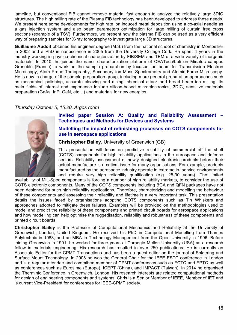
Guillaume Audoit obtained his engineer degree (M.S.) from the national school of chemistry in Montpellier in 2002 and a PhD in nanoscience in 2005 from the University College Cork. He spent 4 years in the industry working in physico-chemical characterization by FIB/SEM and TEM of a wide variety of inorganic materials. In 2010, he joined the nano- characterization platform of CEATech/Leti on Minatec campus Grenoble (France) to work on the sample preparation by focused ion beam for Transmission Electron Microscopy, Atom Probe Tomography, Secondary Ion Mass Spectrometry and Atomic Force Microscopy. He is now in charge of the sample preparation group, including more general preparation approaches such as mechanical polishing, accurate cleaving and dicing, chemical attack and broad beam ion milling. Its main fields of interest and experience include silicon-based microelectronics, 3DIC, sensitive materials preparation (GaAs, InP, GaN, etc…) and materials for new energies.
Thursday October 5, 15:20, Argos room Invited paper Session A: Quality and Reliability Assessment – Techniques and Methods for Devices and Systems Modelling the impact of refinishing processes on COTS components for use in aerospace applications Christopher Bailey, University of Greenwich (GB) This presentation will focus on predictive reliability of commercial off the shelf (COTS) components for high reliability applications in the aerospace and defence sectors. Reliability assessment of newly designed electronic products before their actual manufacture is a critical issue for many organisations. For example, products manufactured by the aerospace industry operate in extreme in- service environments and require very high reliability qualification (e.g. 25-30 years). The limited
availability of MiL-Spec components is forcing a number of high reliability markets, to consider the use of COTS electronic components. Many of the COTS components including BGA and QFN packages have not been designed for such high reliability applications. Therefore, characterizing and modelling the behaviour of these components and assessing their reliability and lifetime is a very important task. This presentation details the issues faced by organisations adopting COTS components such as Tin Whiskers and approaches adopted to mitigate these failures. Examples will be provided on the methodologies used to model and predict the reliability of these components and printed circuit boards for aerospace applications and how modelling can help optimise the ruggedisation, reliability and robustness of these components and printed circuit boards.
Christopher Bailey is the Professor of Computational Mechanics and Reliability at the University of Greenwich, London, United Kingdom. He received his PhD in Computational Modelling from Thames Polytechnic in 1988, and an MBA in Technology Management from the Open University in 1996. Before joining Greenwich in 1991, he worked for three years at Carnegie Mellon University (USA) as a research fellow in materials engineering. His research has resulted in over 250 publications. He is currently an Associate Editor for the CPMT Transactions and has been a guest editor on the journal of Soldering and Surface Mount Technology. In 2008 he was the General Chair for the IEEE ESTC conference in London and is a regular attendee and committee member of CPMT conferences such as ECTC and EPTC as well as conferences such as Eurosime (Europe), ICEPT (China), and IMPACT (Taiwan). In 2014 he organised the Therminic Conference in Greenwich, London. His research interests are related computational methods for design of engineering components and systems. Chris is a Senior Member of IEEE, Member of IET and is current Vice-President for conferences for IEEE-CPMT society.

19
ESREF 2015 Tutorials Within the frame of ESREF 2015, we offer a series of attractive tutorials on important issues of electronics. Since avionic and aeronautic applications are in focus of this year’s conference, related tutorials deal with reliability and power electronics as well as PCB- and system-related analysis and anamnesis approaches towards root cause finding. Take the opportunity looking beyond the scope of device-related failure analysis by learning from experienced tutorialists from industry and research. In order to allow tutorial access independent from competing parallel sessions, the tutorials are embedded as plenary sessions within the regular program. We look forward to welcoming you there.
Tuesday October 6 - 8:20, Guillaumet room
Tutorial Session E1: Packages & Assembly
T1. Minimizing Defects by Design for Soldering Thomas AHRENS, TrainAlytics GmbH, Germany Soldering is by far the most used joining technology for electronic assemblies on printed circuit boards. With small pitch, lead-free soldering and hidden solder joints there are strong challenges and process issues to keep solder defect rates low. Observing certain design rules helps a lot. This tutorial presents key points in geometry of solder lands, material and process tolerances, paste volume vs. solder fillet volume, and needs for process control. You will learn how to classify and count solder defects and be able to sort them according to possible origin. In many cases there are checklists available from various IPC standards, which give a base or a starting point for an appropriate technological approach. Target groups for this tutorial are designers, process and quality specialists and managers. It provides design for manufacturing procedures to enhance the productivity of electronic assemblies, thus reducing the probability of solder defects.
Dr. Thomas Ahrens is active as consultant in the field of quality and reliability, production and repair of electronic assemblies. On a background of materials sciences, he has over 25 years of reputation in trouble shooting and qualification of materials, processes and personnel. His work methods include customized on-site investigation, mediation of seminars, workshops and practical training for industry clients. Dr. Ahrens collects his experiences from a rich fund of public research and development projects, and quality and damage analysis cases. Dr. Ahrens is Master Trainer for IPC-A-610 and J-STD-001 and chairs the DVS thematic group FG 4.11 Education in Solder Process for Electronic Assemblies. Dr. Ahrens is Managing Partner of Trainalytics GmbH, DE-Lippstadt, a company serving electronics industry in employees training,
product quality and physical defect analysis.
Tuesday October 6 - 9:20, Argos room Tutorial Session E2: MEMS, MOEMS, NEMS & Nano-objects
T2. MEMS Failure modes, FA and reliability challenges Jérémie DHENNIN, Elemca, France Challenges in the successful industrialization of MEMS devices are probably now related to their reliability. When lifetime is a first order criterion, reliability should be addressed since the early stages of development. The purpose of the tutorial will be to introduce the methodologies to evaluate the reliability of MEMS devices, as well as the conventional or custom techniques that can be used for that purpose. Indeed, the standard approaches for reliability assessment or qualification of microelectronics devices are insufficient to account for the MEMS peculiarities (multi-physical effects). A case study on RF-MEMS devices will be presented during the tutorial.

20
Jeremie Dhennin received his master degree in Micro and Nano Physics from the university of Paul Sabatier in Toulouse, France in 2005. He joined NOVAMEMS as a research engineer working on multi-physical characterization and modeling of MEMS switches failure mechanisms. His research activities focused on RF MEMS switches reliability, failure analysis and modeling, especially dealing with micro-contact issues. Since 2012, his technical scope has evolved to more generic reliability issues, dealing with other types of MEMS or electronic components. His managerial experience and broad technical scope has allowed him to take the CEO position at FIALAB – now ELEMCA – at the beginning of 2013.
Tuesday October 6 - 14:20, Guillaumet room Tutorial Session E1: Packages & Assembly
T3. Avoiding Flex Cracks in Ceramic Capacitors (CerCaps): Analytical Tool for a Reliable Failure Analysis and Guidance for Positioning CerCaps on PCBs Gert VOGEL, SIEMENS AG (Germany) In every electronic assembly line where ceramic capacitors are used and printed circuit boards are de-paneled the quality risk “flex cracks” is known. Unfortunately flex cracks in ceramic capacitors (cercaps) always extend under the metal terminations of the capacitors and electrical tests do only reveal about one percent of the affected parts. With a new method – etch away the terminations and look at the otherwise hidden cracks – it is possible to identify all sources of mechanical bending and warping. In the course of failure analysis is it helpful to know that most times not only the failed ceramic capacitor shows a crack pattern but also all the surrounding cercaps as well. Well-founded knowledge about different crack patterns
and failure modes also allows recognizing unsafe bending and warping lines on the PCB. This gives us a guidance to place the ceramic capacitors in optimal orientation not only to de-paneling lines but also in the vicinity of mounting and screw openings. Finally the different kinds of cercaps with internal layouts that prevent boards from failing even if flex cracks should show up are reviewed.
Dr. Gert Vogel has been with Siemens more than 30 years. Seven years he has been a semiconductor technologist in the Siemens DRAM production in Munich and Regensburg. Then he moved to Siemens Amberg where amongst other topics he is a specialist for failure analysis of electronic components.
Tuesday October 6 - 16:40, Cassiopee room Tutorial session G: Space, Aeronautic and Embedded Systems
T4. Radiation effects on components at space level Robert ECOFFET, CNES, France The space radiation environment is a major constraint in satellite design and a source of many in-flight anomalies. In this communication, we will start with a brief overview of the space radiation environment. Then we will review the state of the art of major effects of radiation on electronic components, as taken into account in space projects today. This part of the talk will be illustrated by examples of radiation-induced spacecraft anomalies. In a third part, we will try to appreciate the possible new challenges brought by technology downscaling and the introduction of new materials and concepts. Finally, we will describe the “radiation hardness assurance” in space projects and highlight the steps where improvements and margin optimization could be made in this engineering process.
Robert Ecoffet was born in Marseille, France, on July 22, 1963. He graduated in 1987 with an engineer degree from the Ecole Supérieure d’Electricité, Gif sur Yvette, France, with a specialization in electronic properties of materials. After serving in the French Marine for his National duties, he joined as an engineer the French Space

21
Agency CNES (Centre National d’Etudes Spatiales). Since 25 years, he has been working for CNES in the field of space environment and radiation effects. He participated extensively in radiation testing and project support in this field, leaded many radiation effects and space environment modeling research activities, was responsible for the development of space environment and technological experiments, and was part of many spacecraft anomalies investigation teams. He co-authored more than 100 papers mainly published in the IEEE Transactions on Nuclear Sciences. He is a member of the RADECS Association (Radiation Effects on Electronic Components and Systems) steering board, and had the honor to serve as General Chairman of the 2014 IEEE Nuclear and Space Radiation Effects Conference. His position in CNES is senior expert in space environment and radiation effects, and responsible for CNES “space environment” R&D axis.
Tuesday October 6 - 17:20, Cassiopee room Tutorial session G: Space, Aeronautic and Embedded Systems
T5: Radiation and COTS at ground level Jean-Luc AUTRAN, Daniela MUNTEANU, Aix-Marseille University, CNRS, IM2NP, France This tutorial will survey single event effects (SEE) induced by terrestrial cosmic rays on current commercial CMOS technologies. After describing the natural radiation environment at ground and atmospheric levels, the tutorial will describe the physics of SEEs, from the main mechanisms of interaction between atmospheric radiation (neutrons, protons, muons) and circuit materials to the electrical response of
transistors, cells and complete circuits. SEE characterization using accelerated and real-time tests will be examined, as well as modeling and numerical simulation issues. Special emphasis will finally concern the radiation response of advanced technologies, including deca!nanometer bulk, FD!SOI and FinFET families.
Jean-Luc Autran is distinguished professor of physics and electrical engineering at Aix-Marseille University and honorary member of the University Institute of France (IUF). He is also deputy director of the Institute for Materials, Microelectronics, and Nanosciences of Provence (IM2NP, UMR CNRS 7334) and the principal investigator of the Altitude Single-event effects Test European Platform (ASTEP). His current research interests focus on the physics of soft errors, from the characterization of natural radiation to Monte Carlo radiation
transport simulation. He is the author or coauthor of more than 300 papers published in international journals and conferences, and has supervised 28 Ph.D theses.
Daniela Munteanu is director of research at the National Center for Scientific Research (CNRS). She is a
fellow researcher at the Institute for Materials, Microelectronics, and Nanoscience of Provence (IM2NP, UMR CNRS 7334) and has 15 years of experience in characterization, modeling, and simulation of semiconductor devices. Her current research interests include emerging complementary-metal-oxide-semiconductor (CMOS) devices, compact modeling, numerical simulation in the domains of nanoelectronics, and radiation effects on components and circuits. She is also the author or coauthor of more than 200 papers published in international journals and conferences, and has supervised 12 Ph.D theses.
Wednesday October 7 - 14:20, Spot room
Tutorial session C: Failure Analysis

22
T6. FA (=Failure Analysis and Anamnesis) and reliability at system level Peter JACOB, EMPA Duebendorf, Switzerland Most failure analysts are used to do failure analysis on device level but they hardly know about failure analysis and anamnesis on system level. Many device failure analysis wrap up with EOS, which in most cases also means “end of story”. However, looking at root cause findings, a majority of device failures result from circuitry transients, environmental conditions or from passive component failures, which produce shorts or lose their protection function. The tutorial shows up systematic approaches on failure anamnesis, which ideally guides towards the failure root cause by a careful application evaluation. Numerous examples illustrate the methodology. In this context, classical device analysis becomes just a supporting function of the anamnesis, which includes statistical and physical failure occurrence, reliability aspects, reverse FMEA and fact sheet analysis. The goal of the tutorial is to open the device-minded view of failure analysts towards the operational environment, mission profiles and system-related physics-of-failure.
After studying Technical Physics in Munich, Peter Jacob started his professional work in 1981 as a failure analysis expert in IBM semiconductor plant Boeblingen until 1992. After a short period at Hitachi Scientific Instruments, where he was responsible for electron microscopy configurations and customer trainings, he joined ETH Zurich/ Empa as a senior expert for failure analysis on micro- and power-electronics from device to system level. In parallel to this work, in 1995 he joined to Swatch Group – EM Microelectronic Marin as a principal F/A engineer. Jacob has authored more than 60 contributed and invited papers including an ESREF Best Paper. He volunteers in the German ESD Forum, EDFAS and EuFANet. In 2007 he was appointed to a Honorary Professor of Technical University Munich and in 2010 he received the International Barkhausen Award of Technical University Dresden.
Wednesday October 7 - 16:40, Guillaumet room Tutorial session F: Power Devices
T7. Mission profile and reliability on power electronics Prof. Ke Ma and Prof. Huai WANG, Aalborg University / Peter de PLACE RIMMEN, Danfoss Power Electronics In many mission-critical applications of energy conversions such as renewables, electricity transmission, electric vehicles, and aircrafts, etc, the power electronics should be extremely reliable and robust to avoid high cost of failures. In order to meet this challenging requirement, there is an ongoing paradigm shift in this field from the statistics-based assessment to the physic-of-failures based analysis. In this shift the stress and strength models of the power electronics components need to be accurately built, and both of the factors are closely related to the operating conditions or mission profiles of the whole systems. These mission profiles will involve multi-disciplinary knowledge and new approaches for the design of reliability performances. In this tutorial an overview of the involved data for specifying reliability for a new product development will be first given, and the importance of mission profiles for the reliability R&D is emphasized from industry perspective. Afterwards a flow and structure, which can translate the mission profiles of applications to the reliability metrics of power electronics, is proposed with practical examples. And some emerging challenges and requirements for the reliability testing/validation are also addressed. Finally the potential methodologies and technology trends involved with mission profiles based reliability analysis are also discussed.

23
Ke Ma is currently an Assistant Professor at Aalborg University with the Center of Reliable Power Electronics (CORPE), where he is the leader of working package 4 involving reliability modeling and design tools development. His research interests are power electronics technology including reliability in the applications of power generation and consumption systems. In the last 4 years he has contributed more than 50 journal and conference papers including 4 book chapters in the field of power electronics and reliability. He is one of the lecturers for an Industrial/PhD course on “Reliability in Power Electronic Systems” at Aalborg University, and was invited as speaker at two of the European Center for Power Electronics (ECPE) workshops. Dr. Ma received the B.Eng. and M.Sc. degrees from Zhejiang
University, China and PhD degree from Aalborg University, Denmark. He was the receiver of the Excellent Young Wind Doctor Award 2014 by European Academy of Wind Energy, as well as a few IEEE prized paper awards. He is now serving as Associate Editor of IEEE Transactions on Industry Applications.
Huai Wang is currently an Assistant Professor with the Center of Reliable Power Electronics (CORPE) in the Department of Energy Technology, Aalborg University, Denmark. His current research interests include the reliability of power electronic systems and reliability of capacitors in power converters. He was one of the lecturers for a PhD course on Reliability in Power Electronic Systems at Aalborg University and was an invited speaker at the ECPE workshop on lifetime modeling and simulation. He has contributed a number of journal papers, including several concept papers on the design for reliability of power electronic systems. Dr. Wang received his PhD degree from the City University of Hong Kong, Hong Kong, in 2012. He is a Visiting Scientist with the ETH Zurich, Zurich, Switzerland, from August to September 2014 and with the Massachusetts Institute of Technology (MIT), Cambridge, MA, USA, from September to November 2013. He was with the
ABB Corporate Research Center, Baden, Switzerland, in 2009. He serves as an Associate Editor of IEEE Transactions on Power Electronics, and a Guest Associate Editor of two special issues on topics relevant
to reliability in power electronics.
Peter de Place Rimmen is today Reliability Advisor at Danfoss Power Electronics A/S in Denmark. His experience is coming from total 42 years with R&D. Totally 7 years as designer, 9 years with management and during the last 27 years Peter has worked with practical approach implementing Reliability in followed companies: Vestas Wind System R&D form 2004 to 2009, Grundfos Management from 1997 to 2004 and Bang & Olufsen R&D from 1988 to 1997. Before that he had careers at B&O as constructor, Test engineer, Plant manager and Project manager. Peter had for some time participated in IEC dependability group. Peter has together with Nokia trained Nokia R&D and Vestas R&D people around the world in “Design for Quality and Reliability”. Today Peter is participating in “CORPE” Centre of Reliable Power Electronics at Aalborg
University, Teaching 2th Master Class at Aalborg University Dep. Energy Technology in modern reliability, participating in ZVEI “Facts Sheets Group”, board member FAST (Danish Society for Applied Statistics) and initiated in 2001 and member of the Danish Six Sigma ERFA-group, subgroup of FAST. Member of the Danish Reliability group (SPM-6) since 1988.
! !

24
!
!
Thursday October 8 - 11:00, Argos room
Tutorial session A: Quality and Reliability Assessment – Techniques and Methods for Devices and Systems
T8. Integrated Vehicle Health Management (IVHM) for Aircraft Electronics/Power Electronics Suresh PERINPANAYAGAM, Cranfield University, UK Integrated Vehicle Health Management (IVHM) is the transformation of system data on a complex vehicle or system (such as a luxury car or a commercial airplane) into information to support operational decisions and optimize maintenance. IVHM is a capability, comprising a number of technologies that can be used across a number of sectors for business benefit. IVHM is becoming increasingly important as OEMs (Original Equipment Manufacturers) move from the traditional sale of a product, in which future income is dependent on spare part revenue, to selling a service in which steady monthly income can be derived in return for the effective maintenance of the asset. IVHM enables this transformation. The IVHM Centre delivers generic IVHM solutions including capability to sense, detect, diagnose, and predict imminent degradations or failures in vehicles, thereby allowing the evaluation of the reliability of the systems under real application environments. This tutorial will focus on investigating the capability of health monitoring techniques to detect degradation of electronic and power electronics in an integrated avionic system.
Dr Suresh Perinpanayagam leads the ePHM Group, part of the Boeing Integrated Vehicle Health Management Research Centre set up by The Boeing Company. Suresh has rapidly established a research group, managing 14 researchers (2 research fellows, 6 full-time PhDs, 2 MSc by research and 4 MSc by taught course students) and has obtained grants amounting to £1.4M in total from industrial, EPSRC, TSB and EU-FP7 projects. Suresh obtained his Master in Engineering and PhD in Engineering at Imperial College, London. Suresh has spent considerable time in industry working on various industrial R&D projects. Suresh’s vision is to create every electronic system with its own brain to be self-aware of its own health state and to work effectively with other systems to
complete a function even if it is not in an optimal state. To realise this, the group develops tools to detect the inception of failures in electronic components and track them to system failures. They also need to correlate the fundamental physics-of-failure work currently done at material science level (for example, solder joint and wire bond failure) to the electronic system data acquired for system health management from data-centric aircrafts, such as Boeing 787. These intelligent electronic systems will inform and reconfigure its health state at different stages of its life. These new systems will redefine the current Built-In Test (BIT) technology in electronic systems with more user-friendly, reduced no-fault-found rate, reduced repair, reduced cost, predictable failures and greater availability for industry. The ePHM group has links with many of the UK’s high value added electronic system manufacturers, including AEC, Thales, Selex, BAE Systems, Meggitt, GE, Honeywell, Cassidian, General Dynamics, UTC, Raytheon and Visteon Corporation. The group uses this forum to connect fundamental research issues in material, design, manufacturing process, testability, system issues and through-life management of these electronic systems.

25
ESREF 2015 Workshops According to its tradition, ESREF continues to provide an interactive forum to the participants to define the state-of-the-art of leading subjects in the reliability field. Workshops, mini-workshops, and round tables are offered to the participants for no fee.
Chip level Advanced Failure Analysis case studies Tuesday October 6 - 11:00 to 16:00, Spot room
Sector Technologies Workshop organized by Jean-Philippe ROUX, Sector Technologies (France)
On rather mature technologies, FA engineers have been able to come with new innovative approach and applications. This workshop will present a subset of these new advanced and surprising applications. All presentations will be done on final user real test cases :
• Thermal phenomena propagation Elite case studies • Lockin thermography Elite case study • Picoseconds pulsed laser applied to radiation testing • Low noise nanoprobing measurement on 28nm technology • Spectroscopy application with InGaAs on Meridian IV
Student Research Speed Dating Tuesday October 6 - 11:00 to 12:20, Argos room
Organized by Thomas ZIRILLI, Freescale (France)
Professionals will meet with selected PhD and Masters students that will present their advanced work on reliability and failure analysis on electronics. Let us meet the talents of tomorrow.
Anthony BOSCARO, Le2i, University of Burgundy, Dijon, France, CNES, Toulouse, France Improvement of Failure Analysis equipments by incorporating signal/image processing tools Chung Tah CHUA, School of Materials Science and Engineering, Nanyang Technological University, Singapore, CNES, Toulouse, France Reliability Meets Radiation Hardness Giulia MARCELLO, Department of Electrical and Electronic Engineering, University of Cagliari, Italy, Evidence for proton diffusion in H+ irradiated DFB and VCSEL commercial laser diodes. He HUANG, LAAS-CNRS, France EMC (electromagnetic compatibility) reliability Kokou ADOKANOU, CEMEF MINES ParisTech, UMR CNRS 7635, PSL Research University, Sophia-Antipolis, France, CNES, Toulouse, France, Thales Alenia Space, Toulouse Investigation on the effect of external stress on the DC characteristics of GaAs microwave Maxime PENZES, ST Microelectronics, Crolles, France, Development and optimization of new qualitative optical techniques for fast and sure default localization on FD SOI and Bulk advanced technologies Norimichi CHINONE, Research Institute of Electrical Communication, Tohoku University, Japan, Development of method for local C-V curve measurement and its applications Paula DIAZ REIGOSA, Center of Reliable Power Electronics (CORPE), Aalborg University, Danemark, Failure Mechanisms of Semiconductor Power Devices Operated under Short Circuit Conditions Roberta PILIA, IntraSpec Technologies, France Pulsed laser stimulation of Si components in order to assess their sensitivity to the impact of heavy ions. Roberta RUFFILLI, CEMES, Toulouse, France, Freescale, Toulouse, France, In-depth investigation of metallization aging in power MOSFETs Thomas LOMBARDI Freescale, Toulouse, France Advanced Deprocessing technique for Gate oxide investigation

26
Modeling the reliability at system level : tools and methodology
Tuesday October 6 - 13:40 to 16:00, Cassiopee room
Oganized by Nicolas NOLHIER, LAAS-CNRS (France) and Gilles PERES, Airbus Group Innovations (France)
• “Methodology to characterize and model ageing effect on components’ EMC behavior (Emission and Immunity)”, André DURIER, IRT Saint Exupéry (France)
• “Methodology to model components immunity towards ESD and electrical transients”, Patrice BESSE, Freescale (France)
• “IEC ICEM (Integrated Circuit Emission Model) & ICIM (Integrated Circuit Immunity Model)” or “Evolution of EMC requirements in avionics”, Christian MAROT, Airbus Group Innovations (France)
• “Improved ESD test method for testing spacecraft equipement”- Patrice PELISSOU, AIRBUS Defense & Space (France).
Advanced tools and techniques flash presentations Mini-Workshops organized by Fulvio Infante, Intraspec Technologies (France).
Methods and tools for Failure Analysis and Reliability Tuesday October 6, 8:40 – 9:20, Argos room
“Tools for Multichannel, phase sensitives Failure Analysis modes”, Romain Stomp, Zurich Instruments (Switzerland) “Failure Analysis Going Towards Anamnesis - a Holistic Approach for Successful Root Cause Detection”, Jürgen Gruber, RoodMicrotec (Germany) Today’s failure analysis show, that only approx. 10% of the root causes are related directly to the failed component. In most cases the failing of the component is only a consequence of a production, assembly or application related problem. Knowing about this background, the way of failure analysis must be changed to anamnesis, which has to cover all relevant issues like failure history, application conditions, packaging, board assembly, subsystem and system information. The presentation will give an overview about the distribution of the significant failure causes, an overview about fields which have to be included for the anamnesis and will show some examples of successful anamneses. “A Technology Research Institute for Aeronautics, Space and Embedded”, Régine Sutra-Orus, IRT Saint Exupéry (France) IRT Saint-Exupery is a French multidisciplinary institute based on a private-public partnership and dedicated to build and manage world class technology research projects in key technologies : More Electrical Aircraft, Embedded Sytems, multifunctional and high performance Materials . IRT Saint Exupery provides an integrated collaborative environment fitting into the research landscape and technological platforms accelerating innovation and transfer to industry. A focus will be given to More Electrical Aircraft technologies including the characterization and modeling of the components’ reliability and also of the physics phenomena having impact on the reliability of the whole electrical system.

27
Fault isolation - defect localization Tuesday October 6, 9:40 – 10:20, Spot room
“Extended Sensitivity NIR Camera for Photon Emission Microscopy of ICs”, Andrea Bahgat-Shehata, Franco Stellari, Alan Weger, Peilin Song, IBM (USA), Herve Deslandes, Ted Lundquist DCG Systems (USA) and Antoine Reverdy, Sector Technologies (France). A photon emission microscopy (PEM) camera has been characterized for acquiring photons emitted from ICs during normal switching events. This camera was designed for sensitivity at longer wavelengths so as to maximize signal intensities from low voltage ICs [1-3]. In this paper, we characterize the performance of the camera using 32 nm and 22 nm SOI chips. This camera can collect emission images from ICs operating at voltages down to 0.5 V, far exceeding the performance of state-of-the-art InGaAs cameras. “New Tools for Defect Analysis : Lock In IR Tomography and Cost effective test solutions for digital products”, Gerald Guibaud, Thales (France) Defect analysis techniques evolves following users’ needs towards cost and time to market solutions. Thales Communications & Security has now the capability to propose upstream solutions like Lock In IR tomography to investigate quicker on ( PCB’s, chips, power components, solar cells, …) defects and also more cost effective and portable test solutions to reveal electrical defect and/or characterize complex digital products as Memories, Image sensors, System on chips(SoC), Digital ICs (FPGAs, audio & video processors…) “Case Studies of EOP/EOFM (Electro Optical Probing and Frequency Mapping)”, Yoshitaka Iwaki, Hamamatsu (Japan) We have developed EOFM (Electro Optical Frequency Mapping) and EOP (Electro Optical Probing) for failure analysis. The EOFM enables you to visualize transistor operation as 2D image. And the EOP enables you to probe wave form at transistors. At the presentation, I will introduce the basis & features of the techniques and some case studies from customers. “Use of advanced localization techniques for fault isolation on packages and dies: Magnetic Current Imaging, Lock-in Thermography, Time Domain Reflectometry and X-Ray Computed Tomography”, Fulvio Infante and Nicolas Courjault, Intraspec Technologies (France) Very often, the use of one single technique for defect localization is not enough. More and more often, we need to couple the use of several techniques in order to precisely localize defects in advanced technologies. We dispose in our lab of a wide set of those: we will show how a set of them can be used to solve complicated localization problems. Sample Prep Tuesday October 6, 16:40 – 17:20, Spot room "Comparison of decapsulation techniques for Copper and Silver wires’’, Patrick Poirier and Michael Obein, Digit-Concept (France) The ICs have known lot of evolution in the past years due to the introduction of new materials like Cu or Ag wires and the emergence of complex modules and Systems in Package. To meet the decapsulation challenges of these ICs, many studies and many improvements have been done recently. We will give an overview of techniques available and the solutions we propose to solve the issues that are facing the Failure Analysis Laboratories. “Repeatable method for automated decapsulation of silver alloy wire packages”, Matthew Lefevre, JP Kummer (France), Emmanuel Noraz and Damien Veychard, STMicroelectronics (France)

28
Over the past several years there has been a large industry wide effort to change over from gold bonding wires to copper in order to minimize production costs. In certain cases this is not possible due to the relatively high hardness values of Cu, which leads to reliability issues in the manufacturing process. Silver (Ag) wire has been proposed and successfully implemented in many instances where Cu wire was not practicable. Unfortunately, currently integrated decapsulation methods severely damaged or destroyed the silver wires and bonds, making it impossible to perform production controls and failure analysis. Here we present a reliable and repeatable automated method to expose these die and wire bonds by adding a dilute iodine solution to the nitric acid in an acid decapsulator. “New Methodologies for High Accuracy Cleaving (HAC) and Scribing to Speed Time to Analysis Ready Samples”, Efrat Moyal, LatticeGear (USA) Increasing complexity combined with shrinking geometries in electronic devices have placed new demands on the sample preparation process. Much effort must be made to assure that the sample preparation process delivers data and does not alter the sample structure or material properties. This presentation will introduce a new method for high accuracy cleaving and scribing methods for cross sectioning targets to 10 µm accuracy without altering the properties of the sample. Unique micro line indentation method will be demonstrated for cleaving semiconductor wafer and wafer pieces, and scribing/cleaving for FlipChip or backside devices. “Versatile Sample Preparation Tool That Enables Access to Devices for Complex Device Electrical Failure Analysis”, Chris Richardson, Allied High Tech Products (USA) Ceramics to plastic encapsulated devices, multi-chip modules to 32 layer stacked die, from 0.5 mm x 0.5 mm area devices to 40 mm x 40 mm devices, having a versatile sample preparation tools is critical to enabling electrical failure analysis. Discover through a series of case studies how one tool can provide the right chip access solution for most any sample type. “The use of interactive capacitive and resistive electrical end-pointing techniques for pre-cavitation of packaged IC’s”, Matthew Lefevre, JP Kummer (France). Using a thinning/polishing tip whilst measuring capacitive build-up allows for interactive decapsulation of overmolded IC packages allows for a closer (safe) end-point than using LASER decap methods. Mechanical decapsulation also offers the added benefit of automated tilt alignment, offering a uniform mold compound layer as a starting point for final decapsulation with plasma-based techniques. Real examples will be shown to illustrate the technique. Non Destructive Testing and Physical Characterization Tuesday October 6, 17:20 – 17:55, Spot room
“When warpage measurements help FA and FEM at the same time!“, Diane Ecoiffier, Insidix (France) Presentation of case studies regarding warpage and thermal expansion measurements. Discover how they are used to implement models for lifetime simulation and reliability work. With a briefly introduction to TDM technology, we will show two examples of work with measurements and simulation – exchanges between both to improve model, to choose a supplier or a base material (eg. glue or mold). “Reliability evaluation of electronic solder joints (lead-free), thanks to microstructural analyses (SEM-EBSD) on new vs aged BGAs”, Clovis Lataste and Romain Petre-Bordenave, Elemca (France) Lead-free solder joints are widely used in automotive or consumer applications, and it will be probably the case also in the aerospace industry in the next years. Yet specific failure mechanism

29
occurs, driven by the metallurgy of the alloy. If accelerated aging through thermal cycling is generally used to monitor the ageing of the soldering, other investigation techniques like EBSD imaging provide interesting inputs to evaluate their reliability. A case study will be proposed to present the results of EBSD investigation on lead-free solder joints. “Laminography, a high resolution technique for imaging object slice”, P. Serre and N. Paillet, Predictive Image (France) X-ray tomography is well known as a non-destructive method for technical components analysis. However, this technique has its own limitations when large objects have to be analyzed with high resolution. Here, we present an alternative to tomography: a system of translatoric or rotational laminography, which allows imaging 2D object slices. By using these systems of laminography, it is possible to inspect at large 2D multi layer or to dissociate two components face to face on a printed circuit for example. Thus, this technique expands the capacity of 3D reconstruction with X-Ray methods. “Scanning acoustic microscope: new technologies in failure analysis”, Kasim Altin, PVA TePla Analytical Systems GmbH (Germany) For reliability determination a nondestructive method such as scanning acoustic microscopy is technology of choice. However, this method has its own limitations, e.g. when depth and resolution have to be combined to cover the target. This presentation will show how to overcome these challenges and limitations using new methods (e.g. intelligent auto focus axis, advanced signal processing and higher sampling rate….). Nanoscale electrical measurement Tuesday October 6, 17:55 – 18:20, Spot room
“Constant Voltage Electromigration (CVEM)”, Eric Wilcox, Cascade Microtech (USA) CVEM as an alternative method to constant current EM for BEOL reliability test, especially for advanced interconnects with extremely-scaled, non-conductive barriers found in CMOS technologies below the N-10 node. CVEM advantages include truer lifetime prediction, by preventing unrealistically high voltages over voids when current shunting through the barrier is not available, and reduced distributional shape for higher statistical certainty. The CVEM testing was performed in cooperation between IMEC and Cascade Microtech. “Effortless nanoprobing by correlative microscopy using the combination of SEM and SPM”, Andrew Jonathan Smith, Kleindiek Nanotechnik (Germany) “Oxide breakdown and dielectric weak point localization using robotic nanoprobers coupled with EBAC”, Vincent Faivre, Imina Technologies (Switzerland)
OEMs for components providers Wednesday October 7 - 8:00 to 10:20, Cassiopee room
Round table organized by Olivier Crépel, AIRBUS Group Innovations (France) and Thomas Zirilli, Freescale Semiconductor
Panelists: S. Bailly, Airbus Helicopters RAMS (France) and A. Quemener, Airbus Defence & Space component selection (France)
Taking advantage of the organization of ESREF in Toulouse, the cradle of Airbus, aeronautics end users of electronics propose to hold a round table on the requirements they have as far as microelectronics and components are concerned. Animated by Airbus, and with the participation of specialists from Airbus

30
Helicopters, Airbus Defence & Space and others, the round table will be an opportunity to exchange on the qualification standards imposed on avionics. Specialists in RAMS and component selection from aeronautics will discuss how the reliability and qualification stringent conditions shall be understood and what are the consequences at component or equipment suppliers’ level. It may be an opportunity for suppliers to better understand how they may serve the avionics market.
DSM Technology impact on safety assessment Wednesday October 7 - 11:00 to 12:20, Cassiopee room
Organized by Didier Régis, Thales Group (France)
For more than 40 years, Gordon Moore’s experimental law has been predicting the evolution of the number of transistors in integrated circuits, thereby guiding electronics developments. Until now, this evolution did not have any measurable impact on components’ quality; but the trend is beginning to reverse. In this session, we are going to address the impact of scaling on the reliability of integrated circuits with a focusing on three basics of safety analyses for aeronautical systems: failure rates, lifetimes and atmospheric radiations’ susceptibility.
Failure Analysis of Critical Systems Wednesday October 7 - 16:40 to 18:20, Spot room
EUFANET Workshop organized by Jérome Touzel, Infineon (Germany) and Olivier Crépel, AIRBUS Group Innovations (France).
Systems failure occurs when a system does not meet its requirements. A laser failing to designate its target, an aerial refueling system failing to transfer fuel at the proper flow rate, a blood chemistry analyzer failing to provide accurate test results, a munition that detonates prematurely, and other similar conditions are all systems failures. Systems failure analysis is an investigation to determine the underlying reasons for the nonconformance to system requirements. Critical systems are systems which reliability is mandatory : Transmission control unit or brakes electronics in a car, computers in a satellite, Engine controls in a plane, etc.. System level FA is quite complex as it has to apprehend system environment to understand the root cause of the failure, and usually harsh environment for plane, car, train, rockets, etc..
European FIB Users Group workshop Thursday October 8 - 11:00 to 17:40, Spot room
Organized by Hugo Bender, IMEC (Belgium)
In addition to the conference FIB session on Thursday morning a more practically oriented workshop is organized on Thursday as well. Contributions for the FIB workshop are welcome that relate to practical topics, new developments and application examples of semiconductor applications of FIB :
• New instruments : HIM, Plasma-FIB, Laser preparation tools • Efficient preparation workflows : automated TEM preparation, Plasma-FIB, Laser, atom probe
sample preparation, ... • Circuit edit : application procedures, new gas chemistries, ... • Process monitoring for wafer manufacturing, in-line FIB and wafer return • Failure analysis case studies : Si devices, wide bandgap, solar cells
Oral presentations: ! Matthias Kemmler et al, Failure Analysis in FIB/SEM - Locating Failures and performing

31
Nanoprobing in situ ! David Donnet et al, Gas Assisted Plasma FIB Delayering of Advanced Semiconductor Devices ! Matthieu Viteau et al, Laser cooled atoms as a focused ion beam source ! Peter Meis et al, FIB daily business at Infineon
Poster presentations :
! Lorenzo Motta et al, FIB device surgery for noise reduction in InGaAs/InP SPAD arrays ! Hugo Bender et al, Mechanism of surface redeposition and electrical damage during FIB milling ! Patricia Van Marcke et al, Plan view specimen preparation with FIB
Reliability of avionics power electronics Friday October 9 – 8:30 to 12:30, Spot room
ECPE Annual Workshop on Power Devices organized by Eckhard WOLFGANG, ECPE (Germany)
There is quite a lot of progress in automotive and industrial applications regarding qualification of power modules based on the Robustness Validation Process, which includes Mission Profiles, End-of Life Testing and Physics of Failure. Workshop agenda is:
Introduction, Eckhard Wolfgang, ECPE
! Robustness Validation Process, Eckhard Wolfgang, ECPE ! Mission Profile for Solar and Wind, Huai Wang, Univ Aalborg, CORPE ! Translation from system to PE mission profile, Jochen Koszescha, ECPE ! How different skills interact ensuring reliability, Peter de Place Rimmen, Danfoss ! Discussion Part 1
Coffee Break
! Partial discharge in aeronautic environment, Thibaut Billard, More Electrical Aircraft- IRT Saint Exupery
! Heavy ion impact on GaN transistors, Moustafa Zourarka, More Electrical Aircraft- IRT Saint Exupery
! Multistress reliability model for GaN, Alain Bensoussan, More Electrical Aircraft- IRT Saint Exupery
! Fault tolerant power modules, Kai Kriegel, Siemens ! Power Cycling of SiC-MOSFET power modules, Zoubir Khatir, IFSTTIR ! Thermal Management of Satellite Elctr. William Serrano, Airbus Defense&Space ! Discussion Part 2
Conclusions The structure of the annual WS is: 1) Short statements for each topic (3-4 slides) 2) The audience will be asked to name their most interesting topics 3) In depth explanation and discussion of those topics 4) Summary
Design and test for robustness and reliability Friday October 9 – 8:30 to 12:30, Argos room
Organized by Philippe Perdu, CNES (France)
This workshop aims to cover these wide topics from a component user point of view and should address all

32
the related topics (Safety, Security, Environment: EOS, ESD, EMI, radiation, temperature …). It concerns design and test for reliability and robustness purposes on high reliability / critical embedded systems (automotive, aerospace, transportation, energy, health …).
This workshop will be devided in 3 Parts. Each part will start with a specific lecture one one topic followed by open discussion / Round table
Design for reliability (PCB, subsystem level) Just enough technology consolidated by the Design IPC standards
Sylvain Leroux, Jetware
Designing For Reliability in design-chain means considering all the factors necessary to establish the probability that a board will function properly for a defined period of time under the influence of operational condition. Heat and thermal cycling are the enemies of Board performance and long term reliability … for an IPC Certified Interconnect Designers (CID/CID+), managing the heat from the PCB and the assembly is the first line of defense in assuring the reliability of the end product, in order to eliminate a risk of failure introduced by design.
Sylvain Leroux manages Jetware through “Just Enough technology” combined with IPC CID+ expertise, supported by 30 years of PCB/FPC Designer for manufacturing experience as a NPI architect for, human life support embedded devices, many commercial and military aeronautic embedded systems, drill hole applications, HD video broadcast or radar calculators including the latest FPGA devices … He uses to work closely with the base material manufacturers, many CAD departments, a dozen of PCB shops (EU & offshore) and some well-known EMS in order to master the entire process. He is promoting the “Design-chain Enhancement” through industry workshops and trainings about DFM (reliability), HSD (high speed design), HDI (micro via) and FPC (Flex). He has built his expertise, first as a technical sales engineer during 10 years in CAD companies and PCB shops, and then as Technical Account Manager at Atlantec, ACB and Exception PCB. Today, Sylvain is an IPC instructor for the degree CID (Certified Interconnect Designer) and in 2015 Jetware will become an approved IPC Design training center for all the hardware engineers and senior CAD & CAM operators.
Round table open discussion 1 (design for reliability at PCB / subsystem level)
Statistical Analysis of Big Test Data Statistical Analysis of Big Test Data Helps Reliability F. Bergeret, Ippon and N. Leblond, Galaxy
For high reliability devices (Automotive, Aeronautics, Space components...) hundreds of electrical tests are performed on each electronic component (chip). The good chips are shipped to the customer but sometimes there is a latent defect in the product that will fail later in the system. Statistical screening methods are now used routinely for automotive components and are extending to other industries, but the quest for zero defects is never ending. We present in this paper an improvement of existing screening methods, like PAT, and also a new statistical method called TAG, using the multivariate information contained in all the electrical tests. This method is able to detect subtle outliers that are not detected by standard methods. We will also present an adaptation of these methods called the GAT algorithm, which is optimized for the low-volume/high quantity of tests common to the aeronautics and space industries. Perspective with the comparison to a reference from the design or the test will eventually be presented.
François Bergeret is the founder and CEO of Ippon Innovation. He has worked in R&D, production and quality for 15 years at Motorola and Freescale. He is the designer of the TAG algorithm used for zero defects. He also teaches statistics in a number of companies and universities, and has published 20 technical papers and one book on industrial statistics. He received a PhD in applied mathematics from Toulouse University.

33
Nicolas Leblond is an applications engineer at Galaxy Semiconductor Solutions. He has worked for more than 10 years in the software and semiconductor industries, both in startups as well as in larger companies like Xilinx, where he played various roles from design, quality and test to applications. He graduated from INP Grenoble with an Engineering degree, specializing in Microelectronics.
Coffee break Round table open discussion 2 (Statistical Analysis of Big Test Data)
Radiation testing on electronic devices Radiation testing on electronic devices Dr. Pierre GARCIA, TRAD Test team manager
The effects of the space radiation environment on spacecraft systems and instruments are significant design considerations for space missions.
The radiation space environment is mainly constituted by electron, protons and heavy ions. This problematic can also be exported in other environment such as, aeronautic, medical and of course radioprotection.
In this workshop we will focus on radiation effects on electronic devices. This effect can lead to a degradation of the electrical performance: Total Ionizing Dose effect (TID), Total Non Ionizing Dose effect (TNID), functional perturbation or can damage definitively the part : Single Event Effect (SEE). Prior to use an electronic device in a space application, it is mandatory to predict its behavior when exposed to space radiation. Even if modeling techniques are continuously improving, all the tools are not easily accessible. That is the reason why it is generally still necessary to perform radiation testing on electronic devices.
Because the way to perform these tests may affect their results, standards have been written that describe the test method to apply and also the characteristics of the radiation facilities to use.
This workshop has the objective to give an idea of the main rules to follow when preparing and performing a radiation test on electronic devices in a view to predict its behavior when submitted to the natural radiation constraints of space or avionic domains. They can be extended to harsh environments such as nuclear one. Round table open discussion 3 (Radiation testing) Workshop conclusions

34
ESREF 2015 program
Monday, October 5, 2015 - Plenary session – Cassiopee Room
14:00 OFFICIAL OPENING
14:20 Keynote 1: ChemCam instrument on the Curiosity rover: from R&D to operations on Mars ; be reliable or die… – Sylvestre MAURICE, IRAP (France)
15:20 Expo intro & coffee break in exhibition area
16:20 Keynote 2: Towards Hardware Cyber security - Ramesh KARRI, Polytechnic Institute New York Univ. (USA)
17:20 Exchange Best IRPS/IPFA/ISTFA papers 18:40-22:00 POSTER SESSION - Cocktail/buffet in exhibition area
Tuesday, October 6, 2015 Cassiopee Guillaumet Argos Spot
8:00 SESSION G:
Space, Aeronautic & Embedded Systems
TUTORIAL: 1 Packaging & Assembly
WORKSHOP: Advanced FA tools & techniques
SESSION C: Failure analysis
SESSION E1: Packaging & Assembly
TUTORIAL MEMS
WORKSHOP: Advanced FA tools & techniques
10:20 Coffee break in exhibition area
10:40 SESSION G:
Space, Aeronautic & Embedded Systems
SESSION E1: Packaging & Assembly
Research Students Speed Dating
WORKSHOP: Gold Sponsor SECTOR TECHNOLOGIES
12:20 POSTER SESSION & Buffet in exhibition area
13:20 WORKSHOP:
Space, Aeronautic & Embedded Systems
SESSION E1: Packaging & Assembly SESSION D2:
Photonics
WORKSHOP: Gold Sponsor SECTOR TECHNOLOGIES TUTORIAL 2:
Packaging & Assembly
16:00 Coffee break in exhibition area
16:20-18:00 TUTORIAL:
Space, Aeronautic & Embedded Systems
SESSION E2: MEMS, MOEMS, NEMS
& Nano-objects
SESSION D3: Photovoltaic & Organic
Devices
WORKSHOP: Advanced FA tools & techniques
18:30 Welcome cocktail at TOULOUSE City Hall
Wednesday, October 7, 2015 Spot Guillaumet Cassiopee Argos
8:00
SESSION C: Failure analysis SESSION D2:
Photonics
ROUND TABLE: Quality & Reliability
Assessment
SESSION B1: Si-Nano : Hot carriers, high K, gate materials WORKSHOP: Advanced FA
tools & techniques 10:20 Coffee break in exhibition area
11:00 SESSION C: Failure analysis
SESSION D1: Wide Band-gap Devices
WORKSHOP: Quality & Reliability
Assessment
SESSION B3: Si-Nano : ESD, Latch-up,
Radiation Effects
12:20 POSTER SESSION & Buffet in exhibition area
14:20 TUTORIAL: Failure analysis
SESSION D1: Wide Band-gap Power
Devices
SESSION A: Quality & Reliability
Assessment
SESSION B3: Si-Nano : ESD, Latch-up,
Radiation Effects
16:00 Coffee break in exhibition area
16:40-18:20 WORKSHOP: EUFANET
TUTORIAL: Power Devices
SESSION A: Quality & Reliability Assessment SESSION B3:
Si-Nano : ESD, Latch-up, Radiation Effects WORKSHOP: Advanced
FA tools & techniques
19:00 GALA DINNER
Thursday, October 8, 2015 Cassiopee Spot Argos
8:00 SESSION F: Power Devices
SESSION H: EFUG
SESSION A: Quality & Reliability Assessment
10:20 Coffee break in exhibition area
11:00 SESSION F: Power Devices
WORKSHOP: EFUG
TUTORIAL: Quality & Reliability Assessment
12:40 POSTER SESSION & Buffet in exhibition area
15:20 SESSION F: Power Devices
WORKSHOP: EFUG
SESSION A: Quality & Reliability Assessment
17:40 PLENARY SESSION: CLOSING CEREMONY
Friday, October 9, 2015 Spot Argos
8:30
WORKSHOP ECPE: Reliability of avionics power electronics
WORKSHOP: Design and test for Reliability and Robustness
10:20 Coffee break
10:40 – 12:30 WORKSHOP ECPE: Reliability of avionics power electronics
WORKSHOP: Design and test for Reliability and Robustness
35
Monday, October 5, 2015
ESREF 2015 OPENING PLENARY SESSION
CASSIOPEE ROOM
14:00 – ESREF General Introduction – Marise BAFLEUR & Philipe PERDU, ESREF 2015 Chairs
14:20 – Keynote Talk 1 ChemCam instrument on the Curiosity rover: from R&D to operations on Mars ; be reliable or die… Sylvestre MAURICE, IRAP (France)
15:20 – Exhibition introduction and opening – Fulvio Infante, Exhibition Co-Chair
15:40 – Coffee break in exhibition area
16:20 – Keynote talk 2 Towards Hardware Cyber security Ramesh KARRI, Polytechnic Institute of New York University (USA)
17:20 – 18:40 Sister Conference Exchange Papers
ISTFA 2014 outstanding paper Localization of Weak Points in Thin Dielectric Layers By Electron Beam Absorbed Current (EBAC) Imaging Jörg Jatzkowski, Michél Simon-Najasek and Frank Altmann, Center for Applied Microstructure Diagnostics (CAM), Fraunhofer Institute for Mechanics of Materials (Germany)
IPFA 2015 Best paper UTB GeOI 6T SRAM Cell and Sense Amplifier considering BTI Reliability Vita Pi-Ho Hu, Pin Su, and Ching-Te Chuang, Department of Electronics Engineering & Institute of Electronics, National Chiao Tung University (Taiwan)
IRPS 2015 Best paper Platform Qualification Methodology: Face Recognition Ghadeer Antanius, Rutvi Trivedi and Robert Kwasnick, Intel Corporation (USA)
18:40 – 19:40 – Poster Session (B1, B3 & E2) in exhibition area
18:40 – 22.00 - Welcome Cocktail/Buffet

36
Monday, October 5, 2015
MONDAY POSTER SESSION EXHIBITION AREA
Poster Session B1 (end of poster session B1 on Wednesday) PB1_1 - Wire width dependence of hot carrier degradation in silicon nanowire gate-all-around MOSFETs, Jin Hyung Choi and Jong Tae Park
PB1_2 - Electrical characterization of multiple leakage current paths in HfO2/Al2O3-based nanolaminates, Alberto Rodriguez, Mireia Gonzalez, Jordi Suñe, Enrique Miranda and Francesca Campabadal
PB1_3 - Conductive Filament Evolution in HfO2 Resistive RAM Device during Constant Voltage Stress, Paolo Lorenzi, Rosario Rao and Fernanda Irrera
PB1_4 - Low magnetic field Impact on NBTI degradation, Becharia Nadji, Sidi Mohamed Merah and Hakim Tahi
PB1_5 - Ultra sensitive measurement of dielectric current under pulsed stress conditions, Clemens Helfmeier, Anne Beyreuther, Alexander Fox and Christian Boit
Poster Session B3 PB3_1 –Analysis of Neutron-induced Single-event burnout in SiC power MOSFETs, Tomoyuki Shoji, Shuichi Nishida, Kimimori Hamada and Tadano Hiroshi
PB3_2 - 3D Simulation of Heavy Ions-Induced Single-Event-Transient Effects in Symmetrical Dual-Material Double-Gate MOSFETs, Daniela Munteanu and Jean-Luc Autran
PB3_3 - DC-DC’s total ionizing dose hardness decrease in passive reserve mode, Leonid Kessarinskiy, Alexey Borisov, Dmitry Boychenko and Alexander Nikiforov
PB3_4 - Coupled Electro-Magnetic field & Lorentz force into silicon and metal for deep ESD investigation in transient and harmonic regimes, Philippe Galy and Wim Schoenmaker
PB3_5 - Design of SET tolerant LC oscillators using distributed bias circuitry, Sharayu Jagtap, Dinesh Sharma and Shalabh Gupta
PB3_6 - Failure Analysis of ESD-stressed SiC MESFET, Tanguy Phulpin, Karine Isoird, David Tremouilles, Patrick Austin, Philippe Godignon and Dominique Tournier
Poster Session E2 PE2_1 - Induced charging phenomena on SiNx dielectric films used in RF MEMS capacitive switches, Matroni Koutsoureli, Loukas Michalas, Eleni Papandreou and George Papaioannou PE2_2 - A way to implement the Electro-Optical technique to inertial MEMS, Kevin Melendez, Kevin Sanchez, Philippe Perdu, Adrien Desmoulin and Dean Lewis PE2_3 - Reliability of platinum electrodes and heating elements fabricated on SiO2(-covered) substrates and membranes, Radoslav Rusanov, Holger Rank, Juergen Graf, Tino Fuchs, Roland Mueller-Fiedler and Oliver Kraft PE2_4 - Charge induced by ionizing radiation understood as a disturbance in a sliding mode control of dielectric charge, Manuel Dominguez-Pumar, Sergi Gorreta, Joan Pons-Nin, Faustino Gomez-Rodriguez and Diego M Gonzalez-Castaño.

37
Tuesday, October 6, 2015
Tuesday,&OCTOBER&6&=&MORNING&Cassiopee&Room& && Guillaumet&Room&&
&& && !!&& && 8:20=9:20=&TUTORIAL&session&E1&
&& &&&Minimizing!Defects!by!Design!for!Soldering!,&
Thomas!AHRENS,!TrainAlytics!GmbH!(Germany)&9:00=10:20&=&SESSION&G& && ""
Electromagnetic&compatibility&issues& && 9:20=10:20&=&&SESSION&E1&OG_1 - Electronic counterfeit detection based on the measurement of electromagnetic fingerprint, He Huang, Alexandre Boyer and Sonia Ben Dhia& &&
&Packaging&&&Assembly&=&Defects&and&harsh&conditions&
OG_2 - Characterization and model of temperature effect on the conducted immunity of Op. Amp., Tristan Dubois, Siham Hairoud, Marcio Hermany Gomes de Oliveira, Hélène Frémont and Geneviève Duchamp& &&
OE1_1 - A Reliable Solderless Connection Technique for high I/O counts Ceramic Land Grid Array Package for Space applications, Jean-Baptiste Sauveplane, Patrice Retho, Norbert Venet, Daniel Buso, Guy Perez and Jean-Sébastien Lefrileux&
OG_3 - Analysis and Modelling of Passive device degradation for a long-term electromagnetic emission study of a DC-DC converter, He Huang, Alexandre Boyer and Sonia Ben Dhia&
&&
OE1_2 - Impact of aluminum wire and ribbon bonding technologies on D2PAK package reliability during thermal cycling applications, Sébastien Jacques, Rene Leroy and Marc Lethiecq&
OG_4 - Failure mechanism study and immunity modeling of an embedded analog-to-digital converter based on immunity measurements, Ala Ayed, Tristan Dubois, Jean Luc Levant and Geneviève Duchamp&
&&
OE1_3&=&Unusual defects, generated by wafer sawing: an update, including pick & place processing, Peter Jacob&
10:20&&=&&Author’s&corner&in&exhibition&area&
&&&Coffee&break&in&exhibition&area&
11:00=12:20&=&SESSION&G& && 11:00=11:40&Data&integrity&and&security&systems& && Session&E1&Invited&Paper&&
OG_5 - Exploring the Use of Approximate TMR to Mask Transient Faults in Logic with Low Area Overhead, Iuri Gomes, Mayler Martins, André Reis and Fernanda Kastensmidt&
&&IP_E1!,!Electromigration,!still!a!reality!for!3D!ICs?!–!Stéphane"Moreau"
(CEA3LETI,"France)!
OG_6 - ShadowStack: a New Approach for Secure Program Execution, Raphael Segabinazzi and Fabian Vargas& &&
11:40=12:20&=&&SESSION&E1:&&Packaging&&&Assembly&–&Fatigue&and&modeling&
OG_7 - Abnormal Detection for Satellite Power Subsystem with Associated Rules based on KPCA, Dawei Pan and Jun Zhou&
&&OE1_4 - Dynamical IMC-Growth Calculation, Lutz Meinshausen, Kirsten Weide-Zaage and Hélène Frémont&
OG_8 - Radiation-induced Single Event Transients Modeling and Testing on Nanometric Flash-based Technologies, Luca Sterpone, Boyang Du and Sarah Azimi& &&
OE1_5& =&Metal fatigue in copper pillar Flip Chip BGA: a refined acceleration model for the aluminium pad cracking failure mode, Riccardo Enrici Vaion, Ruggero Alberti, Alberto Mervic and Stefano Testa&
12:20&&=&&Author’s&corner&in&exhibition&area&

38
Tuesday, October 6, 2015
Tuesday,&OCTOBER&6&=&MORNING&Argos&Room&& && Spot&Room&&
& && 8:00=8:40&&& && SESSION&C&Invited&paper:&&
& &&IP_C&:!Electron!!!and!!!Optical!!!Beam!!!Testing!!!of!!!Electronic!Devices!(EOBT):! from!past! to! future! ," Ludwig"BALK" (University" of"Wuppertal,"Germany)!
&8&:&40&–&9&:&20&:&& && 8:40=9:40&=&SESSION&C&&Methods&and&tools&for&Failure&Analysis&and&
Reliability&&& &Failure&analysis&
& &&
OC_1 - Nitrogen-Vacancy Centers in Diamond for Current imaging at the Redistributive Layer Level of Integrated Circuits, Antoine Nowodzinski, Mayeul Chipaux, Loic Toraille, Vincent Jacques, Jean-François Roch and Thierry Debuisschert. &
9:20=10:20&=&TUTORIAL&Session&E2& &&
OC_2 - Scanning acoustic GHz-microscopy versus conventional SAM for advanced assessment of ball bond and metal interfaces in microelectronic devices, Guenther Vogg, Terry Richard Heidmann and Sebastian Brand. &
MEMS!failure!modes,!FA!and!reliability!challenges!–!Jérémie"Dhennin"(Elemca,"France)!
&&OC_3 - New I.R. Thermography methodology for failure analysis on tantalum capacitors, Françoise Gonnet, Jean-Claude Clément, Julien Perraud and Dominique Carisetti&
&& &&9:40=10:20&=&&WORKSHOP:&Advanced&FA&tools&&&
techniques&
10:20&&=&&Author’s&corner&in&exhibition&area&
&&&Coffee&break&in&exhibition&area&
11:00=12:20& && 11:00&=&12:20&&& && &&
Research&Students& &&
WORKSHOP&Gold&Sponsor&&&
SECTOR&TECHNOLOGIES&
Speed&Dating& && Chip&level&advanced&failure&analysis&case&studies&
&& && &&
&& && &&
12:20&&=&&Author’s&corner&in&exhibition&area&

39
Tuesday, October 6, 2015
Tuesday,&OCTOBER&6&=&AFTERNOON&Cassiopee&Room& && Guillaumet&Room&&
12:40&&=&&POSTER&SESSION&E1&&&G&&&&Buffet&in&exhibition&area&
13:40=16:00& &&13:40=14:20&=&SESSION&E1:&Packaging&&&Assembly&–&
Prototyping&and&analytic&tools&
&& &&OE1_6 - Intrinsic Stress Analysis of Tungsten-Lined Open TSVs, L. Filipovic, A. Pires Singulani, F. Roger, S. Carniello and S. Selberherr&
WORKSHOP&session&G:& && OE1_7 - Virtual prototyping in a Design-for-Reliability approach, Samed Barnat, A. Guédon-Gracia and H. Frémont&
Modeling!the!reliability!at!system!level:!!tools!&!methodologies!
!! &&
!! !! 14:20=16:00&!! !!
TUTORIAL&2&session&E1&&
!! !!Avoiding!Flex!Cracks!in!Ceramic!Capacitors!(CerCaps):!Analytical!Tool!for!a!Reliable!Failure!Analysis!and!Guidance!for!Positioning!CerCaps!on!
PCBs!
!! !!Gert"VOGEL,!SIEMENS!AG!(Germany)"
!! !!
""
16:00&&=&&Author’s&corner&in&exhibition&area&&&&&Coffee&break&in&exhibition&area&
16:40=18:20& &&16:40=18:00&=&SESSION&E2:&MEMS,&MOEMS,&NEMS&&&
Nano=objects&
TUTORIAL&session&G:&& &&
OE2_1 - Dielectric charging effects in floating electrode MEMS capacitive switches, L. Michalas, M. Koutsoureli, E. Papandreou, F. Giacomozzi and G. Papaioannou&
•&Radiation!effects!on!components!at!space!level!–!R.!Ecoffet!(CNES,France)&
&&
OE2_2 - Robust design of thermo-mechanical MEMS switch embedded in aluminium BEOL interconnect, S. Orellana, B. Arrazat, P. Fornara, C. Rivero, S. Blayac, P. Montmitonnet and K. Inal&
!•!Radiation!and!COTS!at!ground!level!–!JL.!Autran!&!D.!Munteanu!(IM2NP,France)!
&&OE2_3 - Failure mechanisms of microbolometer thermal imager sensors using chip-scale packaging, Michael Elßner&
!! !!
OE2_4 - Reliability test of a RF MEMS varactor based on a double actuation mechanism, A. Cazzorla, P. Farinelli, R. Sorrentino and B. Margesin&
18:00&&=&&Author’s&corner&in&exhibition&area&19:00&&=&&Welcome&cocktail&at&TOULOUSE&City&Hall&

40
Tuesday, October 6, 2015
Tuesday,&OCTOBER&6&–&AFTERNOON&Argos&Room&& && Spot&Room&&
POSTER&SESSION&D2&&&D3&&&Buffet&in&exhibition&area&
13:40=14=20&=&SESSION&D2&Invited&Paper& &&
&13:40&=&16:00&
&&&
WORKSHOP&Gold&Sponsor&IP_D2_1& & :! A! unified! multiple! stress! reliability! model! for!microelectronic! devices! –! Application! to! 1.55! µm! DFB! laser! diode!module! for! space! validation,! Alain" BENSOUSSAN" et" al" (" IRT" Saint3Exupéry"–"France)!
SECTOR&TECHNOLOGIES&
14:20=16:00&=&SESSION&D2&& && &&
Laser&diodes& && Chip&level&advanced&failure&analysis&case&studies&&
OD2_1 - Clamp Voltage and Ideality Factor in Laser Diodes, Massimo Vanzi, Giovanna Mura and Giulia Marcello&
&&
OD2_2 - Correlation between Forward-Reverse Low-Frequency Noise and atypical I-V signatures in 980nm High-Power Laser Diodes, P. Del Vecchio, A. Curutchet, Y. Deshayes, M. Bettiati, F. Laruelle, N. Labat and L. Béchou&
&&
OD2_3 - Investigations on electro-optical and thermal performances degradation of high power density GaAs-based laser diode in vacuum environment, J. Michaud, G. Pedroza, L. Béchou, Lip Sun How, O. Gilard, D. Veyrié, F. Laruelle and S. Grauby&
&&
OD2_4 - Evidence of Chlorine Ion Diffusion in InP/InAsP Quantum Well Structures during Dry Etching Processes and its Effects on the Electronic and Structural Behaviour, J-P. Landesman, C. Levallois, J. Jiménez, F. Pommereau, Y. Léger, A. Beck, T. Delhaye, A. Torres, C. Frigeri and A. Rhallabi&
&&
16:00&&=&&Author’s&corner&in&exhibition&area&&&&&Coffee&break&in&exhibition&area&
&16:40=18:00&=&SESSION&D3&:&Photovoltaic&&&
Organic&Devices&&&
16:40&=&18:20&&
OD3_1 - Effects of Thermal and Electrical Stress on DH4T-based Organic Thin-Film-Transistors with PMMA Gate Dielectrics, A. Cester, N. Lago, N. Wrachien, A. Rizzo, R. D'Alpaos, A. Stefani, G. Turatti, M. Muccini and G. Meneghesso &
WORKSHOP:&Advanced&FA&tools&&&techniques&&
OD3_2 - Effects of Constant Voltage and Constant Current Stress in PCBM:P3HT solar cells, A. Cester, A. Rizzo, A. Bazzega, N. Lago, J. Favaro, M. Barbato, N. Wrachien, S. A. Gevorgyan, M. Corazza and F. C. Krebs!
&&
OD3_3 - Case study of failure analysis in thin film silicon solar cell, D. Mello, R. Ricciari, A. Battaglia, M. Foti and C. Gerardi! &&
&&
18:00&&=&&Author’s&corner&in&exhibition&area&19:00&&=&&Welcome&cocktail&at&TOULOUSE&City&Hall&

41
Tuesday, October 6, 2015
TUESDAY POSTER SESSION Poster Session A (end of poster session A on Thursday) PA_2 - Impact of PVT Variability on 20nm FinFET Standard Cells, Alexandra Lackmann Zimpeck, Cristina Meinhardt and Ricardo Reis
Poster Session D2 PD2_1 - Life Time Comparison of LED and Self-ballasted LED Lamps by Simple Linear Regression Analysis, Yanggi Yoon, Jae Pil Hyung, Ui Hyo Jeong and Joong Soon Jang PD2_2 - A subsystem isolation accelerated test with step-stress condition for high-power LED lamps, Miao Cai, D. G. Yang, G. Q. Zhang, Ping Zhang, X. P. Chen and K. M. Tian
Poster Session D3 PD3_1 - Investigation on stress induced hump phenomenon in IGZO thin film transistors under negative bias stress and illumination, Dae Hyun Kim and Jong Tae Park PD3_2 - The degradation mechanism of flexible a-Si:H/µc-Si:H photovoltaic modules, Jae-Seong Jeong
Poster Session E1 PE1_1 - Correlation between mechanical properties and microstructure of different aluminum wire qualities after ultrasonic bonding, Marian Sebastian Broll, Ute Geissler, Jan Höfer, Stefan Schmitz, Olaf Wittler, Martin Schneider-Ramelow and Klaus Dieter Lang PE1_2 - Thermal cycle reliability of Cu nanoparticle joint, Toshitaka Ishizaki, Masanori Usui and Yasushi Yamada PE1_3 - Online test method of FPGA solder joint resistance with low power consumption, Nantian Wang, Yue Li, Zongyue Yu and Zhiqian Ren PE1_4 - Moisture Absorption and Desorption in Wafer Level Chip Scale Packages, Kirsten Rongen, Amar Mavinkurve, Matt Chen, Frank Swartjes, Paul van der Wel and Rene Rongen PE1_5 - A numerical procedure for simulating thermal oxidation diffusion of epoxy molding compounds, Zaifu Cui, Daoguo Yang and Miao Cai PE1_6 - Effect of Thermal Aging on the Electrical Resistivity of Fe-added SAC105 Solder Alloys, Mohd Faizul Mohd Sabri, Suhana Mohd Said, Nur Aishah Aminah Mohd Amin, Hamzah Arof and Iswadi Jauhari PE1_7 - The Effect of Iron and Bismuth addition on the Microstructural, Mechanical, and Thermal Properties of Sn–1Ag-0.5Cu Solder Alloy, Mohammad Hossein Mahdavifard, Mohd Faizul Mohd Sabri, Dhafer Abdulameer Shnawah, Irfan Anjum Badruddin, Shaifulazuar Rozali and Suhana Mohd Said
Poster Session G PG_1 - Entropy-based sensor selection for condition monitoring and prognostics of aircraft engine, Liansheng Liu, Shaojun Wang, Datong Liu, Yujie Zhang and Yu Peng PG_2 - A methodologic project to characterize and model COTS components reliability, Andre Durier, Alain Bensoussan, Moustafa Zerarka, Chaimae Ghfiri, Alexandre Boyer and Helene Fremont PG_3 - RF-driving of Acoustic-Optical Tunable Filters; design, realization and qualification of analog and digital modules for ESA, Jurgen Vanhamel PG_4 - Design for Built-In FPGA Reliability via Fine-Grained 2-D Error Correction Codes, Ahilan Appathurai and Deepa P. PG_5 - A Built-In Self-Test for BTI, HCI, and GOBD in Embedded DRAMs, Dae-Hyun Kim, Soonyoung Cha and Linda Milor

42

43
Wednesday, October 7, 2015
Wednesday,&OCTOBER&7&=&MORNING&Spot&Room& && Guillaumet&Room&&
8:00=9:40&=&SESSION&C& && 8:00=9:40&=&&SESSION&D2&Failure&analysis& && LEDs&and&advanced&photonic&devices&
OC_4& =& Comprehensive! 2D,carrier! profiling! of! low! doping! region! by!high,sensitivity! scanning! spreading! resistance!microscopy! (SSRM)! for!power! device! applications,& L." Zhang," M." Koike," M." Ono," S." Itai," K."Matsuzawa,"S."Ono,"W."Saito,"M."Yamaguchi,"Y."Hayase"and"K."Hara&&
OD2_5! ,! Long,Term!Degradation!Mechanisms!of!Mid,Power!LEDs! for!Lighting! Applications,! Matteo" Buffolo," Carlo" De" Santi," Matteo"Meneghini,"Gaudenzio"Meneghesso"and"Enrico"Zanoni&
OC_5! ,! Unsupervised! learning! for! signal! mapping! in! dynamic!photon! emission,! Samuel" Chef," Sabir" Jacquir," Kevin" Sanchez,"Philippe"Perdu,"Stéphane"Binczak"and"Chee"Lip"Gan."& &
OD2_6!,!Photothermal!activated!failure!mechanism!in!polymer,based!packaging!of! low!power! InGaN/GaN!MQW!LED!under!active!storage,!Raphael"Baillot,"Yannick"Deshayes,"Yves"Ousten"and"Laurent"Bechou&
OC_6! ,! Use! of! a! silicon! drift! detector! for! cathodoluminescence!detection,!Murielle"Béranger& &&
OD2_7! ,! Failure!causes!and!mechanisms!of! retrofit! LED! lamps,!C."De"Santi,"M."Dal"Lago,"M."Buffolo,"M."Meneghini,"G."Meneghesso"and"E."Zanoni&
OC_7! ,!Failure!analysis!on!recovering! low!resistive!via! in!mixed,mode!device,!Marie"Castignolles,"Julien"Goxe"and"Remy"Martin& &&
OD2_8! ,! Upscreening! of! LED! COTS! for! space! science! applications,!Kateryna" Kiryukhina," Guy" Perez," Elsa" Locatelli," Hélène" Chauvin" and"Elisa"Peis&
OC_8!,!RF!Functional,based!complete!FA!flow,!Alessandra"Fudoli,"Giuseppe"Massimiliano"Martino,"Antonio"Scrofani,"Morgan"Cason"and"Paolo"Aliberti."& &&
OD2_9! ,! Aging! of! InGaN,based! LEDs:! effects! on! internal! quantum!efficiency! and! role! of! defects,!M." La" Grassa," M." Meneghini," C." De"Santi," M."Mandurrino,"M." Goano," F." Bertazzi," R." Zeisel," B." Galler," G."Meneghesso"and"E."Zanoni&
& && 9:40=10&:20&=&&SESSION&D2&Invited&Paper&
& &&
Failure!analysis!of!photonic!devices!by!high!resolution!cathodoluminescence,!
David"GACHET"(Attolight"AG"–"Switzerland)!10:20&&=&&Author’s&corner&in&exhibition&area&
&&&Coffee&break&in&exhibition&area&11:00=12:20&=&SESSION&C& && 11:00=12:20&=&Session&D1&
Failure&analysis& && Reliability&of&GaN&and&SiC&based&devices&&OC_9! ,! Improvement!of! signal! to!noise! ration! in!Electro!Optical!Probing! technique!by!wavelets! filtering,!Anthony"Boscaro," Sabir"Jacquir,"Kevin"Sanchez,"Philippe"Perdu"and"Stéphane"Binczak&
&&
OD1_1! ,! Effects! of! Buffer! Compensation! Strategies! on! the! Electrical!Performance! and! Rf! Reliability! of! AlGaN/GaN! HEMTs,! D." Bisi," A."Stocco," I." Rossetto,"M."Meneghini," F." Rampazzo," A." Chini," F." Soci," A."Pantellini," C." Lanzieri," P." Gamarra," C." Lacam,"M." Tordjman,"M.3A." di"Forte3Poisson," D." De" Salvador," M." Bazzan," G." Meneghesso" and" E."Zanoni"&
OC_10!,!Visualization!of!gate,bias!dependent!carrier!distribution!in!SiC!power,MOSFET!using!super,higher,order!scanning!nonlinear!dielectric!microscopy,!Norimichi"Chinone"and"Yasuo"Cho&
OD1_2!,!Degradation!of!0.25!µm!GaN!HEMTs!under!High!Temperature!Stress!Test,!Michael"Dammann,"Martina"Baeumler"and"Peter"Brückner&
OC_11!,!Electrical!model!of!an!Inverter!body!biased!structure!in!triple,well! technology! under! pulsed! photoelectric! laser! stimulation,! N."Borrel," C." Champeix," E." Kussener,"W." Rahajandraibe,"M." Lisart," J.3M."Dutertre"and"A."Sarafianos&
OD1_3! ,! Dynamic! on,state! resistance! of! AlGaN/GaN! HEMTs!investigation,!Mehdi" Rzin," Nathalie" Labat," Nathalie"Malbert," Arnaud"Curutchet,"Laurent"Brunel"and"Benoit"Lambert&
OC_12! ,!Die!Crack! Failure!Mechanism! Investigations!Depending!on!the!Time!of!Failure,!Thomas"Zirilli& &&
OD1_4! ,! Ruggedness! of! 1200V! SiC! MPS! diodes,! Susanne" Fichtner,"Sophia" Frankeser," Josef" Lutz," Roland" Rupp," Thomas" Basler" and" Rolf"Gerlach&
12:20&&=&&Author’s&corner&in&exhibition&area&

44
Wednesday, October 7, 2015
Wednesday,&OCTOBER&7&=&MORNING&Cassiopee&Room&& && Argos&Room&&8:00=10:20& && !
&& && 8:20=10:20&=&Session&B1&ROUND&TABLE&Session&A:&
OEMs!for!components!providers&&& Si=Nano&:&Hot&carriers,&high&K,&gate&materials&
&& &&
OB1_1! ,!The!Die,to,Die!Calibrated!Combined!Model!of!Negative!Bias!Temperature! Instability! and! Gate! Oxide! breakdown! from! Device! to!System!,!Soonyoung"Cha,"Dae3Hyun"Kim,"Taizhi"Liu"and"Linda"Milor&
&& &&
OB1_2! ,! Probabilistic! Insight! to! Possibility! of! New! Metal! Filament!Nucleation! during! Repeated! Cycling! of! Conducting! Bridge! Memory,!Nagarajan"Raghavan,"Daniel"Frey"and"Kin"Leong"Pey&
&& &&
OB1_3! ,! Physically,based! extraction! methodology! for! accurate!MOSFET! degradation! assessment,!G." Torrente," J." Coignus," S." Renard,"A."Vernhet,"G."Reimbold,"D."Roy"and"G."Ghibaudo&
&& &&
OB1_4!,!Statistics!of!Retention!Failure!in!the!Low!Resistance!State!for!Hafnium! Oxide! RRAM! using! a! Kinetic! Monte! Carlo! Approach! ,!Nagarajan"Raghavan,"Daniel"Frey,"Michel"Bosman"and"Kin"Leong"Pey&
!! &&
OB1_5!,!Comparison!of!Analytic!Distribution!Function!Models!for!Hot,Carrier!Degradation!Modeling!in!nLDMOSFETs,!P."Sharma,"S."Tyaginov,"Y."Wimmer,"F."Rudolf,"K."Rupp,"H."Enichlmair,"J."Mun"Park,"H."Ceric"and"T."Grasser&
&& &&
OB1_6! ,! Reliability! of! high,speed! SiGe:C! HBT! under! electrical! stress!close!to!the!SOA!limit,!Thomas"Jacquet,"Grazia"Sasso,"Niccolo"Rinaldi,"Klaus" Aufinger," Thomas" Zimmer," Vincenzo" d'Alessandro" and" Cristell"Maneux&
10:20&&=&&Author’s&corner&in&exhibition&area&&&&Coffee&break&in&exhibition&area&
!! && &&
11:00=12:20& && 11:00&=&11:40&=&SESSION&B3&Invited&Paper&
&WORKSHOP&Session&A&&& &&
IP_B3!,!Impacts!of!plasma!process,induced!damage!on!MOSFET!parameter!variability!and!reliability!,!Koji"ERIGUCHI,"University"of"
Kyoto"(Japan)&
DSM!Technology!impact!on!safety!assessment! &&
11:40&=&12:20&=&SESSION&B3:&Reliability&and&impact&from&ESD&and&aggressive&events&
&& &&
OB3_1! ,!ESD!characterization!of!multi,finger!RF!nMOSFET!transistors!by! TLP! and! transient! interferometric! mapping! technique,! Matteo"Rigato," Clément" Fleury," Michael" Heer,"Wener" Simbürger" and" Dionyz"Pogany&
&& &&
OB3_2!,!Optimization!of!a!MOS,IGBT,SCR!ESD!protection!component!in! smart! power! SOI! technology,! Houssam" Arbess," Marise" Bafleur,"David"Tremouilles"and"Moustafa"Zerarka&
12:20&&=&&Author’s&corner&in&exhibition&area&

45
Wednesday, October 7, 2015
Wednesday,&OCTOBER&7&=&AFTERNOON&Spot&Room& && Guillaumet&Room&&
12:40&&=&&POSTER&SESSION&C&&&D1&&&&Buffet&in&exhibition&area&
14:20=15:40&& && 14:20=15:00&=&SESSION&D1&Invited&Paper&
TUTORIAL&Session&C& &&IP_D1 - Reliability!Studies!of!Vertical!GaN!Devices!Based!on!Bulk!GaN!Substrates,!Isik""KIZILYALLI,"AVOGY"(USA)&
FA!(=Failure!Analysis!and!Anamnesis)!!
and!reliability!at!system!level!&& &&
Peter"JACOB"(EMPA"Duebendorf,"Switzerland)" !!15:00=16:00&=&SESSION&D1&=&Power&GaN&based&
devices&&
!! !! OD1_5! ,! Breakdown! behaviour! of! high,voltage! GaN,HEMTs,!Wataru"Saito," Takeshi" Suwa," Takeshi" Uchihara," Toshiyuki" Naka" and" Taichi"Kobayashi""&
!! !! OD1_6! ,!High! temperature!performances!of!normally,off!p,GaN!gate!AlGaN/GaN! HEMTs! on! SiC! and! Si! substrates! for! power! applications,!Clement" Fleury," Mattia" Capriotti," Oliver" Hilt," Joachim" Wuerfl," Joff"Derluyn," Stephan" Steinhauer," Anton" Köck," Gottfried" Strasser" and"Dionyz"Pogany""&
!! !! OD1_7!,!Impact!of!gate!insulator!on!the!dc!and!dynamic!performance!of! AlGaN/GaN! MIS,HEMTs,! Isabella" Rossetto," Matteo" Meneghini,"Davide" Bisi," Marleen" Van" Hove," Denis" Marcon," Tian3Li" Wu," Stefaan"Decoutere,"Gaudenzio"Meneghesso"and"Enrico"Zanoni&
16:00&&=&&Author’s&corner&in&exhibition&area&&&&&Coffee&break&in&exhibition&area&
16:40=18:20& &&16:40=18:20&
WORKSHOP&EUFANET&
&&
SESSION&F&TUTORIAL&
Failure(analysis(of(critical(systems(&&
Mission!profile!and!reliability!on!power!electronics,&Prof. Ke Ma and Prof. Huai WANG, Aalborg University (Denmark),
Peter de PLACE RIMMEN, Danfoss Power Electronics (Denmark)!
!! && !!
!! !! !!
18:00&&=&&Author’s&corner&in&exhibition&area&19:00&&=&&GALA&DINNER&

46
Wednesday, October 7, 2015
Wednesday,&OCTOBER&7&=&AFTERNOON&Cassiopee&Room&& && Argos&Room&&
POSTER&SESSION&B1&&&Buffet&in&exhibition&area&
14:20=16=00&=&SESSION&A& &&
14:20&=&16:00&=&SESSION&B3&&
Quality&&&Reliabilty&Assessment&=&Systems&&&
Radiation&harsh&environment&and&reliability&
OA_1& =&Robust! prognostics! for! state!of! health! estimation!of! lithium,ion! batteries! based! on! an! improved! PSO,SVR! model,! Taichun" Qin,"Shengkui"Zeng"and"Jianbin"Guo!
OB3_3! ,! Analysis! of! the! role! of! the! parasitic! BJT! of! Super,Junction!Power!MOSFET!under!TLP!stress,!Tudor"Chirila,"Winfried"Kaindl,"Tobias"Reimann,"Michael"Rüb"and"Uwe"Wahl&
OA_2" 3"A!Novel!Analytical!Method! for!Defect!Tolerance!Assessment,"Mariem"Slimani,"Arwa"Ben"Dhia"and"Lirida"Naviner&
OB3_4! ,! Impact! of! Dynamic! Voltage! Scaling! and! Thermal! Factors! on!SRAM! Reliability,! Felipe" Rosa," Raphael" Brum," Luciano" Ost," Gilson"Wirth,"Fernanda"Kastensmidt"and"Ricardo"Reis&
OA_3!,!Comprehensive!Reliability!and!Aging!Analysis!on!SRAMs!within!Microprocessor!Systems,!Taizhi"Liu,"Chang3Chih"Chen,"Woongrae"Kim"and"Linda"Milor&
OB3_5! ,! Prediction! of! proton! cross! sections! for! SEU! in! SRAMs! and!SDRAMs! using! the! METIS! engineer! tool,! Cecile" Weulersse," Florent"Miller,"Thierry"Carriere"and"Renaud"Mangeret&
OA_4! ,! Particle! Filter! Approach! to! Lifetime! Prediction! for! Electronic!Systems!with!Multiple!Failure!Mechanisms,!Nagarajan"Raghavan"and"Daniel"Frey&
OB3_6!,!Experimental!Study!of!Single!Event!Effects!Induced!by!Heavy!Ion! Irradiation! in! GaN! Power! HEMT,! Giovanni" Busatto," Carmine"Abbate," Francesco" Iannuzzo," Annunziata" Sanseverino" and" Francesco"Velardi&
OA_5& =& Exploiting! reliable! features! of! asynchronous! circuits! for!designing! low,voltage! components! in! FD,SOI! technology,! Otto"Aureliano"Rolloff,"Rodrigo"Possamai"Bastos"and"Laurent"Fesquet&
OB3_7! ,! SEU! Sensitivity! of! Junctionless! Single,Gate! SOI! MOSFETs,based! 6T! SRAM! Cells! Investigated! by! 3D! TCAD! Simulation,! Daniela"Munteanu"and"Jean3Luc"Autran&
16:00&&=&&Author’s&corner&in&exhibition&area&16:20&&&=&&&Coffee&break&in&exhibition&area&
16:40=17:00&=&SESSION&A:&Quality&&&Reliabilty&Assessment&=&Systems&
&& 16:40&=&17:20&=&SESSION&B3:&Radiation&harsh&environment&and&reliability&&
&&&
OA_6! ,! Comparison! of! Si! <100>! and! <110>! crystal! orientations!nanowire! reliability! using! Poisson,Schrödinger! and! classical!simulations,! Louis" Gerrer," Vihar" Georgiev," Salvatore"Maria" Amoroso,"Ewan"Towie"and"Asen"Asenov&
OB3_8!,!ASTEP!(2005,2015):!Ten!Years!of!Soft!Error!and!Atmospheric!Radiation! Characterization! on! the! Plateau! de! Bure,! Jean3Luc" Autran,"Daniela" Munteanu," Soilihi" Moindjie," Tarek" Saad" Saoud," Sébastien"Sauze,"Gilles"Gasiot"and"Philippe"Roche&
&&
OB3_9! ,! Experimental! and! comparative! study! of! gamma! radiation!effects!on!Si,IGBTs!and!SiC,JFETs,!Boubekeur"Tala3Ighil&
& &
18:00&&=&&Author’s&corner&in&exhibition&area&19:00&&=&GALA&DINNER&

47
Wednesday, October 7, 2015 WEDNESDAY POSTER SESSION
Poster Session B1 PB1_6 - An SEM/STM based nanoprobing and TEM study of breakdown locations in HfO2 dielectric stacks for failure analysis, Shubhakar Kalya, Michel Bosman, Olga Neucheva, Loke Yee Chong, Raghavan Nagarajan, Ramesh Thamankar, Alok Ranjan, Sean Joseph O'Shea and Kin Leong Pey PB1_7 - Effect of source and drain asymmetry on hot carrier degradation in vertical nanowire MOSFETs, Jae Hoon Lee, Jin-Woo Han, Chong Gun Yu and Jong Tae Park
Poster Session C PC_1 - Latent gate oxide defects case studies, Julien Goxe, Céline Abouda and Béatrice Vanhuffel PC_2 - Top-down Delayering to Expose Large Inspection Area on Die Side-Edge with Platinum (Pt) Deposition Technique, Huei Hao Yap, Pik Kee Tan, Zhi Hong Mai, Jeffrey Lam, Mohammed Khalid Dawood and Hao Tan PC_3 - Auger Electron Spectroscopy characterization of Ti/NiV/Ag multilayer back-metal for monitoring of Ni migration on Ag surface, Roberta Ricciari, Emanuele Pietro Ferlito, Gaetano Pizzo, Margherita Padalino, Giuseppe Anastasi, Marco Sacchi, Gaetano Pappalardo and Domenico Mello PC_4 - Magnetic imaging for resistive, capacitive and inductive devices; from theory to piezo actuator failure localization, Nicolas Courjault, Philippe Perdu, Thierry Lebey, Vincent Bley and Fulvio Infante PC_5 - Microscopic investigation of SiO2/SiC interface using super-higher-order scanning nonlinear dielectric microscopy, Norimichi Chinone, Ryoji Kosugi, Yasunori Tanaka, Shinsuke Harada, Hajime Okumura and Yasuo Cho PC_6 - Thermoreflectance mapping observation of Power MOSFET under UIS avalanche breakdown condition, Koichi Endo and Koichi Endo PC_7 - Characteristics and early Failure of PCB Embedded Power Electronics, Richard Randoll, Mahmud Asef, Wolfgang Wondrak, Andreas Schletz and Lars Böttcher PC_8 - Fault isolation in a case study of failure analysis on Metal-Insulator-Metal capacitor structures , Vito Giuffrida, Pierpaolo Barbarino, Giuseppe Muni, Giancarlo Calvagno, Giovanni Latteo and Domenico Mello PC_9 - High-resolution X-ray computed tomography of through silicon vias for RF MEMS integrated passive device applications, Peter de Veen, Christian Bos, Daniëlle Hoogstede, Kees Revenberg, Jessica Liljeholm and Thorbjörn Ebefors PC_10 - Compact thermal modeling of spin transfer torque magnetic tunnel junction, You Wang, Hao Cai, Lirida Alves de Barros Naviner, Yue Zhang, Jacques-Olivier Klein and Weisheng Zhao
Poster Session D1 PD1_1 - Investigation on the effect of external mechanical stress on the DC characteristics of GaAs microwave devices, Kokou Adokanou, Karim Inal, Pierre Montmitonnet and Francis Pressecq PD1_2 - An athermal measurement technique for long traps characterization in GaN HEMT transistors, Alexis Divay, Mohamed Masmoudi, Olivier Latry, Cédric Duperrier and Farid Temcamani PD1_3 - Study of short-circuit robustness of SiC MOSFETs, analysis of the failure modes and comparison with BJTs, Cheng Chen, Denis Labrousse, Stéphane Lefebvre, Mickael Petit, Cyril Buttay and Hervé Morel PD1_4 - Correlation between transient evolution of gate and drain currents in AlGaN/GaN technologies,Oana Lazar, Jean-Guy Tartarin, Benoit Lambert, Christian Moreau and Jean-Luc Roux PD1_5 - Characterization and analysis of electrical trap related effects on the reliability of AlInN/GaN HEMTs, Sébastien Petitdidier PD1_6 - High temperature pulsed-gate robustness testing of SiC power MOSFETs, Asad Fayyaz and Alberto Castellazzi

48

49
Thursday, October 8, 2015
Thursday,&OCTOBER&8&=&MORNING&&Cassiopee&Room& && Spot&Room&&
8:00=8:40&=&SESSION&F&Invited&Paper& && 8:00=9:20=&&SESSION&H&
!! && European&FIB&User&Group&(EFUG)&Destruction!Failure!Analysis!and!International!Reliability!Test!
Standard!for!Power!Devices,!Takashi"SETOYA,"Toshiba"Corp"(Japan)! &&
OH_1! ,! Focused! high,! and! low,energy! ion!milling! for! TEM! specimen!preparation,!Andriy"Lotnyk,"David"Poppitz,"Ulrich"Ross,"Sabine"Bernütz,"Jürgen" W." Gerlach," Erik" Thelander," Xinxing" Sun" and" Bernd"Rauschenbach&
8:40=10:00&=&SESSION&F:&Power&modules& &&
OH_2!,!TEM!sample!preparation!of!a!SEM!cross!section!using!electron!beam! induced! deposition! of! carbon,! Emanuela" Ricci," Francesco"Cazzaniga"and"Sabrina"Testai&
OF_1! ,! A! thermal! modeling! methodology! for! power!semiconductor! modules! ,! Christoph" van" der" Broeck," Marcus"Conrad"and"Rik"De"Doncker& &&
OH_3! ,! Fabrication! of! advanced! probes! for! atomic! force!microscopy!using! focused! ion! beam,! Oleg" A." Ageev," Alexey" S." Kolomiytsev,"Aleksandr"V."Bykov,"Vladimir"A."Smirnov"and"Ivan"N."Kots&
OF_2! ,! Ageing! monitoring! in! IGBT! module! under! sinusoidal!loading! ,! Pramod" Ghimire," Kristian" Bonderup" Pedersen," Bjørn"Rannestad"and"Stig"Munk3Nielsen& &&
OH_4! ,! Plasma! FIB:! enlarge! your! field! of! view! and! your! field! of!applications,!Audrey"Garnier,"Giuseppe"Filoni,"Tomas"Hrncir"and"Lukas"Hladik&
OF_3! ,! Robustness! of! MW,Level! IGBT! Modules! against! Gate!Oscillations! under! Short! Circuit! Events,! Paula" Diaz" Reigosa," Rui"Wu,"Francesco"Iannuzzo"and"Frede"Blaabjerg& && 9:20=10:00=&&SESSION&H&Invited&Paper&
OF_4! ,!Preliminary! failure,mode!characterization!of!emerging!Direct,Lead,Bonding!power!module.!Comparison!with!standard!wire,bonding!interconnection,!W."Sanfins,"D."Risaletto,"F."Richardeau,"G."Blondel,"M."Chemin"and"P."Baudesson&
&IP_H!,!Plasma!FIB!development!for!3DIC!structures!investigations!and!X,ray!tomography!sample!preparation,!Guillaume"AUDOIT,"CEA3LETI"
(France)&
10:00&&=&&Author’s&corner&in&exhibition&area&&&&Coffee&break&in&exhibition&area&
11:00=12:40&=&SESSION&F& && 11:00=12:40&Power&Devices& && &&
OF_5! ,! Identification! and! analysis! of! power! substrates!degradations! subjected! to! severe! ageing! tests,! Eric" Woirgard,"Faical"Arabi,"Wissam"Sabbah,"Donatien"Martineau,"Loic"Theolier"and"Stephane"Azzopardi&
&& WORKSHOP&EFUG&
OF_6! ,In,depth! investigation! of! metallization! aging! in! power!MOSFETs! ,! Roberta" Ruffilli," Mounira" Berkani," Philippe" Dupuy,"Stephane"Lefebvre,"Yann"Weber"and"Marc"Legros& && &&
OF_7!,!A!robust!electro,thermal!IGBT!SPICE!model:!application!to!short,circuit! protection! circuits! design! ! ,! Domenico" Cavaiuolo,"Michele" Riccio," Luca" Maresca," Andrea" Irace," Giovanni" Breglio,"Davide"Daprà,"Carmelo"Sanfilippo"and"Luigi"Merlin&
&& &&
OF_8! ,! TCAD! Simulation! of! Current! Filamentation! in! Adjacent!IGBT!Cells!under!Turn,On!and!Turn,Off!Short!Circuit!Condition! ,!Hiroshi"Suzuki"and"Mauro"Ciappa& && &&
OF_9! ,! Ageing! mechanisms! in! Deep! Trench! Termination! (DT²)!Diode,! Fedia" Baccar," Houssam" Arbess," Loic" Theolier," Stéphane"Azzopardi"and"Eric"Woirgard& && &&
12:20&&=&&Author’s&corner&in&exhibition&area&

50
Thursday, October 8, 2015
Thursday,&OCTOBER&8&=&MORNING&Argos&Room&&
8:00=10:00&=&SESSION&A&
Quality&&&Reliability&Assessment&=&Devices&OA_7!,!AVERT:!An!elaborate!model!for!simulating!variable!retention!time!in!DRAMs,!Dae3Hyun"Kim,"Soonyoung"Cha"and"Linda"Milor&
OA_8! ,Reliability!modeling!and!analysis!of!flicker!noise!for!pore!structure!in!amorphous!chalcogenide,based!phase,change!memory!devices,!Jun"Yeong"Lim"and"Ilgu"Yun&
OA_9!,!Ultra!wide!voltage!range!consideration!of!reliability,aware!STT!magnetic!flip,flop!in!28nm!FDSOI!technology,!Hao"Cai,"You"Wang,"Lirida"Naviner"and"Weisheng"Zhao&
OA_10!,!Improvement!of!MOSFET!Matching!Characterization!with!Calibrated!Multiplexed!Test!Structure,!Loic"Welter,"Jean"Louis"Scotto"di"Quaquero,"Philippe"Dreux,"Laurent"Lopez,"Hassen"Aziza"and"Jean3Michel"Portal"&
OA_11" 3" System,Level! Process,Voltage,Temperature! Variation,Aware! Reliability!Simulator!Using! an!Unified!Novel!Gate,Delay!Model! for! BTI,! HCI! and!GOBD," Taizhi" Liu,"Chang3Chih"Chen,"Soonyoung"Cha"and"Linda"Milor&
OA_12! ,!Design!and!implementation!of!a! low!cost!test!bench!to!assess!the!reliability!of!FPGA,!Mohammad"Naouss"and"François"Marc&
10:00&&=&&Author’s&corner&in&exhibition&area&&&&Coffee&break&in&exhibition&area&
!!11:00=12:40&
&Session&A&&TUTORIAL&
Integrated&Vehicle&Health&Management&(IVHM)&for&Aircraft&Electronics/Power&Electronics,&Suresh PERINPANAYAGAM,
Integrated Vehicle Health Management Centre, Cranfield University (UK)&
&&
&&
&&
12:20&&=&&Author’s&corner&in&exhibition&area&

51
Thursday, October 8, 2015
Thursday,&OCTOBER&8&=&AFTERNOON&&Cassiopee&Room& && Spot&Room&&
12:40&&=&&POSTER&SESSION&F&&&H&&&&Buffet&in&exhibition&area&
15:20=17:20&=&Session&F:&Interconnects&and&passives&
&& 15:20=17:20&
OF_10! ,! Effect! of! thermal! cycling! on! aluminum!metallization!of!power!diodes,!Mads"Brincker,"Kristian"Bonderup"Pedersen,"Peter"Kjær"Kristensen"and"Vladimir"Popok& && WORKSHOP&EFUG&
OF_11!,!Purpose,!potential!and!realization!of!an!on,chip!printed!micro!pin!fin!heat!sink,!Marcus"Conrad,"Andrei"Diatlov"and"Rik"W."De"Doncker& && &&
OF_12! ,! Reliability! in! power! modules! die! attach:! a!comprehensive! evolution! of! the! nanocrystalline! silver! sintering!physical!properties!versus!its!porosity,!Toni"Youssef,"Wafaa"Rmili,"Eric" Woirgard," Stéphane" Azzopardi," Nicolas" Vivet," Donatien"Martineau," Régis" Meuret," Guenhael" Le" Quilliec" and" Caroline"Richard&
!! &&
OF_13! ,! Failures! on!DC,DC!modules! following! a! change!of!wire!bonding!material!from!Gold!to!Copper!,!Yannis"Belfort,"Stéphane"Keller,"Jean3Michel"Caignard"and"Jean3Pierre"Guerveno&
!!
&&
OF_14! ,! Degradation! Testing! and! Failure! Analysis! of! DC! Film!Capacitors!under!High!Humidity!Conditions,!Huai"Wang,"Dennis"Achton"Nielsen"and"Frede"Blaabjerg&
!!
&&
OF_15! ,! Lifetime! estimation! of! high,temperature! high,voltage!polymer! film! capacitor! based! on! capacitance! loss,! Maawad"Makdessi," Ali" Sari," Pascal" Venet," Guillaume" Aubard," Frederic"Chevalier,"Raphaël"Preseau"and"Jimmy"Duwattez.&
!!
&&
17:20&&=&&Author’s&corner&
17:40&&&=&&&CLOSING&CEREMONY&IN&CASSIOPEE&ROOM&

52
Thursday, October 8, 2015
Thursday,&OCTOBER&8&=&AFTERNOON&
Argos&Room&&12:40&&=&&POSTER&SESSION&A&&&Buffet&in&exhibition&area&
15:20=16=00&=&SESSION&A&Invited&Paper&
IP_A - Modelling the impact of refinishing processes on COTS components for use in aerospace applications, Christopher BAILEY,
University of Greenwich (UK) &
16:00=17=20&=&SESSION&A:&Quality&and&Reliability&Assessment&=&Power&
OA_13!,!General!linearized!model!use!for!High!Power!Reliability!Assessment!test!results:!conditions,!procedure!and!case!study,!Corinne"Bergès,"Yann"Weber"and"Pierre"Soufflet&
OA_14! ,!Reliability!Odometer! for!Real,time!and! In,situ!Lifetime!Measurement!of!Power!Devices,!Mauro"Ciappa"and"Alessandro"Blascovich&
OA_15! ,! 16,channel! micro! magnetic! flux! sensor! array! for! IGBT! current! distribution!measurement,!Hiroki"Tomonaga,"Masanori"Tsukuda,"Seiichi"Okoda,"Ryuzo"Noda,"Katsuji"Tashiro"and"Ichiro"Omura&
OA_16!,!High,throughput!and!full!automatic!DBC,module!screening!tester!for!high!power!IGBT,!Masanori" Tsukuda," Hiroki" Tomonaga," Seiichi" Okoda," Ryuzo" Noda," Katsuji" Tashiro"and"Ichiro"Omura&
17:20&&=&&Author’s&corner&
17:40&&&=&&&CLOSING&CEREMONY&IN&CASSIOPEE&ROOM&

53
Thursday, October 8, 2015
THURSDAY POSTER SESSION
Poster Session A PA_1 - Energy monitoring of high dose ion implantation in semiconductors via photocurrent measurement, Christoph Eichenseer, Gerhard Poeppel and Thomas Mikolajick
PA_3 - Envelope probability and EFAST-based sensitivity analysis method for electronic prognostic uncertainty quantification, Wuyang Pan, Zili Wang and Bo Sun.
PA_4 - Experimental investigation on the evolution of buck converter conducted EMI after thermal aging tests of the MOSFET, Douzi Shawki, Tlig Mohamed and Ben Hadj Slama Jeleleddine
PA_5 - Test setup for reliability studies of DDR2 SDRAM, Martin Versen, Gurkawal Preet Singh and Prince Gulati
PA_7 - Parallel algorithm for finding modules of large-scale coherent fault trees, Zhifeng Li, Yi Ren, Linlin Liu and Zili Wang
Poster Session F PF_1 - Mechanical stress investigation after technological process in Deep Trench Termination DT² using BenzoCycloButene as dielectric material, Houssam Arbess, Fédia Baccar, Loïc Theolier, Stéphane Azzopardi and Eric Woirgard PF_2 - Junction Temperature Estimation Method for a 600V, 30A IGBT Module during Converter Operation, Ui-Min Choi, Frede Blaabjerg, Francesco Iannuzzo and Søren Jørgensen PF_3 - Study on specific effects of high frequency ripple current and temperature on supercapacitors ageing, Ronan German, Ali Sari, Pascal Venet, Olivier Briat and Jean-Michel Vinassa PF_4 - Failure analysis of power devices based on real-time monitoring, Akihiko Watanabe, Masanori Tsukuda and Ichiro Omura
PF_5 - Impact of hot carrier injection on switching time evolution for power RF LDMOS after accelerated tests, Mohamed Ali Belaid
PF_6 - Thermomechanical modelling and simulation of a silicone gel for power electronic devices, Marion Haussener, Simon Caihol, Baptiste Trajin, Paul-Etienne Vidal and Francisco Carrillo
PF_7 - Numerical analysis and experimental tests for solder joints power cycling optimization, Paolo Cova, Nicola Delmonte and Diego Chiozzi
Poster Session H PH_1 - Formation of coupled-cavities in quantum cascade lasers using focused ion beam milling, Andrzej Czerwinski, Mariusz Pluska, Adam Laszcz, Jacek Ratajczak, Kamil Pierscinski, Dorota Pierscinska, Piotr Gutowski, Piotr Karbownik and Maciej Bugajski.

54
Friday, October 9, 2015
FRIDAY ESREF PROGRAM Friday,&OCTOBER&9,&2015&
& Spot& Argos&
8:30&
! !
WORKSHOP&ECPE:&&
Reliability&of&avionics&power&electronics&
WORKSHOP:&&
SME&Electronic&Challenges&
10:20& Coffee&break&
10:40&–&12:30&WORKSHOP&ECPE:&&
Reliability&of&avionics&power&electronics&
WORKSHOP:&&
SME&Electronic&Challenges&
& & &
14:00& Industry&Tours&
&Freescale&Discovery&Lab&&
(to!be!confirmed)!TRAD&
ECPE WORKSHOP: RELIABILITY OF AVIONICS POWER ELECTRONICS
08:30 – 10:20 • Introduction - Eckhard Wolfgang (ECPE) • Robustness Validation Process - Eckhard Wolfgang, ECPE • Mission Profile for Solar and Wind - Huai Wang, Univ Aalborg, CORPE • Translation from system to PE mission profile - Jochen Koszescha, ECPE • How different skills interact ensuring reliability, Peter de Place Rimmen, Danfoss • Discussion Part 1
10:20 – Coffee break
10:40 – 12:30 • Partial discharge in aeronautic environment, Thibaut Billard, More Electrical Aircraft- IRT
Saint Exupéry • Heavy ion impact on GaN transistors, Moustafa Zourarka, More Electrical Aircraft- IRT
Saint Exupéry • Multistress reliability model for GaN, Alain Bensoussan, More Electrical Aircraft- IRT
Saint Exupéry • Fault tolerant power modules - Kai Kriegel, Siemens • Power Cycling of SiC-MOSFET power modules, Zoubir Khatir, IFSTTIR • Thermal Management of Satellite Elctr. William Serrano, Airbus Defense&Space • Discussion Part 2 • Conclusions

55
Friday, October 9, 2015
DESIGN AND TEST FOR RELIABILITY AND ROBUSTNESS WORKSHOP
08:30 – 9:30 - Design for reliability (PCB, subsystem level) • Just enough technology consolidated by the Design IPC standards, Sylvain Leroux,
Jetware • Round table open discussion 1 (design for reliability at PCB / subsystem level)
09:30 – 10:20 - Statistical Analysis of Big Test Data • Statistical Analysis of Big Test Data Helps Reliability, F. Bergeret, Ippon and N. Leblond,
Galaxy
10:20 – Coffee break
10:40 – 11:00 - Statistical Analysis of Big Test Data • Round table open discussion 2 (Statistical Analysis of Big Test Data)
11:00 – 12:30 - Radiation testing on electronic devices • Radiation testing on electronic devices, Dr. Pierre GARCIA, TRAD Test team manager • Round table open discussion 2 (Radiation testing on electronic devices)
Workshop conclusions

56
ESREF 2015 Paper Abstracts SESSION A: Quality and Reliability Assessment - Techniques and Methods for Devices and Systems
• SESSION&A:&Quality&and&Reliability&Assessment&7&Systems!OA_1! "!Robust!prognostics!for!state!of!health!estimation!of! lithium"ion!batteries!based!on!an!improved!PSO"SVR!model,!Taichun(Qin1,(Shengkui(Zeng1(and(Jianbin(Guo1(6(1Beihang(University(
Abstract:!State!of!health!(SOH)!estimation!is!significant!to!safe!and!reliable!usage!of!lithium"ion!batteries.!In!this!paper,!a!new!optimal!selection!approach!of!support!vector!regression!(SVR)!parameters!based!on!particle!swarm!optimization!(PSO)!is!proposed.!This!PSO"SVR!model!can!achieve!more!accurate!prediction!results,!by!quantitative!comparison!with!eight!published!methods.!Furthermore,!it!can!well!grasp!the!global!degradation!trend!even!when!the!prediction!starts!from!cycles!with!regeneration!or!the!training!data!contain!noise!and!outliers.!
OA_2! "! A!Novel! Analytical!Method! for!Defect! Tolerance!Assessment,!Mariem(Slimani1,(Arwa(Ben(Dhia1(and(Lirida(Naviner1(6( 1Telecom(Paristech!
Abstract:-Due!to!technology!downscaling,!defect!tolerance!analysis!has!become!a!major!concern!in!the!design!of!digital!circuits.!In!this!paper,!we!present!a!novel!analytical!method!that!calculates!the!defect!tolerance!of!logic!circuits!using!probabilistic!defect!propagation.!The! proposed!method! is! explained! in! case! of! single! defect!model,! but! can! be! easily! adapted! to! handle!multiple! fault! scenarios.! The!approach!manages!signal!dependencies!due!to!reconvergent!fanouts,!providing!accurate!results!and!performing!simple!operations.-OA_3! "! Comprehensive! Reliability! and! Aging! Analysis! on! SRAMs! within! Microprocessor! Systems,! Taizhi( Liu1,( Chang6Chih( Chen1,(Woongrae(Kim1(and(Linda(Milor1(6(1Georgia(Institute(of(Technology!
Abstract:- A! framework! is! proposed! to! analyze! system"level! reliability! and! evaluate! the! lifetimes! of! state"of"art! microprocessors!considering!the!impact!of!process"voltage"temperature!(PVT)!variations!and!device!wearout!mechanisms!bias!temperature!instability!(BTI),!hot!carrier!injection!(HCI),!and!gate!oxide!breakdown!(GOBD).!This!work!studies!not!only!the!system!performance!degradation!due! to! each! wearout! mechanism! individually,! but! also! the! performance! degradation! while! all! these! wearout! mechanisms! happen!simultaneously.!A!unified!gate"delay!model! is!developed! to!combine!PVT!variations!and! the!aging!effect,!and! then!a!statistical! timing!engine!is!constructed!to!analyze!performance!degradations!and!system!lifetimes.-
OA_4!"!Particle!Filter!Approach!to!Lifetime!Prediction!for!Electronic!Systems!with!Multiple!Failure!Mechanisms,!Nagarajan(Raghavan1(and(Daniel(Frey2(6(1Singapore(University(of(Technology(and(Design((SUTD),(2Massachusetts(Institute(of(Technology((MIT)!Abstract:- Lifetime! prediction! for! electronic! devices! and! systems! is! complicated! by! many! factors! including! the! validity! of! linear!acceleration,!choice!of!extrapolation!model,!presence!of!multiple!failure!mechanisms!with!common!driving!forces,!correlation!between!failure!mechanisms,! time"variant! loading!due!to!operational!/!environmental! fluctuations!etc…!With!real"time!prognostics!and!health!management!coming!up!as!a!useful!alternative!to!conventional!post"failure!reliability!data!analysis,!significant!progress!has!been!made!in!estimating!the!individual!lifetime!of!electronic!devices!/!systems!during!operation.!One!key!challenge!that!exists!is!the!determination!of!the!number!of!intrinsic!degradation!(failure)!mechanisms!that!contribute!to!the!observed!time!variant!trends!in!the!performance!/!degradation! index!obtained!from!sensor!data!acquisition.! In! this!study,!we!present!a!useful!Akaike!Information!Criterion!(AIC)!based!analysis!that!enables!us!to!accurately!determine!the!number!of!mechanisms!in!a!given!set!of!performance!degradation!data.!We!employ!the!particle!filter!technique!for!prognostic!state!estimation!as!it!is!one!of!the!most!generic!algorithms!suited!for!non"linear!systems!and!non"Gaussian! noise! trends.! The!method! presented! is! validated! using! a! set! of! battery! resistance! degradation! data! that! is! artificially!generated!in!our!work.!
OA_5!"!Exploiting!reliable!features!of!asynchronous!circuits!for!designing!low"voltage!components!in!FD"SOI!technology,!Otto(Aureliano(Rolloff1,(Rodrigo(Possamai(Bastos1(and(Laurent(Fesquet1(6(1Univ.(Grenoble(Alpes,(CNRS,(TIMA!
Abstract:-Reducing!voltage!is!a!traditional!strategy!for!designing!and!activating!low"power!mode!of!integrated!systems.!Low!voltages!otherwise!make! slower! components! that! can! cause! critical! timing! violations! in! synchronous! circuits.!On! the! contrary,! asynchronous!circuits,!which!have!no!clock!constraints,!are!capable!to!adapt!to!delay!variations.!This!paper!presents!the!minimum!operation!voltages!of! the! fundamental! asynchronous! components,! the! C"elements,! in! recent! FD"SOI! 28"nm! technology.! Results! show! that! conventional!scheme!of!the!C"element!can!reduce!power!by!a! factor!of!8.5! if!operating!at!minimum!voltage!of!0.38!V! instead!of!nominal!1.00!V.! In!addition,!a!low"voltage!conventional!C"element!designed!on!FD"SOI!28"nm!consumes!about!one"third!of!the!power!of!its!counterpart!on!Bulk!65"nm!CMOS!technology.-
OA_6!"!Comparison!of!Si!<100>!and!<110>!crystal!orientations!nanowire!reliability!using!Poisson"Schrödinger!and!classical!simulations,!Louis(Gerrer1,(Vihar(Georgiev1,(Salvatore(Maria(Amoroso2,(Ewan(Towie2(and(Asen(Asenov1(6(1University(of(Glasgow,(Device(Modelling(Group,(2Gold(Standard(Simulations!Abstract:- In! this! paper!we!perform! trap! sensitivity! analysis! of! square!nanowires,! comparing!Poisson"Schrödinger! (PS)! and! classical!solutions.!Both!approaches! result! in!very!different!electrostatic!behaviour!due! to! strong!quantum!confinement!effects! in! ultra"scaled!nanostructures!such!as!Si!nanowires!presented!in!this!work.!Statistical!distributions!of!traps!are!investigated,!modelling!the!steady!state!impact!of!Random!Telegraph!Noise!and!Bias!Temperature!Instabilities!for!two!crystal!orientations.!Statistical!simulations!are!performed!

57
to! evaluate! the! reliability! impact! on! threshold! voltage! and! ON! current,! emphasising! the! importance! of! both! confinement! and! traps!distributions!differences!for!the!proper!assessment!of!reliability!in!nanowire!transistors.-
• SESSION&A:&Quality&and&Reliability&Assessment&7&Devices&OA_7!"!AVERT:!An!elaborate!model!for!simulating!variable!retention!time!in!DRAMs,!Dae6Hyun(Kim1,(Soonyoung(Cha1(and(Linda(Milor1(6!1Georgia(Institute(of(Technology!Abstract:- In!DRAMs,!stored!data!on!a!capacitor! tends! to! leak!over! time!because!of! leakage!currents.!To!retain!data,!DRAMs!requires!periodic! refresh! based! on! a! profile! of! retention! time.! However,! an! accurate! DRAM! refresh! characterization! is! hindered! by! variable!retention! time! (VRT)! owing! to! its! nature! of! random! telegraph! noise.! In! this! paper,! we! propose! AVERT,! a! device!model! and! circuit!simulation!methodology!of!variable!retention!time!in!DRAM.!Based!on!the!charge!trapping!and!detrapping!model,!we!generate!a!random!telegraph!signal! in!trap"induced!gate! leakage!and!trap"assisted!gate"induced!drain! leakage!to!model!random!fluctuations! in!retention!time!of!DRAMs.!With!AVERT,!we!apply!a!non"stationary!and!stochastic!device!model!of!variable!retention!time!to!circuit!simulation.!Our!results!demonstrate!the!feasibility!of!simulating!DRAM!with!random!telegraph!noise!in!leakage!currents!while!corresponding!closely!to!experimental!results!from!prior!publications.!OA_8! "Reliability!modeling! and! analysis! of! flicker! noise! for! pore! structure! in! amorphous! chalcogenide"based! phase"change!memory!devices,!Jun(Yeong(Lim1(and(Ilgu(Yun1(6(1Yonsei(University!
Abstract:-Phase"change!memory!(PCM)!devices!are!one!of!the!most!promising!memory!devices!to!replace!the!flash!memory!devices!in!terms! of! both! scalability! and! performances.! However,! typically! high! programming! current! to! operate! devices! is! fatal! problem! in!comparison! with! flash! memory.! Therefore,! many! studies! have! been! investigated! by! changing! the! contact! area! and! optimizing! the!structure.! In! addition,! in! perspective! of! characteristic! of! reliability,! the! drift! and! noise! are! the! important! problem! to! degrade! the!characteristic!of!devices!and!the!flicker!noise!is!one!of!the!crucial!factors!in!amorphous!chalcogenide"based!PCM!devices.!In!this!paper,!we!examined!the!pore"like!structure,!which!is!one!of!the!promising!structures!having!small!reset!current,!comparing!with!conventional!mushroom!structure!by!the!device!reliability!analysis!for!flicker!noise!using!TCAD!modeling!and!simulation.!OA_9! "! Ultra!wide! voltage! range! consideration! of! reliability"aware! STT!magnetic! flip"flop! in! 28nm! FDSOI! technology,!Hao(Cai1,( You(Wang1,(Lirida(Naviner1(and(Weisheng(Zhao2(6(1Telecom(Paristech,(2Institut(d'Électronique(Fondamentale,(Univ(Paris6Sud!
Abstract:-We! investigate! stochastic! and! deterministic! reliability! problems! in! hybrid!MTJ/MOS! circuit! which! are! implemented! with!FDSOI!technology.!A!28nm!spin!torque!transfer!(STT)!magnetic!flip"flop!(MFF)!is!designed!with!ultra!wide!voltage!range!from!0.5V!to!1.2V! (sense/read! voltage),! from! 0,95V! to! 2V! (writing! voltage).! The! study! shows! that! comparing! with! aging! induced! degradation,!variability! induced! read/write! failure! is! more! dominant.! Reliability"aware! design! of! STT"MFF! is! discussed! by! proper! selection! of!operation!voltage.!OA_10!"!Improvement!of!MOSFET!Matching!Characterization!with!Calibrated!Multiplexed!Test!Structure,!Loic(Welter1,(Jean(Louis(Scotto(di( Quaquero2,( Philippe( Dreux2,( Laurent( Lopez2,( Hassen( Aziza3( and( Jean6Michel( Portal3(6( 1CNRS,( IM2NP(UMR( 7334( /( STMicroelectronics,(2STMicroelectronics,(3CNRS,(IM2NP(UMR(7334!Abstract:- This! paper! presents! a!way! to! implement! a! test! structure! able! to!measure! accurately! a! large! number! of! threshold! voltage!values!for!Metal!Oxide!Semiconductor!Field!Effect!Transistors!(MOSFETs)!characterization.!A!multiplexed!system!able!to!select!a!single!transistor! among! others! in! a! small! array! is! used.! This! architecture! has! the! advantage! to! guarantee! a! similar! environment! for! all!transistors!in!the!array,!while!requiring!a!small!number!of!pads!for!measurement.!Moreover,!the!influence!of!the!multiplexer!switches!can!be!evaluated:!their!unwanted!contribution!to!the!measurement!can!therefore!be!compensated.!An!experimental!study!to!evaluate!the!influence!of!this!multiplexer!on!measurement!and!the!efficiency!of!the!compensation!is!conducted.!Silicon!results!are!presented!in!order!to!validate!the!concept.!
OA_-11!"!System"Level!Process"Voltage"Temperature!Variation"Aware!Reliability!Simulator!Using!an!Unified!Novel!Gate"Delay!Model!for!BTI,!HCI!and!GOBD,!Taizhi(Liu1,(Chang6Chih(Chen1,(Soonyoung(Cha1(and(Linda(Milor1(6(1Georgia(Institute(of(Technology!Abstract:- A! framework! is! proposed! to! analyze! system"level! reliability! and! evaluate! the! lifetimes! of! state"of"art! microprocessors!considering!the!impact!of!process"voltage"temperature!(PVT)!variations!and!device!wearout!mechanisms!bias!temperature!instability!(BTI),!hot!carrier!injection!(HCI),!and!gate!oxide!breakdown!(GOBD).!This!work!studies!not!only!the!system!performance!degradation!due! to! each! wearout! mechanism! individually,! but! also! the! performance! degradation! while! all! these! wearout! mechanisms! happen!simultaneously.!A!unified!gate"delay!model! is!developed! to!combine!PVT!variations!and! the!aging!effect,!and! then!a!statistical! timing!engine!is!constructed!to!analyze!performance!degradations!and!system!lifetimes.-OA_12!"!Design!and!implementation!of!a!low!cost!test!bench!to!assess!the!reliability!of!FPGA,!Mohammad(Naouss1(and(François(Marc1(6(1University(of(Bordeaux,(IMS(laboratory!
Abstract:-One!of!the!challenges!of!Very!Large!Scale!Integration!(VLSI)!technology!is!the!high!cost!of!reliability!characterisation!of!digital!integrated! circuit.!Benefits! from! the! latest!downscaling! technology!and! the! flexibility!of! the!Field!Programmable!Gate!Array! (FPGAs)!architecture,!allow!to!develop!a!new!low!cost!test!bench!to!assess!reliability!depending!on!the!operation!condition.!This!work!explains!how!we!developed!a! low!cost!test!bench,!which!can!be! implemented!on!up!to!32!FPGAs!and!monitored!in!real! time!by!a!supervisory!software.! We! carried! out! different! stress! type! tests! of! Look"up! tables! (LUTs)! on! modern! FPGA! devices! and! obtained! a! useful!characterisation!of!the!LUT!ageing!processes.!
• SESSION&A:&Quality&and&Reliability&Assessment&7&Power&

58
OA_13!"!General!linearized!model!use!for!High!Power!Reliability!Assessment!test!results:!conditions,!procedure!and!case!study,!Corinne(Bergès1,(Yann(Weber1(and(Pierre(Soufflet1(6(1Freescale!Abstract:-In!semiconductor!manufacturing!for!automotive,!AECQ_100!standard!requires!test!of!load!drivers!in!continuous!short!circuit!conditions:!this!test!is!called!High!Power!Reliability!Assessment!(HPRA).!It!is!about!a!robustness!test!in!which!a!sample!of!parts!are!led!to!breakages!on!a!cycled!overload!or!short!circuit!current.!The!test!is!stopped!when!a!sufficient!number!of!parts!to!conduct!a!statistical!analysis!failed.!The!expected!result!from!this!statistical!analysis!is!failure!cycle!modeling!according!to!the!test!temperature.!But!this!is!a!complex!modeling!that!has!to!proceed!in!several!steps,!the!final!step!being!use!of!a!general!linearized!model.-
OA_14! "! Reliability! Odometer! for! Real"time! and! In"situ! Lifetime! Measurement! of! Power! Devices,! Mauro( Ciappa1( and( Alessandro(Blascovich1(6(1ETH(Zurich!Abstract:-A!low"cost!and!compact!Reliability!Odometer! is!presented! for! the! in!situ!real"time!measurement!of! the!residual! lifetime!of!power! devices.! The! proposed! system! is! based! on! a! mini"computer,! which! implements! dedicated! algorithms! for! fast! and! robust!calculation.! Starting! from! the! sampled! instantaneous! junction! temperature!or!dissipated!power,! the! residual! lifetime!due! to! thermo"mechanical! failure! mechanisms! is! calculated! both! according! to! the! Coffin"Manson! scheme! and! by! integration! of! the! constitutive!equations.!A!prototype!is!presented!that!works!at!20Hz!sampling!frequency!and!also!offers!extensive!data!logging!capabilities.-OA_15! "! 16"channel! micro! magnetic! flux! sensor! array! for! IGBT! current! distribution! measurement,! Hiroki( Tomonaga1,( Masanori(Tsukuda2,( Seiichi( Okoda3,( Ryuzo( Noda4,( Katsuji( Tashiro5( and( Ichiro( Omura1(6( 1Kyushu( Institute( of( Technology,( 2Asian( Growth( Research(Institute,(3COPER(ELECTRONICS(CO,(4C.D.N.(CORPORATION(5HOH(KOH(SYA!
Abstract:-Current!crowding!of!IGBT!and!power!diode!in!a!chip!or!among!chips!is!a!barrier!to!the!realization!of!highly"reliable!power!module! and! power! electronics! system.! Current! crowding! takes! place! because! of! the! parasitic! inductance,! difference! of! chip!characteristics!or!temperature!imbalance!among!chips.!Although!current!crowding!among!IGBT!or!power!diode!chips!has!been!analysed!on!numerical! simulations,!no!sensor!with!sufficiently!high!special! resolution!and! fast!measurement! time!has!yet!been!demonstrated.!Therefore,!the!author!developed!16"channel!flat!sensitivity!sensor!array!for!IGBT!current!distribution!measurement.!The!sensor!array!consists! of! tiny"scale! film! sensors!with! analog! amps! and! shield! case! against! noise.! The! array! and! digital! calibration!method!will! be!applied!for!reliability!analysis,!designing!and!screening!of!IGBT!modules.!
OA_16!"!High"throughput!and!full!automatic!DBC"module!screening!tester!for!high!power!IGBT,!Masanori(Tsukuda1,(Hiroki(Tomonaga2,(Seiichi( Okoda3,( Ryuzo( Noda4,( Katsuji( Tashiro5( and( Ichiro( Omura2( 6( 1Asian( Growth( Institute,( 2Kyushu( Institute( of( Technology,( 3COPER(ELECTRONICS(CO.,(LTD.,(4C.D.N.(CORPORATION,(5HOH(KOH(SYA(Co.(Ltd.!Abstract:-High"throughput!screening!tester! for!DBC"module!of! IGBT!has!been!developed.!The!tester!realizes!new!screening!test!with!current!distribution!in!addition!to!conventional!switching!test.!It!consists!of!power!circuit,!replaceable!test!head,!sensor!array!module!and!digitizer!with!LabVIEW!program,! so!all! kinds!of!DBC"module! can!be! screened!by! replacing!another! type!of! test!head.!The! tester!acquires!the!magnetic!field!signals!and!finally!displays!GO/NOGO!judgment!automatically!after!digital!calibration!and!signal!processing!in!10!seconds.!It’s!expected!to!apply!for!screening!in!a!production!line!and!analysis!in!order!to!prevent!failure!of!power!modules.!
• POSTERS&SESSION&A&PA_1! "! Energy! monitoring! of! high! dose! ion! implantation! in! semiconductors! via! photocurrent! measurement,! Christoph( Eichenseer1,(Gerhard(Poeppel1(and(Thomas(Mikolajick2(6(1Infineon(Technologies(AG,(2NaMLab(/(TU(Dresden!
Abstract:- In! this!work!we! present! an! easy! to! apply!method! for! the! in"line! energy!monitoring! of! ion! implantation! in! semiconductor!industry.!The!method!is!based!on!the!light!induced!generation!of!electron"hole!pairs!in!silicon!semiconductors.!The!generation!rate!of!electron"hole! pairs! decreases! with! increasing! depth.! Therefore! the! position! of! the! depletion! layer,! where! electrons! and! holes! are!separated!in!a!pn!junction,!has!a!strong!influence!on!generated!photocurrents.!The!photocurrents!were!extracted!from!the!IV!curve!of!illuminated!wafers.!We!used!silicon!wafers!of!low!n"type!doping!as!raw!material.!In!a!Design!of!Experiments!(DoE)!a!p"type!dopant!was!implanted! into! the! raw! material! for! different! doses! and! energies.! The! experimental! results! demonstrate! that! photocurrent!measurements!are!capable!of!monitoring!the!acceleration!energy!of!ions!in!ion!implantation!processes.!
PA_2! "!A!distributed!minority!and!majority!voting!based!redundancy!schème,!Padmanabhan(Balasubramanian1(and(Douglas(Maskell1(6(1Nanyang(Technological(University!
Abstract:-This!paper!presents!a!new!distributed!minority"cum"majority!voting!based!redundancy!scheme!that!is!scalable!and!has!the!ability! to! tolerate! multiple! function!module! faults! or! failures.! In! comparison! with! the! 5"tuple! and! 7"tuple! versions! of! a! N"modular!redundant! system,! the!proposed!scheme!reports! respective! improvements! in!design!metrics! (figure"of"merit)!by!32.5%!and!180.4%,!whilst!reporting!corresponding!decreases!in!system!reliability!by!10.8%!and!9%.!The!simulation!results!are!based!on!a!32/28nm!CMOS!process,!using!a!4×4!multiplier!as!the!function!module.-
PA_3!"!Impact!of!PVT!Variability!on!20nm!FinFET!Standard!Cells,!Alexandra(Lackmann(Zimpeck1,(Cristina(Meinhardt2(and(Ricardo(Reis1(6(1UFRGS,(2FURG!
Abstract:-FinFET!technology!is!pointed!as!the!main!candidate!to!replace!CMOS!bulk!process!in!sub"22nm!circuits.!Predictive!technology!and!design!exploration!help!to!understand!significant!effects!of!variability!sources!and!their!impact!on!circuit!performance!and!power!consumption.! This! paper! evaluates! the! impact! of! process,! voltage! and! temperature! (PVT)! variations! on! timing! and! total! power! of!predictive!standard!cells!in!20nm!FinFETs!technology!node.!Results!emphasize!that!standard!cell!designs!in!future!technologies!have!to!take!into!account!PVT!variability!in!the!early!design!steps.!

59
PA_4!"!Envelope!probability!and!EFAST"based!sensitivity!analysis!method!for!electronic!prognostic!uncertainty!quantification,!Wuyang(Pan1,(Zili(Wang1(and(Bo(Sun1(6(1School(of(Reliability(and(Systems(Engineering,(Beihang(University((BUAA)!Abstract:- The! primary! phase! of! electronics! prognostic! uncertainty! quantification! includes! uncertainty! sources! identification! and!quantification,!which!by!using!sensitivity!analysis!method.!An!improved!EFAST"based!sensitivity!analysis!method,!which!considers!the!possibility!of!parameters!fluctuates,!is!used!to!identify!the!key!factors!(KFS)!of!uncertainty!sources.!The!Envelop"Probability!method!is!used!to!further!quantify!the!parameters!of!the!distribution!that!key!factors!followed.!Finally,!a!board"level!electronic!product!is!chosen!as!the!case!of!this!paper.!Comparing!the!result!of!uncertainty!quantification!using!sensitivity!analysis!to!the!primary!method’s!result.!It!is! obviously! that! the! sensitivity! analysis! method! used! in! this! paper! has! optimized! the! model! input! parameters! and! improved! the!accuracy!of!electronic!prognostic!uncertainty!quantification.!
PA_5! "!Experimental! investigation!on! the!evolution!of!buck!converter!conducted!EMI!after! thermal!aging! tests!of! the!MOSFET,!Douzi(Shawki1,(Tlig(Mohamed1(and(Ben(Hadj(Slama(Jeleleddine1(6(1ENISo!Abstract:- The! electrical! characteristics! of! semiconductors! and! especially! the! power! components! are! sensitive! to! the! temperature!variation.!Thereby,!the!thermal!behaviour!takes!an!essential!place!in!the!design!phase!that!can!predict!its!reliability,!durability!and!the!evolution! of! its! performances!with! time.!Recent! studies!were! interested! in! the! electromagnetic! interference! (EMI)! variation! and! the!accelerated!aging!of!the!power!components!effect!on!their!static!and!dynamic!characteristics.!This!paper!presents!a!study!of!the!thermal!aging!of!power!MOSFETs!effect!on!the!EMI!evolution!generated!by!a!buck!converter!circuit.!Thermal!aging!tests!are!applied!to!the!N"MOS! transistors! in! normal! operating! conditions! in! a! chopper! circuit! with! a! load! current! value! equal! to! 250mA.! This! is! in! order! to!promote!the!thermal!effect!awards!the!electrical!effect.!The!component!thermal!aging!influences!on!the!conducted!EMI!amplitude,!on!the!rise!time!and!on!the!fall!time!are!presented.!PA_6! "! Test! setup! for! reliability! studies! of! DDR2! SDRAM,! Martin( Versen1,( Gurkawal( Preet( Singh1( and( Prince( Gulati1( 6( 1Hochschule(Rosenheim!
Abstract:-A!DDR2!DRAM!test!setup!is!developed!and!implemented!on!the!Griffin!III!ATE!test!system!from!HILEVEL!Technologies.!The!test! system!provides! a! raw!platform! for!performing! various!mixed! signal! and!digital! tests.! In! order! to! configure!patterns! easily! in! a!vector!format,!a!software!platform!is!developed!to!manage!test!patterns!according!to!the!user’s!analysis!needs.!As!examples,!retention!test! patterns! are! applied! to! 2Gbit! DDR2! SDRAM! of! two! different! DRAM! vendors.! The! devices! are! characterized! in! respect! to! their!intrinsic! data! retention! behaviour! under! the! influence! of! stress! conditions! such! as! temperature! or! access! algorithm.! The! tests! are!automated!and! test!data! is! logged! for! an!off"line!data! analysis.!Data! is! recorded!before! and!after! solder! simulation! steps! in!order! to!observe!a!retention!time!degradation.!PA_7!"!Parallel!algorithm!for!finding!modules!of!large"scale!coherent!fault!trees,!Zhifeng(Li1,(Yi(Ren1,(Linlin(Liu1(and(Zili(Wang1(6(1Beihang(university!
Abstract:- The! computation! of! the! probability! of! the! top! event! or! minimal! cut! sets! of! fault! trees! is! known! as! intractable! NP"hard!problems.!Modularization! can!be!used! to! reduce! the! computational! cost!of!basic!operations!on! fault! trees!efficiently.!The! idea!of! the!linear! time! algorithm,! as! a! very! efficient! and! compact!modules! detecting! algorithm,! is! visiting! the! nodes! one! by! one!with! top"down!depth"first!left"most!traversal!of!the!tree.!So!the!efficiency!of!the!linear!time!algorithm!is!limited!by!nodes!visiting!time!successively!and!serially,!especially!when!confront!large"scale!fault!trees.!Aiming!at!improving!the!efficiency!of!modularizing!large"scale!fault!trees,!this!paper!proposes! a!new!parallel!method! to! find!all! possible!modules.! Firstly,!we! transform! the! fault! tree! into! a!directed!acyclic! graph!(DAG)! and! treat! the! terminal! basic! nodes! as! entries! of! the! algorithm.! And! then,! according! to! the! proposed! rules! in! this! paper,! we!traverse! the!graph!bottom"up! from!the! terminal!nodes!and!mark!the! internal!nodes! in!a!parallel!way.!Therefore,!we!can!compare!all!internal! nodes! and! decide! which! nodes! are! modules.! Eventually,! an! experiment! is! carried! out! to! compare! the! linear! and! parallel!algorithm,!and!the!result!shows!that!the!proposed!parallel!algorithm!is!efficient!on!handling!large"scale!fault!trees.-
SESSION B1: Si-Technologies & Nanoelectronics: Hot carriers, high K, gate materials OB1_1!"!The!Die"to"Die!Calibrated!Combined!Model!of!Negative!Bias!Temperature!Instability!and!Gate!Oxide!breakdown!from!Device!to!System,!Soonyoung(Cha1,(Dae6Hyun(Kim1,(Taizhi(Liu1(and(Linda(Milor1(6(1Georgia(Institute(of(Technology!
Abstract:- In!the!nanoscale!regime,!the!aggressive!scale!down!device!is!encountered!by!several!severe!reliability!issues!which!are!Bias!Temperature!Instability!(NBTI)!and!Gate!Oxide!Breakdown!(GOBD).!Generally,!the!mathemat"ical!model!of!NBTI!and!GOBD!are!based!on!the!device!level!test!structures!with!an!acceleration!test.!However,!although!both!models!are!highly!depended!by!the!temperature!and!gate!voltage!and!both!mechanisms!are!based!on! the!probability!of! the! trap!generation! in! the!oxide! layer,! each!model!has!a!different!model! to!derive! the!phenomena!of!GOBD!and!NBTI.! In! this!paper,!we!use! the! same!physical!probability!model!of! trap!generation! to!derive!the!both!mechanisms!and!extend!the!model!to!the!reliable!models!of!NBTI!and!GOBD!phenomenon!in!a!MOSFET.!Furthermore,!based!on!the!two!models!from!a!same!physical!model,!we!first!simulate!the!impact!on!circuits!of!NBTI!and!GOBD!using!process"models!involving! threshold! voltage! shifts! and! gate! oxide! leakage! currents! for! NBTI! and! GOBD,! respectively.! Then,! we! find! a! relationship!between! the!model!parameters!and!power/ground!signal!degradation.!Also,!we! find! the! stress! conditions! that!make!each!of! the! two!mechanisms!dominant!in!the!power/ground!signal.!We!calibrate!the!NBTI!and!GOBD!model!parameters!of!each!chip!from!experimental!results.!Hence,!it!becomes!possible!to!identify!chips!that!are!more!or!less!vulnerable!to!NBTI!and!GOBD.-
OB1_2! "!Probabilistic! Insight!to!Possibility!of!New!Metal!Filament!Nucleation!during!Repeated!Cycling!of!Conducting!Bridge!Memory,!Nagarajan(Raghavan1,(Daniel(Frey2(and(Kin(Leong(Pey1(6(1Singapore(University(of(Technology(and(Design((SUTD),(2Massachusetts(Institute(of(Technology((MIT)!
Abstract:-The!question!of!whether!resistance!switching!in!conducting!bridge!random!access!memory!(CBRAM)!devices!occurs!through!a! single! filament!which!repeatedly!undergoes!nucleation!and!rupture!or! through!different! filaments! for!different! cycles! is!difficult! to!ascertain!using!conventional!electrical!tests!on!metal"insulator"metal!(MIM)!capacitor!structures.!In!order!to!profile!the!spatial!location!

60
of!the!conductive!filament!during!multiple!switching!cycles,!we!make!use!of!the!Ni"HfO2"Si!based!metal"insulator"semiconductor!(MIS)!stack!with!a!transistor!test!structure!so!that!the!lateral!location!of!the!filament!along!the!source!to!drain!can!be!probed!electrically!by!considering! the! weighted! ratio! of! source! and! drain! currents! measured.! Our! analysis! reveals! that! filaments! can! evolve! in! spatially!uncorrelated!locations!and!switching!is!not!always!caused!by!the!same!filament!over!and!over!again.!A!simple!statistical!model!is!also!provided! to! justify! the! inferences!of! the!electrical! study.!The!probability!of!a!new! filament!nucleating!elsewhere! in! the!dielectric! is!a!strong!function!of!the!oxide!barrier!thickness!as!well!as!the!curvature!radii!of!the!previously!ruptured!metal!filament!edges.-
OB1_3!"!Physically"based!extraction!methodology!for!accurate!MOSFET!degradation!assessment,!Giulio(Torrente1,(Jean(Coignus2,(Sophie(Renard1,(Alexandre(Vernhet2,(Gilles(Reimbold2,(David(Roy1(and(Gérard(Ghibaudo3(6(1STMicroelectronics,(2CEA,(3IMEP!
Abstract:-This!paper!analyzes!the!conventional!parameter!extraction!methodologies!applied!for!stressed!MOSFET!devices!highlighting!the!complexity!to!accurately!get!and!separate!both!electrostatic!and!transport!degradations.!The!key!point!lies!in!an!accurate!Coulomb!scattering!assessment!from!the!linear!Id"Vg!characteristics!whenever!the!amount!of!interface!charges/traps!becomes!significant.!Thus,!we!propose!and!validate!a!novel!technique!that!addresses!easily!a!good!estimation!of!the!electrostatic!drift!and!extracts!the!mobility!at!each!gate!potential!directly!from!the!experimental!data!without!considering!any!model!for!the!transport.-
OB1_4! "! Statistics! of!Retention!Failure! in! the! Low!Resistance! State! for!Hafnium!Oxide!RRAM!using! a!Kinetic!Monte!Carlo!Approach,!Nagarajan( Raghavan1,( Daniel( Frey2,( Michel( Bosman3( and( Kin( Leong( Pey1( 6( 1Singapore( University( of( Technology( and( Design( (SUTD,)(2Massachusetts(Institute(of(Technology((MIT),(3A*STAR(Institute(of(Materials(Research(and(Engineering((IMRE)!
Abstract:- Retention! is! one! of! the! key! reliability! metrics! for! non"volatile! memory! devices.! In! oxygen! ion! transport! based! resistive!switching!memory!(OxRAM),!the!retention!phenomenon!has!been!well!studied!from!an!electrical!perspective!and!physical!mechanisms!explaining! the! origin! of! retention! loss! have! also! been! speculated! to! support! the! observed! data.! However,! the! stochastic! aspects! of!retention! loss! and! its! variability! deserve! to! be! investigated! so! that! the! time"dependent! shift! in! the! resistance! distribution! and! the!retention! failure! time! statistics! can! be! better! quantified! and! estimated! for! a! given! set! of! operating! conditions.! We! propose! here! a!phenomenological! Markovian! multi"state! model! combined! with! the! percolation! framework! and! ion! diffusion! theory! to! analyze! the!distributions!of!retention!failure!in!the!low!resistance!state!for!OxRAM!devices.-
OB1_5!"!Comparison!of!Analytic!Distribution!Function!Models!for!Hot"Carrier!Degradation!Modeling!in!nLDMOSFETs,!Prateek(Sharma1,(Stanislav(Tyaginov1,(Yannick(Wimmer1,(Florian(Rudolf1,(Karl(Rupp1,(Hubert(Enichlmair2,(Jong(Mun(Park2,(Hajdin(Ceric1(and(Tibor(Grasser1(6(1TU(Wien,(2AMS(AG!
Abstract:! We! analyze! the! applicability! of! different! analytic! models! for! thecarrier! distribution! function! (DF),! namely! the! heated!Maxwellian,!the!Cassi!model,!the!Hasnat!model,!the!Reggiani!model,!and!our!own!approach,to!describe!hot"carrier!degradation!(HCD)!in!nLDMOS! devices.! As! a! reference,! we! also! obtain! the! carrier! distribution! function! as! an! exact! solution! of! the! Boltzmann! transport!equation.!The!DFs!evaluated!with!these!models!are!used!to!simulate!the!bond"breakage!rates,! the! interface!state!density!profiles!and!changes!of! such!device!characteristics!as! the! linear!and!saturation!drain!currents!as!well!as! the! threshold!voltage.!We!show!that! the!heated!Maxwellian!model!leads!to!an!underestimated!HCD!at!long!stress!times.!This!trend!is!also!typical!for!the!Cassi!and!Hasnat!models!but!in!these!models!HCD!is!underestimated!in!the!entire!stress!time!window.!As!for!the!Reggiani!model,!it!cannot!properly!represent!the!high"energy! tails!of! the!DF!near! the!drain,! and! thus! leads! to!a!weaker! curvature!of! the!degradation! traces.!We!show! finally! that!our!model!is!capable!of!capturing!DFs!with!very!good!accuracy,!and!as!a!result!the!change!of!the!device!characteristics!with!stress!time.!OB1_6! "! Reliability! of! high"speed! SiGe:C! HBT! under! electrical! stress! close! to! the! SOA! limit,! Thomas( Jacquet1,( Grazia( Sasso2,( Niccolo(Rinaldi2,( Klaus( Aufinger3,( Thomas( Zimmer1,( Vincenzo( d'Alessandro2( and( Cristell( Maneux1( 6( 1IMS( laboratory,( University( of( Bordeaux,(2Department(of(Electrical(Engineering(and(Information(Technology,(University(of(Naples(Federico(II,(3Infineon(Technologies(AG!
Abstract:-The!reliability!of!high"speed!SiGe:C!HBT!under!electrical!stress!close!to!the!Safe!Operating!Area!(SOA)!limit!is!analysed!and!modeled.! A! long! time! stress! test,! up! to! 1000h,! is! performed! at! bias! conditions! chosen! according! to! application! targeted! for! these!transistors.!During!the!aging!tests,!Gummel!plots!are!measured!at!fixed!time!to!analyse!the!evolution!of!base!and!collector!current.!At!low!level!injection,!we!observed!an!increase!of!the!base!current!whereas!the!collector!current!remains!constant!for!the!whole!Vbe!range!and!during!the!1000h!aging!time.!By!means!of!2D!TCAD!simulations,!this!evolution!of!base!current!is!attributed!to!trap!activity!at!the!emitter"base!junction!periphery.!Based!on!TCAD!simulation!results,!we!propose!an!aging!law!using!a!differential!equation!that!has!been!implemented! in! HiCUM! L2! v2.33.! This! reliability"aware! compact! model! should! allow! designers! creating! reliability"aware! circuit!architectures!at!an!early!stage!of!the!design!procedure,!well!before!real!circuits!are!actually!fabricated.-
• POSTERS-SESSION-B1-PB1_1!"!Wire!width!dependence!of!hot!carrier!degradation!in!silicon!nanowire!gate"all"around!MOSFETs,!Jin(Hyung(Choi1(and(Jong(Tae(Park2(6(1Incheon(National(University,(2Incheon(national(University!
Abstract:-The!increase!of!hot!carrier!degradation!with!decreasing!wire!width!in!nanowire!gate"all"around!(GAA)!MOSFETs!have!been!investigated!though!experiment!and!device!simulation.!From!the!systematical!analysis!of!measurement!and!simulation,!the!increase!of!device!degradation! for!narrow!devices! is!dominantly!governed!by! the! increased!current!density,! the! larger! lateral!and!vertical! fields,!and!the!increased!interface!state!generation!rather!than!by!floating!body!effects.!The!increase!of!hot!carrier!degradation!with!decreasing!wire!width!is!likely!to!proportional!to!the!surface"to"volume!ratio!of!nanowires.-
PB1_2! "!Electrical! characterization!of!multiple! leakage!current!paths! in!HfO2/Al2O3"based!nanolaminates,!Alberto(Rodriguez1,(Mireia(Gonzalez2,(Jordi(Suñe1,(Enrique(Miranda1(and(Francesca(Campabadal2(6(1Universitat(Autonoma(de(Barcelona,(2CNM!Abstract:- The! generation! of!multiple! leakage! current! paths! in!metal"insulator"semiconductor! (MIS)! structures! with! a! HfO2/Al2O3"based!nanolaminate!grown!by!the!ALD!technique!as!insulator!material!was!investigated.!The!devices!were!stressed!at!selected!constant!voltages! in! order! to!determine!with! a! high! accuracy! the! occurrence! time!of! every! single! breakdown!event! in! a! time! range! spanning!around!120!s.!The!final!result!of!the!experiment!is!a!current"time!characteristic!with!well"defined!current!steps.!It!is!shown!that!using!a!

61
simple!equivalent!circuit!model!consisting! in!an!array!of! series!and!parallel! resistances!we!are!capable!of! replicating! the!breakdown!dynamics! exhibited! by! these! structures.! Taking! into! account! the! obtained! results! for! the! discrete! failure! events,! the! model! is!extrapolated!to!the!quasi"continuous!degradation!case.!An!approximate!expression!for!the!time!required!to!reach!a!given!current!level!is!reported.-
PB1_3!"!Conductive!Filament!Evolution!in!HfO2!Resistive!RAM!Device!during!Constant!Voltage!Stress,!Paolo(Lorenzi1,(Rosario(Rao2(and(Fernanda(Irrera2(6(1"Sapienza"(University(of(Rome,(DIET,(2Electronic(Department,("Sapienza"(University(of(Rome!Abstract:- The! robustness! to! electrical! stress! of! the! low! resistance! state! and! the! high! resistance! state! of! HfOx! based! RRAM! cells! is!studied! from!an!experimental!and!theoretical!point!of!view.!A! filamentary!model!based!on! ion!drift"diffusion!phenomenon! is!used! to!interpret!the!behavior!of!the!cells.!The!gap!between!the!tip!of!the!filament!and!the!top!electrode!is!the!parameter!governing!the!device!resistance.! The! current! experiments! are! simulated! in! terms! of! the! time! evolution! of! the! gap! length! during! the! electrical! stress.! The!impact!of!the!stress!voltage!amplitude!on!the!degradation!dynamics!is!emphasized.-
PB1_4!"!Low!magnetic!field!Impact!on!NBTI!dégradation,!Sidi(Mohamed(Merah1,(Becharia(Nadji1(and(Hakim(Tahi2(6(1Microelectronics(and(Microsystems( Team,( Laboratory( of( Electrification( of( industrials( enterprises( Faculty( of( Hydrocarbons( and( Chemistry,( University( of(Boumerdes,(Algeria,(2Microelectronics(and(Nanotechnology(Division,(Centre(de(Développement(des(Technologies(Avancées!Abstract:-This!paper!presents!the!effect!of!low!magnetic!field!(B<100!G)!on!both!Negative!Bias!Temperature!Instability!(NBTI)!stress!and!recovery.!This!effect! is!study!on!commercial!power!double!diffused!MOS!transistors!(VDMOSFET).!We!show!that!the!degradation!under!magnetic!field!is!less!important.!The!dynamic!of!the!degradation!change!and!the!relaxation!is!accelerated.!These!results!could!be!exploited!to!improve!the!VDMOSFET!devices!life!time.-
PB1_5! "! Ultra! sensitive! measurement! of! dielectric! current! under! pulsed! stress! conditions,! Clemens( Helfmeier1,( Anne( Beyreuther1,(Alexander(Fox2(and(Christian(Boit3(6(1TU6Berlin,(2IHP(Microelectronics,(3University(of(Technology(Berlin!
Abstract:!In!order!to!perform!electrical!analysis!of!dielectrics!in!integrated!circuits,!various!techniques!have!been!employed!in!the!past.!Many!of!these!included!the!use!of!large!test!structures!and!long!measurement!times!to!characterize!the!dielectric.!This!work!presents!a!new!method!that!circumvents!both!of!these!limitations.!Analyzing!the!leakage!behavior!of!the!dielectric!by!charge!measurements!allows!to! use! small! structures! and! perform! measurements! with! very! short! characterization! times.! This! reduces! the! destructive! nature! of!dielectric! I"V"characterization! significantly.! It! allows! analysis! of! intrinsic! dielectric! behavior! from! small! structures.! Two! different!dielectrics!are!analyzed!to!show!the!applicability!of!this!procedure.!The!new!analysis!method!enables!measurements!beyond!previously!available!parameter!ranges.!
PB1_6! "! An! SEM/STM! based! nanoprobing! and! TEM! study! of! breakdown! locations! in! HfO2! dielectric! stacks! for! failure! analysis,!Shubhakar( Kalya1,(Michel( Bosman2,( Olga(Neucheva2,( Loke( Yee( Chong2,( Raghavan(Nagarajan1,( Ramesh( Thamankar1,( Alok( Ranjan1,( Sean(Joseph(O'Shea2(and(Kin(Leong(Pey3(6(1SUTD,(2IMRE(Singapore,(3SUTD(Singapore!Abstract:-The!formation!of!conductive!percolation!path!is!accompanied!by!dynamic!changes!in!the!electrical!and!material!property!of!the!breakdown!(BD)!sites!in!high"κ!(HK)!dielectrics!at!the!nanometer!scale.!It!is!therefore!very!essential!to!study!these!BD!events!using!high"precision!nanoscale!characterization!tools!to!investigate!the!physical!mechanisms!of!failure!for!advanced!HK!based!devices.!In!this!work,!we! carry!out! electrical! nanoprobing!of! the!HfO2!HK!dielectric! based! anoscale!MOS!devices! for! failure!using! a! combined!UHV"SEM/STM!combined!system!followed!by!FIB!sample!preparation!of! these! isolated! failed!devices!and!physical!analysis!of! the!BD!sites!using! TEM.! Our! results! clearly! confirm! the!multiple! physical! phenomena! associated! with! localized! BD,! such! as! Si! epitaxial! growth,!percolation! of! the! dielectric! layers,! gate! electrode!material!migration! and!melting! of! the! Si! substrate! at! the!BD! region! of!HfO2/SiOx!dielectric! stacks.!The!physical! analysis! of! the!different!BD! sites! is! in! good! agreement!with! the!previous!observations!on!HfO2"based!MOSFET!devices.!This!method!of!nanoprobing!and!correlated!TEM!analysis!would!be!very!useful!in!better!localizing!the!defects!for!TEM!studies!thereby!enhancing!the!success!rate!for!failure!defect!detection!and!enabling!better!reliability!study!of!the!advanced!nanoscale!devices.-
PB1_7! "!Effect!of!source!and!drain!asymmetry!on!hot!carrier!degradation!in!vertical!nanowire!MOSFETs,!Jae(Hoon(Lee1,(Jin6Woo(Han2,(Chong(Gun(Yu1(and(Jong(Tae(Park1(6(1Incheon(National(University,(2NASA(Ames(Research(Center!Abstract:-Effects!of!source!and!drain!(S/D)!asymmetry!on!hot!carrier!degradation!in!vertical!nanowire!MOSFETs!have!been!investigated!with!different!nanowire!radiuses.!The!S/D!asymmetry!causes!different!degree!of!hot!carrier!degradations!between!forward!and!reverse!stresses.! The! effective! stress! voltage! applied! to! the! channel! as! a! result! of! parasitic! resistance! and! gate! to! junction! overlap! length! is!attributed!to!the!cause!of!the!asymmetric!degradation.!The!narrower!nanowire!also!suffers!from!worse!hot!carrier!effects!due!to!current!crowding!and!geometric!effects.-
SESSION B3: Si-Technologies & Nanoelectronics: ESD, Latch-up, Radiation Effects • SESSION&B3:&Reliability&and&impact&from&ESD&and&aggressive&events!
OB3_1!"!ESD!characterization!of!multi"finger!RF!nMOSFET!transistors!by!TLP!and!transient!interferometric!mapping!technique,!Matteo(Rigato1,(Clément(Fleury1,(Michael(Heer2,(Wener(Simbürger3(and(Dionyz(Pogany1(6(1Institute(of(Solid(State(Electronics,(Vienna(University(of(Technology,(2Oregano(Systems(&(Design(Consulting(Ltd,(3Infineon(Technology(AG!
Abstract:-The!ESD!robustness!of!a!multi"finger!nMOSFET!transistor!in!an!advanced!RF!CMOS!technology!has!been!analysed!by!both!TLP!and! transient! interferometric! mapping! (TIM)! technique.! Failure! current! It2! has! been! studied! as! a! function! of! bias! configuration! in!respect!to!drain,!source,!gate!and!substrate!contact!pads,!and!TLP!pulse!duration!(25!ns!"!550!ns).!The!lateral!distribution!of!dissipated!thermal! energy! during! a! TLP! pulse! has! been! measured! by! TIM.! Finally,! the! ESD! failure! causes! for! selected! pad! configurations! are!investigated!by!DC!IV!post"stress!characterisation.-

62
OB3_2!"!Optimization!of!a!MOS"IGBT"SCR!ESD!protection!component!in!smart!power!SOI!technology,!Houssam(Arbess1,(Marise(Bafleur2,(David(Tremouilles2(and(Moustafa(Zerarka2(6(1Laboratoire(de(l'Intégration(du(Matériau(au(système((IMS),(2LAAS6CNRS((Toulouse)!Abstract:-A!MOS"IGBT"SCR!component! that!was!proposed! in!a!previous!paper! to! increase! the!device!robustness!and!the!cost!of!ESD!protection!circuit,! is!optimized! in!this!paper.! In!order!to! improve! its! latch!up! immunity,!several!variations!of!geometrical!parameters!have!been!implemented!and!compared.!The!drift!area,!the!form!factor,!and!the!proportion!of!P+!sections!inserted!into!the!drain!are!the!main!parameters,!which!have!a!significant!impact!on!the!latch!up!immunity.!TLP!characterization,!and!curve!tracer!measurements!have!been!carried!out!to!evaluate!the!proposed!solution.!Holding!current!increases!up!to!70!mA!and!holding!voltage!up!to!10!V.-
• SESSION&B3:&Radiation&harsh&environment&and&reliability!OB3_3! "!Analysis!of!the!role!of!the!parasitic!BJT!on!the!reliability!of!Super"Junction!Power!MOSFETs!under!TLP!stress,!Tudor(Chirila1,(Winfried(Kaindl2,(Tobias(Reimann3,(Michael(Rüb4(and(Uwe(Wahl2(6( 1Ernst6Abbe6Hochschule( Jena(6(University(of(Applied(Sciences/Infineon(Technologies(AG/Technische(Universität(Ilmenau,(2Infineon(Technologies(AG,(3Technische(Universität(Ilmenau,(4Ernst6Abbe6Hochschule(Jena(6(University(of(Applied(Sciences!
Abstract:- The! Super"Junction"MOSFET! is! used! as! main! switch! in! solar,! lighting,! consumer,! server,! and! telecom! applications.! This!requires!long!life"time!of!devices,!which!is!why!their!robustness!and!reliability!are!of!great!importance.!Our!purpose!is!to!gain!insight!into!the!role!of!the!parasitic!Bipolar!Junction!Transistor!under!fast!voltage!pulse!condition!and!to!determine!if!the!Transmission!Line!Pulse!can!be!used!as!a!new!method!for!predicting!the!Single!Event!Burnout!sensitivity!of!SJ"MOSFETs.!We!show!that!the!parasitic!BJT!stabilizes!the!SJ"MOSFETs!when!subjected!to!high!voltage!pulses!generated!by!a!TLP!system.!Since!SEB!is!caused!by!extreme!localized!triggering!of!the!parasitic!BJT,!and!TLP!is!uniform!across!a!device,!we!conclude!that!the!fast!voltage!method!is!not!suited!for!emulating!cosmic!ray!induced!failure.-
OB3_4!"!Impact!of!Dynamic!Voltage!Scaling!and!Thermal!Factors!on!SRAM!Reliability,!Felipe(Rosa1,(Raphael(Brum1,(Luciano(Ost2,(Gilson(Wirth1,(Fernanda(Kastensmidt1(and(Ricardo(Reis1(6(1Universidade(Federal(do(Rio(Grande(do(Sul,(2University(of(Leicester!Abstract:- This! work! investigates! the! effects! of! temperature! and! voltage! scaling! in! neutron"induced! bit"flip! in! SRAM!memory! cells.!Proposed!approach!allows!determining!the!critical!charge!according!to!the!dynamic!behaviour!of!the!temperature!as!a!function!of!the!voltage!scaling.!Experimental!results!show!that!both!temperature!and!voltage!scaling!can!increase!in!at!least!two!times!the!susceptibility!of!SRAM!cells!to!Soft!Error!Rate!(SER).!In!addition,!a!model!for!electrical!simulation!for!soft!error!and!different!voltages!was!described!to!investigate!the!effects!observed!in!the!practical!neutron!irradiation!experiments.!Results!can!guide!designers!to!predict!soft!error!effects!during!the!lifetime!of!SRAM"based!devices!considering!different!power!supply!modes.-
OB3_5! "!Prediction!of!proton!cross! sections! for!SEU! in!SRAMs!and!SDRAMs!using! the!METIS!engineer! tool,!Cecile(Weulersse1,(Florent(Miller1,(Thierry(Carriere2(and(Renaud(Mangeret2(6(1Airbus(Group(Innovations,(2Airbus(Defence(and(Space!
Abstract:-METIS,!PROFIT!and!SIMPA!are! engineer! tools!based!on!heavy! ion! cross! section! for! the! assessment!of! Single!Event!Upsets!induced!by!protons.!Whereas!PROFIT!and!SIMPA!were!based!on!analytical!models;!METIS!has!the!particularity!to!rely!on!Monte"Carlo!simulations! of! nuclear! reactions! and! simple! assumptions! for! upset! triggering.! Such! tool! is! very! useful! for! end"users! because! no!information!about!the!technology!is!needed,!not!even!the!feature!size.!The!work!presents!the!prediction!results!achieved!on!sub"100!nm!technology!SRAMs!and!SDRAMs!with!METIS!and!compares!them!with!the!ones!obtained!using!PROFIT!and!SIMPA,!widely!applied!for!space!radiation!environment.!METIS!gives!much!more!accurate!results!than!the!former!analytical!models.-
OB3_6!"!Experimental!Study!of!Single!Event!Effects!Induced!by!Heavy!Ion!Irradiation!in!GaN!Power!HEMT,!Giovanni(Busatto1,(Carmine(Abbate1,(Francesco(Iannuzzo1,(Annunziata(Sanseverino1(and(Francesco(Velardi1(6(1DIEI6University(of(Cassino(and(Southern(Lazio!
Abstract:- An! experimental! characterization! of! the! behavior! of! GaN! power! HEMTs! during! heavy! ion! irradiation! is! presented.! It! is!performed!by!means!of!a!new!experimental!set"up!which!allows!us!to!monitor!the!evolution!of!the!gate!and!drain!leakage!current!and!to!correlate!it!with!the!current!pulses!due!to!the!impacts.-
OB3_7! "! SEU!Sensitivity!of! Junctionless!Single"Gate!SOI!MOSFETs"based!6T!SRAM!Cells! Investigated!by!3D!TCAD!Simulation,!Daniela(Munteanu1(and(Jean6Luc(Autran2(6(1CNRS6IM2NP(2Aix6Marseille(University!Abstract:-The! Junctionless! (JL)! Single"Gate!SOI! (JL"SOI)! technology! is!potentially! interesting! for! future!ultra"scaled!devices,! due! to! a!simplified!technological!process!and!reduced!leakage!currents.!In!this!work,!we!investigate,!for!the!first!time,!the!radiation!sensitivity!of!JL"SOI!MOSFETs!and!6T!SRAM!cells.!A!detailed!comparison!with!JL!Double"!Gate!(JL"DG),!inversion"mode!(IM)!SOI!(IM"SOI),!and!IM"DG!MOSFETs!has!been!performed.!3"D!simulations! indicate! that! JL"SOI!MOSFETs!and!SRAM!cells!are!naturally! less! immune! to! radiation!than!the!other!structures.-
OB3_8! "! ASTEP! (2005"2015):! Ten! Years! of! Soft! Error! and!Atmospheric! Radiation! Characterization! on! the! Plateau! de! Bure,! Jean6Luc(Autran1,( Daniela( Munteanu2,( Soilihi( Moindjie2,( Tarek( Saad( Saoud2,( Sébastien( Sauze2,( Gilles( Gasiot3( and( Philippe( Roche3( 6( 1Aix6Marseille(University,(2CNRS6IM2NP,(3STMicroelectronics!Abstract:-This!paper!surveys!ten!years!of!experimentation!conducted!on!the!Altitude!SEE!(Single!Event!Effects)!Test!European!Platform!(ASTEP),!a!permanent!mountain! laboratory!opened! in!2005!on! the!Plateau!de!Bure! (Dévoluy,!France)!at! the!altitude!of!2,552!m!and!primarily!dedicated!to!the!characterization!of!soft!errors!in!electronic!circuits!subjected!to!terrestrial!cosmic!rays.!The!paper!retraces!the! foundations! of! the! project! and! gives! an! extensive! overview! of! the! different! past,! current! and! future! experiments! conducted! on!ASTEP!in!the!fields!of!SER!(Soft!Error!Rate)!real"time!testing!and!natural!radiation!monitoring!and!metrology.-
OB3_9!"!Experimental!and!comparative!study!of!gamma!radiation!effects!on!Si"IGBTs!and!SiC"JFETs,!Boubekeur(Tala6Ighil1(6(1LUSAC!Abstract:-This!paper!deals!with!an!experimental!and!a!comparative!study!of!the!effects!of!total!ionising!dose!of!60Co!gamma!radiation!on!Si"IGBT’s!and!SiC"JFETs.!The!response!of!the!threshold!voltage!and!the!turn"on!switching!parameters!are!reported!for!both!devices.!Charge!trapping!in!the!gate!oxide!causes!the!decrease!of!the!threshold!voltage!for!Si"IGBTs.!The!decrease!of!this!parameter!combined!with! the! behaviour! of!Miller! plateau! during! irradiation! results! in! a! decrease! of! the! collector! current! rise"time,! the! collector"emitter!

63
voltage! fall"time,! the! turn"on! switching! energy! and! in! an! increase! of! the! peak! of! the! turn"on! switching! power! and! of! the! turn"on!overshoot! collector! current.! No! Changes! in! these! parameters! are! observed! for! Sic"JFETs! up! to! 2900! Gy! with! a! dose! rate! of! .! This!indicates!that!those!SiC"JFET!have!extremely!high!radiation!resistance!compared!to!the!Si"IGBTs.-
• POSTERS-SESSION-B3-PB3_1!"!Analysis!of!Neutron"induced!Single"event!burnout!in!SiC!power!MOSFETs,!Shoji(Tomoyuki1,(Shuichi(Nishida2,(Kimimori(Hamada2(and(Tadano(Hiroshi3(6(1Toyota(Central(R&D(Labs.,(Inc.,(2Toyota(Motor(Corporation,(3University(of(Tsukuba!Abstract:- Triggering! mechanism! of! single"event! burnout! (SEB)! in! SiC! power! MOSFETs! were! studied! by! white"neutron! irradiation!experiment!and!device!simulations.!Initially!generated!electron"hole!pairs!along!a!recoil!ions!track!result!in!highly"localized!SEB!current.!The!dynamic!current!leads!to!an!increase!in!the!electron!density!in!the!vicinity!of!n"/n+!interface,!which!results! in!a!shift!of!the!peak!electric!field!strength.!Finally,!short"circuit!between!drain"source!electrodes!was!locally!occurred!by!punch"through!of!the!electric!field!at!n+!source!diffusion.-
PB3_2! "! 3D! Simulation! of! Heavy! Ions"Induced! Single"Event"Transient! Effects! in! Symmetrical! Dual"Material! Double"Gate! MOSFETs,!Daniela(Munteanu1(and(Jean6Luc(Autran2(6(1CNRS6IM2NP(2Aix6Marseille(University!
Abstract:- Dual"Material! Gate! Double"Gate! (DMDG)! structure! is! promising! for! future! ultra"scaled! devices! thanks! to! its! capability! to!reduce!SCEs!and!HCEs.!This! is!due!to!a!step! in! the!surface"potential!profile!which!screens! the!source!side!of! the!channel! from!drain"potential!variations!and!reduces!the!drain!electric!field.!In!this!work,!we!investigate!the!DMDG!sensitivity!to!single"event!transients.!The!impact!of!dual!gate!materials!on!the!bipolar!gain!is!particularly!addressed.!We!show!that!DMDG!is!naturally!less!radiation!immune!than!usual!single"material!DG!(SMSG)!devices.-
PB3_3!"!DC"DC’s!total!ionizing!dose!hardness!decrease!in!passive!reserve!mode,!Leonid(Kessarinskiy1,(Alexey(Borisov1,(Dmitry(Boychenko1(and(Alexander(Nikiforov1(6(1National(Research(Nuclear(University(MEPhI((Moscow(Engineering(Physics(Institute)!
Abstract:- The! usual! and! effective! way! to! increase! on"board! electronics! reliability! and! general! radiation! hardness! is! the! usage! of!“sleeping!mode”!(shutdown)!and!“cold”!reserve!of!vulnerable!blocks!and!elements.!This!work!presents!the!comparative!radiation!tests!results!of!DC"DC!TID’s!sensitivity!in!active,!sleeping!and!passive!modes.!The!obtained!experimental!data!demonstrate!that!TID!hardness!of!bipolar,!BiCMOS!and!hybrid!DC"DCs!in!the!unbiased!condition!is!at! least!not!higher!than!in!their!normally!biased!mode.!More!over!some!of!bipolar! integrated!DC"DCs!have!relatively!higher!radiation"induced!degradation!while!unbiased,!so!their!“cold”!reserve!mode!may!be!the!worth!case!mode!for!TID’s!hardness!level.-
PB3_4! "! Coupled!Electro"Magnetic! field!&!Lorentz! force! into! silicon! and!metal! for!deep!ESD! investigation! in! transient! and!harmonic!regimes,!Philippe(Galy1(and(Wim(Schoenmaker2(6(1STMicroelectronics,(2Magwel!Abstract:!The!purpose!of!this!paper!is!to!introduce!a!coupled!Electro"Magnetic!field!and!Lorentz!force!within!silicon!(FEOL)!and!metal!stack!(BEOL)!simulation!results!for!deep!ESD!investigation.!This!study!is!focused!on!ESD!event!behaviour!in!advanced!CMOS!technology.!For!special!ESD!event,!response,!design!and!topology!it! is! important!to!take!into!account!all!physical!phenomena!within!structure.!To!perform! such! accurate! study,! the! first! step! is! to! build! a! powerful! tool! for! harmonic! and! transient! regime! coupling! all! equations! set.!Typical!ESD!structures!are! simulated! in! limit! case! to!know! the! impact!of! the!electro"magnetic! field!and!Lorentz! force.!The!harmonic!regime!is!used!for!parasitic!capacitance!extraction!and!transient!one!for!ESD!behaviour.!Two!examples!will!be!discussed!in!this!paper.!PB3_5! "! Design! of! SET! tolerant! LC! oscillators! using! distributed! bias! circuitry,! Sharayu( Jagtap1,(Dinesh(Sharma1(and(Shalabh(Gupta1(6(1Indian(Institute(of(Technology,(Bombay!
Abstract:- In! this!paper,!a!distributed!biasing! technique! is!proposed! to! improve! the!single!event! transient! (SET)! tolerance! in!LC"tank!voltage!controlled!oscillators.!The!charge!generated!by!a!radiation!strike!at!the!drain!of!the!bias!current!transistor-
PB3_6! "! Failure! Analysis! of! ESD"stressed! SiC! MESFET,! Tanguy( Phulpin1,( Karine( Isoird1,( David( Tremouilles1,( Patrick( Austin1,( Philippe(Godignon2(and(Dominique(Tournier3(6(1LAAS/CNRS,(2CNM,(3Laboratoire(Ampère!Abstract:-Reliability! studies!are! required! for!SiC!development.! In!a!precedent!work!on!ESD!reliability! for!SiC!MESFET,! a! failure!was!linked!to!the!triggering!of!an!NPN!parasitic!transistor.!In!this!work,!a!new!layout!and!a!Zener!diode!internal!protection!has!been!tested!and! TLP! test! has! been! carried! out.! Protected! devices! present! efficient! results! for! the! ESD! protection! without! disturbing! classical!characteristics.!Some!improvements!are!discussed!but!we!can!already!consider!the!feasibility!of!this!method!for!SiC!development!and!for!this!integrated!driver.-
SESSION C: Failure Analysis OC_1! "! Nitrogen"Vacancy! Centers! in! Diamond! for! Current! imaging! at! the! Redistributive! Layer! Level! of! Integrated! Circuits,! Antoine(Nowodzinski1,( Mayeul( Chipaux2,( Loic( Toraille2,( Vincent( Jacques3,( Jean6François( Roch3( and( Thierry( Debuisschert2( 6( 1CEA6Leti,( 2Thales(Research(&(Technology,(3Laboratoire(Aimé(Cotton!Abstract:-We! present! a! novel! technique! based! on! an! ensemble! of! Nitrogen"Vacancy! (NV)! centers! of! diamond! to! perform!Magnetic!Current!Imaging!(MCI)!on!an!Integrated!Circuit!(IC).!NV!centers!of!diamond!permits!to!measure!the!three!components!of!the!magnetic!fields!generated!by!mA!range!current!in!an!IC!structure!over!a!field!of!50×200!μm!with!sub!micrometric!resolution.!Calculated!MCI!from!these!measurements!shows!a!very!good!agreement!with!theoretical!current!path.!Acquisition!time!is!around!10s,!which!is!much!faster!than!scanning!measurements!using!Superconducting!Quantum! Interference!Device! (SQUID)!or!Giant!Magneto!Resistance! (GMR).!The!experimental! set"up! relies! on! a! standard! optical! microscope,! and! the! measurements! can! be! performed! at! room! temperature! and!atmospheric!pressure.!These!early!experiences,!not!optimized!for!IC,!show!that!NV!centers!in!diamond!could!become!a!real!alternative!for!MCI!in!IC.-
64
OC_2! "! Scanning! acoustic! GHz"microscopy! versus! conventional! SAM! for! advanced! assessment! of! ball! bond! and! metal! interfaces! in!microelectronic! devices,! Guenther( Vogg1,( Terry( Richard( Heidmann1( and( Sebastian( Brand2( 6( 1Infineon( Technologies( AG,( 2Fraunhofer(Institute(for(Mechanics(of(Materials(IWM!
Abstract:- The! current! paper! describes! the! application! of! acoustic! GHz"microscopy! in! comparison! to! conventional! scanning! acoustic!microscopy!for!the!investigation!of!ball!bond!and!metal!interfaces!of!microelectronic!devices.!The!non"destructive!ultrasonic!inspection!method!is!based!on!a!back"side!approach!with!the!ultrasonic!pulses!applied!through!the!back!side!of!the!exposed!and!thinned!Si!chip.!A!direct! comparison! between! the! innovative! ultra"high! frequency! setup! using! special! highly! focusing! acoustic! lenses! enabling! the!application!of!up!to!1!GHz!acoustic!frequency!and!a!standard!SAM!setup!based!on!a!conventional!300!MHz!transducer!is!presented!for!several!samples.!It!is!demonstrated!that!the!lateral!resolution!can!be!drastically!increased!from!10"15!µm!for!the!conventional!setup!to!about! 1! µm! for! the! ultra"high! frequency! setup! which! thereby! allows! for! new! applications! such! as! a! reliable! 2"dimensional! quality!assessment!even!of!small!ball!bond!interfaces!with!dimensions!of!a!few!10!µm.-
OC_3!"!New!I.R.!Thermography!methodology!for!failure!analysis!on!tantalum!capacitors,!Françoise(Gonnet1,(Jean6Claude(Clément1,(Julien(Perraud1(and(Dominique(Carisetti1(6(1Thales(Research(&(Technology!Abstract:-Tantalum!capacitors!are!widely!used!on!electronic!systems!due!to! their!high!capacitance!value! in!a!small!volume!and! long!storage!capability.!Although!tantalum!capacitors!are!more!expensive!than!aluminum!electrolytic!capacitors!they!are!more!attractive!for!small!or!high!density!products!particularly!for!aerospace!applications.-
OC_4!"!Comprehensive!2D"carrier!profiling!of!low!doping!region!by!high"sensitivity!scanning!spreading!resistance!microscopy!(SSRM)!for! power! device! applications,( Li( Zhang1,( Mitsuo( Koike1,( Mizuki( Ono1,( Shogo( Itai1,( Kazuya( Matsuzawa1,( Syotaro( Ono1,( Wataru( Saito1,(Masakazu(Yamaguchi1,(Yohei(Hayase1(and(Keiryo(Hara1(6(1Toshiba!Abstract:-In!this!study,!we!investigated!comprehensively!the!feasibility!of!applying!SSRM!to!SJ"power!devices!at!low!doping!below!1e16!cm"3,!with!both!SJ"diodes!and!low"doping!references.!The!bias!dependence!of!SSRM!was!analyzed!on!SJ"diodes!and!compared!with!T"CAD!simulations,!and!both!the!p6!and!the!n6pillars!demonstrate!Schottky"like!behavior!between!the!probe!and!the!sample.!Consequently,!the!pn"junction!delineation!also!moved!with!applied!bias.!We!also!performed!SSRM!on!reference"staircase!structures!with!low"doping!layers! down! to! 1e14!cm^"3! of! p,! n! and! p/n! types,! and! comparison! with! SIMS! and! SRP! confirmed! the! high! sensitivity! of! SSRM.! The!Schottky!contact!of! the!probe"sample!was!found!to!be!pronounced!at! low"doping!region,!particularly!p"type!doped!region.!Therefore,!the!bias!polarity!should!be!taken!into!account!to!obtain!correct!information!at!the!low"doping!region..!
OC_5! "! Unsupervised! learning! for! signal!mapping! in! dynamic! photon! émission,! Samuel(Chef1,( Sabir( Jacquir2,(Kevin( Sanchez3,( Philippe(Perdu3,(Stéphane(Binczak2(and(Chee(Lip(Gan1(6(1Temasek(Laboratories(@(NTU,(2Le2i(UMR(CNRS(6306,(Université(de(Bourgogne,(3CNES!
Abstract:-Dynamic!photon!emission!is!an!efficient!tool!for!timing!analysis!of!various!areas.!However,!advances!in!transistors!integration!bring!more!complex!test!patterns!and!more!objects!to! investigate.!As!a!consequence,!extracting!useful! information!from!the!analyzed!area!can!be!difficult.!In!this!paper,!a!method!for!drawing!synthesis!of!the!various!signals!met!inside!an!area!is!reported.!It!is!based!on!unsupervised!learning!tools!for!dimension!reduction!and!clustering.!The!method!is!applied!to!real!Time!Resolved!Imaging!database!to!show!its!efficiency.-
OC_6!"!Use!of!a!silicon!drift!detector!for!cathodoluminescence!détection,!Murielle(Béranger1(6(1Trixell!Abstract:-Cathodoluminescence,!the!study!of!light!emission!of!a!sample!under!the!electron!beam!of!a!scanning!electron!microscope,!is!an!efficient!technique!for! luminescent!materials!characterization!and!for!defect!analysis! in!semiconductors.!However,!the!purchase!of!full!cathodoluminescence!equipment! is!not!always!possible! for!economic!reasons.!This!study!shows!that! it! is!possible!to!use!a!silicon!drift!detector! to!detect!visible! light,! instead!of!buying!a!cathodoluminescence!system.!First,! the!SDD!response! is!characterized!with!a!light! illuminator!and! then! the!behaviour! is! confirmed!with!a! scintillating!material.!When! the!excitation! level! is!kept! low!enough,! the!response!of!the!silicon!drift!detector!to!light!is!an!intense!peak!at!low!energy!in!the!X"ray!spectrum.!Several!scintillating!materials!with!different!sensitivities!are!used!to!show!that!the!variation!of!the!count!rate!of!the!low!energy!peak!with!the!excitation!level!is!related!to!the!quantity!of!emitted!light.!This!method!allows!the!characterization!of!the!homogeneity!of!a!luminescent!sample.-
OC_7! "! Failure! analysis! on! recovering! low! resistive! via! in! mixed"mode! device,!Marie( Castignolles1,( Julien( Goxe1( and( Remy(Martin2( 6(1Freescale(/(ASG(NPI(Failure(Analysis(Laboratory,(2Freescale(/(ASG(Power(Management!
Abstract:- In! this! paper,! it!will! be!presented! the!FA! flow!used! to! localize! and! characterize! a! recovering! resistive! via! on!die! business!customer!rejects!on!an!analog!automotive!integrated!circuit!with!a!mature!technology.!Despite!the!use!of!advanced!FA!techniques!and!tools,! both! electrical! and! physical! analyses!were! challenging! due! to! the! recovery! failure! and! to! the! difficulty! to! quantify! the! subtle!variation!at!metal1/metal2!interface!between!a!fail!and!a!reference!via.!Finally,!a!comparison!of!different!FA!techniques!applicable!to!our!case!to!localize!with!success!a!recovering!resistive!via!without!modifying!the!initial!failure!will!be!discussed.-
OC_8! "!RF(Functional6based(complete(FA(flow,(Alessandra(Fudoli1,(Giuseppe(Massimiliano(Martino1,(Antonio(Scrofani2,(Morgan(Cason2(and(Paolo(Aliberti2(6(1STMIcroelectronics,(2STMicroelectronics!Abstract:- In! this!paper,!we!present!a! complete! failure!analysis! flow!applied! to!an!RF!circuit,!built! through! integration!of! transversal!competencies!from!design,!testing!and!application!teams.-
OC_9!"!Improvement!of!signal!to!noise!ration!in!Electro!Optical!Probing!technique!by!wavelets!filtering,!Anthony(Boscaro1,(Sabir(Jacquir1,(Kevin(Sanchez2,(Philippe(Perdu2(and(Stéphane(Binczak1(6(1LE2i,(2CNES!
Abstract:-EOP!technique!is!an!efficient!tool!to!identify!or!to!localize!defects!in!modern!VLSI!circuits.-
OC_10! "!Visualization!of!gate"bias!dependent! carrier!distribution! in!SiC!power"MOSFET!using!super"higher"order! scanning!nonlinear!dielectric!microscopy,!Norimichi(Chinone1(and(Yasuo(Cho1(6(1Tohoku(University!

65
Abstract:- Carrier! distributions! in! cross"section! of! operated! SiC! power! MOSFET! were! measured! using! super"higher"order! scanning!nonlinear! dielectric! microscopy.! Two! measurements! were! carried! out;! depletion! layer! distribution! analysis! for! “on”/”off”! state!(experiment!1)!and!detailed!analysis!of!gate"source!voltage!(VGS)!dependent!carrier!distribution!(experiment!2).!In!all!measurements,!tip"sample!voltage!difference!was!kept!cancelled!during!VGS!application!in!order!to!avoid!unexpected!carrier!redistribution!due!to!the!tip"sample!voltage!difference.!As!a!result!of!experiment!1,!difference!of!depletion! layer!distribution!between!“off”!and!“on”!state!was!visualized.!An!electron!channel!formation!at!“on”!state!was!also!visualized.!Moreover,!in!experiment!2,!detailed!carrier!re"distribution!depending!on!the!VGS!was!clearly!visualized.-
OC_11! "!Electrical!model!of! an! Inverter!body!biased! structure! in! triple"well! technology!under!pulsed!photoelectric! laser! stimulation,!Nicolas( Borrel1,( Clement( Champeix1,( Edith( Kussener2,( Wenceslas( Rahajandraibe2,( Mathieu( Lisart1,( Jean6Max( Dutertre3( and( Alexandre(Sarafianos1(6(1STMicroelectronics,(2Aix(Marseille(Université,(CNRS,(Université(de(Toulon,(ISEN,(IM2NP(UMR(7334,(3Ecole(Nat.(Sup.(des(Mines(de(St6Etienne,(LSAS,(CMP,(880(route(de(Mimet,(13541(Gardanne,(France!Abstract:-This!study!is!driven!by!the!need!to!optimize!reliability!and!failure!analysis!methodologies!based!on!laser/silicon!interactions!with! an! integrated! circuit!using! a! triple"well! process.!Nowadays,! Single!Event!Effects! (SEE)! evaluations!due! to! radiation! impacts! are!critical!in!fault!tolerance.!The!prediction!of!a!SEE!on!electronic!device!is!proposed!by!the!determination!and!modeling!of!the!phenomena!under! pulsed! laser! stimulation.! This! abstract! presents!measurements! of! the! photoelectric! currents! induced! by! a! pulsed"laser! on! an!inverter! in!triple"well!Psubstrate/DeepNwell/Pwell!structure!dedicated!to! low!power!body!biasing!techniques.! It!reveals!the!possible!activation! change! of! the! parasitic! bipolar! transistors.! Based! on! these! experimental! measurements,! an! electrical! model! (rajouer)! is!proposed!that!makes!it!possible!to!simulate!the!effects!induced!by!photoelectric!laser!stimulation.-
OC_12!"!Die!Crack!Failure!Mechanism!Investigations!Depending!on!the!Time!of!Failure,(Thomas(Zirilli1(6(1FREESCALE!
Abstract:-The!quality!and!reliability!concern!of!the!die!crack!failure!mechanism!needs!to!be!addressed!at!each!step!of!the!supply!chain,!from!the!wafer!supplier,!semiconductor!fabrication,!package!assembly,!tier1!manufacturer!assembly,!to!the!end!customer!application.!Finding!the!critical!factors!of!a!die!crack!is!crucial!for!the!root!cause!investigation,!allowing!the!implementation!of!accurate!corrective!actions.!The!various!analytical!methods!that!can!be!employed!are!numerous,!from!standard!FA!techniques!(mainly!SAM!&!Fractography)!to! advanced! techniques! like! TherMoiré! analysis! or! Finite! element! simulation.! Problem! solving! and! continuous! improvement!methodologies!are!also!key!success!factors!for!such!problems:!Fault!Tree!Analysis!and!Ishikawa!diagram!will!enable!complete!process!assessment,!including!package!and!die!integrity,!assembly!process,!Surface"mount!technology!(SMT)!process,!stress!condition!at!the!end!customer!application.!This!paper!first!introduces!the!different!and!complementary!FA!techniques,!then!presents!three!case!studies!that!illustrate!the!difficulty!to!identify!the!cause!of!such!die!cracks,!as!a!function!of!the!time!of!failure.-
• POSTERS-SESSION-C-PC_1!"!Latent!gate!oxide!defects!case!studies,!Julien(Goxe1,(Céline(Abouda1(and(Béatrice(Vanhuffel1(6(1Freescale(Semiconducteurs!Abstract:-Gate!oxide!rupture!is!a!major!concern!in!IC!failure!reliability,!especially!as!latent!wafer!fab!defect!are!difficult!to!screen!out!at!component! testing.!Failure!Analysis! is!key! in! improving!product!quality!as! it! allows!understanding! the! failure! root! cause! in!order! to!establish!manufacturing!corrective!actions.!Three!automotive!components!Failure!Analysis!cases!dealing!with!different!types!of!latent!gate!oxide!defects!will!be!presented!as!well!as!the!associated!correctives!actions.-
PC_2!"!Top"down!Delayering!to!Expose!Large!Inspection!Area!on!Die!Side"Edge!with!Platinum!(Pt)!Deposition!Technique,!Huei(Hao(Yap1,(Pik(Kee(Tan1,(Zhi(Hong(Mai1,(Jeffrey(Lam1,(Mohammed(Khalid(Dawood1(and(Hao(Tan1(6(1Globalfoundries(Singapore(Pte(Ltd!Abstract:-The!shrinking!in!feature!sizes!of!semiconductor!devices!from!integrated!circuit!(IC)!and!function!complexity!has!led!to!greater!PFA!delayering!challenges.!The!challenges!are!came!from!incorporate!of! top!thick!hard!Silicon!Dioxide!(SiO2)!material! that! is! formed!from!(Tetra!Ethyl!Ortho!Silicate)!TEOS!as!Inter!Metal!Dielectric!(IMD)!and!very!thin!ultra!low"k!dielectric!material.-
PC_3!"!Auger!Electron!Spectroscopy!characterization!of!Ti/NiV/Ag!multilayer!back"metal!for!monitoring!of!Ni!migration!on!Ag!surface,!Roberta(Ricciari1,(Emanuele(Pietro(Ferlito1,(Gaetano(Pizzo1,(Margherita(Padalino1,(Giuseppe(Anastasi1,(Marco(Sacchi1,(Gaetano(Pappalardo1(and(Domenico(Mello1(6(1STMicroelectronics!Abstract:- In! the! semiconductors!manufacturing!process!an! important! issue! is! the!process! control,!not!only!on! the! front!end!devices!process,!but!also!for!back!finish!steps.!The!backside!metallization!is!usually!done!by!a!multilayer!metallic!film!on!the!back!Si!surface,!of!which!the!characteristics!are!strongly!related!to!the!assembly!process!and!the!reliability!of!device.!In!this!work!we!have!investigated!on!a! suitable! way! to!monitor! Ni! migration! on! Ti/NiV/Ag! back!metallization! layer,! using! Auger! Electron! Spectroscopy! (AES)! analytical!technique.! It! is! known! that!Ni!migration! on!Ag! surface! is! cause! of! bonding! failures,! as! voids! in! the! solder! or! detaching,! because! the!oxidation!of!Ni! inhibits! the!proper!metallurgical!bonding.!The!multilayer!has!been!characterized!using!AES,!Atomic!Force!Microscopy!(AFM)!and!Transmission!Electron!Microscopy!(TEM)!analyses,!before!and!after! thermal!processes!(130oC,!5h)! in!order!to!emphasize!the!eventual!Ni!migration!on!surface.!After,!the!procedure!to!monitor!this!critical!step!using!AES!was!fixed.-
PC_4! "! Magnetic! imaging! for! resistive,! capacitive! and! inductive! devices;! from! theory! to! piezo! actuator! failure! localization,! Nicolas(Courjault1,(Philippe(Perdu2,(Thierry(Lebey3,(Vincent(Bley3(and(Fulvio(Infante4(6(1Instraspec(Technologies,(2Centre(National(d'Etude(Spatiale((CNES),(3Centre(National(de(la(Recherche(Scientifique((CNRS),(4Intraspec(Technologies!
Abstract:-Short!circuit!is!a!known!defect!in!electronics!devices!and!several!non"destructive!techniques!have!been!developed!in!the!last!two! decades! in! order! to! localize! them.!Magnetic!microscopy! is! very! efficient! to! localize! leakage! paths! inside! complex! and! packaged!devices.!Nevertheless,!when!the!device!under!test!has!a!normal!inductive!or!capacitive!path,!the!dynamic!current!consumption!can!be!considerably!higher!than!the!leakage!itself!challenging!the!defective!path!localization.-
PC_5! "!Microscopic! investigation! of! SiO2/SiC! interface! using! super"higher"order! scanning! nonlinear! dielectric!microscopy,!Norimichi(Chinone1,(Ryoji(Kosugi2,(Yasunori(Tanaka3,(Shinsuke(Harada2,(Hajime(Okumura2(and(Yasuo(Cho1(6(1Tohoku(University,(2National(Institute(of(Advanced(Industrial(Science(and(Technology,(3Government(of(Japan!

66
Abstract:- SiO2/SiC! interface! was! investigated! with! high! spatial! resolution! by! super"higher"order! scanning! nonlinear! dielectric!microscopy!(SHO"SNDM).!Comparison!of!non"oxidized!and!thermally!oxidized!4H"SiC!wafer!revealed!that!only!5!min!oxidation!makes!the! interface!quality! spatially! inhomogeneous.!SiC!wafers!with!and!without!post!oxidation!annealing! (POA)! in!NO!ambient!were!also!compared,!which! showed! that! the! spatial!deviation!of! interface!quality!was! reduced!by! the! treatment.! In!addition,!using!SHO"SNDM,!local!CV!curves!were! two!dimensionally!mapped!and!compared!between! the! two!SiC!wafers! (with/without!POA).!The! local!CV!curve!obtained! in! sample!with!POA!was!more! close! to! ideal!CV! curve! (larger!voltage!dependence!and! less!hysteresis)! compared! to! the!CV!curves! obtained! in! sample!without! POA.! This! result! indicates! that! the! POA! treatment! reduced! the! interface! state! density.! A! voltage!dependence!of!SNDM!image!was!calculated!using!reconstructed!CV!curves.!This!analysis!showed!that!inhomogeneous!in!SNDM!image!was! reduced! as! the! voltage! was! increased,! which! might! be! related! with! interface! state.! SHO"SNDM! is! promising! technique! for!investigation!of!SiO2/SiC!interface!quality.-
PC_6!"!Thermoreflectance!mapping!observation!of!Power!MOSFET!under!UIS!avalanche!breakdown!condition,!Koichi(Endo1(and(Koichi(Endo1(6(1Toshiba!
Abstract:- In! this! study,!we! investigated! the! temperature! variation! of! the! top! surface! image! of! power!MOSFET! under!UIS! condition,!measured!by!the!thermoreflectance!mapping.!The!measured!data!obtained!by!the!thermoreflectance!mapping!was!found!to!be!sensitive!to!changes!in!temperature!rather!than!the!temperature!distribution.!These!results!suggest!that!the!thermoreflectance!mapping!method!has!higher!measuring!ability!of!heat!generation!distribution,!since!it!has!higher!time"resolution!than!that!of!thermography.-
PC_7! "! Characteristics! and! early! Failure! of! PCB! Embedded! Power! Electronics,!Richard(Randoll1,(Mahmud(Asef1,(Wolfgang(Wondrak1,(Andreas(Schletz2(and(Lars(Böttcher3(6(1Daimler(AG,(2Fraunhofer(IISB,(3Fraunhofer(Institut(Zuverlaessigkeit(und(Mikrointegration(IZM!Abstract:- PCB! embedded! power! electronics! offers! improvements! compared! to! power! electronics! bonded! and! soldered! on!Al2O3! as!dielectric! material.! These! improvements! are! smaller! size,! lightweight! construction,! cost! efficiency! of! the! applied!materials! and! low!parasitic!inductances.!Sinter!layers!offer!a!more!robust!interconnection,!and!the!thermal!resistance!between!Semiconductor!and!cooling!water! can! be! lower! due! to! the! heat! spreading! inside! the! copper! leadframe,! together! with! new! PCB! materials! having! a! thermal!conductivity!of!up!to!7!W/mK.-
PC_8! "! Fault! isolation! in! a! case! study! of! failure! analysis! on! Metal"Insulator"Metal! capacitor! structures,! Vito( Giuffrida1,( Pierpaolo(Barbarino1,(Giuseppe(Muni1,(Giancarlo(Calvagno1,(Giovanni(Latteo1(and(Domenico(Mello1(6(1STMicroelectronics!
Abstract:- Metal"Insulator"Metal! (MIM)! capacitors! are! extensively! used! in! many! microelectronic! products! such! as! BICMOS! for!automotive! radar! applications,! but! failure! analysis! process! is! very! laborious! due! to! peculiar! structure.! In! this! paper! a! possible! fault!insulation!process!flow!was!shown!in!a!failure!analysis!case!study.!In!particular!due!to!the!fact!that!it!is!a!complain!devices,!many!checks!were! done! in! fault! isolation! steps! before! physical! analyses.! Finally! a! FIB! cross! section!was! performed! on! OBIRCH! hot! spot! and! the!results!confirms!the!validity!of!the!fault!isolation!process.-
PC_9!"!High"resolution!X"ray!computed!tomography!of!through!silicon!vias!for!RF!MEMS!integrated!passive!device!applications,!Peter(de(Veen1,( Christian(Bos1,(Daniëlle(Hoogstede1,( Kees(Revenberg1,( Jessica( Liljeholm2( and(Thorbjörn(Ebefors2(6( 1MASER(Engineering(B.V.,( 2Silex(Microsystems(AB!
Abstract:-This!paper!presents!our!exploration!of!microfocus!and!high"resolution!X"ray!computed!tomography!(CT)!on!open!high"aspect!ratio!through!Silicon!via!(TSV)!test!structures,!the!interior!wall!covered!with!a!~10!μm!thick!conformal!Cu!plating,!using!state"of"the"art!and! commercially! available!X"ray! systems.!Goal! of! our! research! is! to!better!understand! the!physical! failure!mechanisms!of!defective!TSVs,! in! order! to! further! improve! the! yield! of! TSV! production! for! integrated! passive! devices! (IPD)! to! be! used! in! radio! frequency!microelectromechanical!system!(RF!MEMS)!applications.-
PC_10! "! Compact! thermal! modeling! of! spin! transfer! torque! magnetic! tunnel! junction,! You(Wang1,( Hao( Cai1,( Lirida( Alves( de( Barros(Naviner1,( Yue( Zhang2,( Jacques6Olivier( Klein2( and( Weisheng( Zhao2( 6( 1Institut( Mines6Télécom,( Télécom6ParisTech,( LTCI6CNRS6UMR( 5141,(2Institut(d'Electronique(Fondamentale,(CNRS(UMR(8622,(University(of(Paris6Sud(11!
Abstract:-Magnetic!Tunnel! Junction! (MTJ)!with! Spin!Transfer!Torque! (STT)! switching!method! features! fast! speed,! low!power,! great!scalability! and!high! compatibility!with! conventional!CMOS!process.!Nevertheless,! its!magnetic! and!electrical!properties! can!be!easily!influenced!by!ambient! temperature!and!self"heating!effect,!which! further!results! in!performance!degradation!and!reliability! issues!of!MTJ!based!memories!and!logic!circuits.!This!paper!investigates!the!behaviors!of!MTJ!under!different!temperature!and!further!proposes!a!model!in!consideration!of!temperature!impact!on!performance!of!MTJ,!which!can!be!used!to!optimize!the!design!of!STT"MRAM!in!terms!of!dynamic!operations!and!temperature!tolerance.-
SESSION D1: Microwave & Power Wide Band-Gap SC Devices&• SESSION&D1:&Reliability&of&GaN&and&SiC&based&devices!
OD1_1!"!Effects!of!Buffer!Compensation!Strategies!on!the!Electrical!Performance!and!Rf!Reliability!of!AlGaN/GaN!HEMTs,!Davide(Bisi1,(Antonio( Stocco1,( Isabella( Rossetto1,( Matteo( Meneghini1,( Fabiana( Rampazzo1,( Alessandro( Chini2,( Fabio( Soci2,( Alessio( Pantellini3,( Claudio(Lanzieri3,( Piero(Gamarra4,( Cedric( Lacam4,(Maurice(Tordjman4,(Marie6Antoniette( di( Forte6Poisson4,(Davide(De( Salvador5,(Marco(Bazzan5,(Gaudenzio(Meneghesso1(and(Enrico(Zanoni1(6(1Department(of(Information(Engineering,(University(of(Padova,(2Department(of(Engineering(“Enzo(Ferrari”,(University(of(Modena(and(Reggio(Emilia,(3Selex(E.S.,( 4365(Lab/Thales(Research(&(Technology,( 5Department(of(Physics(and(Astronomy,(University(of(Padova!
Abstract:-The!effects!of!buffer!compensation!strategies!on!the!Electrical!Performance!and!RF!reliability!of!AlGaN/GaN!HEMTs!have!been!studied! by! means! of! static! and! dynamic! I"V! measurements,! drain"current! transient! spectroscopy,! XRD,! and! rf! stress! tests.! Devices!equipped!with!C"doped!and!Fe"doped!GaN!buffer!feature!improved!subthreshold!behaviour!(lower!source"to"drain!leakage!current,!and!lower!DIBL)!and!improved!RF!reliability.!As!a!drawback,!devices!equipped!with!Fe"!and!C"doping!experience!higher!dynamic!current!dispersion,!ascribed!to!higher!concentration!of!the!deep!levels!E2!(0.56!eV!/!10"15!cm2)!and!E4!(0.84!eV!/!10"14!cm2).-

67
OD1_2! "!Degradation!of!0.25!µm!GaN!HEMTs!under!High!Temperature!Stress!Test,!Michael(Dammann1,(Martina(Baeumler1(and(Peter(Brückner1(6(1Fraunhofer(IAF!Abstract:-The!temperature!dependence!of!device!degradation!of!AlGaN/GaN!HEMTs!on!SiC!substrate!with!a!gate!length!of!0.25!µm!has!been! investigated.! The! critical! surface! temperature!where! device! degradation! sets! in! has! been! determined! using! drain! current! step!stress!tests!in!combination!with!infrared!microscopy.!Using!this!fast!reliability!test,!devices!with!different!passivation!technologies!have!been! compared!and!by!optimizing! the!passivation! technology! the! critical! temperature!at!which!degradation!of! the! threshold!voltage!begins!has!been!improved!from!310°C!to!above!330°C.!Storage!tests!at!300°C!in!nitrogen!atmosphere!confirm!the!improvement!in!high!temperature!stability.!Physical!failure!analysis!using!electroluminescence!and!TEM/EDX!cross"section!revealed!void!formation!and!Au!diffusion!as!the!main!degradation!mechanisms!of!devices!with!the!old!passivation!technology.-
OD1_3! "! Dynamic! on"state! resistance! of! AlGaN/GaN! HEMTs! investigation,!Mehdi( Rzin1,( Nathalie( Labat1,( Nathalie( Malbert1,( Arnaud(Curutchet1,(Laurent(Brunel2(and(Benoit(Lambert2(6(1IMS(laboratory,(2UMS!
Abstract:- The! dynamic! on"state! resistance! (RON)! increase! in! AlGaN/GaN! high"electron"mobility! transistors! (HEMTs)! has! been!investigated!by!pulsed!measurements!on!devices!issued!from!UMS!GaN!technology.!We!have!studied!the!influence!of!the!measurement!setup! on! the! pulsed! I"V! measurements! and! highlighted! the! importance! of! the! IDS! (t)! waveforms! to! verify! the! accuracy! of! the!measurement.! The! RON! is! not! sensitive! to! short! time! transients! below! 10µs.! Fresh! and!HTRB! aged! devices! have! been! studied.! The!dynamic! resistance! (RON)! is!doubled!at!VGSOFF!by! increasing!VDS0! from!0V! to!50V.!The! increase!of!RON! is!more!sensitive! to! traps!located!in!the!vicinity!of!the!gate!than!beneath!the!gate.-
OD1_4!"!Ruggedness!of!1200V!SiC!MPS!diodes,!Susanne(Fichtner1,(Sophia(Frankeser1,(Josef(Lutz1,(Roland(Rupp2,(Thomas(Basler2(and(Rolf(Gerlach2(6(1Technische(Universität(Chemnitz,(2Infineon(Technologies(AG!
Abstract:- SiC!merged"pin"Schottky! (MPS)!diodes!possess! fast! switching!ability! combined!with! low! losses.!Compared! to! conventional!Schottky!diodes! they!also!provide!a!high!surge!current! capability!making! them!rugged!against! surge!current!pulses!of!more! than!12!times!the!rated!current!for!a!10!ms!half"sine!pulse.!In!this!paper!further!aspects!of!device!ruggedness!are!presented!such!as!the!surge!current!capability!of!two!diodes!in!parallel!and!the!turn"off!behavior!at!application!condition!and!at!overcurrent.!It!was!found!that!the!turn"off!characteristics!is!almost!independent!from!the!applied!voltage.!Further,!the!diode!could!withstand!switching!from!15!times!the!rated!current.-
• SESSION&D1:&Power&GaN&based&devices!OD1_5!"!Breakdown!behaviour!of!high"voltage!GaN"HEMTs,!Wataru(Saito1,(Takeshi(Suwa2,(Takeshi(Uchihara1,(Toshiyuki(Naka1(and(Taichi(Kobayashi2(6(1Toshiba(Corp.,(2Toshiba(I.S.(Corporation!Abstract:- The! breakdown!mechanism! of! high! voltage! GaN"HEMT!was! analysed! using! the! experimental! I"V! characteristics! and! two!dimensional! device! simulation! results.! The! holes! are! generated! by! the! impact! ionization! under! high! applied! voltage.! A! part! of! the!generated!holes!accumulates!beneath! the!gate!and! lowered!the!gate!potential!barrier.!As!a!result,! the!source! leakage!current! flowing!over!the!gate!potential!is!increased!rapidly!and!the!breakdown!is!occurred.!From!these!results,!the!suppression!of!the!impact!ionization!and!the!hole!remove!structure!are!effective!for!high!reliable!design!upon!the!breakdown.-
OD1_6!"!High!temperature!performances!of!normally"off!p"GaN!gate!AlGaN/GaN!HEMTs!on!SiC!and!Si!substrates!for!power!applications,!Clement(Fleury1,(Mattia(Capriotti2,(Oliver(Hilt3,( Joachim(Wuerfl4,( Joff(Derluyn5,(Stephan(Steinhauer6,(Anton(Köck6,(Gottfried(Strasser2(and(Dionyz( Pogany7( 6( 1TU(Wien( fke,( 2TU(Wien,( 3Ferdinand6Braun6Institut( fuer( Hoechstfrequenztechnik,( 4Ferdinand6Braun6Institut,( 5EpiGaN,(6Materials(Center(Leoben(Forschung(GmbH,(7TU(Vienna!
Abstract:-We!analyse!high!temperature!effects!(up!to!420°C)!in!the!performances!of!p"GaN!gate!normally"off!AlGaN/GaN!HEMTs!on!Si!and!SiC!substrates!for!power!applications.!With!increasing!temperature,!IDMAX!(RON)!decreases!(increases)!and!the!threshold!voltage!slightly!decreases! independently!of! the!substrate!and!doping.!The!room!temperature!(RT)!DC!electrical!characteristics!of! the!devices!after!90!minutes!at!temperatures!above!300°C!are!not!affected.!Step!stress!experiments!at!420°C!show!more!than!twofold!decrease!of!the!blocking!capabilities!compared!to!RT.!Finally,!thermal!activation!of!the!vertical!leakage!current!has!been!analysed!up!to!130!°C.-
OD1_7!"!Impact!of!gate!insulator!on!the!dc!and!dynamic!performance!of!AlGaN/GaN!MIS"HEMTs,!Isabella(Rossetto1,(Matteo(Meneghini2,(Davide(Bisi2,(Marleen(Van(Hove3,(Denis(Marcon3,(Tian6Li(Wu3,(Stefaan(Decoutere3,(Gaudenzio(Meneghesso2(and(Enrico(Zanoni4(6(1Universita(degli(studi(di(Padova(6(department(of(Information(Engineering,(2University(of(Padova,(3IMEC,(4DEI6UNIPD!
Abstract:-This!paper!studies!the!impact!of!the!properties!of!the!SiN!gate!insulator!on!the!dc!and!dynamic!performance!of!AlGaN/GaN!Metal!Insulator!Semiconductor!High!Electron!Mobility!Transistors!(MIS"HEMTs).!We!compare!the!dynamic!and!transient!behaviour!of!devices! with! identical! epitaxial! structure! and! different! gate! insulators:! RTCVD"SiN! (rapid"thermal"chemical"vapour"deposition)! and!PEALD"SiN!(plasma"enhanced"atomic"layer"deposition).-
• POSTERS-SESSION-D1-PD1_1!"!Investigation!on!the!effect!of!external!mechanical!stress!on!the!DC!characteristics!of!GaAs!microwave!devices,!Kokou(Adokanou1,(Karim(Inal1,(Pierre(Montmitonnet1(and(Francis(Pressecq2(6(1CEMEF(6(MINES(Paristech,(2Centre(National(d'Etudes(Spatiales!Abstract:-Stress!control!is!a!main!factor!in!the!operation,!performance!and!reliability!of!GaAs!devices.!A!precise!understanding!of!the!impact!of!the!mechanical!stress!on!the!performance!and!reliability!of!GaAs!devices!can!lead!to!improvement!of!the!device!design!and!packaging.!Most!of!the!time,!process!flow!parameters!modifications!help!to!change!internal!stress!in!multilayer!properties!and!this!has!a!direct! impacts!on! the!electric!parameters.!Mechanical!wafer!bending! is! the!method!usually!used! to! investigate! the!effects!of!external!stress!on!Gallium!Arsenide!(GaAs)!devices.-
PD1_2! "! An! athermal! measurement! technique! for! long! traps! characterization! in! GaN! HEMT! transistors,! Alexis( Divay1,( Mohamed(Masmoudi1,(Olivier(Latry1,(Cédric(Duperrier2(and(Farid(Temcamani2(6(1Normandie(Université,(2Université(de(Cergy!

68
Abstract:-GaN!High!Electron!Mobility!Transistors!(HEMTs)!is!very!promising!for!high!power!switching!and!radiofrequency!operation.!However,! the! lack! of! reliability! feedback! is! one! of! its! major! drawbacks.! Trapping! effect! especially! is! one! of! the! main! performance!limitations!of!such!components.!Many!measurement!techniques!exist!for!trapping!effects!characterization,!especially!for!short!traps!(μs!to! several!ms).!However! for! longer! time!constants,! self"heating!may!distort! the!measurements.!This!paper!presents!an!electrical!and!athermal! transient! measurement! method! which! has! been! developed! to! study! the! trapping! and! detrapping! time! constants! of! such!components.! It! allows! the! extraction! of! long! transients! without! self"heating! problems! and! is! usable! in! long! term! electrical! stress!experiments.!A!simulation!of!this!method!with!a!simplified!component’s!model!and!the!measurements!results!are!presented.!With!this!technique,!we!investigated!especially!the!long!time!constants!(τ>20!ms)!over!a!range!of!temperature!from!10°C!to!90°C.!We!observed!three!thermally!activated!trap!signatures!on!GaN!devices!with!our!method.-
PD1_3!"!Study!of!short"circuit!robustness!of!SiC!MOSFETs,!analysis!of!the!failure!modes!and!comparison!with!BJTs,!Cheng(Chen1,(Denis(Labrousse1,(Stéphane(Lefebvre1,(Mickael(Petit1,(Cyril(Buttay2(and(Hervé(Morel2(6(1Lab(Satie,(2Lab(Ampère!
Abstract:- This! paper! presents! experimental! robustness! tests! of! Silicon! Carbide! (SiC)!MOSFETs! and! SiC!Bipolar! Junction!Transistors!submitted!to!short"circuit!operations.!MOSFETs!manufactured!from!different!manufacturers!have!been!tested!and!show!different!modes!of!failure.!A!gate!leakage!current!(tunneling!current!through!the!oxide)!is!detected!before!failure!but!is!not!necessarily!responsible!for!the!failure.!For!some!tested!devices,!the!failure!appears!in!an!open!state!mode!after!physical!short"circuit!between!gate!and!source!with!a!mode! of! failure! very! similar! to! those! observed! for! BJT.! Based! on! several! robustness! tests! performed! on! SiC!MOSFETs! and! on! the!comparison!with!experimental!results!obtained!with!BJTs,!the!paper!points!out!two!main!failure!modes!for!SiC!MOSFETs.!The!first!one!results! in! a! degradation! of! the!metallization! layers! on! the! top! surface! of! the! die! and! the! second! one! in! the! tunneling! current! effect!through!the!oxide!leading!to!the!degradation!of!the!oxide!and!finally!to!failure.-
PD1_4!"!Correlation!between!transient!evolution!of!gate!and!drain!currents!in!AlGaN/GaN!technologies,!Oana(Lazar1,(Jean6Guy(Tartarin1,(Benoit(Lambert2,(Christian(Moreau3(and(Jean6Luc(Roux4(6(1LAAS6CNRS,(2UMS,(3DGA6MI(Rennes(Armées,(4CNES!Abstract:- This! work! focuses! on! failure! analyses! of! AlGaN/GaN! High! Electron! Mobility! Transistors! (HEMTs).! High! power! and! high!frequency!devices!are!needed! for!new!microwave!applications,!and! large!band"gap!HEMT!offers!a!powerful!alternative! to! traditional!technologies!(Si,!AsGa,!SiGe,!etc.);!however,!reliability!issues!still!hamper!the!potential!of!such!technologies!to!push!their!limits!in!terms!of!mean!time!to!failure!or!junction!temperature.!Thus,!for!improving!the!targeted!applications,!physical!mechanisms!at!device!scale!have!to!be!mastered.!Many!studies!have!been!dedicated!to!the!analysis!of!failure!mechanisms!and!to!the!correlation!between!electrical!effects!(gate! and! drain! lag,! trap! effects,! hot! electron! injection,! virtual! gate! effect,! etc.).! This! paper! contributes! to! the! investigation! of! the!transient! behaviour! of! gate! and! drain! currents! over! a! large! time! scale;! a! correlation! is! found! between! their! evolutions,! with! non"monotonous!behaviour!and!a!model!is!given!through!a!logarithmic!relationship.!From!the!proposed!methodology,!potential!root!causes!are!proposed,!which!should!rise!in!technological!feedback!for!the!improvement!of!quality!evaluation;!it!can!be!also!used!for!reliability!studies!to!assess!DC!stability!of!the!devices!versus!time.-
PD1_5! "!Characterization!and!analysis!of! electrical! trap! related!effects!on! the! reliability!of!AlInN/GaN!HEMTs,!Sébastien(Petitdidier1(6(1LUSAC!Abstract:-After! having! shown! the! presence! of! a! kink! effect! on! the! electrical! characteristics! of! AlInN/GaN!heterojunction! field! effect!transistors,!these!devices!have!been!electrically!stressed!for!216!h!under!three!different!bias!conditions!such!as!OFF"state!stress,!ON"state!stress!and!Negative!Gate!Bias!(NGB)!stress.!All!these!electrical!stresses!induce!a!decrease!in!drain!current!and!gate!current!and!an!increase!in!access!resistance.!However,!the!degradation!of!the!drain!current!and!the!access!resistances!are!more!important!after!an!ON"state!stress!than!an!OFF"state!stress.!The!influence!of!the!NGB!stress!on!electrical!properties!of!the!component!is!lower!compared!to!the!other!two!stresses.!In!fact,!a!drop!in!drain!current!of!60%!and!a!rise!in!access!resistance!of!386%!have!been!highlighted!after!an!ON"state!stress!against!a!decrease!of!14%!and!6%!for!IDS!max!and!an!increase!of!80%!and!15%!for!RON!after!an!OFF"state!stress!and!a!NGB!stress,!respectively.!Moreover,!the!kink!effect!disappeared.!However,!we!have!chosen!to!report!only!the!results!for!the!ON"state!stress!in!this!short!paper.-
PD1_6! "!High!temperature!pulsed"gate!robustness!testing!of!SiC!power!MOSFETs,!Asad(Fayyaz1(and(Alberto(Castellazzi1(6(1University(of(Nottingham!
Abstract:-Silicon!Carbide!(SiC)!MOSFET!manufacturing!technology!has!significantly!improved!over!the!last!few!years!which!has!led!to!an! increased! commercial! availability!of!discrete!SiC!MOSFETs! from!various!different!manufacturers!and! therefore,! the! study!of! their!stability!and!reliability!assessment!has!become!really!important!in!order!to!address!limitations!associated!with!them!to!feedback!further!device!improvement.!This!paper!aims!to!present!results!showing!the!threshold!voltage!(VTH)!and!gate!leakage!current!(IGSS)!behaviour!of! SiC!MOSFETs!when! subjected! to!pulsed"gate!bias! and!drain"source! reverse!bias! stress! at!high! temperature!over! time.!The! results!obtained!from!these!tests!will!then!be!used!to!investigate!the!reliability!of!gate"oxide!since!gate"oxide!reliability!study!of!SiC!MOSFETs!is!an!on"going!area!of!research!at!the!moment.!The!results!will!also!be!used!to!compare!the!VTH!and!IGSS!parameters!of!each!device!type!against!other!devices!from!different!SiC!manufacturers.-
SESSION D2: Photonic • SESSION&D2:&Laser&diodes!
OD2_1!"!Clamp!Voltage!and!Ideality!Factor!in!Laser!Diodes,!Massimo(Vanzi1,(Giovanna(Mura2(and(Giulia(Marcello3(6(1University(of(Cagliari(–(DIEE,(2DIEE(University(of(Cagliari(–(Italy,(3University(of(Cagliari!Abstract:-A!recent!model!for!laser!diodes!was!applied!to!the!decomposition!of!the!experimental!characteristics!of!several!laser!diodes!into!their!fundamental!components.!This!pointed!out!a!problem!involving!the!ideality!factor!and!the!clamp!voltage.!The!two!quantities!indicate!largely!different!values!of!the!internal!voltage,!not!explained!or!predicted!by!any!theory.!The!solution!of!the!puzzle!requires!to!reconsider!points!as!fundamental!as!the!meaning!of!locality!of!band"to"band!transitions!in!quantum!or!bulk!active!regions-

69
OD2_2! "!Correlation!between!Forward"Reverse!Low"Frequency!Noise!and!atypical!I"V!signatures!in!980nm!High"Power!Laser!Diodes,!Pamela(Del(Vecchio1,(Arnaud(Curutchet1,( Yannick(Deshayes1,(Mauro(Bettiati2,( François(Laruelle2,(Nathalie(Labat1(and(Laurent(Béchou1(6(1IMS(LABORATORY,(23SP(TECHNOLOGIES!
Abstract:-We!demonstrate!that!correlation!between!reverse!I"V!measurements!and!low"frequency!reverse!and!forward!current!noise!spectral!density!appears!as!a!complementary!tool!for!improvement!of!screening!methodology!in!order!to!precisely!discriminate!GaAs"based!Laser!diodes!and!guarantee!outstanding!level!of!performance.-
OD2_3! "! Investigations! on! electro"optical! and! thermal! performances! degradation! of! high! power! density! GaAs"based! laser! diode! in!vacuum! environment,! Jérémy( Michaud1,( Guillaume( Pedroza2,( Laurent( Béchou3,( Lip( Sun( How4,( Olivier( Gilard5,( David( Veyrié5,( François(Laruelle6(and(Stephane(Grauby1(6(1Université(de(Bordeaux,(LOMA,(2Alphanov,(3Université(de(Bordeaux,(IMS,(4AdvEOTec,(5CNES,(63S(photonics!
Abstract:- Pump! laser! diodes! emitting! at! 980nm! are! typically! used! in! distribution! network! transmission! systems! and! are! now!implemented!in!space!missions!for!intra"satellite!communication!links!and!calibration!systems.!Nevertheless,!since!the!pump!source!is!potentially!a!critical!point!for!such!systems,!there!is!a!huge!need!to!assess!their!reliability!in!space!environment,!especially!in!terms!of!operation!under!vacuum!conditions.!We!have!then!studied!the!electro"optical!behaviour!of!several!980nm!laser!diodes!and!shown!that!they!may!degrade!more!rapidly!when!submitted!to!a!vacuum!environment.!Then,!spatially!resolved!temperature!variations!have!been!measured! by! thermoreflectance! on! the! laser! diode! front! facet! and! have! shown! a! temperature! variation! increase! under! vacuum!conditions,! in! particular! near! the! emission! region,! where! a! catastrophic! optical! damage! is! most! likely! to! occur.! This! temperature!variation!increase!could!then!be!one!of!the!causes!for!the!more!rapid!laser!diode!degradation.-
OD2_4!"!Evidence!of!Chlorine!Ion!Diffusion!in!InP/InAsP!Quantum!Well!Structures!during!Dry!Etching!Processes!and!its!Effects!on!the!Electronic! and! Structural! Behaviour,! Jean6Pierre( Landesman1,( Christophe( Levallois2,( Juan( Jiménez3,( Frédéric( Pommereau4,( Yoan( Léger2,(Alexandre(Beck2,(Thomas(Delhaye5,(Alfredo(Torres3,(Cesare(Frigeri6(and(Ahmed(Rhallabi7(6( 1Université(Rennes61(and(CNRS,( 2INSA(Rennes(and(CNRS,(3Universidad(de(Valladolid,(4III6V(Labs,(5Université(Rennes61,(6Istituto(CNR6IMEM(Parma,(7University(Nantes(and(CNRS!Abstract:- In!this!work,! the!overall!point!of! interest! is! the!occurrence!of!artefacts!associated!with!dry!etching!processes!on!InP"based!structures.!By!artefacts!we!mean!creation!of!defects!in!the!remaining!material!after!etching,!defects!which!might!be!deleterious!to!both!performance!of!the!photonic!devices!being!fabricated,!and!reliability!/!lifetime!of!these!devices.!A!specific!sample!structure!was!defined!on!InP!with!InAsxP1"x!quantum!wells!(QWs).!These!QWs!are!buried!within!1!µm!from!the!surface,!for!maximum!sensitivity!to!reactive!species!produced!in!the!etch!plasma,!and!are!designed!with!a!gradual!As/P!composition,!such!that!the!luminescence!peak!produced!by!each!QW!is!clearly!identified.!These!samples!thus!possess!a!“built"in”!marker!including!its!own!scale.!We!focused!on!chemistries!with!chlorine! (SiCl4/H2/Ar! and! Cl2/N2),! implemented! in! an! inductively! coupled! plasma! reactor.!With! such! chemistries,! etch! rates! of! 0.5!µm/min!can!be!reached.-
• SESSION&D2:&LEDs&and&advanced&photonic&devices!OD2_5! "! Long"Term!Degradation!Mechanisms! of!Mid"Power! LEDs! for! Lighting! Applications,!Matteo(Buffolo1,( Carlo(De(Santi1,(Matteo(Meneghini1,(Gaudenzio(Meneghesso1(and(Enrico(Zanoni1(6(1University(of(Padova,(department(of(information(engineering!
Abstract:-This!paper!reports!the!results!of!a!reliability!investigation!performed!on!four!different!groups!of!commercially"available!mid"power! white! LEDs.! In! order! to! determine! the! robustness! of! this! continuously! growing! class! of! lighting! devices! we! arranged! an!experiment!of!accelerated!ageing:!the!four!groups!of!LEDs!(from!different!manufacturers)!were!submitted!to!a!series!of!stress!tests!in!environmental! chambers! with! set"point! temperatures! ranging! from! 45! °C! to! 105°C,! in! accordance! to! the! IES! LM"80"08! lumen!maintenance!measurement!standard.!The!experimental!data!gathered!all!along!the!4000!hours!of!stress!accumulated!up!to!now!suggest!the!presence!of!multiple!degradation!mechanism!that!may!limit!the!useful!lifespan!of!the!light"emitting!diodes!under!test.!In!particular!we!observed!the!following!phenomena:!i)!a!decay!of!the!luminous!flux;!ii)!an!increase!in!the!reverse!and!forward!leakage!current;!iii)!the!worsening!of!the!chromatic!properties!of!the!emitted!light;!iv)!the!presence!of!a!thermally!activated!degradation!mechanism.!The!results!provide! a! first! insight! into! the! reliability! of! those!widely! used! LEDs;! the! results! on! the! temperature"dependence! of! the! degradation!kinetics!can!be!used!as!a!guideline!for!the!thermal!design!of!modern!distributed"light!lamps.-
OD2_6! "! Photothermal! activated! failure! mechanism! in! polymer"based! packaging! of! low! power! InGaN/GaN! MQW! LED! under! active!Storage,!Raphael(Baillot1,(Yannick(Deshayes2,(Yves(Ousten2(and(Laurent(Bechou2(6(1Sunna(Design,(2Universite(Bordeaux(6(Laboratoire(IMS!
Abstract:-GaN"based!LEDs!often!use!polymer!material!as!chip!coating.!The!most!used!polymer!coatings!are!siloxane"based!materials!such! as! Poly(Methyl"Phenyl"Silixane)! –! PMPS! –! or! Poly(DiMethylSiloxane)! –! PDMS.! Although! their! thermal! properties! offer! great!possibilities!to! justify!their! integration! in!optoelectronic!devices,!pellicular!effect!may!occur.!This!paper!points!out!a!pellicular! failure!mechanism!occurring!in!MQW!GaN"based!LED!submitted!to!active!storage!(1500!h/30!mA/85°C)!determined!from!their!environment!stresses.! Before! ageing,! an! absorption/reemission! fluorescence! process! has! been! extracted.! By! performing! fluorescence! analysis,!we!have! found! out! the! cause! of! such! mechanism! coming! from! silicone! oil! (polymer! coating).! Additional! physics"chemical! analyses,!consisting!in!1H!NMR!and!MALDI"TOF!mass!spectrometry,!have!been!investigated!to!work!out!the!origin!of!the!absorption/reemission!process.!The!presence!of!Low!Molecular!Weight!Molecules!(LMWM)!playing!the!role!of!fluorophor!molecules!is!responsible!for!it.!After!ageing,!65!%!optical!power!losses!have!been!reported.!A!combination!of!electro"optical!characterizations!and!physico"chemical!analyses!has! led!to!the!main!failure!mechanism!extraction!that! is!the!molecular!change!of!silicone!oil!activated!by!photothermal!phenomenon.!Such!pellicular!failure!mechanism!has!been!suggested!to!be!linked!to!polymerization!or!cross"linking!of!silicone!oil!usually!present!in!GaN"based!LEDs.-
OD2_7! "! Failure! causes!and!mechanisms!of! retrofit!LED! lamps,!Carlo(De(Santi1,(Matteo(Dal(Lago2,(Matteo(Buffolo1,(Matteo(Meneghini1,(Gaudenzio(Meneghesso1(and(Enrico(Zanoni1(6(1University(of(Padova,(2LightCube(Srl!Abstract:-This!paper!describes!one!of!the!first!studies!of!the!degradation!of!retrofit!light!bulbs!based!on!white!GaN!light!emitting!diodes.!The!results!indicate!that!the!lifetime!of!LED!lamps!depends!mostly!on!the!stability!of!the!driver!and!optical!elements,!rather!than!on!the!degradation!of!the!LED!chips,!that!have!a!stable!output!over!stress!time.!By!comparing!lamps!from!four!different!manufacturers!stressed!at!room!and!high!temperature,!we! found!that!(i)! long"term!stress!causes!a!change!of! the!chromatic!properties!of! the! lamps,!which! is!
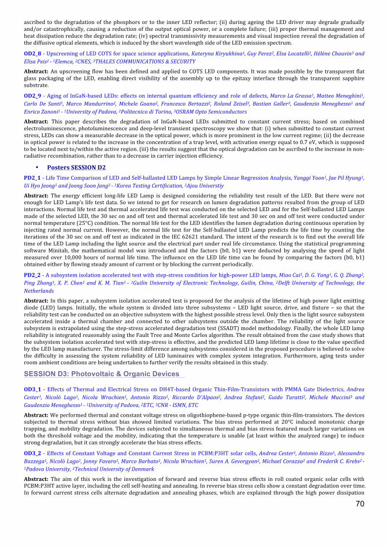
70
ascribed! to! the!degradation!of! the!phosphors!or! to! the! inner!LED!reflector;! (ii)!during!ageing! the!LED!driver!may!degrade!gradually!and/or!catastrophically,!causing!a!reduction!of! the!output!optical!power,!or!a!complete! failure;! (iii)!proper!thermal!management!and!heat!dissipation!reduce!the!degradation!rate;!(iv)!spectral!transmissivity!measurements!and!visual!inspection!reveal!the!degradation!of!the!diffusive!optical!elements,!which!is!induced!by!the!short!wavelength!side!of!the!LED!emission!spectrum.-
OD2_8!"!Upscreening!of!LED!COTS!for!space!science!applications,!Kateryna(Kiryukhina1,(Guy(Perez2,(Elsa(Locatelli2,(Hélène(Chauvin3(and(Elisa(Peis2(6(1Elemca,(2CNES,(3THALES(COMMUNICATIONS(&(SECURITY!Abstract:-An!upscreening! flow!has!been!defined!and!applied! to!COTS!LED!components.! It!was!made!possible!by! the! transparent! flat!glass! packaging! of! the! LED,! enabling! direct! visibility! of! the! assembly! up! to! the! epitaxy! interface! through! the! transparent! sapphire!substrate.-
OD2_9! "!Aging!of! InGaN"based!LEDs:!effects!on! internal!quantum!efficiency!and!role!of!defects,!Marco(La(Grassa1,(Matteo(Meneghini1,(Carlo( De( Santi1,( Marco(Mandurrino2,( Michele( Goano2,( Francesco( Bertazzi2,( Roland( Zeisel3,( Bastian( Galler3,( Gaudenzio(Meneghesso1( and(Enrico(Zanoni1(6(1University(of(Padova,(2Politecnico(di(Torino,(3OSRAM(Opto(Semiconductors!Abstract:- This! paper! describes! the! degradation! of! InGaN"based! LEDs! submitted! to! constant! current! stress;! based! on! combined!electroluminescence,!photoluminescence!and!deep"level!transient!spectroscopy!we!show!that:!(i)!when!submitted!to!constant!current!stress,!LEDs!can!show!a!measurable!decrease!in!the!optical!power,!which!is!more!prominent!in!the!low!current!regime;!(ii)!the!decrease!in!optical!power!is!related!to!the!increase!in!the!concentration!of!a!trap!level,!with!activation!energy!equal!to!0.7!eV,!which!is!supposed!to!be!located!next!to/within!the!active!region.!(iii)!the!results!suggest!that!the!optical!degradation!can!be!ascribed!to!the!increase!in!non"radiative!recombination,!rather!than!to!a!decrease!in!carrier!injection!efficiency.-
• Posters-SESSION-D2-PD2_1!"!Life!Time!Comparison!of!LED!and!Self"ballasted!LED!Lamps!by!Simple!Linear!Regression!Analysis,!Yanggi(Yoon1,(Jae(Pil(Hyung1,(Ui(Hyo(Jeong1(and(Joong(Soon(Jang2(6(1Korea(Testing(Certification,(2Ajou(Universtiy!
Abstract:- The! energy! efficient! long"life! LED! Lamp! is! designed! considering! the! reliability! test! result! of! the! LED.! But! there!were! not!enough!for!LED!Lamp’s!life!test!data.!So!we!intend!to!get!for!research!on!lumen!degradation!patterns!resulted!from!the!group!of!LED!interactions.!Normal!life!test!and!thermal!accelerated!life!test!was!conducted!on!the!selected!LED!and!for!the!Self"ballasted!LED!Lamps!made!of!the!selected!LED,!the!30!sec!on!and!off!test!and!thermal!accelerated!life!test!and!30!sec!on!and!off!test!were!conducted!under!normal!temperature!(25°C)!condition.!The!normal!life!test!for!the!LED!identifies!the!lumen!degradation!during!continuous!operation!by!injecting! rated! normal! current.! However,! the! normal! life! test! for! the! Self"ballasted! LED! Lamp! predicts! the! life! time! by! counting! the!iterations!of!the!30!sec!on!and!off!test!as!indicated!in!the!IEC!62621!standard.!The!intent!of!the!research!is!to!find!out!the!overall! life!time!of!the!LED!Lamp!including!the!light!source!and!the!electrical!part!under!real!life!circumstance.!Using!the!statistical!programming!software! Minitab,! the! mathematical! model! was! introduced! and! the! factors! (b0,! b1)! were! deducted! by! analysing! the! speed! of! light!measured!over!10,000!hours!of!normal! life! time.!The! influence!on! the!LED! life! time! can!be! found!by! comparing! the! factors! (b0,! b1)!obtained!either!by!flowing!steady!amount!of!current!or!by!blocking!the!current!periodically.-
PD2_2!"!A!subsystem!isolation!accelerated!test!with!step"stress!condition!for!high"power!LED!lamps,!Miao(Cai1,(D.(G.(Yang1,(G.(Q.(Zhang2,(Ping( Zhang1,( X.( P.( Chen1( and(K.(M.( Tian1(6( 1Guilin(University( of( Electronic( Technology,( Guilin,( China,( 2Delft(University( of( Technology,( the(Netherlands!Abstract:- In!this!paper,!a!subsystem!isolation!accelerated!test!is!proposed!for!the!analysis!of!the!lifetime!of!high!power!light!emitting!diode! (LED)! lamps.! Initially,! the!whole! system! is! divided! into! three! subsystems! –! LED! light! source,! drive,! and! fixture! –! so! that! the!reliability!test!can!be!conducted!on!an!objective!subsystem!with!the!highest!possible!stress!level.!Only!then!is!the!light!source!subsystem!accelerated! inside! a! thermal! chamber! and! connected! to! other! subsystems! outside! the! chamber.! The! reliability! of! the! light! source!subsystem!is!extrapolated!using!the!step"stress!accelerated!degradation!test!(SSADT)!model!methodology.!Finally,!the!whole!LED!lamp!reliability!is!integrated!reasonably!using!the!Fault!Tree!and!Monte!Carlos!algorithm.!The!result!obtained!from!the!case!study!shows!that!the!subsystem!isolation!accelerated!test!with!step"stress!is!effective,!and!the!predicted!LED!lamp!lifetime!is!close!to!the!value!specified!by!the!LED!lamp!manufacturer.!The!stress"limit!difference!among!subsystems!considered!in!the!proposed!procedure!is!believed!to!solve!the! difficulty! in! assessing! the! system! reliability! of! LED! luminaires!with! complex! system! integration.! Furthermore,! aging! tests! under!room!ambient!conditions!are!being!undertaken!to!further!verify!the!results!obtained!in!this!study.-
SESSION D3: Photovoltaic & Organic Devices
OD3_1! "! Effects! of! Thermal! and!Electrical! Stress! on!DH4T"based!Organic!Thin"Film"Transistors!with! PMMA!Gate!Dielectrics,!Andrea(Cester1,( Nicolò( Lago1,( Nicola( Wrachien1,( Antonio( Rizzo1,( Riccardo( D'Alpaos2,( Andrea( Stefani2,( Guido( Turatti2,( Michele( Muccini3( and(Gaudenzio(Meneghesso1(6(1University(of(Padova,(2ETC,(3CNR(6(ISMN,(ETC!
Abstract:-We!performed!thermal!and!constant!voltage!stress!on!oligothiophene"based!p"type!organic!thin"film"transistors.!The!devices!subjected! to! thermal! stress! without! bias! showed! limited! variations.! The! bias! stress! performed! at! 20°C! induced! monotonic! charge!trapping,!and!mobility!degradation.!The!devices!subjected!to!simultaneous!thermal!and!bias!stress!featured!much!larger!variations!on!both! the! threshold!voltage!and! the!mobility,! indicating! that! the! temperature! is!unable! (at! least!within! the!analyzed! range)! to! induce!strong!degradation,!but!it!can!strongly!accelerate!the!bias!stress!effects.-
OD3_2! "!Effects!of!Constant!Voltage!and!Constant!Current!Stress! in!PCBM:P3HT!solar!cells,!Andrea(Cester1,(Antonio(Rizzo1,(Alessandro(Bazzega1,(Nicolò(Lago1,(Jonny(Favaro1,(Marco(Barbato1,(Nicola(Wrachien1,(Suren(A.(Gevorgyan2,(Michael(Corazza2(and(Frederik(C.(Krebs2(6(1Padova(University,(2Technical(University(of(Denmark!
Abstract:- The! aim! of! this!work! is! the! investigation! of! forward! and! reverse! bias! stress! effects! in! roll! coated! organic! solar! cells!with!PCBM:P3HT!active!layer,!including!the!cell!self"heating!and!annealing.!In!reverse!bias!stress!cells!show!a!constant!degradation!over!time.!In! forward! current! stress! cells! alternate!degradation! and!annealing!phases,!which! are! explained! through! the!high!power!dissipation!
71
during!the!current!stress,!and!the!consequent!self"heating.!The!high!temperature!is!able!to!recover!the!cell!performances,!at!least!until!a!critical!temperature!is!reached.!Degradation!is!due!to:!the!decrease!of!the!net!generation!rate!(due!to!formation!of!exciton!quenching!centres!or!the!reduction!of!exciton!separation!rate);!the!formation!of!small!leaky!paths!between!anode!and!cathode,!which!reduces!the!total!current!extracted!from!the!cell.!The!stress"induced!damage!can!be!recovered!by!thermal!annealing!at!120°C.-
OD3_3!"!Case!study!of!failure!analysis!in!thin!film!silicon!solar!cell,!Domenico(Mello1,(Roberta(Ricciari1,(Anna(Battaglia2,(Marina(Foti1(and(Cosimo(Gerardi1(6(1STMicroelectronics,(23Sun!Abstract:-Thin"film!silicon!modules!are!commonly!produced!by!an!alternating!sequence!of!layer!deposition!and!layer!patterning!steps,!which! leads! to!a!monolithic! series! connected!device.!Most!used!process! is! laser! scribing!process! that!offers!a!high! throughput!and!a!small!area!loss.!Tin!oxide!(SnO2)!or!Zinc!oxide!(ZnO)!are!the!most!used!front!contact!TCO!in!the!superstrate!configuration.!ZnO!presents!better! optical! properties! with! respect! SnO2! and! can! be! realized! by! low! thermal! and! cost! effective! deposition! processes.! Electrical!performance!of!our!tandem!thin!film!silicon!cell!deposited!on!ZnO!front!contact!has!shown!higher!shunt!with!respect!with!our!reference!process!using!SnO2!front!contact,!not!explained!only!as!difference!between!the!two!materials.In!this!work,!a!failure!analysis!process!was!followed!in!order!to!explain!the!origin!of!the!difference.!SEM,!FIB!and!Auger!electron!spectroscopy!were!used!in!order!to!characterize!the!laser!scribe!that!is!known!to!be!a!possible!cause!of!electrical!deviation.!We!found!residuals!either!on!the!bottom!either!on!the!later!wall!of!P3!scribe!that!can!explain!the!lowering!shunt!resistance!and!open!circuit!voltage!observed!into!the!electrical!performances!of!the!module.-
• POSTER-SESSION-D3-PD3_1! "! Investigation!on!stress! induced!hump!phenomenon!in!IGZO!thin!film!transistors!under!negative!bias!stress!and!illumination,!Dae(Hyun(Kim1(and(Jong(Tae(Park2(6(1Incheon(national(University,(2University(of(Incheon!Abstract:-The!cause!of!the!stress!induced!hump!occurrence!in!IGZO!thin!film!transistor!has!been!investigated!through!experiment!and!device! simulation.! The! holes! accumulation! and! trapping! into! the! edge! region! under! negative! bias! stress! and! illumination! have! been!found!to!be!the!cause!of!the!hump!occurrence.!The!effects!of!the!quantity!of!the!holes!trapped!charges!and!the!length!of!the!edge!region!on!the!hump!occurrence!have!been!discussed.!From!the!device!simulation,! the!optimized!device!design!parameters,!such!as!the!IGZO!film!thickness!and!the!edge!length,!have!been!discussed!to!reduce!the!hump!occurrence!under!negative!bias!stress!and!illumination.-
PD3_2! "!The!degradation!mechanism!of! flexible!a"Si:H/μc"Si:H!photovoltaic!modules,! Jae6Seong(Jeong1(6(1Korea(Electronics(Technology(Institute((KETI)!
Abstract:-A! flexible!a"Si:H/μc"Si:H! tandem"junction!PV!module!was!produced,! in!which!a! thin! film!of!ZnO:B!grown!by!metal!organic!chemical!vapor!deposition!(MOCVD)served!as!the!TCO.!Its!stability!under!varying!environmental!stresses!was!assessed!by!a!reliability!test! based! on! the!MIL"STD"883G! standard,! revealing! that! its! efficiency! is! reduced! by! damp!heat! (85°C,! 85%! relative! humidity).! The!mechanism!behind!this!degradation!was!investigated!in!further!detail!by!assessing!the!ZnO:B!thin!film’s!reaction!to!moisture.!For!this,!flexible! a"Si:H/μc"Si:H! solar! cells! were! produced! with! deliberately! degraded! efficiencies! of! "20,! "50! and! "80%,! and! then! compared!against!similarly!degraded!ZnO:B!thin!films.!Amongst!the!various!electrical!parameters!measured,!both!Rs!and!the!short!circuit!current!(Isc)!exhibited!a!dramatic!increase!in!relation!to!the!extent!of!degradation,!whereas!Voc!showed!little!change.!Moreover,!the!decreasing!trend!of!efficiency!of!ZnO:B!was!found!to!correlate!to!its!Hall!mobility.!This!indicates!that!the!effect!of!moisture!is!to!increase!the!ZnO:B!layer’s! resistance,! thus! increasing! the! Rs! of! the! a"Si:H! PV.! Related! changes! in! the! physical! and! chemical! properties! of! ZnO:B! were!analyzed!by!XRD,!XPS!and!SIMS;!demonstrating!that!OH"!is!increased,!whereas!Zn2+!and!B3+!is!reduced!in!the!grain!boundaries!of!the!ZnO:B! surface.! Furthermore,! a! surface! reaction! occurs! between! hydroxide! and! Zn2+! ions! to! form! Zn(OH)2! at! the! grain! boundaries,!which!is!considered!to!be!an!important!aspect!of!the!observed!degradation!of!Rs!and!Isc.-
SESSION E1: Packaging & Assembly • SESSION&E1:&Defects&and&harsh&conditions!
OE1_1!"!A!Reliable!Solderless!Connection!Technique!for!high!I/O!counts!Ceramic!Land!Grid!Array!Package!for!Space!applications,!Jean6Baptiste( Sauveplane1,( Patrice(Retho2,(Norbert(Venet3,(Daniel(Buso1,(Guy(Perez1( and( Jean6Sébastien(Lefrileux2(6( 1CNES,( 2Hypertac,( 3Thales(Alenia(Space!
Abstract:-Area!Array!microelectronic!package!with!small!pitch!and! large! I/O!counts! is!now!widely!used! in! the!ceramic!packaging!of!microelectronics!Integrated!Circuit!(IC).!This!kind!of!Land!Grid!Array!(LGA)!device!cannot!be!directly!soldered!on!Printed!Circuit!Board!(PCB).!In!order!to!mount!them!on!PCB!the!LGA!device!back!end!is!mostly!terminated!with!solder!Columns!(CGA!device)!or!with!solder!Balls! (BGA!device).!For! space!application!CGA!and!BGA!ceramic!devices!are!prone! to!early! failure!due! to!harsh!environment.! Indeed!vibration!and!shock!during!launch!as!well!as!thermal!cycling!in!orbit!induces!a!high!level!of!stress!in!the!solder!joints!between!board!and!device.!Such!high!level!of!stress!can!ultimately!cause!the!failure!of!one!of!the!solder!joints!causing!permanent!functional!electrical!failure.!As!the!trend!for!next!generation!of!ceramic!ICs!device!is!to!increase!their!sizes!and!their!density!of!I/O,!susceptibility!to!mechanical!and!thermal!loading!grows!even!more.!This!statement!is!in!contradiction!with!the!high!level!of!reliability!required!for!space!application.!To!overcome!this!situation!CNES!has!taken!the!lead!with!space!users!and!space!connector!manufacturers!to!develop!for!space!application!a!reliable!solderless!solution!that!will!enable! to!easily!mount!on!board!the!actual!and!the!next!generation!of!ceramic! ICs!package.!This!solderless!solution!consists!in!using!a!thin!connector!interposer!between!the!ceramic!LGA!device!and!the!board.!A!clamping!system!is!used!to!hold!and!keep!aligned!on!the!board!the!stacking!composed!of!the!ceramic!device!and!the!interposer!connector.!This!solderless!solution!has!been!evaluated!according!to!the!European!space!standard!and!has!demonstrated!a!high!robustness!to!harsh!environment!making!this!solution!compliant!for!space!application.-
OE1_2! "! Impact( of( aluminum(wire( and( ribbon( bonding( technologies( on(D2PAK( package( reliability( during( thermal( cycling( applications,(Sébastien(Jacques1,(Rene(Leroy2(and(Marc(Lethiecq1(6(1GREMAN(CNRS6UMR(7347,(University(of(Tours,(2LMR(EA(2640,(University(of(Tours!
Abstract:-This!paper!highlights!the!impact!of!bonding!techniques!(Al!wire!and!Al!ribbon)!on!the!aging!of!Schottky!diodes,!assembled!in!D2PAK! package,! subjected! to! temperature! cycling.! The! experimental! test! results! coupled! with! failure! analysis! exhibit! a! better!

72
robustness!and!a!lifetime!about!2.3!higher!for!the!ribbon!bonding!assembly.!A!higher!contact!surface,!the!low!loop!profile!and!stiffness!for!ribbons!allow!slowing!down!crack!initiation!and!propagation!between!the!Al!bond!and!Al!metallization!on!the!top!of!the!silicon!die.-
OE1_3! "! Unusual! defects,! generated!by!wafer! sawing:! an! update,! including!pick&place! processing,!Peter( Jacob1(6( 1Empa(Swiss(Federal(Laboratories(for(Materials(Testing(and(Research!Abstract:-At!ESREF!2008,!the!paper!“Unusual!defects,!generated!by!wafer!sawing:!Diagnosis,!mechanisms!and!how!to!distinguish!from!related! failures”!had!won! the!Best!Paper!Award.! In! the!meantime,! new!experiences!were! collected,! related! to!new!methods! as! laser!stealth!dicing! and! its! specific!ESD! risks! and!additional! failure!mechanisms!as!backside!damage,! charging!of! foils! and! sawing! residue!damages.!This!paper!explains!in!detail!these!failure!sources,!including!detailed!explanations!on!root!causes!and!physical!mechanisms!as!well!as!important!hints!for!failure!analysts!how!to!distinguish!related!failure!signatures!from!those,!which!look!similar!but!are!of!other!origin.!As!a!real!update!to!the!paper!of!2008,!only!really!new!failure!mechanisms!and!new!knowledge!are!published!in!this!"updating"!paper.-
• SESSION&E1:&Fatigue&and&modeling!
OE1_4! "!Dynamical! IMC"Growth!Calculation,!Lutz(Meinshausen1,(Kirsten(Weide6Zaage2(and(Helene(Fremont3(6(1IMS(University(Hannover,(2RESRI(Group(IMS6AS(Uni(Hannover,(3IMS(University(Bordeaux!
Abstract:-Material!movement!between!solder! joints!and! their!contact!pads! leads! to! the! formation!of! intermetallic! compounds!at! the!contact!surfaces.!Concentration!gradients!are!responsible!for!this!material!movement.!The!intermetallic!compound!growth!in!12x12mm!Amkor®!SAC305!ball!grid!array!PoP!packages!including!direct!SAC"Cu!contacts!at!their!bottom!bumps!was!investigated.!Based!on!the!resulting! IMC! thickness! from!measurements! the! average!mass! flux!of!Cu! and!Sn!was! calculated.!Based!on! the!determined!activation!energies!(EA)!and!the!diffusion!constants!(D0)!from!measurements!the!migration!due!to!concentration!gradients!were!determined!by!a!routine!for!the!dynamical!calculation!of!IMC"growth!migration!effects.!These!calculations!are!validated!by!measurements-
OE1_5!"!Metal!fatigue!in!copper!pillar!Flip!Chip!BGA:!a!refined!acceleration!model!for!the!aluminium!pad!cracking!failure!mode,!Riccardo(Enrici(Vaion1,(Ruggero(Alberti1,(Alberto(Mervic1(and(Stefano(Testa2(6(1STMicroelectronics,(2Stmicroelectronics!
Abstract:-The!increasing!complexity!of!ASIC!pushed!the!industry!to!innovative!packaging!solutions!that!are!very!challenging!versus!high!automotive! quality! targets.! This! study! is! related! to! the! characterization! of! an! advanced! Flip! Chip! BGA! package! with! copper! pillar!interconnection!and!its!reliability!performance!during!temperature!cycle!stress!test!(aligned!to!AEC"Q100!Grade!1!perimeter![1]).-
• SESSION&E1:&Prototyping&and&analytic&tools!OE1_6!"!Intrinsic!Stress!Analysis!of!Tungsten"Lined!Open!TSVs,!Lado(Filipovic1,(Anderson(Pires(Singulani2,(Frederic(Roger2,(Sara(Carniello2(and(Siegfried(Selberherr1(6(1Institute(for(Microelectronics,(Technische(Universität(Wien,(2ams(AG!
Abstract:-The!effects!of!silicon!etching!and!subsequent!metallization!during! the! fabrication!of! tungsten"lined!open!TSVs! is!examined!using! a! combination! of! measurements! and! simulations.! The! total! stress! through! a! deposited! tungsten! film! is! measured! and! finite!element!simulations!are!performed!in!order!to!separate!the!intrinsic!and!thermal!stress!components!in!the!film.!The!data!is!then!used!to!observe!and!model! the!stress!through!a!TSV!structure,!which! is!etched!using!the!DRIE!process,!resulting! in!scalloped! inner!sidewalls!through!the!TSV!opening.!The!scalloped!structure! is! then!compared!to!the! ideal! flat!alternative!with!regard!to!the!stress! through!the!metal!film!and!the!TSV's!electrical!parameters,!including!resistance,!capacitance,!and!inductance.!It!is!found!that!the!stress!around!the!scallop!varies!significantly,!but!that!the!average!stress!through!the!tungsten!in!the!flat!TSV!is!not!very!different!from!the!scalloped!TSV.!However,!the!resistance,!capacitance,!and!inductance!are!found!to!increase!in!the!presence!of!scallops.-
OE1_7! "! Virtual! prototyping! in! a! Design"for"Reliability! approach,! Samed( Barnat1,( Alexandrine( Guédon6Gracia2( and( Helene( Fremont2(6(1ISEFC,(Université(virtuelle(de(Tunis,(Tunisie,(2IMS6Bordeaux!
Abstract:-The!main!purpose!of!the!paper!is!to!present!a!methodological!approach!combining!experiments!and!simulations!for!virtual!prototyping!in!a!Design"for"Reliability!approach.!Two!examples!illustrate!the!methodology!and!the!importance!of!a!wise!choice!of!the!adequate!failure!criterion!for!numerical!modelling.!In!the!first!example,!the!stress!induced!in!silicon!is!axial!whereas!it!is!radial!in!the!second!case.!Strength!data!recorded!from!three"point"bend!tests!have!been!regarded!in!the!first!case,!whereas!in!the!second!case,!ball"on"ring!test!results!have!been!considered.!
• POSTERS-SESSION-E1-PE1_1! "!Correlation!between!mechanical!properties!and!microstructure!of!different!aluminum!wire!qualities!after!ultrasonic!bonding,!Marian( Sebastian( Broll1,( Ute( Geissler1,( Jan( Höfer2,( Stefan( Schmitz2,( Olaf(Wittler2,( Martin( Schneider6Ramelow2( and( Klaus( Dieter( Lang1( 6(1Technische(Universität(Berlin,(2Fraunhofer(IZM!
Abstract:-Three!different!heavy!aluminum!wire!qualities!were! investigated!regarding!their!microstructural!evolution!after!ultrasonic!bonding!by!electron!backscatter!diffraction!and!nanoindentation.!The!results!complete!the!findings!of!our!recent!research!regarding!the!effect! of! bonding! mechanisms! on! the! wire! bond! microstructure! and! its! local! mechanical! properties.! Local! elastic"plastic! material!parameters!of!the!bonded!wires!were!approximated!on!the!basis!of!the!elastic!anisotropy!of!crystals!and!a!correlation!between!hardness!and!stress.-
PE1_2!"!Thermal!cycle!reliability!of!Cu!nanoparticle!joint,!Toshitaka(Ishizaki1,(Masanori(Usui1(and(Yasushi(Yamada2(6(1Toyota(Central(R&D(Labs.,(Inc.,(2Daido(University!Abstract:-Thermal!cycle!tests!of!"40/150!ºC!and!"40/200!ºC!were!carried!out!on!joint!samples!by!Cu!nanoparticles!and!Sn"0.7!wt.!%Cu!solder.!The!sample!joined!by!Cu!nanoparticles!at!300!ºC!was!not!damaged!after!"40/150!ºC,!but!completely!broken!in!the!joint!interface!after!"40/200!ºC!thermal!cycle.!The!joint!interface!was!strengthened!as!the!joint!temperature!was!increased!to!be!350!ºC!so!that!the!Cu!nanoparticle!joint!could!endure!"40/200!ºC!thermal!cycle.!The!soldered!joint!was!completely!broken!in!the!joint!layer!after!"40/200!ºC!thermal!cycle.-

73
PE1_3! "! Online! test!method! of! FPGA! solder! joint! resistance!with! low! power! consumption,!Nantian(Wang1,(Yue(Li1,( Zongyue(Yu1(and(Zhiqian(Ren1(6(1Science(and(Technology(on(Integrated(Logistics(Support(Laboratory,(National(University(of(Defense(Technology!Abstract:-Solder! joint!resistance!monitoring! is! important! to!electronic!system!PHM.!The!traditional!built"in!self"test!method!of!FPGA!solder! joint! based! on! charging! and! discharging! of! single! capacitance! shows! the! shortcoming! of! large! power! consumption! and!unavailability!of!the!monitored!pins!in!FPGA's!functional!design.!In!this!paper,!we!propose!an!online!measuring!method!of!FPGA!solder!joint! resistance! with! low! power! consumption! aiming! at! the! application! with! limited! pins! and! power.! The! model! of! the! method! is!introduced,!including!external!test!circuit,!internal!test!IP!core!and!parameter!determination.!Its!power!consumption!is!analysed.!Based!on!a!Xilinx!Spartan!6!FPGA,!a!platform!is!built,!and!experiments!are!conducted.!Results!show!that!the!method!can!successfully!measure!the!resistance!of!the!solder!joint!of!FPGA's!in!application!output!pins!with!lower!power!consumption!than!the!traditional!built"in!self"test!method.-
PE1_4-"!Moisture!Absorption!and!Desorption!in!Wafer!Level!Chip!Scale!Packages,!Kirsten(Rongen1,(Amar(Mavinkurve1,(Matt(Chen1,(Frank(Swartjes1,(Paul(van(der(Wel1(and(Rene(Rongen1(6(1NXP(Semiconductors!
Abstract:- Life! test! standards! for! qualification! like! JEDEC! have! been! set"up! for! traditional! lead! frame! or! substrate! based! packages.!Among!others,!it!is!stated!in!the!well"known!JEDEC!standard!for!preconditioning,!that!a!soaking!step!before!reflowing!is!mandatory!for!the!release!of!SMD!devices,!which!are!sensitive!to!absorb!moisture.-
PE1_5!"!A!numerical!procedure!for!simulating!thermal!oxidation!diffusion!of!epoxy!molding!compounds,!Zaifu(Cui1,(Daoguo(Yang2(and(Miao(Cai2(6(1Luzhou(Vocational(&(Technical(College,(2Guilin(University(of(Electronic(Technology!Abstract:- A! new! numerical! approach! is! developed! for! simulating! thermal! oxidation! diffusion! of! epoxy!molding! compounds.! In! this!approach,! we! utilize! the! formal! similarity! of! oxidation! diffusion! equation! and! heat! conduction! equation! to! convert! the! oxidation!diffusion!issue!into!heat!conduction!issue,!then!a!two"dimensional!finite!element!model!of!epoxy!molding!compounds!is!established,!and!by! using! ANSYS! thermal! conduction!modules,! oxidation! diffusion! issues! of! epoxy!molding! compounds! aged! under! 150! ºC! is! solved.!Comparison!of!the!results!of!the!method!and!documentation!indicates!that!by!using!this!approach!oxidation!diffusion!of!epoxy!molding!compounds!can!be!simulated,!which!provides!a!method!for!solving!issues!of!thermal!oxidation!of!epoxy!molding!compounds.-
PE1_6!"!Effect!of!Thermal!Aging!on!the!Electrical!Resistivity!of!Fe"added!SAC105!Solder!Alloys,!Mohd(Faizul(Mohd(Sabri1,(Suhana(Mohd(Said1,(Nur(Aishah(Aminah(Mohd(Amin1,(Hamzah(Arof1(and(Iswadi(Jauhari1(6(1University(of(Malaya!Abstract:-SAC!105!solders!doped!with!a!minor!addition!of!Fe!(include!wt%)!have!been!shown!to!demonstrate!excellent!thermal!cyclic!reliability.! To! complement! the! mechanical! performance,! the! electrical! resistivities! of! SAC105,! SAC105"0.1Fe,! SAC105"0.3Fe,! and!SAC105"0.5Fe!bulk!solder!alloys!were!also!characterised!after! thermal!aging!performance.!Results!showed!that! the!overall! resistivity!decreased!after!thermal!aging.!However,!no!specific!trend!were!identified!for!every!changes!in!each!type!of!solder!alloy.!The!electrical!resistivity!of!the!undoped!SAC105!solder!alloy!decreased!for!as!much!as!13%!after!the!thermal!aging!process.!Meanwhile!the!electrical!resistivity!for!0.1wt.%,!0.3wt.%,!and!0.5wt.%!Fe"bearing!SAC105!solder!alloys!decreased!at!25%,!11%,!and!17%!respectively,!showing!a!rather!stable!reduction!in!resistivity,!which!can!be!correlated!to!the!microstructure!of!the!Fe"added!SAC!105!after!thermal!aging.-
PE1_7! "!The!Effect!of! Iron!and!Bismuth!addition!on! the!Microstructural,!Mechanical,!and!Thermal!Properties!of!Sn–1Ag"0.5Cu!Solder!Alloy,!Mohammad(Hossein(Mahdavifard1,(Mohd(Faizul(Mohd(Sabri1,(Dhafer(Abdulameer(Shnawah1,(Irfan(Anjum(Badruddin1,(Shaifulazuar(Rozali1(and(Suhana(Mohd(Said1(6(1University(of(Malaya!Abstract:-This!work!investigates!the!effect!of!Fe!and!Bi!addition,!0.05%!Fe!and!1%!or!2%!Bi,!on!the!microstructural,!mechanical,!and!thermal! properties! of! the! Sn–1Ag"0.5Cu! (SAC105)! solder! alloy.! Adding! Bi! and! Fe! to! SAC105! increased! UTS! and! yield! strength! and!decreased! the! total! elongation! which! is! related! to! solid"solution! and! precipitation! strengthening! effects! by! Bi! in! the! Sn"rich! phase.!Scanning!electron!microscopy!(FESEM)!and!EDX!showed!that!by!adding!Bi!to!SAC105"Fe,!it!is!scattered!in!the!bulk!of!the!solder,!thereby!increasing!β"Sn!and!degenerated!Cu6Sn5!and!Ag3Sn!into!a!chain"like!arrangement.!Thus,!the!addition!of!Fe!and!Bi!to!SAC105!decreased!the!alloy’s!solidus!temperature!by!5°C!and!increased!its!pasty!range!by!4°C.-
SESSION E2: MEMS, MOEMS, NEMS & Nano-objects OE2_1! "! Dielectric! charging! effects! in! floating! electrode! MEMS! capacitive! switches,! Loukas( Michalas1,( Matroni( Koutsoureli1,( Eleni(Papandreou1,(Flavio(Giacomozzi2(and(George(Papaioannou1(6(1UOA,(2FBK!Abstract:-The!paper!presents! a! study!oriented! to! the!understanding!of! the! floating! electrode! role! on! the! charging! characteristics! of!floating!electrode!RF!MEMS!capacitive!switches.!Identical!devices!with!and!without!floating!electrode!have!been!stressed!under!induced!charging!mode.!Biases!of!different!levels!and!polarities!were!applied!to!the!transmission!line.!Reduced!and!asymmetric,!respect!to!the!bias! polarity,! charging! effects! were! obtained! on! devices! with! floating! electrode! compared! to! the! conventional! ones.! The! results!contribute!towards!the!conclusion!that!the!use!of!floating!electrode!in!conjunction!with!the!appropriate!actuation!polarity!may!reduce!the!charging!effects!and!thus!to!improve!the!device!lifetime.-
OE2_2! "! Robust! design! of! thermo"mechanical! MEMS! switch! embedded! in! aluminium! BEOL! interconnect,! Sebastian( Orellana1,( Brice(Arrazat2,(Pascal(Fornara3,(Christian(Rivero3,(Sylvain(Blayac2,(Pierre(Montmitonnet4(and(Karim(Inal4(6(1Mines6Paristech(/(STMicroelectronics,(2Ecole(Nationale(Supérieure(des(Mines(de(Saint6Etienne,(CMP,(3STMicroelectronics,(4Mines(ParisTech,(CEMEF!Abstract:-A!new!concept!of!a!thermo"mechanical! lateral!switch!activation!is!proposed.!Embedded!in!standard!aluminum!BEOL!(Back!end!of!the!line),!it!is!fully!integrated!in!CMOS!technology.!The!simplicity!of!this!low!cost!one"mask!fabrication!allows!the!straightforward!scalability!of!design.!Most!functional!problems!have!been!solved!through!process,!simulation!and!design:!stiction,!bending,!displacement,!robustness.!However,! apparent! surface! contact! of! 0.2! µm2,! temperature! variations! undergone! by! the! device! in! its! life! and! surety! of!symmetrical! activation! are! potential! failure! sources.! Novel! designs! are! proposed! to! overcome! these! failure! sources! together!with! a!running"in!step!before!operation.-
OE2_3!"!Failure!mechanisms!of!microbolometer!thermal!imager!sensors!using!chip"scale!packaging,!Michael(Elßner1(61Fraunhofer(IMS(!

74
Abstract:-This!paper!analyses!relevant!failure!mechanisms!for!microbolometer!thermal!imager!sensors!that!are!assembled!with!a!small!size!and!low!cost!chip!scale!package.!The!analyses!focus!at!device!specific!elements!like!the!bolometer!sensor!structures,!the!longtime!stability!of!the!sensor!and!its!performance,!and!the!stability!of!the!hermetic!chip!scale!package.!Executed!reliability!tests!showed!a!high!reliability!of!the!sensor!and!the!package!without!hard!failures.!The!package!survived!harsh!environmental!accelerated!stress!tests!and!showed! only! a! slight! reduction! of! the! shear! strength! through! void! formation! and! small! cracks!within! the! lead! frame! that! could! be!verified! through! FEM! simulations.! The! stress! on! the! bolometers! is! investigated! by! thermomechanical! FEM! simulations.! Executed!reliability!tests!showed!no!enlargement!in!the!number!of!defect!pixel.!The!sensor!performance!showed!a!longtime!drift!and!temperature!dependence! through!outgassing!processes! inside! the!package! leading! to!a!performance!reduction!of!nearly!10%!after!one!year.!Thus!this!effect!is!investigated!closer!and!possible!countermeasures!are!proposed.-
OE2_4!"!Reliability!test!of!a!RF!MEMS!varactor!based!on!a!double!actuation!mechanism,!Alessandro(Cazzorla1,(Paola(Farinelli2,(Roberto(Sorrentino1(and(Benno(Margesin3(6(1Department(of(Engineering,(University(of(Perugia,(2RF(Microtech,(3Fondazione(Bruno(Kessler((FBK)!
Abstract:-This!paper!presents!the!design!and!reliability!tests!of!a!novel!micro"electro!mechanical!varactor!based!on!a!double!actuation!mechanism!allowing! for!overall! capacitive! ratio!Cr!of!5.2!and!continuous!capacitive! ratio!Cr*!of!2.6.!The!device!has!been!modeled! in!ANSYS®!multiphysics!environment!and!manufactured!by!using!the!8"masks!FBK"irst!RF!MEMS!process.!The!performance!was!tested!on!10! samples! showing! good!mechanical! reproducibility! and! negligible! capacitance! ratios! variation! (Cr=5.2! ±! 5%,! Cr*=2.6! ±! 3%).! Self"biasing!tests!have!been!performed!by!applying!an!equivalent!Vrms!on!the!RF!central!conductor,!showing!an! insignificant!capacitance!ratio!variation!up!to!13.5Vrms.!Finally,!cycling!test!was!performed!on!the!DUT!up!to!100!million!cycles,!showing!negligible!variation!of!the!capacitance.!Self"heating!tests!are!on"going.-
• POSTERS-SESSION-E2-PE2_1! "! Induced! charging! phenomena! on! SiNx! dielectric! films! used! in! RF! MEMS! capacitive! switches,!Matroni( Koutsoureli1,( Loukas(Michalas1,(Eleni(Papandreou1(and(George(Papaioannou1(6(1University(of(Athens!Abstract:- Contact"less! charging! process! has! been! found! to! constitute! a! compensation! mechanism! to! dielectric! charging! of! MEMS!capacitive!switches.!The!present!paper!aims!to!provide!a!better!knowledge!of!induced!charging!mechanisms!that!appear!in!HF!PECVD!silicon!nitride! films.!The!characteristics!of! this!process!as!well!as! the!degree!of! compensation!are! investigated! for!different! stressing!field!intensities!of!both!polarities!in!MEMS!capacitive!switches.!The!experimental!results!indicate!that!the!degree!of!compensation!in!HF!PECVD!SiNx!films!seems!to!increase!with!the!intensity!of!the!applied!electric!field!and!it!is!also!affected!by!the!polarity!of!the!stressing!bias.-
PE2_2! "!A!way! to! implement! the!Electro"Optical! technique! to! inertial!MEMS,!Kevin(Melendez1,(Kevin(Sanchez1,(Philippe(Perdu1,(Adrien(Desmoulin2(and(Dean(Lewis3(6(1CNES,(2ELMCA,(3University(of(bordeaux!
Abstract:-This!paper!descripts!a!new!way!to!analyses!inertial!MEMS!with!the!electro"optical!technique.!Usually,!this!technique!is!used!in!the!failure!analysis!to!probe!on!electronic!devices!from!old!technologies!to!modern!VLSI.!In!our!case,!we!use!the!power’s!variation!of!the!reflected!beam!with!materials! layer! in! an!accelerometer! (MEMS).!We! introduce!a!new!method!based!on!electro"optical! technique! to!extract!a!physical!resonant!frequency!in!inertial!MEMS.-
PE2_3! "! Reliability! of! platinum! electrodes! and! heating! elements! fabricated! on! SiO2("covered)! substrates! and!membranes,!Radoslav(Rusanov1,(Holger(Rank1,(Juergen(Graf1,(Tino(Fuchs1,(Roland(Mueller6Fiedler1(and(Oliver(Kraft2(6(1Robert(Bosch(GmbH,(2Institute(for(Applied(Materials,(Karlsruhe(Institute(of(Technology!
Abstract:-In!this!work,!a!method!for!the!determination!of!thermal!conductivity!and!thermal!capacitance!of!thin!insulating!films!has!been!adapted! for! the! characterization! of! PECVD! silicon! oxide! and! successfully! applied! on! two!materials!with! different! deposition! recipes.!These!two!materials!are!used!for!the!fabrication!of!platinum!heating!elements!with!PECVD!SiO2!as!insulation"!or!membrane"layer.!The!results!for!the!two!recipes!are!similar!but!with!a!measurable!difference.!A!slight!increase!of!the!conductivities!has!been!observed!due!to!a!thermal!anneal!of!the!test!structures!at!temperatures!above!700°C.!Failure!mechanisms!as!adhesion!problems,!material!migration!due!to! thermally! induced! compressive! stress! and! electromigration! that! could! occur! in! the! platinum! electrodes! and! heater! structures! at!temperatures!above!600°C!have!been!also!systematically!studied!in!this!work.!Lifetime!determination!and!optical!and!scanning!electron!microscopy! have! been! applied! for! samples! which! have! experienced! different! loading! conditions! to! understand! qualitatively! and!quantitatively!the!phenomena.!The!aim!is!to!enable!time"to"failure!prediction!and!thus!provide!guidelines!for!limiting!temperature!and!current!density!in!a!heating!structure!to!ensure!its!stability!over!lifetime.!We!use!dedicated,!application"related!test!structures!to!ensure!that!the!results!are!applicable!to!sensor!lifetime!estimations.-
PE2_4! "! Charge! induced! by! ionizing! radiation! understood! as! a! disturbance! in! a! sliding! mode! control! of! dielectric! charge,!Manuel(Dominguez6Pumar1,(Sergi(Gorreta1,( Joan(Pons6Nin1,(Faustino(Gomez6Rodriguez2(and(Diego(M(Gonzalez6Castaño2(6(1Universitat(Politecnica(de(Catalunya,(2Universidade(de(Santiago(de(Compostela!Abstract:-The!purpose!of! this!paper! is! to!show!that!the!charge! induced!by!radiation! in!a!dielectric!on!which!a!sigma"delta!control!of!dielectric! charge! is! implemented,! can! be! seen! as! a! disturbance! in! a! sliding! mode! controller.! Preliminary! experimental! results! are!presented!on!which!a!MEMS!device!is!irradiated!with!X"rays,!while!the!dielectric!charge!control!is!continuously!being!monitored.!The!charge!induced!by!radiation!generates!a!change!in!the!control!bitstream,!which!is!associated!to!the!presence!of!an!external!disturbance!on!the!governing!control!equations.-
SESSION F: Power devices • SESSION&F:&Power&modules!
OF_1! "! A! thermal! modeling! methodology! for! power! semiconductor! modules,! Christoph( van( der( Broeck1,(Marcus( Conrad1( and( Rik(De(Doncker1(6(1Institute(for(Power(Electronics(and(Electrical(Drives,(RWTH(Aachen(University!Abstract:-It!is!the!objective!of!this!work!to!present!flexible!thermal!modeling!methodology!for!power!semiconductor!modules!allowing!time!efficient!simulation!of!temperature!cycling!for!different!module!designs!and!operation!strategies.!To!keep!the!model!compact!and!

75
flexible!as!well!as!accurate,!the!solid!state!heat!conduction!paths!of!the!power!modules!are!modeled!by!a!3D!finite!difference!model.!It!is!combined!with!an!analytical!heat!sink!model!of!the!convection!process.!The!temperature!gradient!of!the!cooling!fluid!is!captured!by!a!mass!transportation!model.!The!resulting!linear!state!space!model!can!be!easily!formulated!in!discrete!time!domain!to!allow!a!fast!and!detailed! simulation! of! thermal! load! transients.!With! the! Hankel"Singular"Value! based!model! reduction! technique,! the! thermal! state!space!model! can! be! further! reduced! to! allow! fast! analysis! of! thermal! cycling! and! reliability.! For! the! performance! evaluation! of! the!modeling!approach!the!thermal!model!is!compared!with!experimental!results!and!data!from!the!manufacture.-
OF_2! "!Ageing!monitoring! in! IGBT!module!under! sinusoidal! loading,!Pramod(Ghimire1,(Kristian(Bonderup(Pedersen1,(Bjørn(Rannestad2(and(Stig(Munk6Nielsen1(6(1Aalborg(University,(2KK(Wind(Solutions(a/s!
Abstract:- This! paper! presents! monitoring! of! ageing! in! high! power! Insulated! Gate! Bipolar! Transistor! (IGBT)! modules! subjected! as!sinusoidal!loading.!On"state!collector"emitter!voltage!uce_on!for!IGBT,!forward!voltage!for!diode,!and!rise!in!interconnection!re"!sistance!are!used!as!ageing!parameters.!These!are!measured!in!three!different!ways:!calibration!of!power!modules!after!24!h!of!operation,!offline!characterization!every!5!min!of!operation,!and!continuous!measurement!during!normal!converter!operation.!Four!power!modules!are!tested,!which!are!cycled!to!different!degradation! levels!by!number!of!cycles,!where!one! is! tested!until! failure.!The!characterization!at!different!stages!of! lifetime!indicates!that!the!rise! in!resistance!originates!from!thermo"mechanical!degradation!of! interconnects.!Post"test! investigations:! four"point! probing! and! micro"sectioning! indicate! thermo"mechanical! induced! degradation! of! the! chip! topside!interconnects! as! the! source! for! rise! in! resistance.!Major! degradations! are! observed! in! bond!wires! and!metallization! on! the! low! side!diode.!!
OF_3! "! Robustness! of! MW"Level! IGBT! Modules! against! Gate! Oscillations! under! Short! Circuit! Events,! Paula( Diaz( Reigosa1,( Rui(Wu1,(Francesco(Iannuzzo1(and(Frede(Blaabjerg1(6(1Aalborg(University!Abstract:-The!susceptibility!of!MW"level!IGBT!power!modules!to!critical!gate!voltage!oscillations!during!short!circuit!events!has!been!evidenced! experimentally.! This! abstract! proposes! a! sensitivity! analysis! method! to! better! under"stand! the! oscillating! behaviour!dependence! on!different! operating! conditions! (i.e.,! collector"emitter! voltage,! gate"emitter! voltage! and! temperature).! A! study! case! on!several!repetitive!short!circuits!of!1.7!kV/!1!kA!IGBT!power!modules!demonstrates!the!procedure!and!the!results!of!the!analysis.!The!proposed! study! helps! for! understanding! the! oscillation!mechanism! by! revealing! its! relationship!with! different! operating! conditions.!Moreover,!it!is!possi"ble!to!select!a!safe!operating!margin!of!the!device!to!avoid!lack!of!robustness!against!gate!voltage!oscillations!and!further!improve!the!device!performance!under!short!circuits.-
OF_4! "! Preliminary! failure"mode! characterization! of! emerging!Direct"Lead"Bonding! power!module.! Comparison!with! standard!wire"bonding! interconnection,! William( Sanfins1,( Damien( Risaletto1,( Frédéric( Richardeau1,( Gaël( Blondel2,( Michaël( Chemin2( and( Philippe(Baudesson2(6(1LAPLACE,(2VALEO!Abstract:-The!Direct"lead"bonding!interconnection!appears!to!be!a!promising!technology!for!power"module.!Nevertheless,!the!absence!of!wire"fuse"effect! in!case!of!extreme! failure,! compared! to!classical!wire"bonding,! leads!authors! to!rethink! fail"safe!and! fault"tolerant!strategies! for! critical! converter.! Therefore,! this! paper! will! provide! a! comparative! approach! between! these! two! designs! in! terms! of!failure"mode! and! post"fault! high"current! capability! of! a! dual"chip! power"module.! Thanks! to! a! controlled! energy! source,! chips! are!destroyed! for! different! amount! of! energy! and! the! fault! residual! resistance! obtained! is! thermally! stressed! through! high! continuous!current.!Finally,!non"destructive!defect!localization!with!Lock"in!thermography!coupled!to!RX!tomography!is!performed!to!thoroughly!analyze!the!defect!area.-
OF_5! "! Identification! and! analysis! of! power! substrates! degradations! subjected! to! severe! ageing! tests,! Eric(Woirgard1,( Faical( Arabi1,(Wissam(Sabbah1,(Donatien(Martineau2,(Loic(Theolier1(and(Stephane(Azzopardi3(6(1IMS(University(of(Bordeaux,(2Labinal(Power(System,(3IMS(Laboratory!Abstract:- Severe! thermal! cycling! range! ["55°C/+245°C]! have! highlighted! degradations! in! power! substrates! AMB! Si3N4!with! copper!metallization,!nickel!plated!and!gold!finish.!After!2,000!thermal!cycles,!the!metallization!patterns!of!the!topside!were!imprinted!on!the!rear! one! due! to!microcracking! of! the! rear! surface!metallization! and! the! surface! roughness!modification.! This! phenomenon!was! not!observed! in! less! severe! thermal! cycling! as! ["40°C/+150°C].! This! study! focuses! on! the! causes! of! this! degradation! appearance! and! on!remedial!means.! First,! the! power! electronics! context! is! presented! to! justify! the! severe! stresses! applied! to! high! temperature! power!modules!and!then!induced!degradations!were!described!and!analyzed.!The!choice!was!to!perform!a!protocol!of!ageing!process!by!finite!element!simulations! in!order!to!have!a!better!understanding!on!the!propagation!of!mechanical!stresses! in!the!substrate,!which! is! the!origin!of!these!degradations.!Indeed,!this!phenomenon!could!be!reproduced!by!thermomechanical!simulations.!To!propose!solutions!for!these! crippling! degradations,! the! effect! of! the! copper!metallization! thickness,! the! coefficient! of! thermal! expansion! of! this! layer,! the!substrate!warpage!and!the!size!of!metallization!bonding!tracks!was!assessed.!The!objective!is!to!offer!technological!choices!in!term!of!geometry!of!metallization!tracks!bonding!(minimal!etching!or!traditional!engraving)!and!choices!of!materials!used!in!power!substrates!in!order!to!avoid!these!degradations!in!extreme!environment!conditions.-
• SESSION&F:&Power&devices!OF_6! "! In"depth!investigation!of!metallization!aging! in!power!MOSFETs! ,!Roberta(Ruffilli1,(Mounira(Berkani2,(Philippe(Dupuy3,(Stephane(Lefebvre2,( Yann( Weber3( and( Marc( Legros1( 6( 1CEMES6CNRS,( Freescale( Semiconducteur,( 2Laboratoire( SATIE,( ENS6Cachan,( 3Freescale(Semiconducteur!
Abstract:-The!long"term!reliability!of!modern!power!MOSFETs!is!assessed!through!two!types!of!electro"thermal!aging!tests!(avalanche!and! short"circuit).! Previous! studies! have! shown! that! the! source!metallization! (top!metal! and!wires)! is! a! location! of! the! component!where! failure! is! prone! to! happen.! To! study! how! the! top! Aluminum!metallization!microstructure! ages,! we! have! performed! ion! and!electron!microscopy!and!mapped!the!grain!structure!before!and!after!two!types!of!accelerated!aging!tests.!The!situation!under!the!bond!wires! is! significantly!different!as! the!bonding!process! induces!plastic!deformation!prior! to!aging.! Ion!microscopy!seems! to!show!two!inverse! tendencies:! grain! growth! under! the! wires! and! grain! refinement! elsewhere! in! the! metallization.! Transmission! electron!microscopy!shows!that!the!situation!is!more!complex.!Rearrangement!of!the!initial!defect!and!grain!structure!happen!below!and!away!from!the!wire.!The!most!harmful!fatigue!cracks!propagates!parallel!to!the!wire/metal!bonding!interface.-

76
OF_7!"!A!robust!electro"thermal!IGBT!SPICE!model:!application!to!short"circuit!protection!circuits!design,!Domenico(Cavaiuolo1,(Michele(Riccio1,( Luca( Maresca1,( Andrea( Irace1,( Giovanni( Breglio1,( Davide( Daprà2,( Carmelo( Sanfilippo2( and( Luigi( Merlin2( 6( 1University( of( Napoli(Federico(II,(2Vishay(Intertechnology((Diodes(Division)!
Abstract:-An!optimized! electro"thermal! IGBT! SPICE!model! based!on! the!Kraus!model!was!developed! to! allow! reliable! simulation! at!application! level.! A! particular! emphasis! to! the! temperature! dependence! of! physical! parameters!was! given! for! both! the! on"state! and!breakdown!conditions.!The!model!was!experimentally!validated!in!steady!state!and!transient!operation!on!a!Field"Stop!trench"gate!30A"600V!commercial!IGBT!device.!The!effectiveness!of!the-
OF_8!"!TCAD!Simulation!of!Current!Filamentation!in!Adjacent!IGBT!Cells!under!Turn"On!and!Turn"Off!Short!Circuit!Condition!,!Hiroshi(Suzuki1(and(Mauro(Ciappa2(6(1HItachi,(Ltd.,(2Swiss(Federal(Institute(of(Technology((ETH),(Integrated(Systems(Laboratory!Abstract:- In! order! to! reveal! cause"effect! relationship! between! collector"side! electric! field! strength! (Ecollector)! and! onset! of! current!filaments!under!short!circuit,!a!3.3"kV!trench!IGBT!was!investigated!by!TCAD!simulation.!It!is!shown!that!during!short!circuit!turn"on,!current!filamentation!is!triggered!by!avalanche!generation!at!the!collector!side,!due!to!low!hole!injection.!During!the!short!circuit!turn"off,!filaments!are!induced!by!avalanche!at!emitter!side.!As!a!consequence,!Ecollector!increases!in!the!cell!exhibiting!current!filamentation.!The!paper!also!proposes!a!thorough!analysis!of!the!evolution!of!the!filaments!in!time.-
OF_9! "! Ageing! mechanisms! in! Deep! Trench! Termination! (DT²)! Diode! ! ,! Fedia( Baccar1,( Houssam( Arbess1,( Loic( Theolier1,( Stephane(Azzopardi2(and(Eric(Woirgard1(6(1University(of(Bordeaux,(IMS(Laboratory,(2Bordeaux(Institute(of(Technology,(IMS(Laboratory!
Abstract:-Thermal!cycling! induces!delamination!and!causes!cyclic! strains! in!a! similar!way! to!natural!usage!and!weakens! the!normal!functioning!by!thermal!fatigue.!Therefore,!such!approach!can!be!conveniently!employed!in!accelerated!testing!of!components!to!assess!its!reliability.!The!purpose!of!this!work!is!to!evaluate!the!reliability!of!DT2!diode,!by!accelerated!ageing!process.!Two!major!modes!of!failure!were! observed:! the! first! one! is! the! delamination! of! the! chip! and! the! second! one! concerns! the! breakdown! voltage! variation.!Optical! observation! as! well! as! Scanning! Electron! Microscopy! (SEM)! analysis! have! shown! a! delamination! around! the! trenches!termination.!Finite!elements!simulations!are!used!to!explain!the!experimental!results!and!justify!the!breakdown!voltage!variation.-
OF_10! "!Effect!of!thermal!cycling!on!aluminum!metallization!of!power!diodes,!Mads(Brincker1,(Kristian(Bonderup(Pedersen1,(Peter(Kjær(Kristensen1(and(Vladimir(Popok1(6(1Department(of(Physics(and(Nanotechnology,(Aalborg(University!Abstract:-Reconstruction!of!aluminum!metallization!on!top!of!power!electronic!chips!are!a!well"known!wear!out!phenomenon!under!power! cycling! conditions,! leading! to! degradation! of! electrical! characteristics.! However,! the! origins! of! reconstruction! are! still! under!discussion.! In! the! current! study,! a!method! for! carrying! out! passive! thermal! cycling! of! power! diodes! in! a! controlled! environment! is!developed,! thus! eliminating! possible! contribution! to! degradation! from! electric! current! and! humidity.! The! focus! is! centered! on! the!structural! changes! in! the! top! Al! metallization! layer! of! the! power! diodes,! correlated! with! the! change! of! sheet! resistance.! Since! the!atmosphere!is!controlled!and!the!device!is!not!subjected!to!a!current!load!the!observed!degradation!of!metallization!and!corresponding!increase!of!resistance!is!purely!induced!by!thermo"mechanical!stress.!Additionally,!proposals!are!made!on!how!the!current!thermal!test!setup!can!be!further!developed!for!in!situ!monitoring!of!sheet!resistance!and!study!the!role!of!corrosion.-
• SESSION&F:&Interconnects&and&passives&OF_11!"!Purpose,!potential!and!realization!of!an!on"chip!printed!micro!pin!fin!heat!sink,!Marcus(Conrad1,(Andrei(Diatlov2(and(Rik(W.(De(Doncker1(6(1RWTH(Aachen,(2Fraunhofer!Abstract:-This!work!presents! the!design!process!of!an!actively!cooled!power!semiconductor!package!that!makes!use!of! the!Selective!Laser!Melting!(SLM)!as!production!process.!The!concept!has!a!drastically!reduced!amount!of!material!transitions!within!the!cooling!path!and!is!designed!for!low!thermo"mechanical!stress.!It!is!shown!how!to!design!and!build!the!geometry!of!the!integrated!heat!sink!in!such!a!way!that!plastic!deformation!of! the!applied!materials! is!kept!as! low!as!possible.!The!comparison!with!state"of"the"art!actively!cooled!power!modules!shows!that!a!similar!or!even!smaller!thermal!resistance!can!be!achieved!in!a!much!smaller!volume.-
OF_12!"!Reliability!in!power!modules!die!attach:!a!comprehensive!evolution!of!the!nanocrystalline!silver!sintering!physical!properties!versus!its!porosity,!Toni(Youssef1,(Wafaa(Rmili2,(Eric(Woirgard3,(Stéphane(Azzopardi3,(Nicolas(Vivet4,(Donatien(Martineau1,(Régis(Meuret1,(Guenhael(Le(Quilliec2(and(Caroline(Richard2(6(1Labinal(Power(Systems,(2LMR(Laboratory,(3IMS(Laboratory,(4ST(Microelectronics!Abstract:-Along!with!the!need!to!drastically!limit!the!emission!of!greenhouse!gases,!the!increase!of!electric!or!hybrid!solutions!in!the!market! mostly! relies! on! their! dependability! with! a! specific! focus! on! reliability! of! the! embedded! power! electronics.! Due! to! RoHS!restrictions,! conventional! lead"based!solders!cannot!be!used!anymore.!Sintered!nanometric!silver!paste!was!chosen!as!an!alternative!candidate!because!of!its!high!melting!point,!its!promising!behavior!under!ageing,!its!better!thermal!and!electrical!conductivities!and!its!low!sensitivity!to!oxidation.!However,!few!data!are!available!in!the!literature!concerning!its!mechanical!properties.-
OF_13!"!Failures!on!DC"DC!modules!following!a!change!of!wire!bonding!material!from!Gold!to!Copper,!Yannis(Belfort1,(Stéphane(Keller1,(Jean6Michel(Caignard1(and(Jean6Pierre(Guerveno1(6(1MBDA!
Abstract:-This! failure!analysis!concerns!a!DC"DC!module!assembled!on!board,!which! the!OP"AMP!servo!stage! is! failed.!The!electrical!failure!is!an!intermittent!open!circuit!on!the!pins!of!the!OP"AMP.!When!the!board!is!powered!ON,!the!open!circuit!generate!a!malfunction!of!the!servo!stage!and!leads!either,!to!an!overvoltage!on!the!module!output,!or!to!one!input!destruction!by!EOS.!The!failed!OP"AMP!have!copper!wire!bonding!unlike!the!previous!versions!which!had!gold!one!and!which!never!failed.!OP"AMP!with!copper!wire!bonding,!have!populations!with!defects!and!without.!The!investigations!and!the!failure!mechanism!study!show!that!the!open!circuits!observed!on!the!OP"AMP!were! due! to! a! galvanic! corrosion! of! the! bonding/die! interface! at! intermetallic! level.! To! obtain! this! failure!mechanism,! it’s!necessary!to!have!the!combination!of!temperature,!humidity!and!pressure.!The!specificity!of!the!module!technology!allows!to!have!the!conditions!for!the!combination!these!three!factors.!The!trigger!element!is!high!temperature!storage!at!a!step!of!manufacturing!flow!to!avoid!damage!on!components!with!high!moisture!sensibility!level!(MSL).!The!failure!analysis!allowed!to!identify!and!to!reproduce!the!defect!observed!on!OP"AMP.-

77
OF_14! "!Degradation!Testing!and!Failure!Analysis!of!DC!Film!Capacitors!under!High!Humidity!Conditions,!Huai(Wang1,(Dennis(Achton(Nielsen2( and( Frede( Blaabjerg1( 6( 1Department( of( Energy( Technology,( Aalborg( University,( 2Department( of( Physics( and( Nanotechnology,(Aalborg(University!
Abstract:-Film!capacitors!are!used!as!alternatives!to!Aluminium!electrolytic!capacitors!for!the!DC"link!bank!in!various!power!electronic!converters.!They!are!widely!assumed!to!have!better!reliability!performance!and!longer!lifetime!than!that!of!electrolytic!ones.!However,!the! assumption! may! become! invalid! under! high! humidity! environments,! which! could! accelerate! the! degradation! of! film! capacitors!significantly.!This!paper!investigates!the!degradation!of!a!type!of!plastic"boxed!metallized!DC!film!capacitors!under!different!humidity!conditions!by!more!than!7,000!hours!accelerated!testing!and!the!post!failure!analysis.!The!study!enables!a!better!understanding!of!the!humidity"related!failure!mechanisms!and!a!more!realistic!lifetime!prediction!of!DC!film!capacitors!in!power!electronics!applications.!The!degradation!testing!results!and!post!failure!analysis!of!the!degraded!samples!of!interest!are!presented.-
OF_15!"!Lifetime!estimation!of!high"temperature!high"voltage!polymer!film!capacitor!based!on!capacitance!loss,!Maawad(Makdessi1,(Ali(Sari1,(Pascal(Venet1,(Guillaume(Aubard2,(Frederic(Chevalier2,(Raphaël(Preseau2,(Tchavdar(Doytchinov2(and( Jimmy(Duwattez2(6( 1Université(Lyon(1,(AMPERE(laboratory,(UMR(CNRS(5005,(2Exxelia(Technologies!
Abstract:-Under! steady!voltage!and! temperature! stresses,! capacitance! can!be! considered!as! a! reliable! ageing! indicator! since! in! such!conditions,!metallized! polymer! film! capacitors! suffer! from! the! gradual! loss! of! their! electrode! surface.! Empirical! laws! are!most! often!considered! to! predict! the! operating! lifetime! of! energy! storage! systems! under! specific! environmental! conditions.! However,! expected!lifetimes! in! this! case! are! not! able! to! track! the! capacitors! parameters! degradation! with! time.! In! this! paper,! a! special! capacitance!degradation!model!is!proposed!based!on!several!experimental!ageing!tests!at!different!temperatures!and!voltages!stresses.!A!total!of!30!capacitors!using!PEN!(Polyethylene!Naphthalate)!type!polymer!as!dielectric!have!been!studied!and!compared!to!validate!the!proposed!law.! This! novel! high"voltage! high"temperature! polymer! offers! significant! improvements! upon! the! standard! dielectric! materials,!providing!excellent!self"healing!capability!with!an!enhanced!energy!density.-
• POSTERS-SESSION-F-PF_1! "! Mechanical! stress! investigation! after! technological! process! in! Deep! Trench! Termination! DT²! using! BenzoCycloButene! as!dielectric!material,!Houssam(Arbess1,(Fédia(Baccar1,(Loïc(Theolier1,(Stéphane(Azzopardi1(and(Eric(Woirgard1(6(1Laboratoire(de(l'Intégration(du(Matériau(au(système((IMS)!
Abstract:- For! the! first! time,!mechanical! stress! after! technological!process!has!been! investigated!on!1200!V!deep! trench! termination!diodes.!The!dielectric!used!to!fill! the!trenches!was!the!BenzoCycloButene!(BCB).!After!four!years!of! fabrication!and!storage!in!a!clean!room,!cracks!in!the!BCB!and!delamination!in!the!silicon"BCB!interface!have!been!observed.!In!order!to!understand!such!phenomenon,!the!mechanical!stress!in!this!diode!has!been!studied!with!the!help!of!finite!elements!device!simulator!such!as!Sentaurus!Process!TCAD!tool.!2D!and!3D!structures!have!been!simulated!in!order!to!evaluate!the!stress!level!and!its!localization.!Several!optimizations!have!been!proposed!in!order!to!minimize!the!stress!level!and!their!impact!on!the!breakdown!voltage.-
PF_2! "! Junction! Temperature! Estimation! Method! for! a! 600V,! 30A! IGBT! Module! during! Converter! Operation! ,! Ui6Min( Choi1,( Frede(Blaabjerg1,(Francesco(Iannuzzo1(and(Søren(Jørgensen2(6(1Aalborg(University,(2Grundfos(Holding(A/S!
Abstract:-This!paper!proposes!an!accurate!method!to!estimate!the!junction!temperature!using!the!on"state!collector"emitter!voltage!at!high!current.!By!means!of! the!proposed!method,! the!estimation!error!coming! from!the!different! temperatures!of! the! interconnection!materials!in!the!modules!is!compensated!leading!to!satisfactory!result.!The!proposed!method!has!been!verified!by!means!of!an!IR!(Infra"Red)!camera!during!power!converter!operations.-
PF_3!"!Study!on!specific!effects!of!high!frequency!ripple!current!and!temperature!on!supercapacitors!ageing,!Ronan(German1,(Ali(Sari1,(Pascal(Venet1,(Olivier(Briat2(and(Jean6Michel(Vinassa2(6(1Université(de(Lyon(1,(AMPERE,(UMR(CNRS(5005,(2Université(de(Bordeaux,(IMS,(UMR(CNRS(5218,(Talence,(F633405,(France!
Abstract:-Although!supercapacitors!can!store!less!energy!than!batteries!for!an!equivalent!weight,!they!are!particularly!interesting!for!hybrid!vehicles!which!need!high!power!storage!systems!(for!braking!energy!recovering!or!stop!and!start! systems).! In!hybrid!vehicle!power!network!supercapacitors!are!subject! to!high! frequencies!ripple!currents!due! to! the!presence!of!DC"DC!converters.!This!article!studies! through!ageing! tests! if! the!high! frequency! ripple! currents! are! a! factor!of! overageing! for! supercapacitors.!The! results! tend! to!show!that!high!frequency!current!ripples!are!transparent!in!term!of!ageing.!These!results!are!interesting!for!industrial!use!as!they!prove!that!the!supercapacitors!can!be!inserted!in!polluted!power!networks!without!particular!precautions.!Complementary!ageing!test!focus!on! the! effects! of! temperature! at! very! low! voltage! on! supercapacitors! ageing.! They! clearly! show! that! the! increase! of! supercapacitor!resistance!is!only!partly!linked!to!the!capacitance!loss.-
PF_4! "! Failure! analysis! of! power! devices! based! on! real"time!monitoring,!Akihiko(Watanabe1,(Masanori(Tsukuda2(and( Ichiro(Omura1(6(1Kyushu(Institute(of(Technology,(2Asian(Growth(Research(Institute!Abstract:-Failure!analysis!of!power!devices!based!on!real"time!monitoring!was!demonstrated.!Real"time!monitoring!of!power!devices!under!accelerated! test!provides!a! large!amount!of! time"domain!data!related! to! failure!mechanism.!An!analysis!of! such!data!reveals!a!failure!mechanism! in! time!domain!and!a! correlation!of! several! failure! factors.!Real"time!monitoring! to! failure!was!performed!with!a!power!device!module!under!power!cycling.!Interface!image!by!scanning!acoustic!tomography!and!junction!temperature,!forward!voltage!were!recorded!simultaneously.!The!correlation!among!these!three!factors!was!analysed!in!time!domain.-
PF_5! "! Impact!of!hot!carrier! injection!on!switching! time!evolution! for!power!RF!LDMOS!after!accelerated! tests,!Mohamed(Ali(Belaid1(6(1SAGE6ENISo!
Abstract:- This! paper! investigates! the! effects! of! hot! carrier! injection! on! the! switching! performance! of! power! RF! LDMOS! (Radio!Frequency!Lateral!Diffused!Metal–Oxide–Semiconductor)!devices.!In!addition,!their!influences!on!the!dynamic!parameters!are!studied!after! various! accelerated! ageing! tests! (thermal! and! electrical).! The! response! of! these! parameters! and! the! switching! waveform! are!described.! The! findings! of! experimental! results! are! presented! and! discussed.! Measurements! show! that! important! variations! are!

78
obtained!on!the!devices’!rise!time.!After!ageing!tests,!the!charge!trapping!in!the!gate!oxide!causes!the!modifications!in!the!Miller!capacity!level!and!width!resulting!in!an!increase!of!the!rise!time!and!a!decrease!in!the!fall!time,!consequently!increasing!of!the!switching!losses.-
PF_6! "! Thermomechanical!modelling! and! simulation!of! a! silicone! gel! for!power! electronic! devices,!Marion(Haussener1,(Simon(Caihol1,(Baptiste(Trajin1,(Paul6Etienne(Vidal1(and(Francisco(Carrillo1(6(1LGP6ENIT!Abstract:-The!study!deals!with!thermomechanical!management!of!power!devices.!It! is!focused!on!modelling,!simulation!and!testing!a!component:!the!silicone!gel!used!in!power!electronics!modules.!Due!to!the!future!availability!of!high!temperature!gel,!this!study!is!a!first!step!to!establish!a!multiphysic!model.!The!aim!of!the!study!is!to!establish!fast!and!compact!electro"thermomechanical!model!that!can!be!connected!to!electrical!circuit!models,!representing!other!packaging!components.!In!first!stage,!a!finite!element!model!of!a!commercial!gel!is!defined!and!some!simulation!results!are!presented.!In!a!second!stage,!an!equivalent!“electrical”!compact!model!is!also!suggested!and!compared!to!measurements!and!finite!elements!simulation!results.!The!presented!results!concern!temperature!dispatching!in!both,!simulations!and!measurements,!and!displacement!within!the!silicone.!Future!works!will!describe!the!thermomechanical! link! in!nodal!models,!as!well!as!real!environment!surrounding!the!silicone!gel.!Indeed,!the!silicone!thermal!expansion!impact!will!be!monitored.-
PF_7! "!Numerical(analysis(and(experimental( tests( for(solder( joints(power(cycling(optimization,!Paolo(Cova1,(Nicola(Delmonte1(and(Diego(Chiozzi1(6(1University(of(Parma!Abstract:-Power!cycling!is!the!most!realistic!stress!test!for!thermo"mechanical!accelerated!failure!mechanisms!in!power!devices.!The!fast! evolution! in! solder!materials! and!packaging! techniques!makes! it! necessary! to! find! the!proper! accelerate! test! conditions! for! any!specific!package/mounting!solution.!This!paper!deals!with!a!procedure!for!determining!the!power!cycling!optimal!parameters!(power!rating,!period,!duty"cycle,!cooling!conditions)!for!accelerated!stress!tests!on!solder!joints!of!power!devices!mounted!on!a!specific!board.!The! procedure! is! based! on! FEM! numerical! analysis! and! preliminary! experimental! tests.! Simulation! results! are! presented;! they! are!validated!by!comparison!with!measurements!performed!by!an!ad"hoc!experimental!setup.-
SESSION G: Space, Aeronautic & Embedded Systems • SESSION-G:-EMC&issues!
OG_1! "! Electronic! counterfeit! detection! based! on! the!measurement! of! electromagnetic! fingerprint,!He(Huang1,(Alexandre(Boyer1( and(Sonia(Ben(Dhia1(6(1LAAS6CNRS!Abstract:-Counterfeit!integrated!circuits!constitute!a!big!challenge!for!the!whole!electronic!industry,!the!use!of!electronic!counterfeits!can!cause!reduced!performance!of!circuits,!or!failure!of!the!whole!system.!New!efficient!approaches!of!counterfeit!device!detection!are!always! required.! Since! the! electromagnetic! emission! level! of! integrated! devices! depends! on! circuit! parameters! like! technology,!manufacturing!or!aging,!the!electromagnetic!emission!measurement!could!be!an!approach!to!detect!the!counterfeit.!In!this!article,!the!principles!of!the!methodology!are!explained!and!two!case!studies!are!presented,!where!three!ways!of!analysis!of!data!are!discussed.-
OG_2! "! Characterization! and!model! of! temperature! effect! on! the! conducted! immunity! of! Op.! Amp.,!Tristan(Dubois1,( Siham(Hairoud1,(Marcio(Hermany(Gomes(de(Oliveira1,(Hélène(Frémont1(and(Geneviève(Duchamp1(6(1IMS(Laboratory!
Abstract:-This!paper!deals!with!the!study!and!the!modelling!of!temperature!effects!on!conducted!immunity!of!electronic!circuits.!We!focus!first!on!experimental!measurements!using!DPI!(Direct!Power!Injection)!test!bench!for!the!characterization!of!conducted!immunity!associated! to! an! air! conditioner! that! allows! warming! up! the! circuit! locally.! It! is! shown! that! the! increase! of! temperature! seems! to!decrease!the!sensibility!of!the!tested!circuit.!Secondly!the-
OG_3!"!Analysis!and!Modelling!of!Passive!device!degradation!for!a!long"term!electromagnetic!emission!study!of!a!DC"DC!converter,!He(Huang1,(Alexandre(Boyer1(and(Sonia(Ben(Dhia1(6(1LAAS6CNRS!
Abstract:-Past!works!showed!that!the!degradation!of!the!passive!components!caused!by!aging!could!induce!failures!of!electronic!system,!including! a! harmful! evolution! of! electromagnetic! compatibility.! This! paper! presents! the! impact! of! accelerated! aging! conditions! on!several!typical!passive!components!(capacitor,!inductor).!The!preliminary!degradation!models!of!electrolytic!capacitor!and!powder!iron!inductor!are!proposed!based!on!physical!analysis!and!experimental!results.!The!overall!objective!of!this!study!is!to!predict!the!evolution!of!electromagnetic!emission!level!produced!by!a!buck!DC"DC!converter!under!a!thermal!aging,!by!using!these!passive!device!degradation!models.-
OG_4! "! Failure! mechanism! study! and! immunity! modeling! of! an! embedded! analog"to"digital! converter! based! on! immunity!measurements,!Ala(Ayed1,(Tristan(Dubois2,(Jean(Luc(Levant(3(and(Geneviève(Duchamp2(6(1ESEO(Group,(2IMS(Laboratory,(3ATMEL(Nantes!Abstract:-In!this!paper,!the!failure!mechanism!of!an!embedded!analog"to"digital!converter!(ADC)!is!studied!and!its!immunity!modeling!with!regard!to!electromagnetic!interferences!is!presented.!Failure!causes!are!identified!based!on!off"chip!immunity!measurements!and!without! specific! knowledge! of! the! ADC’s! design.! Disturbances! coupling! paths! inside! the! ADC! have! been! recognized! as! well! as! the!conversion! error! mechanism.! Then,! immunity! of! the! ADC! is! modeled! using! the! ICIM"CI! (Integrated! Circuits! Immunity! Model! for!Conducted! Immunity)! black"box! modeling! approach.! We! show! the! interest! of! using! the! direct! power! injection! (DPI)! measurement!technique!for!both!analyzing!and!modeling!the!immunity!of!complex!integrated!circuits.-
• SESSION-G:-Data-integrity-and-security-systems-OG_5!"!Exploring!the!Use!of!Approximate!TMR!to!Mask!Transient!Faults!in!Logic!with!Low!Area!Overhead,!Iuri(Gomes1,(Mayler(Martins1,(André(Reis1(and(Fernanda(Kastensmidt1(6(1UFRGS(6(Universidade(Federal(do(Rio(Grande(do(Sul!
Abstract:-The!use!of!Triple!Modular!Redundancy!(TMR)!with!majority!voters!can!guarantee!100%!single!fault!masking!coverage!for!a!given!circuit!against!transient!faults.!However,!it!presents!a!minimum!area!overhead!of!200%!compared!to!the!original!circuit.!In!order!to!reduce!considerably!the!area!overhead!without!compromising!significantly!the!fault!coverage!drastically,!TMR!can!use!approximated!logic!circuits!to!generate!redundant!modules!that!are!optimized!for!area!compared!to!the!original!module.!In!this!work,!we!propose!the!use!of!only!approximate! logic!modules! to!compose! the!TMR! in!order! to! reduce! the!area!overhead!close! to!minimal!values.!We!use!a!Boolean!factorization!based!method!to!compute!approximate! functions!and!to!select! the!best!combinations!of!approximate! logic.!The!

79
circuits!are!mapped!using!the!ABC!logic!synthesis!tool!and!an!academic!cell! library.!All!the!tests!are!performed!using!a!fault! injection!tool!designed!specifically!to!cope!with!logic!gate!and!transistor!description!level.!Experimental!results!have!shown!that!it!is!possible!to!maintain!the!maximum!protected!p"n! junction!ratio!of!98.88%!with!only!165%!area!overhead!when!using!ATMR;!and!a!maximum!of!94.66%!protected!p"n!junction!ratio!with!only!an!88%!area!when!using!full"ATMR.-
OG_6! "!ShadowStack:!a!New!Approach! for!Secure!Program!Execution,!Raphael(Segabinazzi1(and(Fabian(Vargas1(6(1Catholic(University(6(PUCRS!Abstract:- In! recent! years,! computer! systems! belonging! to! large! companies,! governments! as!well! as! personal! computers! have! been!experiencing!an! increasing!wave!of!attacks! that!disrupt! their!normal!operation!or! leak!sensitive!data.!This! implies! in! loss!of!privacy,!financial!and!national!security!damages.!In!this!context,!“computer!security”!is!no!longer!an!afterthought.!Dynamic!Integrity!Checking!has! emerged! as! a! possible! solution! to! protect! computer! systems! by! thwarting! various! attacks.! In! this! context,! this! paper! presents!ShadowStack,! a! new!Dynamic! Integrity!Checking! technique!based!on! a!watchdog! implemented! in!hardware.!The!watchdog!observes!specific! instructions!in!the!code!being!executed!through!the!processor!pipeline,!compares!them!against!reference!values!generated!at!runtime!and!in!the!event!of!detecting!a!tentative!of!intrusion,!the!pipeline!is!stalled!and!the!instructions!are!not!allowed!to!commit!by!flushing!them!from!the!pipe.!The!attack!type!is!Stack!Smashing!Buffer!Overflow.!This!threatening!type!is!by!far!the!most!common!found!in!the!literature.!Experimental!results!obtained!throughout!simulations!demonstrate!the!technique’s!efficiency!and!the!corresponding!overheads!incurred!by!the!use!of!the!proposed!approach.-
OG_7!"!Abnormal!Detection!for!Satellite!Power!Subsystem!with!Associated!Rules!based!on!KPCA,!Dawei(Pan1(and(Jun(Zhou2(6!1Harbin(Engineering(University,(2Institute(of(Shanghai(Satellite(Engineering(
Abstract:-The!paper!presents!a! implementable!method! for!abnormal!detection! for! satellite!power! system.!Specifically,! a!data"driven!abnormal! detection!method! for! sensor! data! integrated!Kernel! Principal! Component!Analysis! (KPCA)! and!Associated!Rules!Mining! is!demonstrated.!Establishing!associated!rules!between!sensor!monitoring!data,!this!approach!analyses!the!structure!of!measure!space!via!its!Eigen!matrix!with!KPCA!algorithm,!and!identifies!the!abnormal.!Especially,!different!anomalies!from!satellite!system!and!sensors!can!be!distinguished!with!the!changes!of!association!rules.!The!effectiveness!of!the!method!is!verified!on!sensor!data!of!Feng"Yun!satellite!power!subsystem.-
OG_8! "! Radiation"induced! Single! Event! Transients! Modeling! and! Testing! on! Nanometric! Flash"based! Technologies,! Luca( Sterpone1,(Boyang(Du1(and(Sarah(Azimi2(6(1Politecnico(di(Torino,(2Noshirvari(University(of(Technology!Abstract:-The!increasing!technology!node!scaling!makes!VLSI!devices!extremely!vulnerable!to!Single!Event!Effects!(SEEs)!induced!by!highly! charged! particles! such! as! heavy! ions,! increasing! the! sensitivity! to! Single! Event! Transients! (SETs).! In! this! presentation,! we!describe! a! new! methodology! combining! an! analytical! and! pattern"! oriented! simulative! model! for! analysing! the! sensitivity! of! SET!phenomena! of! ultra"nanometric! technologies.! The! paper! includes! radiation! test! experiments! performed! on! Flash"based! FPGAs.!Experimental! results! are! detailed! and! commented! demonstrating! the! effective! prediction! and! the! mitigation! capabilities! of! the!developed!model.-
• POSTERS-SESSION-G-PG_1! "! Entropy"based! sensor! selection! for! condition! monitoring! and! prognostics! of! aircraft! engine,! Liansheng( Liu1,( Shaojun(Wang1,(Datong(Liu1,(Yujie(Zhang1(and(Yu(Peng1(6(1Harbin(Institute(of(Technology!
Abstract:-One!type!of!entropy"based!sensor!selection!method!which!can!provide!quantitative!description!of!information!contained!in!sensor! data! is! proposed! in! this! paper.! For! condition!monitoring! and! prognostics! of! aircraft! engine,! those! sensors!with! the! trend! of!regression! are!more! useful.! Selecting! the! appropriate! sensors! cannot! only! help! reduce! the! number! of! sensors,! but! also! increase! the!reliability!of!engine!and!safety!of!aircraft.!The!experiments!implemented!with!sensor!data!sets!from!NASA!Ames!prove!the!effectiveness!of!the!proposed!method.-
PG_2! "! A! methodologic! project! to! characterize! and! model! COTS! components! reliability,! Andre( Durier1,( Alain( Bensoussan1,( Moustafa(Zerarka1,(Chaimae(Ghfiri1,(Alexandre(Boyer1(and(Helene(Fremont2(6(1IRT(SAINT(EXUPERY,(2IMS(BORDEAUX!
Abstract:- The! industries! of! transportation! as! the! space! industry! are! faced! with! a! strong! global! economic! competition! which! sets!economic! constraints!on! the! cost!of! the! functions.!The!use!of!COTS! (Commercial!Off"The"Shelf)! components! in!embedded! systems! is!more!and!more!necessary!to!shorten!the!development!cycles!and!reduce!manufacturing!costs.!The!application!of!electronic!components!comes!overwhelmingly! from!public! sectors!whose! requirement! is! to!provide,! in! short! development! cycles,! technological! innovations!including!risk!and!cost!mitigation.!These!development!cycles!must!incorporate!the!specific!constraints!of!embedded!systems!in!terms!of!reliability,!dependability,!availability,!held!in!harsh!environment!and!life.-
PG_3!"!RF"driving!of!Acoustic"Optical!Tunable!Filters;!design,!realization!and!qualification!of!analog!and!digital!modules!for!ESA,!Jurgen(Vanhamel1(6(1Belgian(Institute(for(Space(Aeronomy!Abstract:-The!ALTIUS"instrument!is!a!three"channel!spectral!imager,!measuring!in!the!ultraviolet,!visible!and!near!infrared!wavelength!domains,!that!is!bound!to!fly!aboard!a!PROBA"satellite.!The!goal!of!the!ALTIUS"instrument!is!to!make!hyper!spectral!images!of!the!limb!of!the!earth.!In!each!of!ALTIUS’!three!channels!an!AOTF!(Acousto"Optical!Tunable!Filter)!will!be!used.!For!each!channel!an!RF"generator!will! be! developed! and! subjected! to! a! suite! of! environmental! tests! such! as! thermal"vacuum,! vibration,! radiation,! shock! and!Electromagnetic!Compatibility!(EMC).-
PG_4!"!Design!for!Built"In!FPGA!Reliability!via!Fine"Grained!2"D!Error!Correction!Codes,!Ahilan(Appathurai1(and(Deepa(P1(6(1Government(College(of(Technology!
Abstract:-Radiation"!induced!multiple!bit!upsets!(MBU)!degrades!the!reliability!of!scaled!static!random!access!memory!(SRAM)"based!field!programmable!gate!arrays! (FPGAs).!Reducing! the!correction! time! for!MBU!and! the!error!accumulation! is! the!challenge! in!error!correction!codes!(ECC)!integrated!FPGAs.!In!this!paper,!a!novel!built"in!fine"grained!2"D!ECC!using!encode"and"compare!of!the!data!and!

80
parity!bits!is!proposed!to!reduce!the!correction!time!and!improve!the!reliability!of!FPGA.!Implementation!has!been!carried!out!in!FPGA!to!confirm!its!effectiveness.-
PG_5! "! A!Built"In! Self"Test! for!BTI,!HCI,! and!GOBD! in!Embedded!DRAMs,!Dae6Hyun(Kim1,(Soonyoung(Cha1(and(Linda(Milor1(6( 1Georgia(Institute(of(Technology!Abstract:-As!CMOS!technology!scales!down,!frontend!wearout!mechanisms,!such!as!bias!temperature!instability,!hot!carrier!injection,!and!gate!oxide!breakdown,!significantly!degrades!transistors.!We!investigate!the!impact!of!frontend!wearout!mechanisms!on!embedded!DRAM!cells,!which!are!used! for! last! level!caches!owing! to! their!high!density!characteristics.!Our!results!show!that!a!cell! transistor!of!eDRAM!is!more!susceptible!to!GOBD!than!BTI!and!HCI!while!the!impacts!of!such!wearouts!on!a!cell!capacitor!are!all!negligible.!Based!on!observations! from! our! SPICE! simulations,! which! estimate! performance! degradation! of! eDRAMs! resulting! from! frontend! wearout!mechanisms,!we!propose!monitoring!methods!to!proactively!detect!failures!of!eDRAMs!caused!by!frontend!wearout!mechanisms.-
SESSION H: European FIB User Group (EFUG) OH_1! "! Focused!high"!and! low"energy! ion!milling! for!TEM!specimen!preparation! ,!Andriy(Lotnyk1,(David(Poppitz1,(Ulrich(Ross1,(Sabine(Bernütz1,(Jürgen(W.(Gerlach1,(Erik(Thelander1,(Xinxing(Sun1(and(Bernd(Rauschenbach1(6(1Leibniz(Institute(of(Surface(Modification((IOM)!Abstract:-For!atomic"resolution!aberration"corrected!(Cs"corrected)!scanning!transmission!electron!microscopy!(STEM)!the!quality!of!prepared! TEM! specimens! is! crucial.! High"energy! focused! gallium! ion! beam!milling! (FIB)! is! widely! used! for! the! production! of! TEM!lamella.!However,!the!specimens!after!conventional!FIB!preparation!are!often!still!too!thick.!In!addition,!damage!and!amorphization!of!TEM!specimen!surface!during!the!milling!process!occurs.!To!overcome!these!disadvantages,!low"energy!Ar!ion!milling!of!a!FIB!lamellae!can! be! applied.! In! this! work,! we! focus! on! TEM! specimen! preparation! of! different! thin! films! (GaN,! Ge2Sb2Te5,! TiO2)! and! interface!structures! (GaN"SiC,!SrTiO3"TiO2,!Ge2Sb2Te5"Si)!using!a!combination!of!FIB!with!a! focused! low"energy!Ar! ion!polishing.!The!results!show!that!this!combination!enables!to!routinely!prepare!high!quality!TEM!lamellae!with!parallel!surfaces!and!thicknesses!of!less!than!15!nm!over!a!range!of!several!micrometres.!The!prepared!lamellas!exhibit!less!surface!damage!and!are!well!suited!for!atomic"resolution!Cs"corrected!S/TEM!at!80!kV!and!300!kV!accelerating!voltages.!These!results!are!in!a!good!agreement!with!simulations!performed!by!using!the!Stopping!and!Range!of!Ions!in!Matter!(SRIM)!software.-
OH_2! "!TEM!sample!preparation!of!a!SEM!cross!section!using!electron!beam!induced!deposition!of!carbon,!Emanuela(Ricci1,(Francesco(Cazzaniga1(and(Sabrina(Testai1(6(1ST(Microelectronics!
Abstract:-In!this!abstract!we!describe!a!methodology!for!preparing!a!Transmission!Electron!Microscopy!(TEM)!lamella!with!a!Focus!Ion!Beam"Scanning!Electron!Microscopy!(FIB"SEM),!starting! from!a!Scanning!Electron!Microscopy!(SEM)!cross!section.! If! the!structure!of!interest! is!already!cut! in! the!SEM!sample,! it’s! important! to!protect! this!zone! from!the! ion!beam!used! to!prepare! the!sample.!For! this!purpose!an!Electron!Beam! Induced!Deposition! (EBID)!of! carbon! is!used,! since! carbon,! that! is! transparent! in!TEM,! can!be! left! on! the!surface!of!the!lamella!without!affecting!TEM!analysis.!Some!examples!and!results!are!presented!here.-
OH_3! "! Fabrication! of! advanced! probes! for! atomic! force!microscopy! using! focused! ion! beam,!Oleg(A.( Ageev1,( Alexey( S.( Kolomiytsev1,(Aleksandr(V.(Bykov2,(Vladimir(A.(Smirnov1(and(Ivan(N.(Kots1(6(1Southern(Federal(University,(2NT6MDT(Co!
Abstract:-The!results!of!experimental!studies!of!a!focused!ion!beam!(FIB)!fabrication!of!advanced!probes!for!atomic!force!microscopy!(AFM)! and! nanolithography! are! presented.! Ability! to! restore! the! functionality! of! broken! AFM! probe! tips! is! shown.! The! superior!performance!of!FIB"fabricated!probes!by!observing!AFM!images!of!the!nanostructures!is!demonstrated.!It!is!shown!that!the!formation!of!multiprobe!AFM!cantilevers!by!FIB"induced!deposition!of!tungsten!allows!creating!an!electrical!measurement!tool!for!nanotechnology!and! high"performance! instrument! for! probe! nanolithography.! It! is! shown! that! the! use! of!modified! cantilevers! for! the! diagnostics! of!submicron!structures!allows!one!to!minimize!the!artefacts!of!AFM!images,!as!well!as!to!increase!the!accuracy!of!the!obtained!results.-
OH_4!"!Plasma!FIB:!enlarge!your!field!of!view!and!your!field!of!applications,!Audrey(Garnier1,(Giuseppe(Filoni1,(Tomas(Hrncir2(and(Lukas(Hladik2(6(1STMicroelectronics,(2TESCAN(ORSAY(HOLDING!Abstract:-Plasma!FIB!is!few!years"old!technique!but!it!is!growing!fast!to!respond!to!larger!and!larger!application!field!requests.!Born!to!provide!large!milling!areas!at!wafer!levels,!it!offers!many!solutions!to!investigate!new!complex!embedded!systems!in!particular!multi"chips! packages,! MEMS! devices…! Some! applications! have! been! experimented! on! a! large! range! of! products! in! the! last! year! in! ST!Microelectronics!failure!analysis!laboratory!and!this!paper!is!an!illustration!of!the!potentialities!of!the!technique.!Through!issues!solving,!new!hardware!improvements!are!rising!to!fasten!more!and!more!the!analyses,!to!increase!the!success!rate!in!case!of!defect!analysis!and!to!fit!better!with!new!technologies.-
• POSTER-SESSION-H-PH_1! "!Formation!of!coupled"cavities! in!quantum!cascade!lasers!using!focused!ion!beam!milling,!Andrzej(Czerwinski1,(Mariusz(Pluska1,(Adam(Laszcz1,(Jacek(Ratajczak1,(Kamil(Pierscinski1,(Dorota(Pierscinska1,(Piotr(Gutowski1,(Piotr(Karbownik1(and(Maciej(Bugajski1(6(1Institute(of(Electron(Technology!Abstract:- Focused! Ion! Beam! (FIB)! systems! have! become! very! useful! tools! used! in! the! nanotechnology! because! they! provide! easy!prototyping!or!post"processing! customization!of! individual!devices.!A!practical! application!of! such!post"processing! is!modification!of!monolithic!quantum!cascade!laser!(QCL)!to!obtain!the!structure!with!coupled!cavities!(CC"QCL),!enabling!its!single!mode!performance,!critical!in!many!QCL!applications.!The!main!problem!was!to!avoid!secondary!deposition!of!the!milled!material,!which!can!significantly!reduce!the!performance!and!reliability!of!lasers.!The!paper!describes!the!solution!by!developing!appropriate!patterning!procedure.!This!enabled! formation! of! exemplary! single! mode! CC"QCLs! with! 9.45! µm! wavelength,! operating! at! room! temperature.! Performance! of!obtained!single"mode!coupled!cavity!quantum!cascade!lasers!was!stable,!repeatable!and!no!reliability!problems!were!observed.!
! !

81
ESREF 2015 Build your own ESREF 2015 We have topically structured ESREF to fit with your concerns whatever they are. Each (Failure Analysis, Reliability, Power, FIB, Aerospace…) track has a continuous path with tutorial, invited paper, workshop, oral and poster session. If you like better outstanding papers track, we have 2 excellent keynotes, 3 best exchange papers (ISTFA, IPFA and IRPS) and 9 invited papers (none in parallel). Use this form to build your own program.
Monday Tuesday Wednesday Thursday Friday 8:00 8:20 8:40 9:00 9:20 9:40 10:00
10:20 Coffee break / Expo
10:40 Coffee break / Expo
Coffee break / Expo Coffee break
11:00 11:20 Registration 11:40 12:00 12:20 12:40 Buffet / Expo Buffet / Expo 13:00 Buffet / Expo 13:20 Registration 13:40 14:00 14:20 14:40 15:00 15:20 15:40
16:00 Coffee break / Expo
16:20 Coffee break / Expo
Coffee break / Expo
16:40 17:00 17:20 17:40 18:00 18:20 18:40 19:00
Buffet / Expo
Welcome cocktail
Toulouse City Hall
Gala Dinner

82
ESREF 2015 Lab Tours LAAS Lab tour
ESREF 2015 participants interested may apply to a free visit of LAAS laboratory on Monday the 5th of October, from 09.30 am to 12.00. For this purpose you must send an email to the following email address (one mail per visitor): [email protected]
The number of participants is limited, and applicants for a visit will be treated as first-in first-served. Wait for a confirmation email to consider that your application is successful. LAAS being a restricted access area, the confirmation email will include an online form to be filled-in prior to the visit. If this form is not filled-in, no access will be granted.
Visit will be organized as follows: two groups will visit in parallel the LAAS microelectronics clean room and ADREAM experimental building. At the end of both visits, groups will switched so that all participants will visit the two sites.
LAAS clean room consists in 1500 square meter of facility with class ranging between 100 and 10 000. The manufacturing equipment is devoted to micro and nano technologies for electronics and optoelectronics devices. A virtual visit is available at http://www.cnrs.fr/cnrs-images/multimedia/laas/360/00_lagasse.html.
ADREAM is an experimental building devoted to experiments around energy saving and green energy usage, together with the deployment of sensor networks and robots. Its visit will therefore be two folds: first energy management, and then robotics (humanoids, outdoor exploration and drones). Senior scientists will manage all aspects of visits in English.
For participants accepted for this visit, all ESREF 2015 symposium material (badges, electronic proceedings, goodies…) will be available on site at LAAS. No need to go through the registration desk at the conference.
All information regarding access to LAAS is available at https://www.laas.fr/public/en/node/147. A bus will pick up registered LAAS visitors at convention center and will drive them back.
ITEC-Lab Don’t miss ITEC-Lab tour on Monday morning, 5 October, from 9:30 to 12:00. The Lab tour is free but registration is required and number of visitors is limited
At the heart of component analysis
During this half-day event, you will be able to participate in various workshops, which show how different tools are used for analyses. In particular, we will highlight the difficulties implementing the techniques, the results that can be obtained, and the application field and performances of each tool.
You will be able to go to the following workshops:
Workshop 1: The FIB (Focus Ion Beam) At this workshop, you will discover how the FIB is used to perform cuts, reconfigurations, TEM lamella preparations and in-situ analyses with submicronic resolution. There are several applications: failure analysis, construction analysis, circuit edit and hardware security mechanisms inhibition.
Workshop 2: Sample preparation

83
For each situation and for each component, we have various preparation methods available: chemical etching (wet and dry), polishing and mechanical micro-drilling, laser ablation… The experts will answer your questions and will show you a demo of the laser tool.
Workshop 3: Electrical testing
In order to precisely and completely characterize an integrated circuit, or to perform an electrical diagnostic on a failed circuit, one needs the right test equipment and the right competences to use them. You will know more about our testing capabilities and knowhow.
Workshop 4: X-Ray Computed Tomography
Thanks to X-ray images, and more precisely to its 3D version, computed tomography, it is possible to analyse without de-processing, to perform virtual cross sections, to localize defects and more. Do not hesitate to come with an unusual object; we will see what is inside!
Workshop 5: Do you like MEMS?
MEMS components are everywhere: accelerometers, multiple sensors, actuators… they revolutionize our systems, but to analyse them we need the right characterization tools. Discover more about the methods and tools which allow us to acquire the physical characteristics which are indispensable to the correct handling of these objects.
Workshop 6: Light emission and laser tests
When a circuit presents millions of transistors which are hidden behind several layers of metal interconnection, its analysis becomes very complex. Come and discover how we use dynamic light emission and laser stimulation techniques to make components “talk”.
Workshop 7: EBSD, microscopy for material analysis
At the micro scale, most materials are composed of quasi-perfect atom alignments: grains. These provide precious information on the thermal or mechanical phenomena that have occurred to a given object. How much stress has been applied to the material? What is the root cause of a crack generation? The EBSD microscopy technique can answer these questions.
Workshop 8: Defect localization
When you perform a failure analysis, one of the first steps is fault isolation and localization. It is a very important step because if we cannot precisely pinpoint the area of the defect, the following de-processing will not be able to show us the root cause. We will show you how we use different tools and techniques, such as Lock-in Thermography and Magnetic Current Imaging to locate defects from assembly to die levels.
Workshop 9: Microscopes
When the defect is very small our eyes are no longer enough! Luckily, we can magnify them thanks to optical microscopes, and go even further with electronic microscopes. How do they work? What can we see? What is the contrast? What is the zoom level? Come and meet our specialists and discover components at a different scale…
Few words about ITEC-Lab
ITEC-lab is a well-equipped platform shared by CNES, Thales, Elemca and Intraspec Technologies at CNES facilities, Toulouse Space Centre, 18 av E. Belin, 31400 TOULOUSE, France, https://cnes.fr/en/web/CNES-en/3801-cnes-facilities.php
How to register?
ITEC-Lab is in restricted access area. ESREF attendees who would like to visit ITEC-Lab have to register as soon as possible. The following pieces of information are needed:
EU citizen: name, family name, affiliation, nationality
No EU citizen: name, family name, affiliation, nationality, birth date and place, passport number
Please register now, by sending an email to [email protected] with ITEC-lab tour as subject and needed pieces of information in the message. Number of visitors is limited and registration will be based on first registration date.

84
For participants accepted for this visit, all ESREF 2015 symposium material (badges, electronic proceedings, goodies…) will be available on site at ITEC-Lab. No need to go through the registration desk at the conference.
A bus will pick up registered ITEC-Lab visitors at convention center and will drive them back. Your ID (ID card for EU Citizen, Passport for all other visitors) will be asked at the facility entrance, don’t forget it.
TRAD Industry tour
Move forward on Tests & Radiations by visiting TRAD facilities
For more than 20 years, TRAD Tests & Radiations is recognized as the only company in the world that provides a complete offer on the whole Radiation Assurance Chain: radiation analysis, electronic components and material testing, radiation software development and training courses.
We are happy to welcome you for a tour of our brand new laboratory and radiation facilities on Friday the 9th of October 2015 from 14:30 to 16:30. Please contact Florian DECAVELE ([email protected]) to book your spot.

85
ESREF 2015 Industrial Sponsors Without our sponsors, ESREF 2015 won’t have been able to offer participants the very high conference level, social networking activities, lunches, coffee break, logistic support for EFUG day and more. We recognize our sponsors as key contributors of the conference: please enjoy their booth and have fruitful scientific and technical discussions with them:
Sector Technologies http://www.sector-technologies.com/
Hamamatsu Photonics
http://www.hamamatsu.com/
Thales Communication & Security
https://www.thalesgroup.com/en/content/thales-communications-security
Intraspec Technologies
www.intraspectechnologies.com
Digit Concept
http://www.digit-concept.com/
Special EFUG sponsors
Kleindiek Nanotechnik
http://www.nanotechnik.com/
Orsay Physics
http://www.orsayphysics.com/
FEI
http://www.fei.com/
Raith
https://www.raith.com/

86

87

88
ESREF 2015 Exhibition A large exhibit area gives the opportunity to attendees to network with key-vendors representing the core business area in the fields of reliability, failure physics and analysis of electron devices and systems.
Day Exhibition opening hours Exhibit only activities Monday, October 5 15:40 – 22:00 15:40 – 16:20 & 18:40– 22:00
Tuesday, October 6 9.00 – 18:20 10:20 – 11:00, 12:20 – 13:40
& 16:00 – 16:40
Wednesday, October 7 9.00 – 18.20 10.20 – 11:00, 12.20 – 14:20
& 16:00 – 16:40
Thursday, October 8 9.00 – 15.20 10.00 – 11:00 & 12:40 – 15.20
ESREF 2015 Exhibiting Companies description Allied High Tech Products, Booth 19, http://www.alliedhightech.com/
For over 32 years, Allied High Tech Products has provided quality products for metallographic sample preparation and analysis. Allied manufactures state-of-the-art equipment including a precision milling machine, saws, and grinding/polishing systems. A full line of consumables is also available.
Cascade Microtech, Booth 8, http://www.cascademicrotech.com/
Cascade Microtech is a worldwide leader in precision contact, electrical measurement and test of integrated circuits (ICs), optical devices and other small structures. For technology businesses and scientific institutions that need to evaluate small structures, Cascade Microtech delivers access to electrical data from wafers, ICs, IC packages, circuit boards and modules, MEMS, 3D TSV, LED devices and more. Cascade Microtech’s leading-edge stations, probes, probe cards, advanced thermal subsystems and integrated systems deliver precision accuracy and superior performance both in the lab and during production manufacturing of high-speed and high-density semiconductor chips. For more information, visit www.cascademicrotech.com.
Checkpoint Technologies, Booth 14, http://www.checkpointtechnologies.com/ Checkpoint Technologies is the world leader in optical based semiconductor failure
analysis, fault isolation and circuit debugging. Checkpoint’s LSM and emission tools lead the market in sensitivity and resolution.
Digit Concept, Booth B2, http://www.digit-concept.com/ Worldwide Leader in IC DECAPSULATION equipment’s, over 23 years of
experience, Digit Concept can provide the right tool and recipe for full or part Decapsulation, Bonding cut, Cross Sectioning, … by ACID, LASER, PLASMA, MECHANICAL with a full range of equipment: • SESAMEACID™ • SESAMELASER™ - New Release 2015 for ESREF • SESAMEPLASMA™ • SESAMEMECHANICAL™ • SESAMETHERMAL™ You need SUPPORT, UP-GRADE or TRADE-IN, visit us on our booth or contact us www.digit-concept.com

89
ELEMCA, Booth 5, www.elemca.com ELEMCA is a private laboratory of tests, analyses and expertise dedicated to MEMS, boards and electronic devices, and mechanical parts. Our
mission is to improve the quality of your technologies. Since its creation, ELEMCA is in partnership with the CNES (French Space Agency). This partnership is based on an exchange of skills and expertise at the most advanced level in our respective fields. The corporate name, ELEMCA, is the combination of our laboratory activities on ELEctronics and MEChAnics, markets of excellence for our customers.
Hamamatsu Photonics K.K., Booth 11, http://www.hamamatsu.com/ Hamamatsu company is the reference company in the world dealing
with Failure Localization and Reliability for the semiconductor industries, from the dies level to packages and systems level. Our value relies in the mixed integration between advanced in-house technologies ( EMMI camera , Lasers , Optics , Low Noise Electronics circuits , Software ) with state of the art advanced out sourcing of connexes technologies ( Chips , Micro Mecanics , Optics, etc.. ) to achieve the best equipment tools for our customers. The reliability of our equipments and services, over years , is recognized by the FA communauty since several decades. Our company is existing since more than 60 years and our financial results are secured by a very wide portfolio of markets dealing with Photonics, providing to our customers the commitment to secure their investments with Hamamatsu , over the cycles of the semiconductor industry. The current keys tools we are providing are Emission Confocal Microscopes , Laser Stimulation systems , Lock-in Thermal Imaging , Laser probing ( EOP_EOFM) , Time Resolved Emission Microscopy, either as solo machines or combined features, depending on case by case applications.
Imina Technologies, Booth 6, http://www.imina.ch/ Imina Technologies SA designs, manufactures and distributes complete lines of robotics solutions for electron and light microscopes. Based on a novel mobile motion technology, our robots for microscopes combine nanometer
resolution of positioning, unprecedented ease-of-use and flexibility. Their ultra compact design provides high stability ensuring steady pose over long measurement sequence, while preventing sample damages. Our robots can be easily integrated onto backside inspection tools or inside a SEM for micro- or nano-probing investigations. Overall, this enables FA Engineers to quickly gather data to understand the failure cause.
Insidix, Booth 18, http://www.insidix.com/ INSIDIX, well-known experts in non-destructive analyses, proposes • Laboratory: Analyses of your parts with regards to your exact needs -
several technologies, studies, advice, quality control • System sales: dedicated equipment for production and lab. Installation, training and after-sales. • Trainings: dedicated training of your staff by our experts (in France, Insidix is referenced as training service provider). For: R&D, Failure Analyses (localization and identification), Qualification, Production control, Modelling, etc With: X-Ray radiography & tomography, Acoustic Microscopy (SAM), Infrared thermography (LIT), Warpage & Dilatation Measurements (TDM), µXRF fluorescence

90

91
Intraspec Technologies, Booth 17, www.intraspectechnologies.com At Intraspec Technologies we sell the most advanced tools for
Magnetic Microscopy, the Magma systems, offering a very wide range of localization techniques for all types static defects: shorts, resistive opens, dead opens and leakages. Intraspec Technologies also offers services in the domain of reliability and failure analysis for electronic devices and systems. We are highly specialized in non-destructive techniques, such as Magnetic Microscopy, Lock-in Thermography and X-Ray Computed Tomography. We are very active in the domain of 3D packaging and assembly thanks to our innovative, patented approaches: we keep performing multiple R&D activities for non-destructive localization techniques. Part of our laboratories are at the French Space Agency (CNES), in Toulouse, allowing us to offer our customers the very latest analysis techniques.
IRT Saint Exupéry, Booth 10, http://www.irt-saintexupery.com/ A Technology Research Institute for Aeronautics, Space and Embedded Systems
IRT Saint-Exupery is a French multidisciplinary institute based on a private-public partnership and dedicated to build and manage world class technology research projects in key technologies : More Electrical Aircraft, Embedded Sytems, multifunctional and high performance Materials . IRT Saint Exupery provides an integrated collaborative environment fitting into the research landscape and technological platforms accelerating innovation and transfer to industry. A focus will be given to More Electrical Aircraft technologies including the characterization and modelling of the components’ reliability and also of the physics phenomena having impact on the reliability of the whole electrical system.
Kleindiek Nanotechnik, Booth 1, http://www.nanotechnik.com/ Kleindiek Nanotechnik is a young, customer oriented high-tech
company. With an innovative and powerful driving concept we are entering new space in micro- and nano-positioning. Due to miniaturisation in semiconductor technology, optics, micro-mechanics, medicine, gene- and bio-technology, highly precise positioning techniques are becoming increasingly important. Our products meet and exceed customer's requirements, offering them a new level of precision. Our customer-driven approach is focused on providing complete and innovative solutions for each of our market segments: researchers, industrial customers and enterprises. Our product development philosophy is the direct solution of the specific underlying problem. The simplicity, homogeneity and harmony of our designs guarantee maximum manoeuvrability and highest resolution while maintaining the smallest outer dimensions.
JOHN P. KUMMER GROUP, Booths B3 & B4, http://www.jpkummer.com/ JOHN P. KUMMER GROUP is a specialist European Distributor of
Instruments and Consumables mainly for the Semiconductor Industry, but also for the Medical Device, Aerospace, Solar and related Industries. Using our long established relationships within these industries worldwide, we bring the newest and most technologically advanced products in their fields to the European market. We supply, amongst others, systems for Probe card metrology, laser probing and emission detection, wafer thickness, geometry, resistivity, surface inspection, slot-die coating, decapsulation and de-layering, SEM/TEM sample preparation equipment,
92
scanning acoustic microscopy, plasma cleaning, vacuum bake/vapour prime, X-Ray inspection, MEMS characterisation and measurement of topography deformation. The KUMMER GROUP is able to provide its customers with its combined expertise when applied to various specialized applications in the field of semiconductor, hybrid microelectronics, circuit/electronic assembly, medical devices and optical materials.
LatticeGear, Booth 2, https://latticegear.com/ We believe that materials cleaving should be easy and fast,
without the high cost of automation. So we’ve developed solutions ranging from high accuracy cleaving systems to kits that take the guesswork out of selecting supplies for your specific use case. Whether you are working with wafers, die or pieces, we work with you to select a solution that best optimizes your sample preparation workflow. Our flagship LatticeAx™ system allows you to go from wafers to analysis-ready samples in minutes with accuracy to 10µm—quickly and repeatedly. Our new scribing solution is ideal for preparing complex 3D and backend structures. And for samples best handled with traditional manual cleaving, LatticeGear offers complete kits from our online store, with all the items you need to downsize wafers and cleave small samples.
Mesoscope, Booth 21, http://www.mesoscope.com.tw/ MESOSCOPE is started from July of 2006 in Taipei, Taiwan. The
purpose of the company establishing at the beginning is to provide the most advanced Nano-Scale methodology and measurement concepts imported into Taiwan and China. We provided data analysis and technical support to semiconductor industrial and academia circle for the technology below 65nm. From Moore’s Law and semiconductor technical development road map, the difficult of device analysis and measurement will become more and more difficult when the device is shrank much smaller than 65nm technology. In 2008, MESOSCOPE invested in Nano-Scale probe tip research and manufacturing enterprise and in 2010, MESOSCOPE is started to deliver 50nm Nano-scale tip successfully in Taiwan and China territories. Based on MESOSCOPE technical road map and requests of customers, 35nm tip is delivered in 2011, 20nm is accepted by leading semiconductor companies in 2012 and we start to provide the most advanced Nano-Scale probe tips, 10nm and 5nm, in 2013. MESOSOCPE is now the leading Nano-Scale probe tip and un-traditional probe tip designer and manufacturing provider in the world. In 2012, it is an important year for MESOSOCPE technology . Besides Nano-scale probe tip development surmounting, the cooperation with NDL ( National Device Laboratory ) for RRAM project has an outstanding result. With new design concept from MESOSCOPE, we create an all new “Selector“ for memory design and it has been reported and published in IEDM 2012. We will persevere in “ Reliable” ,” Precise” and “Improving” ( R.P.I. Vitality ) to be our company culture to serve our customers and provide perfective products and consultants in the world.
Predictive Image, Booth 3, http://www.predictiveimage.fr/ Predictive Image, a non destructive analysis and diagnostic consultancy, puts its experience and know-how at the service of all
the companies for which the Quality Policy is a strategic issue and constitutes an area of improvement of their performance. We respond to your problems: - of materials controls for “health-matter” exam, - of assemblies with interface controls. Our Nondestructive Testing equipments enable us to perform controls by acoustic microscopy and X-ray 2D and 3D radiography.

93
PVA TePla Analytical Systems GmbH, Booth 9, http://www.pvatepla.com/
Discover the world of Scanning Acoustic Microscopy. The unique characteristic of Scanning Acoustic Microscopy is its ability to non-destructively examine the interior of opaque materials with the resolution of optical light microscopy. New ways of thinking and visionary ideas are behind our successful concepts of trend-setting scanning acoustic microscopy technologies.In almost all fields of modern science and technology the demands for innovative, advanced solutions for non-destructive imaging with scanning acoustic microscopy have increased. PVA TePla Analytical Systems develops, produces and delivers scanning acoustic microscopes. Our unique transducers with frequencies from 3 to 2000 MHz extend imaging and analytical resolution beyond previously achievable limits. PVA Tepla Analytical Systems GmbH works successfully on the development and production of next generation scanning acoustic microscopes. http://www.pva-analyticalsystems.com
QualiTau is the leading supplier of reliability test equipment and services offering comprehensive turn-key solutions, which cater to the current and future needs of Quality, Reliability, and Technology Development groups within the semiconductor industry.
The QualiTau product line now includes the MIRA, Infinity, ACE, and Multi-Site Probe System as well as Test Lab Services. The systems offer various solutions for both package and wafer level testing of a Device Under Test (DUT), usually a specifically designed test structure, for Electromigration (EM), Time Dependant Dielectric Breakdown (TDDB), and Hot Carrier (HC) effects as well as a variety of related applications. QualiTau's Test Lab service is ideal for both fabless companies and foundries seeking: Reliable, independent evaluation and analysis. "Virtual" capacity during times of under-capacity. Cost-effective means of performing tests on an irregular or infrequent basis. A productive and beneficial way to "test drive" the equipment before committing to a purchase.
RoodMicrotec, Booth 20, https://www.roodmicrotec.com With over forty-five years of experience as a value-added service provider, RoodMicrotec has established a very strong position in the microelectronics and optoelectronics industries in Europe.
RoodMicrotec’s one-stop services include extended supply chain management from ASIC design via industrialization to mass production and shipment control, automotive competence centre, failure & technology analysis, qualification and burn-in, test & product engineering, production test, device programming, end-of-line service as well as reliability engineering – ESD/ESDFOS evaluation & training. The services fulfill the quality requirements of the automotive, aerospace, telecommunication, medical, automation and industrial electronic industries. RoodMicrotec has branches in Germany (Dresden, Noerdlingen, Stuttgart), in the Netherlands (Zwolle) and in Great Britain (Bath).

94
Sector Technologies, Booth 15, http://www.sector-technologies.com/ SECTOR TECHNOLOGIES is a European Company that
provides Sales and Maintenance Services on high tech Equipments for the Semiconductor and Electronics laboratories. It proposes to its customers a very large product portfolio for digital and power semiconductors devices but also for electronic parts and board assembly: - Emission microscopy tools , laser Voltage Imaging and Laser Scanning Microscopes - Nanoprobing equipments for SEM - Nanoprobing with Atomic Force Microscope - Lockin Thermography and Infrared camera systems - Focus Ion Beam for Circuit Modification - 3D Xray tomography and microscopy - Terahertz TDR systems - Electrical test equipments for digital, MXSL and discrete devices - Chemical, Laser and Plasma decapsulation tools
Thales Communication & Security, Booth 4, https://www.thalesgroup.com/en/content/thales-communications-
security Thales Communications & Security Evaluation and Expertise laboratory aims to evaluate and analyze electronic components and systems reliability and security. His offer includes design support, technological analysis, defect analysis, electrical and reliability characterization, contamination/pollution analysis, obsolescence and counterfeiting management and engineering support. Thales Laboratory with more than 20 years expertise and know how offers personalized support to a wide range of customers in High Technologies markets: Space, Avionics, Defence, Energy, Transportation, Security and Semiconductor.
Zurich Instruments, Booth B1, https://www.zhinst.com/ Zurich Instruments makes lock-in amplifiers and phase-locked loops that have revolutionized instrumentation in the high-frequency and ultra-high-frequency ranges by combining frequency-domain tools and time-domain tools within each product. This reduces the complexity of laboratory setups, thus removing sources of potential problems and so allows researchers to focus on their experiments. The new MFLI instrument for low-frequencies makes these advantages available to a wider range of users.

95

96
Exhibition layout
Booth Company
Booth Company 1 Kleindiek Nanotechnik
19 Allied High Tech Products
2 LatticeGear
P5 Authors corner P5.1 to P5.6 3 Predictive Image
P6 Authors corner P6.1 to P6.8
4 Thales Communication & Security
8 Cascade Microtech 5 Elemca
14 Checkpoint Technologies
6 Imina Technologies
S3 Club des affiliés, Captronic, CISEC, CCT 8 Cascade Microtech
B2 Digit Concept
9 PVA TePla Analytical Systems GmbH
5 Elemca 10 IRT Saint Exupéry
22 ESREF 2016
11 Hamamatsu Photonics
S4 FA Societies (ANADEF, EDFAS, EUFANET) 14 Checkpoint Technologies
11 Hamamatsu Photonics
15 Sector Technologies
6 Imina Technologies 16 QualiTau, GmbH
18 Insidix
17 Intraspec Technologies
17 Intraspec Technologies 18 Insidix
10 IRT Saint Exupéry
19 Allied High Tech Products
B3 & B4 John P. Kummer Group 20 RoodMicrotec
1 Kleindiek Nanotechnik
21 Mesoscope
2 LatticeGear 22 ESREF 2016
21 Mesoscope
B1 Zurich Instruments
P1 Posters P1.1 to P1.6 B2 Digit Concept
P2 Posters P2.1 to P2.6
B3 & B4 John P. Kummer Group
P3 Posters P3.1 to P3.6 S1 Table for flyers to pick up
P4 Posters / Aihors corner P4.1 to P4.6
S2 So Toulouse
3 Predictive Image
S3 Club des affiliés, Captronic, CISEC, CCT
9 PVA TePla Analytical Systems GmbH
S4 FA Societies (ANADEF, EDFAS, EUFANET)
16 QualiTau
P1 Posters P1.1 to P1.6
20 RoodMicrotec
P2 Posters P2.1 to P2.6
15 Sector Technologies
P3 Posters P3.1 to P3.6
S2 So Toulouse P4 Posters / Authors corner P4.1 to P4.6
S1 Table for flyers to pick up
P5 Authors corner P5.1 to P5.6
4 Thales Communication & Security
P6 Authors corner P6.1 to P6.8
B1 Zurich Instruments

97
ESREF 2015 Practical Information
Toulouse, the Pink City
With its characteristic architecture, the city of Toulouse has earned the nickname "ville rose" or "pink city" due to the colour of the local building material traditionally used - terra cotta bricks. Hereafter some major sites to discover in Toulouse:
• Major tourist attractions and monuments ttp://www.toulouse-visit.com/offre/recherche/On-the-spot/Heritage/Sights-and-monuments/sights-and-monuments~~/page-1) Parks and gardens http://www.toulouse-visit.com/offre/recherche/On-the-spot/Heritage/Parks-and-gardens/parks-and-gardens~~/page-1 Canal du Midi:a UNESCO World Heritage site http://www.toulouse-visit.com/Interested-in/Discovery/Heritage/Canal-du-Midi Air and Space: Cité de l'Espace, Aeroscopia, AIRBUS visit http://www.toulouse-visit.com/offre/recherche/On-the-spot/Heritage/Air-and-space/air-and-space~~/page-1 Virtual tour of Toulouse http://www.toulouse-visit.com/Tools/Panoramic-views
To organize your stay in Toulouse, you will find practical information on the following website: http://www.toulouse-visit.com/Prepare-your-stay/Practical-guide
Public transportation
Toulouse underground system, which is run by Tisséo Réseau Urbain (http://www.tisseo.fr/en/home) has two lines and thirty-seven stations. The first line was built in 1993 and the second in 2007. These two underground lines link up perfectly with the bus network.
FREE PUBLIC TRANSPORTATION TICKETS ARE PROVIDED IN YOUR REGISTRATION KIT.
To download a schematic map of public transportation: http://www.tisseo.fr/sites/default/files/plan_reseau_schematique.pdf
Mobile application Practical! information! on! Toulouse! and! basic! ESREF! session! room,! date! and! time!information!can!be!found!on!So!Toulouse!free!application!for!smartphones!and!tablet:!!
• Download! SoToulouse! and! install! it! from! gloogle! play,! then! enjoy! it! on! your!android!tablet!or!smartphone.!
(https://play.google.com/store/apps/details?id=com.totem.sotlse)!
• Download!SoToulouse!and!install!it!from!App!Store!on!iTunes!,!Apple!and!enjoy!it!on!your!iPhone,!iPad,!and!iPod.!
(https://itunes.apple.com/us/app/sotoulouse/id874807645?mt=8)!!

![New Page 1 [] · Web viewFinal Standings:Brian Wood 252Jay Baxter 253Kevin Slaboda 256Roman Leniw 257Alan Guenzel 257Jeff May 258Tom Ferranti 259Don Pogany 260Jay Dewan 262Nick Pologeorgis](https://img.pdfslide.us/doc/110x75/5ff109e407a8e17b3126c3aa/new-page-1-web-view-final-standingsbrian-wood-252jay-baxter-253kevin-slaboda.jpg)