Embed Size (px)
Citation preview

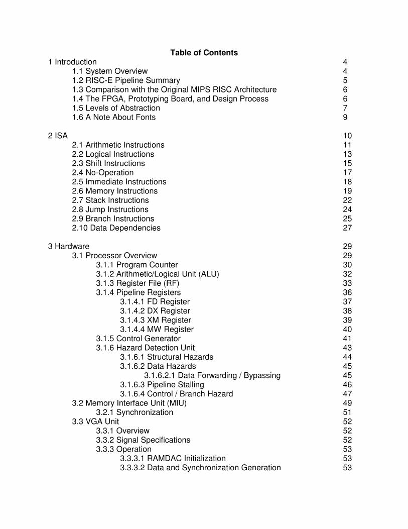
Table of Contents 1 Introduction 4 1.1 System Overview 4 1.2 RISC-E Pipeline Summary 5 1.3 Comparison with the Original MIPS RISC Architecture 6 1.4 The FPGA, Prototyping Board, and Design Process 6 1.5 Levels of Abstraction 7 1.6 A Note About Fonts 9 2 ISA 10 2.1 Arithmetic Instructions 11 2.2 Logical Instructions 13 2.3 Shift Instructions 15 2.4 No-Operation 17 2.5 Immediate Instructions 18 2.6 Memory Instructions 19 2.7 Stack Instructions 22 2.8 Jump Instructions 24 2.9 Branch Instructions 25 2.10 Data Dependencies 27 3 Hardware 29 3.1 Processor Overview 29 3.1.1 Program Counter 30 3.1.2 Arithmetic/Logical Unit (ALU) 32 3.1.3 Register File (RF) 33 3.1.4 Pipeline Registers 36 3.1.4.1 FD Register 37 3.1.4.2 DX Register 38 3.1.4.3 XM Register 39 3.1.4.4 MW Register 40 3.1.5 Control Generator 41 3.1.6 Hazard Detection Unit 43 3.1.6.1 Structural Hazards 44 3.1.6.2 Data Hazards 45 3.1.6.2.1 Data Forwarding / Bypassing 45 3.1.6.3 Pipeline Stalling 46 3.1.6.4 Control / Branch Hazard 47 3.2 Memory Interface Unit (MIU) 49 3.2.1 Synchronization 51 3.3 VGA Unit 52 3.3.1 Overview 52 3.3.2 Signal Specifications 52 3.3.3 Operation 53 3.3.3.1 RAMDAC Initialization 53 3.3.3.2 Data and Synchronization Generation 53

3.3.3.3 Pixel Manipulation 54 3.3.3.4 Character Generation 55 3.3.3.4.1 Decoder Lookup ROM 56 3.4 Keyboard Controller 57 3.4.1 Keyboard-to-Controller Communication 58 3.4.2 Controller-to-Keyboard Communication 59 3.4.3 Structure of the Keyboard Controller 60 3.5 RISC-E Hardware Summary and Execution Trace 63 4 Software 71 4.1 Development Software 71 4.1.1 Sim 71 4.1.1.1 Syntax of Sim 72 4.1.1.2 Programming with Sim 73 4.1.1.3 Instructions in Sim 74 4.1.1.4 Registers and Arguments 75 4.1.1.5 Labels 76 4.1.1.6 Comments and Whitespace 76 4.1.1.7 Reserved word STOP 76 4.1.1.8 I/O (Input / Output) 77 4.1.1.9 bmpgen for Viewing Pixel Output 80 4.1.1.10 Files 82 4.1.2 AssemblerT 83 4.1.3 Assembly Text Generator 90 4.1.4 Bitmap to XES-16 Converter 92 4.2 Board Software 93 4.2.1 Demonstration Programs 93 4.2.1.1 Shell 93 4.2.1.1.1 Interactive Mode 93 4.2.1.1.2 Dispatch Mode 94 4.2.1.2 Etch-a-Sketch 95 4.2.1.3 Fire 96 4.2.1.4 PONG! 96 4.2.1.4.1 Overview 96 4.2.1.4.2 Development 97 4.2.1.5 Snake 98 4.2.2 Test Programs 101 4.2.2.1 AAA 101 4.2.2.2 Alpha 101 4.2.2.3 Echo 102 4.2.3 Stdlib.asm 102 5 Results 103 5.1 Team Member Contributions 104

- 4 -
1 Introduction 1.1 System Overview The RISC-E Microprocessor is a special-purpose MIPS RISC-based system, optimized for character-based (console-style) input/output. RISC-E features a 32-bit five-stage pipelined datapath capable of integer instructions, a complete VGA (Video Graphics Array) interface, and a PS/2 Keyboard Controller. RISC-E also includes some additional instructions designed to streamline assembly-level programming (see 2 ISA). Instruction pipelining and a high-performance ALU ensure short average execution times and high instruction throughput—nonetheless, the programmer will find assembly-level programming in RISC-E to be a straightforward process—with helpful optimizations for I/O and instructions designed to simplify development. Additionally, simulation and assembling tools for the RISC-E architecture speed the testing and debugging process, and a helpful library of function calls reduces repetitive coding. An on-board Memory Interface Unit (MIU) allows the 32-bit RISC-E Microprocessor to operate on a 16-bit development board without any visible changes to processor layout or instruction execution. The core of the RISC-E processor is a 32-bit machine—no design modifications were required to implement the design on the prototyping hardware. As a result, the RISC-E Microprocessor is capable of addressing 218 unique addresses in memory—each of which has width 32 bits—while the underlying hardware has width 16 bits. The peripheral devices have also been designed specifically to simplify character I/O. The PS/2 Keyboard controller interfaces directly with the RISC-E Microprocessor through a dedicated register—nearly invisible to system operation, and easy to access. The controller translates keyboard scan codes to ASCII characters in hardware, greatly simplifying keyboard input. Similarly the VGA Unit accepts ASCII input and prints the corresponding character to the screen without requiring individual pixel manipulation by the processor to produce characters. The result is a very efficient method to perform character-based I/O—without unnecessary software overhead. The register file of the RISC-E Microprocessor includes 32 registers, 28 of which are general-purpose. Any of these registers may be used in a given instruction—there are no restrictions on when a particular register in the file may be addressed. Special purpose registers include a zero register (R0 always fixed at zero), a dedicated I/O register (R29), a stack pointer (R30), and a return-address register (R31). The ALU (Arithmetic/Logical Unit) supports the most common integer operations—add, subtract, shift, rotate, and multiply in a single cycle, allowing for efficient computation and high throughput. Data forwarding and pipeline hazard detection allows the ALU’s utilization to approach 100%. RISC-E’s load/store memory architecture is straightforward, but versatile, allowing the programmer to read or write to any addressable memory location by providing a base

- 5 -
address, an offset and a destination register (for a load word instruction, lw) or a data source register (for a store word instruction, sw). Additionally, push/pop instructions and a self-incrementing/decrementing stack pointer greatly improve the programmer’s ability to employ functions and procedures, even recursion, while maintaining a system stack pointer without mistake-prone arithmetic operations. It is important to note that RISC-E does not include instruction or data caches. In fact, this is not a disadvantage—the memory system is capable of operating at the same speed as the microprocessor itself (in truth, memory operates twice as fast as the processor), and therefore instruction and data caches would provide no added speed benefit. 1.2 RISC-E Pipeline Summary As mentioned above, the RISC-E pipeline has five distinct stages. Stage Abbreviations Purpose Fetch FE, F During the Fetch stage, a given instruction is read
from memory. At the end of Fetch, the instruction is stored in the instruction register.
Decode DE, D During the Decode stage, required values are read from the register file and control signals are generated for a given instruction.
Execute EX, X During the Execute stage, ALU operations are performed and new values of PC are computed. Jumps and branches are evaluated at the end of this stage.
Memory MEM, M During the Memory stage, memory-accessing instructions cause data memory to be accessed. This always causes a Fetch stage to be stalled due to the architectural constraints of RISC-E. If the current instruction does not require access to memory, this stage has no function.
Write-Back WB, W During the Write-Back stage, results of an operation are written to the register file.
Throughout this document, diagrams of instructions in various pipeline stages will be depicted using FDXMW diagrams, similar to the one below. On FDXMW diagrams, execution time is represented on the horizontal axis, and instructions are represented on the vertical axis. Blue arrows denote data-forwarding, red slashes denote pipeline flushes, and the “S” symbol in place of F, D, X, M, or W denotes a pipeline stall.

- 6 -
In the diagram above, forwarding occurs from instruction2’s Execute stage to instruction3’s Execute stage. Additionally, instruction4’s Fetch stage is stalled one cycle, and instruction5 and instruction6 are flushed from the pipe. 1.3 Comparison with the Original MIPS RISC Architecture RISC-E has many similarities with the traditional MIPS RISC architecture:
• 32 registers • 32-bit word length • Similar instruction set, including add, subtract, multiply, logical operations, shift,
conditional branches, jump, load immediate • Load/store memory interface • R30 stack pointer
But RISC-E also includes the following: • Increment and decrement operations, useful in looping • Support for stack-based operations (push/pop) • A built-in PS/2 Keyboard Controller and VGA Controller • Instruction-level support for character I/O, as well as direct pixel manipulation
RISC-E does not afford all of the features of MIPS RISC. It does not support interrupts, floating-point arithmetic, and RISC-E has only one execution mode. However, no aspect of the RISC-E architecture forbids these improvements—for simplicity they were simply omitted. 1.4 The FPGA, Prototyping Board, and Design Process A Xilinx Virtex FPGA (part XSV800HQ240) and development board was used to implement RISC-E in actual hardware. The FPGA has a maximum capability of 800,000 gates—more than sufficient to implement the whole of the RISC-E system. However, board timing constraints limit the performance of RISC-E. The memory layout on the board is organized into two banks—the “left bank” and the “right bank.” It is a design constraint that the only modules permitted to connect directly to the SRAM banks are “Interface” modules, provided in the file mdlring.v. Note that this is not the same module as the Memory Interface Unit, which is a student-designed module. Additionally, the “right bank” is connected directly to the VGA RAMDAC (a required device for VGA output)—and is therefore usable only for displaying pixels. The

- 7 -
right bank is controlled directly by the VGA Unit. The remaining left bank is controlled by the Memory Interface Unit, and comprises the processor’s instruction, data, and stack memory. The RISC-E system was implemented in Verilog HDL, according to the IEEE standard 1364. The design tools provided by Xilinx Inc. and Model Inc. were then used to perform simulation and synthesis of the Verilog code to eventually produce a functional system. Design tools used in this project include:
• HDL Editor Tool used to edit Verilog and VHDL files
• Core Generator System Software tool used to generate often-used logical blocks
• FPGA Express Performs synthesis of Verilog for eventual FPGA implementation
• Design Manager Generates the FPGA-downloadable .bit file which contains the physical layout of the design
• Modelsim An HDL-simulation tool used to observe system operation and diagnose/resolve problems
1.5 Levels of Abstraction The RISC-E system will be presented from several different layers of abstraction. The highest of these, the “top-level,” is defined by the contents of the top-level Verilog module, mdlring. It is laid out as follows:

- 8 -
The top-level modules include two Interface modules (required to interface with the board’s SRAM banks), the MIU module (which handles the processor’s memory accesses), and the processor itself, denoted as the “RISC-E” module above. The next level of abstraction is the “system-level.” It is a view inside the “RISC-E” box pictured above:

- 9 -
The system-level view shows sub-components of the RISC-E Microprocessor. Their purposes and function are explained in detail in 3 Hardware. Note that from the system-level view, the peripherals (VGA Unit and Keyboard Controller) and the MIU are shown as “black boxes,” and that the Interface modules do not appear at all. The peripherals themselves will also be shown at a lower level, each in their individual sections. 1.6 A Note About Fonts Throughout this section of the document, fonts will be used to illustrate key points and commands. Courier font will be used for all program/instruction names and command-line directives.

- 10 -
2 ISA The RISC-E architecture is based on a RISC-type MIPS instruction set, with some extended instructions to aid in the use of the peripherals attached to the processor. The RISC-E architecture includes 28 general purpose registers (registers R1-R28). Register R30 is used as a stack pointer, but if no stack operations are performed, it too could be considered a general purpose register. Register R31 is used by jal (jump and link) instructions to store return IP values, and is by convention used for jr (jump register or jump return) instructions, though it, too, is available for general purpose use. Use of register R29 is limited to the following special purposes:
1) Writes to R29 will write characters (ASCII, lower eight bits only) to the VGA controller as character output, if there is sufficient space in the VGA pixel buffer. Use of the brvid instruction allows a programmer to poll availability of this buffer.
2) Reads from R29 will read characters from the keyboard input controller, if a new key has been depressed. If no key has been depressed, an unspecified value will be read from register R29 (see brchar instruction).
The following registers represent the primary operands for the instruction set following: Key ddddd – 5 bit destination register aaaaa – 5 bit source register A bbbbb – 5 bit source register B ooooo – variable length offset (dependent on instruction type) AAAAA – 18 bit address xxxxx – don’t care field

- 11 -
2.1 Arithmetic instructions Arithmetic instructions perform basic mathematic operations on registered operands and store the result into a register. Opcodes for arithmetic instructions begin with 0h. add
Opcode 31 : 28
Mode 27 : 24
Destination 23 : 19
SrcA 18 : 14
SrcB 13 : 9
8 : 0
0000 0000 ddddd aaaaa bbbbb xxxxxxxxx ddddd � aaaaa + bbbbb add $d $a $b Adds the values in $a and $b together and stores in $d. Works on two’s compliment values and does not consider overflow. sub
Opcode 31 : 28
Mode 27 : 24
Destination 23 : 19
SrcA 18 : 14
SrcB 13 : 9
8 : 0
0000 0001 ddddd aaaaa bbbbb xxxxxxxxx ddddd ��aaaaa - bbbbb sub $d $a $b Subtracts the value in $b from the value in $a and stores the result in register $d. Works on two’s compliment values and does not consider overflow.
Data flow for add and sub instructions.

- 12 -
inc Opcode 31 : 28
Mode 27 : 24
Destination 23 : 19
SrcA 18 : 14
SrcB 13 : 9
8 : 0
0000 0010 ddddd ddddd xxxxx xxxxxxxxx ddddd � ddddd + 1 inc $d Increments the value in register $d by one and stores the result in register $d. dec
Opcode 31 : 28
Mode 27 : 24
Destination 23 : 19
SrcA 18 : 14
SrcB 13 : 9
8 : 0
0000 0011 ddddd ddddd xxxxx xxxxxxxxx ddddd � ddddd – 1 dec $d Decrements the value in register $d by one and stores the result in $d.
Data flow for inc and dec.

- 13 -
mult Opcode 31 : 28
Mode 27 : 24
Destination 23 : 19
SrcA 18 : 14
SrcB 13 : 9
8 : 0
0011 0000 ddddd aaaaa bbbbb xxxxxxxxx ddddd � aaaaa * bbbbb mult $d $a $b Multiplies the lower 16 bits of registers $a and $b and stores the 32 bit result in register $d. Works on two’s compliment values.
Data flow for mult.
2.2 Logical Instructions Logical instructions perform basic logical operations on register operands and store their results in a destination register. and
Opcode 31 : 28
Mode 27 : 24
Destination 23 : 19
SrcA 18 : 14
SrcB 13 : 9
8 : 0
0001 0000 ddddd aaaaa bbbbb xxxxxxxxx ddddd � aaaaa � bbbbb and $d $a $b Performs a bitwise logical AND operation on registers $a and $b and stores the result to register $d. Stores 1 to a given bit if and only if both corresponding bits in $a and $b are 1, 0 otherwise.

- 14 -
or Opcode 31 : 28
Mode 27 : 24
Destination 23 : 19
SrcA 18 : 14
SrcB 13 : 9
8 : 0
0001 0001 ddddd aaaaa bbbbb xxxxxxxxx ddddd � aaaaa | bbbbb or $d $a $b Performs a bitwise logical or operation on registers $a and $b and stores the result to register $d. Stores 0 to a given bit if and only if both corresponding bits in $a and $b are 0, 1 otherwise. xor
Opcode 31 : 28
Mode 27 : 24
Destination 23 : 19
SrcA 18 : 14
SrcB 13 : 9
8 : 0
0001 0010 ddddd aaaaa bbbbb xxxxxxxxx ddddd � aaaaa ^ bbbbb xor $d $a $b Performs a bitwise logical xor operation on registers $a and $b and stores the result to register $d. Stores 1 to a given bit if and only if both corresponding bits in $a and $b are different, 0 if they are the same.
Data flow for and, or, and xor.

- 15 -
not Opcode 31 : 28
Mode 27 : 24
Destination 23 : 19
SrcA 18 : 14
SrcB 13 : 9
8 : 0
0001 0011 ddddd aaaaa xxxxx xxxxxxxxx ddddd � ~aaaaa not $d $a Performs a bitwise logical not operation on register $a and stores the result to register $d. Stores a 1 if the corresponding bit in $a is a 0, and a 0 if the corresponding bit is a 1.
Figure : Picture of data flow for not.
2.3 Shift Instructions Shift instructions move the source register by a value specified in the second source register. sra
Opcode 31 : 28
Mode 27 : 24
Destination 23 : 19
SrcA 18 : 14
SrcB 13 : 9
8 : 0
0010 0000 ddddd aaaaa bbbbb xxxxxxxxx ddddd � { (a[31])^(B%32) , a[31:(B%32)] } sra $d $a $b Shifts register $a to the right by the value in the lower 5 bits of register $b and stores the result in register $d. sra sign extends the value of $a.

- 16 -
srl Opcode 31 : 28
Mode 27 : 24
Destination 23 : 19
SrcA 18 : 14
SrcB 13 : 9
8 : 0
0010 0001 ddddd aaaaa bbbbb xxxxxxxxx ddddd � { 0^(B%32) , a[31:(B%32)] } srl $d $a $b Shifts register $a to the right by the value in the lower 5 bits of register $b and stores the result in register $d. srl does not sign extend the value of $a. sl
Opcode 31 : 28
Mode 27 : 24
Destination 23 : 19
SrcA 18 : 14
SrcB 13 : 9
8 : 0
0010 0010 ddddd aaaaa bbbbb xxxxxxxxx ddddd � { a[31-(B%32):0], 0^(B%32) } sl $d $a $b Shifts register $a to the left by the value in the lower 5 bits of register $b and stores the result in register $d. rol
Opcode 31 : 28
Mode 27 : 24
Destination 23 : 19
SrcA 18 : 14
SrcB 13 : 9
8 : 0
0010 0011 ddddd aaaaa bbbbb xxxxxxxxx ddddd � { a[(B%32)+1,0] , a[31:(B%32)] } rol $d $a $b Shifts register $a to the left by the value in the lower five bits of register $b and fills the lower bits of register $a with the bits of register $a that were shifted out and stores the result in register $d.

- 17 -
ror Opcode 31 : 28
Mode 27 : 24
Destination 23 : 19
SrcA 18 : 14
SrcB 13 : 9
8 : 0
0010 0100 ddddd aaaaa bbbbb xxxxxxxxx ddddd � { a[31:(B%32)], a[(B%32)+1,0] } ror $d $a $b Shifts register $a to the right by the value in the lower five bits of register $b and fills the upper bits of register $a with the bits of register $a that were shifted out and stores the result in register $d.
Data flow for sra, srl, sl, rol, and ror.
2.4 No-Operation No operation performs the addition of register $0 to register $0 and stores the result in register $0. nop
Opcode 31 : 28
Mode 27 : 24
Destination 23 : 19
SrcA 18 : 14
SrcB 13 : 9
8 : 0
0100 0000 00000 00000 00000 xxxxxxxxx nop No operation performs the addition of register $0 to register $0 and stores the result in register $0.
- 18 -
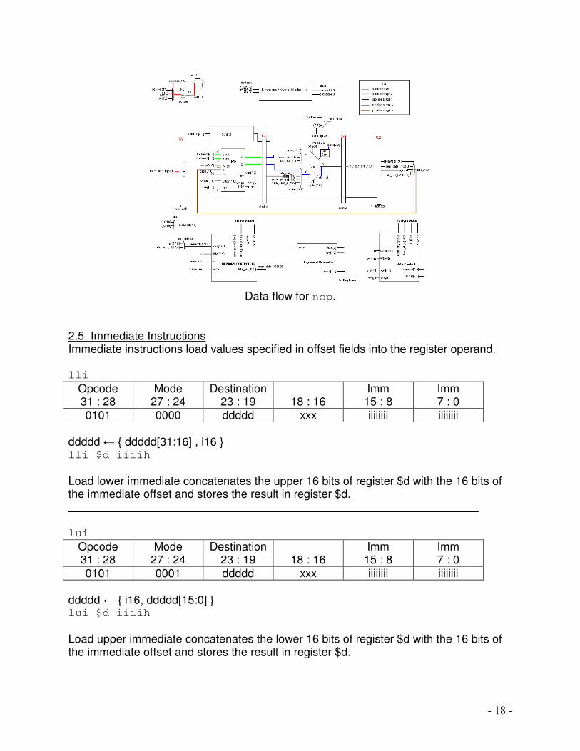
Data flow for nop.
2.5 Immediate Instructions Immediate instructions load values specified in offset fields into the register operand. lli
Opcode 31 : 28
Mode 27 : 24
Destination 23 : 19
18 : 16
Imm 15 : 8
Imm 7 : 0
0101 0000 ddddd xxx iiiiiiii iiiiiiii ddddd � { ddddd[31:16] , i16 } lli $d iiiih Load lower immediate concatenates the upper 16 bits of register $d with the 16 bits of the immediate offset and stores the result in register $d. lui
Opcode 31 : 28
Mode 27 : 24
Destination 23 : 19
18 : 16
Imm 15 : 8
Imm 7 : 0
0101 0001 ddddd xxx iiiiiiii iiiiiiii ddddd � { i16, ddddd[15:0] } lui $d iiiih Load upper immediate concatenates the lower 16 bits of register $d with the 16 bits of the immediate offset and stores the result in register $d.

- 19 -
Data flow for lli and lui.
2.6 Memory Instructions Memory instructions manipulate memory locations by writing to or reading from them. lw
Opcode 31 : 28
Mode 27 : 24
Destination 23 : 19
SrcA 18 : 14
13 : 9
Offset 8 : 0
1000 0000 ddddd aaaaa xxxxx ooooooooo ddddd � MEM[aaaaa + ooooooooo] lw $d $a o Load word reads the memory location specified by the value of register $a plus the offset and stores the result in register $d. Load word creates a unique hazard in the processor, as the MIU runs only fast enough to perform one memory access per clock cycle. Therefore, when a load word is encountered, the pipeline stalls for a cycle to perform the memory read.

- 20 -
Data flow for lw.
sw Opcode 31 : 28
Mode 27 : 24
23 : 19
SrcA 18 : 14
SrcB 13 : 9
Offset 8 : 0
1001 0000 xxxxx aaaaa bbbbb ooooooooo MEM[aaaaa + ooooooooo] � bbbbb sw $b $a o Store words places the value of register $b in the memory location specified by the value of register $a plus the offset. Store word also creates a hazard in the processor, similar to that of load word. When a store word is encountered, the pipeline stalls for a cycle to perform the memory write.

- 21 -
Data flow for sw.
svga Opcode 31 : 28
Mode 27 : 24
23 : 19
18 : 14
SrcB 13 : 9
8 : 0
1001 0001 xxxxx xxxxx bbbbb xxxxxxxxx VGAMEMBUFFNEXT � b svga $b The Store to VGA instruction loads the value in register $b into the VGA buffer queue assuming that the buffer isn’t full (see brpix instruction). The lower 8 bits of register $b are the color, 3 red bits, 2 green bits, and 3 blue bits. The next 20 bits are used to specify the location of the bit to be manipulated (See VGA Unit).

- 22 -
Data flow for svga.
2.7 Stack Instructions Stack instructions load and store values into the address specified by register $30 and increment or decrement register $30 as needed. push
Opcode 31 : 28
Mode 27 : 24
Destination 23 : 19
SrcA 18 : 14
SrcB 13 : 9
8 : 0
1010 0000 xxxxx 11110 bbbbb xxxxxxxxx STACK � b, $30 � $30 – 1 push $b Push stores the value in register $b to the location in memory specified by register $30. Then register $30 is decremented to move the stack pointer.

- 23 -
Data flow for push.
pop
Opcode 31 : 28
Mode 27 : 24
Destination 23 : 19
SrcA 18 : 14
13 : 9
8 : 0
1011 0000 ddddd 11110 xxxxxx xxxxxxxxx $d � STACK pop $d Pop loads register $d with the value at the address specified by register $30. Then register $30 is incremented.
Data flow for pop.

- 24 -
2.8 Jump Instructions Jump instructions change the flow of execution by loading the PC (program counter) with a new value specified by a register or an immediate value. jr
Opcode 31 : 28
Mode 27 : 24
23 : 19
SrcA 18 : 14
13 : 9
8 : 0
0111 0000 xxxxx aaaaa xxxxx xxxxxxxxx PC � aaaaa jr $a Jump register stores the value in register $a into the PC and begins a new program flow. Jumps must flush the pipeline of any instructions that have begun execution erroneously.
Data flow for jr.
jal
Opcode 31 : 28
Mode 27 : 24
Destination 23 : 19
Addr 18 : 14
Addr 13 : 9
Addr 8 : 0
0111 0001 11111 xAAAA AAAAA AAAAAAAAA PC � AAAAAAAAAAAAAAAAAA jal AAAAAh Jump and link loads the PC with the value specified by the offset A. A can be specified as a label or as a numerical offset. Jumps must flush the pipeline of any instructions that have begun execution erroneously.

- 25 -
Data flow for jal.
2.9 Branch Intsructions Branch instructions change the exectuion flow by loading the PC with the current value of the PC plus the offset field. brgt
Opcode 31 : 28
Mode 27 : 24
Offset 23 : 19
SrcA 18 : 14
SrcB 13 : 9
Offset 8 : 0
0110 0001 ooooo aaaaa bbbbb ooooooooo PC � PC + 1 + o brgt $a $b o Branch greater than sets the PC to the value of the PC plus the offset if register $a is greater than register $b. brlt
Opcode 31 : 28
Mode 27 : 24
Offset 23 : 19
SrcA 18 : 14
SrcB 13 : 9
Offset 8 : 0
0110 0010 ooooo aaaaa bbbbb ooooooooo PC � PC + 1 + o brlt $a $b o Branch less than sets the PC to the value of the PC plus the offset if register $a is less than register $b.

- 26 -
breq
Opcode 31 : 28
Mode 27 : 24
Offset 23 : 19
SrcA 18 : 14
SrcB 13 : 9
Offset 8 : 0
0110 0101 ooooo aaaaa bbbbb ooooooooo PC � PC + 1 + o breq $a $b o Branch equal sets the PC to the value of the PC plus the offset if register $a is equal to register $b. br
Opcode 31 : 28
Mode 27 : 24
Offset 23 : 19
18 : 14
13 : 9
Offset 8 : 0
0110 0000 ooooo xxxxx xxxxx ooooooooo PC � PC + 1 + o br o Branch sets the PC to the value of the PC plus the offset unconditionally. brchar
Opcode 31 : 28
Mode 27 : 24
Offset 23 : 19
18 : 14
13 : 9
Offset 8 : 0
0110 0011 ooooo xxxxx xxxxx ooooooooo PC � PC + 1 + o brchar o Branch character sets the PC to the value of the PC plus the offset if a character is ready to be read from the keyboard. brvid
Opcode 31 : 28
Mode 27 : 24
Offset 23 : 19
18 : 14
13 : 9
Offset 8 : 0
0110 0100 ooooo xxxxx xxxxx ooooooooo PC � PC + 1 + o brvid o Branch video sets the PC to the value of the PC plus the offset if the VGA character buffer is ready to be written to.

- 27 -
brpix Opcode 31 : 28
Mode 27 : 24
Offset 23 : 19
18 : 14
13 : 9
Offset 8 : 0
0110 0110 ooooo xxxxx xxxxx ooooooooo PC � PC + 1 + o brpix o Branch pixel sets the PC to the value of the PC plus the offset if the VGA pixel buffer is ready to be written to.
Data flow for branches.
2.10 Data Dependencies There are several forms of data dependencies that occur in this ISA. For instance
add $1 $3 $5 add $1 $1 $5
would create a data dependency because the first add instruction would not write to the register file before the second instruction needed the value in register $1. In order to solve this problem, there is a data forwarding line from the MEM stage to the EX stage which provides the ALU with the value before its written to the register file:
- 28 -
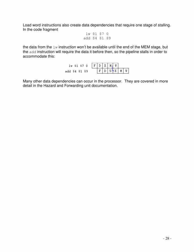
Load word instructions also create data dependencies that require one stage of stalling. In the code fragment
lw $1 $7 0 add $4 $1 $9
the data from the lw instruction won’t be available until the end of the MEM stage, but the add instruction will require the data it before then, so the pipeline stalls in order to accommodate this:
Many other data dependencies can occur in the processor. They are covered in more detail in the Hazard and Forwarding unit documentation.

- 29 -
3 Hardware 3.1 Processor Overview The RISC-E Microprocessor is a 32-bit, five-stage pipelined datapath with accompanying control modules. The five stages of the pipeline in RISC-E are re-summarized below: Stage Abbreviations Purpose Fetch FE, F During the Fetch stage, a given instruction is read
from memory. At the end of Fetch, the instruction is stored in the instruction register.
Decode DE, D During the Decode stage, required values are read from the register file and control signals are generated for a given instruction.
Execute EX, X During the Execute stage, ALU operations are performed and new values of PC are computed. Jumps and branches are evaluated at the end of this stage.
Memory MEM, M During the Memory stage, memory-accessing instructions cause data memory to be accessed. This always causes a Fetch stage to be stalled due to the architectural constraints of RISC-E. If the current instruction does not require access to memory, this stage has no function.
Write-Back WB, W During the Write-Back stage, results of an operation are written to the register file.
The processor’s main components are:
• Program Counter (PC) and Accompanying Logic • Arithmetic Logic Unit (ALU) • Register File (RF) • Pipelining Registers • Control Signal Generator • Hazard Detection Unit
Each of these components will be discussed in subsequent sections of this document.
- 30 -
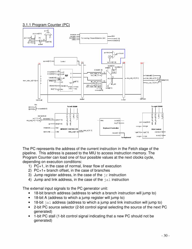
3.1.1 Program Counter (PC)
The PC represents the address of the current instruction in the Fetch stage of the pipeline. This address is passed to the MIU to access instruction memory. The Program Counter can load one of four possible values at the next clocks cycle, depending on execution conditions:
1) PC+1, in the case of normal, linear flow of execution 2) PC+1+ branch offset, in the case of branches 3) Jump register address, in the case of the jr instruction 4) Jump and link address, in the case of the jal instruction
The external input signals to the PC generator unit:
• 18-bit branch address (address to which a branch instruction will jump to) • 18-bit A (address to which a jump register will jump to) • 18-bit jal address (address to which a jump and link instruction will jump to) • 2-bit PC source selector (2-bit control signal selecting the source of the next PC
generated) • 1-bit PC stall (1-bit control signal indicating that a new PC should not be
generated)

- 31 -
• 1-bit branch taken (1-bit flag indicating if a branch is taken) • 1-bit mode[0] (the least significant bit of mode, which is the 24th bit of an
instruction). The external output signals of the PC generator unit:
• 18-bit PC (18-bit memory address, which is used in memory access at the next clock cycle)
• 18-bit incremented PC (18-bit PC+1, which is used in PC generation calculation at the next clock cycle).
The illustration below depicts all operating modes of the PC module:
The reset behavior of the Program Counter determines the first instruction fetched and executed by the RISC-E Microprocessor. This first address is 00000h.

- 32 -
3.1.2 Arithmetic/Logic Unit (ALU)
The ALU performs the arithmetic operations (add, subtract, increment, decrement, and multiply) and logical operations (shift, rotate, AND, and OR). The type of operation is determined by the 4-bit mode signal and the 3-bit execution control signal. The external input to the ALU:
• 32-bit A and B (two 32-bit operands) • 4-bit mode (the second most significant 4-bits of an instruction) • 3-bit execution control (3-bit control signals sent by the control generator) • 3-bit I/O status (flag indicating keyboard input availability or VGA pixel/character
buffer readiness). The external output signals of the ALU:
• 32-bit O (32-bit results of an ALU operation) • 1-bit branch taken (flag indicating that conditional branch should be taken based
on the result of an ALU operation).

- 33 -
ALU Operations Table exctrl mode Operation 0h 0h add operands 1h subtract operands 2h increment operand A 3h decrement operand A 1h 0h AND operands 1h OR operands 2h XOR operands 3h NOT operand A 2h 0h Shift Operand A Left by (Operand B % 32) 1h Shift Operand A Right with Sign Extension by (Operand B % 32) 2h Shift Operand A Right without Sign Extension by (Operand B % 32) 3h Rotate Operand A Left by (Operand B % 32) 4h Rotate Operand A Right by (Operand B % 32) 3h 0h Concatenate upper 16-bits of Operand A with lower 16-bits of Operand
B to form {A[31:16],B[15:0]} 1h Concatenate lower 16-bits of Operand B with lower 16-bits of Operand
A to form {B[15:0], A[15:0]} 4h n/a multiply lower 16-bits of operands to produce 32-bit result 5h 0h If operands equal, assert signal brtaken 1h If Operand A > Operand B, assert signal brtaken 2h If Operand A < Operand B, assert signal brtaken 3h If Keyboard Input Available, assert signal brtaken 4h If VGA Character Buffer not full, assert signal brtaken 5h If VGA Pixel Buffer not full, assert signal brtaken 6h n/a add operands (computes memory address) 7h n/a add operands (computes top-of-stack address) The ALU performing some of the above functions:

- 34 -
3.1.3 Register File (RF)
The Register File (RF) is a collection of registers (in this architecture, 32 registers) in which any register can be read or written by specifying the number of the register in the file. Like the MIPS RISC architecture, most registers in the RISC-E architecture are built for general purposes, except:
• Register R0 – Always zero-valued • Register R29 – reserved for I/O-related operations • Register R30 – reserved for stack pointer • Register R31 – serves as a general-purpose register as well as storage for return
address of jal operation Register R29 is used in a streamlined character I/O:
• After a key on the keyboard is pressed, the character can be read from register R29
• To print a character to the VGA screen, the character should be written to register R29
Register R30 is used in stack-based operations: • In response to a push instruction, register R30 will decrement itself

- 35 -
• In response to a pop operation, register R30 will increment itself The external input signals to the RF:
• 5-bit addresses of A and B (registers that will be a possible source for ALU operands)
• 5-bit address of destination register (register where data will be written in a given clock cycle)
• 32-bit data (32-bit data to be written to a destination register in the RF) • 1-bit RF write (1-bit control signal indicating a write to the RF to be performed) • 2-bit register R30 control (2-bit control signal indicating the type of operation to
be performed on register R30, if any) • 8-bit keyboard input (8-bit character sent by the keyboard controller)
The external output signals of the RF:
• 32-bit value of register A and B • 1-bit wvga, which pulses high in response to a write to R29, signaling the VGA
Unit to write a new character to the screen • 1-bit rkey, which pulses high in response to a read from R29, acknowledging to
the Keyboard Controller that a key has been read • 8-bit vga, containing the last value written to register R29.

- 36 -
The Register File in the RISC-E architecture is implemented using two Dual-Port Block Memory (DPBM) components generated by the Core Generator Software, as is indicated by the partial schematic above. Using two DPBM components allows two reads and one write to occur in a single clock cycle without need for additional clocking signals. Additionally, special-purpose registers R0, R29, and R30 are implemented using flip-flops, and are multiplexed into the data outputs as necessary (addresses 0, 29, and 30 are unused in the DPBMs). Implementing these registers using the FPGA’s flip-flops enabled their special functions—that is, R30 can self increment/decrement, and R29 is always visible to the VGA Unit. Note that values written to R29 cannot then be read from R29. R29 always “reads” the last value sent by the keyboard, regardless of writes to this register. Values written to this register are passed to the VGA unit, and are not readable once they have been written. The Register File also plays a key role in the data forwarding schemes of the RISC-E architecture. Should a write address equal a read address at any given time, the incoming data is automatically forwarded to the appropriate read port of the register file, without need of external signals. Therefore, there is never any need to perform data forwarding from the Write-Back stage of the pipeline to the Decode stage.
3.1.4 Pipeline Registers Pipeline registers physically separate pipeline stages in the processor, and propagate signals and/or data from one stage of the pipe to the next. There are four pipeline registers in the RISC-E processor.
1) FD register: between fetch (FE) and decode (DE) stage 2) DX register: between decode (DE) and execute (EX) stage 3) XM register: between execute (EX) and memory (MEM) stage 4) MW register: between memory (MEM) and write-back (WV) stage
Pipeline registers have the following capabilities not found in a typical register:
1) Able to stall (re-load their current value on next clock) in response to input stall signal high at a clock edge
2) Able to flush (synchronously clear) in response to input flush high at clock edge Note: Signal flush overrides signal stall.

- 37 -
3.1.4.1 FD Register
The FD register controls propagation of signals from the Fetch stage to the Decode stage of the pipeline. The input signals to the FD register:
• 1-bit stall (1-bit control signal indicating if FD register needs to be stalled) • 1-bit flush (1-bit control signal indicating if FD register should be flushed) • 18-bits PC+1 at ‘t’ (18-bit incremented PC). • 32-bits Instr—the instruction read from memory during a Fetch cycle
The output signals of the FD register:
• 18-bits PC+1 at ‘t+1’ (18-bit incremented PC after 1 clock cycle). • 32-bits Instr at ‘t+1’ (instruction to be decoded during the Decode stage)

- 38 -
3.1.4.2 DX Register
The DX register controls propagation of signals from the Decode stage to the Execute stage of the pipeline. The input signals to the DX register:
• 1-bit stall (1-bit control signal indicating if DX register needs to be stalled) • 1-bit flush (1-bit control signal indicating if DX register should be flushed) • 4-bit opcode at ‘t’ (4 most significant bits of an instruction) • 32-bit register A and B at ‘t’ (2 32-bit value of register A and B generated by the
register file) • 16-bit control bus (16-bit control bus to be propagated for later operations,
including: register 30 control, RF write, RF data selector, memory write, memory read, PC source selector, source B selector, execution control, and memory address selector)
• 28-bit instruction at ‘t’ • 18-bit PC+1 at ‘t+1’.
The output signals of the DX register:

- 39 -
• 4-bit opcode at ‘t+1’ • 28-bit instruction at ‘t+1’ • 32-bit register A and B at ‘t+1’ • 16-bit control bus at ‘t+1’ • 18-bit PC+1 at ‘t+2’.
3.1.4.3 XM Register
The XM register controls propagation of signals from the Execute stage to the Memory stage of the pipeline. The input signals to the XM register:
• 1-bit stall (1-bit control signal indicating if XM register needs to be stalled) • 1-bit flush (1-bit control signal indicating if XM register should take into account
the input signals) • 32-bit value of register B (32-bit contents of register B, coming out from the RF) • 32-bit value of ALU result at ‘t’

- 40 -
• 8-bit control bus at ‘t+1’ (8-bit control bus, which is part of control bus at ‘t’, including: register 30 control, RF write, RF data selector, memory write, memory read, and memory address selector)
• 5-bit address of destination register • 5-bit addresses of source operands (total of 10 bits) • 4-bit opcode at ‘t+1’
The output signals of the XM register:
• 32-bit value of register B • 32-bit value of ALU result at ‘t+1’ • 8-bit control bus at ‘t+2’ • 5-bit address of destination register • 5-bit addresses of source operands (total of 10 bits) • 4-bit opcode at ‘t+2’
3.1.4.4 MW register
The MW register controls propagation of signals from the Memory stage to the Write-Back stage of the pipeline.

- 41 -
The input signals to the MW register: • 1-bit stall (1-bit control signal indicating if MW register needs to be stalled) • 1-bit flush (1-bit control signal indicating if MW register should take into account
the input signals) • 32-bit value of ALU result at ‘t+1’ • 7-bit control bus at ‘t+2’ • 5-bit address of destination register
The output signals of the MW register:
• 32-bit value of ALU result at ‘t+2’ • 7-bit control bus at ‘t+3’ • 5-bit address of destination register
3.1.5 Control Generator
The Control Generator is responsible for generating all non-hazard, non-forward related control signals for all pipeline stages after Decode (that is, Execute, Memory, and Write-Back). The Control Generator takes as input the current opcode and current mode bits

- 42 -
(eight bits in total) and produces all required control signals for the Execute, Memory, and Write-Back pipeline stages. The external input signals to the control generator unit:
• 4-bit opcode (the most significant 4-bit of an instruction) • 4-bit mode (the next most significant 4-bit of an instruction)
The external output signals of the control generator unit:
• 2-bit PC selector (2-bit control signals selecting the source of PC) • 1-bit read to the memory (1-bit control signal indicating that data is to be read
from memory during the Memory stage) • 1-bit write to the memory (1-bit control signal indicating that data is to be written
to memory during the Memory stage) • 3-bit source B selector (3-bit control signals selecting the source of register B, the
second operand of the ALU during the Execution stage) • 3-bit execution control (3-bit control signals indicating which ALU operation to be
performed during the Execution stage) • 2-bit register file data selector (2-bit control signal selecting the source of data to
be written to the register file during the Write-Back stage) • 1-bit write to the register file (1-bit control signal indicating if data is to be written
to the register file during the Write-Back stage) • 2-bit register 30 control (2-bit control signals indicating the type of operation to be
performed on register 30 – stack pointer) • 1-bit memory address selector (1-bit control signal selecting the source of
memory address) • 1-bit write to the VGA (1-bit control signal indicating if a pixel to be written to the
VGA controller)

- 43 -
3.1.6 Hazard Detection Unit
The Hazard Detection Unit is responsible for detecting the following events and acting accordingly:
1) Structural hazard 2) Data hazard 3) Control / Branch hazard
The external input signals to the Hazard detection Unit:
• 5-bit FD register A and B (two 5-bit addresses of register A and B originating from FD register)
• 5-bit DX register A and B (two 5-bit addresses of register A and B originating from DX register)
• 1-bit DX memory read and write (two 1-bit control signal indicating if a read or a write to the memory is to be performed)
• 1-bit XM register file write (1-bit control signal indicating if a write to the RF to be performed)
• 5-bit XM register D (5-bit address of destination address coming from XM register)

- 44 -
• 1-bit XM memory read and write (2 1-bit control signal indicating if a read or a write to the memory to be performed)
• 1-bit MW register file write (1-bit control signal indicating if a write to the RF to be performed)
• 5-bit MW register D (5-bit address of register used as a destination register in WB stage)
• 1-bit MW memory read and write • 1-bit branch taken
The external output signals of the hazard detection unit:
• 2-bit source A forwarding selector (2-bit control signals selecting the source of register A, the first ALU operand)
• 2-bit source B forwarding selector (2-bit control signals selecting the source of register B, the second ALU operand)
• 1-bit PC stall (1-bit control signal indicating if PC needs to be stalled) • 1-bit fetch stall (1-bit control signal indicating if FD register needs to be stalled) • 1-bit fetch flush (1-bit control signal indicating if the output of FD register should
be discarded) • 1-bit decode stall (1-bit control signal indicating if DX register needs to be stalled) • 1-bit decode flush (1-bit control signal indicating if the output of DX register
should be discarded) • 1-bit execution stall (1-bit control signal indicating if XM register needs to be
stalled) • 1-bit execution flush (1-bit control signal indicating if XM register needs to be
flushed) • 1-bit memory flush (1-bit control signal indicating if MW register needs to be
flushed) 3.1.6.1 Structural Hazards Structural Hazards arise due to system resource conflicts. In the RISC-E architecture, there are four cases of structural hazards—all of which are related to accessing data memory:
1) Load word (lw) instruction 2) Store word (sw) instruction 3) Push register to the stack (push instruction) 4) Pop register from the stack (pop instruction)
Each of the four cases above requires a data memory access. In the RISC-E architecture, instruction and data memory share a single I/O port, and as a consequence of pipelining, a subsequent Fetch stage must be stalled. During the cycle that Fetch is stalled, the data memory access (lw, sw, push, or pop in the Memory cycle) can be performed. For more information on pipeline stalls, including examples and waveforms, see section 3.1.6.3 Pipeline Stalling.

- 45 -
3.1.6.2 Data Hazards Data hazards are caused by the dependency of an instruction on the results of previous instruction(s) in the pipeline. There are two solutions to prevent this hazard, depending on the instructions:
1) Data forwarding / bypassing 2) Pipeline stalling
All data hazards in the RISC-E Microprocessor are solved by one of the above means. 3.1.6.2.1 Data Forwarding / Data Bypassing Data forwarding is a solution to prevent a data hazard by routing the missing value to where it is required from a later stage in the pipeline. Data Forwarding is a viable solution for the following Data Hazards:
1) EX hazard One of the ALU operands is needed from the result of previous ALU operation (which is now in the MEM stage): The result of the previous instruction is fed back as an input to the ALU without waiting for the value to be written back to the register file. Consider the following code example:
sub R1 R4 R5 add R7 R1 R9
Note the data dependency of R1. The FDXMW diagram of this dependency:
The forwarding path from the signal aluout_tp1 to ALU source A is activated:

- 46 -
2) MEM hazard One of the ALU operands is needed from data memory or an earlier ALU result (which is now in the WB stage): This value is fed back as an input to the ALU. Consider the following code example: sub R1 R4 R5 lli R8 1234h add R7 R1 R9 A dependency of R1 still exists, now between the WB stage of the sub instruction and the EX stage of the add instruction:
The forwarding path from the WB stage to the ALU is activated:
A capture of the RISC-E Microprocessor as it performs data forwarding:
3.1.6.3 Pipeline Stalling Pipeline stalling is a method to resolve data and structural hazards by preventing some pipeline stages from loading new values. Thereby, an instruction in a given stage is “stalled” while unstalled instructions make forward progress. Pipeline stalls occur for one of two reasons in the RISC-E Microprocessor:

- 47 -
1) A memory-access instruction has entered the MEM stage of the pipe: Since RISC-E affords only one memory port to the MIU, a subsequent Fetch stage must be stalled.
2) A load word (lw) instruction has been executed, and an instruction immediately following requires the value from memory as an operand.
Both of these conditions can be demonstrated with a example. Consider the following code segment:
lw R1 R7 0 add R4 R1 R9
Clearly, a data dependency exists between these two instructions (R1). However, since the load word instruction accesses memory, a Fetch must be stalled. Additionally, the value of R1 will not be available until the lw instruction completes the MEM stage, though its value is required for the add instruction’s EX stage. Hence, a second stall.
A capture of the RISC-E processor stalling for memory instructions:
3.1.6.4 Control Hazard / Branch Hazard Control Hazards occur due to changes in the flow of execution resulting from a branch or jump instruction. These instructions are evaluated upon reaching the EX stage of the pipeline—at that time, PC is updated with its “new” value. It is this sudden (non-increment) change in the instruction pointer that causes a control hazard.

- 48 -
When a jump or branch reaches the EX stage, two other instructions have already entered the pipeline, and are in the Fetch and Decode stages when the PC update is evaluated. These instructions cannot be allowed to complete execution—they must be flushed from the pipe. The pipeline registers are designed for this eventuality. Consider the following code from a test program: br NOCLEAR xor R8 R0 R0 :NOCLEAR breq R8 R0 NOWORK nop The code above is meant to test the pipeline’s ability to detect and remedy Control Hazards. Note that if the xor instruction is not properly flushed (after the br instruction is evaluated) then the breq instruction that follows it will be taken, signaling that the flush failed. However, the breq instruction will not be taken should the xor instruction be correctly flushed from the pipe.
The RISC-E Microprocessor flushing the pipeline after branches are taken:
- 49 -
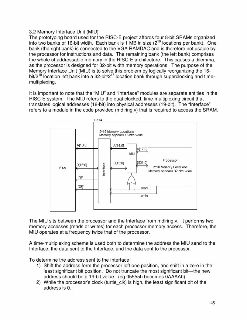
3.2 Memory Interface Unit (MIU) The prototyping board used for the RISC-E project affords four 8-bit SRAMs organized into two banks of 16-bit width. Each bank is 1 MB in size (219 locations per bank). One bank (the right bank) is connected to the VGA RAMDAC and is therefore not usable by the processor for instructions and data. The remaining bank (the left bank) comprises the whole of addressable memory in the RISC-E architecture. This causes a dilemma, as the processor is designed for 32-bit width memory operations. The purpose of the Memory Interface Unit (MIU) is to solve this problem by logically reorganizing the 16-bit/219 location left bank into a 32-bit/218 location bank through superclocking and time-multiplexing. It is important to note that the “MIU” and “Interface” modules are separate entities in the RISC-E system. The MIU refers to the dual-clocked, time-multiplexing circuit that translates logical addresses (18-bit) into physical addresses (19-bit). The “Interface” refers to a module in the code provided (mdlring.v) that is required to access the SRAM.
The MIU sits between the processor and the Interface from mdlring.v. It performs two memory accesses (reads or writes) for each processor memory access. Therefore, the MIU operates at a frequency twice that of the processor. A time-multiplexing scheme is used both to determine the address the MIU send to the Interface, the data sent to the Interface, and the data sent to the processor. To determine the address sent to the Interface:
1) Shift the address form the processor left one position, and shift in a zero in the least significant bit position. Do not truncate the most significant bit—the new address should be a 19-bit value. (eg 05555h becomes 0AAAAh)
2) While the processor’s clock (turtle_clk) is high, the least significant bit of the address is 0.

- 50 -
3) While the processor’s clock (turtle_clk) is low, the least significant bit of the address is 1.
Therefore, if the processor reads from logical addresses 00000h, 00001h, and 1570Ah, the MIU will read from physical addresses 00000h, 00001h, 00002h, 00003h, 2AE14h, and 2AE15h. To determine the data sent to the Interface:
1) When the processor’s clock (turtle_clk) is high, the least significant 16 bits are sent to the Interface, regardless of read/write cycles.
2) When the processor’s clock (turtle_clk) is low, the most significant 16 bits are sent to the Interface, regardless of read/write cycles.
Therefore, the least significant 16 bits of a word are always stored at the lower of the two physical address corresponding to a logical address. To determine the data sent to the processor:
1) At the negative edge of the processor’s clock (turtle_clk), the value from memory is latched into the 16-bit time_mux register.
2) The upper 16 bits of the data bus to the processor is always equal to the value read from memory. The lower 16 bits are assigned to the time_mux register.
Thus, reading from memory is accomplished by time-multiplexing the data bus. It is important to note that by writing a value to a memory location then reading from that memory location will return the value that was written—that is, the least significant and most significant 16 bits will not be swapped. To illustrate:
In the example above, turtle_clk is the processor’s clock, and cheetah_clk runs at twice turtle_clk’s speed. The we (bar) and oe (bar) signals are generated from the Interface unit: oe (bar) low indicates a memory read, we (bar) low indicates a memory write. The “addr” bus corresponds to the address generated by the MIU. The “data” bus represents the actual data as it is read from the RAM. Note that near the end of the capture, the “bar” bus transitions to 3Fh—this indicates that the value read from memory is exactly identical to the value written to memory in the previous clock cycle.

- 51 -
3.2.1 Synchronization A finite state machine controls the MIU’s reset behavior. It is made up of four distinct states—RESET, WAIT_CLOCKS, WAIT_SIGS, and RUN. The state register is clocked on the negative edge of cheetah_clk, and operates as follows:
State RESET: The MIU enters this state in response to both dll_reset (the reset for the system-wide clock buffers) and reset (the normal system reset) being asserted. State WAIT_CLOCKS: After the reset condition ends, the MIU will not leave the WAIT_CLOCKS state until an oscillator driven by turtle_clk changes its value. This state exists to ensure that all relevant system clocks are actually oscillating before attempting to synchronize timing with the processor. Note if this state is reached, cheetah_clk must be running (as the FSM is controlled by cheetah_clk) and therefore only turtle_clk need be tested. Also note that during this state it is assumed that reset is still asserted (eg the processor is still in reset and has yet attempted to access memory). State WAIT_SIGS: The MIU will transition out of this state when the processor makes its first memory access request. This state exists to ensure that memory accesses will begin when turtle_clk is high and an oscillator of turtle_clk is properly initialized. This oscillator is used to drive the least significant bit of the address—should this bit fail to initialize correctly, memory accesses will occur “backwards.” State RUN: The MIU will only leave the RUN state due to a reset. After the sink state RUN is reached, the MIU address will always be correct—it will be even-valued when turtle_clk is high and odd-valued when turtle_clk is low.

- 52 -
3.3 VGA UNIT 3.3.1 Overview The VGA unit is responsible for reading the contents of the right SRAM for the RAMDAC to interpret into colors and for providing the proper synchronization signals to the monitor it is connected to. It also interfaces with the processor to allow character generation and individual pixel manipulation, and initializes the color table of the RAMDAC as well. The VGA provides 368 x 480 resolution in 256 colors and runs off of a 17.5 MHz clock.
VGA Interface Diagram 3.3.2 Signal Specifications
Signal Name Direction Description blankb Output When low it causes the RAMDAC to ignore incoming color
data and provide black to the monitor charin input Character data in ASCII format from the processor
clk input Clock signal for all registers in the unit (17.5 MHz) d output Data for initializing the RAMDAC
hsyncb output Signals the beginning of a new horizontal line and causes the monitor’s electron gun to move back to the left of the screen
pixelin input Pixel data from the processor ra output Address for the right SRAM

- 53 -
rd output Data for the right SRAM rdb output Active low read enable for the RAMDAC initialization that is
always held high roeb output Active low read enable for the right SRAM
rs output Specifies what you are writing to in the RAMDAC rweb output Active low write enable for the right SRAM sw input Active low reset signal for the entire VGA unit
trste output Held high to signal the RAMDAC is in use and not the Ethernet port
vsyncb output Signals the start of a new frame on the monitor and causes the electron gun in the monitor to restart at the top of the screen
wrb output Active low write enable for the RAMDAC initialization wrchar input Active high write enable from the processor to signal a new
character has been written writecharok output Corresponds to the iostat[2] signal within the processor and
signifies that the VGA unit is ready to accept a character write when high
writepixok output corresponds to the iostat[2] signal within the processor and signifies that the VGA unit is ready to accept a pixel write when high
wrpix input Active high write enable from the processor to signal a new pixel has been written
3.3.3 Operation 3.3.3.1 RAMDAC Initialization Upon reset the initialization module of the VGA unit begins to set up the RAMDAC for operation. It begins in the mask state, which writes the RAMDAC mask register to FFh so the RAMDAC does not ignore any color input, the mask register is specified by setting rs to 2. The next state writes the command A register of the RAMDAC to 0 specifying that the color mode will be 256 colors, the command A register is specified by setting rs to 6. After writing the command A register the color table is written to the RAMDAC. It is done by repeatedly writing an 8-bit address to the RAMDAC then writing the red color value, the green color value and finally the blue color value. To write the address rs is set to 0 and to write color values rs is set to 1. The colors in the table are mapped in the following way: red[7:5]=addr[7:5], red[6:0]=0, green[7:6]=addr[4:3], green[5:0]=0, blue[7:5]=addr[2:0], blue[4:0]=0. For example the 8-bit color F0 would map to the 24-bit color E08000. Once all 256 values of the color table have been written the initialization module goes into an idle state and stays there. 3.3.3.2 Data and Synchronization Generation The control module is responsible for making color data appear on the RAMDAC/SRAM bus in the correct order as well as generating the synchronization and blanking signals. To do this the control implements two counters the clock counter and line counter. The clock counter increments every clock cycle and goes to zero once it reaches 549. The line counter increments every time the clock counter reaches 549 and returns to zero

- 54 -
when it reaches 531. Pixel data is read out of the ram whenever the clock counter is lower than 368(the horizontal resolution) and the line counter is lower than 480(the vertical resolution). Whenever the clock counter is 368 or higher or the line counter is greater than or equal to 480 the blanking signal is driven low. When the clock counter is between 418 and 486 the horizontal sync is driven low, and whenever the line counter is between 491 and 494 the vertical sync is driven low. Generating the address of the pixel for the SRAM is done as follows: addr[18]=0, addr[17:9]=line_counter, addr[8:0]=clock_counter. This causes the data from the SRAM to appear on the bus for the RAMDAC as the controller is cycling through the synchronization timing.
VGA Controller Specifications Resolution 368 x 480 Horizontal Sync Rate 31.88 kHz Vertical Sync Rate 60.03 Hz Horizontal Front Porch 2.91 us Horizontal Sync Pulse Width 3.89 us Horizontal Back Porch 3.60 us Vertical Front Porch 0.35 ms Vertical Sync Pulse Width 0.01 ms Vertical Back Porch 1.19 ms
VGA Timing Specifications Waveform 3.3.3.3 Pixel Manipulation The VGA controller module is also responsible for accepting pixel data from the processor and storing it in the right SRAM to be read out to the RAMDAC. It has a FIFO within it to store pixel data until the blanking signal goes low and the pixels can be written out to the right SRAM. The FIFO is synchronous with empty and full signals and is 32 bits wide by 128 tall. The writepixok signal(iostat[2] in the processor) signifies when the controller is ready to accept a pixel from the processor. The processor has the brpix branch dedicated for checking iostat[2] so it can poll for controller readiness. The active high iostat[2] signal is high when the FIFO is not full and when the blanking signal is not active. When a pixel is written the processor sends the wrpix signal high and the controller then writes the pixel to the FIFO. The controller expects the pixel data from the processor to be in the form: pix[7:0]=color, pix[16:8]=x-coordinate, pix[26:18]=y-coordinate. Extra room was left between the coordinates in the pixel data

- 55 -
to allow for higher resolutions that may require more bits to specify the coordinates. During a blanking signal if the FIFO has data in it, it is read out and split into the corresponding fields and then written to the right SRAM so it will be displayed. 3.3.3.4 Character Generation The character decoder module interfaces with both the processor and the controller module. The decoder has the writecharok signal (iostat[1] in the processor) to signal when the controller register is ready for a new character from the processor. It is high whenever the register is empty and the processor can poll for the decoder's readiness with the brvid branch instruction. After determining the decoder is ready, the processor then sends the character to be printed to register R29 and asserts the wrchar signal high which enables the write on the decoder register. The character sent to the decoder is expected to be in ASCII format. Once the decoder has received a character it moves from the idle state to the decode state. In the decode state it is determined whether the character is printable or not. If the character is not printable but modifies the cursor position(see the table below for a description of character functions) of the screen the cursor position is updated. If the character is not printable and does not modify the cursor position it is simply ignored and the decoder goes back to the idle state. For printable characters each individual pixel is looked up in a ROM that is placed on the block select RAM (the ROM is described in detail in the next sub-section). Once the pixel data has been decoded the pixel is sent to the controller through the same interface the processor uses to manipulate pixels. When the decoder is sending data to the controller it de-asserts the writepixok signal so the processor does not attempt to write pixels at the same time the decoder is. After all the pixel data has been sent for a character the cursor position is updated and then the decoder resumes the idle state. When a character is printed the cursor is moved eight pixels right (one character wide), unless it is at the end of a line, in which case it is moved all the way to the left and down 10 pixels (one character high). If the cursor is in the bottom right corner of the display it remains there and all subsequent character writes overwrite that position, until the cursor is modified with a non-printable character.
Non-Printable Character Functions Hex Value Character Function
8 Backspace Moves cursor to the left one position, if the cursor is at the left of the screen already, it moves it to the last spot on the line above
9 Horizontal Tab Moves the cursor 5 characters right and stops at the right side of the screen
10 Newline Moves the cursor down one line without moving it horizontally
11 Vertical Tab Moves the cursor down five lines 12 Form Feed Moves the cursor to the upper right of the screen 13 Carriage
Return Moves cursor all the way to the left without changing vertical position
Note: Enter can be simulated in software by sending both a newline and carriage return.
Backspace(erase) can be simulated in software by sending backspace, space, backspace.

- 56 -
3.3.3.4.1 Decoder Lookup ROM The decoder lookup ROM was generated in three steps. The first step was creating a font definition, to do this a program from the internet called fontgen was used. It takes as parameters the characters to be generated, the font name and font size. It generates a text file that contains images of the character's and hex descriptions of each pixel row of the characters, a 1 meaning that column of the particular row is part of the character and a 0 meaning that column of the row is part of the background. The characters were generated in the same order as the ASCII table to make looking them up a simple process. The following is an example of the output: 0x00, /* [ ] */ 0x78, /* [ **** ] */ 0xCC, /* [** ** ] */ 0x0C, /* [ ** ] */ 0x0C, /* [ ** ] */ 0x38, /* [ *** ] */ 0x0C, /* [ ** ] */ 0x0C, /* [ ** ] */ 0xCC, /* [** ** ] */ 0x78, /* [ **** ] */ 0x00, /* [ ] */
The next step in creating the lookup ROM was to convert the font definition file into a ROM-file to be used by the core generator. We created a program called coemaker that parsed the hex values from the font definition file and placed them in the ROM-file. The hex values were padded out to sixteen bits so that each row of the character would correspond to one address in the ROM. The coemaker also ignored the top row of each character to truncate them all to ten columns high. The final step of creating the ROM was done with the core generator. Using the input file we created a synchronous ROM to be placed in the block select RAM. To get pixel data from a character the decoder has a row and column register. To generate the address for the character row in the ROM the decoder used the following formula: addr = (ascii_value-32)*16 + row Thirty-two is subtracted from the ASCII value to compensate for the offset of the first printable character from the actual beginning of the ASCII table. That value is then multiplied by sixteen because there are sixteen rows allocated to each character in the ROM, and row is added to get the particular row that is currently being looked up. Once the row is obtained the decoder gets the bit corresponding to the current column and if it is one sets the pixel color to the value of the text color register, otherwise it is set to the value of the background color register. The text color and background color of the characters can be modified by the processor with the svga instruction: If bit 31 of the pixels data sent to the VGA unit is 1, the data is not printed to the monitor (because it is off of the displayable screen) and the character decoder loads the text color register with the lowest 8-bits and the background color register with the next lowest 8-bits.

- 57 -
3.4 Keyboard Controller An integral part of the RISC-E character I/O system is the keyboard controller. Its function is to interface with a standard PS/2 keyboard and send user input to the processor. Logically, the processor views the keyboard controller as a peripheral device that can be accessed through the I/O register, R29 (through signals rkey and key[7:0]):
A status line (iostat[0]) is routed to the ALU for evaluation of the brchar branch instruction. This line transitions high when a new character becomes available, and transitions low after the character has been retrieved by the processor. The PS/2 is an open-collector (synchronous) serial interface. Thus, PS/2 is two-valued: Low (approximately 0 V) or High-Impedance (reads as logic high, or 5 V).
Therefore, it is not possible to drive the ps2data or ps2clk signals to a high state. The signals are instead released from the low state, and the pull-up resistors bring the signals to a logic-high, high-impedance state. It is the responsibility of the PS/2 device (eg the keyboard) to generate clock signals. The clock frequency may range between 10kHz and 16.7kHz—the keyboard controller will operate at any ps2clk frequency less than 1 MHz. The only time the controller pulls the clock line low is to request that the device begin generating clocking signals, and thereby initiate communication (see Controller-to-Keyboard Communication, below).

- 58 -
3.4.1 Keyboard-to-Controller Communication A standard PS/2 keyboard will initiate communication with the keyboard for one of the following reasons:
1) The user has depressed a key 2) The user is holding a key 3) The user has released a key 4) The keyboard is acknowledging a communication from the controller that
requires an eight-bit acknowledge. (1-bit acknowledge is present for all controller-to-keyboard communications, see below)
5) A parity error has occurred, the keyboard is requesting a re-send of the last packet.
The keyboard controller implemented in the RISC-E system handles all of the above conditions. When initiating communications, the device (keyboard) pulls the ps2data line low, and sends begins sending clock pulses to the controller. Following (synchronously with respect to ps2clk) are the data bits (big-endian), a parity bit (odd parity) and a stop bit (always binary 1). Therefore, each keyboard-to-controller communication will be 11 bits in length.
Typically, only one 11-bit packet is sent, but conditions may arise such that the keyboard will send up to three 11-bit packets, which must be considered as a single message (message length therefore varies: [1,3]). For instance, the signal corresponding to the right CONTROL key released is: E0h followed by F0h followed by 14h. The content of the data packets usually consists of keyboard scan codes (make/break codes). These codes are not ASCII values—they are themselves a unique representation of all keys on a standard PS/2 keyboard. (for a list of these scan codes, see panda.cs.ndsu.nodak.edu/~achapwes/PICmicro/keyboard/scancodes2.html ) The keyboard interface uses a lookup table stored in a ROM to translate keyboard scan codes to ASCII (see below).

- 59 -
3.4.2 Controller-to-Keyboard Communication Controller-to-Keyboard communication is requested when the controller pulls the clock line low (for at least 100 microseconds), pulls the data line low, and then releases the clock line. This is known as a “request-to-send,” and signals the keyboard to begin generating pulses on ps2clk. The controller then uses these pulses to send the commands and data to the keyboard:
The keyboard controller initiates communication to the keyboard only in response to a system reset. Should a reset occur, the keyboard controller sends the following commands to the keyboard: FAh Set all keys make/break/typematic F3h 34h Set typematic delay 0.5seconds, repeat rate 10.9 char/sec. F0h 02h Set key scan code set 2 After sending this command set, the controller is ready to receive characters from the keyboard.

- 60 -
3.4.3 Structure of the Keyboard Controller The keyboard controller consists of eight sub-modules: Receiver, Receive Buffer, Sender, Reset Control, Keyboard Communication Module, Processor Interface, Pulse Generator, and Lookup Table ROM.
Signal names and descriptions at200 Pulses high for one
clock cycle 200 microseconds after receipt of pulse on signal trigger
bat_done Pulses high for one clock cycle in response to receiving reset completion from the keyboard
char[7:0] Passes relevant 8 bits of received data to receive buffer
dat Becomes value of ps2data when sig_send is asserted
grab Pulses high for one clock cycle when new data should be captured by the Receive Buffer
iostat[0] Transitions high when a new character is available for retrieval. Transitions low in response to a pulse on rkey
key[7:0] Character out to processor—the value of R29
lut_addr[7:0] Address in ROM of ASCII value corresponding to keyboard scan code
lut_data[7:0] ASCII value corresponding to keyboard scan code
new Pulses high for one clock cycle to clear the Receive buffer

- 61 -
p_grab Pulses high to signal Processor Interface to grab data from receive buffer
ps2clk Synchronizing signal of the PS/2 interface
ps2data Data line of PS/2 interface
pulse Low for 250 microseconds in response to trigger, used for “request-to-send”
rcv_clk ps2clk passed to receiver during a keyboard-to-controller communication
rcv_dat ps2data passed to receiver during a keyboard-to-controller communication
recvd[15:0] Data from Receive Buffer to Processor Interface
reset_mode Transitions low at the end of controller-to-keyboard communication
rkey Acknowledge signal from processor—causes iostat[0] to transition low
sdat[7:0] Value the Sender should begin sending at the next pulse of send
send Pulses high to signal Sender to begin transmitting value on sdat[7:0]
sending Held high while Sender is transmitting data—prevents Receiver from interpreting outgoing data as incoming
sent Pulses high at the end of a successful transmission
sig_send Held high while Sender is controlling the value of ps2data
trigger Pulses high at the start of a controller-to-keyboard communication, triggers pulse generator (request-to-send)
Module Function Keyboard Communication Controls the ps2clk and ps2data lines. Assigns ps2data =
dat when sig_send is asserted. Passes ps2clk and ps2data to the Receiver via rcv_clk and rcv_data.
Processor Interface Interfaces with processor. Receives communication packet from Receive Buffer and responds:
1) If a key was pressed (not shift), signal a new key pressed (iostat[0] transitions high) and translate the key to ASCII
2) If shift was pressed, set shift ON

- 62 -
3) If shift was released, set shift OFF 4) If other key released, ignore 5) If rkey received, iostat[0] transitions low on the next
clock cycle. Pulse Generator Generates a low pulse of duration 250 microseconds. Used
to initiate a controller-to-keyboard communication. Also generates the at200 signal, used to facilitate request-to-send timing requirements.
Receive Buffer Buffers multiple-byte messages from keyboard. Receiver Receives packets from the serial PS/2 channel and passes
data (bytes) to the Receive Buffer. Generates new—used to signal when a non-prefixed (stand-alone) message has been received
Reset Control FSM used to send a series of signals to the keyboard on reset. Enters a sink state after all packets sent.
ROM Used as a lookup table for scan code / ASCII conversion Sender Controls ps2data in response to ps2clk changes during a
transmission. Sends complete packets (start, data, parity, and stop bits) in response to a pulse on send. Pulses sent high when completed and ready to accept next packet.

- 63 -
3.5 RISC-E Hardware Summary and Execution Trace
The following is a trace of a basic test program in RISC-E. The code executed used for this trace:
1 lui R30 FFFFh // setup stack pointer 2 lli R1 4567h // prepare usable values 3 lli R2 CDEFh 4 lli R3 5555h 5 lli R4 AAAAh 6 lui R1 0123h 7 lui R2 89Abh 8 lui R3 5555h 9 lui R4 AAAAh // regs loaded 10 inc R5 // R5 = 0000_0001h 11 dec R6 // R6 = FFFF_FFFFh 12 add R7 R1 R2 // R7 = 8ACF_1356h 13 sub R8 R1 R2 // R8 = 7777_7778h 14 and R9 R1 R3 // R9 = 0101_4545h 15 inc R5 // R5 = 0000_0002h 16 or R10 R1 R3 // R10 = 5577_5577h 17 xor R11 R1 // R11 = 8888_8888h

- 64 -
18 not R12 R1 // R12 = FEDC_BA98h 19 mult R13 R5 R6 // R13 = FFFF_FFFEh 20 nop 21 lw R14 R0 0 // R14 = 51F0_FFFFh 22 lw R15 R5 1 // R15 = 5018_5555h 23 sw R1 R1 0 // mem[3_4567h] = 0123_4567h 24 sw R2 R1 -1 // mem[3_4566h] = 89AB_CDEFh 25 push R1 // mem[3_0000h] = 0123_4567h 26 pop R16 // R16 = 0123_4567h 27 br 1 // taken 28 xor R1 R1 R1 // not executed 29 breq R1 R16 1 // taken 30 xor R1 R1 R1 // not executed 31 breq R1 R0 100 // not taken 32 brgt R1 R2 1 // taken 33 xor R1 R1 R1 // not executed 34 brgt R2 R1 100 // not taken 35 brlt R2 R1 100 // not taken 36 brlt R2 R1 0 // not taken 37 br 5 // taken 38 xor R1 R1 R1 39 xor R1 R1 R1 40 xor R1 R1 R1 41 xor R1 R1 R1 42 xor R1 R1 R1 // none should be executed 43 jal 14545h // jump 44 jr R0 // start over 45 xor R1 R1 R1 // located @ 1_4544h 46 nop // should jump here 47 nop 48 nop 49 jr R31 // should return 50 xor R1 R1 R1 // should not be executed

- 65 -
Execution begins. Instruction decodes are visible in the decode stage (top, mem_data_tp1 signal and RF signals). Write-back stage is visible in the RF signal lists. ALU behavior is visible the execution stage.
- 66 -
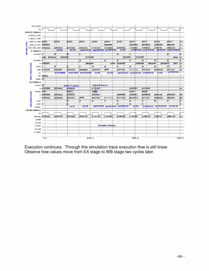
Execution continues. Through this simulation trace execution flow is still linear. Observe how values move from EX stage to WB stage two cycles later.

- 67 -
Execution continues linearly. Note the behavior of the l_addr_to_mem line when the memory instructions begin. Also note the behavior of the pcstall, fd_stall, and fd_flush lines to generate a bubble in (stall) the pipeline.

- 68 -
The branch tests begin. Note behavior of brtaken line, fd_flush line, and dx_flush lines during a branch-induced flush. Branch “hiccups” occur when branching to a location that is already in the PC. PC appears not to change, but in fact it loads the same value from a new source. This is a wasteful case, but necessary to preserve correct functionality in other circumstances.

- 69 -
The branch tests continue. Approximately line 40. Note that brtaken does not pulse high in response to a jal instruction.

- 70 -
The jump-and-link is executed, and fetching begins at the new address. Note the write of the return address to R31. When jr R0 is encountered, the PC is set to zero, and the program starts over. Careful inspection of these traces will reveal that execution exactly follows the predicted execution above listed with the source code. Annotations have been placed strategically to aid in clarifying signal meanings.

- 71 -
4 Software 4.1 Development Software Several complete programs were produced to aid in the development of RISC-E hardware and software. 4.1.1 Sim Sim is a command-line simulator for the RISC-E (RISC – Extended) instruction set. It was written with two purposes in mind:
1) Enable software development for the RISC-E architecture before the architecture is implemented in hardware.
2) Provide a means of testing for the RISC-E architecture by providing a method to debug test programs before execution on the RISC-E processor.
The use of sim has allowed parallel development of hardware and software, effectively reducing the time required to generate meaningful programs in the RISC-E instruction set. Test programs and demonstration programs were developed and debugged without concern for potential hardware malfunctions. Sim was written in C/C++ for Win32 machines. Therefore, use of an MS-DOS prompt (a command-line) is required for effective use of sim. However, use of batch files (files with a .bat extension in Windows) allows effective invocation of sim from the Windows GUI. Accompanying sim is the bmpgen program, a bitmap generation utility for displaying pixel changes. The simulator itself does not implement pixel-change information—it instead prints a message to stdout or a specified output file that characterizes each individual pixel change. The bmpgen program can convert the sim output to a meaningful Windows bitmap image (with a .bmp extension), which can in turn be displayed by any graphics program, such as Windows Paint. For further information on bmpgen and its syntax, see the appropriate section of this manual. Effective use of sim and bmpgen enables programmers to emulate actually running a program on the RISC-E processor, but also provides helpful debugging and tracing tools to speed the development process.

- 72 -
4.1.1.1 Syntax of sim Correct syntactical usage of sim is essential to using the program effectively. The correct syntax is:
sim <input file> [output file] [switches] Note that arguments enclosed in < > are required, but arguments enclosed in [ ] are not, and order of arguments is checked. Thus:
sim myfile.asm myfile.out and
sim test1.asm –v +r +m
Are valid invocations of sim, but
sim –v test1.asm is not, as a switch is listed before the input file (test1.asm). Specifying an output file for sim has the same effect as redirecting sim’s output to a file using the > operator in MS-DOS. Thus:
sim stdlib.asm –v +r > stdlib.out and
sim stdlib.asm stdlib.out –v +r
are equivalent executions of sim. A complete list of switches for sim: Switch Description +h Display syntax message. +r Dump register file to output stream after execution. +m Dump non-zero memory locations to output stream after
execution -v Verbose mode off—Does not echo code to output stream. +i Instruction Memory Fill—Fills instruction memory with
0xFFFFFFFF to simulate presence of instructions at those memory addresses.
+vgasilent Does not print pixel manipulation information to output stream. Useful for diagnosing infinite loops.
+fast Disables long loop waits for I/O (see instruction set and I/O Section below). Recommended only for pixel manipulation-intensive programs.
Invoking sim without arguments or with improper arguments will also display the above-mentioned list of arguments and switches.

- 73 -
4.1.1.2 Programming with sim The simulator was designed to emulate a RISC-E architecture’s environment as accurately as possible. Therefore, capabilities and limitations that exist in hardware also exist in sim, with some exceptions. The rules of language syntax for sim are those one might expect for an assembler—illegal opcodes and registers, undefined labels, and inappropriate offsets will be flagged as errors. E.g.:
The response to an illegal opcodes
In the example above, the first four instructions are valid—the opcodes are defined and the arguments are correctly specified. However, the RISC-E architecture does not include a ‘div’ instruction, hence sim’s response of “Unknown opcode.” Similar responses exist for other errors, such as those listed above. Note that errors in syntax abort the simulation—to continue would be to return ambiguous results. The memory system in sim also faithfully represents the RISC-E architecture—the acceptable addressable range is 0x00000 to 0x3FFFF (an 18-bit range, the logical range of a RISC-E system). Memory accesses out of the acceptable range are handled by the simulator in the same manner of actual hardware—the upper 14 bits are simply truncated. Thus, a read from address 0x1247FFFF will read from memory location 0x3FFFF. It is important to note that sim does not assemble or locate code. Therefore, reads from “instruction memory” will not return valid instructions, and nor will writes to “instruction memory” in any way affect execution. The +i option exists to fill “instruction memory” with 0xFFFFFFFF, if it is desirable to flag it in this way. In this manner, sim is not faithful to the RISC-E architecture—instruction and data memory are effectively separate in the sim environment, but not in the true RISC-E system.

- 74 -
4.1.1.3 Instructions in sim <instruction> [arguments] The following is a brief listing of recognized instructions in sim: (For a more comprehensive listing, see the RISC-E Programmer’s Manual) Instruction Arguments Description (RTL if applicable) add regd rega regb Addition: D � A + B sub regd rega regb Subtraction: D � A – B inc regd Increment: D � D + 1 dec regd Decrement: D � D – 1 mul regd rega regb Multiply: D � A * B
Note: Multiplies lower 16-bits of A and B to produce a 32-bit result.
and regd rega regb Logical AND: D � A & B or regd rega regb Logical OR: D � A | B not regd rega Logical NOT: D � ~A xor regd rega regb Logical XOR: D � A ^ B lw regd regaddr
imm_dec9 Mem: D � memory[regaddr + imm_dec9]
sw rega regaddr imm_dec9
Mem: memory[regaddr + imm_dec9] � A
svga rega Pixel manipulation, see I/O Sub-Section push rega Stack: TOS � A, R30 � R30 – 1 pop regd Stack: D � TOS+1, R30 � R30 + 1 sl regd rega regb Logical Left Shift: Reg B contains shift
amount. srl regd rega regb Logical Right Shift: Reg B contains shift
amount. sra regd rega regb Arithmetic Right Shift: Reg B contains
shift amount. ror regd rega regb Rotate Right: Reg B contains rotate
amount. rol regd rega regb Rotate Left: Reg B contains rotate
amount. lui regd imm_hex16 Load Upper Immediate:
D � {UH_D , imm_hex16} lli regd imm_hex16 Load Lower Immediate:
D � {UH_D , imm_hex16} breq rega regb label Branch to label if A = B brgt rega regb label Branch to label if A > B brlt rega regb label Branch to label if A < B brchar label Keyboard polling branch, see I/O Sub-
Section brpix label Pixel polling branch, see I/O Sub-Section brvid label Character polling branch, see I/O Sub-
Section br label Unconditional branch nop No-operation

- 75 -
jr regaddr Jump to value specified by register jal label Jump to label (unconditional) Recognized instructions and their functions
Abbreviation Definition rega, A rega is a source register, A is its content regb, B regb is a source register, B is its content regd, D regd is the destination register, D is its content (sometimes
also used as a source) regaddr regaddr is a source register containing an address imm_dec9 A decimal user-specified immediate value, bounded by:
-2^8 < imm_dec9 < 2^8 –1 (2’s complement) imm_hex16 A hexadecimal user-specified immediate value. This may be
replaced by a positive decimal value if it falls within the range 0x0000 to 0xFFFF. Otherwise, it must be specified as D3D2D1D0h where Di is a valid hex digit. Omitting the terminal h may yield undesired results, as sim will attempt to cast this number as a decimal value.
UH_D The upper 16 bits of D (D is specified above) TOS Top-Of-Stack, or memory[R30] label A user-defined label. See Labels below. A list of abbreviations and their meanings
4.1.1.4 Registers and Arguments Registers may be specified by any of three methods:
R<number> r<number> $<number> The range of <number> above is 0 – 31, specified in decimal. There are four special-purpose registers in the RISC-E architecture. They are accessed normally as a general purpose register, but also serve the following purposes: Register Remarks R0 Register is always value 0x00000000. R29 Register is dedicated to I/O. See I/O Sub-Section R30 Stack Pointer, also usable as a general-purpose register if not
employing a stack. R31 Return-address register. jal instructions place the return
address in this register—ideally the system will eventually execute jr R31 to return.
Special purpose registers
Most instructions require one or more arguments. Argument type varies by instruction. The user should consult the tables above for argument requirements of a particular
- 76 -
instruction. Multiple arguments may be delimited by whitespace (excluding the newline character) or commas. The following are all acceptable instructions: add R1 r2 r3 xor $6, $7, $8 breq r1 $0, XLABEL 4.1.1.5 Labels Labels are defined by any line starting with a colon ( : ), followed by up to seven alphanumeric characters. Labels are referenced by their name only—do not include the colon when referencing a label. Labels are case-sensitive in sim. Thus:
:ULAB1 br ULAB1
Is an infinite loop, but :ULAB1 br :ULAb1 generates an error. Labels have the following restrictions:
• Labels may not exceed seven characters in length (excluding the colon) • The colon is only used only to declare a label, not to reference it. • A label may not begin with any valid hexadecimal character (eg 0-9, A-F, or a-f)
and may not start with R, r, or $. • For assembler compatibility, labels may not appear on the same line as
comments. 4.1.1.6 Comments and Whitespace To aid in code readability, comments may be inserted in a source file to highlight key sections or explain complex algorithms. All comments recognized by sim begin with a double forward-slash, //. The semantics of the //-type comment are identical to that of popular programming languages, such as C or Java. These comments may be placed anywhere in the source file, with the following exceptions:
• Lines consisting of only comments and whitespace must begin with //, and may not begin with whitespace.
• For assembler compatibility, labels may not appear on the same line as comments.
Note: While C-style // comments are supported by sim, block-comments of the /* */ type are not supported. Whitespace (both horizontal and vertical) may be used arbitrarily by the programmer to improve code readability without affecting execution of sim. 4.1.1.7 Reserved word stop STOP (case insensitive) is a reserved word in sim. It exists to ensure 100% compatibility with the RISC-E assembler, which requires stop at the end of a source file. Should a program in execution encounter stop, execution will cease normally.

- 77 -
STOP should only be placed at the end of source file—placing stop in the middle or beginning of a file will cause a miscalculation of all branch/jump addresses that cross the stop reserved word. 4.1.1.8 I/O (Input / Output) The RISC-E system utilizes a VGA output device and a (PS/2) keyboard input device. The programmer may access these devices to perform I/O in the course of program execution. There are three methods of I/O in the RISC-E architecture: keyboard input, character output, and pixel output. The simulator will directly support both keyboard input and character output, and will support pixel output with the use of the accompanying bmpgen program. Keyboard input: To read a character from the keyboard, the programmer need only read a value from register R29. R29 is a dedicated I/O register—the lower eight bits of this register represent the last key depressed on the keyboard (in ASCII). If no ASCII code exists for a key, and its code is not otherwise defined in the table below, then the code visible in R29 will be 00h on a true RISC-E system. In sim, its code will be determined by the C getch() function call. In this way, sim is not true to the RISC-E architecture, and thus the user should only attempt to use sim when expecting defined inputs. Key R29 Code Key R29 Code � 38h RETURN 0Ah � 32h ENTER 0Ah � 34h � 36h
Nonstandard key codes
It is important to note that R29 may be read at any time, though its value may not always be meaningful. If the user has not depressed any key, then the value of R29 should not be considered valuable input. Thus, the programmer must first poll the keyboard interface using the brchar instruction to determine if a key has been pressed. (brchar is taken if the value in R29 has not yet been read.) To simulate this behavior, sim actually implements a counter that is initially random and decrements with each successive brchar instruction. When this counter reaches zero, sim will initiate a key request calling C’s getch() function. The getch() function returns the pressed character (without echoing to the screen) and that value is then stored in R29, presumably to be read in subsequent execution. As mentioned above, use of getch() limits sim’s ability to correctly emulate the RISC-E keyboard interface. However, for most user inputs sim’s performance matches that of hardware. Alphanumerics, whitespace, and most symbols will function identically in RISC-E and in sim.

- 78 -
Character Output: Writing a character to the screen in the RISC-E system is equally as simple as reading from the keyboard. Again, register R29 is used to interface with the I/O system. Writes to R29 will initiate character output, if the VGA controller is ready to accept a new character. The value written into R29 will be truncated to its lower eight bits, which will be interpreted as an ASCII character by the VGA controller. For polling purposes, branch instruction brvid will be taken when the VGA controller standing by for a new character. As in the case of character input, it is highly recommended that the programmer make careful use of the brvid instruction to ensure that R29 is written only when the VGA controller is ready. Failing to poll correctly in hardware will result in the character write request to be ignored. Failing to do so in sim will generate a warning printed to the designated output file (usually stdout):
Response to a non-polled R29 write
Character output in sim employs the C function putc(). As a result, sim also is unable to exactly match the character-output behavior of the RISC-E system, as putc() will print some symbols that are not recognized in the RISC-E architecture. Additionally, the VGA controller can also accept commands via the R29 interface that cannot be implemented in sim (for details, consult the VGA Controller documentation). Finally, MS-DOS command-lines will scroll output as more and more characters are printed to the screen, but there will is no such scrolling action in the RISC-E character output system—instead the user must erase the screen by writing backspace characters followed by space characters. The backspace/space requirement is modeled correctly in sim.

- 79 -
Pixel output: The RISC-E architecture also allows the user to perform individual pixel manipulations. As in the case of character output and keyboard input, a polling instruction exists to facilitate timing of pixel manipulation requests. This instruction is brpix—it is used identically to that of brvid and brchar. Branch brpix is taken if the VGA controller is ready to accept a pixel manipulation. Unlike character I/O, RISC-E affords a separate instruction to pixel manipulation, the svga instruction. Note that svga denotes “send to VGA,” and does not reference the common acronym SVGA. The svga instruction takes one register as its argument—the pixel manipulation data is entirely encapsulated in that register. To reference how to format pixel data, refer to the RISC-E Programmer’s Manual or the VGA Controller documentation. Pixel manipulation is not completely supported by sim, but the bmpgen program can be used to render sim’s pixel-manipulation output into a viewable format (see 4.1.1.9 bmpgen). However, sim will recognize when a successful pixel manipulation has occurred, and will print a message to its specified output stream:
Response to four pixel outputs
For programs that are pixel-manipulation intensive, it is recommended that the +vgasilent and +fast command-line options be employed. When sim is invoked with these switches, no pixel manipulation information will be printed to the specified output stream, and the polling requirements of the simulated output device will be relaxed substantially. Execution time for these programs will be dramatically reduced.

- 80 -
4.1.1.9 bmpgen for Viewing Pixel Output It is possible to view pixel manipulations generated by a program once execution has terminated by using the bmpgen program. bmpgen will convert the pixel manipulation data generated by sim into a viewable (bitmap, *.bmp) format. The output bitmap always has width 256 and height 256 (pixels). Pixel manipulations outside of these dimensions are not visible using bmpgen. The background color of this bitmap is black—therefore writing black-colored pixels will not be visible after using bmpgen. The colors that are generated by bmpgen are in general not the same colors that will appear on a RISC-E system—bmpgen is intended to show pixel patterns, not true pixel colors. However, the colors white (FFh or 255 decimal) and black (00h or 0 decimal) are accurately modeled in bmpgen. To syntax of bmpgen is:
bmpgen <input file> <output file> eg
bmpgen pixels.out pixels.bmp
Both the <input file> and <output file> arguments are required. The result of the execution (in <output file>) is a bitmap image. The <input file> format is ASCII text, though it is expected that this file will be an output file from an invocation of sim. The bmpgen program will examine this file and look for pixel-manipulation statements like those shown in the example above. It will then modify the output bitmap accordingly. Therefore, only the most recent update to a pixel will be visible. Note: The +vgasilent switch should not be used when generating an input file for bmpgen. However, the use of +fast is highly recommended.
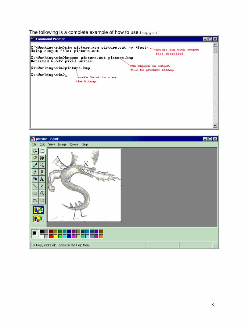
- 81 -
The following is a complete example of how to use bmpgen:

- 82 -
4.1.1.10 Files sim.exe The executable form of sim bmpgen.exe The executable form of bmpgen header A required data file for bmpgen sim.cpp Source code for sim instrs.inc Source code for sim stdlib.asm A collection of useful functions dobitmap.bat An MS-DOS batch shell for streamlining use of sim+bmpgen

- 83 -
4.1.2 AssemblerT The first version of AssemblerT was designed using the Jflex and Yacc tools provided to us by the Computer Science department of UW – Madison. Unfortunately, using these tools became impractical as it required nearly 20 separate Java files and was cumbersome to transport between platforms. The second and currently used version was written in Java but spans only one file, making portability a plausible reality. AssemblerT must be run using the Java virtual machine under on a Unix machine: java AssemblerT <filename> AssemblerT then creates two separate files, one called <filename>.out and one called <filename>.xes. The first file is used for simulation with Modelsim and is written in the format @00000 0000 0400 3540 1258 where 00000 is the starting address of the of the compiled program and the instructions are listed in little-endian form, i.e. the first instruction is actually 04000000 and the second is 12583540. The second file the assembler produces is an xes file, which is used to run programs on the FPGA. It is written in the form + 10 00100000 FF FF 50 F0 00 03 51 F0 00 01 51 08 61 00 50 08 + 10 00100010 00 00 50 10 00 01 51 10 44 01 90 00 41 00 40 08 + 10 00100020 40 02 90 00 00 9A 71 F8 50 00 50 08 80 00 51 10 + 10 00100030 00 10 50 10 C6 00 12 18 00 C9 50 18 44 00 90 00 The initial “+ 10” is required syntax for the xes form. The next eight digits are the hexadecimal address for the instructions that follow, and the last string of digits are the actual instructions. The instructions are listed in little-endian form per 16 bits, but big-endian form per byte. To illustrate, the first instruction is 50F0FFFF and the second is 51F00003, etc. The syntax of the input file is flexible, with one exception. The keyword stop must appear on the last line of the program. This signals the assembler to add any nop’s to the end of the file in order to fill in the last few lines of the xes file and to close the output streams so that the files can be read. Each line of the xes file holds four instructions, so if the input file doesn’t have a number of instructions that is divisible by four, the assembler adds nop’s until it is. Punctuation in the instructions is optional, thus

- 84 -
lw $1 $6 0 lw $1, $6, 0; will both compile to the same instruction without errors. Registers can be specified in one of several ways. For ease of use, AssemblerT accepts “$”, “r”, or “R” as the initial character for designating a register. Offsets can be specified in one of three ways. The first way is simply with a decimal number. The second is by a hexadecimal value which must be followed by an “h” or it will be interpreted as a decimal value. The final way to specify an offset is with a label. Each label stores the value of the instruction immediately following it so lw $1 $0 label would load the instruction at “label” into register 1, if the instruction at “label” is within the requisite 9-bit range. AssemblerT can put code into one of two segments. The “.text” and “.data” directives indicate two different locations to place the instructions in the xes file. The .text segment starts code at hexadecimal location 100000 and the .data directive starts code at 15000 hex. Knowing these values, the programmer can create global variables in his program that require no runtime setup. By loading a register with the value 15000, he can easily access the data segment of the code to load from and store value to a predefined initialized block of code or data. The data segment also has the advantage that it will never be executed, as the processor begins reading at address 100000 and in general never reaches the data segment for execution. Values in the .data segment (and the .text segment as well, but as those instructions will be executed, the programmer is advised to use this format only in the .data segments) can be specified simply by typing a number in either decimal or hexadecimal. For example, .data 015 12345678h would load beginning at address 150000 the values 15 and 12345678h. Numbers declared in this segment must be at least three digits long. For instance, if the programmer wants to load the number 1, he would need to specify the value as 001. In order to accomplish all this, the assembler uses a two-pass system. On the first pass, it ignores all instructions but labels and places their values into a hashtable. There are two public integers in AssemblerT, linenumber and blanksandlabels. As the assembler make its first pass, it checks for empty lines, lines that begin with “//” (the

- 85 -
designator for a comment), .data and .text directives, and labels, which it reads and then increments blanksandlabels. Everything else it assumes is executable code and increments linenumber. A label is specified by a colon followed by a string of characters which designate the label. When the assembler reaches a label on the first pass, it loads the name of the label into the key field of a hashtable and it loads the line number in the predefined Integer class form into the data field of the hashtable. There is a second hashtable in the assembler that is currently not being used, but it holds the label name in the key field and 0 for .data and 1 for .text in the data field. If the functionality of this had been achieved, the programmer would have been able to declare labels in the .data segments in order to define global variables. This feature was never completed as our instruction set does not have enough bits in the offset field of load words and store words to bridge the gap between 100000h and 150000h. In the first pass, the programmer may encounter an error message if a label has been defined and the user tries to define the same label a second time: Label <labelname> on line <linenumber> has already been used. The second label will be ignored and the compiler will continue running, but the output may not be what the user expects as all branches, jumps, loads and stores will use the value of the first label when he might have been expecting the use of the second label. There is a bug in AssemblerT in the first pass. It has to do with the String Tokenizer as it goes through the program the first time. If the label being declared is followed by a comment, the entire line will be entered into the hashtable as the key. For example, :loop //iterates through the entire array lw $1 $7 0 inc $7 brlt $7 $9 loop If this code is assembled, “loop //iterates through the entire array” will be the key in the hashtable on the first pass and the programmer will get an unexpected “Syntax Error Line <linenumber>: Invalid Offset Value” on the brlt $7 $9 loop. This bug is easy enough to get around once it’s known. In order to avoid such an error, simply move the comment up a line so the new code looks like this: //iterates through the entire array :loop lw $1 $7 0 inc $7 brlt $7 $9 loop
- 86 -
Now that there is nothing following the label, only the text which is intended to be entered into the hashtable will be entered, so when this code assembles, no unexpected errors will be encountered. The second pass is where the actual assembly occurs. Two files are opened which, upon completion of assembly, will be deleted. Assembler1.out and Assembler2.out are created in order to store temporarily the values of the .data and .text segments. These two files are then concatenated into the output file <filename>.xes. The assembler uses a String Tokenizer in order to read in one token at a time. The first token read can be one of many things. If it’s the opcode for an instruction, the assembler enters that state. From there it anticipates what should be coming next and if it doesn’t receive it, it will print an error message. For example, if the first token was a load word, but the next token was a label, the assembler would print the error message Syntax Error Line <linenumber>: Invalid Register Name Or if the first token was a load word, and the next three tokens were registers (The third argument to a load word instruction is an offset) then the assembler would print the error message Syntax Error Line <linenumber>: Invalid Offset Value When a label is used in the code as an offset value, its first read in a try block. The assembler reads the last character of the string. If it is an “h” it interprets the offset as a hexadecimal value, but if the last character in the string is not an h, it tries to parse it as a decimal value. If this fails, a NumberFormatException will be thrown, which is then caught by the catch block. The catch block then searches the hashtable for a corresponding label, and if one is found, uses the data attached to the key as the offset. Otherwise it prints the error message listed above. Each opcode goes through its own assembly process. There is a public String field in AssemblerT called instr which holds the binary string of digits of the assembled instruction thus far. The first data entered into instr is the opcode and mode bits of the instruction being compiled. Then each instruction differs from the others. R-type instructions take three register inputs. Each register token is read in, the 5 bit register value is taken from the string and placed in consecutive order in instr. When an R-type instruction is finished, instr is a 32 bit binary value represented as a string. When a load is compiled, instr takes the opcode, mode, two registers and an offset and concatenates them together. In general this is how the assembler puts instructions together with a few exceptions. In a store word instruction, the operands are in reverse order from the order that they’re assembled. So instr takes the opcode, mode, the second specified register, the first specified register, and the offset and concatenates them together in that order. The increment and decrement instructions only take one register as an operand, but it duplicates that register, so the final value of instr is the opcode, mode, specified register, and then specified register again. When an instruction takes up less

- 87 -
than 32 bits, like an increment or decrement does, the remaining bits are filled with zeros. At the end of each opcode’s assembly block, there is an if statement that checks to see if linenumber divides evenly by four (linenumber mod 4 equals zero). There is another public field in AssemblerT called machinecode. When an instruction finishes assembling and instr contains 32 bits, instr is added onto the end of machinecode. So if linenumber mod 4 equals zero, that means that machinecode contains 128 bits of data. This is a full line in an xes file so the assembler calls the method outMacineCode to print machinecode to one of the two output files. This method breaks machinecode into substrings which it then turns into hexadecimal values and outputs them to the output file with the proper spacing and other formatting. If any line has one of the two errors listed above, it is not outputted to the temporary files. Instead, linenumber is decremented and instr is set to null so in the output file it appears as if the offending instruction never existed in the input file. This can lead to undefined behavior in the users program as this instruction may have been key in correct implementation of the program. The user is strongly advised not to use code outputted by AssemblerT if any errors were found in the input file. If a token is omitted completely and the assembler looks for one, an unhandled NoSuchElement exception will be thrown. If this occurs, the assembler will not finish assembling the input file and will therefore not close the files for reading and writing. In this event, both output files will be blank. In order to combat unanticipated errors such as the one listed above, the assembler has a debug feature. In the source code there is a line commented out System.out.println(s1); which when uncommented will print each opcode of the input file. When an error occurs, the offending instruction will be the one that immediately precedes the error. With this feature turned on, it is easy to find erroneous instructions and fix the problem so that errors will not be encountered during the next assembly of the input file. When the assembler encounters a comment, it simply ignores the line and increments blanksandlabels. The field blanksandlabels is zeroed between the first pass and the second. The purpose of this field is to report error messages in a meaningful way. When an error message is reported, linenumber and blanksandlabels are added together to report the line of offending instruction. When the assembler encounters a label on the second pass, it increments blanksandlabels and ignores the rest of the line. If the next token the assembler reads is a .data or .text directive several things happen. There are six public fields in AssemblerT: textlinenumber, datalinenumber,

- 88 -
datamachinecode, textmachinecode, textgroup4line, and datagroup4line. When a new directive is reached, a field, lastblock, is checked. If lastblock equals one, then the last block was a .text block. If lastblock equals zero, then the last block was a .data block. All fields are initialized so that if the programmer chooses not to use the .data or .text directives, all code will be assembled into the .text address location. This means that linenumber is initialized to zero, lastblock is initialized to 1, machinecode is initialized to an empty string, and group4line is initialized to 00100000h. Depending on which block the assembler was just in, it stores the values of linenumber and machinecode into the appropriate fields, data or textlinenumber, and data or textmachinecode. When these current values are stored away into fields where they won’t change until we reenter the current block type, we load the values of the corresponding directive into linenumber and machinecode so as to pick up from where the assembler left off last time it was in this block type. This allows the programmer to switch back and forth at any time between .data and .text segments and have the output file return as if all .data and .text segments had been written together. For example, .data 005 FEDCBAh 1943 .text lli $7 5000h lui $7 0001h lw $1 $7 0 lw $2 $7 1 add $1 $1 $2 .data 1776 2003 .text add $1 $1 $2 would output an xes file with the following form + 10 00100000 50 00 50 38 00 01 51 38 C0 00 80 09 C0 01 80 11 + 10 00100010 44 00 00 08 44 00 00 08 00 00 40 00 00 00 40 00 + 10 00150000 00 05 00 00 DC BA 00 FE 07 97 00 00 06 F0 00 00 + 10 00150010 07 D3 00 00 00 00 40 00 00 00 40 00 00 00 40 00 where the .data and .text segments have been conglomerated into single segments. Here it is evident that the lines are filled with with nop’s (00 00 40 00) when the lines are not evenly divisible by four. The initial address in the xes file is controlled by a field called group4line. This field is incremented every time that outMachineCode is called and when the segment changes, the values are stored and loaded into textgroup4line and datagroup4line. These fields

- 89 -
are then turned into hexadecimal values and concatenated with one zero in order to produce the correct address. When the assembler reaches the stop command, several things occur. Initially, it saves the values of linenumber, machinecode, and group4line into the corresponding fields for the current code block. Then the assembler loads the values of the data fields into the current fields and checks to see if the last instruction was evenly divisible by four. If not, it concatenates nop’s onto the end of machinecode until this condition is met and then calls outMachineCode. Then it loads the values of the text fields into the current fields and checks to see if the last instruction in the text segment was evenly divisible by four. If not, it concatenates nop’s onto the end of textmachinecode until textlinenumber is divisible by four and then calls outMachineCode. When both of these processes have been completed, the assembler closes the two temporary output files as well as the output file of the form usable by Modelsim. It then opens the temporary files for reading, and concatenates them into one file, specified by <filename>.xes. When this process is complete, the temporary files are closed for reading and deleted, while the xes file, which now contains the proper data in the proper format, is closed for writing. AssemblerT then calls System.exit(0) which terminates the Java program and the assembler has finished running. The two output files now contain the correct representation of the input file. There are several public methods in the AssemblerT file. Most of them have to do with creating offset values of the proper length. There are methods to create immediate values of 32, 18, 16, 14, and 9 bits in both binary and hexadecimal values. Each method is very similar to the others. A string is passed in to the method which represents the offset token received from the input file. The integer is then parsed as either a decimal number or a hexadecimal number depending on which method the assembler calls based on whether or not the last character in the string is “h”. This integer is then turned into a binary string of digits. The length of the string is then checked against the length that is to be returned by the method. If the length of the string is greater than the return length and the number is not negative (if the number is negative Java will automatically return 32 bits sign extended) then an error message will be printed Warning Line <linenumber>: Offset Too Large, Truncating The assembler will continue to run in this case but the offset will be truncated to the lower order bits of the size which is to be returned by the given method. If the string is not long enough, zeros are concatenated to the beginning of the string until the length is correct. And if the length happens to be correct without any alterations, then the string is simply returned. AssemblerT was a very influential development tool for designing programs to run on the processor. After learning its nuances, the assembler is an easy to use and flexible program that allows a quick transition between writing code and testing it on the FPGA.

- 90 -
4.1.3 Assembly Text Generator convert.exe generates code to print text on the RISCE architecture. The text is taken from a user specified input file and the generated code is put into a user specified output file. Usage is as follows: convert <input> <output> [-r] [-o] The flags are optional and have function as follows: default: All carriage returns in the input file are not put in the output file code. Any
lli that reloads the same value the register R1 has in it is not put in the code.
-r: Puts carriage returns into the output code. -o: Does not remove repetitive lli instructions from the output code. Known issues to be aware of: -Input and Output files must be specified.
-Output file is in ASCII format, but newlines are specified by only a newline character (notepad expects a carriage return then newline) unix and most other windows text editors will read the file fine. -Most ASCII characters you can type using a simple text editor should be interpreted correctly by the converter, but some characters may mess up the output file if you were to use a hex editor to put them directly into the file. For example, if the converter comes across a backspace character in the input file, the comment that is supposed to describe the character being loaded would contain only one slash, and would therefore not be a comment. -The XPUTC function from stdlib.asm must be included in the file the generated code is put into, because the generated code makes multiple calls of the function.
Examples: Program usage: convert input.txt output.asm convert infile outfile -r convert start.txt start.asm -o -r IO: Input: SS Output: Default: lli R1 83 //S jal XPUTC jal XPUTC //S lli R1 10 //newline jal XPUTC

- 91 -
-r: lli R1 83 //S jal XPUTC jal XPUTC //S lli R1 13 // jal XPUTC lli R1 10 //newline jal XPUTC -o: lli R1 83 //S jal XPUTC lli R1 83 //S jal XPUTC lli R1 10 //newline jal XPUTC -o -r: lli R1 83 //S jal XPUTC lli R1 83 //S jal XPUTC lli R1 13 // jal XPUTC lli R1 10 //newline jal XPUTC

- 92 -
4.1.4 Bitmap To XES-16 Converter The bitmap to XES-16 converter was developed to aid in the debugging of the VGA unit. The implementation of the VGA unit at the time of development only displayed the contents of the right SRAM, so it was necessary to initialize that SRAM so the color palette of the VGA unit could be properly tested. There are two versions of the program bitmap.exe is for 256 color bitmaps and bitmap1.exe is for 24-bit color bitmaps. Bitmap1.exe results in more accurate color mapping than the 256 color version. This is because the program uses an algorithm to map the 24-bit colors into 8-bit colors the same way the color palette of the VGA unit does, the program also rounds the color to the nearest displayable color the VGA unit supports to keep the colors as accurate as possible. The 256 color version simply strips the header file of the bitmap and does not attempt to match the colors to the color table defined in the header, this leads to even more inaccuracy in the color that is displayed by the monitor. The program expects as input a bitmap file that is 512x480. If the input file is not this size the image from the SRAM will be distorted. The XES-16 file that is written into the right SRAM for the VGA unit to display contains all the data in the original bitmap, but the VGA unit only displays in resolution of 368x480, so the right side of the image is not displayed on the monitor. The monitor distorts the 368 pixel width of the output, so that it is necessary to shrink the original bitmap by 67% horizontally, if this is done the proper aspect ration will be displayed on the monitor when the bitmap is displayed by the VGA unit. This tool allowed us to track down many problems in the VGA unit including failure to initialize the color palette correctly and an off by one error with the timing of the blanking signal. It should be noted that clever creation of an input file with a hex editor could be used to initialize the right SRAM to any data one wanted to. bitmap.exe and bitmap1.exe usage: bitmap <input bitmap> <output XES>

- 93 -
4.2 Board Software All Board Software source files can be located in Appendix 3. Below are discussions of individual programs. 4.2.1 Demonstration Programs Demonstration programs represent complete or near-complete works that effectively demonstrates the capabilities of the RISC-E architecture. 4.2.1.1 Shell The Shell program is a basic operating system for the RISC-E architecture. It has two primary functions:
1) Provide a text-based user interface, similar to but much simpler than common Unix-style shells (eg. bash, tcsh)
2) Provide a means to execute other programs and then return to Shell when the program completes execution.
To accomplish these functions, it has two modes of execution. Interactive mode entails all user I/O functions—listing the programs in memory, changing text colors, etc (see below). Dispatch mode begins when a program has been selected by the user—when in Dispatch mode Shell makes any necessary preparations (eg. preserving registers, setting up the stack, etc) before actually transferring execution to the selected program. 4.2.1.1.1 Interactive Mode The Shell program runs in Interactive mode for most of its execution time. It is during Interactive mode that prompts are printed, user input is read, and commands are processed.
There are three built-in commands in shell: l List programs in memory: This command
lists the names and associated commands of all programs available for Shell to execute.
C Clears the screen. Also sends the cursor to the home position (upper left). Note that Shell will automatically execute “clear” should the cursor approach the bottom of the screen.

- 94 -
T <HEX><HEX><HEX><HEX> Text change: This command allows the
user to specify a new foreground color and background color for text output. <HEX> indicates a hex value, 0-F. The first two hex values represent the background color, the second pair corresponds to the foreground color. IE t FF07 changes the background color to white (FF) and the foreground color to blue (07).
The user may also execute programs from Interactive Mode by beginning a command line with a program’s command character (using l above prints a list of programs and their command characters). 4.2.1.1.2 Dispatch Mode Shell enters Dispatch Mode when a program’s command character has been received. Shell then performs any required initialization operations that the target program may require. After initialization is complete, Shell then jumps (via a jal instruction) to the selected program. It is expected that upon termination, the target program will execute jr R0 to return to Shell. At the time of completion of this project, two target programs were implemented in Shell—“aaa flood” (see the Test Programs section for a discussion of “aaa”) and “Etch-a-Sketch.” Other programs could be easily added to Shell, time permitting—the only requirement for 100% Shell compatibility is to provide some mechanism of returning control to shell on program termination (usually, jr R0).
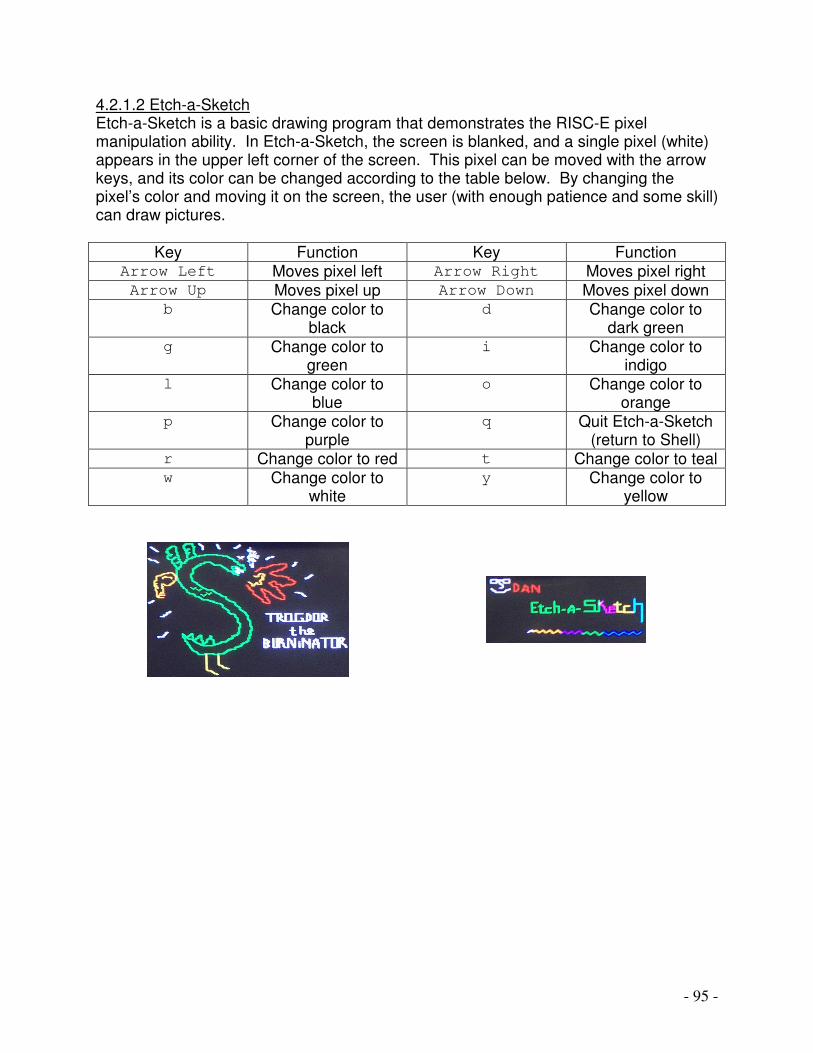
- 95 -
4.2.1.2 Etch-a-Sketch Etch-a-Sketch is a basic drawing program that demonstrates the RISC-E pixel manipulation ability. In Etch-a-Sketch, the screen is blanked, and a single pixel (white) appears in the upper left corner of the screen. This pixel can be moved with the arrow keys, and its color can be changed according to the table below. By changing the pixel’s color and moving it on the screen, the user (with enough patience and some skill) can draw pictures.
Key Function Key Function Arrow Left Moves pixel left Arrow Right Moves pixel right Arrow Up Moves pixel up Arrow Down Moves pixel down
b Change color to black
d Change color to dark green
g Change color to green
i Change color to indigo
l Change color to blue
o Change color to orange
p Change color to purple
q Quit Etch-a-Sketch (return to Shell)
r Change color to red t Change color to teal w Change color to
white y Change color to
yellow

- 96 -
4.2.1.3 Fire Fire uses a classic fire simulating algorithm which generates a random number and stores it to the bottom row of a buffer. It then calculates the weighted average of the pixels around it to give it a blurring effect. In order to calculate the current pixel, the program reads the pixel above, one to the left, one to the right, right one and down one, left one and down one, and down one three times and shifts by 3 to get the average of all the pixels read. The pixel directly below is read three times so as to weight the fire in the downward direction. This has the effect of making the fire burn taller. If the averaged value of the current pixel is less than 127 out of 256, the value of pixel is rounded to zero in order to create more dramatic changes in the fire and will cause the fire to fade out and eventually die. As the program iterates, the fire appears to move as new random values are added and blurred into the already existing picture. Random numbers were generated using a software linear feedback shift register. In order to make the fire more dramatic we implemented a VGA unit which displays 8 bits of green and 0 bits of red and blue. This gives us a more gradual blurring of the fire in a greenscale environment.
Screenshot of greenscale fire
4.2.1.4 PONG! 4.2.1.4.1 Overview Pong is a remake of the classic arcade game from the 80s written in our assembly language and run on our processor. Initially, the program blanks the screen using the XBLANK function of the standard library. This draws a black square and recursively calls itself, decrementing both the x and y values over each iteration. Then
PONG! Press A Key To Continue
is displayed on the screen in the center and the program waits for a key to be pressed. Once a key is pressed, the game begins. First the walls are drawn to the left and the right of the playable board area. Following that, the paddles are drawn, and finally, the ball. As the program progresses, a timed version of XGETC from standard library is called, which waits a set amount of time to see if the users press a key, and if they don’t, continues on with execution. Valid key presses include “z” (move top paddle left), “x” (move top paddle right), “,” (move bottom paddle left), and “.” (move bottom paddle right). If one of these key presses is detected, the location of the paddle is updated and the screen is redrawn. If no key is pressed, the XGETC timer counts to zero and the program continues on with moving the ball. The ball uses two registers, one holds the x speed of the ball, the other holds the y speed. If the ball hits a wall or a paddle, the corresponding speed is inverted. For instance, if the ball hits the bottom paddle, its y

- 97 -
speed would have been positive(down is positive and right is positive). When it strikes the paddle, the y speed is negated which in effect deflects the ball in the opposite direction. The game continues on like this as long as the ball encounters a wall or a paddle at each boundary. If it does not, the upper and lower boundaries are checked with the ball location. If the upper boundary is reached, that means the bottom paddle has scored a point and the register which holds bottoms score is incremented. If the lower boundary is reached, top has scored and his points register is incremented. After each point, the paddles’ and ball’s location are reset to their starting locations and the ball’s x and y speeds are reset to their initial conditions. In one implementation of Pong, the ball’s speed is changed in relation to where it strikes the paddle. Each paddle is broken into three equally sized segments. If the ball strikes the left segment of the paddle, the speed of the ball is decremented by one, if it strikes the right side of the paddle, the speed of the ball is incremented by one, and if the ball strikes the center of the paddle, the speed is unchanged. When either top or bottom’s score reaches 9, the game ends. At this time, the winner is printed to the screen
Bottom Wins! or
Top Wins!
Upon completion of a game, the program loops back on itself and resets all its values and begins the game again. 4.2.1.4.2 Development To make coding simpler and more efficient pong was developed incrementally. Each step in development was a new function that could be called by other functions to make gameplay more complex. The first step in development was drawing the ball, walls and paddles, then the welcome screen was implemented. Once these functions were debugged a function to move the paddles one pixel at a time was developed. It did this by first drawing the paddle black then redrawing them moved over one pixel, keyboard input was used to control this functionality. After moving the paddles the ball was put in motion, it was first drawn black and then redrawn the new color. Next functionality was added to cause the ball to bounce of of the walls and the top and bottom of the screen, but the ball only moved after every keypress, which made for a slow moving ball. Once the ball was bouncing around the screen a timed user input function was implemented so program execution would wait the same amount of time in between each redraw of the screen. The length of the timer took a considerably amount of tweaking to get the ball to move at just the right pong speed. After that the paddles where made to move ten pixels with each keypress so the user could keep up with the ball. With the paddles and the ball moving correctly the ball was made to only bounce off of the paddles, but a miss was not checked for so the ball would go off of the visible screen if missed and eventually come back after bouncing off of the end of memory. The next step was to

- 98 -
check for a miss and then stop the game and update the score, and after that the end of the game and a winner was checked for. The final step in making regular pong was to have the input waiting counter slowly decrement each time the ball hit a paddle, this caused the ball to speed up as the game progressed and made it considerably more interesting(we had a 10 minute volley before this was implemented!). With this version of pong complete expert pong was a relatively simple modification, if the ball hit the left third of the paddle the horizontal speed was decremented and if it hit the right third of the paddle the horizontal speed was incremented. This function caused the ball to fly off of the paddle at different angles. There are a few bug fixes in expert pong that would make gameplay slightly more enjoyable. The first is that when the ball encounters a wall with a horizontal speed of magnitude greater than 1 it partially “eats” the wall, to fix it would be as simple as checking the wall boundaries before a redraw of the ball. The other fix would be to slow the update rate of the ball when it is at an extreme angle so it is not quite as hard to hit, this would also be a simple fix because the variable speed of the ball has already been implemented.
4.2.1.5 Snake The Snake Game implemented here has some slight modifications from the original snake game, although it has the following main features:
• The snake can move everywhere on the board • The snake will die if its head touches another part of its body or if it touches the
wall or border of the board. The unique features of this snake are:
• Tt maintains the snake length to be 8 pixels at all times (easy Snake) • The movement is controllable by the arrow keys on the keyboard, that is, it
doesn’t move on its own (again, easy Snake) The scoring function of this game is based on the number of apples “eaten” by the snake. In other words, when the head of the snake touches an apple, the score is
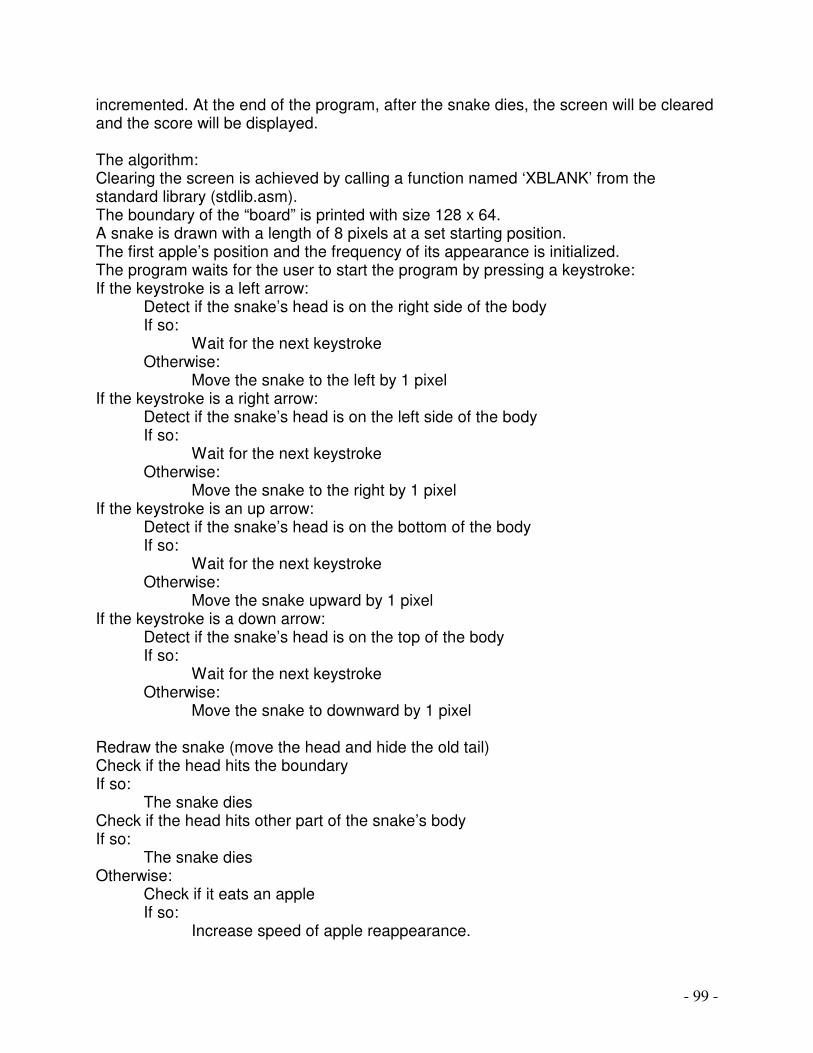
- 99 -
incremented. At the end of the program, after the snake dies, the screen will be cleared and the score will be displayed. The algorithm: Clearing the screen is achieved by calling a function named ‘XBLANK’ from the standard library (stdlib.asm). The boundary of the “board” is printed with size 128 x 64. A snake is drawn with a length of 8 pixels at a set starting position. The first apple’s position and the frequency of its appearance is initialized. The program waits for the user to start the program by pressing a keystroke: If the keystroke is a left arrow: Detect if the snake’s head is on the right side of the body If so:
Wait for the next keystroke Otherwise:
Move the snake to the left by 1 pixel If the keystroke is a right arrow: Detect if the snake’s head is on the left side of the body
If so: Wait for the next keystroke
Otherwise: Move the snake to the right by 1 pixel
If the keystroke is an up arrow: Detect if the snake’s head is on the bottom of the body If so:
Wait for the next keystroke Otherwise:
Move the snake upward by 1 pixel If the keystroke is a down arrow: Detect if the snake’s head is on the top of the body
If so: Wait for the next keystroke
Otherwise: Move the snake to downward by 1 pixel
Redraw the snake (move the head and hide the old tail) Check if the head hits the boundary If so: The snake dies Check if the head hits other part of the snake’s body If so: The snake dies Otherwise: Check if it eats an apple If so: Increase speed of apple reappearance.

- 100 -
(Decrement the apple reappearance counter) Change the coordinates of next apple Increment the score Else: Decrement the counter for the apple to appear If counter is 0 Display the next apple If the snake dies, then calls XBLANK function again and displays the score.

- 101 -
4.2.2 Test Programs In order to test the functionality of our processor we designed several test programs to observe the processors reaction to certain conditions and data dependencies. Those programs are as follows. 4.2.2.1 aaa aaa is a simple test program that increments the background color of a string of the character “a” while decrementing the color of the a’s themselves. The result of this program is a string of 2208 characters each with different text and background colors. This program was used to test both our character output function in the processor and the VGA as well as the background and text color modifications.
Screenshot of aaa
4.2.2.2 alpha Alpha was designed to test several functions of the processor all at once. Initially, it tests the character output as aaa did. “:TEST PROGRAM:” is printed onto the screen. Following that, the program reads in one line of text from the user and echoes it back. This test terminates at the newline character. The program then begins an elaborate checksum which runs through lli, lui, not, and, or, push, pop, add, xor, inc, sub, and dec. Assuming the processor successfully completes this checksum, a method is called which prints “PASS” onto the screen. If the checksum was not completed correctly a method is called that prints “FAIL” to the screen. The program then enters an infinite loop which will flood the screen with whatever happens to be in register $1 at the time to show that the program continues to execute. This program was very important in debugging our processor as it ran through most of our instructions and verified their functionality.
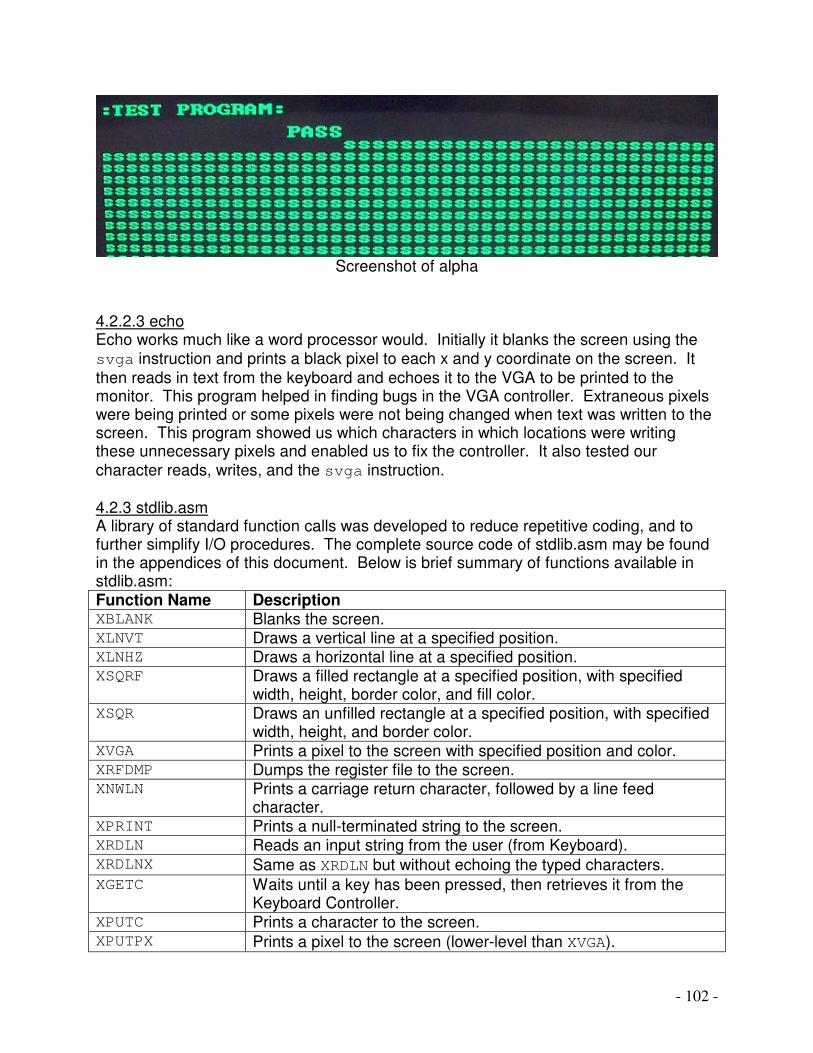
- 102 -
Screenshot of alpha
4.2.2.3 echo Echo works much like a word processor would. Initially it blanks the screen using the svga instruction and prints a black pixel to each x and y coordinate on the screen. It then reads in text from the keyboard and echoes it to the VGA to be printed to the monitor. This program helped in finding bugs in the VGA controller. Extraneous pixels were being printed or some pixels were not being changed when text was written to the screen. This program showed us which characters in which locations were writing these unnecessary pixels and enabled us to fix the controller. It also tested our character reads, writes, and the svga instruction. 4.2.3 stdlib.asm A library of standard function calls was developed to reduce repetitive coding, and to further simplify I/O procedures. The complete source code of stdlib.asm may be found in the appendices of this document. Below is brief summary of functions available in stdlib.asm: Function Name Description XBLANK Blanks the screen. XLNVT Draws a vertical line at a specified position. XLNHZ Draws a horizontal line at a specified position. XSQRF Draws a filled rectangle at a specified position, with specified
width, height, border color, and fill color. XSQR Draws an unfilled rectangle at a specified position, with specified
width, height, and border color. XVGA Prints a pixel to the screen with specified position and color. XRFDMP Dumps the register file to the screen. XNWLN Prints a carriage return character, followed by a line feed
character. XPRINT Prints a null-terminated string to the screen. XRDLN Reads an input string from the user (from Keyboard). XRDLNX Same as XRDLN but without echoing the typed characters. XGETC Waits until a key has been pressed, then retrieves it from the
Keyboard Controller. XPUTC Prints a character to the screen. XPUTPX Prints a pixel to the screen (lower-level than XVGA).

- 103 -
5 Results Maximum Clock Speed 17.5 Mhz Minimum Clock Speed 16.5 Mhz Number of GCLKIOBs 1 of 4 Number of IOBs 102 of 166 Number of Block RAMs 10 of 28 Number of Slices 2176 of 9408 Number of DLLs 1 of 4 Number or GCLKs 4 of 4 Number of TBUFs 8 of 9632 Number of Slice FFs 770 of 18,816 Overall Design Tool Effort Level 5 Overall Designer Effort Level ∞ Final Placer Score 995,287 Total Equivalent Gate Count 204,429

- 104 -
5.1 Team Contributions Dan: As team leader, Dan was involved in almost every area of the creation of the processor and the development software. His chief contributions involve the Memory Interface Unit, the Simulator and its peripheral software, the keyboard controller, the datapath, and the test programs, as well as hardware debugging. He began developing the Simulator in the first half of the semester and moved into the MIU at week 9. Then he developed the datapath and finally the keyboard controller. Test programs were developed upon completion of the processor and hardware debugging revolved around the test program’s output. Jake: The primary accomplishments of Jake include the VGA controller, the ALU, Pong, and Fire. The VGA controller went through many implementations, including a 640x480 resolution version and a greenscale version which set all 8 bits of color designation to be shades of green. Jake began at week 9 with the ALU which he quickly completed. Then his efforts were concentrated on the VGA for several weeks. In the last week, he developed the Pong and Fire demo programs. Inge: Inge’s primary accomplishments include the Hazarding and Forwarding Unit and the Control Module. She also wrote the demo program Snake. She was also the primary pre-synthesis waveform validator. At week 9 Inge began developing the Hazard and Forwarding as well as the Control Modules. Upon completion of these tasks, she began checking waveforms against expected results to verify the functionality of the modules pre-synthesis. At the end of the semester, she began developing the demo program Snake. John: John’s primary accomplishments include the initial implementation of the Register File as well as the Assembler development tool and the initial version of Fire. He also aided in hardware debugging. Prior to week 9, John began developing the Assembler, which he completed around week 10 and added and debugged features until the end of the semester. In week 10 he began developing the Register File which Dan added the finishing touches to. At the end of the semester he researched the Fire algorithm and wrote an initial version that was subsequently improved on by Jake.

- 105 -
Dan Jake Inge John Total
Architecture Overview
25% 25% 25% 25% 100%
Microarchitecture Development
25% 25% 25% 25% 100%
MIU 100% 0% 0% 0% 100% Simulator 100% 0% 0% 0% 100% Keyboard 100% 0% 0% 0% 100% Datapath 100% 0% 0% 0% 100%
VGA 0% 100% 0% 0% 100% ALU 0% 100% 0% 0% 100%
Hazard and Forwarding
0% 0% 100% 0% 100%
Control 0% 0% 100% 0% 100% Register File 10% 0% 0% 90% 100% Assembler 0% 0% 0% 100% 100%
Test Program 100% 0% 0% 0% 100% Demo Programs 25% 40% 25% 10% 100%
Pre-synthesis validation
10% 0% 90% 0% 100%
Hardware Debugging
90% 0% 0% 10% 100%
Jake Adriaens
Dan Gibson
John Schmoller
Inge Yuwono