Embed Size (px)
Citation preview

TABLE OF CONTENTS:
Organization Committee ……………………………………………........... 1
Sponsors ………………………………………………………………..….... 1
Plenary & Invited Speakers .……………………………………….………. 2
Conference Information …….……………………………………….…....... 3
Conference Venue Direction ..………………………………………….…… 5
Program Summary ..………………………………………….…………….. 6
Details of Technical Program ……………………………………………… 8
January 5, 2015 (Monday) …..…………………………………...………………… 8
Registration and Welcome Reception
January 6, 2015 (Tuesday)….…………………………………………………… 9
Session I: OLED Device and Materails I [Plenary Talk I]
Session II: Applications of Graphene & Carbon Nanostructures in organic optoelectronics
Session III A: Transistor and Memory
Session III B: Novel Device and Materials I
Session IV A: OLED Device and Materiels II
Session IV B: Novel Device and Materials II
January 7, 2015 (Wednesday) ……………………………………..................... 13
Session V: Perovskite and Organic Solar Cell I
Session VI: OLED and Organic Solar Cell
Session VII A: Perovskite and Organic Solar Cell II
Session VII B: OPV Device and Materials I
Session VIII A: OPV Device and Materials II
Session VIII B: OPV Device and Materials III
January 8, 2015 (Thursday) …………………………………………………… 17
Session IX: OPV and OLED I [Plenary Talk II]
Session X: Organic Device Interface
Session XI: OLED Device and Materiels III
Session XII: Novel Device and Materials III
January 7, 2015 (Thursday) …………………………………………………… 19
Poster Session
Abstracts of Talks …………………………………………………………...26
Tuesday (Plenary Talk I, Oral Session I-IV) …………………………………………. 27
Wednesday (Oral Session V-VIII)……………………………………......................... 56
Thursday (Plenary Talk II, Oral Session IX-XII)………………………………………79
Abstracts of Posters ………………………………………………………… 91
List of Participants …..……………………………………………………. 161
1
ORGANIZING COMMITTEE:
MEMD2015
Chair: LEE, Chun-Sing
Center of Super-Diamond and Advanced Films
Department of Physics and Materials Science,
City University of Hong Kong, Hong Kong
Tel: +852 3442 7826 Email: [email protected]
Co-Chair: CHE, Chi-Ming
Department of Chemistry,
The University of Hong Kong
Co-Chair: CHEAH, Kok-Wai
Department of Physics,
Hong Kong Baptist University
Committee Members:
LI, Yangyang, City University of Hong Kong, Hong Kong
LU, Yang, City University of Hong Kong, Hong Kong
SHI, Peng, City University of Hong Kong, Hong Kong
TANG, Benzhong, The Hong Kong University of Science and Technology, Hong Kong
XU, Jianbin, The Chinese University of Hong Kong, Hong Kong
YAN, Feng, Hong Kong Polytechnic University, Hong Kong
WONG, Wai-Yeung Raymond, Hong Kong Baptist University, Hong Kong
Juan Antonio ZAPIEN, City University of Hong Kong, Hong Kong
ZHANG, Wenjun, City University of Hong Kong, Hong Kong
ZHENG, Zijian, Hong Kong Polytechnic University, Hong Kong
ZHU, Furong, Hong Kong Baptist University, Hong Kong
Roy VELLAISAMY, City University of Hong Kong, Hong Kong
SPONSORS: (IN ALPHABETICAL ORDER)
The organizers gratefully acknowledge financial support from:-
The Croucher Foundation
K.C. Wong Education Foundation
RGC Theme-Based Research Scheme
(Challenges in Organic Photo-Voltaics and Light Emitting Diodes – A Concerted
Multi-Disciplinary and Multi-Institutional Effort - Influences of Interfacial Charge
Transfer on Organic Electronics Devices)

2
PLENARY* & INVITED SPEAKERS: (IN ALPHABETICAL ORDER)
* ADACHI, Chihaya, Kyushu University, Japan
CHEN, Chin-Ti, Institute of Chemistry, Taiwan
CHI, Yun, National Tsing Hua University, Taiwan
FAHLMAN, Mats, Linköping University, Sweden
* FORREST, Stephen, University of Michigan, USA
GUO, Tzung-Fang, National Cheng Kung University, Taiwan
HAO, Yuying, Taiyuan University of Technology, China
ISHII, Hisao, Chiba University, Japan
KIM, Jang Joo, Seoul University, Korea
KOCH, Norbert, Humboldt-Universität zu Berlin, Germany
LEE, Jun Yeob, Dankook University, Korea
LI, Wenlian, Changchun Institute of Optics, Fine Mechanics and Physics, CAS, China
LI, Yongfang, Institute of Chemistry, CAS, China
LIAO, Liang-Sheng, Soochow University, China
LIU, Yunqi, Institute of Chemistry, CAS, China
MA, Dongge, Changchun Institute of Applied Chemisty, CAS, China
MA, Yuguang, South China University of Technology, China
ONG, Beng, Hong Kong Baptist University, Hong Kong
PARK, Nam-Gyu, Sungkyunkwan University, Korea
PARK, Jongwook, Catholic University of Korea, Korea
TANG, Jianxin, Soochow University, China
TANG, Benzhong, Hong Kong University of Science and Technology, Hong Kong
TAO, Yu-Tai, Institute of Chemistry, Academia Sinica,, Taiwan
TUNG, Chen-Ho, Technical Institute of Physics and Chemistry, CAS, China
UENO, Nobuo, Chiba University, Japan
V.A.L., Roy, City University of Hong Kong, Hong Kong
WAN, Li-Jun, Institute of Chemistry, CAS, China
WONG, Raymond Wai-Yeung, Hong Kong Baptist University, Hong Kong
WONG, Ken-Tsung, National Taiwan University, Taiwan
WU, Chung-Chih, National Taiwan University, Taiwan
XU, Jianbin, The Chinese University of Hong Kong, Hong Kong
YAM, Vivian Wing Wah, The University of Hong Kong, Hong Kong
YAN, Feng, Hong Kong Polytechnic University, Hong Kong
ZHU, Furong, Hong Kong Baptist University, Hong Kong
ZOU, Dechun, Peking University, China
3
CONFERENCE INFORMATION
Venue Lecture Theatre 13, 15 &17,
4/F. Podium, Academic Building 1,
City University of Hong Kong
Phone No. +852 3442 4204
Fax. No. +852 3442 0541
Mailing
Address
Center Of Super-Diamond and Advanced Films
(COSDAF), & Department of Physics and Materials
Science
City University of Hong Kong
Tat Chee Avenue, Kowloon Tong
Hong Kong SAR
E-mail [email protected] / [email protected]
Website http://www.cityu.edu.hk/cosdaf/MEMD2015/Index.html
CONFERENCE BANQUET
Wednesday, January 7, 2015 – SHANGHAI MIN
The conference banquet will be held at Shanghai Min in Tsim Sha Tsui, Kowloon.
Shanghai Min is originated and developed in Shanghai. You will savor the endless
flavors of Shanghai cuisine there. Also, you will enjoy one of “A Symphony of
Lights” the nightly multimedia show, which involves more than 40 buildings on both
sides of the harbour.
The cost is HK$700 per person (the cost is included in the regular registration fee).
Please go to the Registration Desk for more information.

4
CONFERENCE VENUE DIRECTION:
Venue: Lecture Theatre 13, 15 & 17
4/F. Podium, Academic Building 1,
City University of Hong Kong
City University is located near the Kowloon-Tong Mass Transit Railway (MTR)
station and can be easily accessed via the #3M entrance of the Academic Building by
the following transportation means:
MTR
Taxis
Arrived at Pedestrian Subway 1. Take MTR East Rail Line or MTR Kwun Tong Line to “Kowloon Tong” station.
2. Exit at “Festival Walk” Exit C2
3. Find Shop LG1-10, take the escalator next to it, which bring you to a pedestrian subway
leading to CityU.
4. Pass through the pedestrian subway, go straight, and enter Academic 1.
5. Turn right and take the escalator to level 4 to the Podium
6. You will find the Signage to Lecture Theatre 13, 15 & 17.
Arrived at University Circle (U-Circle) 1. When you drop off at the University Circle, go along the covered walkway which will lead you
to the Academic Building 1.
2. Walk through the red doors, you will be on the 4th floor of Academic Building 1.
Conference Venue:
LT-13, 15 & 17
4/F. Podium,
Academic Building 1
(AC1)

5
PROGRAM SUMMARY
Monday, January 5, 2015
17:00
–
20:00
Registration with Welcoming Reception
(LT-15, 4/F Podium, Academic Building 1)
Tuesday, January 6, 2015
07:45
–
08:45
Registration (LT-15, 4/F Podium, Academic Building 1)
08:45
–
09:00
Opening Remarks (LT-17, 4/F Podium, Academic Building 1)
09:00
–
10:15
Session I:
OLED Device and Materials (LT-17)
With Plenary Talk by Prof. ADACHI Chihaya
10:15
–
10:30
Tea Break
10:30
–
12:00
Session II:
Applications of Nano-Materials in Organic Optoelectronics (LT-17)
12:00
–
12:15
Group Photo-Taking
12:15
–
13:30
Lunch (City Top Restaurant, 9/F, Amenities Building)
13:30
–
15:30
Session III A:
Transistor and Memory (LT-13)
13:30
–
15:30
Session III B:
Novel Device and Materials I (LT-15)
15:30
–
15:45
Tea Break
15:45
–
18:25
Session IV A:
OLED Device and Materials II (LT-13)
15:45
–
18:25
Session IV B:
Novel Device and Materials II (LT-15)

6
Wednesday, January 7, 2015 09:00
–
10:30
Session V:
Perovskite and Organic Solar Cell I (LT-17)
10:30
–
10:45
Tea Break
10:45
–
12:15
Session VI:
OLED and Organic Solar Cell (LT-17)
12:15
–
13:30
Lunch (City Top Restaurant, 9/F, Amenities Building)
13:30
–
15:00
Session VII A:
Perovskite and Organic Solar Cell II
(LT-13)
13:30
–
15:00
Session VII B:
OPV Device and Materials I
(LT-15)
15:00
–
16:30
Poster Session
16:30
–
18:20
Session VIII A:
OPV Device and Materials II
(LT-13)
16:30
–
18:20
Session VIII B:
OPV Device and Materials III
(LT-15)
Thursday, January 8, 2015
09:00
–
10:15
Session IX:
OPV and OLED (LT-17)
With Plenary Talk by Prof. FORREST Stephen
10:15
–
10:45
Tea Break
10:45
–
12:15
Session X:
Organic Device and Interface (LT-17)
12:15
–
13:30
Lunch (City Top Restaurant, 9/F, Amenities Building)
13:30
–
15:30
Session XI:
OLED Device and Materials III (LT-17)
15:30
–
15:45
Tea Break
15:45
–
17:15
Session XII:
Novel Device and Materials III (LT-17)
17:15
–
17:30
Closing Ceremony with Best Poster Award Presentation (LT-17)
----- End -----
7
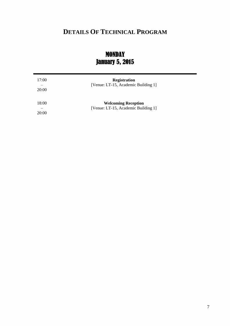
DETAILS OF TECHNICAL PROGRAM
MONDAY
January 5, 2015
17:00
–
20:00
Registration
[Venue: LT-15, Academic Building 1]
18:00
–
20:00
Welcoming Reception
[Venue: LT-15, Academic Building 1]

8
TUESDAY
January 6, 2015
07:45 Registration
[Venue: LT-15, Academic Building 1]
08:45 Welcome & Opening
[Venue: LT-17, Academic Building 1]
LU Jian
Vice President (Research & Technology)
City University of Hong Kong, Hong Kong
Session I – OLED Device and Materials I
Venue: LT-17, Academic Building 1 Chairman: CHE Chi-Ming (The University of Hong Kong, Hong Kong)
09:00 1.1 Nearly 100% electron-photon conversion by using novel strategy of
harvesting triplet excitons in organic light emitting devices
ADACHI Chihaya,
Kyushu University, Japan [Plenary]
09:45 1.2 Emitting Dipole Orientation of Phosphorescent Dyes in OLEDs
KIM Kwon-Hyeon, MOON Chang-Ki and KIM Jang Joo,
Seoul University, Korea [Invited]
Session II – Applications of Nano-Materials in Organic
Optoelectronics
Venue: LT-17, Academic Building 1 Chairman: ADACHI Chihaya (Kyushu University, Japan)
10:30 2.1 Adjusting the work function of inorganic semiconductors and
graphene with molecular donors and acceptors
KOCH Norbert,
Humboldt-Universität zu Berlin, Germany [Invited]
11:00 2.2 Preparation of high-quality single-crystal graphene and boron nitride
and their application in field-effect transistors
LIU Yunqi,
Institute of Chemistry, CAS, China [Invited]
11:30 2.3 Relaxed Anion-State in OLED Films Studied by High Sensitivity
Photoemission: Electron Injection Supported by Spontaneous
Orientation Polarization
KINJO Hiroumi, LIM Hyunsoo, SATO Hyungun Kim, T., NOGUCHI Y.,
NAKAYAMA Y., and ISHII Hisao,
Chiba University, Japan [Invited]
10:15 BREAK & POSTER VIEWING
12:15 LUNCH (City Top Restaurant, 9/F, Amenities Building)
12:00 GROUP PHOTO TAKING
9
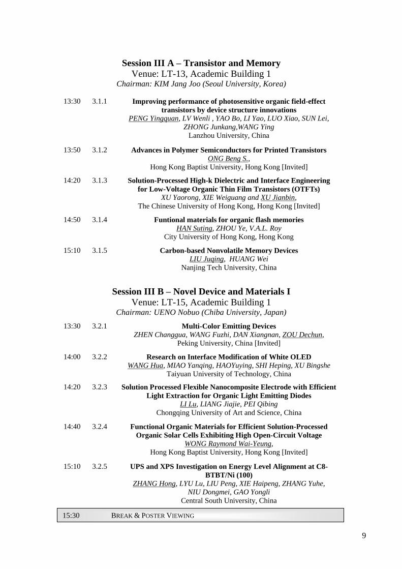
Session III A – Transistor and Memory
Venue: LT-13, Academic Building 1 Chairman: KIM Jang Joo (Seoul University, Korea)
13:30 3.1.1 Improving performance of photosensitive organic field-effect
transistors by device structure innovations
PENG Yingquan, LV Wenli , YAO Bo, LI Yao, LUO Xiao, SUN Lei,
ZHONG Junkang,WANG Ying
Lanzhou University, China
13:50 3.1.2 Advances in Polymer Semiconductors for Printed Transistors
ONG Beng S.,
Hong Kong Baptist University, Hong Kong [Invited]
14:20 3.1.3 Solution-Processed High-k Dielectric and Interface Engineering
for Low-Voltage Organic Thin Film Transistors (OTFTs)
XU Yaorong, XIE Weiguang and XU Jianbin,
The Chinese University of Hong Kong, Hong Kong [Invited]
14:50 3.1.4 Funtional materials for organic flash memories
HAN Suting, ZHOU Ye, V.A.L. Roy
City University of Hong Kong, Hong Kong
15:10 3.1.5 Carbon-based Nonvolatile Memory Devices
LIU Juqing, HUANG Wei
Nanjing Tech University, China
Session III B – Novel Device and Materials I
Venue: LT-15, Academic Building 1 Chairman: UENO Nobuo (Chiba University, Japan)
13:30 3.2.1 Multi-Color Emitting Devices
ZHEN Changgua, WANG Fuzhi, DAN Xiangnan, ZOU Dechun,
Peking University, China [Invited]
14:00 3.2.2 Research on Interface Modification of White OLED
WANG Hua, MIAO Yanqing, HAOYuying, SHI Heping, XU Bingshe
Taiyuan University of Technology, China
14:20 3.2.3 Solution Processed Flexible Nanocomposite Electrode with Efficient
Light Extraction for Organic Light Emitting Diodes
LI Lu, LIANG Jiajie, PEI Qibing
Chongqing University of Art and Science, China
14:40 3.2.4 Functional Organic Materials for Efficient Solution-Processed
Organic Solar Cells Exhibiting High Open-Circuit Voltage
WONG Raymond Wai-Yeung,
Hong Kong Baptist University, Hong Kong [Invited]
15:10 3.2.5 UPS and XPS Investigation on Energy Level Alignment at C8-
BTBT/Ni (100)
ZHANG Hong, LYU Lu, LIU Peng, XIE Haipeng, ZHANG Yuhe,
NIU Dongmei, GAO Yongli
Central South University, China
15:30 BREAK & POSTER VIEWING

10
Session IV A – OLED Device and Materials II
Venue: LT-13, Academic Building 1 Chairman: LIU Yunqi (Institute of Chemistry, CAS, China)
15:45 4.1.1 High efficiency white organic light-emitting diodes using thermally
activated delayed fluorescent emitters
CHO Yong Joo, KIM Bo Seong, YOOK Kyoung Soo and LEE Jun Yeob,
Dankook University, Korea [Invited]
16:15 4.1.2 Study of red fluorescent OLED utilizing delayed fluorescent
exciplex as the host
LI Wenlian, ZHAO Bo, SU Zisheng, CHU Bei
Changchun Institute of Optics, Fine Mechanics and Physics, CAS, China [Invited]
16:45 4.1.3 Development of Host and Dopant Materials for Phosphorescent
Organic Light-Emitting Diodes
LI Jiuyan, LI Wei, WANG Feng
Dalian university of technology, China
17:05 4.1.4 Novel Bipolar Host Materials for Phosphorescent and TADF OLEDs
LIU Di, WANG Miao, YAO Ruijuan
Dalian University of Technology, China
17:25 4.1.5 Solution-Processable Hosts Constructed by Carbazole/PO Substituted
Tetraphenylsilanes for Efficient Blue Electrophosphorescent Devices
LIU He, HU Dehua, LU Ping, MA Yuquang
Jilin University, Hong Kong
17:45 4.1.6 High efficiency OLED based on ultra-thin emission layer
HE Gufeng, LIU Jun, SHI Xindong
Shanghai Jiao Tong University, China
11
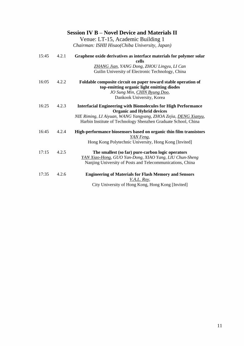
Session IV B – Novel Device and Materials II
Venue: LT-15, Academic Building 1 Chairman: ISHII Hisao(Chiba University, Japan)
15:45 4.2.1 Graphene oxide derivatives as interface materials for polymer solar
cells
ZHANG Jian, YANG Dong, ZHOU Lingyu, LI Can
Guilin University of Electronic Technology, China
16:05 4.2.2 Foldable composite circuit on paper toward stable operation of
top-emitting organic light emitting diodes
JO Sung Min, CHIN Byung Doo,
Dankook University, Korea
16:25 4.2.3 Interfacial Engineering with Biomolecules for High Performance
Organic and Hybrid devices
NIE Riming, LI Aiyuan, WANG Yangyang, ZHOA Zejia, DENG Xianyu,
Harbin Institute of Technology Shenzhen Graduate School, China
16:45 4.2.4 High-performance biosensors based on organic thin film transistors
YAN Feng,
Hong Kong Polytechnic University, Hong Kong [Invited]
17:15 4.2.5 The smallest (so far) pure-carbon logic operators
YAN Xiao-Hong, GUO Yan-Dong, XIAO Yang, LIU Chun-Sheng
Nanjing University of Posts and Telecommunications, China
17:35 4.2.6 Engineering of Materials for Flash Memory and Sensors
V.A.L. Roy,
City University of Hong Kong, Hong Kong [Invited]

12
WEDNESDAY
January 7, 2015
Session V – Perovskite and Organic Solar Cell I
Venue: LT-17, Academic Building 1 Chairman: YAM Vivian Wing Wah (The University of Hong Kong, Hong Kong)
09:00 5.1 Perovskite Solar Cell
PARK Nam-Gyu,
Sungkyunkwan University, Korea [Invited]
09:30 5.2 Nickel oxide p-type electrode interlayer in CH3NH3PbI3
perovskite/fullerene planar-heterojunction hybrid solar cells
JENG Jun-Yuan, CHEN Kuo-Cheng, CHIANG Tsung-Yu,
GUO Tzung-Fang, and CHEN Peter
National Cheng Kung University, Taiwan [Invited]
10:00 5.3 Electrode Buffer Layer Materials for High Performance Polymer
Solar Cells
LI Yongfang,
Institute of Chemistry, CAS, China [Invited]
Session VI – OLED and Organic Solar Cell
Venue: LT-17, Academic Building 1 Chairman: PARK Nam-Gyu (Sungkyunkwan University, Korea)
10:45
6.1 Unlocking Full Potential of Conducting Polymers for Highly Efficient
OLEDs and Solar Cells
WU Chung-Chih, HUANG Yi-Hsiang, LU Chun-Yang, LEE Wei-Kai,
TSAI Wei-Lung, JIAO Min
National Taiwan University, Taiwan [Invited]
11:15 6.2 Thermochromism Study of Low Band-Gap Photovoltaic Polymers
CHEN Chin-Ti,
Institute of Chemistry, Taiwan [Invited]
11:45 6.3 Functional Molecular Materials – From Design to Functions and
Applications
YAM Vivian Wing Wah,
The University of Hong Kong, Hong Kong [Invited]
10:30 BREAK & POSTER VIEWING
12:15 LUNCH (City Top Restaurant, 9/F, Amenities Building)
13
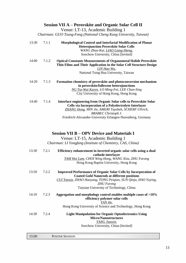
Session VII A – Perovskite and Organic Solar Cell II
Venue: LT-13, Academic Building 1 Chairman: GUO Tzung-Fang (National Cheng Kung University, Taiwan)
13:30 7.1.1 Morphological Control and Interfacial Modification of Planar
Heterojunction Perovskite Solar Cells
WANG Zhao-Kui, LIAO Liang-Sheng,
Soochow University, China [Invited]
14:00 7.1.2 Optical Constants Measurements of Organometal Halide Perovskite
Thin Films and Their Application in the Solar Cell Structure Design
LIN Hao-Wu,
National Tsing Hua University, Taiwan
14:20 7.1.3 Formation chemistry of perovskite and photoconversion mechanism
in perovskite/fullerene heterojunctions
NG Tsz-Wai Karen, LO Ming-Fai, LEE Chun-Sing
City University of Hong Kong, Hong Kong
14:40 7.1.4 Interface engineering from Organic Solar cells to Perovskite Solar
Cells via Incorporation of a Polyelectrolyte Interlayer
ZHANG Hong, MIN Jie, AMERI Tayebeh, SCHERF Ullrich,
BRABEC Christoph J.
Friedrich-Alexander-University Erlangen-Nuremberg, Germany
Session VII B – OPV Device and Materials I
Venue: LT-15, Academic Building 1 Chairman: LI Yongfang (Institute of Chemistry, CAS, China)
13:30 7.2.1 Efficiency enhancement in inverted organic solar cells using a dual
cathode interlayer
TAM Hoi Lam, CHOI Wing Hong, WANG Xizu, ZHU Furong
Hong Kong Baptist University, Hong Kong
13:50 7.2.2 Improved Performance of Organic Solar Cells by Incorporation of
Coated Gold Nanorods at different positions
CUI Yanxia, ZHAO Haoyang, TONG Peiqian, SUN Qinju, HAO Yuying,
ZHU Furong
Taiyuan University of Technology, China
14:10 7.2.3 Aggregation and morphology control enables multiple cases of >10%
efficiency polymer solar cells
YAN He,
Hong Kong University of Science and Technology, Hong Kong
14:30 7.2.4 Light Manipulation for Organic Optoelectronics Using
Micro/Nanostructures
TANG Jianxin,
Soochow University, China [Invited]
15:00 POSTER SESSION

14
Session VIII A – OPV Device and Materials II
Venue: LT-13, Academic Building 1 Chairman: WU Chung-Chih (National Taiwan University, Taiwan)
16:30 8.1.1 Effect of film drying condition on performance of polymer solar cells
for bis-PCBM/P3HT
MASARU Nagai, HUANG Wei, YOSHIDA Yuji
Nanjing Tech University, China
16:50 8.1.2 Efficiency enhancement in inverted organic solar cells using a dual
cathode interlayer
WU Bo, WU Zhenghui, LAM Tam Hoi, ZHU Furong, NG Tsz-Wai,
LEE Chun-Sing
Hong Kong Baptist University, Hong Kong
17:10 8.1.3 Printing Fabrication and Interface Materials for
Solution-Processed Organic Photovoltaics
YANG Junliang, XIONG Jian, HU Qiao, GAO Yongli
Central South University, China
17:30 8.1.4 Interface Engineering and Morphology Control for High
Performance Perovskite/Fullerene Planar Heterojunction Solar Cells
YIP Hin-Lap Angus, XUE Qifan, CHEN Sun, HU Zhicheng,
HUANG Fei, CAO Yong
South China University of Technology, China
17:50 8.1.5 Improved organic photovoltaics by surface plasmon effect
HAO Yuying, CUI Yanxia, ZHANG Ye, WANG Wenyan, TIAN Ximin,
HAO Yang, ZHU Furong
Taiyuan University of Technology, China [Invited]
18:20 DINNER (Shanghai Min, Tsim Sha Tsui)

15
Session VIII B – OPV Device and Materials III
Venue: LT-15, Academic Building 1 Chairman: CHEN Chin-Ti (Institute of Chemistry, Taiwan)
16:30 8.2.1 Contrary interfacial exciton dissociation at metal/organic interface in
regular and inverted organic solar cells
WU Bo, WU Zhenghui, YANG Qingyi, LIU Hanxiao, TAM Hoi Lam,
ZHU Furong,
Hong Kong Baptist University, Hong Kong [Invited]
17:00 8.2.2 Photovoltage Loss in Excitonic Solar cells
TSANG Sai Wing Stephen,
City University of Hong Kong, Hong Kong
17:20 8.2.3 High-efficiency all-polymer solar cells based
on a pair of crystalline low-bandgap polymers
MU Cheng, LIU Peng, MA Wei, JIANG Kui, ZHAO Jingbo, ZHANG Kai,
CHEN Zhihua, WEI Zhanhua, YI Ya, WANG Jiannong, YANG Shihe,
HUANG Fei, FACCHETTI Antonio, ADE Harald, YAN He
Hong Kong University of Science and Technology, Hong Kong
17:40 8.2.4 A Small-MoleculePhenanthroline Derivative as Cathode Interfacial
Material for Organic Photovoltaics
ZHU Xu-Hui,
South China University of Technology, China
18:20 DINNER (Shanghai Min, Tsim Sha Tsui)

16
THURSDAY
January 8, 2015
Session IX – OPV and OLED
Venue: LT-17, Academic Building 1 Chairman: CHEAH Kok-Wai (Hong Kong Baptist University, Hong Kong)
09:00 9.1 Efficiency and Reliability of Small Molecule Organic Photovoltaics
FORREST Stephen,
University of Michigan, USA [Plenary]
09:45 9.2 Structural details and measurements related to organic nanodevice
by STM
WAN Li-Jun,
Institute of Chemistry, CAS, China [Invited]
Session X – Organic Device and Interface
Venue: LT-17, Academic Building 1 Chairman: FORREST Stephen (University of Michigan, USA)
10:45 10.1 Interface effects in organic photovoltaics
BAO Qinye, SANDBERF Oskar, DAGNELUND Daniel, SANDÉN Simon,
GAO Feng, BRAUN Slawomir, AARNIO Harri, LIU Xianjie, CHEN
Weimin M., ÖSTERBACKA Ronald and FAHLMAN Mats,
Linköping University, Sweden [Invited]
11:15 10.2 Photocatalytic Reduction of Protons to Hydrogen
TUNG Chen-Ho, WU Li-Zhu, CHEN Bin, LI Zhi-Jun
Technical Institute of Physics and Chemistry, CAS, China [Invited]
11:45 10.3 Origin and control of gap states: A striking mobility improvement of
C60 OFET
YANG Jin-Peng, BUSSOLOTTI Fabio, HINDERHOFER Alexander,
KERA Satoshi, and UENO Nobuo,
Chiba University, Japan [Invited]
10:15 BREAK & POSTER VIEWING
12:15 LUNCH (City Top Restaurant, 9/F, Amenities Building)

17
Session XI – OLED Device and Materials III
Venue: LT-17, Academic Building 1 Chairman: WAN Li-Jun (Institute of Chemistry, CAS, China)
13:30 11.1 Transition Metal Phosphors and OLED Fabrications
CHI Yun,
National Tsing Hua University, Taiwan [Invited]
14:00 11.2 Universal Bipolar Host Materials And Exciplex For White OLEDs
WONG Ken-Tsung,
National Taiwan University, Taiwan [Invited]
14:30 11.3 New Schemes for Enhancing the Optical Management and Carrier
Transport Properties of Organic Optoelectronic Devices
CHOY C.H. Wallace
The University of Hong Kong, Hong Kong [Invited]
15:00 11.4 Reverse Intersystem Crossing from Upper Triplet Levels to Excited
Singlet: A “Hot excition” Path for OLEDs
MA Yuguang,
South China University of Technology, China [Invited]
Session XII – Novel Device and Materials III
Venue: LT-17, Academic Building 1 Chairman: V.A.L. Roy (City University of Hong Kong, Hong Kong)
15:45 12.1 Highly Efficient New Emitting Materials Based on Multi-Core
Chromophores for Blue Fluorescence OLEDs
PARK jongwook, LEE Hayoon, KIM Beomjin, KIM Seungho,
LEE Jaehyun, SHIN Hwangyu
Catholic University of Korea, Korea [Invited]
16:15 12.2 Aggregation-Induced Emission
TANG Benzhong,
Hong Kong University of Science and Technology, Hong Kong [Invited]
16:45 12.3 Pentacene-Based Organic Transistor Memory Devices with Charge-
Storage Floating Gate
TSENG Chia-Wei, HUANG Ding-Chi, TAO Yu-Tai,
Institute of Chemistry, Academia Sinica,, Taiwan [Invited]
----- End -----
15:00 BREAK & POSTER VIEWING
17:15 CLOSING REMARKS & BEST POSTER AWARD PRESENTATION
18
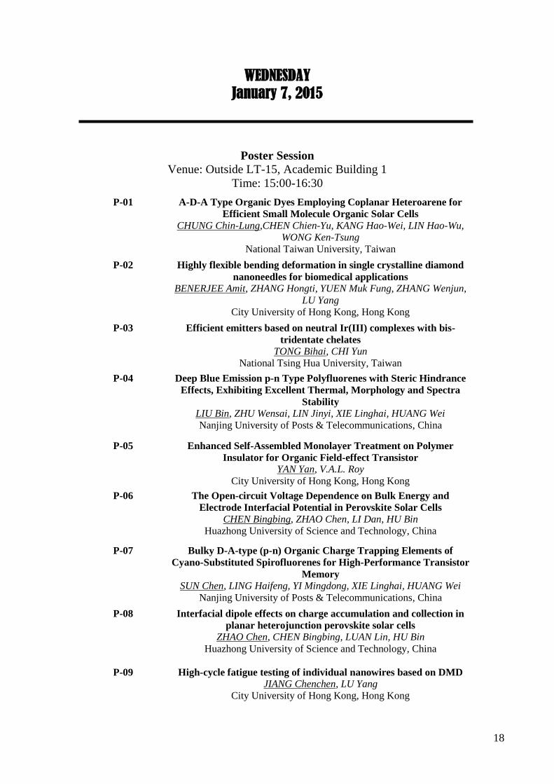
WEDNESDAY
January 7, 2015
Poster Session
Venue: Outside LT-15, Academic Building 1
Time: 15:00-16:30
P-01 A-D-A Type Organic Dyes Employing Coplanar Heteroarene for
Efficient Small Molecule Organic Solar Cells
CHUNG Chin-Lung,CHEN Chien-Yu, KANG Hao-Wei, LIN Hao-Wu,
WONG Ken-Tsung
National Taiwan University, Taiwan
P-02 Highly flexible bending deformation in single crystalline diamond
nanoneedles for biomedical applications
BENERJEE Amit, ZHANG Hongti, YUEN Muk Fung, ZHANG Wenjun,
LU Yang
City University of Hong Kong, Hong Kong
P-03 Efficient emitters based on neutral Ir(III) complexes with bis-
tridentate chelates
TONG Bihai, CHI Yun
National Tsing Hua University, Taiwan
P-04 Deep Blue Emission p-n Type Polyfluorenes with Steric Hindrance
Effects, Exhibiting Excellent Thermal, Morphology and Spectra
Stability
LIU Bin, ZHU Wensai, LIN Jinyi, XIE Linghai, HUANG Wei
Nanjing University of Posts & Telecommunications, China
P-05 Enhanced Self-Assembled Monolayer Treatment on Polymer
Insulator for Organic Field-effect Transistor
YAN Yan, V.A.L. Roy
City University of Hong Kong, Hong Kong
P-06 The Open-circuit Voltage Dependence on Bulk Energy and
Electrode Interfacial Potential in Perovskite Solar Cells
CHEN Bingbing, ZHAO Chen, LI Dan, HU Bin
Huazhong University of Science and Technology, China
P-07 Bulky D-A-type (p-n) Organic Charge Trapping Elements of
Cyano-Substituted Spirofluorenes for High-Performance Transistor
Memory
SUN Chen, LING Haifeng, YI Mingdong, XIE Linghai, HUANG Wei
Nanjing University of Posts & Telecommunications, China
P-08 Interfacial dipole effects on charge accumulation and collection in
planar heterojunction perovskite solar cells
ZHAO Chen, CHEN Bingbing, LUAN Lin, HU Bin
Huazhong University of Science and Technology, China
P-09 High-cycle fatigue testing of individual nanowires based on DMD
JIANG Chenchen, LU Yang
City University of Hong Kong, Hong Kong

19
P-10 Bipolar spin-filtering, rectifying and giant magnetoresistance effects
in zigzag silicene nanoribbons with asymmetric edge hydrogenation
ZHANG Dan, LONG Meng-Qiu, XU Hui, CHAN Kowksum
Central South University, China
P-11 Facile synthesis and optical characteristics of ZnSe and Mn:ZnSe
quantum dots
LIU Dong, LU Zhiyun, ZHANG jianquan, WU Lili, FENG Lianghuan
Sichuan University, China
P-12 Long operation lifetime and colour stable hybrid tandem white
organic light-emitting diodes for general lighting
WONG Fulung, FUNG Man Keung, LEE Chun Sing
City University of Hong Kong, Hong Kong
P-13 The influence of the thickness of electron transport layer on
the properties of organic light-emitting diodes
LIU Guohong, ZHOU Xiang
Sun Yat-Sen University, China
P-14 Smart sensors for printable electronics
ZHOU Ye, HAN Suting, V.A.L. Roy
City University of Hong Kong, Hong Kong
P-15 Nonvolatile Multilevel Organic Phototransistor Memory Using PVK
Derivative as Polymer Electrets
LING Haifeng, LI Lu, YI Mingdong, XIE Linghai, HUANG Wei
Nanjing University of Posts & Telecommunications, China
P-16 Capacitance measurements to investigate exciton behaviors in
organic photovoltaic materials
YU Haomiao, HOU Xiaoyuan
Fudan University, China
P-17 Synthesis and Electroluminescence Properties of Highly Efficient
Dual Core Chromophores with Side Groups for Blue Emission
LEE Hayoon, KIM Beomjin, KIM Seungho, KIM Joonghan, LEE
Jaehyun, SHIN Hwangyu, LEE Ji-Hoon, PARK Jongwook
The Catholic University of Korea, Korea
P-18 Study of Charge-transfer Complexes and the Application to
Organic Optoelectronics
MO Hin-Wai, LO Ming-Fai, NG Tsz-Wai, LEE Chun-Sing
City University of Hong Kong, Hong Kong
P-19 Alkoxyphenyl-Substituted Indacenodithiophenyl/Isomer Donor
Unit for
Efficient Bulk Heterojunction Solar Cells
HUANG Hongyan, LIU Shuli, ZHAO Baomin, HUANG Wei
Nanjing University of Posts and Telecommunications, China
P-20 Flexible and low-voltage organic field-effect transistors on
biodegradable cellulose paper
QIAN Chuan, SUN Jia, YANG Junliang, GAO Yongli
Central South University, China
P-21 Surface Mechanical Attrition Treatment (SMAT)-Facilitated
Fabrication of Porous Cu for Superior 3D Monolithic
Supercapacitor Electrodes
ZHANG Jie, LI Yangyang, LU Jian
City University of Hong Kong, Hong Kong
20
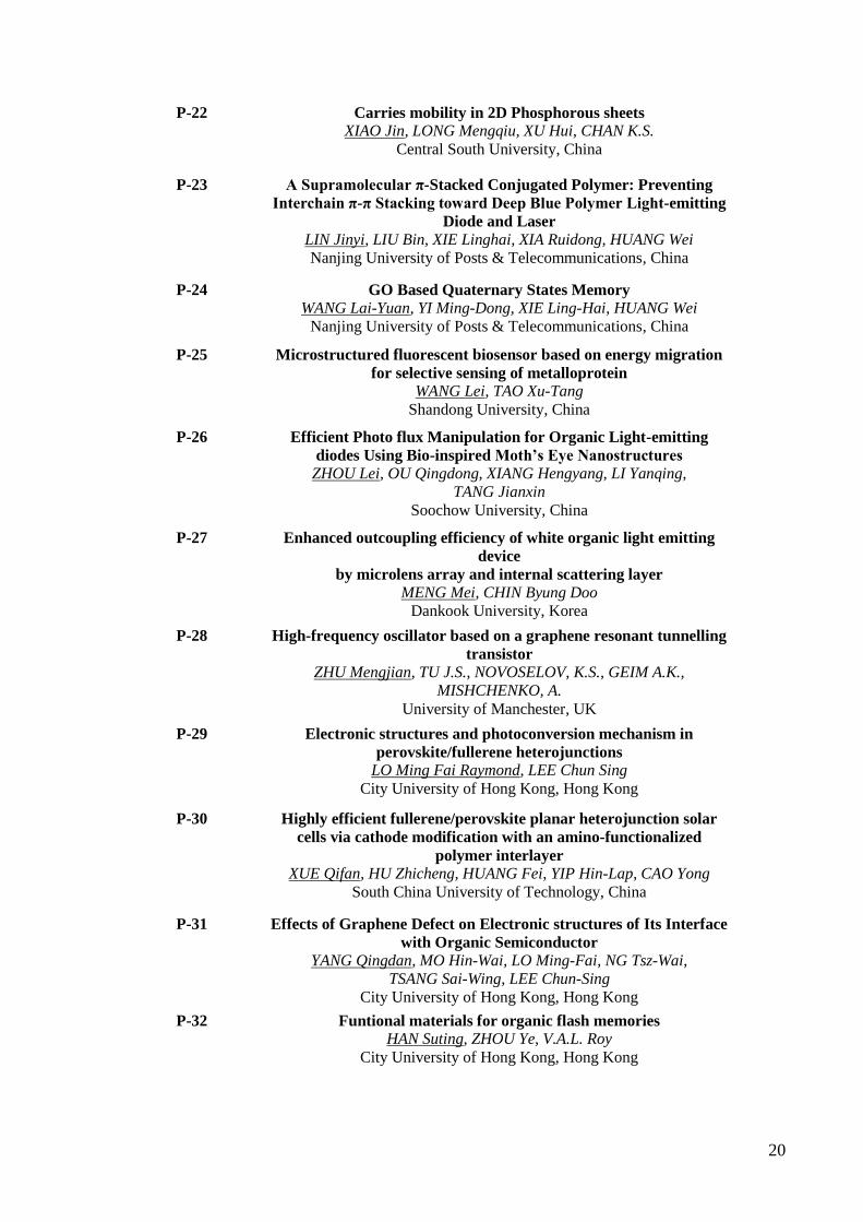
P-22 Carries mobility in 2D Phosphorous sheets
XIAO Jin, LONG Mengqiu, XU Hui, CHAN K.S.
Central South University, China
P-23 A Supramolecular π-Stacked Conjugated Polymer: Preventing
Interchain π-π Stacking toward Deep Blue Polymer Light-emitting
Diode and Laser
LIN Jinyi, LIU Bin, XIE Linghai, XIA Ruidong, HUANG Wei
Nanjing University of Posts & Telecommunications, China
P-24 GO Based Quaternary States Memory
WANG Lai-Yuan, YI Ming-Dong, XIE Ling-Hai, HUANG Wei
Nanjing University of Posts & Telecommunications, China
P-25 Microstructured fluorescent biosensor based on energy migration
for selective sensing of metalloprotein
WANG Lei, TAO Xu-Tang
Shandong University, China
P-26 Efficient Photo flux Manipulation for Organic Light-emitting
diodes Using Bio-inspired Moth’s Eye Nanostructures
ZHOU Lei, OU Qingdong, XIANG Hengyang, LI Yanqing,
TANG Jianxin
Soochow University, China
P-27 Enhanced outcoupling efficiency of white organic light emitting
device
by microlens array and internal scattering layer
MENG Mei, CHIN Byung Doo
Dankook University, Korea
P-28 High-frequency oscillator based on a graphene resonant tunnelling
transistor
ZHU Mengjian, TU J.S., NOVOSELOV, K.S., GEIM A.K.,
MISHCHENKO, A.
University of Manchester, UK
P-29 Electronic structures and photoconversion mechanism in
perovskite/fullerene heterojunctions
LO Ming Fai Raymond, LEE Chun Sing
City University of Hong Kong, Hong Kong
P-30 Highly efficient fullerene/perovskite planar heterojunction solar
cells via cathode modification with an amino-functionalized
polymer interlayer
XUE Qifan, HU Zhicheng, HUANG Fei, YIP Hin-Lap, CAO Yong
South China University of Technology, China
P-31 Effects of Graphene Defect on Electronic structures of Its Interface
with Organic Semiconductor
YANG Qingdan, MO Hin-Wai, LO Ming-Fai, NG Tsz-Wai,
TSANG Sai-Wing, LEE Chun-Sing
City University of Hong Kong, Hong Kong
P-32 Funtional materials for organic flash memories
HAN Suting, ZHOU Ye, V.A.L. Roy
City University of Hong Kong, Hong Kong
21
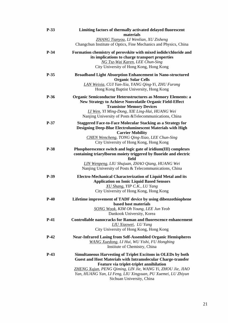
P-33 Limiting factors of thermally activated delayed fluorescent
materials
ZHANG Tianyou, LI Wenlian, XU Zisheng
Changchun Institute of Optics, Fine Mechanics and Physics, China
P-34 Formation chemistry of perovskite with mixed iodide/chloride and
its implications to charge transport properties
NG Tsz-Wai Karen, LEE Chun-Sing
City University of Hong Kong, Hong Kong
P-35 Broadband Light Absorption Enhancement in Nano-structured
Organic Solar Cells
LAN Weixia, CUI Yan-Xia, YANG Qing-Yi, ZHU Furong
Hong Kong Baptist University, Hong Kong
P-36 Organic Semiconductor Heterostructures as Memory Elements: a
New Strategy to Achieve Nonvolatile Organic Field-Effect
Transistor Memory Devices
LI Wen, YI Ming-Dong, XIE Ling-Hai, HUANG Wei
Nanjing University of Posts &Telecommunications, China
P-37 Staggered Face-to-Face Molecular Stacking as a Strategy for
Designing Deep-Blue Electroluminescent Materials with High
Carrier Mobility
CHEN Wencheng, TONG Qing-Xiao, LEE Chun-Sing
City University of Hong Kong, Hong Kong
P-38 Phosphorescence switch and logic gate of iridium(III) complexes
containing triarylboron moiety triggered by fluoride and electric
field
LIN Wenpeng, LIU Shujuan, ZHAO Qiang, HUANG Wei
Nanjing University of Posts & Telecommunications, China
P-39 Electro-Mechanical Characterization of Liquid Metal and its
Application on Ionic Liquid Based Sensors
XU Shang, YIP C.K., LU Yang
City University of Hong Kong, Hong Kong
P-40 Lifetime improvement of TADF device by using dibenzothiophene
based host materials
SONG Wook, KIM Oh Young, LEE Jun Yeob
Dankook University, Korea
P-41 Controllable nanocracks for Raman and fluorescence enhancement
LIU Xiaowei, LU Yang
City University of Hong Kong, Hong Kong
P-42 Near-Infrared Lasing from Self-Assembled Organic Hemispheres
WANG Xuedong, LI Hui, WU Yishi, FU Hongbing
Institute of Chemistry, China
P-43 Simultaneous Harvesting of Triplet Excitons in OLEDs by both
Guest and Host Materials with Intramolecular Charge-transfer
Feature via triplet-triplet annihilation
ZHENG Xujun, PENG Qiming, LIN Jie, WANG Yi, ZHOU Jie, JIAO
Yan, HUANG Yan, LI Feng, LIU Xingyuan, PU Xuemei, LU Zhiyun
Sichuan University, China
22
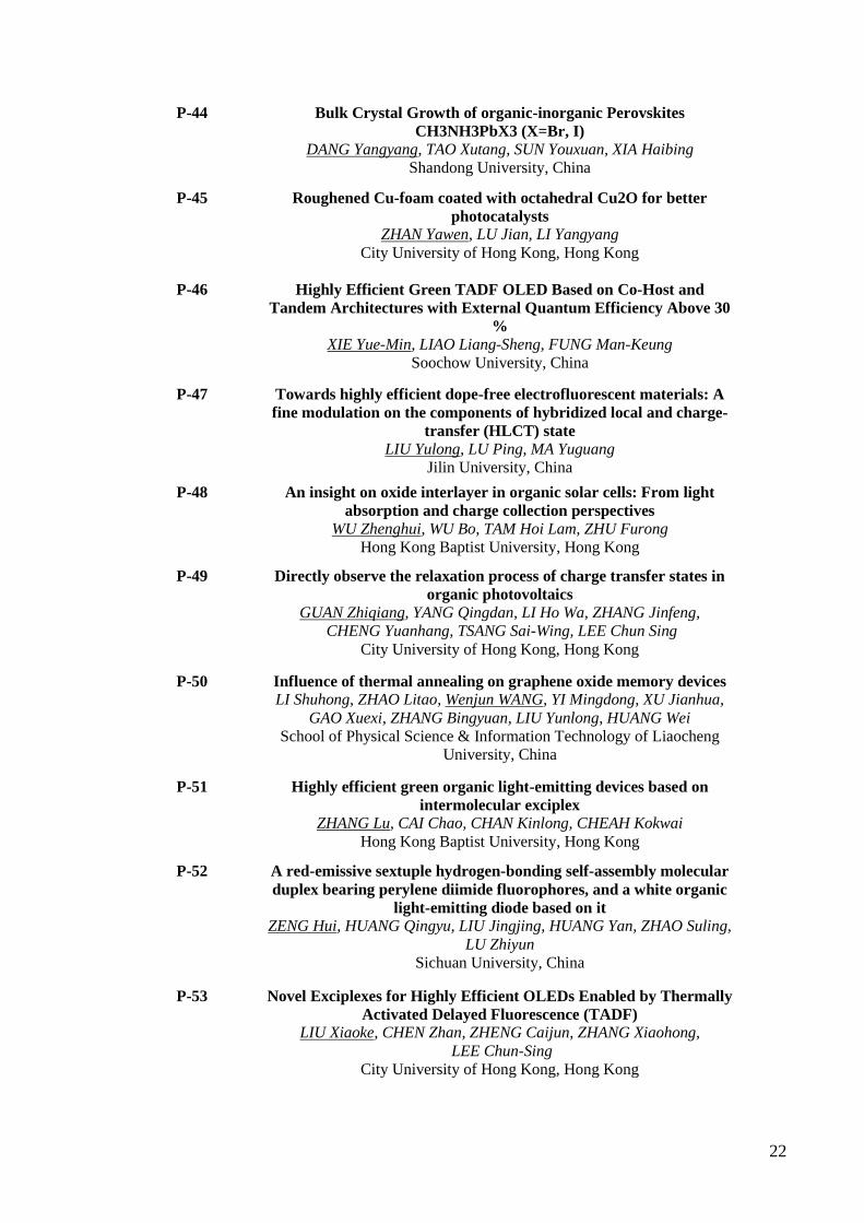
P-44 Bulk Crystal Growth of organic-inorganic Perovskites
CH3NH3PbX3 (X=Br, I)
DANG Yangyang, TAO Xutang, SUN Youxuan, XIA Haibing
Shandong University, China
P-45 Roughened Cu-foam coated with octahedral Cu2O for better
photocatalysts
ZHAN Yawen, LU Jian, LI Yangyang
City University of Hong Kong, Hong Kong
P-46 Highly Efficient Green TADF OLED Based on Co-Host and
Tandem Architectures with External Quantum Efficiency Above 30
%
XIE Yue-Min, LIAO Liang-Sheng, FUNG Man-Keung
Soochow University, China
P-47 Towards highly efficient dope-free electrofluorescent materials: A
fine modulation on the components of hybridized local and charge-
transfer (HLCT) state
LIU Yulong, LU Ping, MA Yuguang
Jilin University, China
P-48 An insight on oxide interlayer in organic solar cells: From light
absorption and charge collection perspectives
WU Zhenghui, WU Bo, TAM Hoi Lam, ZHU Furong
Hong Kong Baptist University, Hong Kong
P-49 Directly observe the relaxation process of charge transfer states in
organic photovoltaics
GUAN Zhiqiang, YANG Qingdan, LI Ho Wa, ZHANG Jinfeng,
CHENG Yuanhang, TSANG Sai-Wing, LEE Chun Sing
City University of Hong Kong, Hong Kong
P-50 Influence of thermal annealing on graphene oxide memory devices
LI Shuhong, ZHAO Litao, Wenjun WANG, YI Mingdong, XU Jianhua,
GAO Xuexi, ZHANG Bingyuan, LIU Yunlong, HUANG Wei
School of Physical Science & Information Technology of Liaocheng
University, China
P-51 Highly efficient green organic light-emitting devices based on
intermolecular exciplex
ZHANG Lu, CAI Chao, CHAN Kinlong, CHEAH Kokwai
Hong Kong Baptist University, Hong Kong
P-52 A red-emissive sextuple hydrogen-bonding self-assembly molecular
duplex bearing perylene diimide fluorophores, and a white organic
light-emitting diode based on it
ZENG Hui, HUANG Qingyu, LIU Jingjing, HUANG Yan, ZHAO Suling,
LU Zhiyun
Sichuan University, China
P-53 Novel Exciplexes for Highly Efficient OLEDs Enabled by Thermally
Activated Delayed Fluorescence (TADF)
LIU Xiaoke, CHEN Zhan, ZHENG Caijun, ZHANG Xiaohong,
LEE Chun-Sing
City University of Hong Kong, Hong Kong

23
P-54 Interface Engineering for high-performance, low-voltage n-channel
organic thin film transistors (OTFTs) based on C60
SU Yaorong, XIE Weiguang, XU Jianbin
The Chinese University of Hong Kong, Hong Kong
P-55 Enhanced Light Harvesting in Organic Solar Cells Featuring a Bio-
inspired Moth’s Eye Nanostructures
CHEN Jing-De, ZHOU Lei, CUI Chao-Hua, TANG Jian-Xin,
LI Yan-Qing, LI Yong-Fang
Soochow University, CHina
P-56 Highly efficiency electron transfer layer based on Ag, Al co-doped
ZnS in organic lighting emission diodes
HE Xiaoxiao, WANG Wenjun, LI Shuhong, LIU Yunlong, SHI Qiang,
WANG Qingru, ZHENG Wenquan
School of Physical Science & Information Technology of Liaocheng
University, China
P-57 The simulation study of fluid physical properties on drop formation
of drop-on-demand inkjet printing
ZHANG Lei, ZHU Yun-Long, CHENG Xiao-Ding, WANG Chi-Yuan
Shenyang Institute of Automation, China
P-58 Crystal-Domain Orientation and Boundary of Organic
Semiconductor Thin Film Investigated by in-situ Kelvin Probe
Force Microscopy
QIAN Chuan, SUN Jia, ZHANG Lei, HUNAG Han, YANG Junliang,
GAO Yongli
Central South University, China
P-59 Investigation on the roles of weight ratio between precursors in the
CVD growth of bilayered MoS2 crystals
HAO Song, YUAN Jingye, ZHANG Lei, HUANG Yingbao, WU Jun,
XIE Haipeng, GAO Yongli, YANG Bingchu, HUANG Han
Central South University, China
P-60 Electronic structures at the interface between Au and CH3NH3PbI3
LIU Xiaoliang, WANG Chenggong, LYU Lu, HUANG Jinsong,
GAO Yongli
Central South University, China
P-61 Fast and simplified fabrication of well-crystallized perovskite
methylammonium lead iodides films with a CVD method
CAO Huanqi, CHEN Xiaomin, YANG Liying, YIN Shougen
Tianjin University of Technology, China
P-62 Platinum-based Luminescent Metallomesogens: Synthesis,
Photophysical Properties and Application for OLEDs
SHI Junwei, WANG Yafei, YANG Chuncheng, ZHU Weiguo
Xiangtan University, China
P-63 Thickness Dependent Air-Exposure Induced Phase Transition of
CuPc Ultra-Thin Films to Well-Ordered One-Dimensional
Nanocrystals on Layered-Substrates
ZHANG Lei, YANG Yingguo, HUANG Han, LYU LU, ZHANG Hong,
CAO Ningtong, XIE Haipeng, GAO Xingyu, NIU Dongmei, GAO Yongli
Central South University, China

24
P-64 Elimination of the herringbone reconstruction of Au(111) surface
by self-assemblied HBB
TAN Zhiyu,ZHOU Zhenhong, TIAN Guo, GAO Yongli, HUANG Han
Central South University, China
P-65 Interfacial Energy level alignment at MoOx/CH3NH3PbI3 Interface
LIU Peng, LYU Lu, LIU Xiaoliang, NIU Dongmei, HUANG Jinsong,
GAO Yongli
Central South University, China
P-66 Effects of precursor ratios on electronic structure and surface
composition of perovskite films
XIE Haipeng, LYU Lu, LIU Xiaoliang, NIU Dongmei, HUANG Jinsong,
GAO Yongli
Central South University, China
P-67 The Study of Spectroscopic Properties of Colloidal Solutions of
Superparamagnetic Nanoparticles (Fe3O4/SiO2)
SMERDOV R.S.,BOCHAROVA T.V.
Saint-Petersburg State Polytechnical University, Russia
P-68 Highly Efficient Planar Heterojunction Perovskite Solar Cells
Fabricated by Solvent Engineering
WU Runsheng, XIONG Jian, CAO Chenghao,
ZHOU Conghua,
YANG Bingchu,
GAO Yongli,
YANG Junliang
Central South University, China
P-69 Boosting the Power Conversion Efficiency of Organic Solar Cells
Using Weakly Luminescent Gold(III) Corrole with Long-Lived
Exciton State LAI Shiu-Lun, WANG Lin, YANG Chen, CHAN Mei-Yee, GUAN
Xiangguo, KWOK Chi-Chung, CHE Chi-Ming
The University of Hong Kong, Hong Kong
25
Abstract of Talks
26
1.1
Nearly 100% electron-photon conversion by using novel strategy of harvesting
triplet excitons in organic light emitting devices
Chihaya Adachi1,2,a)
1 Center for Organic Photonics and Electronics Research (OPERA), Kyushu University, Japan,
2 JST, ERATO, Adachi Molecular Exciton Engineering Project, c/o Center for Organic Photonics
and Electronics Research (OPERA), Kyushu University, Japan
Keywords: OLED, TADF, Delayed fluorescence, upconversion, FRET
Organic light emitting diodes (OLEDs) have been anticipated to exhibit highly efficient, stable
emission aimed for displays and lighting applications. Here, we report the design rules for increasing
the electroluminescence efficiency based on thermally activated delayed fluorescence (TADF). We
show that a large delocalization of the highest occupied molecular orbital and lowest unoccupied
molecular orbital in these charge transfer compounds enhances the rate of radiative decay
considerably by inducing a large oscillator strength even when there is a small overlap between the
two wavefunctions. Further, through computational simulation, we identified intramolecular charge-
transfer (CT) molecules with small singlet-triplet CT state splitting but different energy relationships
between 3CT and locally-excited triplet (3LE) states. Systematic comparison of excited-state
dynamics revealed that CT molecules can emit efficient and short-lifetime (a few μs) TADF when
the emission peak energy is high enough and the 3LE state is higher than the 3CT state. The OLEDs
with TADF emitters offer an external quantum efficiency over 20% and reduced efficiency roll-off
characteristics at high luminance. Also, we mention the importance of molecular orientation for
enhancing light outcoupling efficiency. Some critical molecular design and processing condition will
be discussed.
Further, we report fluorescence-based OLEDs that realize external quantum efficiencies as
high as 20% for blue, green, yellow, and red emission, indicating that the exciton production
efficiency reached nearly 100%. The high performance was enabled by utilization of TADF
molecules as assistant dopants that permit efficient transfer of all electrically generated singlet and
triplet excitons from the assistant dopants to the fluorescent emitters. OLEDs employing this novel
exciton harvesting process provide freedom for the selection of emitters from a wide variety of
conventional fluorescent molecules.
References
[1] H. Uoyama, K. Goushi, K. Shizu, H. Nomura, C. Adachi, Nature, 492, 234 (2012)
[2] H. Nakanotani, T. Higuchi, T. Furukawa, K. Masui, K. Morimoto, M. Numata, H. Tanaka, Y.
Sagara, T. Yasuda, C. Adachi, Nat. Commun., 5, 4016 (2014)
27
1.2
Emitting Dipole Orientation of Phosphorescent Dyes in OLEDs (1 line spacing)
Kwon-Hyeon Kim, Chang-Ki Moon and Jang-Joo Kim)
Department of Materials Science and Engineering, Seoul National University, Seoul, Korea
(1 line spacing)
Keywords: oreientation, emitting dipoles, phosphorescent dyes, OLEDs.
(2 line spacing)
Molecular orientation in organic semiconductor is an important factor influencing electrical and
optical properties. In organic light emitting diodes (OLEDs), it has long been recognised that
orienting the transition dipole moment of an emitter along the horizontal direction (parallel to the
substrate) can enhance the outcoupling efficiency beyond that achieved under isotropic orientation,
as demonstrated in polymer-based and vacuum evaporated fluorescent molecule-based OLEDs.
Nonetheless, the orientation of the transition dipole moments of iridium complexes used as
phosphorescent emitters in efficient OLEDs is typically considered to be isotropic because they are
near-globular and small enough to have configurational diversity in their orientational states.
Therefore, it is believed that the theoretical EQE limit of phosphorescent OLEDs is 25~30%.
Recently, however, some heteroleptic iridium complexes (HICs) have been reported to have
transition dipole moments oriented preferentially along the horizontal direction. The outcoupling
efficiency of the emitted light from the horizontally oriented emit-ting dipoles in an OLED can reach
45% which is much higher than isotropically oriented transition dipoles. Unfortunately, the origin of
the preferred orientation of some phosphorescent dyes and factors influencing the orientation of the
transition dipole moments is not fully understood yet.
In this talk, we will firstly present the influence of the molecular structure of iridium complexes
and host materials on the orientation of the TDM in organic semiconductor layers in phosphorescent
dye doped organic layers. Secondly we will show through quantum chemical calculations that the
heteroleptic structure and the strong intermolecular interactions between HICs and their host
molecules lead to preferred dipole orientations in the HICs.
(1) Kwon-Hyeon Kim, et al., Nature Communications, 5, 4769 (2014)
(2) Kwon-Hyeon Kim, et al., Advanced Materials, 26, 3844 (2014)
(3) Kwon-Hyeon Kim, et al., submitted (2014)
(4) Chang-Ki Moon, et al., submitted (2014)

28
2.1
Adjusting the work function of inorganic semiconductors and graphene with
molecular donors and acceptors
Norbert Koch1,2a)
1Humboldt-Universität zu Berlin, Institut f. Physik, Newtonstr. 15, 12489 Berlin, Germany;
2Helmholtz-Zentrum Berlin f. Materialien und Energie GmbH, Renewable Energies, 12489 Berlin,
Germany
Keywords: semiconductors; graphene; interface electronic structure; work function.
Hybrid heterostructures of inorganic and organic semiconductors offer new possibilities for
obtaining enhanced functionality by combining the advantageous properties of the individual
components, e.g., towards efficient interfacial energy and charge transfer. To optimize the energy
levels at a given hybrid heterojunction one must have means to move the frontier energy levels
without compromising the targeted function. It will be shown how this can be achieved with either
dipolar self-assembled monolayers or strong molecular donors and acceptors as interlayers. The
underlying mechanism is based on modifying the inorganic semiconductor surface work function by
the interlayer, which leads to concomitant energy shifts of the organic semiconductor deposited on
top. However, the details of the charge density rearrangement due to interlayers, which results in a
changed work function, depend strongly on the doping level of the inorganic component.
A similar strategy, i.e., the use of strong molecular donors and acceptors, can be followed to
modify the work function of graphene, e.g., in order to optimize its use as electrode material for
charge injection in devices. The nature of charge transfer between molecules and graphene is very
different from that of inorganic semiconductors. Moreover, the material that serves as solid support
for a graphene layer (e.g., glass versus metal) strongly impacts the charge density rearrangement and
the electronic structure of graphene itself. This is demonstrated through a combined experimental
and theoretical approach.

29
2.2
Preparation of high-quality single-crystal graphene and boron nitride
and their application in field-effect transistors
Yunqi Liua)
Institute of Chemistry, Chinese Academy of Sciences, Beijing 100190, China
Keywords: preparation, graphene, boron nitride, field-effect transistor
Chemical vapor deposition (CVD) is widely used in the synthesis of graphene. In this method,
the graphene samples grown on metals need to be transferred onto insulating materials for use in
electronic devices, which results in loss of material, and furthermore it is difficult to avoid
corrugation, contamination, and breakage of the graphene samples. The direct metal-catalyst-free
growth of graphene on insulating substrates is thus important to the development of graphene nano-
electronics.[1,2]
Recently, we demonstrated that regular micrometer-size high-quality single domain graphene
can be directly grown on various dielectric substrates via a small-carbon-flow near-equilibrium CVD
process.[3]
The near-equilibrium CVD method allows C adatoms to reach the optional positions at the
edge of graphene sheets with minimum energy to form stable crystalline phases with regular
hexagonal and dodecagonal patterns. The maximum size of the graphene grains is about 11 μm,
which is a factor of ∼30 times larger than those previously reported on boron nitride (BN) substrates.
The graphene grains show high crystalline quality with clean, wrinkle-free and breakage-free
morphology, and a carrier mobility of greater than 5000 cm2 V
−1 s
−1.
We also report for the first time that by using a system of h-BN growth on Cu surface under
low-pressure CVD conditions,[4]
the nucleation density of h-BN can be significantly modulated in a
large range, resulting in an effective control of h-BN grain sizes. These h-BN grains are single-
layered, single crystals with a triangular shape, and the size can reach up to ca. 20 μm, 4–5 times
larger than that in previously achieved results. We further discovered that h-BN grains can be
directly visualized by optical microscopy by oxidizing Cu surface in air. Finally, we demonstrated
that the oxidation of h-BN film at high temperatures in air can effectively clean monolayer h-BN
film interface, leading to reliable and much enhanced graphene mobility.
1. Jianyi Chen, Yugeng Wen, Yunlong Guo, Bin Wu, Liping Huang, Yunzhou Xue, Dechao Geng,
Dong Wang, Gui Yu, and Yunqi Liu, J. Am. Chem. Soc., 2011, 133(44), 1754817551.
2. Jianyi Chen, Yunlong Guo, Yugeng Wen, Liping Huang, Yunzhou Xue, Dechao Geng, Bin Wu,
Birong Luo, Gui Yu, Yunqi Liu, Adv. Mater., 2013, 25(7), 992–997.
3. Jianyi Chen, Yunlong Guo, Lili Jiang, Zhiping Xu, Liping Huang, Yunzhou Xue, Dechao Geng,
Bin Wu, Wenping Hu, Gui Yu, and Yunqi Liu, Adv. Mater., 2014, 26(9), 13481353.
4. Lifeng Wang, Bin Wu, Jisi Chen, Hongtao Liu, Pingan Hu, and Yunqi Liu, Adv. Mater., 2014,
26(10), 15591564.
a) Presenting author’s Email: [email protected]

30
2.3
Relaxed Anion-State in OLED Films Studied by High Sensitivity Photoemission:
Electron Injection Supported by Spontaneous Orientation Polarization
Hiroumi Kinjo1, Hyunsoo Lim
1, Hyungun Kim
1, T. Sato
1, Y. Noguchi
2, Y. Nakayama
1, and Hisao
Ishii1,3, a),b)
1Graduate School of Advanced Integration Science, Chiba University,
2School of Science and Technology,
Meiji University, 3 Center for Frontier Science, Chiba University,
1-33 Yayoi-cho, Inage-ku, Chiba-shi 263-8522 Japan Japan
Keywords: High-Sensitivity Photoelectron Spectroscopy, Photoelectron Yield Spectroscopy,
Negative Ion Photoelectron Spectroscopy, Alq3, Orientation Polarization
Organic EL materials often show spontaneous orientation polarization in evaporated films with giant
surface potential (GSP)[1]. This polarization induces positive and negative fixed charges on both ends of the
polarized layer, leading to interface charges at organic/organic and organic/electrode interfaces in organic
light-emitting devices. These interface charges often attract and repel carriers, and significantly affects the
device performance. In this study, by focusing on Alq3-based OLED, the impact of orientation polarization
was investigated from the viewpoints of carrier behavior and electronic structures.
Displacement current measurement (DCM) was performed for ITO/-NPD/Alq3/Al and ITO/-
NPD/Al(7-prq)3/Ca devices. Al(7-prq)3 is a derivative of Alq3; the position 7 is replaced by propyl group.
These two molecules show opposite polarity of polarization; the cathode side of Alq3 has positive interface
charge, but negative for Al(7-prq)3. DCM results suggested that positive interface charge near the cathode can
support electron injection, while negative charge increases the resistance [2]. This trend was also supported by
photoemission experiments as below.
By using high-sensitivity photoelectron spectroscopy (HS-PES) and photoelectron yield spectroscopy
(PYS), we have found unusual photoemission from films of Alq3 with GSP. Even if the photon energy is
smaller than their ionization energy, photoelectrons are clearly observed. As shown in Fig.1, the ionization
energy of Alq3 is about 5.6eV, but we observed that PYS spectrum has a threshold around 2.8eV, and HS-PES
measurement indicates the existence of some state 2eV above the Fermi level of the substrate. On the other
hand, for Al(7-prq)3, the unusual photoemission was not observed. Due to the opposite polarity of
polarization, anion and cation are expected to be accumulated
at the surfaces of Alq3 and Al(7-prq)3, respectively. From
these results, we suggest that the observed unusual
photoemission is ascribed to photoemission from negative
carriers that are captured only for the surface of Alq3 film.
Usually electron affinity has been observed by inverse
photoemission spectroscopy (IPES), in which radiation
damage and poor energy resolution are serious problems. Our
finding can be extended to develop as a method to determine
electron affinity of various organic EL materials with high
resolution and less damage. The electron affinity obtained in
this work seems larger than that reported by IPES, suggesting
the positive interface charge near the cathode effectively
stabilizes the anion states, leading to the reduction of electron
injection barrier. Therefore, the control of orientation
polarization and GSP of organic semiconductors is essential to
improve the performance of OLEDs.
References
(1) Y. Noguchi, Y. Miyazaki, Y. Tanaka, N. Sato, Y. Nakayama, T. D. Schmidt, W. Bruetting, and H. Ishii, J. of Appl.
Phys. 2012, 111, 114508.
(2) Y. Noguchi, H. Lim, T. Isoshima, E. Ito, M. Hara, W. W. Chin, J. W. Han, H. Kinjo, Y. Ozawa, Y. Nakayama, and H.
Ishii, Appl. Phys. Lett. 2013, 102, 203306.
a) , b) [email protected]
Fig.1 PYS of Alq3 and Al(7-Prq)3
films

31
3.1.1
Improving performance of photosensitive organic field-effect transistors by
device structure innovations
Yingquan Peng1,a)
, Wenli Lv1, Bo Yao
1,2, Yao Li
1, Xiao Luo
1, Lei Sun
1,Junkang Zhong
1,Ying
Wang1
1Institute of Microelectronics, School of Physical Science and Technology, Lanzhou University,
Lanzhou
730000, China, 2Department of Physics, Shaoxing University, Shaoxing 312000, China
Keywords: structure innovation; photosensitive; organic field-effect transistor; photoresponsivity.
Structure innovation is an important way to improve device performances. We demonstrate that
by utilizing buffer layer under source / drain electrodes or hybrid planar-bulk heterojunction the
performance of photosensitive organic field-effect transistors
(photOFETs) could be significantly improved. We fabricated
characterized top-contact pentacene photOFETs with C60
buffer layer under Au source/drain (S/D) electrodes (shown
in Fig. 1(a)). It showed an improvement of 125% for
mobility, and 600% for photoresponsivity at zero gate
voltage compared with that of the device without buffer
layer, which is already higher than the most recent reports on
the photoresponsivities of pentacene photOFETs [1, 2].
We fabricated
a high performance
photOFET operating in NIR region with a
structure of hybrid planar-bulk heterojunction (HPBHJ), as
shown in Fig. 2(a), where CuPc, PTCDA and PbPc, denote
copper phthalocyanine, 3,4,9,10-
perylenetetracarboxylic dianhydride
and lead phthalocyanine, respectively. It is
concluded that the photOFET with HPBHJ structure
showed superior performance compared to that with
other structures, and for NIR light of wavelength 808
nm, the photOFET with HPBHJ structure exhibited a large
photoresponsivity of 322 mA/W, a high external quantum
efficiency of around 50%, and a maximal
photosensitivity of 9.4×10².
[1]A. El Amrani, et al., Synthetic Metals, 161, 2566-2569 (2012).
[2]Y.-Y. Noh and D.-Y. Kim, Solid-State Electronics, 51, 1052-1055 (2007).
a) Presenting and corresponding author: [email protected]
FIG. 1. Structure of pentacene OPTs with
C60 electrode buffer layer
FIG. 1.(a) structure of hybrid planar-bulk
heterojunction; (b) Measured dependence
of drain current in the dark and
photocurrent on the thickness of
PbPc:PTCDA layer for HPBHJ devices
32
3.1.2
Advances in Polymer Semiconductors for Printed Transistors
Beng S. Ong
Research Centre of Excellence for Organic Electronics, Institue of Creativity and
Department of Chemistry, Hong Kong Baptist University
Kowloon Tong, Kowloon, Hong Kong
Printed electronics offers excellent opportunities for creating novel low-cost, large-area, lightweight
and flexible electronics. To realize this technology vision, manufacture of semiconductor devices by
high-throughput roll-to-roll printing, instead of traditional batch-wise photolithographic processes,
would be paramount. Printed electronics is innovative, potentially low-cost and eco-friendlier in
manufacturing, and enables inspiring device architectural design. Foremost among critical enablers
to propel this paradigm shift in manufacturing is a stable, solution-processed semiconductor for
fabricating functionally capable transistors. This presentation discusses the challenges and advances
in semiconductor development for printed transistors over the last decade and the outlook for this
emerging technology moving forward. Special emphasis will be devoted to recent advances in
ambient stable, solution-processed polymer semiconductors with high field-effect mobility, together
with excellent device shelf-life and operational stability characteristics.

33
3.1.3
Solution-Processed High-k Dielectric and Interface Engineering
for Low-Voltage Organic Thin Film Transistors (OTFTs)
Yaorong Su1, Weiguang Xie
2, Jianbin Xu
1a,b
1Department of Electronic Engineering and Materials Science and Technology Research Centre, The
Chinese University of Hong Kong, Shatin, Hong Kong SAR, China. 2Siyuan Laboratory, Department of Physics, Jinan University, Guangzhou, Guangdong, 510632, P.
R. China.
Keywords: high-k, solution processed, low voltage, OTFTs, interface engineering, flexible
Albeit huge progress has been made in improving the performance of organic thin film transistors
(OTFTs), the high operation voltage resulting from the low gate dielectric of traditional SiO2 remains
a severe limitation that impedes OTFTs’ development for practical applications. In this aspect, to
develop new high-k gate dielectrics at low cost is of great scientific and technological importance in
both academia and industry. Here, we report on a facile solution-based technique to fabricate high-k
metal oxide dielectric system (ATO) at low-temperature, which can be used effectively to realize
low-voltage operation of OTFTs. On the other hand, it is well known that the properties of the
dielectric/active channel and electrode/active channel interfaces are critical in controlling the
electrical properties of OTFTs. By optimizing the above two interfaces with octadecylphosphonic
acid (ODPA) self-assembled monolayer (SAM) and properly modifying low-cost Cu, improved
device performance is unequivocally attained among our low-voltage OTFTs. Moreover, organic
electronic devices on flexible substrates have attracted much attention due to their low-cost, roll-to-
roll capability, large-area processability, and so on. With the preceding techniques mentioned, good
electrical characteristics of OTFTs are achieved on flexible substrates. Our work demonstrates an
effective way to realize low-voltage, high-performance OTFTs at low-cost.
a),b)
e-mail: [email protected]
34
3.1.4
Funtional materials for organic flash memories
Su-Ting Han 1
, Ye Zhou 1, V. A. L. Roy
1
1Center of Super-Diamond and Advanced Films and Department of Physics and Materials Science,
City University of Hong Kong, Hong Kong, China
Email: [email protected]
Keywords: printed electronics, flash memory, floating gate, organic semiconductor, transistors
The next-generation electronic systems are expected to be light, flexible and portable for applications
in large area displays, integrated circuits (ICs), organic light emitting diodes (OLEDs), radio
frequency identification (RFID) tags, solar cells and so on. Memory is an essential part of advanced
electronic systems for data processing, storage and communication. Among many types of memories
such as ferroelectric, electret, resistive and floating gate, nano-floating gate flash memory devices
have gained a great deal of attention due to the simple device structure, non-destructive read-out and
controlled trap capacity. In this presentation, we will demonstrate recent works based on solution
processable or printable materials for organic flash memories.
35
3.1.5
Carbon-based Nonvolatile Memory Devices
Juqing Liu1,a,b)
, Wei Huang1
1F Key Laboratory of Flexible Electronics (KLOFE) & Institute of Advanced Materials (IAM),
Jiangsu National Synergistic Innovation Center for Advanced Materials (SICAM), Nanjing Tech
University (NanjingTech), 30 South Puzhu Road, Nanjing 211816, P.R. China
Keywords: Carbon materials, Graphene, Carbon Nanotube, Conducting films, Memory devices.
Low-dimensional carbon materials, such as graphene, carbon nanotubes (CNTs), fullerene, and
their derivatives, have attracted great attention in future electronics due to their unique electrical
properties. Herein, a series of memory electronic devices based on low-dimensional carbon
materials, mainly including all-reduced graphene oxide (rGO) memory and all-carbon fiber-based
memory [1,2], will being demonstrated. In the all-rGO memory device [1], both of top and bottom
electrodes are made of highly reduced GO (hrGO) films by high-temperature annealing of GO film,
and the active material is made of lightly reduced GO (lrGO) by low-temperature annealing of GO
film. The diode exhibits a nonvolatile WORM memory effect. In the all-carbon fiber memory,
aligned multi-walled carbon nanotube (MWCNT) fibers as conducting electrodes are coated by a
thin layer of GO as active layer. By simply cross-stacking two MWCNT@GO fibers, the fabricated
memory cell also shows WORM effect. The novel structure of MWCNT@GO fibers and facile
device fabrication process enable these memory cells promising for future smart e-textile
applications. In particular, our all-rGO component and full-solution process enable a low-cost,
environment-friendly, and mass-production of devices. Furthermore, highly conductive rGO films as
electrodes were introduced in flexible polymer memory diodes, e. g., bulk heterojunction polymer
memories and MoS2-based polymer memories using rGO electrodes exhibit WORM and Flash
memory effect, respectively [3,4]. Our study paves a way of employing low-dimensional carbon
materials as both electrical bistable materials and conductive materials for future data storage.
[1] Juqing Liu, Zongyou Yin, Xiehong Cao, et al., Adv. Mater., 25, 233-238 (2013)
[2] Gengzhi Sun, Juqing Liu, Lianxi Zheng, et al., Angew. Chem. Int. Ed., 52, 13351 (2013)
[3] Juqing Liu, Zhiyuan Zeng, Xiehong Cao, et al., Small 8, 3517 (2012)
[4] Juqing Liu, Zongyou Yin, Xiehong, et al., ACS Nano 4, 3987 (2010)
a) Presenting author’s Email: [email protected]
b) Corresponding author’s Email: [email protected]

36
3.2.1
Multi-Color Emitting Devices
Changgua Zhen,Fuzhi Wang, Xiangnan Dan, Dechun ZOU*
Beijing National Laboratory for Molecular Sciences, Key Laboratory of Polymer Chemistry and
Physics of Ministry of Education, College of Chemistry and Molecular Engineering, Peking
University, Beijing 100871.
Keywords: Electroluminescence, Electrochemiluminescence, Emitting device, Multi-color
The color of an emitting device is basically determined by the
emitting centers. In an OLED, the emitting centers are the emissive
molecules which exist in the carrier recombination zone and have the
narrowest band gap (Eg). Generally, once the emitting device was
fabricated, the carrier recombination zone was fixed, so we can get
only one color from one emitting device. If different color is needed,
the emissive molecules must be changed; this can be done by
fabricating a device with different emissive molecules. For example,
in a traditional RGB displays, one display pixel composes of multiple
emitting points, each of which emits one basic color. But this makes
the panel structure and the fabricating process be very complicated. In
this talk, we introduce a new type of multi-color emitting devices, in which different colors can be
emitted from the same device point.
We found that by a proper combination of electroluminescent layers and solid-state
electrochemiluminescent layers and electrodes, the injection and transportation of carriers can be
dynamically controlled, and thus the carrier recombination zone is controllable. Fig. 1 is a typical
two-color emitting device structure and Fig. 2 shows the emitted spectrum under different bias. By
changing the polarity or the magnitude of driving bias, the carrier recombination zone can be
switched to different layer in the device; we can also change the emission proportion between
different layers as shown above.
References
1. C. D. Müller, A. Falcou, et al., Nature 2003, 421, 829
2. C. L. Ho, L. C. Chi, et al., J. Mater. Chem., 2012, 22, 215
3. M. C. Gather, N. M. Kronenberg, K. Meerholz, Adv. Mater. 2010, 22, 4634
4. C. G. Zhen, Y. T. Chuai and D. C. Zou, Appl. Phys. Lett., 2005, 87, 093508
5. F. Z. Wang, D.C. Zou, et al., Appl.Phys.Lett., 2006, 89, 183519
Dechun ZOU*:E-mail: [email protected]
Figure 1. A typical two-color
emitting device structure
Figure 2. The emission spectra
under different bias Magnitude

37
3.2.2
Research on Interface Modification of White OLED
Wang Hua1, 2, a), b)
, Miao Yanqing1, 2
, Hao Yuying1, 3
, Shi Heping4, Xu Bingshe
1, 2
1 Key Laboratory of Interface Science and Engineering in Advanced Materials, Taiyuan University
of Technology, Ministry of Education, Taiyuan, 030024, China. 2 Research Center of Advanced
Materials Science and Technology, Taiyuan University of Technology, Taiyuan, 030024, China. 3
College of Physics and Optoelectronics, Taiyuan University of Technology, Taiyuan, 030024,
China.4School of Chemistry and Chemical Engineering, Shanxi University, Taiyuan 030006, China
Keywords: White, OLED, Interface
White OLED has acquired great attention due to unique properties, e.g. thin, light, flexible, energy
saving, which had been utilized as backlight of LCD display and indoor illumination. But, the device
performance of white OLEDs is rather poorer relative to LED, especially in device lifetime and color
stability, which hold back utilization progress of white OLED. In our early work [1-5]
, it has been
identified that the existence of plenty of interface in white OLED induce in degradation of device
performance. The interface is usually unstable in chemical and physical properties, owing to
different material structure or molecular structure in both sides of interface. Hence, it is demonstrated
by our group that optimization and modification of interface structure can improve device
performance. In our work, white-light phosphorescence polymers with hyperbranced structure were
designed and synthesized, which can be utilized in white OLED with single emission layer for
decreasing multilayers interface; homogeneous interface of AlQ3 were modified by SiO2 coating for
avoiding invasion of moisture and oxygen, resulting in prolonging device lifetime; ultra-high color
stable three color fluorescent-phosphorescent hybrid white OLED was designed and fabricated by
lowering heterogeneous interface number in emitting layers, which exhibit ideal CCTs around 3810
K and stable CIE coordinates of (0.40, 0.41) with high CRI of 85-86 upon variation in brightness
from 100 to 5000 cd/m2 (as shown in the ). In one word, it is suggested that interface research is very
important for enhancing performance of white OLED.
Fig. 1 The EL spectra of the hybrid WOLED at different luminance
Reference
[1] H. Wang, Y. Xu, T. Tsuboi, et al. Organic Electronics. 2013, 14,827.
[2] H.H. Liu, F. Yan, H. Wang, et al. Appl. Phys. Lett. 2013, 102, 013304.
[3] Y.Y. Hao, W.X. Meng, H.X. Xu, et al. Organic Electronics. 2011, 12, 136.
[4] H.P. Shi, D.H. Xin, X.Q. Dong, et al. Journal of Materials Chemistry C. 2014, 2, 2160.
[5] H. Wang, X.G. Du, W.M. Su, et al. AIP Advances. 2014, 4(2), 027103.
a) Presenting author’s Email: [email protected]
b) Corresponding author’s Email: [email protected]

38
3.2.3
Solution Processed Flexible Nanocomposite Electrode with Efficient Light
Extraction for Organic Light Emitting Diodes (1 line spacing)
Lu Li1,2a) b)
, Jiajie Liang2, Qibing Pei
2,b)
1New Materials Research Institute, Chongqing University of Art and Science, Chongqing, China
402160, 2 Department of Materials Sciences and Engineering, California NanoSystems Institute, Henry
Samuli School of Engineering and Applied Science, University of California, Los Angeles,
California 90095
(1 line spacing)
Keywords: Flexible organic light-emitting diodes, solution process, nanocomposite, light extraction
(2 line spacing)
The application of organic LEDs (OLEDs) to reduce the energy consumption for lighting and
display has attracted tremendous interest in academic research and technology development. The
nearly quantum yield of electron-to-photon conversion efficiency in OLEDs has been largely un-
utilized as the external quantum efficiency are limited to 20% due to light trapping in the sandwich
device structure. Flexible and solution-processed OLEDs have even worse performance. Here we
report a solution-processed flexible nanocomposite electrode with efficient light extraction. The
nanocomposite comprises a bilayer stack of carbon nanotubes and silver nanowires inlaid in the
surface of a nanoparticle-polymer composite membrane. The nanocomposite is designed to exhibit
high surface conductivity, low surface roughness, and high light extraction efficiency. Flexible
polymer OLEDs based on the nanocomposite substrate exhibit external quantum efficiency as high
as 38.9%, which is significantly higher than the reported highest efficiency for any OLEDs without
the use of an external light collection structure, including small molecule OLEDs comprising
multiple layers of vacuum-deposited organic compounds to increase the internal quantum efficiency
to unity. The viewing angle of the PLEDs is also improved such that the emission color from the 90
degree angle is identical to the normal angle.
a) Presenting author’s Email [email protected]
b) Corresponding author’s Email [email protected] and [email protected]

39
3.2.4
Functional Organic Materials for Efficient Solution-Processed Organic Solar
Cells Exhibiting High Open-Circuit Voltage
Wai-Yeung Wong a)
Institute of Molecular Functional Materials and Department of Chemistry, Hong Kong Baptist
University, Waterloo Road, Kowloon Tong, Hong Kong.
Keywords: Organic photovoltaics, Open-circuit voltage, 2D-conjugated molecules, Donor-acceptor
molecules
Organic solar cells (OSCs) have drawn great interest over the past decade since they possess unique
advantages such as low cost, light-weight and good mechanical flexibility. To date, the power
conversion efficiency (PCE) of polymer-based OSCs has exceeded 10%. Meanwhile, solution-
processed small molecule bulk heterojunction OSCs are emerging as a competitive alternative to
their polymer counterparts. Compared to polymers, small molecular semiconductors possess the
intrinsic advantages of well-defined structure, good synthetic reproducibility, alleviated batch-to-
batch variation and easier band structure control. Much effort is still required to develop new
materials and understand the relationship between chemical structures of the materials and device
performance factors such as open-circuit voltage (Voc), short-circuit current (Jsc) and fill factor (FF).
Here, various approaches towards developing 1D- or 2D-conjugated organic molecules as electron
donor materials (Fig. 1) for OSCs exhibiting high Voc are described.
S
S
S
S
S
S
S
S
n
F
OO
PBDTT-S-TT
SS
S
S
S
S
O
O
S
S
SS
O C8H17NC
O
CNO
O
C8H17
DCA3T(VT)BDT
Fig. 1 Chemical structures of new 2D-conjugated molecules
References
[1] Ye, D.; Li, X.; Yan, L.; Zhang, W. ; Hu, Z.; Liang, Y. ; Fang, J. ; Wong, W.-Y. ; Wang, X. J.
Mater. Chem. A 2013, 1, 7622.
[2] Liu, Q. ; Zhan, H. ; Ho, C.-L. ; Dai, F.-R.; Fu, Y.; Xie, Z.; Wang, L.; Li, J.-H.; Yan, F.; Huang,
S.-P.; Wong, W.-Y. Chem. Asian J. 2013, 8, 1892.
[3] Cui, C.; Min, J.; Ho, C.-L.; Ameri, T.; Yang, P.; Zhao, J.; Brabec, C. J.; Wong, W.-Y. Chem.
Commun. 2013, 49, 4409.
[4] Cui, C.; Wong, W.-Y.; Li, Y. Energy Environ. Sci. 2014, 7, 2276.
40
3.2.5
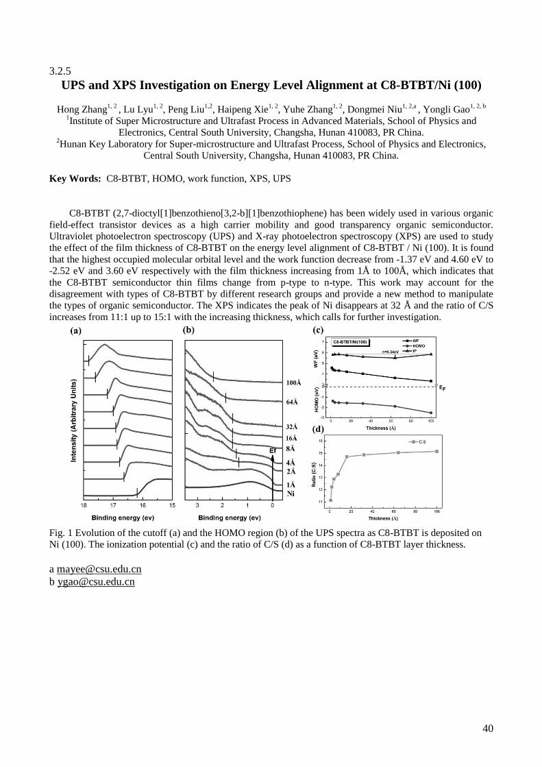
UPS and XPS Investigation on Energy Level Alignment at C8-BTBT/Ni (100)
Hong Zhang1, 2
, Lu Lyu1, 2
, Peng Liu1,2
, Haipeng Xie1, 2
, Yuhe Zhang1, 2
, Dongmei Niu1, 2,a
, Yongli Gao1, 2, b
1Institute of Super Microstructure and Ultrafast Process in Advanced Materials, School of Physics and
Electronics, Central South University, Changsha, Hunan 410083, PR China. 2Hunan Key Laboratory for Super-microstructure and Ultrafast Process, School of Physics and Electronics,
Central South University, Changsha, Hunan 410083, PR China.
Key Words: C8-BTBT, HOMO, work function, XPS, UPS
C8-BTBT (2,7-dioctyl[1]benzothieno[3,2-b][1]benzothiophene) has been widely used in various organic
field-effect transistor devices as a high carrier mobility and good transparency organic semiconductor.
Ultraviolet photoelectron spectroscopy (UPS) and X-ray photoelectron spectroscopy (XPS) are used to study
the effect of the film thickness of C8-BTBT on the energy level alignment of C8-BTBT / Ni (100). It is found
that the highest occupied molecular orbital level and the work function decrease from -1.37 eV and 4.60 eV to
-2.52 eV and 3.60 eV respectively with the film thickness increasing from 1Å to 100Å, which indicates that
the C8-BTBT semiconductor thin films change from p-type to n-type. This work may account for the
disagreement with types of C8-BTBT by different research groups and provide a new method to manipulate
the types of organic semiconductor. The XPS indicates the peak of Ni disappears at 32 Å and the ratio of C/S
increases from 11:1 up to 15:1 with the increasing thickness, which calls for further investigation.
Fig. 1 Evolution of the cutoff (a) and the HOMO region (b) of the UPS spectra as C8-BTBT is deposited on
Ni (100). The ionization potential (c) and the ratio of C/S (d) as a function of C8-BTBT layer thickness.
41
4.1.1
High efficiency white organic light-emitting diodes using thermally activated
delayed fluorescent emitters (1 line spacing)
Yong Joo Cho1, Bo Seong Kim
1, Kyoung Soo Yook
2, Jun Yeob Lee
1,a), b)
1Department of Polymer Science and Engineering, Dankook University, Korea
2School of Chemical Engineering, Sungkyunkwan University, Korea
(1 line spacing)
Keywords: high efficiency, thermally activated delayed fluorescence, white device, blue device,.
(2 line spacing)
Thermally activated delayed fluorescent devices have been actively developed for the last couple
of years because of the merit of high efficiency of the thermally activated delayed fluorescent
emitters. High efficiency close to 30% has been already demonstrated by optimizing the host
materials and device structure of the thermally activated delayed fluorescent devices. Therefore, the
thermally activated delayed fluorescent devices can catch up with state of the art phosphorescent
organic light-emitting diodes in terms of external quantum efficiency. The high quantum efficiency
of the thermally activated delayed fluorescent device can diversify the application and high
efficiency white organic light-emitting diodes can be fabricated using the thermally activated delayed
fluorescent emitters because the thermally activated delayed fluorescent emitters are compatible with
phosphorescent emitters.
In this work, we developed white organic light emitting diodes by combining a thermally
activated delayed fluorescent emitter with phosphorescent emitters. Various device structure
containing both the thermally activated delayed fluorescent emitters and phosphorescent emitters
were designed to optimize the device performances of the white organic light-emitting diodes. High
quantum efficiency above 20% was demonstrated using the newly developed blue thermally
activated delayed fluorescent emitter in the cool and warm white devices.
a) Presenting author’s Email : [email protected]
b) Corresponding author’s Email : [email protected]
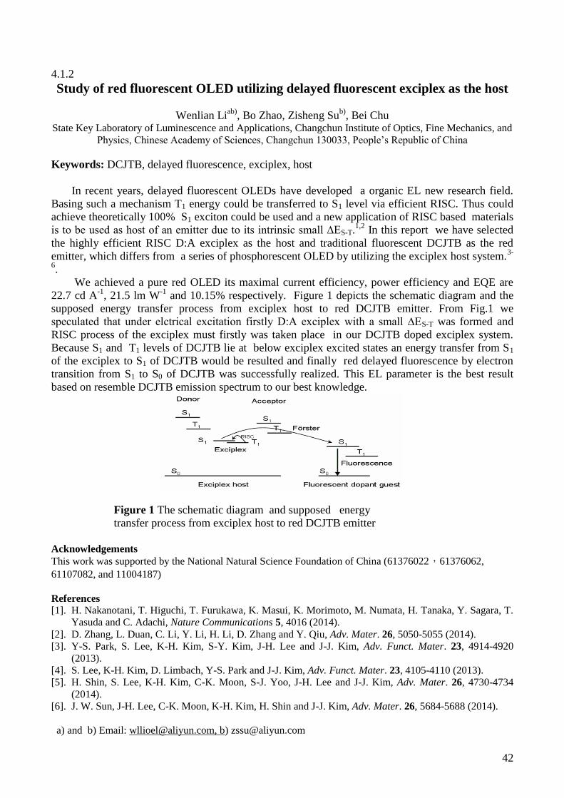
42
4.1.2
Study of red fluorescent OLED utilizing delayed fluorescent exciplex as the host
Wenlian Liab)
, Bo Zhao, Zisheng Sub)
, Bei Chu
State Key Laboratory of Luminescence and Applications, Changchun Institute of Optics, Fine Mechanics, and
Physics, Chinese Academy of Sciences, Changchun 130033, People’s Republic of China
Keywords: DCJTB, delayed fluorescence, exciplex, host
In recent years, delayed fluorescent OLEDs have developed a organic EL new research field.
Basing such a mechanism T1 energy could be transferred to S1 level via efficient RISC. Thus could
achieve theoretically 100% S1 exciton could be used and a new application of RISC based materials
is to be used as host of an emitter due to its intrinsic small ∆ES-T.1,2
In this report we have selected
the highly efficient RISC D:A exciplex as the host and traditional fluorescent DCJTB as the red
emitter, which differs from a series of phosphorescent OLED by utilizing the exciplex host system.3-
6.
We achieved a pure red OLED its maximal current efficiency, power efficiency and EQE are
22.7 cd A-1
, 21.5 lm W-1
and 10.15% respectively. Figure 1 depicts the schematic diagram and the
supposed energy transfer process from exciplex host to red DCJTB emitter. From Fig.1 we
speculated that under elctrical excitation firstly D:A exciplex with a small ∆ES-T was formed and
RISC process of the exciplex must firstly was taken place in our DCJTB doped exciplex system.
Because S1 and T1 levels of DCJTB lie at below exciplex excited states an energy transfer from S1
of the exciplex to S1 of DCJTB would be resulted and finally red delayed fluorescence by electron
transition from S1 to S0 of DCJTB was successfully realized. This EL parameter is the best result
based on resemble DCJTB emission spectrum to our best knowledge.
Figure 1 The schematic diagram and supposed energy
transfer process from exciplex host to red DCJTB emitter
Acknowledgements
This work was supported by the National Natural Science Foundation of China (61376022,61376062,
61107082, and 11004187)
References
[1]. H. Nakanotani, T. Higuchi, T. Furukawa, K. Masui, K. Morimoto, M. Numata, H. Tanaka, Y. Sagara, T.
Yasuda and C. Adachi, Nature Communications 5, 4016 (2014).
[2]. D. Zhang, L. Duan, C. Li, Y. Li, H. Li, D. Zhang and Y. Qiu, Adv. Mater. 26, 5050-5055 (2014).
[3]. Y-S. Park, S. Lee, K-H. Kim, S-Y. Kim, J-H. Lee and J-J. Kim, Adv. Funct. Mater. 23, 4914-4920
(2013).
[4]. S. Lee, K-H. Kim, D. Limbach, Y-S. Park and J-J. Kim, Adv. Funct. Mater. 23, 4105-4110 (2013).
[5]. H. Shin, S. Lee, K-H. Kim, C-K. Moon, S-J. Yoo, J-H. Lee and J-J. Kim, Adv. Mater. 26, 4730-4734
(2014).
[6]. J. W. Sun, J-H. Lee, C-K. Moon, K-H. Kim, H. Shin and J-J. Kim, Adv. Mater. 26, 5684-5688 (2014).
a) and b) Email: [email protected], b) [email protected]

43
4.1.3
Development of Host and Dopant Materials for Phosphorescent Organic Light-
Emitting Diodes
Jiuyan Li1,a)
, Wei Li1, Fang Wang
1
1 State key laboratory of fine chemicals, school of chemical engineering, Dalian university of
technology, 2 Linggong Road, Dalian 116024, CHINA.
Keywords: OLEDs, electrophosphorescence, host materials, iridium phosphors, dopant
Electrophosphorescence is advantageous over the traditional electrofluorescence in terms of
emission efficiency since all triplet and singlet excitons generated by charge recombination in
phosphorescent organic light-emitting diodes (OLEDs) can be harvested for light emission.
Organometallic iridium(III) complexes have been established as the most efficient phosphors for use
in OLEDs. In order to avoid emission quenching in neat films, the phosphorescent devices usually
adopt host-dopant configuration in the emitting layer. The doped phosphor is typically excited
through energy transfer from host or direct charge trapping by dopant. Therefore, both host materials
and the iridium phosphors play essential role in determining the overall device performance. In this
lecture, both organic host materials and novel iridium complexes developed in author’s group in
recent years will be reported.
For iridium phosphors, the molecular structures are designed and modified for the purpose of
optimizing emission efficiency. It was observed that the decoration of the cyclometalating ligands by
fluorine atom (F) and trifluoromethyl groups (CF3) are effective strategy to improve phosphorescent
efficiency of the iridium complexes.[1]
Extremely high efficiencies were achieved for both the single
color and white OLEDs using those F and CF3 decorated iridium phosphores as light emitters.[1,2]
Furthermore, multi-fluorination of the cyclometalating ligands was demonstrated as a powerful
strategy to achieve highly efficient tris-cyclometalated iridium phosphors. A high efficiency of over
90 cd/A was obtained for the green phosphorescent OLEDs at an extremely high brightness of 10000
cd/m2. In addition, the color-tuning behavior of iridium phosphors was also studied.
The host materials in doped phosphorescent OLEDs not only contribute to the overall device
performance, but also determine the fabrication technique. Three types of host materials, i.e., high-
triplet-energy hosts, bipolar hosts, and solution processible hosts, will be mainly discussed in this
report. To possess as high triplet energy is the prerequisite for the host materials to guarantee the
efficient forward energy transfer in phosphorescent OLEDs. How to control the molecular
conjugation by adjusting the molecular conformation will be the most import issue to lead to high
triplet energies.[3]
For bipolar host materials, the selection of appropriate groups as the n-type units
still remains as the most important challenge. We have explored various CN-decorated aromatic
groups and the triazole and benzotriazole as the ideal n-type units to build up novel bipolar host
materials for phosphorescent OLEDs.[4]
Solution processing seems to be the most ideal and final
device fabrication technique for practical applications due to its easiness and low-cost. A series of
carbazole-based dendrimers have been developed as solution processible host materials for use in
phosphorescent OLEDs. The influence of the generation of dendrimer hosts to the device
performance will be focus of discussion.[5]
[1] R Wang, D. Liu, H. Ren, J. Li, Adv. Mater., 2011, 23, 2823-2827.
[2] R Wang, D Liu, T. Zhang, J. Li, J. Mater. Chem., 2011, 21, 15494-15500.
[3] L. Deng, X. Wang, J. Li, J. Mater. Chem., 2012, 22, 19700-19708.
[4] L. Deng, J. Li, G. Wang, L. Wu, J. Mater. Chem. C, 2013, 1, 8140-8145.
[5] J. Li, T. Zhang, Y. Liang, R. Yang, Adv. Funct. Mater., 2013, 23, 619-628.
a) Presenting author and Corresponding author’s Email: [email protected]
44
4.1.4
Novel Bipolar Host Materials for Phosphorescent and TADF OLEDs
Di Liu1,a)
, Miao Wang1, Ruijuan Yao
1
1 State key laboratory of fine chemicals, School of chemistry, Dalian university of technology, 2
Linggong Road, Dalian 116024, CHINA.
Keywords: Organic Light-Emitting Diodes (OLEDs), thermally activated delayed fluorescence
(TADF), electrophosphorescence, bipolar host materials
Organic light-emitting diodes (OLEDs) technique is drawing more and more research attentions
from both academic and industrial fields due to their promissing applications as new-generation flat-
panel display and solid-state lighting source. In order to fulfill the demand of practical applications,
the most important issues of OLEDs research for the time being include to further increase the
energy conversion efficiency, to improve the device stability, and to reduce the device fabrication
cost. Electrophosphorescence is well known for its advantage over the conventional
electrofluorescence in terms of emission efficiency since all triplet and singlet excitons generated by
charge recombination can be harvested for light emission. In recent years, the thermally activated
delayed fluorescence (TADF) phenomenum has emerged as a hot-spot in OLEDs research field.[1]
The OLEDs based on TADF emitters are as attractive as electrophosphorescent devices due to their
theoretical internal quantum efficiency limit of unity by counting both prompt fluorescence and
thermally activated delayed fluorescence via efficient reverse intersystem crossing. However, TADF
emitters are superior and have more sustainability since they avoid to use noble rare metals. In both
phosphorescent and TADF OLEDs, doping strategy is necessary to avoid unwanted triplet-triplet
annihilation quenching. The host matrix is as important as the doped emitter to determine the overall
device performance since it occupies the majority of the emitting layer in the OLEDs.[2]
Bipolar host materials have been proved to be capable of balancing charge transportation in the
emitting layer and consequently leading to high emission efficiency and suppressing efficiency roll-
off.[3]
Since the electron transporting mobility of most of the concurrent organic n-type materials or
functional groups are lower by two to three orders of magnitude than those of the p-type materials, to
select appropriate n-type functional units always remains as one of the challenges to construct ideal
bipolar host materials. In this presentation, the author will report the latest progress of designing
novel bipolar host materials in the author’s group. The focus will be placed on the exploration of
various n-type units to construct bipolar molecules. Three types of functional groups have been
explored to act as n-type units in bipolar host materials, i.e., cyano-decorated aromatic groups,
triazole and benzotriazole, and pyridyl or composite pyridyl with other strong electron-withdrawing
groups. All these novel bipolar host materials have been used to fabricate phosphorescent OLEDs
with various iridium phosphors as doped emitters and most of them exhibited satisfied
electroluminescence performance. And most of them have also been used as host materials for
TADF OLEDs with commercial available TADF molecules as emitters, some of which then gave
excellent emission efficiency. It was proved that CN-decorated aromatic groups and trizaole and
substituted pyridyl are all ideal n-type units for bipolar host materials. In particular, it was observed
that benzotriazole, in comparison with triazole, is not a good candidate to build up bipolar molecules
since they tend to decompose as shown in mass spectra and OLED study.
[1] H. Uoyama, K. Goushi, K. Shizu, H. Nomura, C. Adachi, Nature, 2012, 492, 234.
[2] J. Li, T. Zhang, Y. Liang, R. Yang, Adv. Funct. Mater., 2013, 23, 619-628.
[3] A. Chaskar, H.-F. Chen, K.-T. Wong, Adv. Mater. 2011, 23, 3876.
a) Presenting author and Corresponding author’s Email: [email protected]
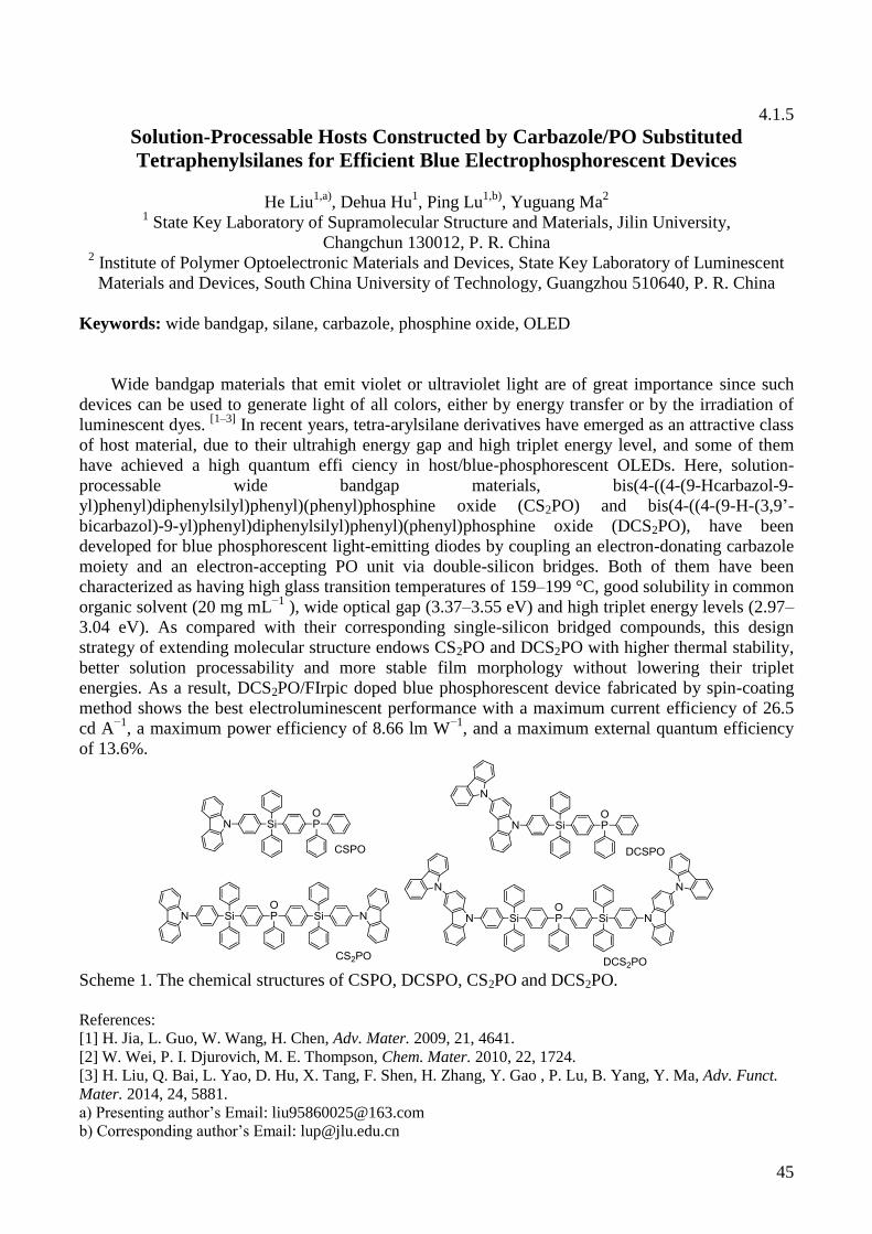
45
4.1.5
Solution-Processable Hosts Constructed by Carbazole/PO Substituted
Tetraphenylsilanes for Efficient Blue Electrophosphorescent Devices
He Liu1,a)
, Dehua Hu1, Ping Lu
1,b), Yuguang Ma
2
1 State Key Laboratory of Supramolecular Structure and Materials, Jilin University,
Changchun 130012, P. R. China 2 Institute of Polymer Optoelectronic Materials and Devices, State Key Laboratory of Luminescent
Materials and Devices, South China University of Technology, Guangzhou 510640, P. R. China
Keywords: wide bandgap, silane, carbazole, phosphine oxide, OLED
Wide bandgap materials that emit violet or ultraviolet light are of great importance since such
devices can be used to generate light of all colors, either by energy transfer or by the irradiation of
luminescent dyes. [1–3]
In recent years, tetra-arylsilane derivatives have emerged as an attractive class
of host material, due to their ultrahigh energy gap and high triplet energy level, and some of them
have achieved a high quantum effi ciency in host/blue-phosphorescent OLEDs. Here, solution-
processable wide bandgap materials, bis(4-((4-(9-Hcarbazol-9-
yl)phenyl)diphenylsilyl)phenyl)(phenyl)phosphine oxide (CS2PO) and bis(4-((4-(9-H-(3,9’-
bicarbazol)-9-yl)phenyl)diphenylsilyl)phenyl)(phenyl)phosphine oxide (DCS2PO), have been
developed for blue phosphorescent light-emitting diodes by coupling an electron-donating carbazole
moiety and an electron-accepting PO unit via double-silicon bridges. Both of them have been
characterized as having high glass transition temperatures of 159–199 °C, good solubility in common
organic solvent (20 mg mL−1
), wide optical gap (3.37–3.55 eV) and high triplet energy levels (2.97–
3.04 eV). As compared with their corresponding single-silicon bridged compounds, this design
strategy of extending molecular structure endows CS2PO and DCS2PO with higher thermal stability,
better solution processability and more stable film morphology without lowering their triplet
energies. As a result, DCS2PO/FIrpic doped blue phosphorescent device fabricated by spin-coating
method shows the best electroluminescent performance with a maximum current efficiency of 26.5
cd A−1
, a maximum power efficiency of 8.66 lm W−1
, and a maximum external quantum efficiency
of 13.6%.
Scheme 1. The chemical structures of CSPO, DCSPO, CS2PO and DCS2PO.
References:
[1] H. Jia, L. Guo, W. Wang, H. Chen, Adv. Mater. 2009, 21, 4641.
[2] W. Wei, P. I. Djurovich, M. E. Thompson, Chem. Mater. 2010, 22, 1724.
[3] H. Liu, Q. Bai, L. Yao, D. Hu, X. Tang, F. Shen, H. Zhang, Y. Gao , P. Lu, B. Yang, Y. Ma, Adv. Funct.
Mater. 2014, 24, 5881.
a) Presenting author’s Email: [email protected]
b) Corresponding author’s Email: [email protected]
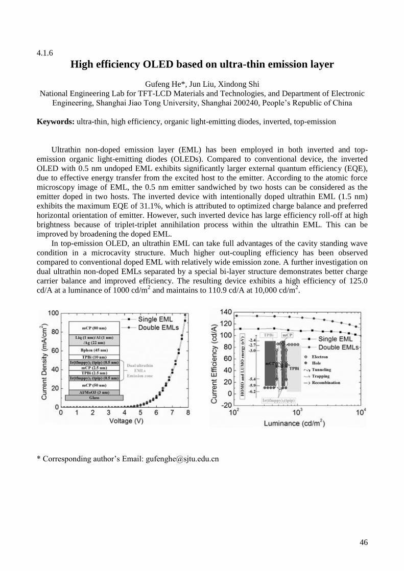
46
4.1.6
High efficiency OLED based on ultra-thin emission layer
Gufeng He*, Jun Liu, Xindong Shi
National Engineering Lab for TFT-LCD Materials and Technologies, and Department of Electronic
Engineering, Shanghai Jiao Tong University, Shanghai 200240, People’s Republic of China
Keywords: ultra-thin, high efficiency, organic light-emitting diodes, inverted, top-emission
Ultrathin non-doped emission layer (EML) has been employed in both inverted and top-
emission organic light-emitting diodes (OLEDs). Compared to conventional device, the inverted
OLED with 0.5 nm undoped EML exhibits significantly larger external quantum efficiency (EQE),
due to effective energy transfer from the excited host to the emitter. According to the atomic force
microscopy image of EML, the 0.5 nm emitter sandwiched by two hosts can be considered as the
emitter doped in two hosts. The inverted device with intentionally doped ultrathin EML (1.5 nm)
exhibits the maximum EQE of 31.1%, which is attributed to optimized charge balance and preferred
horizontal orientation of emitter. However, such inverted device has large efficiency roll-off at high
brightness because of triplet-triplet annihilation process within the ultrathin EML. This can be
improved by broadening the doped EML.
In top-emission OLED, an ultrathin EML can take full advantages of the cavity standing wave
condition in a microcavity structure. Much higher out-coupling efficiency has been observed
compared to conventional doped EML with relatively wide emission zone. A further investigation on
dual ultrathin non-doped EMLs separated by a special bi-layer structure demonstrates better charge
carrier balance and improved efficiency. The resulting device exhibits a high efficiency of 125.0
cd/A at a luminance of 1000 cd/m2 and maintains to 110.9 cd/A at 10,000 cd/m
2.
* Corresponding author’s Email: [email protected]

47
4.2.1
Graphene oxide derivatives as interface materials for polymer solar cells (1 line spacing)
Jian Zhang1,a)
, Dong Yang2, Lingyu Zhou
2, Can Li
2,
1Department of Material Science and Technology, Guangxi Key Laboratory of Information
Materials, Guilin University of Electronic Technology, 1# Jinji Road, 541004, Guilin, Guangxi,
China. 2tate Key Laboratory of Catalysis, Dalian Institute of Chemical Physics, Chinese Academy of
Sciences; Dalian National Laboratory for Clean Energy Dalian 116023, China
(1 line spacing)
Keywords: graphene oxide, derivatives, work function, interface material, polymer solar cell.
(2 line spacing)
Polymer solar cells (PSCs) represent an exciting class of renewable energy technology, and are
under intensive investigation in both academic institutions and industrial companies due to their
potential to enable mass production of flexible and cost-effective devices through roll-to-roll
techniques. The proper choice of interface materials is a must for highly efficient and stable PSC
devices and has become a significant part of the PSC research today. Interface materials are either
non-conducting, semiconducting or conducting layers which not only provide selective contacts for
carriers of one sort, but can also determine the polarity of PSC devices, affect the open-circuit
voltage, and act as optical spacers or protective layers.
Owing to their solution processability, unique two-dimensional structure, and functionalization-
induced tunable electronic structures, graphene oxide (GO) and its derivatives have been used as a
new class of efficient interface materials in polymer solar cells (PSCs). Highly efficient and stable
PSCs have been fabricated with GO and its derivatives as interface materials. In this talk, we will
summarize recent progress in this emerging research field. And then present our rational concepts for
the design and development of the GO-based interface materials for high performance PSCs.
Acknowledgement. This work was financially supported by the National Natural Science
Foundation of China under Grant No. 21374120.
References
(1) D. Yang, L. Y. Zhou, J. Zhang,* C. Li* et al., Chem. Comm., 2012, 48, 8078.
D. Yang, W. Yu, L. Zhou, J. Zhang,* C. Li*, Adv. Energy Mater. 2014 DOI:
10.1002/aenm.201400591.

48
4.2.2
Foldable composite circuit on paper toward stable operation of
top-emitting organic light emitting diodes
Sung Min Jo a)
, Byung Doo Chin b)
Dept. of Polymer Science and Engineering, Dankook University
Jukjeon-dong, Suji-gu, Yongin-City, Gyeonggi-do, 448-701, Republic of Korea
Keywords: paper, top emission, OLED, foldable.
Foldable and flexible electronics are not only an important but also a promising issue for the
convenient transportation and diverse deployment of mobile displays. Composite electrodes with
metallic patterns [1] and graphene nanoplate-based circuits prepared on the paper substrate by simple
transfer printing [2] showed an unique, small change in conductance under various folding angles,
retaining more than 80% of initial conductance. In this paper, improved uniformity and printability
of the flexible electrode on the surface of commercial paper substrates are illustrated. Due to the lack
of transparency for this paper-based substrate, we have fabricated top-emitting organic light emitting
diode (TOLED), where its light emitting behavior and efficiency was investigated in terms of the
surface composition of paper and its functionality. In order to realize a foldable and deformable
display, printed circuits should be also robust under repeated operation. Therefore, such paper
surfaces were planarized by using several polymeric over-coating layers [poly vinyl alcohol (PVA),
poly(4-vinylphenol)(PVP), etc.] in order to reduce the roughness as well as provide a good
deposition and printing condition for the electrode patterns. Silver electrode was fabricated onto
paper either by thermal evaporation or inkjet printing. Complex electrode of silver nanowires and
graphene was fabricated onto planarized paper. It was confirmed that stability of electrode at
repeated folding test was obtained with a -180 o ~ +180
o folding angles, showing the possibility of its
application as a foldable electrode. We have investigated the improvement of conductance of
graphene electrode by the addition of silver nanowires. Top emitting OLED was prepared by thermal
evaporation on paper, with Al/ molybdenum oxide (MoO3)/ N,N-di(naphthalene-1-yl)-N,N-
diphenyl-benzidine(NPB)/ Tris-(8-hydroxy-quinoline)aluminum (Alq3) / LiF/ Al/ Ag. OLEDs with
evaporated silver, printed Ag interconnecting circuit, and graphene composite electrode were
characterized in terms of the condition of modified paper surface and corresponding circuits. Our
approach will be a facile and cost-effective strategy for foldable and flexible OLEDs toward
application such as disposable electronics and digital signages.
-180 -90 0 90 180
0.0
0.2
0.4
0.6
0.8
1.0
Rati
o o
f co
nd
ucta
nce(G
/G0)
Folding andgle (o)
Ag nanowires
10wt% graphene of Ag nws
30wt% graphene of Ag nws
Fig 1. Ratio of conductance vs. folding angles of interconnecting electrode, and image of top
emitting OLED at folded substrate References
1. A. C. Siegel, S. T. Phillips , M. D. Dickey , N. Lu , Z. Suo , G. M. Whitesides, Adv. Funct. Mater. 20, 28
(2010)
2. W. J. Hyun, O O. Park, B. D. Chin, Adv. Mater. 25, 4729 (2013)

49
4.2.3
Interfacial Engineering with Biomolecules for High Performance Organic and
Hybrid devices
Riming Nie, Aiyuan Li, Yangyang Wang, Zejia Zhao, Xianyu Deng a), b)
Department of Materials and Engineering, Harbin Institute of Technology Shenzhen Graduate
School, Shenzhen, 518055
Keywords: Organic Electronics, Hybrid Electronics, Interfaces, Biomaterials, Metal Oxides
Biomolecules of amino acids and peptides act as an ideal interfacial material on the surface of
metal oxides, such as indium tin oxide (ITO) and titanium dioxide (TiO2). Work function of these
modified surfaces shows an effective reduction to promote electron transfer at organic/metal oxide
interfaces in organic or organic-inorganic hybrid devices. These lead to a significant enhancement on
performance for various organic based devices, including organic light-emitting diodes, solar cells
and photodetectors.
a) and b) Presenting and Corresponding author’s Email: [email protected]

50
4.2.4
High-performance biosensors based on organic thin film transistors
Feng Yan1,a)
, 1Depaetment of Applied Physics, The Hong Kong Polytechnic University, Hong Kong
Keywords: Organic thin film transistor, biosensor, cell, DNA.
Solution-gated organic thin film transistors have shown promising applications in biosensors due
to the high sensitivity, low working voltage and the simple design of the devices. Solution-gated
transistors normal have no gate dielectric and the gate voltages are applied directly on the
solid/electrolyte interfaces or electric double layers near the channel and the gate, which lead to very
low working voltages (about 1 V) of the transistors. On the other hand, the devices can be easily
prepared by solution process or other convenient methods because of the much simpler device
structure compared with that of a conventional field effect transistor with several layers. Many
biosensors can be developed based on the detection of potential changes across solid/electrolyte
interfaces induced by electrochemical reactions or interactions. The devices normally can show high
sensitivity due to the inherent amplification function of the transistors. Here, I will introduce several
types of biosensors studied by our group recently, including DNA[1], glucose[2], dopamine, uric
acid, cell[3], and bacteria sensors, based on solution-gated organic electrochemical transistors or
graphene transistors[4]. The biosensors show high sensitivity and selectivity when the devices are
modified with functional nano-materials (e.g. graphene, Pt nanoparticles) and biomaterials (e.g.
enzyme, antibody, DNA) on the gate electrodes or the channel. Furthermore, the devices are
miniaturized successfully for the applications as sensing arrays. It is expected that the solution-gated
transistors will find more important applications in the future..
a) Presenting author’s Email: [email protected]

51
4.2.5
The smallest (so far) pure-carbon logic operators
Xiao-Hong Yan1,2,3,a),b)
, Yan-Dong Guo1,2
, Yang Xiao3, Chun-Sheng Liu
1,2
1 College of Electronic Science and Engineering, Nanjing University of Posts and
Telecommunications, Nanjing 210046, China, 2 Key Laboratory of Radio Frequency and Micro-
Nano Electronics of Jiangsu Province, Nanjing 210023, Jiangsu, China, 3 College of Science,
Nanjing University of Aeronautics and Astronautics, Nanjing 210016, China
Keywords: molecular device; electronic transport; pure-carbon device; logic operator
The pure-carbon nanoscale device is a promising research area in the next-generation nano
devices. Recently, the pure-carbon structures of graphene(benzene)–chain–graphene(benzene) have
been synthesized experimentally. Based on first-principles calculation, we investigate the electronic
transport properties of such two–one–two dimensional carbon systems. Switching behavior induced
by conformational changes is observed, even for the systems with curved and quite long carbon
chains. The spatial asymmetry of transmission channels between one- and two-dimensional carbon
structures is found to be the physical mechanism behind this behavior, and it can be extended to
metal systems. It is also found that the orientation of a transmission channel is able to be rotated by a
nanotube (or curved graphene) through the non-planar p-conjugated orbitals to modulate the
switching behavior. Based on these structures, a kind of extremely-small pure-carbon logic operators
and some other devices are proposed. As atomic motion could process information directly, the
switching behavior and those devices show great application potential in nanomechanics.
a),b) [email protected]

52
4.2.6
Engineering of Materials for Flash Memory and Sensors
V. A. L. Roy
Department of Physics and Materials Science and Center of Super-Diamond and Advanced Films
(COSDAF), City University of Hong Kong, Hong Kong SAR.
Keywords: Flash memory, Floating gate and TFT sensors.
The next-generation electronic systems are expected to be light, flexible and portable for
applications in large area displays, integrated circuits (ICs), radio frequency identification (RFID)
tags, solar cells and so on. Memory is an essential part of advanced electronic systems for data
processing, storage and communication. Among many types of memories such as ferroelectric,
electret, resistive and floating gate, nano-floating gate flash memory devices have gained a great deal
of attention due to the simple device structure, non-destructive read-out and controlled trap capacity.
In this presentation, we will explain our recent work on non-volatile flash memories and its
prototypes. In addition, we discuss on CMOS based sensors for the sensitive and selective detection
of bio-genic amines for food safety.
Corresponding author’s Email [email protected]

53
5.1
Perovskite Solar Cell
Nam-Gyu Park
School of Chemical Engineering, Sungkyunglwan University, Suwon 440-746, Korea
Keywords: organolead halide, perovskite, solar cell, high efficiency, size control
Perovskite solar cell based on organo lead halide light harvester is an emerging photovoltaic
technology due to extremely low cost and superb photovoltaic performance. In this talk,
fundamentals and technologies for high efficiency perovskite solar cells are discussed. Since the first
report on a long-term durable perovskite solar cell with a poer conversion (PCE) of 9.7% in 2012,
researches on perovskite solar cells are triggered. As a result PCE approaches 20% in 2014.
CH3NH3PbI3 (MALI) and HC(NH2)2PbI3 (FALI) are typical materials for high efficiency perovskite
solar cells. Due to the unbalanced diffusion length between free electrons and holes, mesoporous
TiO2 layer is found to extend diffusion of electrons in both MALI and FALI. However, difference in
electron mobility between TiO2 and perovskite may lead to poor charge collection. ZnO nanorod is
found to be better than TiO2 in terms of electron collection. Photovoltaic parameters depend
significantly on perovskite crystal size. Large size is beneficial to charge extraction and dipole
relaxation. Morphology and size are critical in achieving high performance. PCEs of 17% and 16%
are achieved from MALI and FALI, respectively, by controlling morphology and crystal size.
Interfacial nanoengineering is also found to be important in terms of charge recombination control
and charge collection.
a) Presenting author’s Email: [email protected]
b) Corresponding author’s Email: [email protected]
54
5.2
Nickel oxide p-type electrode interlayer in CH3NH3PbI3 perovskite/fullerene
planar-heterojunction hybrid solar cells
Jun-Yuan Jeng, Kuo-Cheng Chen, Tsung-Yu Chiang, Tzung-Fang Guo a)
, and Peter Chen Department of Photonics, Advanced Optoelectronic Technology Center, Research Center for Energy
Technology and Strategy, National Cheng Kung University,
No. 1 Ta-Hsueh Rd., Tainan, Taiwan 701
Keywords: perovskite, nickel oxide, p-type, planar-heterojunction, solar cells
The work presented the application of nickel oxide as the p-contact to fabricate the decent
perovskite-based photovoltaics.1-3
The p-type nickel oxide exhibits several optical, electrical, and
chemical advantages being the potential electrode-interlayer. A respectful solar to electrical PCE of
7.8% with a VOC = 0.92 V, a JSC = 12.43 mA/cm2, and a FF = 0.68 has been achieved with the device
configuration of the glass/ITO/NiOx/CH3NH3PbI3 perovskite/PCBM/BCP/Al structure under
standard 1 sun AM 1.5G simulated solar irradiation.1 In addition, the device composed of the
mesoscopic nanocrystalline NiO/peroskite/PCBM configuration exhibits a VOC = 0.96 V, a JSC = 19.8
mA/cm2, and a FF = 0.61, corresponding to a higher magnitude of PCE to 11.6%.
3
NiO electrode interlayer is a p-type semiconductor of high work function of 5.4 eV, which is
close to the valence band edge level of CH3NH3PbI3 perovskite (5.4 eV). The alignment of energy
level minimizes the interfacial energy losses for the hole transfer and optimizes the photovoltage
output of device. Additionally, the higher magnitude of JSC and PCE also results from the better
surface coverage of CH3NH3PbI3 perovskite film on the glass/ITO/NiOx substrate.1 The efficient hole
transfer at perovskite/NiO heterojunction was verified by photo-induced absorption spectroscopy,
showing a broad spectral feature above 800 nm, the long-lived charge-separation state of NiO+/P
-.2
The success of this new style device configuration of p-type metal oxide material has the advantages
of providing robust perovskite-based thin film solar cells in future. Our findings reveal the design
principle for enhancing the photovoltaic performance of CH3NH3PbI3 perovskite/PCBM hybrid
PHJ4,5
solar cells through the judicious selection of the metal oxide electrode interlayer.
References 1. J. –Y. Jeng, K. –C. Chen, T. –Y. Chiang, P. –Y. Lin, T. –D. Tsai, Y. –C. Chang, T. –F. Guo, and P. Chen "Nickel oxide
electrode interlayer in CH3NH3PbI3 perovskite/PCBM planar-heterojunction hybrid solar cells" Adv. Mater. 26, 4107
(2014).
2. K. –C. Wang, J. –Y. Jeng, P. –S. Shen, Y. –C. Chang, E. W. –G. Diau, C. –H. Tsai, T. Y. Chao, H. –C. Hsu, P. –Y. Lin,
P. Chen, T. –F. Guo, and T. –C. Wen "p-type Mesoscopic nickel oxide/organometallic perovskite heterojunction solar
cells " Sci. Rep. 4, 4765 (2014).
3. K. –C. Wang, P. –S. Shen, M. –H. Li, S. Chen, M. –W. Lin, P. Chen, and T. –F. Guo "Low temperature sputtered
nickel oxide compact thin film as effective electron blocking layer for mesoscopic NiO/CH3NH3PbI3 perovskite
heterojunction solar cells" ACS Appl. Mater. Inter. 6, 11851 (2014).
4. J. –Y. Jeng, Y. –F. Chiang, M. –H. Lee, S. –R. Peng, T. –F. Guo, P. Chen, and T. –C. Wen "CH3NH3PbI3
perovskite/fullerene planar-heterojunction hybrid solar cells" Adv. Mater. 25, 3727 (2013).
5. Y. –F. Chiang, J. –Y. Jeng, M. –H. Lee, S. –R. Peng, P. Chen, T. –F. Guo, T. –C. Wen, Y. –J. Hsu, C. –M. Hsu "High
voltage and efficient bilayer heterojunction solar cells based on organic-inorganic hybrid perovskite absorber with
low-cost flexible substrate " Phys. Chem. Chem. Phys. 16, 6033 (2014).
a)

55
5.3
Electrode Buffer Layer Materials for High Performance Polymer Solar Cells
Yongfang Li
Institute of Chemistry, Chinese Academy of Sciences, Beijing 100190, China
e-mail: [email protected]
Keywords: polymer solar cells, cathode buffer layer, anode buffer layer.
Bulk-heterojunction polymer solar cells (PSCs) have attracted great attention in recent years,
because of their advantages of low cost fabrication, light weight and flexibility. For achieving higher
power conversion efficiency of the PSCs, great efforts have been devoted to the design and synthesis
of new donor and acceptor photovoltaic materials, [1]
new cathode and anode buffer layer materials,
and new device structures. In this presentation, I will talk about our recent progress on the solution-
processable cathode and anode buffer layer materials. The cathode buffer layers we developed
include metal chelates TIPD[2]
and ZrAcac[3]
, hyperbranched polymer[4]
, C60 derivatives[5]
and n-type
organic molecules[6]
with side chains containing amine end groups. The anode buffer layer materials
are a series of metal oxides[7]
obtained by thermal annealing their solution-processed precursors at
lower temperature. The PSCs with the anode or cathode buffer layers showed improved photovoltaic
performance and high stability. In addition, some buffer layer materials mentioned above have been
successfully applied in high performance organic-inorganic hybrid perovskite solar cells.
References:
[1] Y. F. Li, Acc. Chem. Res. 2012, 45, 723–733..
[2] Z. A. Tan, W. Q. Zhang, Y. Huang, Z. G. Zhang, D. P. Qian, J. H. Hou, Y. F. Li, Adv. Mater. 2012, 24,
1476-1481.
[3] Z. A. Tan, S. S. Li, F. Z. Wang, D. P. Qian, J. Lin, J. H. Hou, Y. F. Li, Scientific Report, 2014, 4, 4691
[4] M. L. Lv, S. S. Li, J. Jasieniak, J. H. Hou, S. E. Watkins, J. Zhu, Z. A. Tan, Y. F. Li, X. W. Chen, Adv.
Mater., 2013, 25, 6889–6894.
[5] S. S. Li, M. Lei, M. L. Lv, S. E. Watkins, Z. A. Tan, J. Zhu, J. H. Hou, X. W. Chen, Y. F. Li, Adv. Energy
Mater. 2013, 3, 1569–1574.
[6] Z.-G. Zhang, B. Y. Qi, Z. W. Jin, D. Chi, Z. Qi, Y. F. Li, J. Z. Wang, Energy Environ. Sci., 2014, 7, 1966-
1973
[7] (a) F. Z. Wang, Q. Xu, Z. A. Tan, L. J. Li, S. S. Li, X. L. Hou, G. Sun, X. H. Tu, J. H. Hou, Y. F. Li, J.
Mater. Chem. A, 2014, 2, 1318-1324. (b) X. H. Tu, F. Z. Wang, C. Li, Z. A. Tan, Y. F. Li, J. Phys. Chem.
C, 2014, 118, 9309-9317. (c) Z. A. Tan, L. J. Li, F. Z. Wang, Q. Xu, S. S. Li, G. Sun, X. H. Tu, X. L.
Hou, J. H. Hou, Y. F. Li, Adv. Energy Mater. 2014, 4, 1300884.
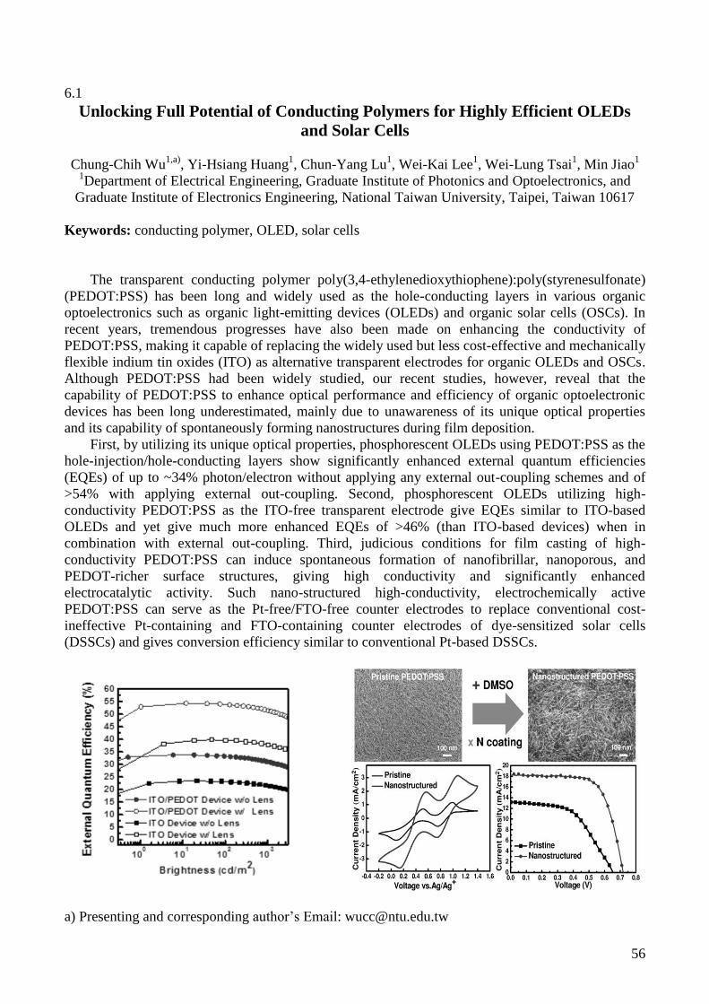
56
6.1
Unlocking Full Potential of Conducting Polymers for Highly Efficient OLEDs
and Solar Cells
Chung-Chih Wu1,a)
, Yi-Hsiang Huang1, Chun-Yang Lu
1, Wei-Kai Lee
1, Wei-Lung Tsai
1, Min Jiao
1
1Department of Electrical Engineering, Graduate Institute of Photonics and Optoelectronics, and
Graduate Institute of Electronics Engineering, National Taiwan University, Taipei, Taiwan 10617
Keywords: conducting polymer, OLED, solar cells
The transparent conducting polymer poly(3,4-ethylenedioxythiophene):poly(styrenesulfonate)
(PEDOT:PSS) has been long and widely used as the hole-conducting layers in various organic
optoelectronics such as organic light-emitting devices (OLEDs) and organic solar cells (OSCs). In
recent years, tremendous progresses have also been made on enhancing the conductivity of
PEDOT:PSS, making it capable of replacing the widely used but less cost-effective and mechanically
flexible indium tin oxides (ITO) as alternative transparent electrodes for organic OLEDs and OSCs.
Although PEDOT:PSS had been widely studied, our recent studies, however, reveal that the
capability of PEDOT:PSS to enhance optical performance and efficiency of organic optoelectronic
devices has been long underestimated, mainly due to unawareness of its unique optical properties
and its capability of spontaneously forming nanostructures during film deposition.
First, by utilizing its unique optical properties, phosphorescent OLEDs using PEDOT:PSS as the
hole-injection/hole-conducting layers show significantly enhanced external quantum efficiencies
(EQEs) of up to ~34% photon/electron without applying any external out-coupling schemes and of
>54% with applying external out-coupling. Second, phosphorescent OLEDs utilizing high-
conductivity PEDOT:PSS as the ITO-free transparent electrode give EQEs similar to ITO-based
OLEDs and yet give much more enhanced EQEs of >46% (than ITO-based devices) when in
combination with external out-coupling. Third, judicious conditions for film casting of high-
conductivity PEDOT:PSS can induce spontaneous formation of nanofibrillar, nanoporous, and
PEDOT-richer surface structures, giving high conductivity and significantly enhanced
electrocatalytic activity. Such nano-structured high-conductivity, electrochemically active
PEDOT:PSS can serve as the Pt-free/FTO-free counter electrodes to replace conventional cost-
ineffective Pt-containing and FTO-containing counter electrodes of dye-sensitized solar cells
(DSSCs) and gives conversion efficiency similar to conventional Pt-based DSSCs.
a) Presenting and corresponding author’s Email: [email protected]

57
6.2
Thermochromism Study of Low Band-Gap Photovoltaic Polymers Chin-Ti Chen
Institute of Chemistry, Academia Sinica, Taipei 11529, Taiwan, ROC
A series of low band-gap copolymers (pBCN copolymers) based on benzo(1,2-b:4,5-b’)dithiophene
donor and thienylcyanovinyl acceptor anchored with different number and shape of solubilizing alkyl
chains were designed and synthesized. The implication of alkyl chains and - interaction on
polymer aggregations was investigated by temperature-dependent UV-visible absorption and IR
spectroscopy. Via grafting appropriate alkyl side-chain substituent on different position of the
copolymer main chain, thermochromic phenomena are controllable both in the solution and in the
thin film state. The results from the thermochromism study of these copolymers agrees with the
enhancement of photovoltaic performances through the solvent annealing treatment reported
previously.1 Currently, by extending solvent annealing time to 60 minutes and adopting inverted
device structure, power conversion efficiency of pBCN4/PC71BM bulk heterojunction OPV has been
improved from 4.9% to 6.2% .
0.0 0.2 0.4 0.6 0.8 1.0-14
-12
-10
-8
-6
-4
-2
0
2
ITO / ZnO / pBCN4:PC71
BM / MoO3 / Ag
Voltage (V)
C
urr
ent
Den
sity (
mA
/cm
2)
pBCN4, 1:1.5, w/o SA
pBCN4, 1:1.5, w/ SA
400 500 600 700 800
0
10
20
30
40
50
60
70
80
90ITO / ZnO / pBCN4:PC
71BM / MoO
3 / Ag
pBCN4, w/o SA
pBCN4, w/ SA
Wavelength [nm]
EQ
E [
%]
References
1. Chen, H. -Y.; Wu, J. -L; Chen, C.-T.; Chen, C.-T., Chem. Commun. 2012, 48, 1012.

58
6.3
Functional Molecular Materials – From Design to Functions and Applications
Vivian Wing-Wah Yam
Department of Chemistry, The University of Hong Kong, Pokfulam Road, Hong Kong
Keywords: metal complexes, OLEDs, solar cells
There has been considerable growth of interest in new functional molecular materials with
unique properties for technological developments. Functional molecular materials can be found in all
classes of materials for specific applications, including optoelectronics, electronics, photonics,
sensors, magnetics, memories and others. Of particular interest is the design of metal-organic
compounds with interesting luminescence properties for the applications in organic light-emitting
devices (OLEDs) as well as organic and metal-organic materials with strong light-harvesting
properties for the applications in organic photovoltaic (OPV) devices. In this work, various design
and synthetic strategies to generate new classes of functional molecular materials will be described.
Through a proper understanding of structure-property relationships, metal-organic and organic
molecules can be rationally designed and engineered to tune their electronic absorption and emission
characteristics for various optoelectronic applications. Particularly, new classes of solution-
processable alkynylgold(III) complexes with tunable emission spanning the entire visible spectrum
have been designed and synthesized. Highly efficient phosphorescent OLEDs with small efficiency
roll-offs at high brightness level have been demonstrated. New classes of metal-organic and organic
derivatives with light harvesting properties have also been explored. The spiro derivatives has been
shown to exhibit high hole mobilities and are promising candidates to serve as donor materials for
small molecule-based OPV devices. Bulk heterojunction devices with high open-circuit voltage and
power conversion efficiencies have been realized.
Email: [email protected]
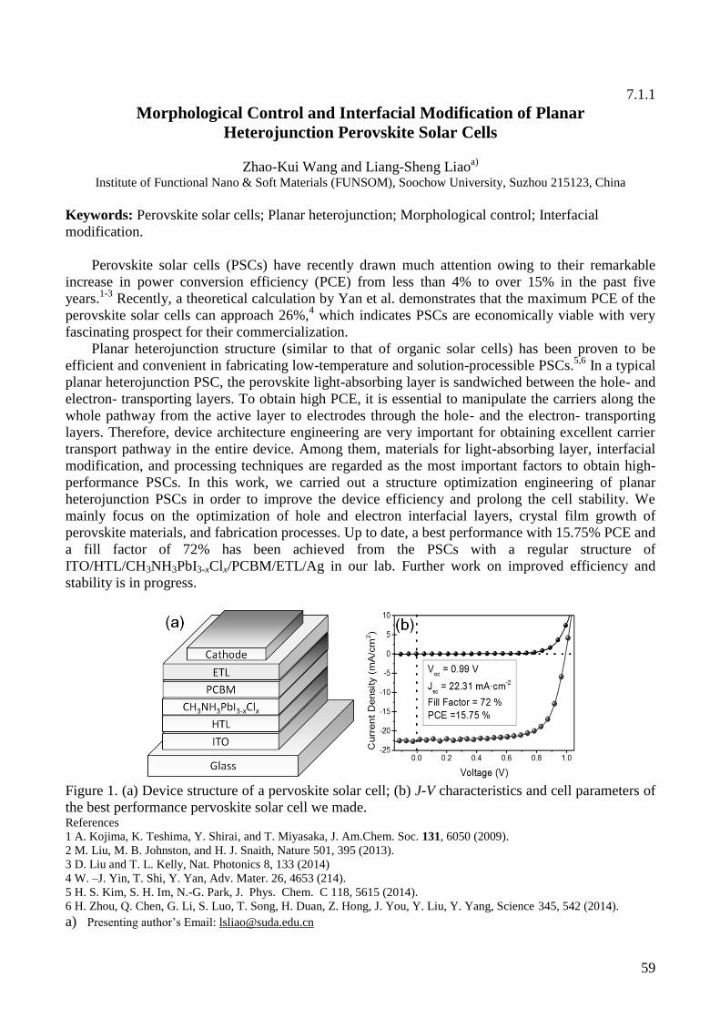
59
7.1.1
Morphological Control and Interfacial Modification of Planar
Heterojunction Perovskite Solar Cells
Zhao-Kui Wang and Liang-Sheng Liaoa)
Institute of Functional Nano & Soft Materials (FUNSOM), Soochow University, Suzhou 215123, China
Keywords: Perovskite solar cells; Planar heterojunction; Morphological control; Interfacial
modification.
Perovskite solar cells (PSCs) have recently drawn much attention owing to their remarkable
increase in power conversion efficiency (PCE) from less than 4% to over 15% in the past five
years.1-3
Recently, a theoretical calculation by Yan et al. demonstrates that the maximum PCE of the
perovskite solar cells can approach 26%,4 which indicates PSCs are economically viable with very
fascinating prospect for their commercialization.
Planar heterojunction structure (similar to that of organic solar cells) has been proven to be
efficient and convenient in fabricating low-temperature and solution-processible PSCs.5,6
In a typical
planar heterojunction PSC, the perovskite light-absorbing layer is sandwiched between the hole- and
electron- transporting layers. To obtain high PCE, it is essential to manipulate the carriers along the
whole pathway from the active layer to electrodes through the hole- and the electron- transporting
layers. Therefore, device architecture engineering are very important for obtaining excellent carrier
transport pathway in the entire device. Among them, materials for light-absorbing layer, interfacial
modification, and processing techniques are regarded as the most important factors to obtain high-
performance PSCs. In this work, we carried out a structure optimization engineering of planar
heterojunction PSCs in order to improve the device efficiency and prolong the cell stability. We
mainly focus on the optimization of hole and electron interfacial layers, crystal film growth of
perovskite materials, and fabrication processes. Up to date, a best performance with 15.75% PCE and
a fill factor of 72% has been achieved from the PSCs with a regular structure of
ITO/HTL/CH3NH3PbI3-xClx/PCBM/ETL/Ag in our lab. Further work on improved efficiency and
stability is in progress.
Figure 1. (a) Device structure of a pervoskite solar cell; (b) J-V characteristics and cell parameters of
the best performance pervoskite solar cell we made. References
1 A. Kojima, K. Teshima, Y. Shirai, and T. Miyasaka, J. Am.Chem. Soc. 131, 6050 (2009).
2 M. Liu, M. B. Johnston, and H. J. Snaith, Nature 501, 395 (2013).
3 D. Liu and T. L. Kelly, Nat. Photonics 8, 133 (2014)
4 W. –J. Yin, T. Shi, Y. Yan, Adv. Mater. 26, 4653 (214).
5 H. S. Kim, S. H. Im, N.-G. Park, J. Phys. Chem. C 118, 5615 (2014).
6 H. Zhou, Q. Chen, G. Li, S. Luo, T. Song, H. Duan, Z. Hong, J. You, Y. Liu, Y. Yang, Science 345, 542 (2014).
a) Presenting author’s Email: [email protected]

60
7.1.2
Optical Constants Measurements of Organometal Halide Perovskite Thin Films
and Their Application in the Solar Cell Structure Design
Hao-Wu Lin1,a),b)
1Department of Materials Science and Engineering, National Tsing Hua University,
No. 101, Section 2, Kuang-Fu Road, Hsinchu, Taiwan 30013.
Keywords: Organometal halide perovskites, Perovskite solar cells, Optical constants, Optical field
simulation, Tandem solar cells
We developed a new sequential layer-by-layer deposition method for fabricating organometal
halide perovskite thin films. The resulting films exhibit a homogenous morphology with a low root
mean squared roughness. The optical constants including refractive index and extinction coefficient
of organometal halide perovskites in the wavelength range of 300 to 1100 nm were determined.
These data were used for designing the optical structures of thin-film type perovskite solar cells. The
calculations suggest that power conversion efficiency of up to 20% and 29% are feasible without any
antireflection and light scattering structures in single and perovskite/CIGS tandem cells given a
proper device structure design. The calculation also indicates that even in optically optimised cells,
an average reflection of ~10% existed in both single and perovskite/CIGS tandem cells. A proper
integration of an antireflection optical structure to lower the reflection of the devices can most likely
further increase the device performance.

61
7.1.3
Formation chemistry of perovskite and photoconversion mechanism in
perovskite/fullerene heterojunctions
Tsz-Wai Nga)
, Ming-Fai Lo, Chun-Sing Lee
Center of Super-Diamond and Advanced Films (COSDAF), Department of Physics and Materials
Science, City University of Hong Kong, Hong Kong SAR, P. R. China
Keywords: Interface energetics, XPS, formation chemistry, methylammonium iodide, lead chloride
General studies believed that organometal halide perovskite form type II P-N junctions with
fullerene derivatives (C60 or PCBM), which provide sufficient driving force for exciton dissociation.
To the best of our knowledge, there is so far no experiment proof on this assumption. On the other
hand, whether photo-generated excitons in perovskites can intrinsically dissociate without any
assistance from a P-N junction is still controversial. Although perovskites have attracted much
attention in recent years, current understanding to perovskites such as formation chemistry and
photovoltaic behavior are indeed very limited.
To address these issues, we directly examine the formation chemistry and the surface
energetics of a vacuum-deposited perovskite/C60 and a solution-processed perovskite/PCBM
junctions via x-ray and ultraviolet photoelectron spectroscopic (XPS/UPS) studies. We showed with
evidence that the Cl would readily leave the Pb when lead chloride meets the methylammonium
iodide molecules such that negligible Cl could be observed in the resulting perovskite film. Also
contrary to the common believes, both junctions of perovskite/C60 and perovskite/PCBM are found
to be type I N-N junctions with bandgap of the perovskites embedded by that of the fullerene.
Meanwhile, device with such a charge inert junction can still effectively functions as a solar cell.
These results directly showed that excitons can dissociated to free carriers in the perovskite film even
without any assistance from a P-N junction.
a) [email protected] (T.W. Ng); [email protected] (C.S. Lee)
62
7.1.4
Interface engineering from Organic Solar cells to Perovskite Solar Cells via
Incorporation of a Polyelectrolyte Interlayer
Hong Zhang1,2,a),b)
, Jie Min1, Tayebeh Ameri
1, Ullrich Scherf
4, Christoph J. Brabec
1,3
1Institute of Materials for Electronics and Energy Technology (i-MEET), Friedrich-Alexander-University
Erlangen-Nuremberg, Martensstraße 7, 91058 Erlangen, Germany 2Erlangen Graduate School in Advanced Optical Technologies (SAOT), Paul-Gordan-Straße 6, 91052
Erlangen, Germany 3Bavarian Center for Applied Energy Research (ZAE Bayern), Haberstraße 2a, 91058 Erlangen, Germany 4Macromolecular Chemistry Group (buwmakro) and Institute for Polymer Technology (IfP), Bergische
Universität Wuppertal, Gaußstraße 20, 42119 Wuppertal, Germany
Keywords: interface engineering, organic solar cells, perovskite solar cells, polyelectrolyte
interlayer, solution processing.
The physical process involved in charge injection, extraction, transfer and recombination at an
electrode–semiconductor interface were found to be a most critical factor determining device
characteristics and stability. To minimize the contact barrier, the interface between the electrode and
the organic semiconductor layer should be a quasi-ohmic contact. Such a requirement has led to
efforts in interfacial engineering, including the use of thermally deposited LiF or bathocuproine
(BCP), self-assembled monolayers (SAMs), conjugated polyelectrolytes (CPEs) and polyelectrolytes
(PEs). The suitability of the interface opens the opportunity to apply the interface design rules for the
organic solar cell to the perovskite solar cell technology.
Regarding organic solar cells, we successfully demonstrate a smart strategy to use aluminum
doped ZnO (AZO) and the thiophene-based conjugated polyelectrolyte P3TMAHT as an interfacial
layer in small molecule solution-processed inverted solar cells (ITO / AZO / P3TMAHT / N(Ph-2T-
DCN-Et)3:PC71BM / MoO3 / Ag). Modification of AZO with a thin P3TMAHT layer increases the
photovoltaic properties of the inverted cell as a result of reduction in the work function of the
cathode with well aligned frontier orbital energy levels for efficient charge transport and reduced
surface recombination. The inverted device achieved 16% performance improvement dominantly by
recapturing part of the Voc losses when going from conventional to the inverted architecture.1
Apply the interface design rules for the organic solar cell to the perovskite solar cell technology.
Highly efficient hybrid organic/inorganic perovskite planar heterojunction (PHJ) solar cells (ITO /
PEDOT:PSS / CH3NH3PbI3-xClx / PCBM / polyelectrolyte interlayer /Ag) are fabricated based on
the interface layers all solution-processed at low temperature. Relative to the control device, the
power conversion efficiency (PCE) increased significantly from 8.53% for the control device to
12.01% (PEIE) and 11.28% (P3TMAHT) via incorporation of a polyelectrolyte interlayer. The
improvement in PCE for devices is chiefly assigned to the effective influence of polyelectrolyte
interlayers on reducing the work function of the subsequently deposited metal electrode, thereby
lowering the electron-injection barriers.2
References
(1) Min, J.; Zhang, H.; Stubhan, T.; Luponosov, Y. N.; Kraft, M.; Ponomarenko, S. A.; Ameri,
T.; Scherf, U.; Brabec, C. J. Journal of Materials Chemistry A 2013,1, 11306-11311.
(2) Zhang, H.; Azimi, H.; Hou, Y.; Ameri, T.; Przybilla, T.; Spiecker, E.; Kraft, M.; Scherf, U.;
Brabec, C. J. Chemistry of Materials 2014, 26 (18), 5190-5193.
a&b) Email: [email protected]

63
7.2.1
Monolithic integration of OLED and OPD for sensor application
Hoi Lam Tam1,a)
, Wing Hong Choi1, Xizu Wang
2, and Furong Zhu
1,b)
1Institute of Advance materials, Department of Physics, Hong Kong Baptist University
224 Waterloo Road, Kowloon Tong, Hong Kong 2Institute of Materials Research and Engineering, No. 3 Research Link Singapore, 117602
Keywords: Organic light emitting diode, Organic photodiode, Organic sensor
Organic electronics semiconductors are gradually revealing potential in photons generation,
transmission and detection, such as information and communication technology, bio-sensor and
computing. In this work, we propose proximity sensor device based on integration OLED and semi-
transparent OPD using simple top and bottom approach. Ag/CFx bilayer electrode is used to enable a
good electrical contact and work function matched electrodes in-between the OLED and OPD. The
Ag/CFx electrode also acts as a partial reflection mirror to enable the microcavity effect, such that it
enhances the forward emission at wavelength 522nm. We find that our design can exhibit high
luminance from the microcavity OLED (MOLED) and high respond from the OPD in the integrated
device. By changing the thickness of the active layer in the OPD, the signal contrast can be
enhanced. It is shown to exhibit the high coupling, based on their optical simulation. It suggests a
new way in which organic integrated devices have great potential in optocoupler, smart light source
and display, optical switches and smart organic optoelectronics device in organic optical
communication.

64
7.2.2
Improved Performance of Organic Solar Cells
by Incorporation of Coated Gold Nanorods at different positions
Yanxia Cui1, 2,a,b
, Haoyang Zhao1, Peiqian Tong
1,2, Qinjun Sun
1, Yuying Hao
1, Furong Zhu
1,2
1 Key Lab of Advanced Transducers and Intelligent Control System, Ministry of Education and
Shanxi Province, College of Physics and Optoelectronics, Taiyuan University of Technology,
Taiyuan 030024, China, 2 Hong Kong Baptist University, 224 Waterloo Road, Kowloon Tong, Hong
Kong
Keywords: Organic solar cells; Surface Plasmons; Gold nanorods; Coating; Absorption
Research on bulk heterojunction organic solar cells (BHJ-OSCs) has become one of the hottest
research topics due to their good performances, such as lightweight, flexible, inexpensive to
fabricate, and tunable on the molecular level [1, 2]. Recently, metallic nanoparticles (MNPs) with
different shape have been frequently used to improve the light trapping capability of OSC active
layer, hence increasing the power conversion efficiency (PCE) [3, 4]. The improved performance of
OSC devices can be ascribed to the excitation of surface plasmons or the enhancement of scattering.
As the synthesized MNPs are water-soluble, most of the present work have doped the MNPs into the
buffer layer of OSCs [5, 6]. Here, we present two different ways to introduce MNPs into
PTB7:PC70BM based OSCs for improving the device performances. The MNPs are the gold
nanorods, displaying two different resonant peaks for broadband enhancement of absorption. The
first way is to incorporate silica-coated gold nanorods at the interface between the active layer and
the buffer layer. The second way is to use NH2-PEG-SH to modify the surface of gold nanorods so
that the MNPs can be dissolved in DCB and hence to be easily mixed with the active blender. The
coating process is imported to avoid the quenching of excitons happening when the bare MNP
directly contact with the active material. Our experiments have shown that the introduction of coated
gold nanorods can greatly improve the device performance and the second way is superior, which
can bring as high as 10.5% improvement of PCE. Our research will contribute to the development of
high efficiency photovoltaic cells.
a) Presenting author’s Email: [email protected]
b) Corresponding author’s Email: [email protected], [email protected]
1. G. Dennler, M. C. Scharber, and C. J. Brabec, "Polymer-fullerene Bulk-heterojunction Solar Cells,"
Advanced Materials 21, 1323-1338 (2009).
2. Y. Liang, Z. Xu, J. Xia, S. Tsai, Y. Wu, G. Li, C. Ray, and L. Yu, "For the bright future-bulk
heterojunction polymer solar cells with power conversion efficiency of 7.4%," Advanced Materials 22,
E135-E138 (2010).
3. X. Li, W. C. H. Choy, H. Lu, W. E. I. Sha, and A. H. P. Ho, "Efficiency Enhancement of Organic Solar
Cells by Using Shape-dependent Broadband Plasmonic Absorption in Metallic Nanoparticles,"
Advanced Functional Materials 23, 2728-2735 (2013).
4. J.-L. Wu, F.-C. Chen, Y.-S. Hsiao, F.-C. Chien, P. Chen, C.-H. Kuo, M. H. Huang, and C.-S. Hsu,
"Surface plasmonic effects of metallic nanoparticles on the performance of polymer bulk heterojunction
solar cells," ACS nano 5, 959-967 (2011).
5. L. Lu, Z. Luo, T. Xu, and L. Yu, "Cooperative plasmonic effect of Ag and Au nanoparticles on
enhancing performance of polymer solar cells," Nano letters 13, 59-64 (2012).
6. A. Y. Mahmoud, J. Zhang, D. Ma, R. Izquierdo, and V.-V. Truong, "Optically-enhanced performance of
polymer solar cells with low concentration of gold nanorods in the anodic buffer layer," Organic
Electronics 13, 3102-3107 (2012).

65
7.2.3
Aggregation and morphology control enables multiple cases of >10% efficiency
polymer solar cells
He Yan
Department of Chemistry, The Hong Kong University of Science and Technology, Clear Water Bay,
Kowloon, Hong Kong.
Keywords: Polymer Solar Cell, Thick Film Polymer Solar Cell, Non-PCBM Solar Cell, Non-
fullerene Solar Cell
Although the field of polymer solar cell has seen much progress in device performance in the
past few years, several limitations are holding back its further development. For instance, current
high-efficiency (>9.0%) cells are restricted to material combinations that are based on limited donor
polymers and only one specific fullerene acceptor. Here we report the achievement of high-
performance (efficiencies up to 10.8%, fill factors up to 77%) thick-film polymer solar cells for
multiple polymer:fullerene combinations via the formation of a nearideal polymer:fullerene
morphology that contains highly crystalline yet reasonably small polymer domains. This morphology
is controlled by the temperature-dependent aggregation behaviour of the donor polymers and is
insensitive to the choice of fullerenes. The uncovered aggregation and design rules yield three high-
efficiency (>10%) donor polymers and will allow further synthetic advances and matching of both
the polymer and fullerene materials, potentially leading to significantly improved performance and
increased design flexibility.
A 6.3% Efficient Non-Fullerene Organic Solar Cells Enabled by a Properly
Matched Polymer Donor and Small-Molecular Acceptor
He Yan 1
Department of Chemistry, The Hong Kong University of Science and Technology, Clear Water
Bay, Kowloon, Hong Kong.
A high-performance non-fullerene acceptor based organic solar cells enabled by the combination
of a difluorobenzothiadizole donor polymer named PffBT4T-2DT and a small molecule named SF-
PDI2 was studied. It is found that SF-PDI2 matches particularly well with PffBT4T-2DT, and non-
fullerene organic solar cells with an impressive VOC of 0.98 V and a high power conversion
efficiency of 6.3% are achieved. Our study shows that PffBT4T-2DT is a promising donor material
for small-molecular acceptor-based organic solar cells and the selection of a matching small –
molecular acceptor is also important to achieve the best organic solar cell performance.
Representing and corresponding author: [email protected] Reference:
1. Liu, Y., Yan, H., etc “Aggregation and morphology control enables multiple cases of high-efficiency
polymer solar cells.” Nat. Commun., 5, 5293, (2014).
2. Liu, Y., Yan, H., etc “A tetraphenylethylene core-based 3D-structure small molecule acceptor enabling
efficient non-fullerene organic solar cells.” Adv. Mater., (2014), DOI: 10.1002/adma.201404152.
3. Zhao, Yan, H. etc, “High-Efficiency Non-Fullerene Organic Solar Cells Enabled by a
Difluorobenzothiadizole-Based Donor Polymer Combined with a Properly Matched Small Molecule
Acceptor.” Energy & Environmental Science., (2014), DOI:10.1039/C4EE02990A.
4. Mu, C., Yan, H., etc “High-Efficiency All-Polymer Solar Cells Based on a Pair of Crystalline Low-
Bandgap Polymers.” Adv. Mater., (2014), DOI: 10.1002/adma.201402473.
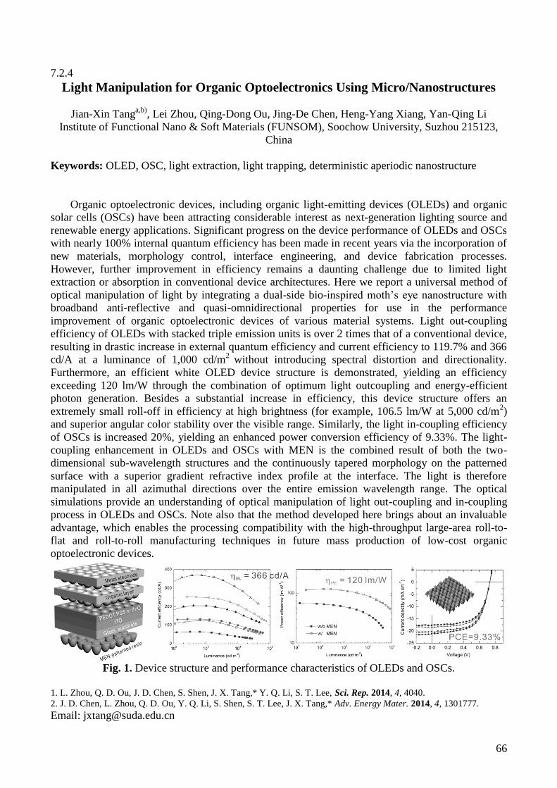
66
7.2.4
Light Manipulation for Organic Optoelectronics Using Micro/Nanostructures
Jian-Xin Tanga,b)
, Lei Zhou, Qing-Dong Ou, Jing-De Chen, Heng-Yang Xiang, Yan-Qing Li
Institute of Functional Nano & Soft Materials (FUNSOM), Soochow University, Suzhou 215123,
China
Keywords: OLED, OSC, light extraction, light trapping, deterministic aperiodic nanostructure
Organic optoelectronic devices, including organic light-emitting devices (OLEDs) and organic
solar cells (OSCs) have been attracting considerable interest as next-generation lighting source and
renewable energy applications. Significant progress on the device performance of OLEDs and OSCs
with nearly 100% internal quantum efficiency has been made in recent years via the incorporation of
new materials, morphology control, interface engineering, and device fabrication processes.
However, further improvement in efficiency remains a daunting challenge due to limited light
extraction or absorption in conventional device architectures. Here we report a universal method of
optical manipulation of light by integrating a dual-side bio-inspired moth’s eye nanostructure with
broadband anti-reflective and quasi-omnidirectional properties for use in the performance
improvement of organic optoelectronic devices of various material systems. Light out-coupling
efficiency of OLEDs with stacked triple emission units is over 2 times that of a conventional device,
resulting in drastic increase in external quantum efficiency and current efficiency to 119.7% and 366
cd/A at a luminance of 1,000 cd/m2
without introducing spectral distortion and directionality.
Furthermore, an efficient white OLED device structure is demonstrated, yielding an efficiency
exceeding 120 lm/W through the combination of optimum light outcoupling and energy-efficient
photon generation. Besides a substantial increase in efficiency, this device structure offers an
extremely small roll-off in efficiency at high brightness (for example, 106.5 lm/W at 5,000 cd/m2)
and superior angular color stability over the visible range. Similarly, the light in-coupling efficiency
of OSCs is increased 20%, yielding an enhanced power conversion efficiency of 9.33%. The light-
coupling enhancement in OLEDs and OSCs with MEN is the combined result of both the two-
dimensional sub-wavelength structures and the continuously tapered morphology on the patterned
surface with a superior gradient refractive index profile at the interface. The light is therefore
manipulated in all azimuthal directions over the entire emission wavelength range. The optical
simulations provide an understanding of optical manipulation of light out-coupling and in-coupling
process in OLEDs and OSCs. Note also that the method developed here brings about an invaluable
advantage, which enables the processing compatibility with the high-throughput large-area roll-to-
flat and roll-to-roll manufacturing techniques in future mass production of low-cost organic
optoelectronic devices.
Fig. 1. Device structure and performance characteristics of OLEDs and OSCs.
1. L. Zhou, Q. D. Ou, J. D. Chen, S. Shen, J. X. Tang,* Y. Q. Li, S. T. Lee, Sci. Rep. 2014, 4, 4040.
2. J. D. Chen, L. Zhou, Q. D. Ou, Y. Q. Li, S. Shen, S. T. Lee, J. X. Tang,* Adv. Energy Mater. 2014, 4, 1301777.
Email: [email protected]

67
8.1.1
Effect of film drying condition on performance of polymer solar cells for
bis-PCBM/P3HT
Masaru Nagai1,a)
, Huang Wei1, Yuji Yoshida
2
1 Key Laboratory of Flexible Electronics (KLOFE) & Institute of Advanced Materials (IAM),
Jiangsu National Synergistic Innovation Center for Advanced Materials (SICAM), Nanjing Tech
University (NanjingTech), 30 South Puzhu Road, Nanjing 211816, P.R. China
2 National Institute of Advanced Industrial Science and Technology (AIST), Research
Center for photovoltaic technology, Higashi 1-1-1, Tsukuba, Ibaraki 305-5565, Japan [email protected]
Keywords: polymer solar cell, bulk-heterojunction, slow dry, bis-PCBM
Polymer solar cells (PSC) have been actively studied as a major candidate for the next-
generation of solar cells. The performance of PSCs is affected by the device fabrication condition
and various techniques have been proposed, including thermal annealing and solvent annealing
methods. A similar method to solvent annealing, the “slow drying method” has been proposed as
well [1]. It improves short circuit current density (Jsc) by delaying the drying speed of the coated
films. However, compared with the first two methods, less research has been reported about slow
drying and it is not commonly used as a fabrication method for PSC. In this study, the slow drying
method was applied to PSCs consisting of p-type polymers poly(3-hexylthiophene) (P3HT) and n-
type fullerene derivative bis-[6,6]-phenyl-C61-butyric acid methyl ester (PCBM), and the effect of
drying speed on the cell performance and the method’s mechanism were investigated. The prepared
devices had a structure, glass/indium tin oxide (ITO) anode/poly(3,4-
ethylenedioxythiophene)/poly(styrenesulfonate) (PEDOT/PSS)/bis-PCBM:P3HT (1:1)/Al cathode.
The active layers were formed using doctor blade method. The film drying speed was controlled by
varying the partial pressure of the solvent used (chlorobenzene). After Al cathodes were formed,
thermal annealing 150 ºC, 15 min. was performed using a hot plate. The performance of each (22
mm) cell was estimated under AM 1.5 solar simulated illumination. Figure 1 denotes the relation
between the cell performance and film drying time. Note that the drying time denotes the period
from the solution drop to the timing of phase separation process had been completed. The PSC
formed by conventional spin
casting method evinced very poor
performance, Jsc=5.85 mA/cm2,
Voc=0.69 V, FF=0.21,
PCE=0.83%. In contrast, Jsc of the
devices with slow drying clearly
increased. The Jsc increased to 7.02
mA/cm2
by setting t at 60 seconds
and exceeded 8 mA/cm2
by
expanding t to 700 seconds. By
optimizing the cathode buffer
layers and thermal annealing
condition, we attained high
performance of 4.05% PCE for this
system.
[1] Mihailetchi, et.al. Appl. Phys.
Lett. 89, 012107 (2006)
Fig. 1 Performance of polymer solar cells and drying
time
b
68
8.1.2
Efficiency enhancement in inverted organic solar cells using a dual cathode
interlayer
Bo Wu 1,a)
, Zhenghui Wu 1)
, Tam Hoi Lam 1)
, Furong Zhu 1,b)
, Tsz-Wai Ng 2)
and Chun-Sing Lee 2)
1Department of Physics and Institute of Advanced Materials, Hong Kong Baptist University,
Kowloon Tong, Hong Kong 2List Center of Super-Diamond and Advanced Films (COSDAF), Department of Physics and
Materials Science, City University of Hong Kong, Kowloon Tong, Hong Kong
Keywords: organic solar cell, cathode interlayer, charge collection, inverted structure.
Organic solar cells (OSCs) with inverted structure exhibit higher power conversion efficiency
(PCE) and are more stable than similar devices with regular configuration. Although indium tin
oxide (ITO) is normally used as an anode, it can also act as a transparent cathode when the surface is
modified to lower its work function with an interlayer, such as ZnO or TiO2, to promote more
efficient electron collection. In this work, the effect of a dual cathode interlayer of Al (~1.2 nm)/ZnO
on PCE of inverted OSCs based on PTB7:PC70BM system is analyzed. The results reveal that the use
of Al (~1.2 nm)/ZnO-modified ITO cathode allows achieving a PCE of 7.2% which is 20% higher
than that of a structurally identical control cell made with just a ZnO/ITO cathode. Light intensity-
dependent current densityvoltage characteristics point out the enhancement of charge collection
efficiency due to the presence of Al (~1.2 nm)/ZnO interlayer at the organic/electrode interface. X-
ray Photoelectron Spectroscopy (XPS) analysis indicates clearly that the thermally prepared Al layer
on ZnO was indeed partially oxidized and should be considered as AlOx. Ultraviolet photoelectron
spectroscopy measurements fully reveal the energy level alignment at the interface between AlOx
and PC70BM, which show a removal of the energy level pinning at ZnO/PC70BM interface, leading
to less bimolecular carrier recombination and leakage current. Moreover, improved repeatability on
the performance of devices is also achieved with this dual cathode interlayer. All the results and
analyses above confirm that the surface modification of ITO cathode with an AlOx (~1.2 nm)/ZnO
interlayer is an effective approach for the realization of inverted OSCs with high efficiency and
stability.

69
8.1.3
Printing Fabrication and Interface Materials for
Solution-Processed Organic Photovoltaics
Junliang Yang, ab*
Jian Xiong, ab
Qiao Hu, ab
Yongli Gao abc
a Institute of Super-microstructure and Ultrafast Process in Advanced Materials, School of Physics
and Electronics, Central South University, Changsha, Hunan 410083, China b
Hunan Key Laboratory for Super-microstructure and Ultrafast Process, School of Physics and
Electronics, Central South University, Changsha, Hunan 410083, China c Department of Physics and Astronomy, University of Rochester, Rochester, NY 14627, USA
Keywords: organic photovoltaics; R2R printing; interface; module
Organic photovoltaics (OPVs) continuously attract attention due to their potential as low cost
and lightweight sources of renewable energy. The power conversion efficiency (PCE) of state-of-the-
art OPVs, based on bulk heterojuction and tandem structures, can reach over 10.0 %, as result of
progress in new materials, device engineering, device physics, etc. [1]. Especially, there has been an
unexpected breakthrough and rapid evolution of highly efficient solar cells based on organic-
inorganic hybrid perovskite materials [2]. However large-area OPVs processed by R2R printing or
coating techniques still have many issues, and the PCE of large-area OPV modules is much lower
than those of smaller, spin-coated devices [3, 4]. In this presentation, we will describe our research
on the fabrication of OPV modules by R2R printing techniques and the solution stability of active
materials, as well as the solution-processed interface materials for printed OPVs [4-7]. It is very
important to optimize printing parameters, ink properties, and interface materials for obtaining high-
quality printed thin films and printed OPV modules.
Fig.1 Self-developed R2R multi-function printer/coater
and its application in the fabrication of organic solar cells
Acknowledgements
This work was supported by National Natural Science Foundation of China (51203192), Hunan Provincial Natural
Science Foundation for Distinguished Young Scholars (2015JJ1015), and the Program for New Century Excellent
Talents in University (NCET-13-0598),
References
[1] M. A. Green, K. Emery, Y. Hishikawa, et. al., Prog. Photovolt: Res. Appl., 20 (2012), 12.
[2] J. Burschka, N. Pellet1, S. J. Moon, et. al., Nature, 499 (2013) 316; M. Liu, M. B. Johnston, H. J. Snaith, Nature, 501
(2013) 395; H. P. Zhou, Q. Chen, G. Li, et. al., Science, 345 (2014), 542; A. Y. Mei, X. Li, L. F. Liu, et.al., Science,
345 (2014), 295.
[3] F. C. Krebs, T. Tromholt, M. Jørgensen, Nanoscale, 2 (2010), 873–886.
[4] J. L. Yang, D. Vak, N. Clark, et. al., Sol. Energy Mater. Sol. Cells, 109 (2013), 47.
[5] J. Xiong, J. L. Yang, B. C Yang, et. al., Org. Electron., 15 (2014), 1745.
[6] J. Xiong, B. C. Yang, C. H. Zhou, J. L. Yang, et. al., Org. Electron., 15 (2014), 835.
Email: [email protected] (J. L. Yang); +86-731-88660256
70
8.1.4
Interface Engineering and Morphology Control for High Performance
Perovskite/Fullerene Planar Heterojunction Solar Cells
Hin-Lap Yipa)
, Qifan Xue, Chen Sun, Zhicheng Hu, Fei Huang, Yong Cao
State Key Laboratory of Luminescent Materials and Device, South China University of Technology,
Guangzhou, China
Keywords: planar heterojunction, perovskite solar cells, interface engineering, morphology control
Solar cells based on organometal trihalide perovskites (eg. CH3NH3PbI3) as light absorbers
are emerging as a low-cost and high performance photovoltaic technology that may fulfil the
requirement for large-scale deployment of solar energy. Over the past few years, significant progress
was made in pervoskite solar cells with power conversion efficiencies (PCE) shot up from 3% to
18%. Recent studies revealed that organometal trihalide pervoskites exhibit several desired properties
for photovoltaic applications including facile tunable bandgaps, high absorption coefficient, long
carrier-diffusion lengths, high ambipolar mobilities and low exciton binding energy, making them a
very appealing class of material for new generation photovoltaic technology.
In this talk we will present two strategies to improve the performance of perovskite/fullerene
planar heterojunction solar cells.1 First, the growth kinetic of the perovskite films was tuned by
introducing chemically-tailored processing additives. Depending on the choice of the additives, the
crystallinity and coverage of the perovskite films can either be enhanced or suppressed and we found
that the solar cell performance was strongly depending on the morphology of the perovskite films.2
Second, novel interfacial materials were introduced to improve the contact between the fullerene
electron transport layer and the metal cathode interface, resulted in Ohmic contact with reduced
interfacial resistance and a significant improvement on the fill factor. Combining these two strategies
high performance perovskite solar cells with over 15% PCE were achieved.3
Reference: 1. Q. Xue, C. Sun, Z. Hu, F. Huang, H.-L. Yip, Y. Cao, Acta Chim. Sinica, 2014, DOI:10.6023/A14090674
2. Q. Xue, Z. Hu, C. Sun, Z. Chen, F. Huang, H.-L. Yip and Y. Cao, RSC Adv., 2014, DOI: 10.1039/C4RA11739E
3. Q. Xue, Z. Hu, J. Liu, J. Lin, C. Sun, Z. Chen, C. Duan, J. Wang, C. Liao, W. M. Lau, F. Huang, H.-L. Yip, Y.
Cao, J. Mater. Chem. A, 2014, 2, 19598
a) Presenting and corresponding author’s email: [email protected]
71
8.1.5
Improved organic photovoltaics by surface plasmon effect
Yuying Hao
1 b),Yanxia Cui1, 2 a),Ye zhang
1,Wenyan Wang1, Ximin Tian
1,Yang Hao1,Furong Zhu
2
1 Key Lab of Advanced Transducers and Intelligent Control System of Ministry of Education,
College of Physics and Optoelectronics, Taiyuan University of Technology, Taiyuan 030024,
China 2Hong Kong Baptist University, 224 Waterloo Road, Kowloon Tong, Hong Kong
Keywords: Organic photovoltaics, surface plasmon effect, nanograting, metal nanoparticles
Organic photovoltaics (OPVs) have great potential as a clean and renewable energy source technology due
to their wide material sources, relatively low-cost, light weight, transparency as well as their compatibility
with large area flexible substrates. However, the energy conversion efficiencies are less satisfactory at present
compared with their inorganic counterparts. In OPV devices, very thin active layers are necessary due to some
intrinsic properties of organic materials, such as low carrier mobility and short exciton diffusion length.
However, the incident photons could not be absorbed sufficiently in such thin active layers. This
incompatibility is one of the main reasons for the low energy conversion efficiency of OPV devices.
Therefore, it is necessary to find ways to enhance light absorption effectively in the active layer without
increasing its thickness. Different approaches have been reported including incorporating metal nanoparticles
(NPs) and periodic surface plasmon structures in OPV devices to boost light absorption. In this talk, we will
report some theoretical and experimental investigations on improving the energy conversion efficiency using
the surface plasmon effect in our labs: In theory, novel 1D metal nanogratings were designed for achieving
high-efficiency, broad-band and wide-angle optical absorption in OPVs; In experiment, the coated metal
nanoparticles were incorporated in OPVs for improving the energy conversion efficiencies.
Reference
[1] W. Wang, Y. Hao, Y. Cui, X. Tian, Y. Zhang, H. Wang, F. Shi, B. Wei, and W. Huang, Opt. Express 22,
A376-A385 (2014).
[2] X. Tian, W. Wang, Y. Hao, Y. Lin, Y. Cui, Y. Zhang, H. Wang, B. Wei, and B. Xu, J. Mod. Opt. doi
10.1080/09500340.2013.879218, 2014
[3] X. Tian, Y. Hao, Y. Zhang, Y. Cui, T. Ji, H. Wang, B. Wei and W. Huang, Opt. Commun., 338( 1), 226-
232 (2015)
[4]Y. Hao, J. Song, F. Yang, Y. Hao, Q. Sun, J. Guo, Y. Cui, H. Wang and F. Zhu, J. Mater. Chem. C
(Accepted)
[5] W. Wang, Y. Cui, Y. He, Y. Hao, Y. Lin, X. Tian, T. Ji, and S. He, Opt. Lett. 39(2), 331-334 (2014).
[6] Z. Li, Z. Qiao, W. Liu, Z. Wang, H. Wang, F. Shi, Y. Hao, Mater. Lett., 139 (15), 307-310 (2015)
[7] Y. Cui, Y. He, Y. Jin, F. Ding , Y. Ye, S. Zhong, Y. Lin, S. He, Laser & Photonics Reviews, 8(4), 495-520
(2014)
a) Presenting author’s Email: [email protected]
b) Corresponding author’s Email: [email protected]

72
8.2.1
Contrary interfacial exciton dissociation at metal/organic interface in regular and
inverted organic solar cells
Bo Wu, Zhenghui Wu, Qingyi Yang, Hanxiao Liu, Hoi Lam Tam Furong Zhu a)
Department of Physics and Institute of Advanced Materials, Hong Kong Baptist University,
Kowloon Tong, Hong Kong
Keywords: organic solar cells, transient photocurrent, metal/organic interface
An investigation of the absorption enhancement and stability of organic solar cells (OSCs) with
regular and reverse configurations has been performed. Light absorption in the regular and reverse
geometry OSCs was calculated using finite-difference time-domaain simulations over the
wavelength range from 400 nm to 800 nm. The simulation reveals that OSCs with reverse geometry
possess a higher absorption compared to the structurally identical regular configuration OSCs
fabricated using an ITO/PEDOT:PSS anode. The reverse configuration OSCs, have an organic
functional stack sandwiched between an Al-modified ITO transparent cathode and an opaque bi-
layer MoO3/Ag anode is more efficient than a control regular OSC. The dissociation of excitons at
the Al/organic cathode interface in regular geometry OSCs hampers the electron collection. During
the deposition of Al contact on the stack of functional organic layers, the energetic metal atoms can
induce interfacial defects in the underlying functional organic layers, resulting in forming an adverse
charge collection behavior at the complex organic/Al interface. The origin of unfavorable electron
collection is mainly due to the compensation of drifted photo-generated electrons at the
organic/cathode (Al) interface, which can be eliminated, e.g., by inserting a thin ZnO interlayer
between the organic layer and Al electrode. This work clearly reveals that the removal of the
unfavorable interfacial exciton dissociation is a perquisite for a significant enhancement in power
conversion efficiency in OSCs.
73
8.2.2
Photovoltage Loss in Excitonic Solar cells
Sai-Wing Tsang
Department of Physics and Materials Science, City University of Hong Kong, Hong Kong
Keywords: Organic solar cell, photovoltaic, energy level, charge transfer state, open circuit voltage.
Polymer solar cells with power conversion efficiencies (PCEs) over 8% have been demonstrated in
laboratories with advances of novel materials, device processing, and device architectures. However,
some critical physical properties of the polymer:fullerene bulk heterojunctions (BHJs) such as the
donor-acceptor interface energetics which controls the charge transfer process are not well
understood. In a BHJ photovoltaic cell, the open-circuit voltage (VOC) is determined by the energy
level difference of the highest-occupied-molecular-orbital (HOMO) of the donor and the lowest-
unoccupied-molecular orbital (LUMO) of the acceptor. However, there is lack of experimental
approach to directly probe such alignment in a working device.
In this presentation, we will demonstrate a technique—charge modulated electroabsorption
spectroscopy (CMEAS) to directly determine the effective bandgap and the interface effective force
in a polymer:fullerene BHJ system.[1,2] By measuring the electroabsorption (EA) signal due to
charge-modulation (CM) in the polymer, we are able to observe a clear sub-bandgap signal through
direct excitation of excitons to the charge transfer states. Such a differential spectrum measured by
CMEAS has a much higher signal-to-noise ratio than that measured by linear optical absorption
techniques. Compared to the conventional electrochemical method, CMEAS can probe the energy
level alignment at the electron donor-acceptor interface in a working BHJ photovoltaic cell. Using
CMEAS, for the first time we are able to directly probe the effective bandgap in polymer:fullerene
systems. The results also bring insight into the details of the charge transfer states and the origin of
VOC in polymer photovoltaic cells.
[1] S.-W. Tsang, S. Chen, and F. So, Adv. Mater. 25, 2434 (2013)
[2] S. Chen, S.-W. Tsang, T.-H. Lai, J. R. Reynolds, and F. So, Adv. Mater. 26,61125 (2014)
74
8.2.3
High-efficiency all-polymer solar cells based
on a pair of crystalline low-bandgap polymers Cheng Mu
1, Peng Liu
2, Wei Ma*
,3, Kui Jiang
1, Jingbo Zhao
1, Kai Zhang
2, Zhihua Chen
4, Zhanhua
Wei1, Ya Yi
5, Jiannong Wang
5, Shihe Yang
1, Fei Huang*
, 2, Antonio Facchetti
4, Harald Ade*
, 3, He
Yan*, 1
1. Department of Chemistry, Hong Kong University of Science and Technology, Clear Water Bay,
KowLoon, Hong Kong.
2. Institute of Optoelectronic Materials and Devices, State Key Laboratory of Luminescent Materials
and Devices, South China University of Technology Guangzhou 510640, P. R. China.
3. Department of Physics, North Carolina State University, Raleigh, NC 27695, USA.
4. Polyera Corporation, 8045 Lamon Avenue, Skokie, Illinois 60077, USA.
5. Department of Physics, Hong Kong University of Science and Technology, Clear Water Bay,
KowLoon, Hong Kong.
Abstract
We have demonstrated high-performance all polymer solar cells (all-PSCs) based on a pair of
crystalline low-bandgap polymers. A high Jsc of 11.5 mA/cm2 and a PCE of 5% were achieved due
to the low optical bandgap of the donor polymer and the reasonably high EQE of the cell that is the
result of the favorable morphology of the NT:N2200 blends. R-SoXS, AFM and TEM
characterizations support that the NT:N2200 blend film is smooth and exhibits an average domain
size of about 100 nm. GIWAXS and charge transport data combined indicate that NT can maintain
its crystallinity with a preferrential face-on orientation in the NT:N2200 blends, which lead to a hole
mobility that is reasonably balanced with the electron mobility of N2200. Our morphological
characterizations can largely explain the performance of NT:N2200-based all-PSCs. Our results
provide important inspirations to develop high-efficiency all-PSCs based on donor polymers with
low optical bandgaps.
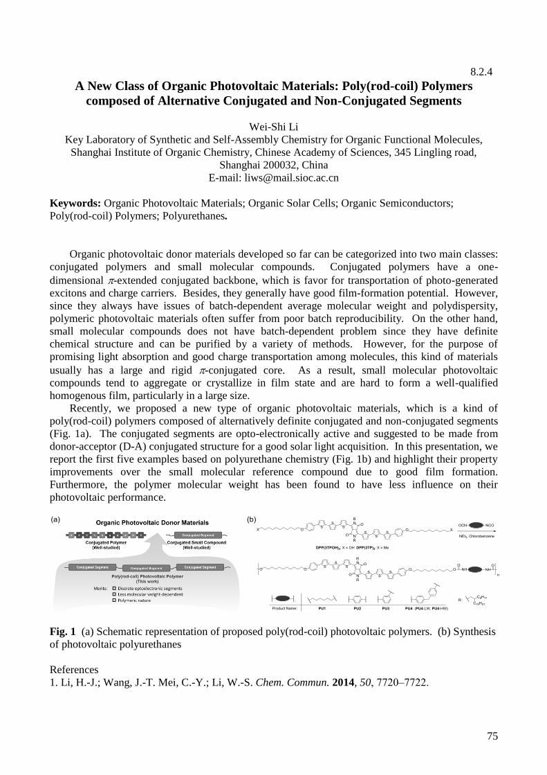
75
8.2.4
A New Class of Organic Photovoltaic Materials: Poly(rod-coil) Polymers
composed of Alternative Conjugated and Non-Conjugated Segments
Wei-Shi Li
Key Laboratory of Synthetic and Self-Assembly Chemistry for Organic Functional Molecules,
Shanghai Institute of Organic Chemistry, Chinese Academy of Sciences, 345 Lingling road,
Shanghai 200032, China
E-mail: [email protected]
Keywords: Organic Photovoltaic Materials; Organic Solar Cells; Organic Semiconductors;
Poly(rod-coil) Polymers; Polyurethanes.
Organic photovoltaic donor materials developed so far can be categorized into two main classes:
conjugated polymers and small molecular compounds. Conjugated polymers have a one-
dimensional -extended conjugated backbone, which is favor for transportation of photo-generated
excitons and charge carriers. Besides, they generally have good film-formation potential. However,
since they always have issues of batch-dependent average molecular weight and polydispersity,
polymeric photovoltaic materials often suffer from poor batch reproducibility. On the other hand,
small molecular compounds does not have batch-dependent problem since they have definite
chemical structure and can be purified by a variety of methods. However, for the purpose of
promising light absorption and good charge transportation among molecules, this kind of materials
usually has a large and rigid -conjugated core. As a result, small molecular photovoltaic
compounds tend to aggregate or crystallize in film state and are hard to form a well-qualified
homogenous film, particularly in a large size.
Recently, we proposed a new type of organic photovoltaic materials, which is a kind of
poly(rod-coil) polymers composed of alternatively definite conjugated and non-conjugated segments
(Fig. 1a). The conjugated segments are opto-electronically active and suggested to be made from
donor-acceptor (D-A) conjugated structure for a good solar light acquisition. In this presentation, we
report the first five examples based on polyurethane chemistry (Fig. 1b) and highlight their property
improvements over the small molecular reference compound due to good film formation.
Furthermore, the polymer molecular weight has been found to have less influence on their
photovoltaic performance.
Fig. 1 (a) Schematic representation of proposed poly(rod-coil) photovoltaic polymers. (b) Synthesis
of photovoltaic polyurethanes
References
1. Li, H.-J.; Wang, J.-T. Mei, C.-Y.; Li, W.-S. Chem. Commun. 2014, 50, 7720‒7722.

76
9.1
Efficiency and Reliability of Small Molecule Organic Photovoltaics
Stephen Forrest(a,b)
Departments of Electrical Engineering and Computer Science, Physics and Materials Science and
Engineering
University of Michigan
Ann Arbor, MI 48109 USA
Keywords: OPVs, Operational Lifetimes, Device/Material Properties
The viability of any photovoltaic technology rests on meeting three challenges that ultimately
impact cost/Watt: (i) Efficiency, (ii) Reliability and (iii) Low cost manufacturability. Organic
photovoltaics (OPVs) are attractive due to confidence that the third challenge can be met using low
energy, roll-to-roll processing using low cost and environmentally friendly materials. In this talk,
therefore, we will concentrate our attention on the recent and very rapid progress in meeting the
goals of high efficiency and long-term reliability. We will show work in our laboratory that has
resulted in demonstration of multijunction cells with efficiencies >11%, with every indication that
soon even higher efficiencies will be achieved. Furthermore, we will examine the fundamental
processes leading to device failure, and assess the potential for achieving cells with operational
lifetimes >20 years. The talk will consider all of these advances in the context of the physical limits
that can be expected based on fundamental considerations of device and materials properties.
77
9.2
Structural details and measurements related to organic nanodevice by STM
Li-Jun Wan
Institute of Chemistry, Chinese Academy of Sciences, Beijing 100190, China
E-mail: [email protected]
Abstract
Preparing hybrid or multi-component molecular architectures on solid surface is an important
issue in surface molecular science and molecular device fabrication. On the other hand, the questions
are always attracted our attention such as (1) what state is it when a molecule stays at a solid surface?
(2) how is the interfacial structure when a multilayer was formed? (3) how is the molecular behavior
when a multilayer was suffered to such as heat treatment? (4) how to measure the electronic property
of a single or monolayer? In this report, I will show you the results on the fabrication and property of
functional molecular assembly by using Alq3, BH-PPV and other donor/acceptor molecules. Since
Joule heating effect on electroluminescent efficiency will influence on OLED and other organic
nanodevice and result in the degradation of a device, thermal annealing on host-guest complex film
was employed to simulate Joule heating effect. STM and photoluminescence measurements were
performed on the guest molecule BT, host molecule TPBI, and their mixture deposited on HOPG
surface to study the degradation mechanism from thermal heating. The results show that by careful
designing of intermolecular and molecule/substrate reaction, various spontaneous and controllable
molecular assemblies can be fabricated on solid surface, which are promising candidates for organic
molecular nanodevice.
References:
1. L. Wang, L.J. Wan et al., J. Am. Chem. Soc., 2008, 130(40), 13433-13441.
2. J.R. Gong, L.J. Wan et al., J. Am. Chem. Soc., 2006, 128(38), 12384-12385.
3. J.R. Gong, L.J. Wan et al., J. Phys. Chem. B, 2005, 109, 1675-1682.

78
10.1
Interface effects in organic photovoltaics
Qinye Bao1,a)
, Oskar Sandberg,2 Daniel Dagnelund,
1 Simon Sandén,
2 Feng Gao,
1 Slawomir Braun,
1
Harri Aarnio,2 Xianjie Liu,
1 Weimin M. Chen,
1 Ronald Österbacka
2 and Mats Fahlman
1,b)
1Department of Physics, Chemistry and Biology, Linköping University, SE-58183 Linköping,
Sweden 2Center for Functional Materials, Department for Natural Sciences, Åbo Akademi University, FI-
20500 Turku, Finland
Keywords: Organic Photovoltaics, charge transfer states, doping, recombination, UPS
Organic photovoltaic is under intense development and significant focus has been placed on
tuning the donor ionization potential and acceptor electron affinity to optimize open circuit voltage.
Here we show that for a series of regioregular-poly(3-hexylthiophene):fullerene bulk heterojunction
organic photovoltaic devices with pinned electrodes, integer charge transfer states [1] present in the
dark and created as a consequence of Fermi level equilibrium at BHJ have a profound effect on open
circuit voltage. The integer charge transfer state formation causes vacuum level misalignment that
yields a roughly constant effective donor ionization potential to acceptor electron affinity energy
difference at the donor-acceptor interface, even though there is a large variation in electron affinity
for the fullerene series. The large variation in open circuit voltage for the corresponding device series
instead is found to be a consequence of trap-assisted recombination via integer charge transfer states.
Based on the results, novel design rules for optimizing open circuit voltage and performance of
organic bulk heterojunction solar cells are proposed [2].
The use of molecule-doped organic semiconductor layers in organic photovoltaics is showing
great promise [3] and the energy level alignment at molecule-doped conjugated polymer/electrode
interface is thus a topic of interest. We here study the energy level alignment of two molecule-doped
systems, rr-P3HT and TQ1, using F4TCNQ as the dopant. We find regular plots with a constant
thickness-independent displacement away from the original energy level alignment behavior of the
pristine polymer at low to intermediate level for molecule-doped conjugated polymer/conducting
substrate interfaces. We proposed that two combined processes control the energy level alignment:
(i) equilibration of the Fermi level due to oxidation (or reduction) of polymer sites at the interface as
per the integer charge transfer model and (ii) a double dipole step induced by image charge from the
dopant-polymer charge transfer complex that cause a shift of the work function. Such behavior is
expected to hold in general for low to intermediate level doped organic semiconductor systems.
[1] Slawomir Braun, et al, Adv. Mater. 21 (2009) 1450
[2] Qinye Bao, et al, Adv. Funct. Mater. 24 (2014) 6309
[3] www.heliatek.com
[4] Qinye Bao, et al, Adv. Mater. Interfaces, DOI: 10.1002/admi.201400403

79
10.2
Photocatalytic Reduction of Protons to Hydrogen
Chen-Ho Tung*, Li-Zhu Wu, Bin Chen, Zhi-Jun Li
Key Laboratory of Photochemical Conversion and Optoelectronic Materials, Technical Institute of
Physics and Chemistry, the Chinese Academy of Sciences, Beijing 100190, P. R. China
Keywords: Photocatalytic splitting of water, Quantum dot, [FeFe] hydrogenase, Transition metal
cluster.
One of the best solutions for meeting future energy demands is the conversion of water into
hydrogen fuel using solar energy. The splitting of water into molecular hydrogen (H2) and oxygen
(O2) using light involves two half-reactions: the oxidation of water to O2 and the reduction of protons
to H2. To take advantage of the full range of the solar spectrum, researchers have extensively
investigated artificial photosynthesis systems consisting of two photosensitizers and two catalysts
with a Z-configuration: one photosensitizer-catalyst pair for H2 evolution and the other for O2
evolution. This report reviews advances our laboratory has made in the development of new systems
for photocatalytic H2 evolution that uses earth-abundant materials and is both efficient and durable.
We constructed several assemblies of CdTe and CdSe QDs as photosensitizers with [FeFe]-H2ase
mimics as catalysts. These assemblies produced H2 in aqueous solutions photocatalytically and
efficiently, with turnover numbers (TONs) up to tens of thousands. Assemblies of 3-
mercaptopropionic acid (MPA)-capped CdTe Qds with Co2+
ions formed Coh-CdTe hollow
nanospheres, and (MPA)-capped-CdSe Qds with Ni+ ions produced Nih-CdSe/CdS core/shell hybrid
in situ in aqueous solutions upon irradiation. The resulting photocatalytic systems proved robust for
H2 evolution. These systems showed excellent activity and impressive durability in the
photocatalytic reaction, suggesting that they can serve as a valuable part of an overall water splitting
system.
References
[1]. Wu, L.-Z.; Chen, B.; Li, Z.-J.; Tung, C.-H. Acc. Chem. Res. 2014, 47, 2177-2185.
[2]. Wang, F.; Wang, W.-G.; Wang, X.-J.; Wang, H.-Y.; Tung, C.-H.; Wu, L.-Z. Angew. Chem.
Int. Ed. 2011, 50, 3193-3197.
[3]. Wang, F.; Liang, W.-J.; Jian, J.-X.; Li, C.-B.; Chen, B.; Tung, C.-H.; Wu, L.-Z. Angew. Chem.
Int. Ed. 2013, 52, 8134-8138.
[4]. Jian, J.-X.; Liu, Q.; Li, Z.-J.; Wang, F.; Li, X.-B.; Li, C.-B.; Liu, B.; Meng, Q.-Y.; Chen, B.;
Feng, K.; Tung, C.-H.; Wu, L.-Z. Nature Commun 2013, 4, 2695.
[5]. Li, Z.-J.; Wang, J.-J.; Li, X.-B.; Fan, X.-B.; Meng, Q.-Y.; Feng, K.; Chen, B.; Tung, C.-H.;
Wu, L.-Z. Adv. Mater. 2013, 25, 6613-6618.
[6]. Li, Z.-J.; Fan, X.-B.; Li, X.-B.; Li, J.-X.; Ye C.; Wang, J.-J.; Yu S.; Li, C.-B.; Gao, Y.-J.;
Meng, Q.-Y.; Tung C.-H.; Wu, L.-Z. J. Am. Chem. Soc. 2014, 136, 8261-8268.

80
10.3
Origin and control of gap states: A striking mobility improvement of C60 OFET
Jin-Peng Yang1,a)
, Fabio Bussolotti1, Alexander Hinderhofer
1,2, Satoshi Kera
1,3, and Nobuo Ueno
1,b)
1Graduate School of Advanced Integration Science, Chiba University, Inage-ku, Chiba 263-8522, Japan
2Institut fur Angewandte Physik, Universität Tubingen, Auf der Morgenstelle 10, Tubingen 72076, Germany
3Institute for Molecular Science, Myodaiji, Okazaki 444-8585, Japan
Keywords: gap states, energy level alignment, mobility, pentacene, C60
Charge carrier transport, which is central to the performance of various organic-based devices, is
strongly affected by localized electronic gap states originating from various polarons, structural
defects, impurities and/or chemical interactions with the gaseous environment. Detailed
investigations of gap states energy distribution are therefore of paramount importance to understand
the energy level alignment at interfaces and the intrinsic limits of transport in organic
semiconductors [1,2]. We use ultrahigh-sensitivity ultraviolet photoelectron spectroscopy (UPS) to
demonstrate that even exposure to seemingly innocuous inert gases such as N2 and Ar can have a
significant impact on the electronic properties of pentacene films [1.3], while F16Cu-phthalocyanine
films are stable against the gas exposure [4]. We found furthermore that the density of structural
defects (thus gap states) of an organic film can be controlled by inserting organic template layer
between the organic over layer and the substrate [5]. The defects in organic transistor films diminish
also device stability. In this talk we will present results obtained by direct measurements of the
density-of-states in the gap and the structural defects, which are produced by weak physical
perturbation, using the UPS and X-ray scattering, respectively. The inert gas induced gap states are
of fundamental importance for a better understanding of the nature of organic semiconductors, but
are also of high practical importance because current processing steps in organic devices always
include exposure to inert N2 atmosphere. We will then show a successful application of the gap-state
(trap-state) control [5] to fabricate higher performance C60 transistor
with C60 films prepared on diindenoperylene (DIP) template layer
(Table 1 and Fig.1) [6]. The C60 transistor with the DIP shows much
higher electron mobility and device stability due to less trap states
[6].
References (1) N. Ueno, T. Sueyoshi, F. Bussolotti and S. Kera, “Ultraviolet photoelectron
spectroscopy (UPS) III: Direct study of “invisible” band gap states by
ultrahigh-sensitivity UPS”, in Springer Series in Materials Science Vol. 209,
Chapter 4.
(2) T. Sueyoshi, H. Fukagawa, M. Ono, S. Kera, and N. Ueno, Appl. Phys. Lett.
95 183303 (2009).
(3) F. Bussolotti, S. Kera, K. Kudo, A. Kahn, and N. Ueno, Phys. Rev. Lett. 110,
267602 (2013).
(4) F. Bussolotti, J-P. Yang, A. Hinderhofer, Y. L. Huang, W. Chen, S. Kera, A.
T.S. Wee, and N.Ueno, Phys. Rev. B 89, 115319 (2014).
(5) A. Hinderhofer, A. Gerlach, K. Broch, T. Hosokai, K. Yonezawa,K.Kato, S.Kera,N.Ueno,and
F. Schreiber, J. Phys. Chem. C, 117, 1053 (2013).
(6) J.-P. Yang, Q.-J. Sun, K.Yonezawa, A. Hinderhofer, F. Bussolotti, X. Gao, N. Ueno, S.-D. Wang, and S. Kera,
Org. Electronics 15, 2749 (2014).
a) [email protected] b) [email protected]
Table 1 C60 OFET performance with and without DIP template layer.
Fig.1. Xe I UPS (log scale) of
the C60-HOMO region for
C60(15nm) on SiO2 and C60
(15nm) on DIP(3nm)/SiO2. The
spectral difference demonstrates
drastic decrease of the density of
occupied gap states in the C60
film on DIP film, indicating
similar decrease of the
unoccupied gap states.

81
11.1
Transition Metal Phosphors and OLED Fabrications
Yun Chi1,a)
1 Department of Chemistry, National Tsing Hua University,
101, Section 2, Kuang Fu Road, Hsinchu 30013, Taiwan
Keywords: organic light emitting diodes, osmium, iridium, platinum, phosphorescent.
Luminescent third-row transition metal Os(II), Ir(III) and Pt(II) based complexes, particularly
those with cyclometalating chelates and equivalents, play a key role in the recent development of
optoelectronic technologies such as organic light emitting diode (OLED), light emitting
electrochemical cells, and solid-state organic lighting applications. The attraction of these complexes
comes from their higher chemical stability due to the strong metal-ligand bonding interaction, as well
as the longer excitation lifetimes and higher emission quantum yields. Furthermore, the strong spin-
orbit coupling induced by the central metal ion promotes an efficient intersystem crossing from the
singlet to the triplet excited state manifold, which then facilitates strong electroluminescence by
harnessing both singlet and triplet excitons of the as-fabricated optoelectronic devices. As a result,
syntheses of these metal complexes were extensively examined. In this presentation, the recently
development of new OLED phosphors, particularly those constructed with functionalized pyridyl
azolate fragments, as well as those have showed bright blue phosphorescence, will be elaborated in a
systematic manner.
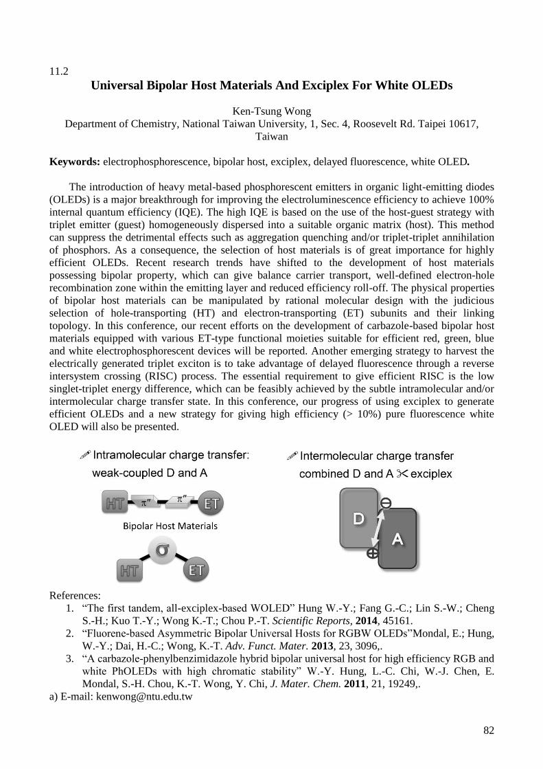
82
11.2
Universal Bipolar Host Materials And Exciplex For White OLEDs
Ken-Tsung Wong
Department of Chemistry, National Taiwan University, 1, Sec. 4, Roosevelt Rd. Taipei 10617,
Taiwan
Keywords: electrophosphorescence, bipolar host, exciplex, delayed fluorescence, white OLED.
The introduction of heavy metal-based phosphorescent emitters in organic light-emitting diodes
(OLEDs) is a major breakthrough for improving the electroluminescence efficiency to achieve 100%
internal quantum efficiency (IQE). The high IQE is based on the use of the host-guest strategy with
triplet emitter (guest) homogeneously dispersed into a suitable organic matrix (host). This method
can suppress the detrimental effects such as aggregation quenching and/or triplet-triplet annihilation
of phosphors. As a consequence, the selection of host materials is of great importance for highly
efficient OLEDs. Recent research trends have shifted to the development of host materials
possessing bipolar property, which can give balance carrier transport, well-defined electron-hole
recombination zone within the emitting layer and reduced efficiency roll-off. The physical properties
of bipolar host materials can be manipulated by rational molecular design with the judicious
selection of hole-transporting (HT) and electron-transporting (ET) subunits and their linking
topology. In this conference, our recent efforts on the development of carbazole-based bipolar host
materials equipped with various ET-type functional moieties suitable for efficient red, green, blue
and white electrophosphorescent devices will be reported. Another emerging strategy to harvest the
electrically generated triplet exciton is to take advantage of delayed fluorescence through a reverse
intersystem crossing (RISC) process. The essential requirement to give efficient RISC is the low
singlet-triplet energy difference, which can be feasibly achieved by the subtle intramolecular and/or
intermolecular charge transfer state. In this conference, our progress of using exciplex to generate
efficient OLEDs and a new strategy for giving high efficiency (> 10%) pure fluorescence white
OLED will also be presented.
References:
1. “The first tandem, all-exciplex-based WOLED” Hung W.-Y.; Fang G.-C.; Lin S.-W.; Cheng
S.-H.; Kuo T.-Y.; Wong K.-T.; Chou P.-T. Scientific Reports, 2014, 45161.
2. “Fluorene-based Asymmetric Bipolar Universal Hosts for RGBW OLEDs”Mondal, E.; Hung,
W.-Y.; Dai, H.-C.; Wong, K.-T. Adv. Funct. Mater. 2013, 23, 3096,.
3. “A carbazole-phenylbenzimidazole hybrid bipolar universal host for high efficiency RGB and
white PhOLEDs with high chromatic stability” W.-Y. Hung, L.-C. Chi, W.-J. Chen, E.
Mondal, S.-H. Chou, K.-T. Wong, Y. Chi, J. Mater. Chem. 2011, 21, 19249,.
a) E-mail: [email protected]
83
11.3
New Schemes for Enhancing the Optical Management and Carrier Transport
Properties of Organic Optoelectronic Devices
Wallace C.H. Choy
Department of Electrical and Electronic Engineering, the University of Hong Kong
Pokfulam Road, Hong Kong
Keywords: plasmonic nanostructure, metal oxide, plasmonic-optical effects, plasmonic-electrical
effects, enhanced electrical properties
A theoretical and experimental study of plasmonic organic solar cells (OSCs) and organic light
emitting diodes (OLEDs) with the metallic nanostructures is presented in this talk. We will firstly discuss
the optical effects of the plasmonic structures and materials effects of the metal nanomaterials (i.e.
plasmonic-optical effects) on enhancing the light absorption of OSCs and emission of OLEDs. We also
study the physics of the performance enhancement is explained by multiphysics model of plasmonic
organic devices. Meanwhile, we propose and demonstrate the enhancement of carrier conduction of
carrier transport layer by two effects. They are the effects of the plasmonically induced carrier generation
and enhanced carrier extraction of the carrier transport layer (i.e. plasmonic-electrical effects) and the
effects of carrier accumulation for filling the trap states of carrier transport layers and thus improving
electrical conduction. With the understanding, we will propose a new plasmonic-electrical concept to
manipulate electrical properties of organic devices including photocarriers recombination, transport and
collection. As a proof-of-concept, OSCs comprising metallic planar and grating electrodes are
systematically investigated with normal and inverted device structures. Interestingly, although strong
plasmonic resonances induce abnormally dense photocarriers around a grating anode, the grating-inverted
OSC is exempt from space charge accumulation (limit) and degradation of electrical properties in
contrast to the planar-inverted and planar-normal ones. The particular reason is that plasmonically
induced photocarriers redistribution shortens the transport path of low-mobility holes, which are collected
by the grating anode. The work demonstrated and explained the space charge limit (SCL) breaking with
the plasmonic-electrical effect. Our results show that the power conversion efficiency of organic solar
cells can be enhanced by over 30% and the value of power conversion efficiency can reach about 9.2%
depending on the metallic nanostructures, device structures, and the polymer materials. Details of the
improvement will be discussed. Consequently, the plasmonic-optical and plasmonic-electrical
effects/concepts will open up a new way to manipulate both optical and electrical properties of
semiconductor devices simultaneously.
We will also introduce novel low-temperature solution-based approaches to fabricate novel carrier
transport layers for the emerging technologies of low-cost and large area photovoltaics. For hole transport
layer, we will demonstrate the common one-step solution approaches applied for MoOx, V2Ox and WOx.
With the approach of intercalation, we can tune the workfunction of the metal oxides by over 1.1eV for
functioning as both electron and hole transport layers in organic optoelectronic devices. For electron
transport layer, we will demonstrate a self-assembly approach to form high quality TiO2. Our results
show that besides OSCs, the carrier transport layer can be applied to other devices such as OLEDs and
dye sensitized solar cells (DSSCs) to improve their performances.
For flexible transparent electrode, we propose and demonstrate a new approach through a low-cost,
robust, room-temperature and atmosphere process to fabricate conductive silver nano-network comprised
of silver nanowires and silver nanoparticles. To be more specific, silver nanoparticles are selectively
grown and chemically integrated in situ at the junction where silver nanowires meet. The site-selective
growth of silver nanoparticles is achieved by plasmon-induced chemical reaction using a simple light
source at very low optical power density. Interestingly, our silver nano-network is readily peeled off in
water which can be easily transferred to other substrates and devices for versatile applications. We
demonstrate the feasibly transferrable silver conductive nano-network as the top electrode in OSCs.
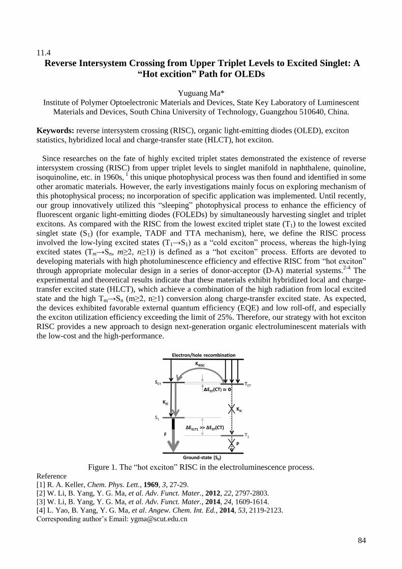
84
11.4
Reverse Intersystem Crossing from Upper Triplet Levels to Excited Singlet: A
“Hot excition” Path for OLEDs
Yuguang Ma*
Institute of Polymer Optoelectronic Materials and Devices, State Key Laboratory of Luminescent
Materials and Devices, South China University of Technology, Guangzhou 510640, China.
Keywords: reverse intersystem crossing (RISC), organic light-emitting diodes (OLED), exciton
statistics, hybridized local and charge-transfer state (HLCT), hot exciton.
Since researches on the fate of highly excited triplet states demonstrated the existence of reverse
intersystem crossing (RISC) from upper triplet levels to singlet manifold in naphthalene, quinoline,
isoquinoline, etc. in 1960s, 1
this unique photophysical process was then found and identified in some
other aromatic materials. However, the early investigations mainly focus on exploring mechanism of
this photophysical process; no incorporation of specific application was implemented. Until recently,
our group innovatively utilized this “sleeping” photophysical process to enhance the efficiency of
fluorescent organic light-emitting diodes (FOLEDs) by simultaneously harvesting singlet and triplet
excitons. As compared with the RISC from the lowest excited triplet state (T1) to the lowest excited
singlet state (S1) (for example, TADF and TTA mechanism), here, we define the RISC process
involved the low-lying excited states (T1→S1) as a “cold exciton” process, whereas the high-lying
excited states (Tm→Sn, m≥2, n≥1)) is defined as a “hot exciton” process. Efforts are devoted to
developing materials with high photoluminescence efficiency and effective RISC from “hot exciton”
through appropriate molecular design in a series of donor-acceptor (D-A) material systems.2-4
The
experimental and theoretical results indicate that these materials exhibit hybridized local and charge-
transfer excited state (HLCT), which achieve a combination of the high radiation from local excited
state and the high Tm→Sn (m≥2, n≥1) conversion along charge-transfer excited state. As expected,
the devices exhibited favorable external quantum efficiency (EQE) and low roll-off, and especially
the exciton utilization efficiency exceeding the limit of 25%. Therefore, our strategy with hot exciton
RISC provides a new approach to design next-generation organic electroluminescent materials with
the low-cost and the high-performance.
Figure 1. The “hot exciton” RISC in the electroluminescence process.
Reference
[1] R. A. Keller, Chem. Phys. Lett., 1969, 3, 27-29.
[2] W. Li, B. Yang, Y. G. Ma, et al. Adv. Funct. Mater., 2012, 22, 2797-2803.
[3] W. Li, B. Yang, Y. G. Ma, et al. Adv. Funct. Mater., 2014, 24, 1609-1614.
[4] L. Yao, B. Yang, Y. G. Ma, et al. Angew. Chem. Int. Ed., 2014, 53, 2119-2123.
Corresponding author’s Email: [email protected]
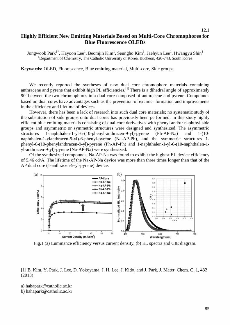
85
12.1
Highly Efficient New Emitting Materials Based on Multi-Core Chromophores for
Blue Fluorescence OLEDs
Jongwook Park1*
, Hayoon Lee1, Beomjin Kim
1, Seungho Kim
1, Jaehyun Lee
1, Hwangyu Shin
1
1Department of Chemistry, The Catholic University of Korea, Bucheon, 420-743, South Korea
Keywords: OLED, Fluorescence, Blue emitting material, Multi-core, Side groups
We recently reported the syntheses of new dual core chromophore materials containing
anthracene and pyrene that exhibit high PL efficiencies.[1]
There is a dihedral angle of approximately
90° between the two chromophores in a dual core composed of anthracene and pyrene. Compounds
based on dual cores have advantages such as the prevention of excimer formation and improvements
in the efficiency and lifetime of devices.
However, there has been a lack of research into such dual core materials; no systematic study of
the substitution of side groups onto dual cores has previously been performed. In this study highly
efficient blue emitting materials consisting of dual core derivatives with phenyl and/or naphthyl side
groups and asymmetric or symmetric structures were designed and synthesized. The asymmetric
structures 1-naphthalen-1-yl-6-(10-phenyl-anthracen-9-yl)-pyrene (Ph-AP-Na) and 1-(10-
naphthalen-1-ylanthracen-9-yl)-6-phenyl-pyrene (Na-AP-Ph), and the symmetric structures 1-
phenyl-6-(10-phenylanthracen-9-yl)-pyrene (Ph-AP-Ph) and 1-naphthalen-1-yl-6-(10-naphthalen-1-
yl-anthracen-9-yl)-pyrene (Na-AP-Na) were synthesized.
Of the synthesized compounds, Na-AP-Na was found to exhibit the highest EL device efficiency
of 5.46 cd/A. The lifetime of the Na-AP-Na device was more than three times longer than that of the
AP dual core (1-anthracen-9-yl-pyrene) device.
Fig.1 (a) Luminance efficiency versus current density, (b) EL spectra and CIE diagram.
[1] B. Kim, Y. Park, J. Lee, D. Yokoyama, J. H. Lee, J. Kido, and J. Park, J. Mater. Chem. C, 1, 432
(2013)

86
12.2
Aggregation-Induced Emission
Ben Zhong Tang*
Department of Chemistry and Division of Biomedical Engineering, The Hong Kong University of
Science and Technology, Clear Water Bay, Kowloon, Hong Kong , China
Typical chromophores usually suffer from weakening or quenching of light emission caused by
aggregation. This notorious photophysical effect is practically harmful, as luminophores are
commonly used for real-world applications in solid state or aqueous media, where chromophores
tend to form aggregates. We have discovered a diametrically opposite phenomenon that
chromophores are non-emissive when molecularly dissolved and induced to luminesce by aggregate
formation. We termed this unusual process as aggregation-induced emission (AIE) and identified the
restriction of intramolecular motion (RIM) as the main cause for the AIE effect. Based on the RIM
mechanism, we have developed a wide variety of AIE luminogens with broad emission range
covering visible and near-IR region and high luminescence quantum yields. We have demonstrated
the great utility of the AIE systems and explored their high-tech applications in such areas as
optoelectronic devices, chemo/biosensing and biological imaging.
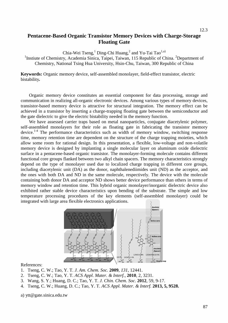
87
12.3
Pentacene-Based Organic Transistor Memory Devices with Charge-Storage
Floating Gate
Chia-Wei Tseng,1 Ding-Chi Huang,
2 and Yu-Tai Tao
1,a)
1Instiute of Chemistry, Academia Sinica, Taipei, Taiwan, 115 Republic of China.
2Department of
Chemistry, National Tsing Hua University, Hsin-Chu, Taiwan, 300 Republic of China
Keywords: Organic memory device, self-assembled monolayer, field-effect transistor, electric
bistability.
Organic memory device constitutes an essential component for data processing, storage and
communication in realizing all-organic electronic devices. Among various types of memory devices,
transistor-based memory device is attractive for structural integration. The memory effect can be
achieved in a transistor by inserting a charge-trapping floating gate between the semiconductor and
the gate dielectric to give the electric bistability needed in the memory function.
We have assessed carrier traps based on metal nanoparticles, conjugate diacetylenic polymer,
self-assembled monolayers for their role as floating gate in fabricating the transistor memory
device.1-4
The performance characteristics such as width of memory window, switching response
time, memory retention time are dependent on the structure of the charge trapping moieties, which
allow some room for rational design. In this presentation, a flexible, low-voltage and non-volatile
memory device is designed by implanting a single molecular layer on aluminum oxide dielectric
surface in a pentacene-based organic transistor. The monolayer-forming molecule contains different
functional core groups flanked between two alkyl chain spacers. The memory characteristics strongly
depend on the type of monolayer used due to localized charge trapping in different core groups,
including diacetylenic unit (DA) as the donor, naphthalenediimides unit (ND) as the acceptor, and
the ones with both DA and ND in the same molecule, respectively. The device with the molecule
containing both donor DA and acceptor ND shows better device performance than others in terms of
memory window and retention time. This hybrid organic monolayer/inorganic dielectric device also
exhibited rather stable device characteristics upon bending of the substrate. The simple and low
temperature processing procedures of the key elements (self-assembled monolayer) could be
integrated with large area flexible electronics applications.
References:
1. Tseng, C. W.; Tao, Y. T. J. Am. Chem. Soc. 2009, 131, 12441.
2. Tseng, C. W.; Tao, Y. T. ACS Appl. Mater. & Interf., 2010, 2, 3231.
3. Wang, S. Y.; Huang, D. C.; Tao, Y. T. J. Chin. Chem. Soc. 2012, 59, 9-17.
4. Tseng, C. W.; Huang, D. C.; Tao, Y. T. ACS Appl. Mater. & Interf. 2013, 5, 9528.

88
Abstract of Posters

89
P-01
A-D-A Type Organic Dyes Employing Coplanar Heteroarene for Efficient Small
Molecule Organic Solar Cells
Chin-Lung Chung1,a)
, Chien-Yu Chen2, Hao-Wei Kang
2, Hao-Wu Lin
2,b), Ken-Tsung Wong
1,b)
1 Department of Chemistry, National Taiwan University, Taipei, Taiwan
2 Department of Materials Science and Engineering, National Tsing Hua University, Hsin Chu,
Taiwan
Keywords: fused system, coplanar, rigid, heteroacene, organic solar cells
Organic solar cells (OSCs) have attracted great attention in recent years because of their
potential advantages such as cost effective fabrication, mechanical flexibility, color-tunable feature,
and low environmental impact production which make them as possible alternative to the
conventional Si-based solar cells.1 The molecular design strategies of efficient electron donors in
OSCs generally involve the combination of electron-rich group and electron-deficient group to
facilitate effective intramolecular charge transfer (ICT) which can reduce the bandgaps of molecules
and extend the absorption spectrum towards longer wavelength. Among various molecular
architectures, photovoltaic devices utilized the molecules adopting symmetrical acceptor-donor-
acceptor (A-D-A) configuration have achieved promising performance. On the other hand, ladder-
type -conjugated molecules with fully-fused coplanar backbone are emerging as a new class of
compounds for organic optoelectronics because of their diverse and interesting properties such as
intense photoluminescence and high carrier mobility.2 Accordingly, we used the fused pentacyclic
and hexacyclic heteroacenes as donor moieties and dicyanovinylene as acceptor to synthesize new
organic dyes DTPTDCV and DTPTtDCV (Fig. 1). The incorporation of rigid and coplanar features
into the donor-acceptor system can enhance -electron delocalization and elongate effective
conjugation length, resulting in higher photocurrent due to a better spectral response. Moreover, the
stiff molecular frameworks can suppress the conformational disorder and reduce the reorganization
energy upon electron transfer, destined to enhance intrinsic charge mobility. As a result, the solar
cells based on DTPTtDCV shows a power conversion efficiency (PCE) of 3.02% and the device
based on DTPTDCV performing a PCE up to 5.64% was achieved. The results will be presented in
this conference.
Fig. 1
(1) S. B. Darling; F. You, RSC Advances, 2013, 3, 17633.
(2) A. Fukazawa; S. Yamaguchi, Chem. Asian J., 2009, 4, 1386.
a) [email protected] b) [email protected]; [email protected]

90
P-02
Highly flexible bending deformation in single crystalline diamond nanoneedles
for biomedical applications
Amit Banerjee1,3,a),*
, Zhang Hongti1,*
, Yuen Muk Fung2,3
, Zhang Wenjun2, 3
, Lu Yang1,3,b)
1 Department of Mechanical and Biomedical Engineering, City University of Hong Kong, Hong
Kong 2 Department of Physics and Materials Science, City University of Hong Kong, Hong Kong
3 Center for Super-Diamond and Advanced Films, City University of Hong Kong, Hong Kong
Keywords: Diamond structure, Nanoneedle, brittle failure, flexural deformation, Nanomechanics.
Through in situ investigations performed by a quantitative nanoindenter inside a scanning
electron microscope (SEM), we report that single crystalline cone-shaped artificial diamond
nanomaterial (nanoneedles), fabricated by plasma assisted deposition and etching, can undergo
highly flexible and reversible bending deformation before experiencing brittle failure. The
dimensions of the nanoneedles utilized during the present experiments belong to the following
ranges, length: 0.5 – 3 µm, base diameter: 200 – 900 nm, and the tip diameter: 50 – 150 nm
respectively. Through systematic mechanical characterizations conducted by indentation,
compression, and flexural deformation modes, the mechanical properties of diamond nanoneedles
are evaluated. The material is observed to retain its high hardness and Young’s modulus, in addition
the nanoneedles are observed to obtain as much as 13 – 19 % local flexural strain at failure. Due to
the in situ nature of the experiments, the visuals of the bending deformation and the failure
mechanism of the nanoneedles under loading and unloading cycles are revealed and correlated with
classical beam theory. These nanoneedles have recently been shown to find promising applications in
intracellular drug delivery by several groups.
a) Presenting author’s Email: [email protected]
b) Corresponding author’s Email: [email protected]
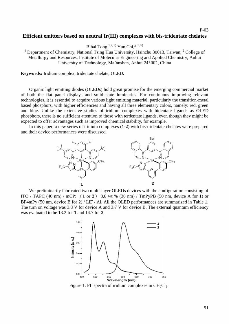
91
P-03
Efficient emitters based on neutral Ir(III) complexes with bis-tridentate chelates
Bihai Tong,1,2, a)
Yun Chi,*,1, b)
1 Department of Chemistry, National Tsing Hua University, Hsinchu 30013, Taiwan,
2 College of
Metallurgy and Resources, Institute of Molecular Engineering and Applied Chemistry, Anhui
University of Technology, Ma’anshan, Anhui 243002, China
Keywords: Iridium complex, tridentate chelate, OLED.
Organic light emitting diodes (OLEDs) hold great promise for the emerging commercial market
of both the flat panel displays and solid state luminaries. For continuous improving relevant
technologies, it is essential to acquire various light emitting material, particularly the transition-metal
based phosphors, with higher efficiencies and having all three elementary colors, namely: red, green
and blue. Unlike the extensive studies of iridium complexes with bidentate ligands as OLED
phosphors, there is no sufficient attention to those with terdentate ligands, even though they might be
expected to offer advantages such as improved chemical stability, for example.
In this paper, a new series of iridium complexes (1-2) with bis-tridentate chelates were prepared
and their device performances were discussed.
NIr
N
F F
N
N
1
NF3C
CF3
NIr
N
N
N
2
NF3C
CF3
But
We preliminarily fabricated two multi-layer OLEDs devices with the configuration consisting of
ITO / TAPC (40 nm) / mCP: (1 or 2) 8.0 wt % (30 nm) / TmPyPB (50 nm, device A for 1) or
BP4mPy (50 nm, device B for 2) / LiF / Al. All the OLED performances are summarized in Table 1.
The turn on voltage was 3.8 V for device A and 3.7 V for device B. The external quantum efficiency
was evaluated to be 13.2 for 1 and 14.7 for 2.
450 500 550 600 650 700 750
0.0
0.2
0.4
0.6
0.8
1.0
Inte
nsi
ty (
a. u
.)
Wavelength (nm)
1
2
Figure 1. PL spectra of iridium complexes in CH2Cl2.

92
Table 1. Performances of the electrophosphorescnt devices. Device ηxt[
%]
ηl[cd/
A]
ηp[lm
/W]
Von (@ 1
cd/m2)
CIE [x, y]
(@ 100 cd/m2)
Lmax
[cd/m2]
A Peak 13.2 41.4 35.5 3.8 V (0.305, 0.582) 15787
(11.0 V) 100
cd/m2
13.0 40.7 26.6
B Peak 14.7 21.8 21.9 3.7 V (0.628, 0.368) 24416
(13.4 V) 100
cd/m2
13.6 20.1 11.2
In summary, we have developed a new series iridium complexes and demonstrated that good
OLED performance is possible using such complexes.
References
[1] C. H. Lin, Y. Y. Chang, J.Y. Hung, et al., Angew. Chem. Int. Ed. 2011, 50, 3182 -3186.
[2] C. H. Lin, Y. Y. Chang, J. Y. Hung, et al., Inorg. Chem. 2012, 51, 1785-1795.

93
P-04
Deep Blue Emission p-n Type Polyfluorenes with Steric Hindrance Effects,
Exhibiting Excellent Thermal, Morphology and Spectra Stability LIU Bin
1,a), ZHU Wensai
2, LIN Jinyi
2, XIE Linghai*
1, HUANG Wei*
1,2,b)
1 Key Laboratory for Organic Electronics & Information Displays (KLOEID) and Institute of
Advanced Materials (IAM), Nanjing University of Posts &Telecommunications, Nanjing 210023, P.
R. China., 2 Jiangsu-Singapore Joint Research Center for Organic/Bio Electronics & Information Displays,
Institute of Advanced Materials (IAM), Nanjing Tech University, Nanjing 211816, P. R. China.
Keywords: Fluorinated, steric hindrance effects, p-n type, polyfluorenes, stability.
P-n copolymerization serves as the most effective toolbox to tune the properties both inter and intra
molecules in plastic semiconductor materials. Here, a serial of polyfluorenes containing
tetrafluorobenzene were synthesized by facile palladium-based direct aromatization. The band gap of
the poly (2,7-fluorene-co-alt-1,4-tetrafluorobenzene)s poly(PFs-alt-TFP) were broadened expectedly
by incorporating electronic deficient tetrafluorobenzene, exhibiting a deep blue emission and low
HOMO energy level, which enhanced the antioxidant capacity. The polymers with steric hindrance
effects all showed excellent stability, including thermal, spectra and morphology, compared to 9,9-
dioctylfluoene one. Therefore, p-n type polyfluorenes with steric hindrance effects prepared by direct
aromatization is promising strategy for stable solution processing semiconductors for commercial
applications.
Figure 1. The UV and PL spectra was obtained from spin-coated film (f) and dilute solution (s),
respectively; the annealing PL spectra was obtained from film after 180oC in air for 8 hours; the
AFM images stand for pristine film (upper) and film under annealing for 180oC in air for 3 hours
(down).

94
P-05
Enhanced Self-Assembled Monolayer Treatment on Polymer Insulator for
Organic Field-effect Transistor
Yan Yan a), and V. A. L Roy
b)
Department of Physics and Materials Science, City University of Hong Kong, Hong Kong SAR;
Poly-4-vinylphenol, poly(methyl methacrylate) and cross-linked PVP are employed as polymeric
insulator and chemical vapor deposition is used to form self-assembled monolayer on polymeric
insulators surface. An ordered molecular orientation is formed with larger grains resulting in
improved carrier mobilities, and low threshold voltages (VT) with self-assembled monolayer on
polymeric dielectrics. Moreover, ultraviolet/ozone (UVO) treatment is ultized to enhance the
alignment of HMDS monolayer on polymeric insulator surface and a time dependent effect is
observed for UV/ozone treatment. For PVP and cross-linked PVP substrates, a short UVO exposure
enhances the HMDS reaction on the polymer surface, and a long UVO exposure shows an adverse
effect. On the other hand, PMMA is found to be more sensitive to UVO treatment and displayed
performance degradation. These findings will be of value for solution processed insulators for
printable electronic applications on flexible substrates.
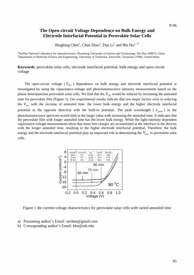
95
P-06
The Open-circuit Voltage Dependence on Bulk Energy and
Electrode Interfacial Potential in Perovskite Solar Cells
Bingbing Chen1, Chen Zhao
1, Dan Li
1 and Bin Hu
1, 2*
1WuHan National Laboratory for Optoelectronics, Huazhong University of Science and Technology, Wu Han 430074, China 2Department of Materials Science and Engineering, University of Tennessee, Knoxville, Tennessee 37996, United States
Keywords: perovskite solar cells, electrode interfacial potential, bulk energy and open-circuit
voltage
The open-circuit voltage ( OCV ) dependence on bulk energy and electrode interfacial potential is
investigated by using the capacitance-voltage and photoluminescence intensity measurements based on the
planar heterojunction perovskite solar cells. We find that the OCV would be reduced by increasing the annealed
time for perovskite film (Figure 1). Our experimental results indicate that two major factors exist in reducing
the OCV with the increase of annealed time: the lower bulk energy and the higher electrode interfacial
potential in the opposite direction with the built-in potential. The peak wavelength ( peak ) in the
photoluminescence spectrum would shift to the larger value with increasing the annealed time. It indicates that
the perovskite film with longer annealed time has the lower bulk energy. While the light-intensity dependent
capacitance-voltage measurements show that more free charges are accumulated at the interface in the devices
with the longer annealed time, resulting in the higher electrode interfacial potential. Therefore, the bulk
energy and the electrode interfacial potential play an important role in determining the OCV in perovskite solar
cells.
Figure 1 the current-voltage characteristics for perovskite solar cells with varied annealed time
a) Presenting author’s Email: [email protected]
b) Corresponding author’s Email: [email protected]
-0.2 0.0 0.2 0.4 0.6 0.8 1.0
-20
-16
-12
-8
-4
0
4
8
90 min
75 min
Cu
rre
nt
(mA
/cm
2)
Voltage (V)
60 min
80 0C
anneal ti Voc (mV) Jsc FF(%) PCE(%)
60min 952 14.26 65.2 8.85
75 min 927 16.38 64.3 9.76
90 min 892 19.15 58.2 9.94
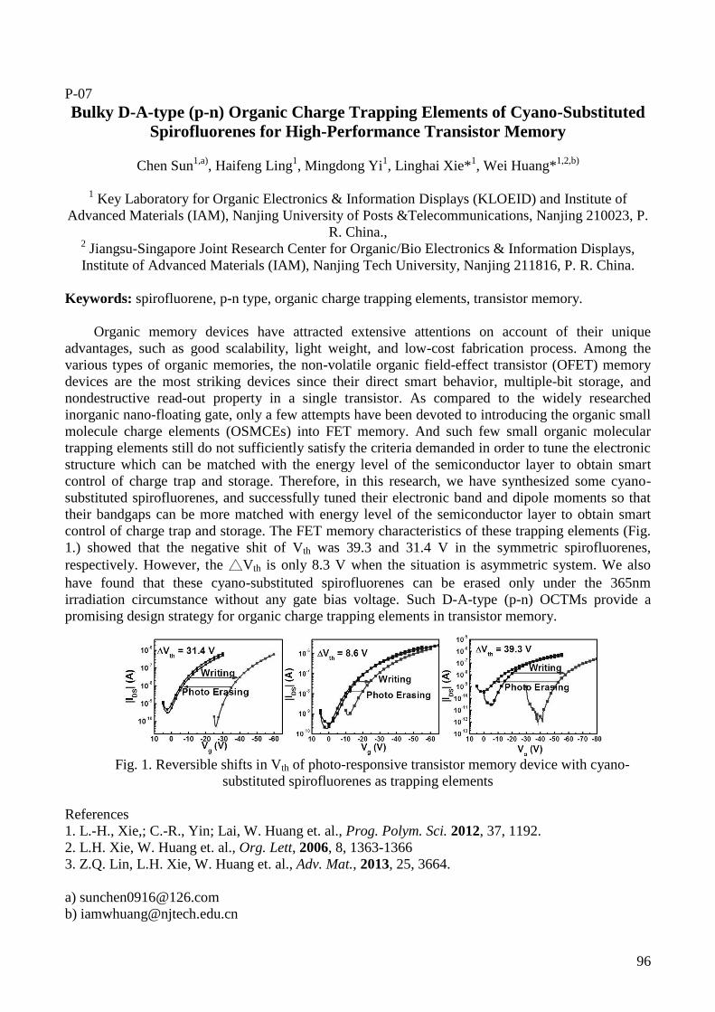
96
P-07
Bulky D-A-type (p-n) Organic Charge Trapping Elements of Cyano-Substituted
Spirofluorenes for High-Performance Transistor Memory
Chen Sun1,a)
, Haifeng Ling1, Mingdong Yi
1, Linghai Xie*
1, Wei Huang*
1,2,b)
1 Key Laboratory for Organic Electronics & Information Displays (KLOEID) and Institute of
Advanced Materials (IAM), Nanjing University of Posts &Telecommunications, Nanjing 210023, P.
R. China., 2 Jiangsu-Singapore Joint Research Center for Organic/Bio Electronics & Information Displays,
Institute of Advanced Materials (IAM), Nanjing Tech University, Nanjing 211816, P. R. China.
Keywords: spirofluorene, p-n type, organic charge trapping elements, transistor memory.
Organic memory devices have attracted extensive attentions on account of their unique
advantages, such as good scalability, light weight, and low-cost fabrication process. Among the
various types of organic memories, the non-volatile organic field-effect transistor (OFET) memory
devices are the most striking devices since their direct smart behavior, multiple-bit storage, and
nondestructive read-out property in a single transistor. As compared to the widely researched
inorganic nano-floating gate, only a few attempts have been devoted to introducing the organic small
molecule charge elements (OSMCEs) into FET memory. And such few small organic molecular
trapping elements still do not sufficiently satisfy the criteria demanded in order to tune the electronic
structure which can be matched with the energy level of the semiconductor layer to obtain smart
control of charge trap and storage. Therefore, in this research, we have synthesized some cyano-
substituted spirofluorenes, and successfully tuned their electronic band and dipole moments so that
their bandgaps can be more matched with energy level of the semiconductor layer to obtain smart
control of charge trap and storage. The FET memory characteristics of these trapping elements (Fig.
1.) showed that the negative shit of Vth was 39.3 and 31.4 V in the symmetric spirofluorenes,
respectively. However, the △Vth is only 8.3 V when the situation is asymmetric system. We also
have found that these cyano-substituted spirofluorenes can be erased only under the 365nm
irradiation circumstance without any gate bias voltage. Such D-A-type (p-n) OCTMs provide a
promising design strategy for organic charge trapping elements in transistor memory.
Fig. 1. Reversible shifts in Vth of photo-responsive transistor memory device with cyano-
substituted spirofluorenes as trapping elements
References
1. L.-H., Xie,; C.-R., Yin; Lai, W. Huang et. al., Prog. Polym. Sci. 2012, 37, 1192.
2. L.H. Xie, W. Huang et. al., Org. Lett, 2006, 8, 1363-1366
3. Z.Q. Lin, L.H. Xie, W. Huang et. al., Adv. Mat., 2013, 25, 3664.
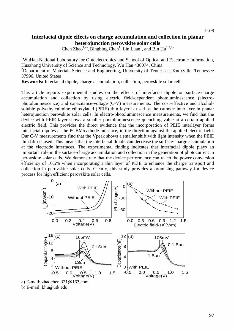
97
P-08
Interfacial dipole effects on charge accumulation and collection in planar
heterojunction perovskite solar cells Chen Zhao
1,a), Bingbing Chen
1, Lin Luan
1, and Bin Hu
1,2,b)
1WuHan National Laboratory for Optoelectronics and School of Optical and Electronic Information,
Huazhong University of Science and Technology, Wu Han 430074, China 2Department of Materials Science and Engineering, University of Tennessee, Knoxville, Tennessee
37996, United States
Keywords: Interfacial dipole, charge accumulation, collection, perovskite solar cells
This article reports experimental studies on the effects of interfacial dipole on surface-charge
accumulation and collection by using electric field-dependent photoluminescence (electro-
photoluminescence) and capacitance-voltage (C-V) measurements. The cost-effective and alcohol-
soluble polyethylenimine ethoxylated (PEIE) thin layer is used as the cathode interlayer in planar
heterojunction perovskite solar cells. In electro-photoluminescence measurements, we find that the
device with PEIE layer shows a smaller photoluminescence quenching value at a certain applied
electric field. This provides the direct evidence that the incorporation of PEIE interlayer forms
interfacial dipoles at the PCBM/cathode interface, in the direction against the applied electric field.
Our C-V measurements find that the Vpeak shows a smaller shift with light intensity when the PEIE
thin film is used. This means that the interfacial dipole can decrease the surface-charge accumulation
at the electrode interfaces. The experimental finding indicates that interfacial dipole plays an
important role in the surface-charge accumulation and collection in the generation of photocurrent in
perovskite solar cells. We demonstrate that the device performance can reach the power conversion
efficiency of 10.5% when incorporating a thin layer of PEIE to enhance the charge transport and
collection in perovskite solar cells. Clearly, this study provides a promising pathway for device
process for high efficient perovskite solar cells.
a) E-mail: [email protected]
b) E-mail: [email protected]
-0.5 0.0 0.5 1.0 1.5
0
4
8
12
16
1Sun
Ca
pa
cita
nce
(nF
)
Voltage(V)
0.1Sun
165mV(c)
Without PEIE
-0.5 0.0 0.5 1.0 1.5
0
4
8
12
With PEIE
1 Sun
Ca
pa
cita
nce
(nF
)
Voltage(V)
0.1 Sun
105mV(d)
0.0 0.3 0.6 0.9 1.2 1.5
-60
-30
0
With PEIE
PL
cha
ng
e(%
)
Electric field(V/m)
Without PEIE
(b)
0.0 0.2 0.4 0.6 0.8
-20
-10
0
With PEIE
I SC(m
A/c
m2)
Voltage(V)
Without PEIE
(a)

98
P-09
High-cycle fatigue testing of individual nanowires based on DMD
JIANG Chenchen1,3,a)
, LU Yang1, 2,3, b)
1Department of Mechanical and Biomedical Engineering, City University of Hong Kong
2Center of Super-Diamond and Advanced Films, City University of Hong Kong
3Center for Advanced Structural Materials, City University of Hong Kong
Keywords: fatigue, in situ mechanical testing, MEMS, nanowire, DMD.
Nanowires have been used in more and more applications, such as next generation bio-sensors and
flexible electronics. However, the reliability and the lifetime of such devices undergoing repeated
cyclic loading highly depend on the nanowires’ fatigue performance. Despite extensive research into
the mechanical properties of one-dimensional nanomaterials, such as metallic/semiconductor
nanowires and carbon nanotubes, for the past two decades, experimental data on the fatigue behavior
of these 1-D nanostructures have rarely been reported, especially for high cyclic fatigue. Recently,
MEMS-based devices had been developed and adopted for testing low-dimensional nanostructures.
Here, instead of designing a dedicated MEMS device, we propose to adopt a commercially available
MEMS product ---DMD (Digital Micromirror Device, by Texas Instruments) for the development of
a novel nano-fatigue testing platform. The ultimate goal of this research is establish an entirely new
platform for high-cycle fatigue study of individual 1-D nanomaterials, and to offer some critical
insights into the fatigue mechanisms and life prediction for nanowire/nanotube-based electronic
device applications.
a) Presenting author: [email protected]
b) Corresponding author: [email protected]

99
P-10
Bipolar spin-filtering, rectifying and giant magnetoresistance effects in zigzag
silicene nanoribbons with asymmetric edge hydrogenation
Dan Zhang1,a)
, Meng-Qiu Long1,2,b)
, Hui Xu1, Kowksum Chan
2
1Institute of Super-microstructure and Ultrafast Process in Advanced Materials, School of Physics
and Electronics, Central South University, Changsha 410083, China 2Department of Physics and Materials Science, City University of Hong Kong, Hong Kong, China
Keywords: zigzag silicene nanoribbons, asymmetric edge hydrogenation, bipolar spin-filtering,
rectifying behavior, giant magnetoresistance
Graphene, one monolayer of sp2-bonded carbon tightly packed into a two-dimensional honeycomb
lattice, has drawn numerous attention as a hopeful candidate material for spintronic devices due to its
high electronic mobility, gate tunability, magnetic zigzag edges and unique transport properties [1,2].
But there still exist many technical barriers in combining carbon based graphene with silicon based
modern electronic industry. At this time, silicene--a material isostructural to graphene but with
atomic bonds that are buckled rather than flat has been synthesized and attracts enormous research
attention [3,4]. Former researches show that the silicene features a Dirac-like electron dispersion at
the K points of the Brillouin zone and exhibits exciting properties beyond those present in graphene
[5,6].
Usually, silicene are tailored into nanoribbons in practical applications. And it can mainly be
classified into zigzag silicene nanoribbons (ZSiNRs) and armchair silicene nanoribbons (ASiNRs).
ASiNRs are semiconductors, and the band gap oscillates with a period 3 dimers when ribbon width
increases [7]. While the ZSiNRs have stable antiferromagnetic(AFM) states, and it can become half-
metals under an external transverse electric fields [8]. When comes to the transport properties of
ZSiNRs, they also posses the same symmetry-dependent properties although they have a buckled
structure, and the giant magnetoresistance has been predicted in ZSiNRs connected to two semi-
infinite silicene electrodes [9]. The amazing properties of ZSiNRs could give rise to many promising
applications in silicon based spintronic technology. However, ZSiNRs display spin degeneracy in the
AFM state, which limits their application in spintronic devices. Presently, there are many methods
which can be used to break the spin degeneracy, such as an electric field, doping, defects, and edge
modifying [10-12]. In particular, the asymmetric edge hydrogenation, which corresponds to the two
edges with different hybridizations (i.e. sp2 and sp
3 edges), could bring diverse magnetic properties
in the silicene nanoribbons, and has attracted the research interest of many researchers recently [13].
Theoretical studies have demonstrated that ZSiNRs with asymmetric edge hydrogenation are more
stable than symmetric single H saturation. Moreover, ZSiNRs with asymmetric edge hydrogenation
are bipolar magnetic semiconductors and can be changed to half-metals by doping and strain [14].
The edge states can significantly affect the nanoribbons' electronic and magnetic properties, but how
the asymmetric edge hydrogenation affects the transport properties of ZSiNRs remains completely
unclear. Therefore we are mainly focusing on the spin-dependent transport properties of the
asymmetric edge hydrogenated ZSiNRs with parallel (P) and antiparallel (AP) magnetic
configurations.
Using the nonequilibrium Green’s function method and the spin-polarized density functional
theory, the spin-dependent electronic transport properties of ZSiNRs with asymmetric edge
hydrogenation have been studied. The results show that there exists nearly 100% bipolar spin-
filtering behavior in the ZSiNR-based devices with AP spin configuration. Moreover, spin rectifying
behavior as high as 3400 and giant magnetoresistance with the order of 108
% are found in the
devices. Our calculation suggests ZSiNRs with asymmetric edge hydrogenation as a promising
candidate material for spintronics.

100
References [1] Phys. Rev. Lett. 97, 216803(2006).
[2] Phys. Rev. Lett. 100, 206802(2008).
[3] Phys. Rev. Lett. 108, 245501 (2012).
[4] RSC Adv. 3, 13772 (2013).
[5] Phys. Rev. B 87,241409(R) (2013).
[6] J. Phys.: Cond. Matt. 24, 455302(2012).
[7] Phys. Rev. Lett. 102, 236804 (2009).
[8] Appl. Phys. Lett. 95, 083115 (2009).
[9] Appl. Phys. Lett. 100, 233122 (2012).
[10] J. Appl. Phys. 114, 163711 (2013).
[11] J. Phys. Chem. C 117, 13620 (2013).
[12] Appl. Phys. Lett. 104, 083111 (2014). [13] Appl. Phys. Lett. 102, 143115(2013).
[14] RSC Adv. 3, 24075 (2013).
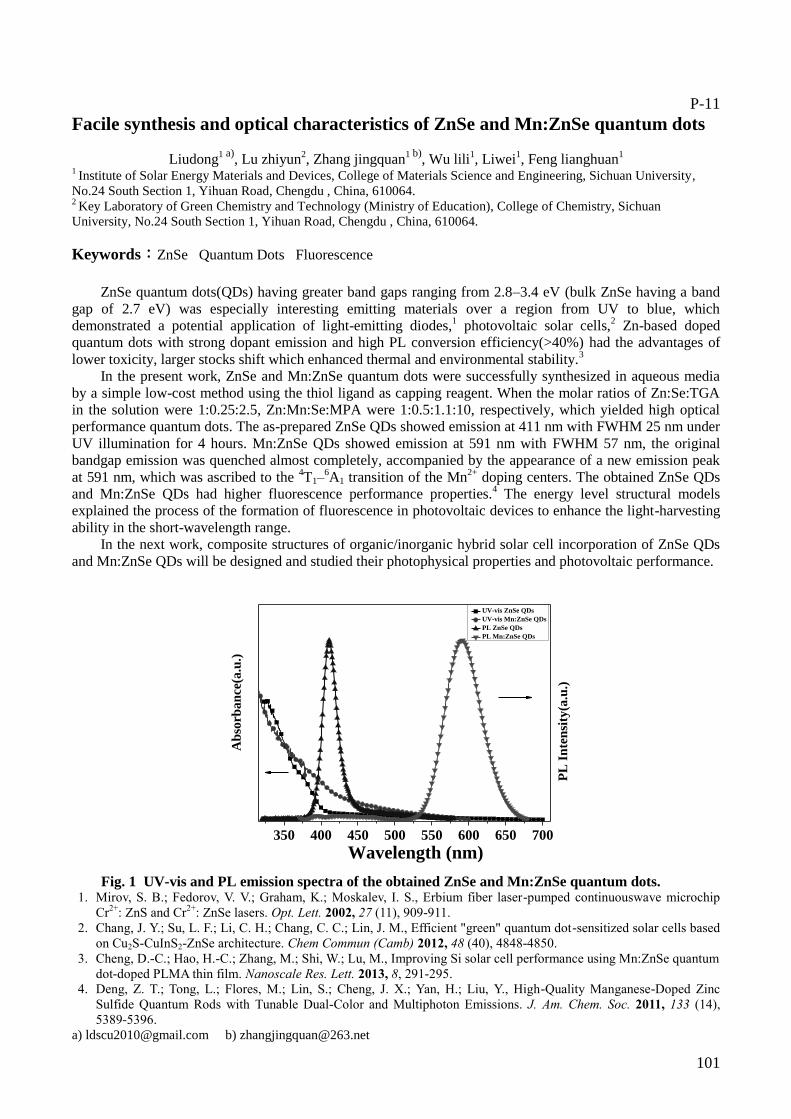
101
P-11
Facile synthesis and optical characteristics of ZnSe and Mn:ZnSe quantum dots
Liudong1 a)
, Lu zhiyun2, Zhang jingquan
1 b), Wu lili
1, Liwei
1, Feng lianghuan
1
1 Institute of Solar Energy Materials and Devices, College of Materials Science and Engineering, Sichuan University,
No.24 South Section 1, Yihuan Road, Chengdu , China, 610064. 2 Key Laboratory of Green Chemistry and Technology (Ministry of Education), College of Chemistry, Sichuan
University, No.24 South Section 1, Yihuan Road, Chengdu , China, 610064.
Keywords:ZnSe Quantum Dots Fluorescence
ZnSe quantum dots(QDs) having greater band gaps ranging from 2.8–3.4 eV (bulk ZnSe having a band
gap of 2.7 eV) was especially interesting emitting materials over a region from UV to blue, which
demonstrated a potential application of light-emitting diodes,1 photovoltaic solar cells,
2 Zn-based doped
quantum dots with strong dopant emission and high PL conversion efficiency(>40%) had the advantages of
lower toxicity, larger stocks shift which enhanced thermal and environmental stability.3
In the present work, ZnSe and Mn:ZnSe quantum dots were successfully synthesized in aqueous media
by a simple low-cost method using the thiol ligand as capping reagent. When the molar ratios of Zn:Se:TGA
in the solution were 1:0.25:2.5, Zn:Mn:Se:MPA were 1:0.5:1.1:10, respectively, which yielded high optical
performance quantum dots. The as-prepared ZnSe QDs showed emission at 411 nm with FWHM 25 nm under
UV illumination for 4 hours. Mn:ZnSe QDs showed emission at 591 nm with FWHM 57 nm, the original
bandgap emission was quenched almost completely, accompanied by the appearance of a new emission peak
at 591 nm, which was ascribed to the 4T1–
6A1 transition of the Mn
2+ doping centers. The obtained ZnSe QDs
and Mn:ZnSe QDs had higher fluorescence performance properties.4 The energy level structural models
explained the process of the formation of fluorescence in photovoltaic devices to enhance the light-harvesting
ability in the short-wavelength range.
In the next work, composite structures of organic/inorganic hybrid solar cell incorporation of ZnSe QDs
and Mn:ZnSe QDs will be designed and studied their photophysical properties and photovoltaic performance.
350 400 450 500 550 600 650 700
PL
In
ten
sity
(a.u
.)
Ab
sorb
an
ce(a
.u.)
Wavelength (nm)
UV-vis ZnSe QDs
UV-vis Mn:ZnSe QDs
PL ZnSe QDs
PL Mn:ZnSe QDs
Fig. 1 UV-vis and PL emission spectra of the obtained ZnSe and Mn:ZnSe quantum dots.
1. Mirov, S. B.; Fedorov, V. V.; Graham, K.; Moskalev, I. S., Erbium fiber laser-pumped continuouswave microchip
Cr2+
: ZnS and Cr2+
: ZnSe lasers. Opt. Lett. 2002, 27 (11), 909-911.
2. Chang, J. Y.; Su, L. F.; Li, C. H.; Chang, C. C.; Lin, J. M., Efficient "green" quantum dot-sensitized solar cells based
on Cu2S-CuInS2-ZnSe architecture. Chem Commun (Camb) 2012, 48 (40), 4848-4850.
3. Cheng, D.-C.; Hao, H.-C.; Zhang, M.; Shi, W.; Lu, M., Improving Si solar cell performance using Mn:ZnSe quantum
dot-doped PLMA thin film. Nanoscale Res. Lett. 2013, 8, 291-295.
4. Deng, Z. T.; Tong, L.; Flores, M.; Lin, S.; Cheng, J. X.; Yan, H.; Liu, Y., High-Quality Manganese-Doped Zinc
Sulfide Quantum Rods with Tunable Dual-Color and Multiphoton Emissions. J. Am. Chem. Soc. 2011, 133 (14),
5389-5396.
102
P-12
Long operation lifetime and colour stable hybrid tandem white organic light-
emitting diodes for general lighting
F. L. Wonga)
, M. K. Fung, C.S. Leeb)
Center of Super-Diamond & Advanced Thin Films (COSDAF) and Department of Physics &
Materials Science, City University of Hong Kong, Tat Chee Avenue, Hong Kong, SAR, PR China
Keywords: electroluminescence, hybrid, organic, stack, tandem
A fluorescence blue emitting unit and a phosphorescence orange-green emitting unit were
stacked to form a hybrid tandem white organic light-emitting diode (WOLED). Charge generating
layers were inserted between the 2 emitting units. Firstly, the colour outputs of the devices were
controlled by varying the concentration of the blue dopant in the device. With optimum blue dopant
concentration, C.I.E. coordinates of (0.48, 0.44), (0.42, 0.40) and (0.38, 0.37) were obtained at 7 V,
10 V and 15 V respectively. To further improve the white coordinates and the colour stability, a layer
of 2,2',2"-(1,3,5-benzinetriyl)-tris(1-phenyl-1-H-benzimidazole) (TPBi) was inserted between the
electron injection layer and the electron transport layer in the blue emitting unit. With optimum
interface engineering, C.I.E. coordinates of (0.39, 0.39), (0.35, 0.36), (0.33, 0.34) were obtained at 7
V, 10 V and 15 V respectively. In this paper, color stable hybrid tandem WOLED with maximum
power efficiency of 60 lm/W and operation lifetime of 200,000 hours were reported.
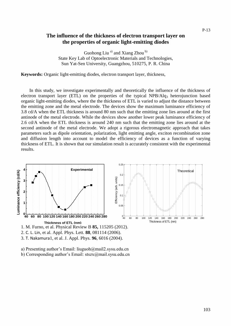
103
P-13
The influence of the thickness of electron transport layer on
the properties of organic light-emitting diodes
Guohong Liu a)
and Xiang Zhou b)
State Key Lab of Optoelectronic Materials and Technologies,
Sun Yat-Sen University, Guangzhou, 510275, P. R. China
Keywords: Organic light-emitting diodes, electron transport layer, thickness,
In this study, we investigate experimentally and theoretically the influence of the thickness of
electron transport layer (ETL) on the properties of the typical NPB/Alq3 heterojunction based
organic light-emitting diodes, where the the thickness of ETL is varied to adjust the distance between
the emitting zone and the metal electrode. The devices show the maximum luminance efficiency of
3.8 cd/A when the ETL thickness is around 80 nm such that the emitting zone lies around at the first
antinode of the metal electrode. While the devices show another lower peak luminance efficiency of
2.6 cd/A when the ETL thickness is around 240 nm such that the emitting zone lies around at the
second antinode of the metal electrode. We adopt a rigorous electromagnetic approach that takes
parameters such as dipole orientation, polarization, light emitting angle, exciton recombination zone
and diffusion length into account to model the efficiency of devices as a function of varying
thickness of ETL. It is shown that our simulation result is accurately consistent with the experimental
results.
1. M. Furno, et al. Physical Review B 85, 115205 (2012).
2. C. L. Lin, et al. Appl. Phys. Lett. 88, 081114 (2006).
3. T. Nakamura1, et al. J. Appl. Phys. 96, 6016 (2004).
a) Presenting author’s Email: [email protected]
b) Corresponding author’s Email: [email protected]
40 60 80 100 120 140 160 180 200 220 240 260 2800
1
2
3
4
Lu
min
an
ce
eff
icie
nc
y (
cd
/A)
Thickness of ETL (nm)
Experimental
40 60 80 100 120 140 160 180 200 220 240 260 2800
0.05
0.1
0.15
0.2
0.25
Thickness of ETL (nm)
Effic
ien
cy (
arb
. u
nits)
Theoretical

104
P-14
Smart sensors for printable electronics
Ye Zhou1, Su-Ting Han
1, V. A. L. Roy
1
1Center of Super-Diamond and Advanced Films and Department of Physics and Materials Science,
City University of Hong Kong, Hong Kong, China
Email: [email protected]
Keywords: sensors, thin-films, nano-materials, flexible electronics
Thin film based smart sensors such as photo sensors, pressure sensors, gas sensors and temperature
sensors are getting a lot of interest due to its high sensitivity, selectivity and simple device
fabrication process. In this project, we demonstrate high performance electronic sensor based on
solution processed materials. The objectives are to develop novel device structure and sensitive
materials for building inexpensive wearable sensors. Various nano-materials and hybrid materials
have been studied for the sensitive layer in the devices. Our efforts are focused on improving the
sensitivity, selectivity, response time and recovery time of the sensors. Meanwhile, the stability and
reproducibility of the sensing device are also characterized.

105
P-15
Nonvolatile Multilevel Organic Phototransistor Memory Using PVK Derivative
as Polymer Electrets
LING Haifeng1,a)
, LI Lu1, YI Mingdong
1, XIE Linghai
1, HUANG Wei
2,b)
1 Key Laboratory for Organic Electronics and Information Displays & Institute of Advanced
Materials(IAM), National Synergistic Innovation Center for Advanced Materials (SICAM), Nanjing
University of Posts & Telecommunications, 9 Wenyuan Road, Nanjing 210023, China 2 Key Laboratory of Flexible Electronics (KLOFE) & Institute of Advanced Materials (IAM),
National Synergistic Innovation Center for Advanced Materials (SICAM), Nanjing Tech University
(NanjingTech), 30 South Puzhu Road, Nanjing 211816, China.
Keywords: OFET memory, photoresponsive, polymer electrets, charge transfer.
Functional organic field-effect transistors (OFETs) have attracted extensive attention due to their
wide variety of potential applications, such as light detector, memory, emitting light and sensors.
Actually, compared to the three terminal configutation (electrodes: gate, source and drain), organic
phototransistors (OPTs) introduce light as a fourth electrode to control the channel conductance and
realize multi-function. For the OPTs, the photogenerated excitons can diffuse and dissociate into free
charge carriers if the illumination is removed, subsequently the different trapped charge carriers can
result in bi-directional Vth shifts and ambipolar memory effect. And the charge transfer capacity of
organic electrts in the OPTs significantly dominate the charge trapped property and device stability.
In this regard, appropriate polymeric-gate electrets layers can stay the nonexponential relaxation of
photoinduced conductance and enhance the memory retention time. In this work, we have fabricated
the pentacene-based nonvolatile organic phototransistor memory device using novel poly(N-
vinylcarbazole) (PVK) derivative as polymer electrets. It exhibits higher photosensitivity and Iph/Idark
ratio than PVK-based device. The retention time of the ON and OFF states is maintained for 105 s
with a high ON/OFF current ratio of around 104. This long retention time and stable ON/OFF current
ratio indicates that this PVK derivative is a promising polymer electret for reliable, multilevel and
stable nonvolatile organic phototransistor memory.
Fig. 1. (a) Schematic configuration of the OPT device , (b) The transfer characteristics of
OFETs under dark conditions and under light illumination, respectively.
References
1. Soumya Dutta and K. S. Narayan, Adv. Mater., 2004,16, 23.
2. Jinyi Lin, Wen Li, Mingdong Yi, Haifeng Ling, Linghai Xie and Wei Huang, J. Mater. Chem. C.,
2014, 2, 3738.
3. LingHai Xie, ChengRong Yin, Wenyong Lai, Wei Huang et. al., Prog. Polym. Sci. 2012, 37, 1192.
106
P-16
Capacitance measurements to investigate exciton behaviors in organic
photovoltaic materials
Haomiao Yu (于浩淼) and Xiaoyuan Hou (侯晓远)
State Key Laboratory of Surface Physics, Fudan University
Abstract:
The major obstacle to directly determine exciton behaviors in common organic photovoltaic
materials (e.g. fullerene) is the absence of room-temperature luminescence. As to this issue, the
capacitance dependences on incident light intensity and electric field are investigated for several
typical organic photovoltaic materials. Distinctive correlations between capacitance and light
intensity/electric field are observed for different samples, moreover, exciton dissociation rate of
fullerene and charge density of pentacene are extracted from the C-V characteristics. All these results
demonstrate a straight pathway to survey exciton behaviors in those materials with almost no
luminescence at room temperature.
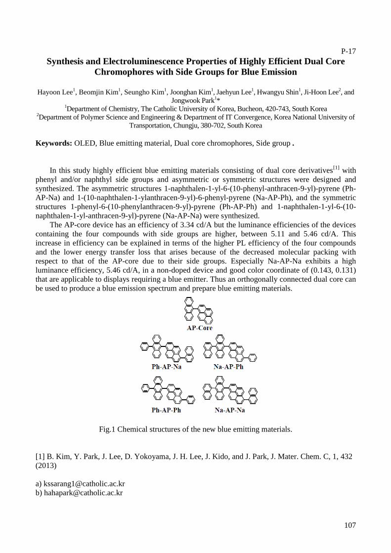
107
P-17
Synthesis and Electroluminescence Properties of Highly Efficient Dual Core
Chromophores with Side Groups for Blue Emission
Hayoon Lee1, Beomjin Kim
1, Seungho Kim
1, Joonghan Kim
1, Jaehyun Lee
1, Hwangyu Shin
1, Ji-Hoon Lee
2, and
Jongwook Park1*
1Department of Chemistry, The Catholic University of Korea, Bucheon, 420-743, South Korea
2Department of Polymer Science and Engineering & Department of IT Convergence, Korea National University of
Transportation, Chungju, 380-702, South Korea
Keywords: OLED, Blue emitting material, Dual core chromophores, Side group .
In this study highly efficient blue emitting materials consisting of dual core derivatives[1]
with
phenyl and/or naphthyl side groups and asymmetric or symmetric structures were designed and
synthesized. The asymmetric structures 1-naphthalen-1-yl-6-(10-phenyl-anthracen-9-yl)-pyrene (Ph-
AP-Na) and 1-(10-naphthalen-1-ylanthracen-9-yl)-6-phenyl-pyrene (Na-AP-Ph), and the symmetric
structures 1-phenyl-6-(10-phenylanthracen-9-yl)-pyrene (Ph-AP-Ph) and 1-naphthalen-1-yl-6-(10-
naphthalen-1-yl-anthracen-9-yl)-pyrene (Na-AP-Na) were synthesized.
The AP-core device has an efficiency of 3.34 cd/A but the luminance efficiencies of the devices
containing the four compounds with side groups are higher, between 5.11 and 5.46 cd/A. This
increase in efficiency can be explained in terms of the higher PL efficiency of the four compounds
and the lower energy transfer loss that arises because of the decreased molecular packing with
respect to that of the AP-core due to their side groups. Especially Na-AP-Na exhibits a high
luminance efficiency, 5.46 cd/A, in a non-doped device and good color coordinate of (0.143, 0.131)
that are applicable to displays requiring a blue emitter. Thus an orthogonally connected dual core can
be used to produce a blue emission spectrum and prepare blue emitting materials.
Fig.1 Chemical structures of the new blue emitting materials.
[1] B. Kim, Y. Park, J. Lee, D. Yokoyama, J. H. Lee, J. Kido, and J. Park, J. Mater. Chem. C, 1, 432
(2013)
108
P-18
Study of Charge-transfer Complexes and the Application to Organic
Optoelectronics
Hin-Wai Mo1,a)
, Ming-Fai Lo1)
, Tsz-Wai Ng1)
, Chun-Sing Lee1,b)
1Center of Super-Diamond and Advanced Films (COSDAF) and Department of Physics and
Materials Sciences, City University of Hong Kong, Hong Kong, China
Keywords: multi-layer, conductivity, charge-transfer complexes
Charge transfer and interactions at organic heterojunctions (OHJs) are known to have
influences on various properties of organic electronic devices. First of all, recent studies of near
infrared (NIR) organic photovoltaic devices (OPVs) by using charge-transfer complexes (CTCs) are
summarized. Devices with photovoltaic respond from 900 nm to 1500 nm are demonstrated. The
new IR absorption band is attributed to the charge-transfer complex formed by electron transfer
between the donor and acceptor upon intimate contact.
In addition, high electric conductivity is observed in multilayer stack of m-MTDATA /
F16CuPc. Impedance data shows that the circuit resistance is significantly dropped by three orders of
magnitude from around 0.2 MΩ to around 0.4 kΩ when the number of alternating units is increased
from one to six, keeping a total thickness of 300 nm. Impedance results show that as the number of
alternating units increases, the organic stack shows an increasing capacitance and a decreasing
resistance. This result suggests the increasing charges accumulate at the heterojunctions, leading to
reduction in overall film resistance. The application of the high conductive units in OLED device
results in stability enhancement.
109
P-19
Alkoxyphenyl-Substituted Indacenodithiophenyl/Isomer Donor Unit for
Efficient Bulk Heterojunction Solar Cells
Hongyan Huang1, Shuli Liu
1, Baomin Zhao
1,a), Wei Huang
2,b)
1Institute of Advanced Materials (IAM); Nanjing University of Posts and Telecommunications,
9 Wenyuan Road, Nanjing 210046, P. R. China, 2Jiangsu-Singapore Joint Research Center for
Organic/Bio-Electronics &Information Displays and Institute of Advanced Materials, Nanjing
University of Technology, Nanjing 210003, P. R. China Keywords: solar cells, bulk heterojunction, low band gap, D-A copolymers, indacenodithiophene
Bulk heterojunction (BHJ) polymer solar cells (PSCs) have attracted much attention over the
past two decades owing to their unique advantages, such as low manufacturing cost, easy fabrication,
light weight characteristics, and device structural flexibility. So far, single-junction PSCs have
exceeded 9% PCE. Through prolonged effort, many low-band-gap conjugated polymers have been
designed and synthesized with the aim of improving charge transporting properties, narrowing the
band gap to harvest more sunlight and deepening the highest occupied molecular orbital (HOMO)
energy level in order to increase the open circuit voltage (Voc). Among them, indacenodithiophene
(IDT) based D-A copolymers have been developed and exhibit promising photovoltaic performance
due to that rigid and extended conjugated structure of IDT can effectively enhance interchain
interaction of the polymers and improve charge carrier mobility higher hole mobility.
In this work, two new D-A copolymers containing IDT/isomer donor unit and DTBT acceptor
unit PIDT2DTBT and PIDT3DTBT, were synthesized to study their structure-property relationships
for the application in PSCs. The two copolymers show narrow bandgap and broad absorption in the
visible region. Under the illumination of AM 1.5G, 100 mW/cm2, the PSC based on
PIDT2DTBT/PC71BM demonstrated a power conversion efficiency of 5.38%, which is significantly
improved in comparison with that 2.29% of the device based on PIDT3DTBT /PC71BM under the
same experimental conditions.
Reference:
[1] He, Z. C.; Zhong, C. M.; Su, S. J.; Xu, M.; Wu, H. B.; Cao, Y. Nat. Photon. 2012, 6, 591−595.
[2] Chen, C.-P.; Chan, S.-H.; Chao, T.-C.; Ting, C.; Ko, B.-T. J. Am. Chem. Soc.2008, 130, 12828.
[3] Zhang, Y.; Zou, J.; Yip, H.-L.; Chen, K.-S.; Zeigler, D. F.;Sun, Y.; Jen, A. K. Y. Chem.
Mater.2011, 23, 2289–2291.
[4] Zhang, M. J.; Guo, X.; Wang, X. C.; Wang, H. Q.; Li, Y. F. Chem.Mater.2011, 23, 4264.
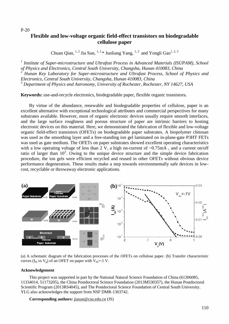
110
P-20
Flexible and low-voltage organic field-effect transistors on biodegradable
cellulose paper
Chuan Qian, 1, 2
Jia Sun, 1, 2
* Junliang Yang, 1, 2
and Yongli Gao1, 2, 3
1 Institute of Super-microstructure and Ultrafast Process in Advanced Materials (ISUPAM), School
of Physics and Electronics, Central South University, Changsha, Hunan 410083, China 2 Hunan Key Laboratory for Super-microstructure and Ultrafast Process, School of Physics and
Electronics, Central South University, Changsha, Hunan 410083, China 3 Department of Physics and Astronomy, University of Rochester, Rochester, NY 14627, USA
Keywords: use-and-recycle electronics, biodegradable paper, flexible organic transistors.
By virtue of the abundance, renewable and biodegradable properties of cellulose, paper is an
excellent alternative with exceptional technological attributes and commercial perspectives for many
substrates available. However, most of organic electronic devices usually require smooth interfaces,
and the large surface roughness and porous structure of paper are intrinsic barriers to hosting
electronic devices on this material. Here, we demonstrated the fabrication of flexible and low-voltage
organic field-effect transistors (OFETs) on biodegradable paper substrates. A biopolymer chitosan
was used as the smoothing layer and a free-standing ion gel laminated on in-plane-gate P3HT FETs
was used as gate medium. The OFETs on paper substrates showed excellent operating characteristics
with a low operating voltage of less than 2 V, a high on-current of ~0.75mA , and a current on/off
ratio of larger than 103. Owing to the unique device structure and the simple device fabrication
procedure, the ion gels were efficient recycled and reused in other OFETs without obvious device
performance degeneration. These results make a step towards environmentally safe devices in low-
cost, recyclable or throwaway electronic applications.
(a) A schematic diagram of the fabrication processes of the OFETs on cellulose paper. (b) Transfer characteristic
curves (Ids vs Vg) of an OFET on paper with Vds=-1 V.
Acknowledgement
This project was supported in part by the National Natural Science Foundation of China (61306085,
11334014, 51173205), the China Postdoctoral Science Foundation (2013M530357), the Hunan Postdoctoral
Scientific Program (2013RS4045), and The Postdoctoral Science Foundation of Central South University.
YLG also acknowledges the support from NSF DMR-1303742.
Corresponding authors: [email protected] (JS)
(a) (b)

111
P-21
Surface Mechanical Attrition Treatment (SMAT)-Facilitated Fabrication of
Porous Cu for Superior 3D Monolithic Supercapacitor Electrodes
Jie Zhang 1,2,3,a)
, Yangyang Li1,2,b*)
, Jian Lu 3,c*)
1 Center of Super-Diamond and Advanced Films (COSDAF), City University of Hong Kong, 83 Tat Chee
Avenue, Kowloon, Hong Kong 2 Department of Mechanical and Biomedical Engineering, City University of Hong Kong, 83 Tat Chee
Avenue, Kowloon, Hong Kong 3 Department of Physics and Materials Science, City University of Hong Kong, 83 Tat Chee Avenue,
Kowloon, Hong Kong
Keywords: SMAT, chemical dealloying, Cu alloys, porous metals, supercapacitors
Abstract:
A facile approach is developed to mass produce porous 3-D bulk metallic nanostructure with high
purity, fine nanostructures of high specific surface area, and improved mechanical performance, at a
low cost and high production rate. This approach is based on an effective mechanical pretreatment
method (surface mechanical attrition techniques, SMAT) and the convenient dealloying technique. It
was found that this novel approach is able to effectively remove the reactive metal at an accelerated
rate, and greatly improve the morphology of the porous metallic framework, leading to 3-D bulk
nanoporous structures. The porous Cu-based nanostructures obtained using this method showed
superior performance for supercapacitor electrodes.
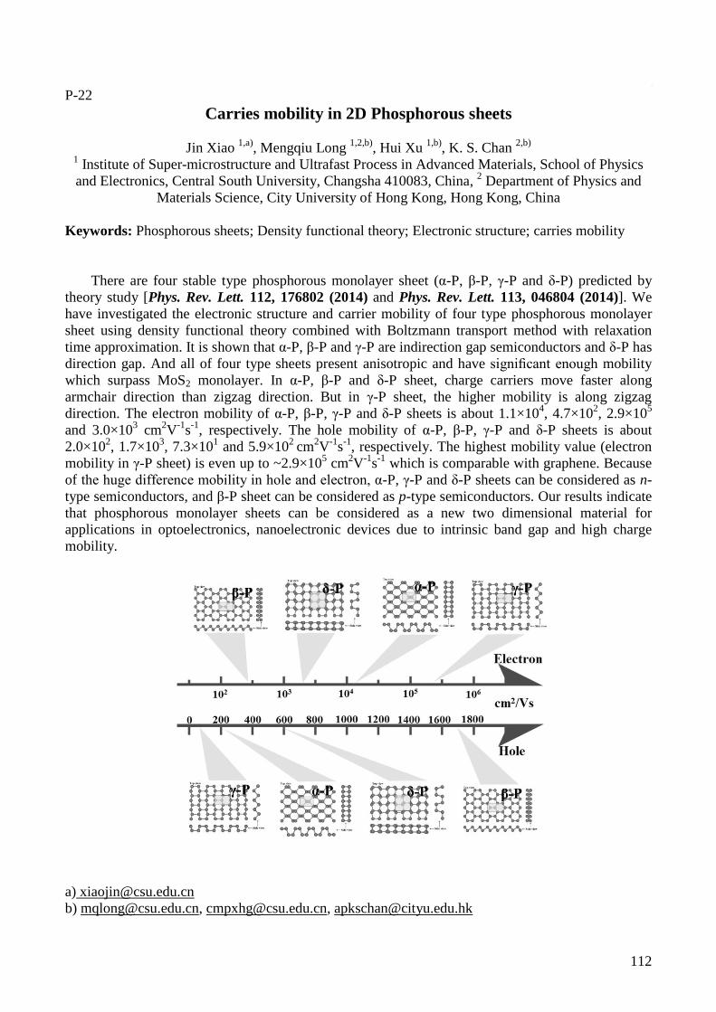
112
2 P-22
Carries mobility in 2D Phosphorous sheets
Jin Xiao 1,a)
, Mengqiu Long 1,2,b)
, Hui Xu 1,b)
, K. S. Chan 2,b)
1 Institute of Super-microstructure and Ultrafast Process in Advanced Materials, School of Physics
and Electronics, Central South University, Changsha 410083, China, 2 Department of Physics and
Materials Science, City University of Hong Kong, Hong Kong, China
Keywords: Phosphorous sheets; Density functional theory; Electronic structure; carries mobility
There are four stable type phosphorous monolayer sheet (α-P, β-P, γ-P and δ-P) predicted by
theory study [Phys. Rev. Lett. 112, 176802 (2014) and Phys. Rev. Lett. 113, 046804 (2014)]. We
have investigated the electronic structure and carrier mobility of four type phosphorous monolayer
sheet using density functional theory combined with Boltzmann transport method with relaxation
time approximation. It is shown that α-P, β-P and γ-P are indirection gap semiconductors and δ-P has
direction gap. And all of four type sheets present anisotropic and have significant enough mobility
which surpass MoS2 monolayer. In α-P, β-P and δ-P sheet, charge carriers move faster along
armchair direction than zigzag direction. But in γ-P sheet, the higher mobility is along zigzag
direction. The electron mobility of α-P, β-P, γ-P and δ-P sheets is about 1.1×10⁴, 4.7×10
2, 2.9×10
5
and 3.0×103 cm
2V
-1s
-1, respectively. The hole mobility of α-P, β-P, γ-P and δ-P sheets is about
2.0×10², 1.7×10
3, 7.3×10
1 and 5.9×10
2 cm
2V
-1s
-1, respectively. The highest mobility value (electron
mobility in γ-P sheet) is even up to ~2.9×105 cm
2V
-1s
-1 which is comparable with graphene. Because
of the huge difference mobility in hole and electron, α-P, γ-P and δ-P sheets can be considered as n-
type semiconductors, and β-P sheet can be considered as p-type semiconductors. Our results indicate
that phosphorous monolayer sheets can be considered as a new two dimensional material for
applications in optoelectronics, nanoelectronic devices due to intrinsic band gap and high charge
mobility.

113
P-23
A Supramolecular π-Stacked Conjugated Polymer: Preventing Interchain π-π
Stacking toward Deep Blue Polymer Light-emitting Diode and Laser
Jinyi Lin,1,2,a)
Bin Liu,2 Linghai Xie,*
2,b) Ruidong Xia
2 and Wei Huang*
1,2,b)
1Full address of first author, including country,
2List all distinct addresses in the same way
Key Laboratory of Flexible Electronics (KLOFE) & Institute of Advanced Materials (IAM), National Synergistic
Innovation Center for Advanced Materials (SICAM), Nanjing Tech University (NanjingTech), 30 South Puzhu Road,
Nanjing 211816, P. R. China. 2Key Laboratory for Organic Electronics and Information Displays & Institute of Advanced Materials(IAM), National
Synergistic Innovation Center for Advanced Materials (SICAM), Nanjing University of Posts & Telecommunications, 9
Wenyuan Road, Nanjing 210023, P. R. China
Keywords: Supramolecular π-Stacked Conjugated Polymer, Single-chain Behavior, Supramolecular
Conjugated Polymer Nanowires, Excellent Spectral Stability, Optoelectronic Device
For the large packing density and short inter-chain distance in conjugated polymer films, interchain π-π
interactions of backbone chain can result into a wide variety of rather complex inter- or intrachain photo-
physical processes, such as energy transfer, self-absorption, and excimer formation.1 For the light-emitting
conjugated polymer (LCP), interchain aggregation may lead to reduce photoluminescence quantum yield
(PLQY) and energy gap, lower color purity and spectral stability.2 These are undesirable, especially for
fabrication of deep polymer blue-emitting devices (PLEDs). For the pervasive conformational and energetic
disorder, an effective strategy for attaining stable deep blue emissive polymer films is to isolate the backbone
chain, inhibit inter-chain interactions and further suppress aggregation.3 Herein, we first proposed that the
supramolecular π-stacked conjugated polymer (SSCPs) was an effective candidate to prevent interchain π-π
stacking interaction, that the stacked units in the side chain can play as a block layer to suppress molecular
aggregate and improve their spectral stability. Therefore, we introduced the carbazole (Cz) group as a pendent
stacked unit into polydiarylfluorenes to fabricate a novel SSCPs, PCzODPF, as a model to investigate the
effect of Cz stacked interaction on the molecular aggregation and opto-electrical property. PCzODPF
exhibited intrachain absorption and emission behavior (single chain photo-physical processing) in solution,
gel and film states. Moreover, PCzODPF films showed excellent spectral stability without the notorious green
emission under thermal annealing at 200 °C or aging 21 days in the ambient atmosphere, indicating that the
stacked Cz groups may act as a blocking layer to effective inhibit inter-chain aggregation (Figure 1). Weaker
inter-chain interaction enabled single layer PLEDs with stable single chain deep blue emission, and higher
current efficiency (C. E.) and lower turn on voltages than in control polymers (2.54 cd A-1
and 3.9 V
respectively). PCzODPF also exhibits notable properties as active gain medium for polymer lasers (468 nm),
leading to low lasing threshold values.
Figure 1. Schematic diagram illustrating the molecular packing model of PCzODPF and their spectra
1 L. Xie, C. Yin, W. Lai, Q. Fan, W. Huang, Prog. Polym. Sci. 2012, 37, 1192.
2 J. Lin, Z. Yu, W. Zhu, G. Xing, Z. Lin, S. Yang, L. Xie, C. Niu, W. Huang, Polym. Chem. 2013, 4, 477.
3 J. Lin, W. Zhu, F. Liu, L. Xie, L. Zhang, R. Xia, G. Xing, W. Huang, Macromolecules 2014, 47, 1001.
a) [email protected] (J-Y. L.)
b) [email protected] (W. H.); [email protected] (L-H. X)

114
P-24
GO Based Quaternary States Memory
Lai-yuan Wang,
1,a) Ming-dong Yi,
1 Ling-hai Xie,
1 Wei Huang*
1,2,b)
1 National Synergistic Innovation Center for Advanced Materials (SICAM), Key Laboratory for Organic
Electronics & Information Displays (KLOEID), Jiangsu-Singapore Joint Research Center for Organic/Bio
Electronics & Information Displays, and Institute of Advanced Materials (IAM),
Nanjing University of Posts &Telecommunications, Nanjing 210023, China
2 National Synergistic Innovation Center for Advanced Materials (SICAM), Key Laboratory of Flexible
Electronics (KLOFE), Jiangsu-Singapore Joint Research Center for Organic/Bio Electronics & Information
Displays, and Institute of Advanced Materials (IAM), Nanjing Tech University, Nanjing 211816, China
E-mail: a) [email protected], b) [email protected] / [email protected]
Keywords: memory, GO, quaternary states, oxygen-migration
Increasing the number of state in each elemental cell is an effective method to increasing the
data storage, and it paves a new way for the development of memory devices. We report a resistive
switching device with four intrinsic states in ITO/GO/Al planar structure with GO synthesized by a
modified Hummer’s method characterized by oxidation twice combined with highly effective
centrifugation. The GO film is prepared on an ITO glass substrate by spin-coating the homogenous
solution followed by evaporating Al electrode. Electrical characterizations demonstrate it a
quaternary WORM device with fine retention performance. During the first sweep, we can observe
three states. Moreover, we obtain an additional stable state during the second sweeping cycle.
Although the ratios are not large, the four states in GO memory device distinctly exist. We attributed
them to different degrees of oxygen-migration and variable content of oxygen in the GO layer
closely dependent on the cycle number.
-6 -4 -2 0 2 4 6
1E-7
1E-5
1E-3
0.1
state4
state3
state2
Cu
rre
nt(
A)
Voltage(V)
sweep1
sweep2
sweep3
sweep4
sweep5
sweep6
state1
0 2000 4000 6000 8000 10000
10-6
10-5
10-4
10-3
10-2
10-1
Number of pulse
Curr
ent(
A)
state1
state2
state3
state4
@-1V
Fig. 1. Schematic illustration of ITO/GO/Al memory device (a) and TEM images (b) of GO film. I-V
curves of six sweeps during -6V~6V (c) and retention characteristic (d) of each state read at -1V,
corresponding to (c).
(a)
(c) (d)
(b)
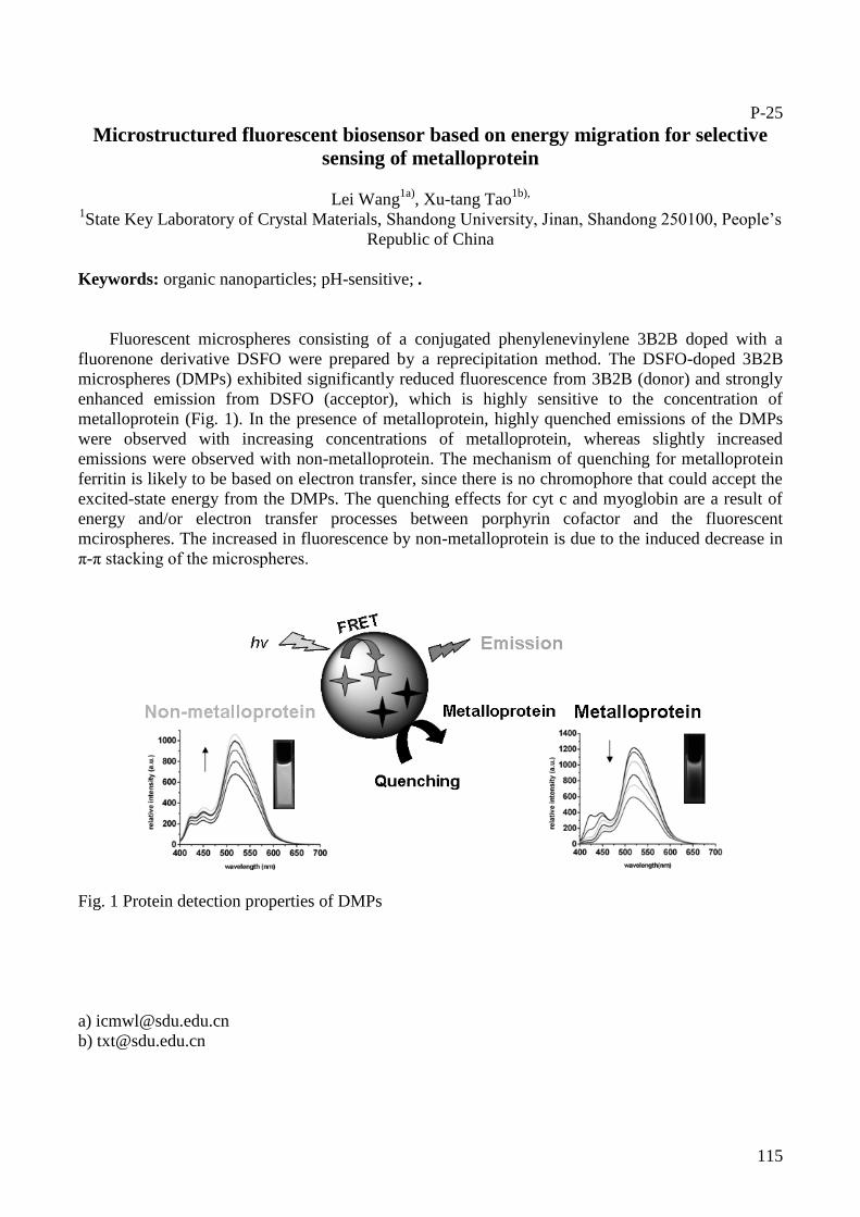
115
P-25
Microstructured fluorescent biosensor based on energy migration for selective
sensing of metalloprotein
Lei Wang1a)
, Xu-tang Tao1b),
1State Key Laboratory of Crystal Materials, Shandong University, Jinan, Shandong 250100, People’s
Republic of China
Keywords: organic nanoparticles; pH-sensitive; .
Fluorescent microspheres consisting of a conjugated phenylenevinylene 3B2B doped with a
fluorenone derivative DSFO were prepared by a reprecipitation method. The DSFO-doped 3B2B
microspheres (DMPs) exhibited significantly reduced fluorescence from 3B2B (donor) and strongly
enhanced emission from DSFO (acceptor), which is highly sensitive to the concentration of
metalloprotein (Fig. 1). In the presence of metalloprotein, highly quenched emissions of the DMPs
were observed with increasing concentrations of metalloprotein, whereas slightly increased
emissions were observed with non-metalloprotein. The mechanism of quenching for metalloprotein
ferritin is likely to be based on electron transfer, since there is no chromophore that could accept the
excited-state energy from the DMPs. The quenching effects for cyt c and myoglobin are a result of
energy and/or electron transfer processes between porphyrin cofactor and the fluorescent
mcirospheres. The increased in fluorescence by non-metalloprotein is due to the induced decrease in
π-π stacking of the microspheres.
Fig. 1 Protein detection properties of DMPs

116
P-26
Efficient Photo flux Manipulation for Organic Light-emitting diodes Using Bio-
inspired Moth’s Eye Nanostructures
Lei Zhou1,a)
, Qingdong Ou1, Hengyang Xiang
1, Yanqing Li
1, Jianxin Tang
1,b),
1 Institute of Functional Nano & Soft Materials (FUNSOM), Soochow University, 199 Ren-Ai Road, Suzhou,
215123, China
Keywords: Organic light-emitting devices, moth eye, light out-coupling, photo flux
Organic light-emitting devices (OLEDs) have been attractive in the last two decades as next-generation
lighting source and full-color display panels. However, in conventional OLEDs constructed in a standard
substrate emitting architecture, the out-coupling efficiency is approximately 20%, and the majority of the
photo flux generated in the organic layers is confined in the devices. Here we propose a universal method of
efficient photo flux manipulation by introducing bio-inspired moth’s eye nanostructure into OLEDs both on
ITO-glass substrates and plastic with embedded Ag networks (PEANs). For OLEDs based on ITO-glass
substrate, light out-coupling efficiency of OLEDs with stacked triple emission units is over 2 times that of a
conventional device, resulting in drastic increase in external quantum efficiency and current efficiency to
119.7% and 366 cd A-1
at a luminance of 1,000 cd m-2
without introducing spectral distortion and
directionality. Furthermore, an efficient white OLED device structure is demonstrated, yielding an efficiency
exceeding 123 lm W-1
through the combination of optimum light out-coupling and energy-efficient photon
generation. Similarly, the flexible white OLEDs exhibit a maximum external quantum efficiency (EQE) of
49% and a record PE of 106 lm W-1
at 1,000 cd m-2
with angular color stability. These amazing results
represent an exciting step towards the realization of high-efficiency OLEDs for use in a wide variety of high-
performance displays and general lighting applications.
Fig. 1 Photography of flexible WOLEDs and performance characteristics of WOLEDs based on ITO-glass
and PEANs substrates.
References 1.L. Zhou, Q. D. Ou, J. D. Chen, S. Shen, J. X. Tang,* Y. Q. Li, S. T. Lee, Scientific Reports, 2014, 4, 4040.
2.D. Ou, L. Zhou, Y. Q. Li, S. Shen, J. D. Chen, C. Li, Q. K. Wang, S. T. Lee, J. X. Tang,* Advanced
Functional Materials, 2014, DOI: 10.1002/adfm.20140.
3. L. Zhou, X. C, Jiang, Y. Q. Li, J. X. Tang,* ACS applied materials & interfaces. 2014, 6, 18139− 18146
a) Email:[email protected]
b) Email: [email protected]

117
P-27
Enhanced outcoupling efficiency of white organic light emitting device
by microlens array and internal scattering layer
Mei Meng1,a)
, Byung Doo Chin2,b)
1,2
Department of Polymer Science and Engineering, Dankook University, 152, Jukjeon-ro,
Suji-gu, Yongin-si, Gyeonggi-do, 448-701, Korea
Keywords: Light outcoupling, microlens, scattering layer, white OLED.
Current approaches on the light extraction technology of OLEDs are usually limited to single-color
emission or rely on complicated, expensive equipment and process such as vacuum evaporation or
lithographic procedures. Considering practical applications, it is essential that fabrication techniques must be
applicable to a large area, multicolor (in case of white lighting), and cost effective. Hence, it is desirable to
develop a simple fabrication technique for these out-coupling structures and study its effectiveness in terms of
different colors.
In this study, solution-processed internal and external out-coupling structures for white organic light
emitting devices (WOLED) were investigated [1]. Suitable size and thickness of inside scattering layer with
nanoscale titanium dioxide (TiO2) particles were selected in combination with metal grid-polymer composite
printable anode system. Transmittance and haze, as a function of particle size and thickness of scattering
layer, were characterized. Structure of WOLED with scattering layer used in this study is Glass/SL(3µm)/
PEDOT: PSS(60nm)/Ag grid/DNTPD(50nm)/TAPC(20nm)/mCP:Firpic-10wt%(20nm)/CBP:Ir(piq)2acac-
8wt%(10nm) /Bphen(30nm)/LiF(2nm)/Al(100nm); see Fig 1. The matrix of scattering layer was negative
photoresist polymer (Ormocomp®). For the external out-coupling structure, microlens formed by convective
self-assembly patterns was employed; polystyrene latex beads (Alfa Aesar) and polymethylmethacrylate
powder (LDX30C, Sunjin chemical) were used for regular and irregular microbeads.
For WOLED internal without inside scattering layer, maximum luminous efficiency of reference device,
irregular lens device and regular lens device are 7.24cd/A, 7.85cd/A, and 8.77cd/A, while the quantum
efficiency of them are 6.56%, 7.11%, and 7.96%. For scattering layer (350nm TiO2)-containing WOLED,
maximum luminous efficiency of reference device, irregular lens device and regular lens device are
11.98cd/A, 12.00cd/A and 13.38cd/A. Corresponding quantum efficiency of them are 9.88%, 9.92%, and
10.95%, respectively. It is probed that combination of internal scattering layer and external microlens were
more effective for enhancement of light outcoupling, while the overall factors of increase is not great. Usually,
microlens plays a role as extracting waveguide mode emission at interface between substrate and air, however,
internal scattering layer can extract light from transparent electrode to glass. Due to the broadband light
emitting spectrum behavior of WOLED in this study, expectation for degree of light extraction at each
specific mode (glass-air, near anode, and surface plasmon effects) is complicated. Analysis on the
experimental results with proper optical simulation methods are performed and will be presented.
Fig.1 Structure of WOLED Fig.2 EQE of WOLED without scattering layer Fig.3 EQE of WOLED with scattering layer
Reference
[1] W. J. Hyun, S. H. Im, O. O Park, B. D. Chin, Org. Elect. 13, 579 (2012)

118
P-28
High-frequency oscillator based on a graphene resonant tunnelling transistor
M. J. Zhu1,a)
, J. S. Tu2, K. S. Novoselov
1, A. K. Geim
1,2, A. Mishchenko
1,b)
1School of Physics and Astronomy, University of Manchester, Oxford Road, Manchester M13 9PL, UK
2Centre for Mesoscience and Nanotechnology, University of Manchester, Manchester M13 9PL, UK
Keywords: graphene, resonant tunnelling, negative differential conductance, oscillator, THz
The use of graphene as electrodes and utilizing insulating or semiconducting materials as the
tunnelling barrier led to the creation of tunnelling transistors and tunnelling photovoltaic devices.
The combination of a hexagonal boron nitride (hBN) barrier sandwiched between two graphene
electrodes is particularly attractive, because of the exceptional crystalline quality and the small lattice
mismatch (1.8%) of two materials. An unprecedented degree of controlling the electronic properties
of graphene-based heterostructure is not only available by means of the selection of materials in the
stack, but also through the additional relative orientation of the component layers.
Here we report a new series of tunnelling transistor in which the crystal lattice of two graphene
layers are intentionally aligned to a high degree of precision (<2o) during the fabrication procedure
1.
Our measurement and theoretical modelling of the device characteristics reveal that the current flow
is dominated by tunnel transitions in which both energy and in-plane momentum are conserved. The
resonant conditions exist in a narrow range of bias voltages, and result in a resonant peak in the
current-voltage characteristics, which leads to a strong negative differential conductance (NDC) that
can persist up to room temperature. The bias position of the resonance can be controlled by relative
orientation the two graphene crystalline lattices and the external magnetic field. In the NDC region,
our devices generate radiofrequency oscillations when connected to a simple inductor-capacitor
circuit. The frequency range is mainly limited by the parasitic capacitance between the contact pads
of our devices and the underlying silicon gate. Much higher frequencies could be reached by
reducing those parasitic capacitors. Even higher frequencies could also be achieved by fabricating a
device in a slot antenna configuration, in which the slot acts as a resonator with the resonance
frequency determined by the geometry of the slot. Moreover, our tunnelling devices are free of the
fundamental limitation intrinsic to conventional double-barrier resonant tunnelling devices, namely
the relatively long carrier dwell time (picoseconds) in the quantum well as compared with the time to
transit the single barrier (femtoseconds), which suggest that potentially our tunnelling devices can be
used to operate in the THz range.
b a c
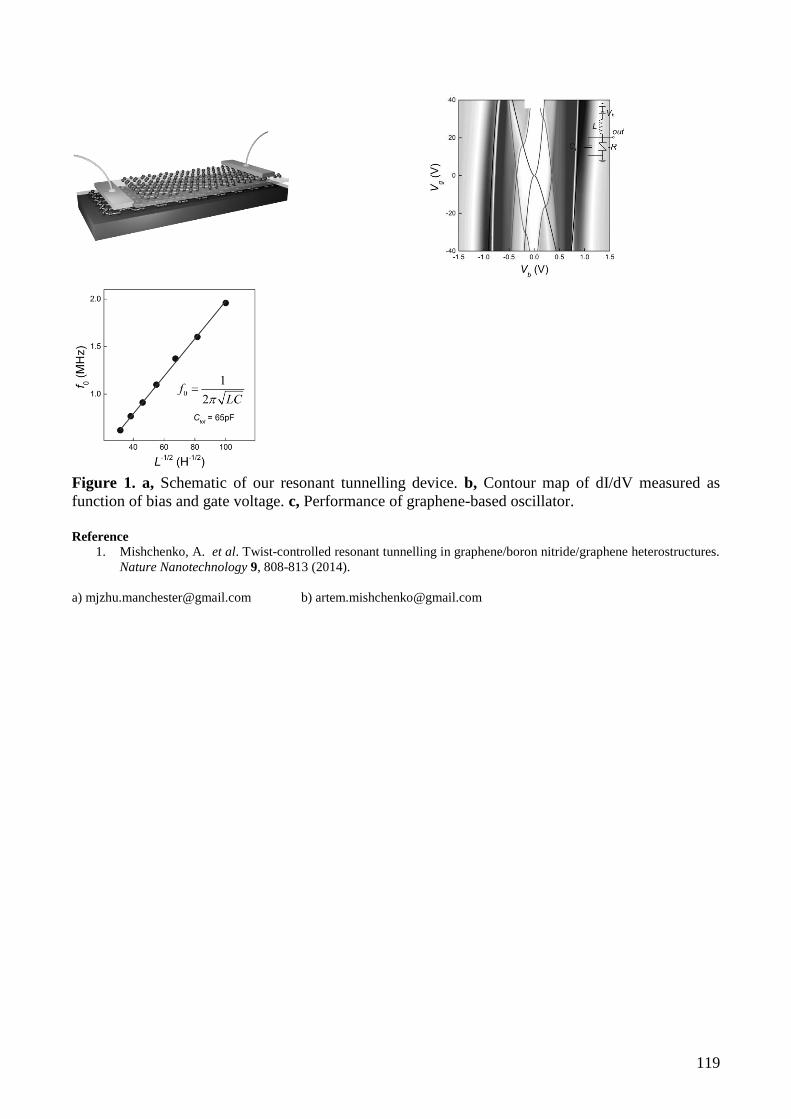
119
Figure 1. a, Schematic of our resonant tunnelling device. b, Contour map of dI/dV measured as
function of bias and gate voltage. c, Performance of graphene-based oscillator.
Reference
1. Mishchenko, A. et al. Twist-controlled resonant tunnelling in graphene/boron nitride/graphene heterostructures.
Nature Nanotechnology 9, 808-813 (2014).
120
P-29
Electronic structures and photoconversion mechanism in perovskite/fullerene
heterojunctions
Ming-Fai Loa)
, Chun-Sing Lee b)
Center of Super-Diamond and Advanced Films (COSDAF), Department of Physics and Materials
Science,
City University of Hong Kong, Hong Kong SAR, P. R. China
Keywords: Perovskite, organic heterojunction, photoemission study, fullerene
It has been generally believed and assumed that organometal halide perovskites would form
type II P-N junctions with fullerene derivatives (C60 or PCBM), and the P-N junctions would provide
driving force for exciton dissociation in perovskite-based solar cell. To the best of our knowledge,
there is so far no experiment proof on this assumption. On the other hand, whether photo-generated
excitons can intrinsically dissociate into free carrier in the perovskite without any assistance from a
P-N junction is still controversial. To address these, we directly measure the interfacial electronic
structures of a vacuum deposited perovskite/C60 and a solution processed perovskite/PCBM
junctions by ultraviolet photoelectron spectroscopy (UPS). Contrary to the common believes, both
junctions are found to be type I N-N junctions with bandgap of the perovskites embedded by that of
the fullerenes. Meanwhile, device with such a charge inert junction can still effectively functions as a
solar cell. These results give direct experimental evidence that excitons are dissociated to free
carriers in the perovskite film even without any assistance from a P-N junction.
a) Presenting author’s Email: [email protected]
b) Corresponding author’s Email: [email protected] (C.S. Lee)

121
P-30
Highly efficient fullerene/perovskite planar
heterojunction solar cells via cathode modification
with an amino-functionalized polymer interlayer
Qifan Xue, Zhicheng Hu, Fei Huang,* Hin-Lap Yip* and Yong Cao
Institute of Polymer Optoelectronic Materials and Devices, State Key Laboratory of
Luminescent Materials and Devices, South China University of Technology,
Guangzhou 510640, P. R. China
Keywords: perovskite solar cells, interfacial engineering, amino-functionalized polymer interlayer
A new amino-functionalized polymer, PN4N, was developed and applied as an efficient
interlayer to improve the cathode interface of fullerene/perovskite (CH3NH3PbIxCl3-x) planar
heterojunction solar cells. The PN4N polymer is soluble in IPA and n-BuOH, which are orthogonal
solvents to the metallohalide perovskite films, and therefore they can be spuncast on the
heterojunction layer before the deposition of the metal cathode. This simple modification of the
cathode interface showed a remarkable enhancement of power conversion efficiency (PCE) from
12.4% to 15.0% and also reduced the hysteresis of photocurrent (See fig. 1). We also found that
conventional water–methanol-soluble polymer interlayer, such as PFN, was incompatible with the
perovskite films because of the small molecular size of aprotic solvent such as MeOH, which could
decompose the perovskite films to PbI2, resulting in considerably lower solar cell performance. This
study provides new design guidelines for efficient interfacial materials and also demonstrates that
interface engineering could be a key strategy to improve perovskite solar cells.
Fig. 1 Device structure of the hybrid planar heterojunction solar cell and the molecular structure of
PN4N and PFN as well as the cell performance.
a) Presenting author’s Email: [email protected] (Qifan Xue)
b) Corresponding author’s Email: [email protected] (Hin-Lap Yip)

122
P-31
Effects of Graphene Defect on Electronic structures of Its Interface with Organic
Semiconductor
Qing-Dan Yang1, Hin-Wai Mo
1, Ming-Fai Lo
1, Tsz-Wai Ng
1*, Sai-Wing Tsang
2 and Chun-Sing
Lee1*
1 Department of Physics and Materials Science, Center of Super-Diamond and Advanced Films
(COSDAF) City University of Hong Kong, Hong Kong SAR, P. R. China
2 Department of Physics and Materials Science, City University of Hong Kong, Hong Jong SAR, P.
R. China
Keywords: Graphene, Electronic Structure, UPS, Defect.
Since the first reported in 2004,1 graphene has attracted significant attention due to its unique
properties, including outstanding electron mobility, 2-5
high mechanical strength, 6,7
and extremely
high thermal conductivity,8 etc. These fascinating properties make graphene an ideal candidate for
many applications in organic electronic devices. The quality and surface chemistry of graphene
crucially determine its performance in device applications. Various plasma treatments have been
employed to modify the physical, chemical, and electronic properties of graphene.
It is worth noting that during the plasma treatment, defects would be inevitably introduced in the
graphene. However, up till now, there are few reports on the implications of defect density in
graphene on its applications in organic electronic devices.
Electronic structures of copper hexadecafluorophthalocyanine (F16CuPc)/graphene with different
defect density were studied with ultra-violet photoelectron spectroscopy (UPS). We showed that the
charge transfer interaction and charge flow direction can be interestingly tuned by controlling the
defect density of graphene through time-controlled H2 plasma treatment. By increasing the treatment
time of H2 plasma from 30 second to 5 minutes, both the interface surface dipole and the electron
transporting barrier at F16CuPc/graphene interface are significantly reduced from 0.86 to 0.56 eV and
0.71 to 0.29 eV, respectively. These results suggested that graphene’s defect control is a simple
approach for tuning electronic properties of organic/graphene interfaces.
References
1 K. S. Novoselov, A. K. Geim, S. V. Morozov, D. Jiang, Y. Zhang, S. V. Dubonos, I. V. Grigorieva
and A. A. Firsov, Science 306, 666 (2004).
2 Z. F. Liu, Q. Liu, Y. Huang, Y. F. Ma, S. G. Yin, X. Y. Zhang, W. Sun and Y. S. Chen, Adv.
Mater. 20, 3924 (2008).
3 J. M. Yun, J. S. Yeo, J. Kim, H. G. Jeong, D. Y. Kim, Y. J. Noh, S. S. Kim, B. C. Ku and S. I. Na,
Adv. Mater. 23, 4923 (2011).
4 X. Huang, Z. Y. Zeng, Z. X. Fan, J. Q. Liu and H. Zhang, Adv. Mater. 24, 5979 (2012).
5 Y. Zhang, Y. W. Tan, H. L. Stormer and P. Kim, Nature 438, 201 (2005).
6 C. Lee, X. D. Wei, J. W. Kysar and J. Hone, Science, 321, 385 (2008).
7 S. Park and R. S. Ruoff, Nat. Nanotechnol. 4, 217 (2009).
8 A. A. Balandin, S. Ghosh, W. Z. Bao, I. Calizo, D. Teweldebrhan, F. Miao and C. N. Lau, Nano
Lett. 8, 902 (2008).
a) Presenting author’s Email: [email protected], [email protected],
[email protected], [email protected]
b) Corresponding author’s Email: [email protected], [email protected]
123
P-32
Funtional materials for organic flash memories
Su-Ting Han 1
, Ye Zhou 1, V. A. L. Roy
1
1Center of Super-Diamond and Advanced Films and Department of Physics and Materials Science,
City University of Hong Kong, Hong Kong, China
Email: [email protected]
Keywords: printed electronics, flash memory, floating gate, organic semiconductor, transistors
The next-generation electronic systems are expected to be light, flexible and portable for applications
in large area displays, integrated circuits (ICs), organic light emitting diodes (OLEDs), radio
frequency identification (RFID) tags, solar cells and so on. Memory is an essential part of advanced
electronic systems for data processing, storage and communication. Among many types of memories
such as ferroelectric, electret, resistive and floating gate, nano-floating gate flash memory devices
have gained a great deal of attention due to the simple device structure, non-destructive read-out and
controlled trap capacity. In this presentation, we will demonstrate recent works based on solution
processable or printable materials for organic flash memories.
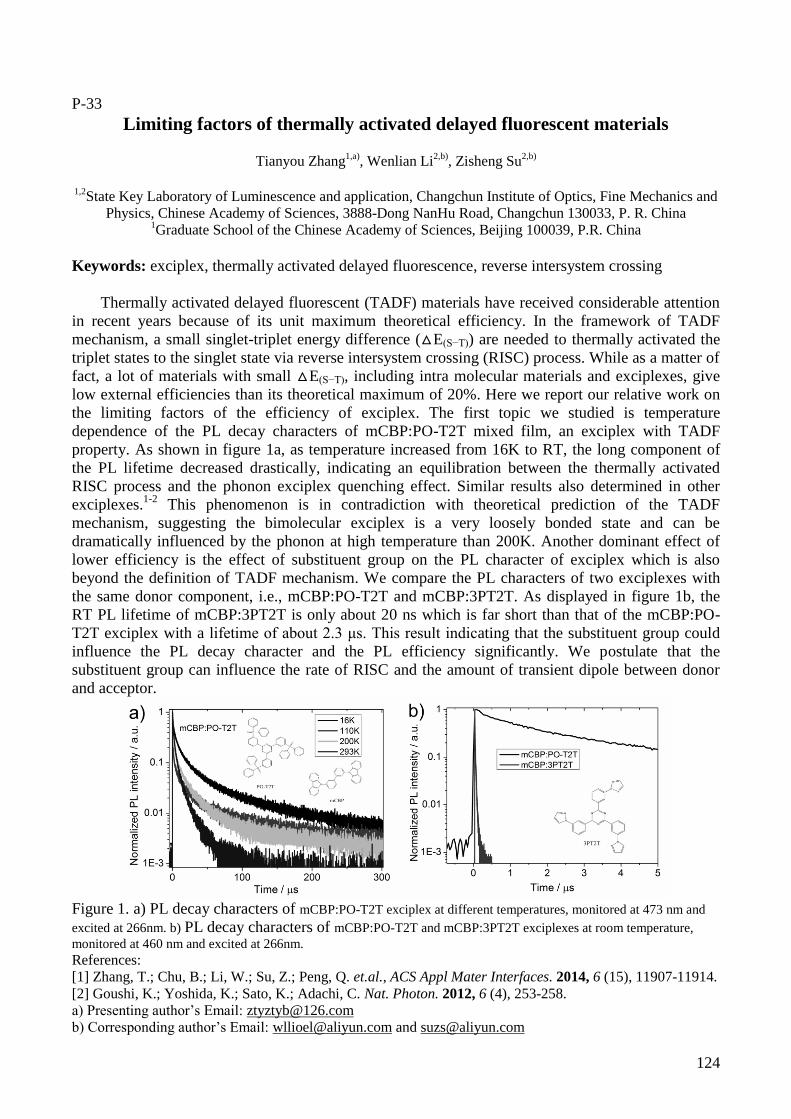
124
P-33
Limiting factors of thermally activated delayed fluorescent materials
Tianyou Zhang1,a)
, Wenlian Li2,b)
, Zisheng Su2,b)
1,2
State Key Laboratory of Luminescence and application, Changchun Institute of Optics, Fine Mechanics and
Physics, Chinese Academy of Sciences, 3888-Dong NanHu Road, Changchun 130033, P. R. China 1Graduate School of the Chinese Academy of Sciences, Beijing 100039, P.R. China
Keywords: exciplex, thermally activated delayed fluorescence, reverse intersystem crossing
Thermally activated delayed fluorescent (TADF) materials have received considerable attention
in recent years because of its unit maximum theoretical efficiency. In the framework of TADF
mechanism, a small singlet-triplet energy difference (△E(S−T)) are needed to thermally activated the
triplet states to the singlet state via reverse intersystem crossing (RISC) process. While as a matter of
fact, a lot of materials with small △E(S−T), including intra molecular materials and exciplexes, give
low external efficiencies than its theoretical maximum of 20%. Here we report our relative work on
the limiting factors of the efficiency of exciplex. The first topic we studied is temperature
dependence of the PL decay characters of mCBP:PO-T2T mixed film, an exciplex with TADF
property. As shown in figure 1a, as temperature increased from 16K to RT, the long component of
the PL lifetime decreased drastically, indicating an equilibration between the thermally activated
RISC process and the phonon exciplex quenching effect. Similar results also determined in other
exciplexes.1-2
This phenomenon is in contradiction with theoretical prediction of the TADF
mechanism, suggesting the bimolecular exciplex is a very loosely bonded state and can be
dramatically influenced by the phonon at high temperature than 200K. Another dominant effect of
lower efficiency is the effect of substituent group on the PL character of exciplex which is also
beyond the definition of TADF mechanism. We compare the PL characters of two exciplexes with
the same donor component, i.e., mCBP:PO-T2T and mCBP:3PT2T. As displayed in figure 1b, the
RT PL lifetime of mCBP:3PT2T is only about 20 ns which is far short than that of the mCBP:PO-
T2T exciplex with a lifetime of about 2.3 μs. This result indicating that the substituent group could
influence the PL decay character and the PL efficiency significantly. We postulate that the
substituent group can influence the rate of RISC and the amount of transient dipole between donor
and acceptor.
Figure 1. a) PL decay characters of mCBP:PO-T2T exciplex at different temperatures, monitored at 473 nm and
excited at 266nm. b) PL decay characters of mCBP:PO-T2T and mCBP:3PT2T exciplexes at room temperature,
monitored at 460 nm and excited at 266nm. References:
[1] Zhang, T.; Chu, B.; Li, W.; Su, Z.; Peng, Q. et.al., ACS Appl Mater Interfaces. 2014, 6 (15), 11907-11914.
[2] Goushi, K.; Yoshida, K.; Sato, K.; Adachi, C. Nat. Photon. 2012, 6 (4), 253-258.
a) Presenting author’s Email: [email protected]
b) Corresponding author’s Email: [email protected] and [email protected]

125
P-34
Formation chemistry of perovskite with mixed iodide/chloride and its
implications to charge transport properties
Tsz-Wai Ng a)
, Chun-Sing Lee b)
Center of Super-Diamond and Advanced Films (COSDAF), Department of Physics and Materials
Science,
City University of Hong Kong, Hong Kong SAR, P. R. China
Keywords: Interface energetics, XPS, formation chemistry, methylammonium iodide, lead chloride
Although Cl doping is common technique for high photovoltaic (PV) performance of
perovskite solar cells, its content is negligibly small and can be hardly tuned. We herein therefore
study the formation chemistry of Cl-doped perovskites by examining the chemical interactions
between thermally evaporated methylammonium iodide (MAI) and lead chloride (PbCl2) through X-
ray photoemission spectroscopy (XPS). We show that PbCl2 is not stable at the MAI/ PbCl2 contact
due to the difference in ionic radii of Cl- and I
- ions. The Cl atom readily detaches from the PbCl2,
which subsequently initiates electron transition from Pb to MAI. As a result, negligible amount of Cl
could be observed close to the MAI/PbCl2 contact. Via thermal-evaporation, perovskite with high
PbCl2 content can be prepared and examined. We found that metallic Pb associated with increased Cl
content can quench the photogenerated exciton in PV devices. By optimizing the ratio of MAI:PbCl2,
a perovskite solar cell with ~6% efficiency is obtained. Our result shed light on the formation
chemistry of the perovskite and its implication to charge transport properties.
a) Presenting author’s Email: [email protected]
b) Corresponding author’s Email: [email protected] (C.S. Lee)
126
P-35
Broadband Light Absorption Enhancement in Nano-structured Organic Solar
Cells
Wei-Xia LAN a)
, Yan-Xia Cui, Qing-Yi Yang, Furong Zhu b)
Department of Physics and Institute of Advanced Materials, Hong Kong Baptist University, Hong
Kong, China
Keywords: Organic photovoltaics, inverted organic solar cells, light trapping,
The broadband light absorption in nano-structured OSCs is dependent on the photonic
structures. The use of different metal nanoparticles or nanostructures, formed by cross-beam
lithography and nanoimprint techniques, has been demonstrated. Enhanced electrical losses
attenuated optical absorption was found when studying the electro-photonic optimization of OSCs
with simple optical grating structures. Here, a comprehensive study of inverted organic solar cells
(OSCs) with moth’s eye nanostructure (MEN) pattern in the active layer was carried out. The
performance of MEN-based OSCs and flat control cells, fabricated using the blend of poly[4,8-
bis[(2-ethylhexyl)oxy] benzo [1,2-b:4,5-bA] dithiophene-2,6-diyl] [3-fluoro-2-[(2-ethylhexyl)
carbonyl] thieno [3,4-b] -thiophenediyl] (PTB7):[6,6]-phenyl-C70-butyric-acid-methyl-ester
(PC70BM) was analyzed by experimental optimization and FDTD simulation. The results reveal that
nano-structured OSCs possess a 6.15 % increase in power conversion efficiencies (PCE) and a 7.24
% increase in short circuit current density (JSC) compared to a flat control OSC. The theoretical
simulation reveals that the absorption enhancement that occurs in the nanostructured active layer
contributes mainly to the improvement in cell performance.
a) Presenting author’s Email: [email protected]
b) Corresponding author’s Email: [email protected]
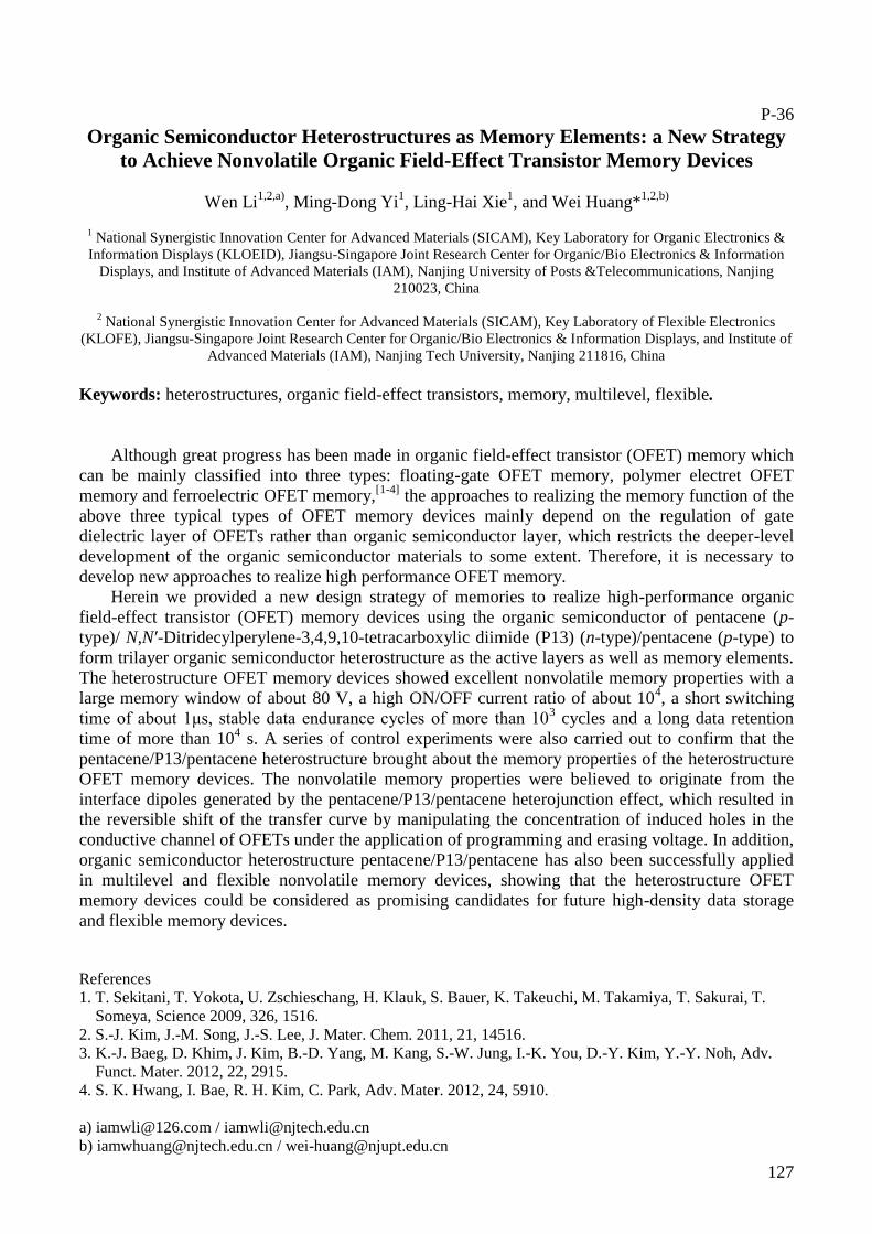
127
P-36
Organic Semiconductor Heterostructures as Memory Elements: a New Strategy
to Achieve Nonvolatile Organic Field-Effect Transistor Memory Devices
Wen Li1,2,a)
, Ming-Dong Yi1, Ling-Hai Xie
1, and Wei Huang*
1,2,b)
1 National Synergistic Innovation Center for Advanced Materials (SICAM), Key Laboratory for Organic Electronics &
Information Displays (KLOEID), Jiangsu-Singapore Joint Research Center for Organic/Bio Electronics & Information
Displays, and Institute of Advanced Materials (IAM), Nanjing University of Posts &Telecommunications, Nanjing
210023, China
2 National Synergistic Innovation Center for Advanced Materials (SICAM), Key Laboratory of Flexible Electronics
(KLOFE), Jiangsu-Singapore Joint Research Center for Organic/Bio Electronics & Information Displays, and Institute of
Advanced Materials (IAM), Nanjing Tech University, Nanjing 211816, China
Keywords: heterostructures, organic field-effect transistors, memory, multilevel, flexible.
Although great progress has been made in organic field-effect transistor (OFET) memory which
can be mainly classified into three types: floating-gate OFET memory, polymer electret OFET
memory and ferroelectric OFET memory,[1-4]
the approaches to realizing the memory function of the
above three typical types of OFET memory devices mainly depend on the regulation of gate
dielectric layer of OFETs rather than organic semiconductor layer, which restricts the deeper-level
development of the organic semiconductor materials to some extent. Therefore, it is necessary to
develop new approaches to realize high performance OFET memory.
Herein we provided a new design strategy of memories to realize high-performance organic
field-effect transistor (OFET) memory devices using the organic semiconductor of pentacene (p-
type)/ N,N′-Ditridecylperylene-3,4,9,10-tetracarboxylic diimide (P13) (n-type)/pentacene (p-type) to
form trilayer organic semiconductor heterostructure as the active layers as well as memory elements.
The heterostructure OFET memory devices showed excellent nonvolatile memory properties with a
large memory window of about 80 V, a high ON/OFF current ratio of about 104, a short switching
time of about 1μs, stable data endurance cycles of more than 103 cycles and a long data retention
time of more than 104 s. A series of control experiments were also carried out to confirm that the
pentacene/P13/pentacene heterostructure brought about the memory properties of the heterostructure
OFET memory devices. The nonvolatile memory properties were believed to originate from the
interface dipoles generated by the pentacene/P13/pentacene heterojunction effect, which resulted in
the reversible shift of the transfer curve by manipulating the concentration of induced holes in the
conductive channel of OFETs under the application of programming and erasing voltage. In addition,
organic semiconductor heterostructure pentacene/P13/pentacene has also been successfully applied
in multilevel and flexible nonvolatile memory devices, showing that the heterostructure OFET
memory devices could be considered as promising candidates for future high-density data storage
and flexible memory devices.
References
1. T. Sekitani, T. Yokota, U. Zschieschang, H. Klauk, S. Bauer, K. Takeuchi, M. Takamiya, T. Sakurai, T.
Someya, Science 2009, 326, 1516.
2. S.-J. Kim, J.-M. Song, J.-S. Lee, J. Mater. Chem. 2011, 21, 14516.
3. K.-J. Baeg, D. Khim, J. Kim, B.-D. Yang, M. Kang, S.-W. Jung, I.-K. You, D.-Y. Kim, Y.-Y. Noh, Adv.
Funct. Mater. 2012, 22, 2915.
4. S. K. Hwang, I. Bae, R. H. Kim, C. Park, Adv. Mater. 2012, 24, 5910.
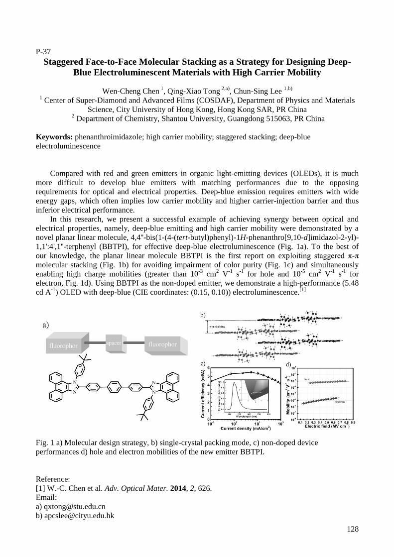
128
P-37
Staggered Face-to-Face Molecular Stacking as a Strategy for Designing Deep-
Blue Electroluminescent Materials with High Carrier Mobility
Wen-Cheng Chen 1
, Qing-Xiao Tong 2,a)
, Chun-Sing Lee 1,b)
1 Center of Super-Diamond and Advanced Films (COSDAF), Department of Physics and Materials
Science, City University of Hong Kong, Hong Kong SAR, PR China
2 Department of Chemistry, Shantou University, Guangdong 515063, PR China
Keywords: phenanthroimidazole; high carrier mobility; staggered stacking; deep-blue
electroluminescence
Compared with red and green emitters in organic light-emitting devices (OLEDs), it is much
more difficult to develop blue emitters with matching performances due to the opposing
requirements for optical and electrical properties. Deep-blue emission requires emitters with wide
energy gaps, which often implies low carrier mobility and higher carrier-injection barrier and thus
inferior electrical performance.
In this research, we present a successful example of achieving synergy between optical and
electrical properties, namely, deep-blue emitting and high carrier mobility were demonstrated by a
novel planar linear molecule, 4,4''-bis(1-(4-(tert-butyl)phenyl)-1H-phenanthro[9,10-d]imidazol-2-yl)-
1,1':4',1''-terphenyl (BBTPI), for effective deep-blue electroluminescence (Fig. 1a). To the best of
our knowledge, the planar linear molecule BBTPI is the first report on exploiting staggered π-π
molecular stacking (Fig. 1b) for avoiding impairment of color purity (Fig. 1c) and simultaneously
enabling high charge mobilities (greater than 10-3
cm2 V
-1 s
-1 for hole and 10
-5 cm
2 V
-1 s
-1 for
electron, Fig. 1d). Using BBTPI as the non-doped emitter, we demonstrate a high-performance (5.48
cd A-1
) OLED with deep-blue (CIE coordinates: (0.15, 0.10)) electroluminescence.[1]
Fig. 1 a) Molecular design strategy, b) single-crystal packing mode, c) non-doped device
performances d) hole and electron mobilities of the new emitter BBTPI.
Reference:
[1] W.-C. Chen et al. Adv. Optical Mater. 2014, 2, 626.
Email:
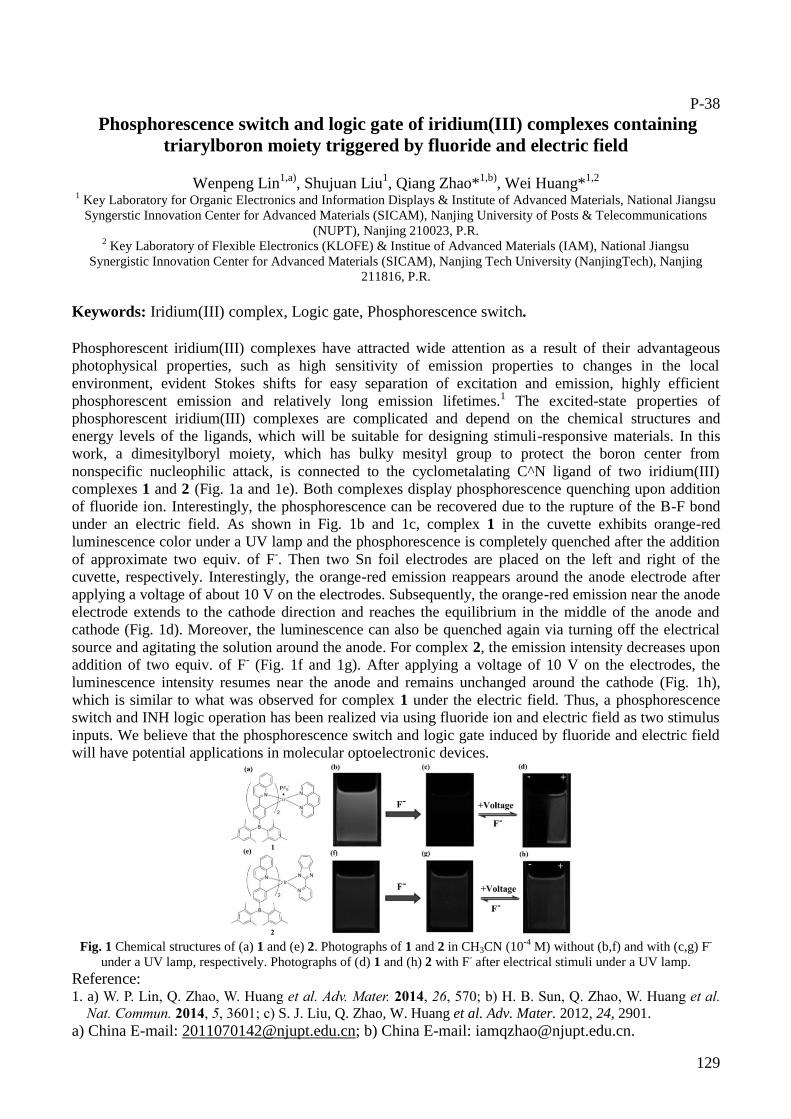
129
P-38
Phosphorescence switch and logic gate of iridium(III) complexes containing
triarylboron moiety triggered by fluoride and electric field
Wenpeng Lin1,a)
, Shujuan Liu1, Qiang Zhao*
1,b), Wei Huang*
1,2
1 Key Laboratory for Organic Electronics and Information Displays & Institute of Advanced Materials, National Jiangsu
Syngerstic Innovation Center for Advanced Materials (SICAM), Nanjing University of Posts & Telecommunications
(NUPT), Nanjing 210023, P.R. 2 Key Laboratory of Flexible Electronics (KLOFE) & Institue of Advanced Materials (IAM), National Jiangsu
Synergistic Innovation Center for Advanced Materials (SICAM), Nanjing Tech University (NanjingTech), Nanjing
211816, P.R.
Keywords: Iridium(III) complex, Logic gate, Phosphorescence switch.
Phosphorescent iridium(III) complexes have attracted wide attention as a result of their advantageous
photophysical properties, such as high sensitivity of emission properties to changes in the local
environment, evident Stokes shifts for easy separation of excitation and emission, highly efficient
phosphorescent emission and relatively long emission lifetimes.1 The excited-state properties of
phosphorescent iridium(III) complexes are complicated and depend on the chemical structures and
energy levels of the ligands, which will be suitable for designing stimuli-responsive materials. In this
work, a dimesitylboryl moiety, which has bulky mesityl group to protect the boron center from
nonspecific nucleophilic attack, is connected to the cyclometalating C^N ligand of two iridium(III)
complexes 1 and 2 (Fig. 1a and 1e). Both complexes display phosphorescence quenching upon addition
of fluoride ion. Interestingly, the phosphorescence can be recovered due to the rupture of the B-F bond
under an electric field. As shown in Fig. 1b and 1c, complex 1 in the cuvette exhibits orange-red
luminescence color under a UV lamp and the phosphorescence is completely quenched after the addition
of approximate two equiv. of F-. Then two Sn foil electrodes are placed on the left and right of the
cuvette, respectively. Interestingly, the orange-red emission reappears around the anode electrode after
applying a voltage of about 10 V on the electrodes. Subsequently, the orange-red emission near the anode
electrode extends to the cathode direction and reaches the equilibrium in the middle of the anode and
cathode (Fig. 1d). Moreover, the luminescence can also be quenched again via turning off the electrical
source and agitating the solution around the anode. For complex 2, the emission intensity decreases upon
addition of two equiv. of F- (Fig. 1f and 1g). After applying a voltage of 10 V on the electrodes, the
luminescence intensity resumes near the anode and remains unchanged around the cathode (Fig. 1h),
which is similar to what was observed for complex 1 under the electric field. Thus, a phosphorescence
switch and INH logic operation has been realized via using fluoride ion and electric field as two stimulus
inputs. We believe that the phosphorescence switch and logic gate induced by fluoride and electric field
will have potential applications in molecular optoelectronic devices.
Fig. 1 Chemical structures of (a) 1 and (e) 2. Photographs of 1 and 2 in CH3CN (10
-4 M) without (b,f) and with (c,g) F
-
under a UV lamp, respectively. Photographs of (d) 1 and (h) 2 with F- after electrical stimuli under a UV lamp.
Reference: 1. a) W. P. Lin, Q. Zhao, W. Huang et al. Adv. Mater. 2014, 26, 570; b) H. B. Sun, Q. Zhao, W. Huang et al.
Nat. Commun. 2014, 5, 3601; c) S. J. Liu, Q. Zhao, W. Huang et al. Adv. Mater. 2012, 24, 2901.
a) China E-mail: [email protected]; b) China E-mail: [email protected].

130
P-39
Electro-Mechanical Characterization of Liquid Metal and its Application on
Ionic Liquid Based Sensors
XU Shang1, 2, a)
, YIP C.K.2, LU Yang
1, 2, b)
1Department of Mechanical and Biomedical Engineering, City University of Hong Kong
2Center for Super-Diamond and Advanced Films, City University of Hong Kong
Keywords: Galinstan, flexible electronics, electro-mechanical coupling, micro-channel, sensor.
Galinstan, a eutectic metal that is composed of 68.5% Ga, 21.5% In and 10% Sn, has attracted a lot
of interests for its potential applications on flexible electronics[1]
, liquid-state sensors[2]
or batteries[3]
.
This liquid-state metal exhibits high electrical conductivity, low vapor pressure, easy phase control
properties in wide range of temperatures and is non-toxic. However, whether the rheological
behavior [4]
of the fluid liquid metal will influences the electrical conductivity when injected into
microchannel remains unclear. So, electrical and mechanical characterizations were carried out to
examine whether the fluid metal eutectic will retain its metallic conductivity in stretchable
conductive wires. In both PET and high deformable silicone tube, the resistivity of the liquid metal
increases gradually when the tube is elongated more than 300%. Detail analysis reveals that this
resistance increase because of the geometric change of the tube - the tube elongates and the cross
sectional area narrows. So further application on sensors reveals that the liquid metal can withstand
outstanding connecting functions, while another liquid, ionic liquid, can be used as the sensing
component. Specially designed micro-channel guarantees a stable heterojunction structure form at
the interface between liquid metal and ionic liquid. This kind of sensor device is highly deformable
due to the liquid-state components and the flexible PDMS substrate.
a) Presenting author: [email protected]
b) Corresponding author: [email protected]
Fig. 1. Set-up for in situ electro-mechanical characterization

131
P-40
Lifetime improvement of TADF device by using dibenzothiophene based host
materials
Wook Song1,a)
,Oh Young Kim1,
, Jun Yeob Lee1,b)
1Department of Polymer Science and Engineering, Dankook University, Suji-gu, Jukjeon-dong,
Yongin, Gyeonggi, 448-701, Korea
Keywords: OLED, TADF, Lifetime, 4CZIPN, dibenzothiophene .
We have succeed in improving the lifetime of green thermally activated delayed
fluorescence(TADF) organic light emitting device by using DBT1 and DBT2 as hosts, derived from
dibenzothiophene, and 2,4,5,6-tetra(9H-carbazol-9-yl)isophthalonitrile(4CZIPN) as a green dopant.
Quantum efficiency of device with DBT1 was 17.4% at 1000cd/A, and a maximum quantum
efficiency of 18.3% was obtained. Quantum efficiency of device with DBT2 is 17.2% at 1000cd/ m2,
and a maximum quantum efficiency of 17.5% was obtained. Two devices did not show a significant
difference, but showed better efficiency than the device using 4,4'-di(9H-carbazol-9-yl)-1,1'-
biphenyl(CBP) as host. In particular, the lifetime of the 4CZIPN device was more them doubled by
using the DBT1 and DBT2 as a host instead of common CBP. Therefore, the dibenzothiophene
derived DBT1 and DBT2 are promising as host materials to improve the efficiency and lifetime of
the 4CZIPN devices.

132
P-41
in situ controllable formation of nano-gaps for local enhancement of the
electromagnetic field
LIU Xiaowei 1, 2)
, LU Yang1, 2)
1Department of Mechanical and Biomedical Engineering, City University of Hong Kong
2Center for Super-Diamond and Advanced Films, City University of Hong Kong
Recent research indicated that nano-sized cracks can enhance the fluorescence and Raman signal for
great potential in biosensor applications. By mostly utilizing a thin layer of metal with grating
structure, we can considerably increase the electromagnetic field on the film surface once nano-gap
formed. Nanosized gaps (tens to a few hundreds of nanometers) on such metal (such as Au) thin
films have been proven to greatly increase the sensitivity, compared with just a thin layer of metal.
However, previous works usually relied on random crack formation. Here, our work mainly focuses
on the controllable, uniform gap formation on gold thin film with PDMS as the substrate. In situ
ellipsometer and Raman measurement can be used to investigate the signal enhancement from nano-
naps with specific widths, to quantify the improvement of the single molecular detection sensitivity.
Reference
[1] Bhatnagar, K., et al. "Fluorescence enhancement from nano-gap embedded plasmonic gratings by
a novel fabrication technique with HD-DVD."Nanotechnology 23.49 (2012): 495201.
[2] Anker, Jeffrey N., et al. "Biosensing with plasmonic nanosensors." Nature materials 7.6 (2008):
442-453.
[3] Nie, Shuming, and Steven R. Emory. "Probing single molecules and single nanoparticles by
surface-enhanced Raman scattering." Science 275.5303 (1997): 1102-1106.
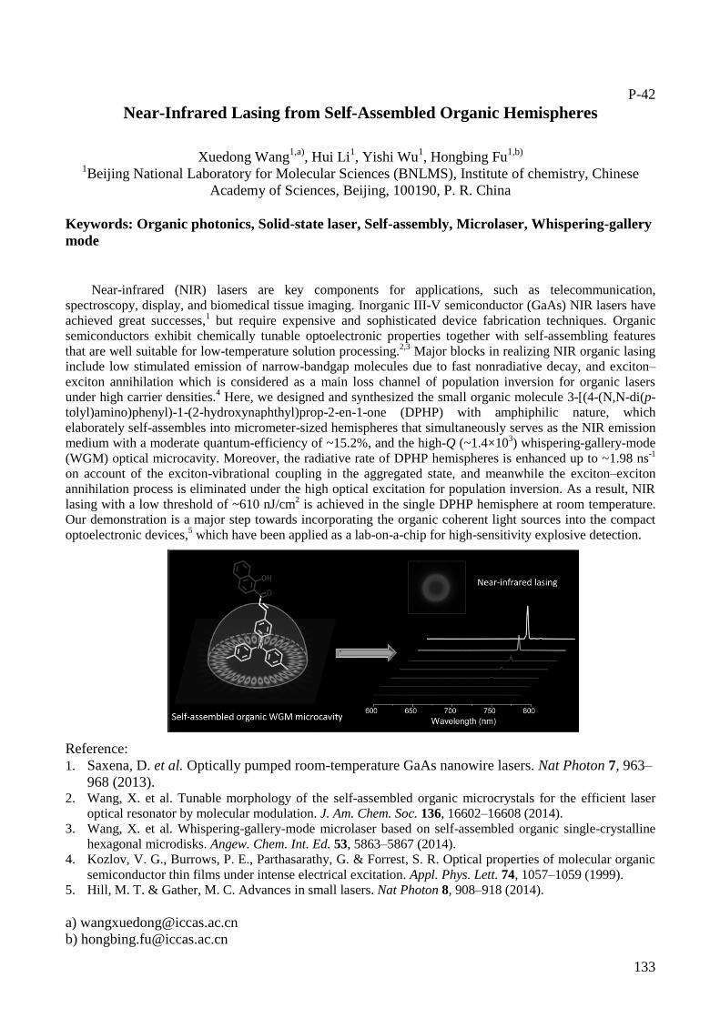
133
P-42
Near-Infrared Lasing from Self-Assembled Organic Hemispheres
Xuedong Wang1,a)
, Hui Li1, Yishi Wu
1, Hongbing Fu
1,b)
1Beijing National Laboratory for Molecular Sciences (BNLMS), Institute of chemistry, Chinese
Academy of Sciences, Beijing, 100190, P. R. China
Keywords: Organic photonics, Solid-state laser, Self-assembly, Microlaser, Whispering-gallery
mode
Near-infrared (NIR) lasers are key components for applications, such as telecommunication,
spectroscopy, display, and biomedical tissue imaging. Inorganic III-V semiconductor (GaAs) NIR lasers have
achieved great successes,1 but require expensive and sophisticated device fabrication techniques. Organic
semiconductors exhibit chemically tunable optoelectronic properties together with self-assembling features
that are well suitable for low-temperature solution processing.2,3
Major blocks in realizing NIR organic lasing
include low stimulated emission of narrow-bandgap molecules due to fast nonradiative decay, and exciton–
exciton annihilation which is considered as a main loss channel of population inversion for organic lasers
under high carrier densities.4 Here, we designed and synthesized the small organic molecule 3-[(4-(N,N-di(p-
tolyl)amino)phenyl)-1-(2-hydroxynaphthyl)prop-2-en-1-one (DPHP) with amphiphilic nature, which
elaborately self-assembles into micrometer-sized hemispheres that simultaneously serves as the NIR emission
medium with a moderate quantum-efficiency of ~15.2%, and the high-Q (~1.4×10³) whispering-gallery-mode
(WGM) optical microcavity. Moreover, the radiative rate of DPHP hemispheres is enhanced up to ~1.98 ns-1
on account of the exciton-vibrational coupling in the aggregated state, and meanwhile the exciton–exciton
annihilation process is eliminated under the high optical excitation for population inversion. As a result, NIR
lasing with a low threshold of ~610 nJ/cm2 is achieved in the single DPHP hemisphere at room temperature.
Our demonstration is a major step towards incorporating the organic coherent light sources into the compact
optoelectronic devices,5 which have been applied as a lab-on-a-chip for high-sensitivity explosive detection.
Reference:
1. Saxena, D. et al. Optically pumped room-temperature GaAs nanowire lasers. Nat Photon 7, 963–
968 (2013). 2. Wang, X. et al. Tunable morphology of the self-assembled organic microcrystals for the efficient laser
optical resonator by molecular modulation. J. Am. Chem. Soc. 136, 16602–16608 (2014).
3. Wang, X. et al. Whispering-gallery-mode microlaser based on self-assembled organic single-crystalline
hexagonal microdisks. Angew. Chem. Int. Ed. 53, 5863–5867 (2014).
4. Kozlov, V. G., Burrows, P. E., Parthasarathy, G. & Forrest, S. R. Optical properties of molecular organic
semiconductor thin films under intense electrical excitation. Appl. Phys. Lett. 74, 1057–1059 (1999).
5. Hill, M. T. & Gather, M. C. Advances in small lasers. Nat Photon 8, 908–918 (2014).
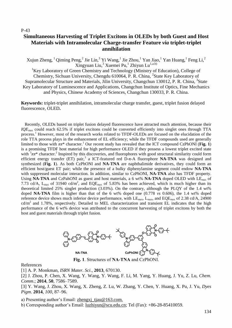
134
P-43
Simultaneous Harvesting of Triplet Excitons in OLEDs by both Guest and Host
Materials with Intramolecular Charge-transfer Feature via triplet-triplet
annihilation
Xujun Zheng, 1
Qiming Peng,2 Jie Lin,
3 Yi Wang,
1 Jie Zhou,
1 Yan Jiao,
1 Yan Huang,
1 Feng Li,
2
Xingyuan Liu,3 Xuemei Pu,
1 Zhiyun Lu
1,a.b)
1Key Laboratory of Green Chemistry and Technology (Ministry of Education), College of
Chemistry, Sichuan University, Chengdu 610064, P. R. China, 2State Key Laboratory of
Supramolecular Structure and Materials, Jilin University, Changchun 130012, P. R. China, 3State
Key Laboratory of Luminescence and Applications, Changchun Institute of Optics, Fine Mechanics
and Physics, Chinese Academy of Sciences, Changchun 130033, P. R. China.
Keywords: triplet-triplet annihilation, intramolecular charge transfer, guest, triplet fusion delayed
fluorescence, OLED.
Recently, OLEDs based on triplet fusion delayed fluorescence have attracted much attention, because their
IQEmax could reach 62.5% if triplet excitons could be converted efficiently into singlet ones through TTA
process.1 However, most of the research works related to TFDF-OLEDs are focused on the elucidation of the
role TTA process plays in the enhancement of EL efficiency; while the TFDF compounds used are generally
limited to those with ππ* character.1 Our recent study has revealed that the ICT compound CzPhONI (Fig. 1)
is a promising TFDF host material for high performance OLED if they possess a lowest triplet excited state
with 3ππ* character.
2 Inspired by this discoveries, and fluorophores with good structural similarity could form
efficient energy transfer (ET) pair,3 a ICT-featured red D-π-A fluorophore NA-TNA was designed and
synthesized (Fig. 1). As both CzPhONI and NA-TNA are naphthalimide derivatives, they could form an
efficient host/guest ET pair; while the presence of a bulky diphenylamine segment could endow NA-TNA
with suppressed molecular interaction. In addition, similar to CzPhONI, NA-TNA also has TFDF property.
Using NA-TNA and CzPahONI as guest and host materials, a 6 wt% NA-TNA doped OLED with LEmax of
7.73 cd/A, Lmax of 31940 cd/m2, and EQEmax of 5.83% has been achieved, which is much higher than its
theoretical limited 25% singlet production (3.03%). On the contrary, although the PLQY of the 1.4 wt%
doped NA-TNA film is higher than that of the 6 wt% doped one (0.778 vs 0.606), the 1.4 wt% doped
reference device shows much inferior device performance, with LEmax, Lmax, and EQEmax of 2.38 cd/A, 24900
cd/m2 and 1.78%, respectively. Detailed to MEL characterization and transient EL indicates that the high
performance of the 6 wt% device was attributed to the concurrent harvesting of triplet excitons by both the
host and guest materials through triplet fusion.
Fig. 1. Structures of NA-TNA and CzPhONI.
References
[1] A. P. Monkman, ISRN Mater. Sci., 2013, 670130.
[2] J. Zhou, P. Chen, X. Wang, Y. Wang, Y. Wang, F. Li, M. Yang, Y. Huang, J. Yu, Z. Lu, Chem.
Comm.; 2014, 50, 7586–7589.
[3] Y. Wang, J. Zhou, X. Wang, X. Zheng, Z. Lu, W. Zhang, Y. Chen, Y. Huang, X. Pu, J. Yu, Dyes
Pigm. 2014, 100, 87–96.
a) Presenting author’s Email: [email protected].
b) Corresponding author’s Email: [email protected]; Tel (Fax): +86-28-85410059.

135
P-44
Bulk Crystal Growth of organic-inorganic Perovskites CH3NH3PbX3 (X=Br, I)
Yangyang Danga)
, Xutangtaob)*
, Youxuan Sun, Haibing Xia
State Key Laboratory of Crystal Materials, Shandong University, No.27 ShandaSouth Road,
Jinan,250100,China.
Keywords: crystal growth, hybrid perovskite, CH3NH3PbX3, crystal orientations
The hybrid perovskite materials have generated significant interests due to their potential
applications in the optoelectronic fields. However, some of the fundamental properties of perovskite
materials are still disputable, because of most of them resulted from thin-film state. To better
understand the intrinsic characteristics in single crystal, here we report, for the first time, the bulk
crystal growth of CH3NH3PbX3 (MAPbX3, X=Br, I). The single crystals of cubic MAPbBr3 with
dimensions of 8 mm×8 mm×8 mm and tetragonal MAPbI3 with dimensions of 10 mm×10 mm×8 mm
were grown by temperature-lowering method in HX (X=Br, I) solution, respectively. The
orientations of MAPbX3 (X=Br, I) single crystals are conducted based on the high quality crystals.
The exhibited natural facets of MAPbBr3 were determined to be square {100} and rectangle {110},
while the exhibited natural facets of MAPbI3 were hexagon {100} and parallelogram {112} using X-
ray diffraction.
Fig. 1 The photographs of MAPbBr3 and MAPbI3 with the natural facets
136
P-45
Roughened Cu-foam coated with octahedral Cu2O for better photocatalysts
Yawen Zhan1,2,a)
, Jian Lu3, Yang Yang Li
1,2,b)
1
Center Of Super-Diamond and Advanced Films (COSDAF), City University of Hong Kong, 83 Tat
Chee Avenue, Kowloon, Hong Kong, 2 Department of Physics and Materials Science, City
University of Hong Kong, 83 Tat Chee Avenue, Kowloon, Hong Kong, 3
Department of Mechanical
and Biomedical Engineering, City University of Hong Kong, 83 Tat Chee Avenue, Kowloon, Hong
Kong
Keywords: electrodeposition, dealloying, specific surface area, foams, photocatalysts
With good thermal and electrical conductivities and good corrosion resistance, metal foams have
been widely used for electrode materials, catalysts and electromagnetic shielding materials.
However, the low surface area of commercial metal foams has largely limited their performance.
Here we report a facile electrochemical method for increasing the surface area of metal foams.
Taking Cu foams as an example, high surface area Cu foams were fabricated using this convenient
method in a one-pot one-step manner. Moreover, the treated Cu foam demonstrated significantly
improved performance for different applications, e.g., as hosts for octahedral Cu2O nanoparticles
exhibiting greatly enhanced photocatalytic performance.

137
P-46
Highly Efficient Green TADF OLED Based on Co-Host and Tandem
Architectures with External Quantum Efficiency Above 30 %
Yue-Min Xie, Liang-Sheng Liao, Man-Keung Fung*
Jiangsu Key Laboratory for Carbon-Based Functional Materials & Devices, Institute of Functional
Nano & Soft Materials (FUNSOM), Collaborative Innovation Center of Suzhou Nano Science and
Technology, Soochow University, Suzhou, Jiangsu 215123, China.
Keywords: Tandem, TADF, Green OLED
Thermally activated delayed fluorescence (TADF) based OLEDs have been attracting much attention recently
because of its high external quantum efficiency (EQE) and little efficiency roll-off. In this work, we report the
first TADF-based tandem OLED with the highest EQE achieved so far using 4CzIPN as a green TADF
emitter, mCP:TPBI as a co-host structure, and BPhen:Li/HAT-CN as a connecting unit. With the device
structure of ITO/HAT-CN (10 nm)/TAPC (40 nm)/TCTA (10nm)/mCP:TPBi:4CzIPN (1:1:0.15,
20nm)/TmPyPB (40 nm)/Bphen:Li (1.2%, 15 nm)/HAT-CN (10 nm)/TAPC (40 nm)/TCTA
(10nm)/mCP:TPBi:4CzIPN (1:1:0.15, 20nm)/TmPyPB (40 nm)/Liq (2 nm)/Al (120 nm), we successfully
fabricated green-emitting OLED with a CIE (x,y) of (0.285,0.610) and a maximum current efficiency and
EQE of 117.5 cd/A and 32.5%, respectively. The efficiency obtained in our TADF OLED is comparable to
that of phosphorescent green OLED. It was found that the co-host system has a deeper highest-occupied-
molecular-orbital (HOMO) and higher singlet and triplet energies, which eliminate exciton quenching and
provide efficient energy-transfer between the co-host and 4CzIPN.
Fig 1 (a) Current
efficiency of tandem and single-
EL-unit devices; (b) External
quantum efficiency versus current density; (c) Normalized EL spectra of tandem and
single-EL-unit devices.
0 10 20 30 400
20
40
60
80
100
120
Cu
rren
t E
ffic
ien
cy (
cd/A
)
Current Density (mA/m2)
Tandem
Single
300 400 500 600 700 800
Wavelength (nm)
0 10 20 30 400
10
20
30
40
Exte
rnal
Qu
an
tum
eff
icie
ncy
Current Density (mA/m2)
(a) (c) (b)
138
P-47
Towards highly efficient dope-free electrofluorescent materials: A fine
modulation on the components of hybridized local and charge-transfer (HLCT)
state Yulong Liu, Ping Lu*, Yuguang Ma
State Key Laboratory of Supramolecular Structure and Materials, Jilin University, Changchun,
130012 P. R. China
Keywords: Optoelectronics, PL efficiency, OLED, exciton utilization, HLCT state.
Since the first OLED was illuminated in 1987, scientists have been struggling for over two decades
for stable highly efficient organic electro-luminance, especially for the fully exciton utilization that
was once limited to 25% in terms of the spin statics. The electro-phosphorescence showed such
feasibility by directly utilizing the lowest triplet excitons for phosphorescent emission. The recently
promoted thermally activated delayed fluorescence (TADF) materials further lowered the cost of
precious metal in electrophosphorescence. However, the triplet excitons always possess long
lifetimes, which may cause serious efficiency rolling-off by triplet-triplet annihilation (TTA) and
concentrate quenching, so that the emissive layer must be doped one to avoid the problems in
OLEDs. What's more , the response time of triplet utilizing luminance is still much longer than the
fluorescence. Herein, we introduce a new concept, the hybridized local and charge-transfer (HLCT)
materials that both benefit from the high efficiency local-emissive (LE) and the small binding
charge-transfer (CT) state components, and can receive considerably stable, high efficiencies in the
electrofluorescent non-doped device by careful optimization on the molecular structure of HLCT
materials.
We designed a series of HLCT materials by an original orthogonal connection method, and carried
out systematically researches on the state species of the orthogonal HLCT molecular system. The LE
dominant material PyTPAI is high in photo luminance (PL) efficiency but is low in singlet utilization
(~12%) while the CT dominant material PyTPA-CN is low in photo luminance (PL) efficiency but is
high in singlet utilization (~80%). By carefully state modulation, the LE-enhanced material PyPTPAI
and PyPTPAI-CN relatively showed excellent electrofluorescent properties as a maximum current
efficiency of 2.69 cd/A and 3.47 cd/A, a maximum power efficiency of 2.8 lm/W and 2.1 lm/W, and
a maximum EQE of 2.9%(at 33 cd m-2
) and 2.5% (at 1786 cd m-2
) in non-doped EL device. It is an
ideal strategy to design the next-generation organic EL materials with the combined high PL
efficiency and high exciton utilization by means of HLCT state.
139
P-48
An insight on oxide interlayer in organic solar cells: From light absorption and
charge collection perspectives
Zhenghui Wu a)
, Bo Wu, Hoi Lam Tam and Furong Zhu b)
Department of Physics and Institute of Advanced Materials, Hong Kong Baptist University,
Kowloon Tong, Hong Kong
Keywords: organic solar cells, ZnO interlayer, absorption enhancement charge collection
A comprehensive study of the effect of zinc oxide (ZnO) interlayer on the performance of bulk-
heterojunction organic solar cells (OSCs), based on poly[[4,8-bis[(2-ethylhexyl)oxy] benzo [1,2-
b:4,5-b'] dithiophene-2,6- diyl] [3-fluoro-2-[(2-ethylhexyl)carbonyl] thieno [3,4-b] thiophenediyl]]
(PTB7):3'H-Cyclopropa[8,25] [5,6]fullerene-C70-D5h(6)-3'- butanoicacid, 3'-phenyl-, methyl ester
(PC70BM) blend system, is carried out by theoretical simulation and experimental optimization. It is
found that a PTB7:PC70BM blend layer thickness optimized for maximum light absorption in OSCs
does not generally give rise to the highest power conversion efficiency (PCE). The presence of a ~15
nm thick ZnO interlayer layer between a thinner photoactive layer and the cathode is favorable for
efficient OSCs. The ZnO interlayer serves a dual purpose to overcome the Optical-Electrical
Mismatch Effect as well as to reduce bimolecular charge recombination. The following three
techniques were applied to study the physical mechanisms behind the optical and electrical effects of
ZnO spacer: optical admittance analysis, measurement of light intensity dependent current-voltage
(I- V) characteristics and transient photocurrent measurements.

140
P-49
Directly observe the relaxation process of charge transfer states in organic
photovoltaics
Zhiqiang Guan1,2,a)
, Qingdan Yang1,2
, Ho Wa Li2, Jinfeng Zhang
1,2, Yuanhang Chen
2, Sai-Wing
Tsang2,b)
, Chun-Sing Lee1,2,c)
1Center of Super-Diamond and Advanced Films (COSDAF), City University of Hong Kong, Hong
Kong SAR, China
2Department of Physics and Materials Science, City University of Hong Kong, Hong Kong SAR,
China
Keywords: Organic photovoltaic, charge transfer states, relaxation process, charge modulated
electroabsorption spectroscopy
Charge transfer (CT) states formed at donor/acceptor interface determine the photocurrent
generation in organic photovoltaic (OPV) device. General models describe a competition mechanism
between the charge dissociation and energy relaxation in high-energy CT states. However, the
relaxation process is not easy to be measured due to the ultrafast charge transfer below 100 fs. In
addition, how relaxation process influences CT dissociation is still under debate.
Recently, a new technique named charge modulated electroabsorption spectroscopy (CMEAS)
was used to judge the effective bandgap of OPV. In this work, we used CMEAS to detect CT states
by sub-bandgap exciting in four polymer: fullerene OPVs, including P3HT: PC61BM, PTB7:
PC71BM, PCDTBT: PC71BM and PDTS-TPD: PC71BM. The CT signals present different response
with different modulated frequency. The signals from higher energy CT show a stable trend with
increasing frequency, just same as excitonic CMEAS signals. However, CT signals with lower
energy decrease dramatically when the frequency increases, indicating a transfer from delocalized
states to localized states. These experimental results provide the evidence for the relaxation process
from delocalized CT to localized CT. Our research suggests that with CMEAS we can directly
observe the relaxation process in CT states of OPV and by analyzing the tendency of CMEAS vs.
frequency, delocalized degree of CT states with different energy can be determined.
[1] S.-W. Tsang, S. Chen and F. So, Adv. Mater. 25, 2434 (2013).
[2] S. Chen, S.-W. Tsang, T.-H. Lai, J. R. Reynolds and F. So, Adv. Mater. 26, 6125 (2014)
a) Presenting author’s Email: [email protected]
b) Corresponding author’s Email: [email protected]
c) Corresponding author’s Email: [email protected]
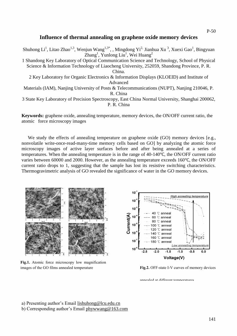
141
P-50
Influence of thermal annealing on graphene oxide memory devices
Shuhong Li
1, Litao Zhao
1,3, Wenjun Wang
1,3*, , Mingdong Yi
2, Jianhua Xu
3, Xuexi Gao
1, Bingyuan
Zhang1, Yunlong Liu
1, Wei Huang
2
1 Shandong Key Laboratory of Optical Communication Science and Technology, School of Physical
Science & Information Technology of Liaocheng University, 252059, Shandong Province, P. R.
China.
2 Key Laboratory for Organic Electronics & Information Displays (KLOEID) and Institute of
Advanced
Materials (IAM), Nanjing University of Posts & Telecommunications (NUPT), Nanjing 210046, P.
R. China
3 State Key Laboratory of Precision Spectroscopy, East China Normal University, Shanghai 200062,
P. R. China
Keywords: graphene oxide, annealing temperature, memory devices, the ON/OFF current ratio, the
atomic force microscopy images
We study the effects of annealing temperature on graphene oxide (GO) memory devices [e.g.,
nonvolatile write-once-read-many-time memory cells based on GO] by analyzing the atomic force
microscopy images of active layer surfaces before and after being annealed at a series of
temperatures. When the annealing temperature is in the range of 40-140℃, the ON/OFF current ratio
varies between 60000 and 2000. However, as the annealing temperature exceeds 160℃, the ON/OFF
current ratio drops to 1, suggesting that the sample has lost its resistive switching characteristics.
Thermogravimetric analysis of GO revealed the significance of water in the GO memory devices.
a) Presenting author’s Email [email protected]
b) Corresponding author’s Email [email protected]
Fig.1. Atomic force microscopy low magnification
images of the GO films annealed temperature Fig.2. OFF-state I-V curves of memory devices
annealed at different temperatures.

142
P-51
Highly efficient green organic light-emitting devices based on intermolecular
exciplex
Lu Zhang1,a)
, Chao Cai2, Kinlong Chan
1, Kokwai Cheah
1,2,b)
1 Department of Physics, Hong Kong Baptist University, Kowloon Tong, Hong Kong, China
2Institute of Advanced Materials, Hong Kong Baptist University, Kowloon Tong, Hong Kong, China
Keywords: OLED, exciplex
A blended bimolecular exciplex formation was demonstrated between two individual donor and
acceptor molecules, which are Tris(4-carbazoyl-9-ylphenyl)amine(TCTA) and 2,4,6-Tris(3'-(pyridin-
3-yl)biphenyl-3-yl)-1,3,5-triazine(Tm3PyBPZ). The photoluminescence of the thin film showed a
strong green exciplex emission with a peak around 514 nm, energetically identical with the energy
difference between the donor and acceptor. The photophysics study showed that this intermolecular
exciplex has a relatively high photoluminescence quantum yield, which was believed from the triplet
exciton reharvesting through the delayed fluorescence channel. By applying this exciplex as an
emitting layer, a highly efficient fluorescent organic lighting emitting diode with maximum
efficiencies of 13.1% and 53.4 lm/W can be realized with an extremely low turn-on voltage of only
2.4V.

143
P-52
A red-emissive sextuple hydrogen-bonding self-assembly molecular duplex
bearing perylene diimide fluorophores, and a white organic light-emitting diode
based on it Hui Zeng
1, Qingyu Huang
2, Jingjing Liu
1, Yan Huang
1, Suling Zhao
2, and Zhiyun Lu
1, a,b)
1 Key Laboratory of Green Chemistry and Technology of Ministry of Education, College of Chemistry, Sichuan
University, Chengdu, 610064, PR China, 2 Key Laboratory of Luminescence and Optical Information (Ministry of Education), Institute of Optoelectronics
Technology, Beijing Jiaotong University, Beijing, 100044, PR China.
Keywords: Hydrogen-Bonding Self-Assembly Duplex, Perylene Diimide, Incomplete Energy
Transfer, White Organic Light-emitting Diode
Solution-processed white organic light-emitting devices (WOLEDs) have attracted much attention owing
to their potential applications for low-cost large-area display and lighting panels, and devices based on
polymeric light-emitting materials have dominated the solution-processed WOLEDs currently. However,
polymer materials often suffer from batch-to-batch variations on molecular structures and low purity, which
are adverse to the performance and reproducibility of the devices. Compared with polymer materials,
hydrogen-bonding (HB) self-assembly supramolecules should be more promising because of their well-
defined structures, however, the electroluminescent performance of WOLEDs based on them is still
unsatisfactory.1,2
In our previous work, we have demonstrated that the introduction of sextuple HB self-assembly
oligoamide strands into small molecular fluorophores is a quite effective approach for spatial isolation of
fluorophores. Encouraged by these discoveries, herein, by incorporating red perylene diimide (PDI)
fluorophores into a sextuple HB sites, a red-emitting self-assembly supramolecular duplex PDIHB (vide Fig
1.) has been constructed successfully. Photophysical results indicate that the presence of bulky HB self-
assembly segments is beneficial to not only the suppression of concentration quenching of PDI luminogens,
but also the spatial isolation of the luminogens, hence could promote incomplete energy transfer between
PDIHB and its corresponding host material 2TPhNIHB (vide Fig. 1) reported by us before.3 Consequently,
using the doping system of PDIHB and 2TPhNIHB as the emitting layer, combined with the elctroplex
formed at the interfaces,3 a simple solution-processed two-layer WOLED with CIE coordinates of (0.42, 0.33)
has been fabricated readily. The maximum brightness and current efficiency of this WOLED are 260 cd/m2
and 0.49 cd/A, respectively; and It is worth mentioning that the chromaticity of the device is bias-independent.
All these preliminary results indicate that the HB self-assembly compounds should be promising materials in
WOLED applications. We believe that these findings are of particular interest for the development of high
performance OLEDs based on supramolecular materials.
Fig. 1. Structures of PDIHB and 2TPhNIHB
References
[1] R. Abbel, C. Grenier, M. J. Pouderoijen, J. W. Stouwdam, P. E. Leclère, R. P. Sijbesma, E. W. Meijer, A. P.
Schenning, J. Am. Chem. Soc., 2009, 131, 833-843.
[2] J. Lin, J. Wong, L. Xie, X. Dong, H. Yang, W. Huang, Macromol. Rapid Commun., 2014, 35, 895-900.
[3] J. Liu, Y. Li, Y. Wang, H. Sun, Z. Lu, H. Wu, J. Peng, Y. Huang, Opt. Mater., 2012, 34, 1535-1542.
a) Presenting author’s Email: [email protected].
b) Corresponding author’s Email: [email protected]; Tel (Fax): 86-28-85410059.

144
P-53
Novel Exciplexes for Highly Efficient OLEDs Enabled by Thermally Activated
Delayed Fluorescence (TADF)
Xiaoke Liu1,a)
, Zhan Chen2, Caijun Zheng
2, Xiaohong Zhang
3,b) and Chun-Sing Lee
1b)
1Center of Super-Diamond and Advanced Films (COSDAF) & Department of Physics and Materials
Science, City University of Hong Kong, Hong Kong SAR, P. R. China. 2Nano-organic Photoelectronic Laboratory and Key Laboratory of Photochemical Conversion and
Optoelectronic Materials, Technical Institute of Physics and Chemistry, Chinese Academy of
Sciences, Beijing 100190, P. R. China. 3Functional Nano & Soft Materials Laboratory (FUNSOM) and Collaborative Innovation Center of
Suzhou Nano Science and Technology, Soochow University, Suzhou, Jiangsu 215123, P. R. China.
Keywords: exciplex, organic light-emitting diodes, delayed fluorescence, charge-transfer (CT).
Fluorescent OLEDs based on pure TADF emitters have been reported with external quantum
efficiencies (EQE) approaching the best results of phosphorescent OLEDs. Similar to the pure TADF
emitters with intramolecular charge-transfer (CT) states, the exciplex emitters having intermolecular
CT states exhibit intrinsically small singlet-triplet energy splitting (ΔEST, ca. 0 ~ 50 meV) and allow
TADF emission via reverse intersystem crossing (RISC) from the non-radiative triplet excited state
(T1) to the radiative singlet excited state (S1). Hence, the fluorescent OLEDs based on exciplex
emitters also have theoretically 100% internal quantum efficiencies, corresponding to maximum
EQEs of 20% (assuming a typical light out-coupling efficiency of 20%). However, the EQEs of the
reported exciplex OLEDs are far lower than the theoretical limit due to the lack of exciplex emitters
with high fluorescence quantum yields (Фf). Herein, we designed three exciplexes TAPC:DPTPCz,
TCTA:DPTPCz and NPB:DPTPCz by half-and-half mixing three hole-transporting arylamines with
a high-T1 bipolar host. The three exciplexes show broad and notably red-shifted emissions relative to
those of the constituting molecules. TAPC:DPTPCz and TCTA:DPTPCz have strong TADF
emissions due to the effective energy confinement by their constituting molecules. Specially,
TAPC:DPTPCz shows high Фf of 0.68 and small ΔEST of 47 meV, affording intrinsically efficient
fluorescence radiation and high RISC efficiency. The TAPC:DPTPCz based device achieves a high
EQE of 15.4%, which is the highest performance exciplex OLED up to date. After all, high-T1
constituting molecules are shown to be preferable for designing exciplex emitters with high Фf,
because the high T1 of the constituting molecules prevent energy leakages and enable efficient RISC.
a) X.K. Liu: [email protected]
b) X.H. Zhang: [email protected]; C.-S. Lee: [email protected]
145
P-54
Interface Engineering for high-performance, low-voltage n-channel organic thin
film transistors (OTFTs) based on C60
Yaorong SU1,a)
, Weiguang XIE2,b)
, Jianbin XU1,a)
1 Department of Electronic Engineering and Materials Science and Technology Research Centre, The
Chinese University of Hong Kong, Shatin, Hong Kong SAR, China, 2 Siyuan Laboratory,
Department of Physics, Jinan University, Guangzhou, Guangdong, 510632, P. R. China.
Keywords: Interface engineering, work function, electron injection, high-performance, C60
Exploring suitable electrode materials with sufficiently low work function, ambient stability and
low-cost is of great technological importance to the development of n-channel OTFTs. Here, we
show that the work function of Cu can be effectively reduced from 4.65 eV to 4.28 eV through
surface modification via simply spin-coating a thin layer of branched polyethylenimine (PEI). By
exploiting a high-capacitance density gate dielectric (200 nF/cm2), low-voltage (3 V) C60 TFTs with
electron mobility (e) of 3.2 cm2/Vs are demonstrated with PEI modified Cu as source-drain (S/D)
electrodes. In contrast, the device with Cu S/D electrodes possesses e of only 1.0 cm2/Vs. The
improvement in electrical performance of the PEI modified device is attributed to the efficient
electron injection at the Cu/C60 interface which resulted from the reduction in work function of Cu.
Moreover, upon PEI modification, the bias stability of the device can be obviously enhanced as
compared to the unmodified one, and the resultant device exhibits an excellent thermal stability up to
200 oC without appreciable degradation in mobility. The facile modification of low-cost Cu as S/D
electrodes for high-performance n-channel OTFTs as well as the low-voltage operation will pave the
way for large scale manufacturing of organic electronics.

146
P-55
Enhanced Light Harvesting in Organic Solar Cells Featuring a Bio-inspired
Moth’s Eye Nanostructures
Jing-De Chen1,a)
, Lei Zhou1, Chao-Hua Cui
2, Jian-Xin Tang
1,b), Yan-Qing Li
1,c), Yong-Fang Li
2
1Institute of Functional Nano & Soft Materials (FUNSOM), Soochow University,Suzhou 215123, China,
2College of
Chemistry, Chemical Engineering and Materials Science, Soochow University, Suzhou 215123, China
Keywords: organic solar cells, light manipulation, moth’s eye nanostructures.
Organic solar cells (OSCs) hold great promise as low-cost and large-area devices and renewable
energy sources. But the devices power conversion efficiency (PCE) is limited by the restricted
absorption of solar radiation due to the optimized thickness of active layers in conventional devices.
Here, we demonstrate enhanced light harvesting single-junction OSCs with a series of active layers
using the moth’s eye nanostructures for broadband light harvesting.
Nanoimprint lithography technique is used for introducing the nanostructures on the
perfluoropolyethers (PFPE) mold into the devices. All films deposited on the moth’s eye structured
ZnO layer follow the ZnO surface feature with a slightly decreased nanostructure depth. By
combining the experimental photocurrent measurements with optical modeling, structured active
layer induced self-enhanced absorption, structured metal electrode induced surface plasmonic
resonance, anti-reflection and light scattering effects are considered as the mainly contribution to the
enhancement of incident light harvesting in nanostructured OSCs. Using moth’s eye nanostructures,
more than 20% increase in photocurrent is realized without sacrificing dark electrical properties,
yielding a 22.2% enhancement in power conversion efficiency for OSCs with a poly(3-
hexylthiophene-2,5-diyl):indene-C60 bis-adduct (P3HT:ICBA) active layer. Furthermore, with a
nanostructured ZnO film surface smooth treatment for minimizing the charge recombination
probability, a substantial increase in PCE to 10.1% is realized in the nanostructured single-junction
PSCs with a poly[4,8-bis(5-(2-ethylhexyl)thiophen-2-yl)benzo[1,2-b:4,5-b']dithiophene-co-3-
fluorothieno[3,4-b]thiophene-2-carboxylate]:[6,6]-phenyl-C71-butyric acid methyl ester (PTB7-
Th:PC71BM) active layer.
Accordingly, this method is straightforward represents an accessible and attainable way for the
development of high-efficiency PSCs towards the future photovoltaic applications.
Fig. 1 a) AFM image of nanostructured ZnO film and schematic of nanostructured device. b) The
normalized photon flux distribution diagrams in nanostructured device at a wavelength of 430 nm. c)
The J-V characteristics of OSCs with different active layers.
References
1.L. Zhou, Q.D. Ou, J.D. Chen, S.Shen, J.X. Tang,* Y.Q. Li,* S.T. Lee,* Scientific Reports, 2014, 4, 4040.
2.J.D. Chen, L. Zhou, Q.D. Ou, Y.Q. Li,* S Shen, S.T Lee, J. X. Tang,* Adv. Energy Mater., 2014, 1301777.
3.J.D. Chen, C.H. Cui, Y.Q. Li,* L Zhou, Y.F. Li,* J. X. Tang,*,Adv. Mater., DOI:10.10002/adma.201404535.

147
P-56
Highly efficiency electron transfer layer based on Ag, Al co-doped ZnS in organic
lighting emission diodes
Xiaoxiao He1i, Wenjun Wang
1b, Shuhong Li
1, Yunlong Liu
1, Qiang Shi
1, Qingru Wang
1, Wanquan Zheng
2
1 Shandong Key Laboratory of Optical Communication Science and Technology, School of Physical Science &
Information Technology of Liaocheng University, 252059, Shandong Province, P. R. China., 2 Institut des Sciences
Moléculaires d’Orsay ISMO − CNRS, Université Paris-Sud Bât. 350, 91405 Orsay cedex, France
Keywords: electron transfer layer, ZnS:Ag,Al, Electroluminescence, Impurity. The possibility of the ZnS:Ag, Al film as highly efficiency electron transfer layer (ETL) has been
analyzed and the Bohr radius of impurity atoms has been calculated by using quantum theory. The best
efficient thickness of theoretical reference value was given for the Ag-Al co-doped ZnS as ETL. The organic
light-emitting diodes (OLEDs) which use the Ag, Al co-doped ZnS film as ETL have been fabricated with the
structure of ITO/NPB/Alq3/ZnS:Ag,Al(x)/PBD/Al. The effect of Ag, Al co-doped ZnS ETL thickness to the
characters of OLEDs were investigated in experiments. It is shown that the relative external quantum
efficiency (REQE) and electroluminescence (EL) intensity of device with co-doped ZnS ETL (8nm) increases
by 430 times and 130 times respectively as compared to device without ETL. Besides the turn-on voltage is
reduced about 4V. Comparing with OLED with un-doped ZnS ETL, the REQE of Ag-Al co-doped ZnS ETL
devices was enhanced by 3 times. Comparing with the device owning 40nm TPBi ETL shows that the using of
co-doped ZnS can reduce the thickness of ETL from 40nm to 8nm and performs comparable REQE and
higher EL intensity. Results of PL spectrum studies and current density-voltage characters reveal that the
improved electron transmission is attributed to the introduction of impurity energy level and the increased
concentration of electron. The studied results reveal that Ag, Al co-doped ZnS behave ideal proprieties of
electrons transporting and hole blocking properties. Thus it can be expected that Ag-Al co-doped ZnS could
be used as other organic photo-electronic devices.
6.131
8 2
*
222
0
4*
s
e
s
ei
m
m
h
emE
eV <<13.6eV 0*2
2
0
*a
m
m
me
h
m
ma
e
s
e
s
≈2.2nm
Acknowledgements
This project was financially supported by the National Natural Science Foundation of China (No. 61275147), the Key Project of
Science and Technology of Shandong Province of China (No. 2010GGX10127), the Shandong Province Natural Science Foundation
of China (No. ZR2012AL11) (No.ZR2013EML006) and Shandong province 'Taishan scholars' construction special fund.
Fig.1 Emission performance of devices with various
thicknesses of Ag-Al co-doped ZnS ETL. (a) Current
density-voltage, (b) EL spectrum.
Fig.2 the energy gap of ZnS and ZnS:Ag,Al (a) and
EL spectrum of diodes with different ETL (b)
a
b

148
P-57
The simulation study of fluid physical properties on drop formation of drop-on-
demand inkjet printing
ZHANG Lei1,a)
, ZHU Yun-long2,b)
, CHENG Xiao-ding1, WANG Chi-yuan
2
1University of Chinese Academy of Sciences, Beijing, 100049, China;
2Shenyang Institute of Automation, Chinese Academy of Sciences, Shenyang, 110016, China
Keywords: drop-on-demand; inkjet; volume of fluid; pressure waveform
Motivated by the desire to improve the theoretical understanding of drop-on-demand inkjet
printing, a simulation analysis is carried out to study the effect of pressure waveform on the droplet
formation. However, the physical phenomenon in inkjet printing process is very complicated with
the coupling of piezoelectricity, elasticity, and free surface fluid dynamics. In order to simplify the
problem and focus on the process of droplet ejection, the sine curve pressure waveform at the nozzle
inlet is proposed by the propagation theory of acoustic waves, and a 2D rotational symmetric model
with symmetry on the nozzle axis is built to reduce the CPU time. The volume of fluid (VOF)
method is implemented in the commercial code FLUENT(R) to model the details of the drop
formation process. The three primary factors, negative, positive pressure amplitude and dwell time of
the pressure waveform that influence the droplet formation process are investigated. The results
indicated that the velocity and length of liquid thread play important roles for the jet formation
process. The jet stability can be achieved through optimizing the pressure waveform factors
149
P-58
Crystal-Domain Orientation and Boundary of Organic Semiconductor Thin Film
Investigated by in-situ Kelvin Probe Force Microscopy
Chuan Qian, 1, 2 Jia Sun, 1, 2 * Lei Zhang, 1, 2 Han Huang, 1, 2 Junliang Yang, 1, 2 * and Yongli Gao1, 2, 3 *
1 Institute of Super-microstructure and Ultrafast Process in Advanced Materials (ISUPAM), School of Physics and
Electronics, Central South University, Changsha, Hunan 410083, China 2 Hunan Key Laboratory for Super-microstructure and Ultrafast Process, School of Physics and Electronics, Central
South University, Changsha, Hunan 410083, China 3 Department of Physics and Astronomy, University of Rochester, Rochester, NY 14627, USA
Keywords: domain orientation; domain boundary; organic semiconductor thin film; kelvin probe
force microscopy; weak epitaxial growth.
The electrical properties of highly oriented phthalocyanine copper (CuPc) thin film field-effect
transistors (FETs) fabricated by weak epitaxial growth (WEG) on para-sexiphenyl (p-6P) are
strongly dependent on the microstructure of organic semiconductor thin film. They are demonstrated
based on the analysis of film morphology, electrical measurement, and kelvin probe force
microscopy (KPFM). The thin film topography and electrical potential distribution of CuPc FETs
under operating condition were investigated by KPFM. We disclose how the microstructure of
organic semiconductor thin films, e.g., intra-domains and nanoscale boundaries, influence the
performance of organic electronic and optoelectronic devices. The potential wells and steep voltage
drop were observed at domain boundaries under bias between the source and drain electrodes,
indicating the formation of the potential barrier at the domain boundaries (DBs) which limits the
charge transport. The field-effect mobility of CuPc devices increased with the domain sizes, resulting
from the reduction of the mismatched orientation degree and the number of DBs. Domain boundary
model was proposed to explain the relationship between field-effect property and microstructure of
CuPc/p-6P thin films, providing a guide for rational optimization of film morphology for high
performance FETs.
(a) Topographic image of CuPc by KPFM. Line 1 crosses the domain boundary; line 2 crosses the amorphous
region between two domains. (b) Corresponding voltage drop image by KPFM. The scan area is 2 µm×2 µm. (c)
Line sections in (a). (d) Line sections in (b).
Acknowledgement
The project was supported by the National Natural Science Foundation of China (11334014, 51173205,
51203192, 61306085) and the Program for New Century Excellent Talents in University (NCET-13-0598). YLG
also acknowledges the support from NSF DMR-1303742.
Corresponding authors: [email protected] (JS) [email protected] (JLY); [email protected] (YLG)
150
P-59
Investigation on the roles of weight ratio between precursors in the CVD growth
of bilayered MoS2 crystals
Song Hao1,2, a)
, Jingye Yuan1, Lei Zhang
1, 2, Yingbao Huang
1, 2, Jun Wu
1, Haipeng Xie
1, 2, Yongli
Gao1, 2, 3
, Bingchu Yang1, 2, b)
, Han Huang1, 2, 3, b)
1Institute of Super Microstructure and Ultrafast Process in Advanced Materials,
2Hunan Key Laboratory for
Super-microstructure and Ultrafast Process, School of Physics and Electronics, Central South University,
Changsha, Hunan 410083, PR China. 3Institute for Materials Microstructure, Central South University, Lushan South Road No. 932, Changsha
410083, Hunan, P.R. China.
Keywords: Molybdenum disulfide; Chemical vapor deposition; Raman spectra; AFM; XPS
Atomically thin molybdenum disulfide (MoS2) with a ~1.8 eV direct band gap is a promising two-
dimensional (2D) materials that goes beyond graphene for the next generation of nanoelectronics
devices. Here, we investigate the dependence of the chemical vapor deposition growth of MoS2 on
the weight ratio between sulfur and molybdenum trioxide (MoO3) in details by optical microscopy,
scanning electron microscopy, X-Ray photoemission spectra, Raman spectra and high-resolution
atomic force microscopy. By tuning the corresponding weight ratio, the concentration ratio between
sulfur and MoO3 vapor can be well controlled, resulting in well-controlled MoS2 single crystal
microflakes in different thicknesses and shapes on the SiO2/Si substrates. The results reported here
provide a beneficial insight to synthesize not merely high crystalline MoS2, but also other layered 2D
chalcogenide semiconductors and their related heterstructures.
Figure: (a) The rhomboid shaped MoS2 microflakes and corresponding height profile scan by blue solid line.
(b) The triangle shaped molybdenum disulfide microflakes and corresponding height profile scan by blue
solid line. (c) The atomic resolution AFM friction image and corresponding lattice constant profile scan by the
crystal orientation [110] (Inset), indicating the lattice constant is ~0.32 nm. (d) The Raman spectra of two
samples with different morphologies, which including two characteristic peaks of MoS2 crystals, indicating
the success synthesized of MoS2 crystals.
References: [1] Q. H. Wang, K. K. Zadeh, A. Kis, J. N. Coleman and M. S. Strano. Electronics and optoelectronics of two-
dimensional transition metal dichalcogenides. Nature Nanotech. 7, 699–712(2012).
[2] X. S. Wang, H. B. Feng, Y. M Wu, and L. Y. Jiao. Controlled Synthesis of Highly Crystalline MoS2
Flakes by Chemical Vapor Deposition. J. Am. Chem. Soc. 135, 5304−5307(2013).
[3] S. Najmaei, Z. Liu, W. Zhou, X. L Zou, G. Shi, S. D Lei, B. I. Yakobson, J. C. Idrobo, P. M. Ajayan and J.
Lou. Vapour phase growth and grain boundary structure of molybdenum disulphide atomic layers. Nat. Mater.
12, 754-759(2013).

151
P-60
Electronic structures at the interface between Au and CH3NH3PbI3
Xiaoliang Liu
1,a), Chenggong Wang
2, Lu Lyu
1, Jinsong Huang
3, Yongli Gao
2,b)
1Institute of Super-Microstructure and Ultrafast Process in Advanced Materials, College of Physics and
Electronics, Central South University, Changsha, 410083, P. R. China, 2Department of Physics and
Astronomy, University of Rochester, Rochester, NY 14627, USA, 3Department of Mechanical and
Materials Engineering and Nebraska Center for Materials and Nanoscience, University of Nebraska-Lincoln,
Lincoln, Nebraska 68588-0656,USA
Keywords: Au/CH3NH3PbI3 interface, Interfacial electronic structure, UPS, XPS, IPES
The electronic properties of interfaces formed between Au and organometal triiodide perovskite
(CH3NH3PbI3) are investigated using ultraviolet photoemission spectroscopy (UPS), inverse
photoemission spectroscopy (IPES) and X-ray photoemission spectroscopy (XPS) [1]. It is found
that the CH3NH3PbI3 film coated onto the substrate of PEDOT:PSS/ITO by two-step method [2]
presents n-type semiconductor behavior, with a band gap of 1.7 eV and a valence band (VB) edge of
1.0 eV below the Fermi energy (EF). An interface dipole of 0.1 eV is observed at CH3NH3PbI3/Au
interface. The energy levels of CH3NH3PbI3 shift upward by ca.0.4 eV with Au coverage of 64 Å
upon it, resulting in band bending, hence a built-in field in CH3NH3PbI3 that encourages hole
transportto the interface. Hole accumulation occurs at the vicinity of the interface, facilitating the
hole transfer from CH3NH3PbI3 to Au. Furthermore, the shift of VB maximum of CH3NH3PbI3
toward the EF indicates a decrease of energy loss as extracting holes from the CH3NH3PbI3 film to
the Au coverage.
Fig. 1 Thickness dependent UPS spectra of Au on CH3NH3PbI3 coated on PEDOT:PSS/ITO substrate showing (a)
the cut-off region, (b) the VB edge region, (c) the local enlarged view of the VB edge region near EF. (d) presents
IPES spectra of the density of states close to the bandgap of the CH3NH3PbI3. Positions of the VB edge, the CB
edge and the Fermi edge are marked.
References [1] X. Liu, et al. Phys. Chem. Chem. Phys., (2014) DOI: 10.1039/c4cp03842h [2] Q. Wang, et al. Appl. Phys. Lett., 105 (2014) 163508
a) Email: [email protected]
b) Email: [email protected]

152
P-61
Fast and simplified fabrication of well-crystallized perovskite methylammonium
lead iodides films with a CVD method Huanqi Cao (曹 焕奇),
1,a) Xiaomin Chen (陈 晓敏),
1 Liying Yang (杨 利营),
1 & Shougen Yin (印 寿
根)1,b)
1 Key Laboratory of Display Materials and Photoelectric Devices (Ministry of Education) and
School of Materials Science and Engineering, Tianjin University of Technology, Tianjin 300384
Keywords: Perovskite solar cells, fast fabrication, CVD & thin film
Methylammonium lead iodides (MAPbI3) are generally synthesized from lead iodides (PbI2)
with solution methods. Here, we report a simple and fast chemical vapor deposition method for
fabricating highly crystallized perovskite MAPbI3 films. We converted PbI2 thin films into MAPbI3
films with semi-opened low-pressure hot-wall chemical vapor deposition apparatus. We recorded the
evolution of X-ray diffraction patterns (Fig. 1). The left figure in figure 1 shows that all PbI2 has
been converted into MAPbI3 within 10 minutes. SEM results suggest that MAPbI3 films exhibit the
same coverage with their precursor PbI2 films, indicating that MAI reacts with PbI2 in situ. One
advantage of this method is that neither carrier gases nor high vacuum is needed during the
fabrication. Therefore, this method is expected to find applications in the large-scale fabrication of
perovskite solar cells in the future.
Figure 1 Left: evolution of XRD patterns of MAPbI3 films synthesized in different times. Right: SEM images of
precursor PbI2 (top) and synthesized MAPbI3 (bottom).
a) Presenting author’s Email: [email protected]
b) Corresponding author’s Email: [email protected]
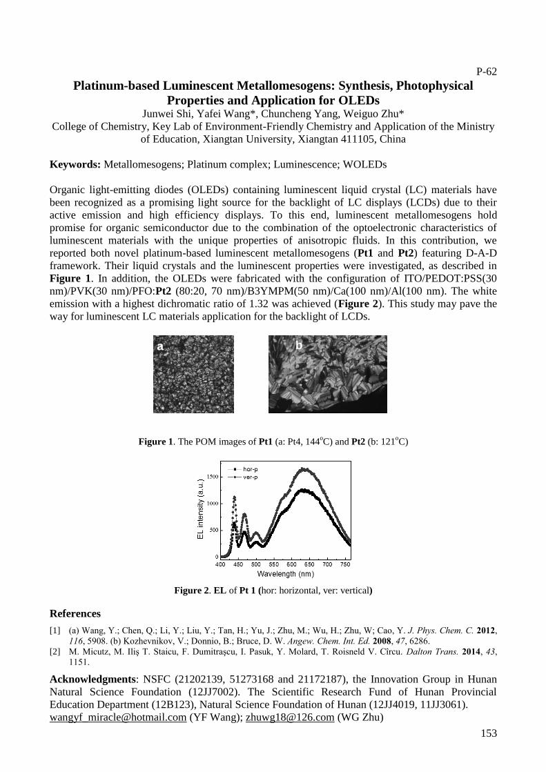
153
P-62
Platinum-based Luminescent Metallomesogens: Synthesis, Photophysical
Properties and Application for OLEDs Junwei Shi, Yafei Wang*, Chuncheng Yang, Weiguo Zhu*
College of Chemistry, Key Lab of Environment-Friendly Chemistry and Application of the Ministry
of Education, Xiangtan University, Xiangtan 411105, China
Keywords: Metallomesogens; Platinum complex; Luminescence; WOLEDs
Organic light-emitting diodes (OLEDs) containing luminescent liquid crystal (LC) materials have
been recognized as a promising light source for the backlight of LC displays (LCDs) due to their
active emission and high efficiency displays. To this end, luminescent metallomesogens hold
promise for organic semiconductor due to the combination of the optoelectronic characteristics of
luminescent materials with the unique properties of anisotropic fluids. In this contribution, we
reported both novel platinum-based luminescent metallomesogens (Pt1 and Pt2) featuring D-A-D
framework. Their liquid crystals and the luminescent properties were investigated, as described in
Figure 1. In addition, the OLEDs were fabricated with the configuration of ITO/PEDOT:PSS(30
nm)/PVK(30 nm)/PFO:Pt2 (80:20, 70 nm)/B3YMPM(50 nm)/Ca(100 nm)/Al(100 nm). The white
emission with a highest dichromatic ratio of 1.32 was achieved (Figure 2). This study may pave the
way for luminescent LC materials application for the backlight of LCDs.
Figure 1. The POM images of Pt1 (a: Pt4, 144oC) and Pt2 (b: 121
oC)
Figure 2. EL of Pt 1 (hor: horizontal, ver: vertical)
References
[1] (a) Wang, Y.; Chen, Q.; Li, Y.; Liu, Y.; Tan, H.; Yu, J.; Zhu, M.; Wu, H.; Zhu, W; Cao, Y. J. Phys. Chem. C. 2012,
116, 5908. (b) Kozhevnikov, V.; Donnio, B.; Bruce, D. W. Angew. Chem. Int. Ed. 2008, 47, 6286.
[2] M. Micutz, M. Iliş T. Staicu, F. Dumitraşcu, I. Pasuk, Y. Molard, T. Roisneld V. Cîrcu. Dalton Trans. 2014, 43,
1151.
Acknowledgments: NSFC (21202139, 51273168 and 21172187), the Innovation Group in Hunan
Natural Science Foundation (12JJ7002). The Scientific Research Fund of Hunan Provincial
Education Department (12B123), Natural Science Foundation of Hunan (12JJ4019, 11JJ3061).
[email protected] (YF Wang); [email protected] (WG Zhu)
a b

154
P-63
Thickness Dependent Air-Exposure Induced Phase Transition of CuPc Ultra-
Thin Films to Well-Ordered One-Dimensional Nanocrystals on Layered-
Substrates
Lei Zhang1,a)
, Yingguo Yang2, Han Huang
1,3,b), Lu Lyu
1, Hong Zhang
1, Ningtong Cao
1, Haipeng
Xie1, Xingyu Gao
2, Dongmei Niu
1,3, Yongli Gao
1,3,b)
1Institute of Super-microstructure and Ultrafast Process in Advanced Materials (ISUPAM), School of
Physics and Electronics, the Central South University, Changsha, Hunan 410083, P. R. China 2Shanghai Synchrotron Radiation Facility, Shanghai Institute of Applied Physics, Chinese Academy
of Sciences, 239 Zhangheng Road, Pudong New Area, Shanghai 201204, P. R. China 3Hunan Key Laboratory for Super-microstructure and Ultrafast Process , the Central South
University, Changsha, Hunan 410083, P. R. China
Keywords: CuPc, layered substrates, nanocrystals, air exposure, phase transition
Highly ordered organic crystals are important building blocks for future high-performance organic
nanodevices. Here we report a feasible way to produce arrays of well-ordered one-dimensional (1D)
CuPc nanocrystals by using MoS2 or HOPG as templates. The growth behaviors of CuPc on MoS2 as
well as on HOPG and corresponding effects of air-exposure were systematically investigated by
means of in situ photoemission spectroscopy (PES) and low-energy electron diffraction (LEED),
combined with ex situ atomic force microscope (AFM), grazing incidence X-ray diffraction
(GIXRD) and Raman. In situ PES and LEED results show that CuPc molecules adopt an face-on
configuration at the thickness up to 4.8nm, consistent with previous reports [1,2], while ex situ AFM
and GIXRD results show 1D nanocrystals with molecules in an edge-on configuration for 4.8 nm-
thick CuPc. Detailed analyses show that the formation of these 1D nanocrystals is closely related to
the air exposure, CuPc thicknesses and growth temperature. Such 1D CuPc nanocrystals can be
further optimized by changing growth conditions and may have great potential for use in high-
performance organic devices.
Fig. LEED patterns of (a) MoS2(0001) and (b) 4.8nm-thick CuPc on it. (c) AFM image of 4.8 nm-
thick CuPc and corresponding 2D-GIXRD. (d) Out-of-plane GIXRD spectra of 1.2 and 4.8 nm-thick
CuPc films around the α-phase (100) peak.
a) Presenting author’s Email: [email protected]
b) Corresponding author’s Email: [email protected]; [email protected]
References:
(1)K. Xiao, W. Deng, J. K. Keum, M. Yoon, et al. J. Am. Chem. Soc. 2013, 135, 3680−3687. (2)T. Fukuma, K. Kobayashi, H. Yamada, K. Matsushige. J. Appl. Phys. 2004, 95, 4742-4746.

155
P-64
Elimination of the herringbone reconstruction of Au(111) surface by self-
assemblied HBB
Zhiyu Tan1, 2, a)
, Zhenhong Zhou1, 2
, Guo Tian1, 2
, Yongli Gao1, 2
, Han Huang1, 2, 3, b)
1Institute of Super Microstructure and Ultrafast Process in Advanced Materials,
2Hunan Key Laboratory for Super-
microstructure and Ultrafast Process, School of Physics and Electronics, Central South University, Changsha, Hunan
410083, PR China. 3Institute for Materials Microstructure, Central South University, Lushan South Road No. 932, Changsha 410083, Hunan,
P. R. China.
Key Words: Au(111); dereconstruction; HBB; STM
Au(111) reconstructs at room temperature into the well-known (22×√3) superstructure due to a
unidirectional compression along the <110> directions of the top gold layer, leading to 23 top layer
gold atoms in 22 bulk lattice atomic spaces. Utilization and manipulation of these reconstructions are
active fields in surface science. The effect of the self-assembly monolayer HBB film on the Au(111)
surface reconstruction has been studied by high-resolved Scanning Tunneling Microscopy (STM).
Under UHV condition, the herringbone reconstruction pattern on clean Au(111) surface is clearly
observed. Upon deposition of sub-monolayer HBB molecules, part of herringbone reconstruction on
Au(111) surface disappear. Molecular-resolved STM observation indicates that, HBB molecules are
in a square arrangement in the islands without herringbone reconstruction but surrounded by closed
soliton. In contrast, HBB molecules are in a hexagonal arrangement in the islands with visible
herringbone reconstruction and the corresponding reconstructed patterns were consecutive cross the
border of the molecule layer. The sub molecularly resolved STM images show that in the former
case HBB molecules lift some Au atoms from their equilibrium positions resulting in surface atom
density reducing and thus relieve Au(111) surface reconstruction, indicating stronger interaction with
substrate, On the contrary, a strong interaction is observed among HBB molecules with hexagonal
lattice, which barely influence the substrate. Giving geometric analysis, we put forward two possible
arrangements of HBB molecules.
FIG. STM images showing the two arrangements of HBB molecules on Au (111). (a) The
tetragonal lattice. (b) The concurrence of the tetragonal lattice and the hexagonal lattice. (c) the
hexagonal lattice.
a) [email protected] b) [email protected]
References: [1] Whitesides G M, Grzybowski B. Self-ass Whitesides G M, Grzybowski B. Self-assembly at all scales.
Science 295(5564), 2418-2421(2002).
[2] Felix Hanke, Jonas BjÖrk. Structure and local reactivity of the Au(111) surface reconstruction. Phys. Rev.
B 87, 235422(2013).
(a) (b) (c)
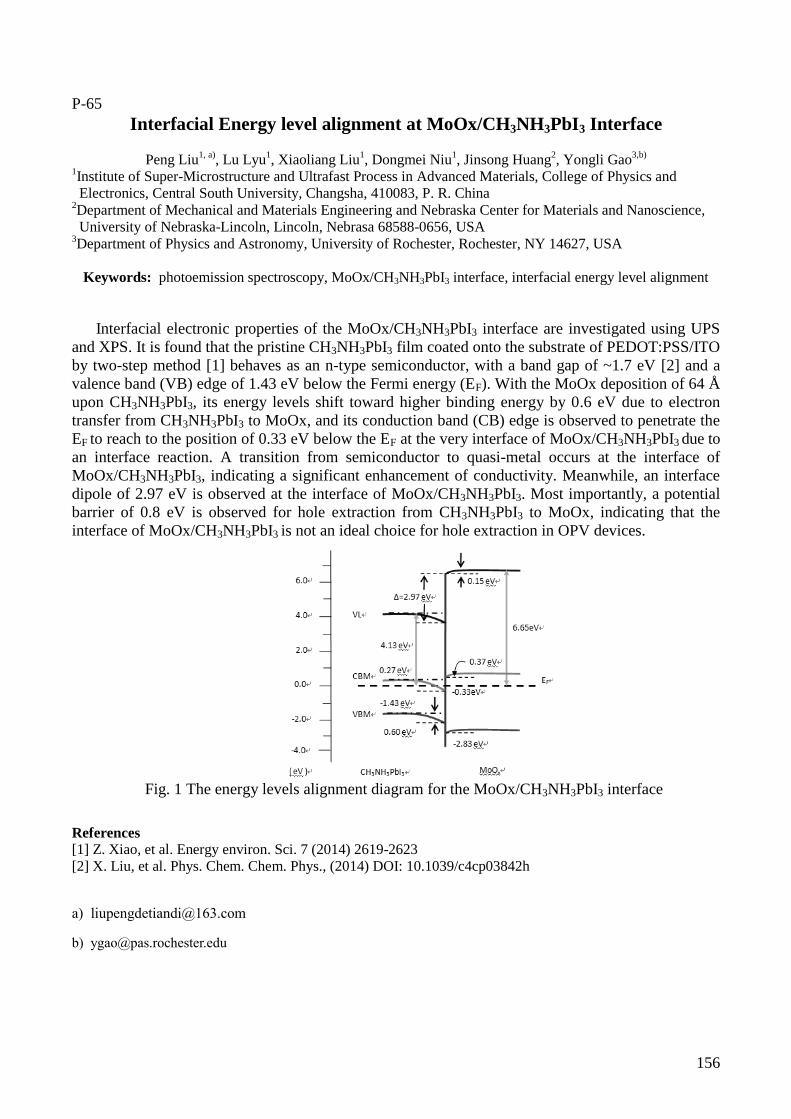
156
P-65
Interfacial Energy level alignment at MoOx/CH3NH3PbI3 Interface
Peng Liu1, a)
, Lu Lyu1, Xiaoliang Liu
1, Dongmei Niu
1, Jinsong Huang
2, Yongli Gao
3,b)
1Institute of Super-Microstructure and Ultrafast Process in Advanced Materials, College of Physics and
Electronics, Central South University, Changsha, 410083, P. R. China 2Department of Mechanical and Materials Engineering and Nebraska Center for Materials and Nanoscience,
University of Nebraska-Lincoln, Lincoln, Nebrasa 68588-0656, USA 3Department of Physics and Astronomy, University of Rochester, Rochester, NY 14627, USA
Keywords: photoemission spectroscopy, MoOx/CH3NH3PbI3 interface, interfacial energy level alignment
Interfacial electronic properties of the MoOx/CH3NH3PbI3 interface are investigated using UPS
and XPS. It is found that the pristine CH3NH3PbI3 film coated onto the substrate of PEDOT:PSS/ITO
by two-step method [1] behaves as an n-type semiconductor, with a band gap of ~1.7 eV [2] and a
valence band (VB) edge of 1.43 eV below the Fermi energy (EF). With the MoOx deposition of 64 Å
upon CH3NH3PbI3, its energy levels shift toward higher binding energy by 0.6 eV due to electron
transfer from CH3NH3PbI3 to MoOx, and its conduction band (CB) edge is observed to penetrate the
EF to reach to the position of 0.33 eV below the EF at the very interface of MoOx/CH3NH3PbI3 due to
an interface reaction. A transition from semiconductor to quasi-metal occurs at the interface of
MoOx/CH3NH3PbI3, indicating a significant enhancement of conductivity. Meanwhile, an interface
dipole of 2.97 eV is observed at the interface of MoOx/CH3NH3PbI3. Most importantly, a potential
barrier of 0.8 eV is observed for hole extraction from CH3NH3PbI3 to MoOx, indicating that the
interface of MoOx/CH3NH3PbI3 is not an ideal choice for hole extraction in OPV devices.
Fig. 1 The energy levels alignment diagram for the MoOx/CH3NH3PbI3 interface
References
[1] Z. Xiao, et al. Energy environ. Sci. 7 (2014) 2619-2623
[2] X. Liu, et al. Phys. Chem. Chem. Phys., (2014) DOI: 10.1039/c4cp03842h

157
P-66
Effects of precursor ratios on electronic structure and surface composition of
perovskite films
Haipeng Xie1,a)
, LuLyu1, Xiaoliang Liu
1, Dongmei Niu
1, Jinsong Huang
2, Yongli Gao
3, b)
1Hunan Key Laboratory for Super-microstructure and Ultrafast Process, School of Physics and Electronics,
Central South University, Changsha, Hunan 410083, China 2Department of Mechanical and Materials Engineering and Nebraska Center for Materials and Nanoscience,
University of Nebraska-Lincoln, Lincoln, Nebraska 68588-0656, USA 3Department of Physics and Astronomy, University of Rochester, Rochester, NY 14627, USA
Keywords: CH3NH3PbI3, UPS, XPS, precursor ratio, annealing
The characteristics of high absorption coefficient, appropriate direct bandgap, excellent carrier transport,
low cost, and solution-based fabrication process make the organometallic halide perovskites have attracted
intensive interest in recent years. [1-2] We have investigated the electronic structure of the CH3NH3PbI3 films
fabricated by one-step method with different precursor ratios (PbI2/CH3NH3I) using ultraviolet photoemission
spectroscopy (UPS) and X-ray photoemission spectroscopy (XPS). It is found that the n to p type transition
can be adjusted by changing precursor ratios, [3] as shown in Fig. 1. The perovskite film shows heavily n-
doped behavior with the precursor ratio of 1.7, and the Fermi level is pushed down closer to valance band top
as reducing the precursor ratio, then the film is observed to be weak p-type with the precursor ratio of 0.3. The
XPS results show that the lead content for the perovskite film with 0.3 precursor ratio reaches the minimum,
indicating the existence of Pb vacancies to lead to the formation of p-type film. Furthermore, we have
investigated the effects of annealing on the electronic structure and surface composition of perovskite films.
We find that the perovskite film with 0.3 precursor ratio can be changed from p-type to n-type after annealing
due to the reduction of iodine content.
Fig. 1 The energy levels of perovskite films with different precursor
ratios. (a) 1.7 precursor ratio, (b) 1.0 precursor ratio, (c) 0.65 precursor
ratio, (d) 0.3 precursor ratio, (e) 0.3 precursor ratio film after
annealing.
References [1] A. Kojima, K. Teshima, et al., J. Am. Chem. Soc., 131 (2009)
6050-6051
[2] H.P. Zhou, Q. Chen, et al., Science, 345 (2014) 542-546.
[3] Q. Wang, Y.C. Shao, et al. Appl. Phys. Lett., 105 (2014) 163508
a) E-mail: [email protected]
b) E-mail: [email protected]
158
P-67
The Study of Spectroscopic Properties of Colloidal Solutions of
Superparamagnetic Nanoparticles (Fe3O4/SiO2)
R.S. Smerdov1,a)
, T.V. Bocharova1,b)
1Saint-Petersburg State Polytechnycal University, Saint-Petersburg, Russia
Keywords: Magnetite Nanoparticles, Fe3O4/SiO2 Composite Nanoparticles, UV-Vis spectroscopy,
Biomolecular Electronics, G. Mie Theory.
The development of novel methods of medical diagnostics such as magnetic resonance imaging
(MRI), positron emission tomography, X-ray computed tomography has required further research in the
field of agents for contrast-enhanced imaging [1]. Composite superparamagnetic Fe3O4 nanoparticles
could be considered as negative contrast agents reducing spin-spin relaxation time. Furthermore, due to
their biocompatibility magnetic nanoparticles may be also used as magnetic drug-targeting agents [2] and
as a potential medium for magnetic hyperthermia in high-frequency AC magnetic field [3]. Optical
properties of thin magnetite films are of great interest: such films demonstrate UV absorption and decent
transmission in visible region allowing to consider nano-sized magnetite as a promising optoelectronic
material [4].
The research presented in this thesis has two distinct objectives. The first objective is identification
of parameters of the optical absorption spectra of colloidal solutions of magnetic nanoparticles. The
second objective is to create a structure model of a single composite Fe3O4/SiO2 nanoparticle. Specord®
40 Analytik Jena was used to fulfill measurements of optical absorption spectra of the samples at the
temperature of 300K.
According to P. Levy [5], the shape of the absorption bands is considered to be Gaussian [Eq. (1);
where К0 corresponds to absorbance at the wavelength of an absorption band maximum, U is the half-
width of an absorption band (cm-1) and ν0 is the position of an absorption band maximum (cm-1)] .
2
020
2ln4exp)(
UKK (1)
The appearance of absorption spectra of colloidal solutions indicates the identity of the chemical
composition. Alternation in the concentration of Fe3O4 nanoparticles deposited on the SiO2 gel matrix
during the Massart reaction was obvious and the largest concentration of Fe3O4 nanoparticles is detected
while using a solution of tetraethoxysylane (TEOS) in isopropanol with the concentration of TEOS 60
vol. %.
As a result of mathematical treatment of absorption spectra using Origin© 8.1 six distinctive
absorption bands in UV region corresponding to the following maxima were discovered: 25130 cm-1, 26220 cm-
1, 27300 cm-1, 28480 cm-1, 29530 cm-1 and 30480 cm-1 with intrinsic half-width remaining constant. The
presence of these bands is suggested to be due to the formation of Fe3O4 clusters on the surface of the gel
matrix with six characteristic dimensions. Absorption maxima observed at a concentration of TEOS 60 vol.
% and associated with clusters of all sizes are caused by the interaction of clusters. Cluster size was estimated
using G. Mie Theory [6]. References
1. NaH Bin, et al. Adv. Mater. 21, 2133–2148 (2009).
2. Liao Z, Wang H, Lv R, et al. Polymeric liposomes-coated superparamagnetic iron oxide nanoparticles as contrast
agent for targeted magnetic resonance imaging of cancer cells. Langmuir 2011;27:3100-5.
3.Kappiyoor R et al. The effects of magnetic nanoparticle properties on magnetic fluid hyperthermia. J Appl . Phys.
2010;108:094702.
4. Chang-Neng, et al. Magnetic and Optical Properties of Isolated Magnetite Nanocrystals. Materials Transactions, Vol.
48, No. 5 (2007) pp. 1143 to 1148.
5. Levy P.W. The kinetics of gamma-ray induced coloring of glass.//J. American Cerafic Society.- 1960 – V.4, N 8, – P.
389-395.
6. Kreibig U, Small Silver Particles in Photosensitive Glass: Their Nucleation and Growth, Appl. Phys. 1976. V. 10. P.
255-264.
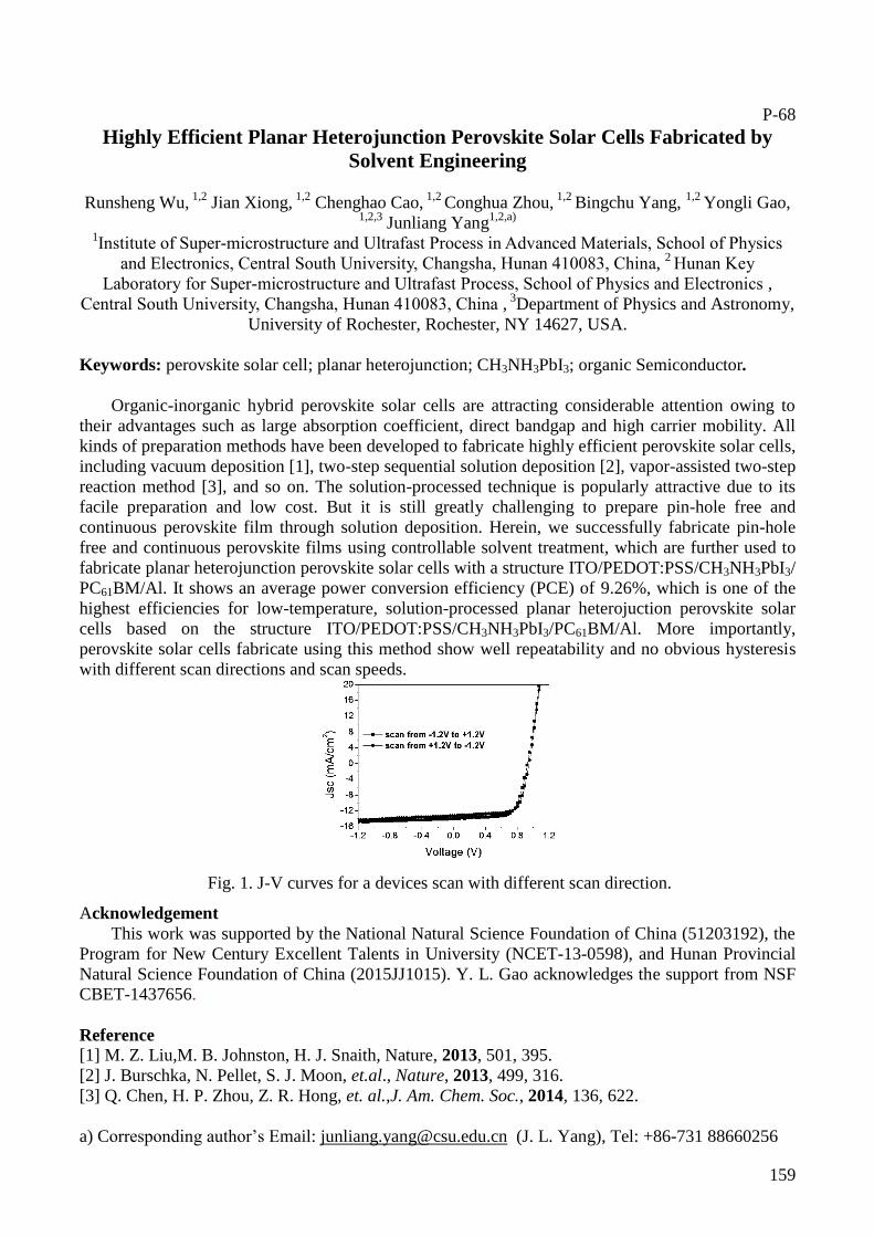
159
P-68
Highly Efficient Planar Heterojunction Perovskite Solar Cells Fabricated by
Solvent Engineering
Runsheng Wu, 1,2
Jian Xiong, 1,2
Chenghao Cao, 1,2
Conghua Zhou, 1,2
Bingchu Yang, 1,2
Yongli Gao,
1,2,3 Junliang Yang
1,2,a)
1Institute of Super-microstructure and Ultrafast Process in Advanced Materials, School of Physics
and Electronics, Central South University, Changsha, Hunan 410083, China, 2 Hunan Key
Laboratory for Super-microstructure and Ultrafast Process, School of Physics and Electronics ,
Central South University, Changsha, Hunan 410083, China , 3
Department of Physics and Astronomy,
University of Rochester, Rochester, NY 14627, USA.
Keywords: perovskite solar cell; planar heterojunction; CH3NH3PbI3; organic Semiconductor.
Organic-inorganic hybrid perovskite solar cells are attracting considerable attention owing to
their advantages such as large absorption coefficient, direct bandgap and high carrier mobility. All
kinds of preparation methods have been developed to fabricate highly efficient perovskite solar cells,
including vacuum deposition [1], two-step sequential solution deposition [2], vapor-assisted two-step
reaction method [3], and so on. The solution-processed technique is popularly attractive due to its
facile preparation and low cost. But it is still greatly challenging to prepare pin-hole free and
continuous perovskite film through solution deposition. Herein, we successfully fabricate pin-hole
free and continuous perovskite films using controllable solvent treatment, which are further used to
fabricate planar heterojunction perovskite solar cells with a structure ITO/PEDOT:PSS/CH3NH3PbI3/
PC61BM/Al. It shows an average power conversion efficiency (PCE) of 9.26%, which is one of the
highest efficiencies for low-temperature, solution-processed planar heterojuction perovskite solar
cells based on the structure ITO/PEDOT:PSS/CH3NH3PbI3/PC61BM/Al. More importantly,
perovskite solar cells fabricate using this method show well repeatability and no obvious hysteresis
with different scan directions and scan speeds.
Fig. 1. J-V curves for a devices scan with different scan direction.
Acknowledgement
This work was supported by the National Natural Science Foundation of China (51203192), the
Program for New Century Excellent Talents in University (NCET-13-0598), and Hunan Provincial
Natural Science Foundation of China (2015JJ1015). Y. L. Gao acknowledges the support from NSF
CBET-1437656.
Reference
[1] M. Z. Liu,M. B. Johnston, H. J. Snaith, Nature, 2013, 501, 395.
[2] J. Burschka, N. Pellet, S. J. Moon, et.al., Nature, 2013, 499, 316.
[3] Q. Chen, H. P. Zhou, Z. R. Hong, et. al.,J. Am. Chem. Soc., 2014, 136, 622.
a) Corresponding author’s Email: [email protected] (J. L. Yang), Tel: +86-731 88660256
160
P-69
Boosting the Power Conversion Efficiency of Organic Solar Cells Using Weakly
Luminescent Gold(III) Corrole with Long-Lived Exciton State
Shiu-Lun Laia)
, Lin Wang, Chen Yang, Mei-Yee Chan, Xiangguo Guan, Chi-Chung Kwok, Chi-
Ming Cheb)
State Key Laboratory of Synthetic Chemistry, HKU-CAS Joint Laboratory on New Materials and Department of
Chemistry, The University of Hong Kong, Pokfulam Road, Hong Kong
Keywords: organic solar cell, photo-conversion, triplet state, gold-corrole, and electron-donor.
Transition metal complexes have been widely used as light-emitting and photon-absorbing materials
in optoelectronic devices with diverse applications. While these complexes have been intensively studied
in the field of organic light-emitting devices (OLEDs) due to their inherently high phosphorescence
quantum yields (), they are rarely employed in the fabrication of organic solar cells (OSCs) with
reported examples showing poor photovoltaic responses with unexpectedly low power conversion
efficiency (PCE) of 2.9% for most of the vacuum-deposited devices or 5.0% for solution-processed
devices in the literature. Here, we successfully employed weakly luminescent gold(III) corrole, namely
HKU-AuC, as photon-absorber which can effectively boost up the PCE of OSCs to 6% under 1 sun
AM1.5G simulated light illumination with high short-circuit current density of 14.2 mA cm–2 and fill
factor of 0.57, which is the highest value among the reported PCE for OSCs incorporating metal-organic
complexes. The superior device performance may be ascribed to the weakly emissive nature with low
of 0.04% and long excited state lifetime of 63 s of HKU-AuC, which can minimize recombination loss
and favor exciton-dissociation. A broad absorption covering the entire visible spectral region has also
been observed, which is originated from mixing excited states of triplet ligand-to-metal charge-transfer
and singlet ligand-centered * transitions. These distinct features of HKU-AuC may account for the
significant increase in the photocurrent and PCE of OSCs. More importantly, the is suggested to play
an important role affecting the PCE and can be used to rationalize the inferior OSC performance based on
other phosphorescent organometallic complexes. This work demonstrates for the first time to employ
gold(III) complex as donor and opens up a new avenue to fully utilize transition metals for the
fabrication of OSCs.
This work was supported by the Theme-Based Research Scheme (T23-713/11), the Innovation and
Technology Commission of the HKSAR Government (ITS/310/11), and the National Key Basic
Research Program of China (No. 2013CB834802).
FIG 1. Mechanisms of the photoconversion in OSCs with triplet photoactive materials. ηTOTAL, ηA, ηED, and ηCC
are the total, light-absorption, exciton-dissociation and charge-collection efficiencies, respectively.
RELEVANT PUBLICATION
S.-L. Lai, L. Wang, C. Yang, M.-Y. Chan, X. Guan, C.-C. Kwok, and C.-M. Che, Adv. Funct. Mater. 2014, 24,
4655–4665. (Highlighted as the FRONTISPIECE)
a) Presenting author’s email: [email protected] b) Corresponding author’s email: [email protected]

161
List of Participants
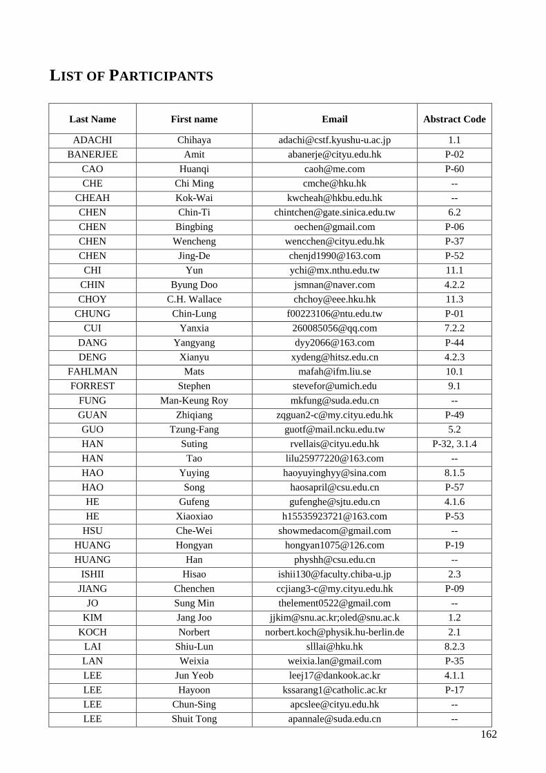
162
LIST OF PARTICIPANTS
Last Name First name Email Abstract Code
ADACHI Chihaya [email protected] 1.1
BANERJEE Amit [email protected] P-02
CAO Huanqi [email protected] P-60
CHE Chi Ming [email protected] --
CHEAH Kok-Wai [email protected] --
CHEN Chin-Ti [email protected] 6.2
CHEN Bingbing [email protected] P-06
CHEN Wencheng [email protected] P-37
CHEN Jing-De [email protected] P-52
CHI Yun [email protected] 11.1
CHIN Byung Doo [email protected] 4.2.2
CHOY C.H. Wallace [email protected] 11.3
CHUNG Chin-Lung [email protected] P-01
CUI Yanxia [email protected] 7.2.2
DANG Yangyang [email protected] P-44
DENG Xianyu [email protected] 4.2.3
FAHLMAN Mats [email protected] 10.1
FORREST Stephen [email protected] 9.1
FUNG Man-Keung Roy [email protected] --
GUAN Zhiqiang [email protected] P-49
GUO Tzung-Fang [email protected] 5.2
HAN Suting [email protected] P-32, 3.1.4
HAN Tao [email protected] --
HAO Yuying [email protected] 8.1.5
HAO Song [email protected] P-57
HE Gufeng [email protected] 4.1.6
HE Xiaoxiao [email protected] P-53
HSU Che-Wei [email protected] --
HUANG Hongyan [email protected] P-19
HUANG Han [email protected] --
ISHII Hisao [email protected] 2.3
JIANG Chenchen [email protected] P-09
JO Sung Min [email protected] --
KIM Jang Joo [email protected];[email protected] 1.2
KOCH Norbert [email protected] 2.1
LAI Shiu-Lun [email protected] 8.2.3
LAN Weixia [email protected] P-35
LEE Jun Yeob [email protected] 4.1.1
LEE Hayoon [email protected] P-17
LEE Chun-Sing [email protected] --
LEE Shuit Tong [email protected] --
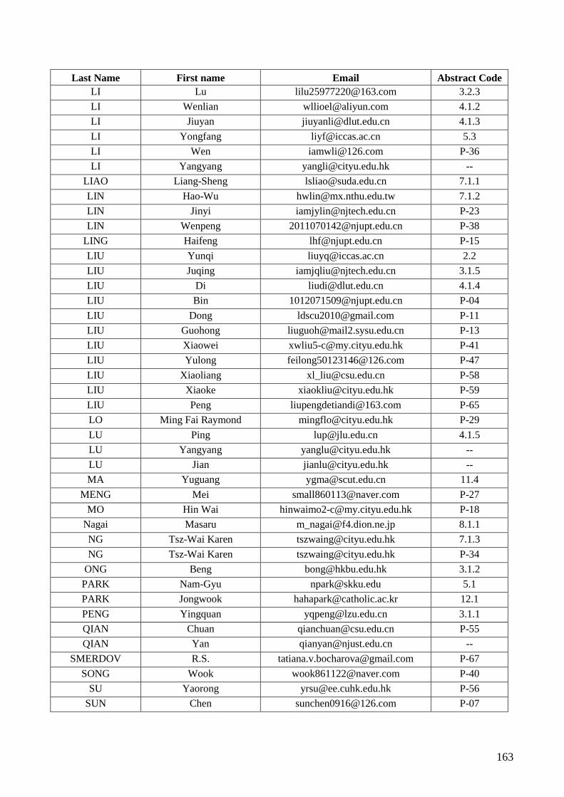
163
Last Name First name Email Abstract Code
LI Lu [email protected] 3.2.3
LI Wenlian [email protected] 4.1.2
LI Jiuyan [email protected] 4.1.3
LI Yongfang [email protected] 5.3
LI Wen [email protected] P-36
LI Yangyang [email protected] --
LIAO Liang-Sheng [email protected] 7.1.1
LIN Hao-Wu [email protected] 7.1.2
LIN Jinyi [email protected] P-23
LIN Wenpeng [email protected] P-38
LING Haifeng [email protected] P-15
LIU Yunqi [email protected] 2.2
LIU Juqing [email protected] 3.1.5
LIU Di [email protected] 4.1.4
LIU Bin [email protected] P-04
LIU Dong [email protected] P-11
LIU Guohong [email protected] P-13
LIU Xiaowei [email protected] P-41
LIU Yulong [email protected] P-47
LIU Xiaoliang [email protected] P-58
LIU Xiaoke [email protected] P-59
LIU Peng [email protected] P-65
LO Ming Fai Raymond [email protected] P-29
LU Ping [email protected] 4.1.5
LU Yangyang [email protected] --
LU Jian [email protected] --
MA Yuguang [email protected] 11.4
MENG Mei [email protected] P-27
MO Hin Wai [email protected] P-18
Nagai Masaru [email protected] 8.1.1
NG Tsz-Wai Karen [email protected] 7.1.3
NG Tsz-Wai Karen [email protected] P-34
ONG Beng [email protected] 3.1.2
PARK Nam-Gyu [email protected] 5.1
PARK Jongwook [email protected] 12.1
PENG Yingquan [email protected] 3.1.1
QIAN Chuan [email protected] P-55
QIAN Yan [email protected] --
SMERDOV R.S. [email protected] P-67
SONG Wook [email protected] P-40
SU Yaorong [email protected] P-56
SUN Chen [email protected] P-07
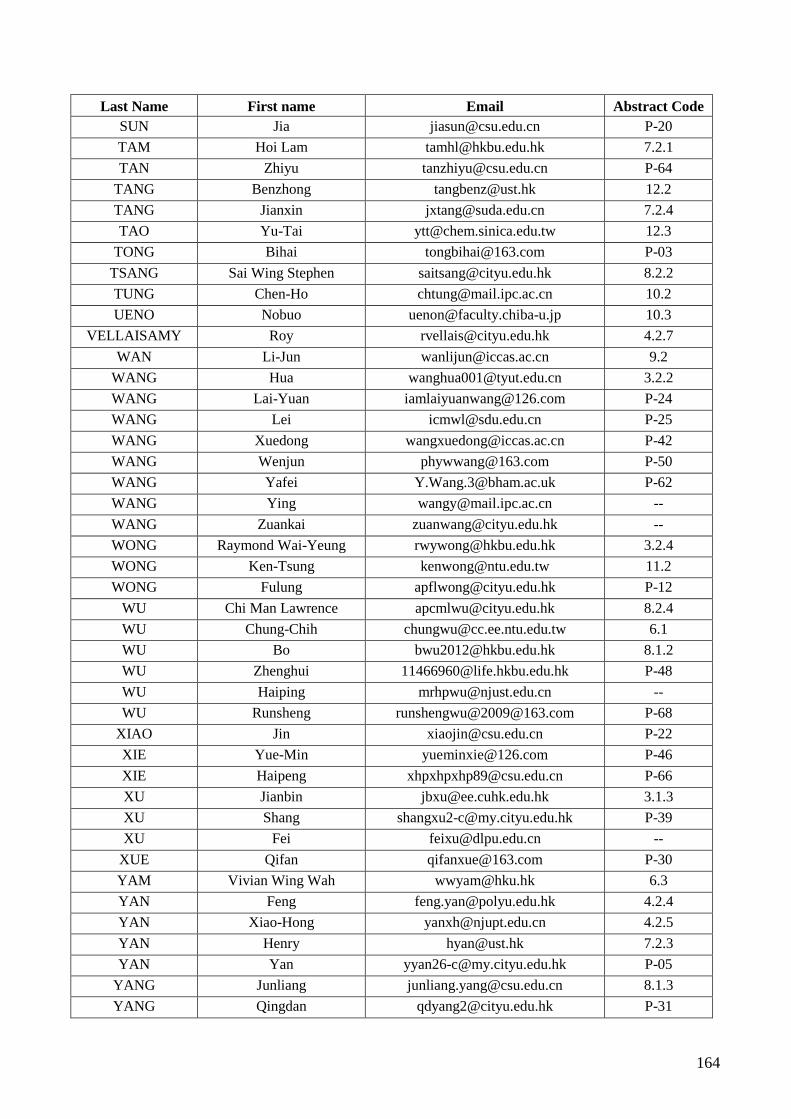
164
Last Name First name Email Abstract Code
SUN Jia [email protected] P-20
TAM Hoi Lam [email protected] 7.2.1
TAN Zhiyu [email protected] P-64
TANG Benzhong [email protected] 12.2
TANG Jianxin [email protected] 7.2.4
TAO Yu-Tai [email protected] 12.3
TONG Bihai [email protected] P-03
TSANG Sai Wing Stephen [email protected] 8.2.2
TUNG Chen-Ho [email protected] 10.2
UENO Nobuo [email protected] 10.3
VELLAISAMY Roy [email protected] 4.2.7
WAN Li-Jun [email protected] 9.2
WANG Hua [email protected] 3.2.2
WANG Lai-Yuan [email protected] P-24
WANG Lei [email protected] P-25
WANG Xuedong [email protected] P-42
WANG Wenjun [email protected] P-50
WANG Yafei [email protected] P-62
WANG Ying [email protected] --
WANG Zuankai [email protected] --
WONG Raymond Wai-Yeung [email protected] 3.2.4
WONG Ken-Tsung [email protected] 11.2
WONG Fulung [email protected] P-12
WU Chi Man Lawrence [email protected] 8.2.4
WU Chung-Chih [email protected] 6.1
WU Bo [email protected] 8.1.2
WU Zhenghui [email protected] P-48
WU Haiping [email protected] --
WU Runsheng runshengwu@[email protected] P-68
XIAO Jin [email protected] P-22
XIE Yue-Min [email protected] P-46
XIE Haipeng [email protected] P-66
XU Jianbin [email protected] 3.1.3
XU Shang [email protected] P-39
XU Fei [email protected] --
XUE Qifan [email protected] P-30
YAM Vivian Wing Wah [email protected] 6.3
YAN Feng [email protected] 4.2.4
YAN Xiao-Hong [email protected] 4.2.5
YAN Henry [email protected] 7.2.3
YAN Yan [email protected] P-05
YANG Junliang [email protected] 8.1.3
YANG Qingdan [email protected] P-31

165
Last Name First name Email Abstract Code
YIP Hin-Lap Angus [email protected] 8.1.4
YU Haomiao [email protected] P-16
YU Denis [email protected] --
ZAPIEN Antonio [email protected] --
ZENG Hui [email protected] P-61
ZHAN Yawen [email protected] P-45
ZHANG Hong [email protected] 3.2.5
ZHANG Jian [email protected] 4.2.1
ZHANG Hong [email protected] 7.1.4
ZHANG Dan [email protected] P-10
ZHANG Jie [email protected] P-21
ZHANG Tianyou [email protected] P-33
ZHANG Lu [email protected] P-51
ZHANG Lei [email protected] P-54
ZHANG Lei [email protected] P-63
ZHANG Wenjun [email protected] --
ZHAO Chen [email protected] P-08
ZHENG Xujun [email protected] P-43
ZHOU Ye [email protected] P-14
ZHOU Lei [email protected] P-26
ZHU Furong [email protected] 8.2.1
ZHU Xu-Hui [email protected] 8.2.5
ZHU Mengjian [email protected] P-28
ZOU Dechun [email protected] 3.2.1