Embed Size (px)
Citation preview

PCMFxUSB3B/C seriesCommon-mode EMI filter for differential channels withintegrated bidirectional ESD protectionRev. 2 — 29 January 2019 Product data sheet
1. General descriptionCommon-mode ElectroMagnetic Interference (EMI) filters with integrated bidirectional ElectroStaticDischarge (ESD) protection for one, two and three differential channels. The devices are designedto provide low insertion loss for differential high-speed signals on each channel while unwantedcommon-mode signals are attenuated.
Each differential channel incorporates two signal lines that are coupled by integrated coils. Diodesprovide protection to downstream components from ESD voltages up to ±20 kV on each signal line.
Table 1. Product overviewType number Number of channels Package NamePCMF1USB3B/C 1 WLCSP5
PCMF2USB3B/C 2 WLCSP10
PCMF3USB3B/C 3 WLCSP15
2. Features and benefits• One, two and three differential channels common-mode EMI filters with integrated ESD
protection• ESD protection up to ±20 kV contact discharge according to IEC 61000-4-2• Superior common-mode suppression over a wide frequency range• Superior RF performance compared to other integrated filters or discrete filters with external
ESD protection• Extremely high symmetry between line pairs• Industry-standard Wafer-Level Chip-Scale Packages: WLCSP5, 10 and 15 for smaller footprint
3. Applications• Smartphone, cellular and cordless phone• USB 3.2, USB 2.0, HDMI 2.0, HDMI 1.4• General-purpose downstream ESD protection for differential data lines• Tablet PC and Mobile Internet Device (MID)• MIPI M-PHY and D-PHY as used in Camera Serial Interface (CSI) and Display Serial Interface
(DSI)

Nexperia PCMFxUSB3B/C seriesCommon-mode EMI filter for differential channels with integrated bidirectional ESD protection
4. Pinning information
Table 2. PinningPin Symbol Description Simplified outline Graphic symbolPCMF1USB3B/C (WLCSP5_2-1-2)A1 CH1_IN+ channel 1+, external
A2 CH1_IN- channel 1-, external
B1 GND_CH1 ground channel 1
C1 CH1_OUT+ channel 1+, internal
C2 CH1_OUT- channel 1-, internalA B C
B1
1
2
Transparent top view
WLCSP5_2-1-2
A1
A2
C1
C2
aaa-028492B1
PCMF2USB3B/C (WLCSP10_4-2-4)A1 CH1_IN+ channel 1+, external
A2 CH1_IN- channel 1-, external
A3 CH2_IN+ channel 2+, external
A4 CH2_IN- channel 2-, external
B1 GND_CH1 ground channel 1
B2 GND_CH2 ground channel 2
C1 CH1_OUT+ channel 1+, internal
C2 CH1_OUT- channel 1-, internal
C3 CH2_OUT+ channel 2+, internal
C4 CH2_OUT- channel 2-, internal
A B C
B1
B2
1
2
3
4
Transparent top view
WLCSP10_4-2-4
aaa-028493
A1, 3
A2, 4
C1, 3
C2, 4
B1, B2 - no internal connection
PCMF3USB3B/C (WLCSP15_6-3-6)A1 CH1_IN+ channel 1+, external
A2 CH1_IN- channel 1-, external
A3 CH2_IN+ channel 2+, external
A4 CH2_IN- channel 2-, external
A5 CH3_IN+ channel 3+, external
A6 CH3_IN- channel 3-, external
B1 GND_CH1 ground channel 1
B2 GND_CH2 ground channel 2
B3 GND_CH3 ground channel 3
C1 CH1_OUT+ channel 1+, internal
C2 CH1_OUT- channel 1-, internal
C3 CH2_OUT+ channel 2+, internal
C4 CH2_OUT- channel 2-, internal
C5 CH3_OUT+ channel 3+, internal
C6 CH3_OUT- channel 3-, internal
B2
B3
B1
1
2
3
4
5
6
A B C
Transparent top view
WLCSP15_6-3-6
aaa-028494
B1, B2, B3 - no internal connection
A1, 3, 5
A2, 4, 6
C1, 3, 5
C2, 4, 6
PCMFxUSB3B/C_SER All information provided in this document is subject to legal disclaimers. © Nexperia B.V. 2019. All rights reserved
Product data sheet Rev. 2 — 29 January 2019 2 / 20

Nexperia PCMFxUSB3B/C seriesCommon-mode EMI filter for differential channels with integrated bidirectional ESD protection
5. Ordering information
Table 3. Ordering informationPackageType numberName Description
PCMF1USB3B/C WLCSP5 wafer level chip-size package; 5 bumps (2-1-2)
PCMF2USB3B/C WLCSP10 wafer level chip-size package; 10 bumps (4-2-4)
PCMF3USB3B/C WLCSP15 wafer level chip-size package; 15 bumps (6-3-6)
6. Marking
Table 4. Marking codesType number Marking codePCMF1USB3B/C PF1B
PCMF2USB3B/C PF2B
PCMF3USB3B/C PF3B
7. Limiting values
Table 5. Limiting valuesIn accordance with the Absolute Maximum Rating System (IEC 60134).
Symbol Parameter Conditions Min Max UnitVI input voltage -4 4 V
IEC 61000-4-2, level 4;allinput pins to ground
• contact discharge -20 20 kV
• air discharge -20 20 kV
IEC 61000-4-2, level 4;alloutput pins to ground
• contact discharge -2 2 kV
VESD electrostatic dischargevoltage
• air discharge -2 2 kV
IPPM rated peak-pulsecurrent
tp = 8/20 μs -9.5 9.5 A
Tstg storage temperature -40 +125 °C
Tamb ambient temperature -40 +125 °C
PCMFxUSB3B/C_SER All information provided in this document is subject to legal disclaimers. © Nexperia B.V. 2019. All rights reserved
Product data sheet Rev. 2 — 29 January 2019 3 / 20

Nexperia PCMFxUSB3B/C seriesCommon-mode EMI filter for differential channels with integrated bidirectional ESD protection
8. Characteristics
8.1. Channel characteristics
Table 6. Channel characteristicsTamb = 25 °C unless otherwise specified.
Symbol parameter Conditions Min Typ Max UnitRS(ch) channel
seriesresistance
single line; inputto output
- - 2.6 - Ω
Cd diodecapacitance
f = 1 MHz; VI =2.5 V
[1] - 0.3 - pF
IRM reverseleakagecurrent
per line;VI = 4 V
- 1 100 nA
VBR breakdownvoltage
IR = 1 mA 6 9 - V
TLP; positivetransient
[2] - 0.22 - ΩRdyn dynamicresistance
TLP; negativetransient
[2] - 0.22 - Ω
[1] This parameter is guaranteed by design[2] 100 ns Transmission Line Pulse (TLP); 50 Ω; pulser at 70 ns to 90 ns.
8.2. Frequency characteristics
Table 7. Frequency characteristicsTamb = 25 °C unless otherwise specified.
Symbol Parameter Conditions Min Typ Max UnitDifferential mode: Sdd21
f-3dB cut-off frequency [1] - 8.1 - GHz
[1] Normalized to attenuation at 1 MHz.
PCMFxUSB3B/C_SER All information provided in this document is subject to legal disclaimers. © Nexperia B.V. 2019. All rights reserved
Product data sheet Rev. 2 — 29 January 2019 4 / 20

Nexperia PCMFxUSB3B/C seriesCommon-mode EMI filter for differential channels with integrated bidirectional ESD protection
aaa-028346
-3
-2
-4
-1
0
Sdd21(dB)
-5
f (Hz)107 10111010108 109
Fig. 1. Differential mode insertion loss; typical values
f (Hz)108 1010109
aaa-028347
-20
-30
-10
0
Scc21(dB)
-40
Fig. 2. Common-mode insertion loss; typical values
f (Hz)108 1010109
aaa-028363
-20
-30
-10
0
Sdd21(dB)
-40
CH1 to CH2
Fig. 3. Differential crosstalk; typical values
t (ns)43.9 44.744.544.1 44.3
aaa-028348
95
105
115
Zdif(Ω)
85
Z reference
Z DUT
tr = 200 ps
Fig. 4. Differential Time Domain Reflectometer (TDR)plot; typical values
PCMFxUSB3B/C_SER All information provided in this document is subject to legal disclaimers. © Nexperia B.V. 2019. All rights reserved
Product data sheet Rev. 2 — 29 January 2019 5 / 20

Nexperia PCMFxUSB3B/C seriesCommon-mode EMI filter for differential channels with integrated bidirectional ESD protection
Fig. 5. USB 3.2 eye diagram 10 Gbps, test board with PCMFxUSB3B/C; typical values
Fig. 6. USB 3.2 eye diagram 10 Gbps, test board without device; typical values
PCMFxUSB3B/C_SER All information provided in this document is subject to legal disclaimers. © Nexperia B.V. 2019. All rights reserved
Product data sheet Rev. 2 — 29 January 2019 6 / 20

Nexperia PCMFxUSB3B/C seriesCommon-mode EMI filter for differential channels with integrated bidirectional ESD protection
Fig. 7. USB 3.2 eye diagram 5 Gbps, test board with PCMFxUSB3B/C; typical values
Fig. 8. USB 3.2 eye diagram 5 Gbps, test board without device; typical values
PCMFxUSB3B/C_SER All information provided in this document is subject to legal disclaimers. © Nexperia B.V. 2019. All rights reserved
Product data sheet Rev. 2 — 29 January 2019 7 / 20

Nexperia PCMFxUSB3B/C seriesCommon-mode EMI filter for differential channels with integrated bidirectional ESD protection
1080p, 6 Gbps
Fig. 9. HDMI 2.0 eye diagram TP1, test board with PCMFxUSB3B/C; typical values
1080p, 6 Gbps
Fig. 10. HDMI 2.0 eye diagram TP1, test board without device; typical values
PCMFxUSB3B/C_SER All information provided in this document is subject to legal disclaimers. © Nexperia B.V. 2019. All rights reserved
Product data sheet Rev. 2 — 29 January 2019 8 / 20

Nexperia PCMFxUSB3B/C seriesCommon-mode EMI filter for differential channels with integrated bidirectional ESD protection
1080p, 6 Gbps
Fig. 11. HDMI 2.0 eye diagram TP2, test board with PCMFxUSB3B/C; typical values
1080p, 6 Gbps
Fig. 12. HDMI 2.0 eye diagram TP2, test board without device; typical values
PCMFxUSB3B/C_SER All information provided in this document is subject to legal disclaimers. © Nexperia B.V. 2019. All rights reserved
Product data sheet Rev. 2 — 29 January 2019 9 / 20

Nexperia PCMFxUSB3B/C seriesCommon-mode EMI filter for differential channels with integrated bidirectional ESD protection
VCL (V)0 252010 155
aaa-028357
10
15
5
20
25
I(A)
0
Transmission Line Pulse (TLP) = 100 ns;measured CH_IN to GND
Fig. 13. Dynamic resistance with positive clamping;typical values
VCL (V)-25 0-5-15 -10-20
aaa-028358
-15
-10
-20
-5
0
I(A)
-25
Transmission Line Pulse (TLP) = 100 ns;measured CH_IN to GND
Fig. 14. Dynamic resistance with negative clamping;typical values
VCL (V)0 806020 40
aaa-028359
40
20
60
80
I(A)
0
Very-Fast Transmission Line Pulse(VF-TLP) = 5 ns;measured CH_IN to GND
Fig. 15. Dynamic resistance with positive clamping;typical values
VCL (V)-80 0-20-60 -40
aaa-028360
-40
-60
-20
0
I(A)
-80
Very-Fast Transmission Line Pulse(VF-TLP) = 5 ns;measured CH_IN to GND
Fig. 16. Dynamic resistance with negative clamping;typical values
The device uses an advanced clamping structure showing a negative dynamic resistance.This snap-back behavior strongly reduces the clamping voltage to the system behind the ESDprotection during an ESD event. Do not connect unlimited DC current sources to the data lines toavoid keeping the ESD protection device in snap-back state after exceeding breakdown voltage(due to an ESD pulse for instance).
PCMFxUSB3B/C_SER All information provided in this document is subject to legal disclaimers. © Nexperia B.V. 2019. All rights reserved
Product data sheet Rev. 2 — 29 January 2019 10 / 20

Nexperia PCMFxUSB3B/C seriesCommon-mode EMI filter for differential channels with integrated bidirectional ESD protection
VCL (V)0 1084 62
aaa-028361
4
6
2
8
10
I(A)
0
IEC61000-4-5; tp = 8/20 μs; positive pulse
Fig. 17. Dynamic resistance with positive clamping;typical values
VCL (V)-10 0-2-6 -4-8
aaa-028362
-6
-4
-8
-2
0
I(A)
-10
IEC61000-4-5; tp = 8/20 μs; negative pulse
Fig. 18. Dynamic resistance with negative clamping;typical values
PCMFxUSB3B/C_SER All information provided in this document is subject to legal disclaimers. © Nexperia B.V. 2019. All rights reserved
Product data sheet Rev. 2 — 29 January 2019 11 / 20

Nexperia PCMFxUSB3B/C seriesCommon-mode EMI filter for differential channels with integrated bidirectional ESD protection
9. Application informationThe device is designed to provide high-level ESD protection for differential high-speed data linepairs such as:
• USB 3.2• HDMI 2.0• Transition-Minimized Differential Signaling (TMDS)• DisplayPort• external Serial Advanced Technology Attachment (eSATA)• Low Voltage Differential Signaling (LVDS)
When designing the Printed-Circuit Board (PCB), give careful consideration to impedance matchingand signal coupling. Do not connect the protected signal lines to unlimited current sources like, forexample, a battery.
Fig. 19. Application diagram: protecting the differential data lines of a USB Type-Cconnector evaluation dongle with PCMF1USB3B/C
Since the SuperSpeed TX/RX lines are separated by GND or VBUS from the Hi-Speed lines,PCMF1USB3B/C makes it easy to achieve same signal lengths, straight routing, and optimalpositioning for ESD protection directly at the connector.
PCMFxUSB3B/C_SER All information provided in this document is subject to legal disclaimers. © Nexperia B.V. 2019. All rights reserved
Product data sheet Rev. 2 — 29 January 2019 12 / 20

Nexperia PCMFxUSB3B/C seriesCommon-mode EMI filter for differential channels with integrated bidirectional ESD protection
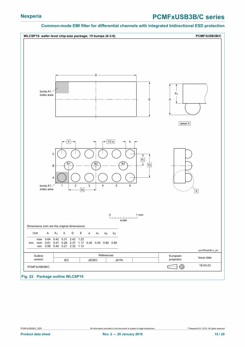
10. Package outline
ReferencesOutlineversion
Europeanprojection Issue date
IEC JEDEC JEITA
PCMF1USB3B/C
pcmf1usb3b-c_po
Unit
mmmaxnommin
0.64 0.42 0.82 1.22
A
Dimensions (mm are the original dimensions)
WLCSP5: wafer level chip-size package; 5 bumps (2-1-2) PCMF1USB3B/C
A1 b
0.31
D E e e1 e2
0.800.61 0.41 0.77 1.17 0.40 0.400.260.58 0.40 0.72 1.120.21
0 1 mm
scale
detail X
A
A1
X
A
B
C
E
D
21
e2
e1
e
b
1/2 e
B1
bump A1index area
bump A1index area
18-03-23
Fig. 20. Package outline WLCSP5
PCMFxUSB3B/C_SER All information provided in this document is subject to legal disclaimers. © Nexperia B.V. 2019. All rights reserved
Product data sheet Rev. 2 — 29 January 2019 13 / 20

Nexperia PCMFxUSB3B/C seriesCommon-mode EMI filter for differential channels with integrated bidirectional ESD protection
ReferencesOutlineversion
Europeanprojection Issue date
IEC JEDEC JEITA
PCMF2USB3B/C
pcmf2usb3b-c_po
Unit
mmmaxnommin
0.64 0.42 1.62
1.52
1.22
A
Dimensions (mm are the original dimensions)
WLCSP10: wafer level chip-size package; 10 bumps (4-2-4) PCMF2USB3B/C
A1 b
0.31
D E e e1 e2
0.800.61 0.41 1.57 1.17 0.40 0.40
e3
0.800.260.58 0.40 1.120.21
0 1 mm
scale
detail X
A
A1
X
A
B
C
E
D
e2
e1B2B1
bump A1index area
bump A1index area
e b
43e3
21
1/2 e
18-03-23
Fig. 21. Package outline WLCSP10
PCMFxUSB3B/C_SER All information provided in this document is subject to legal disclaimers. © Nexperia B.V. 2019. All rights reserved
Product data sheet Rev. 2 — 29 January 2019 14 / 20
Nexperia PCMFxUSB3B/C seriesCommon-mode EMI filter for differential channels with integrated bidirectional ESD protection
ReferencesOutlineversion
Europeanprojection Issue date
IEC JEDEC JEITA
PCMF3USB3B/C
pcmf3usb3b-c_po
Unit
mmmaxnommin
0.64 0.42 2.42 1.220.80
A
Dimensions (mm are the original dimensions)
WLCSP15: wafer level chip-size package; 15 bumps (6-3-6) PCMF3USB3B/C
A1 b
0.31
D E e e1 e2
0.80
e3
0.61 0.41 2.37 1.17 0.40 0.400.260.58 0.40 2.32 1.120.21
0 1 mm
scale
detail X
A
A1
D
E
bump A1index area
bump A1index area X
e2
e
e1
e3
b
1 2 43 65
A
B
C
1/2 e
B1 B2 B3
18-03-23
Fig. 22. Package outline WLCSP15
PCMFxUSB3B/C_SER All information provided in this document is subject to legal disclaimers. © Nexperia B.V. 2019. All rights reserved
Product data sheet Rev. 2 — 29 January 2019 15 / 20

Nexperia PCMFxUSB3B/C seriesCommon-mode EMI filter for differential channels with integrated bidirectional ESD protection
11. Soldering
WLCSP5: Solder footprint and stencil aperture PCMF1USB3B/C
pcmf1usb3b-c_fr
solder resist opening (SR)
occupied area
solder land plus solder paste
solder paste deposit (SP)
solder land (SL)
Dimensions in mm
SRP
0.25 0.325
Hx
1.00
SL
0.25
SP
0.40
Hy
1.40
SL = SP
SR
detail X
seedetail X
P
P
Hx
Hy
recommend stencil thickness: 0.1 mm
18-03-23
Fig. 23. Soldering footprint WLCSP5 (PCMF1USB3B/C)
WLCSP10: Solder footprint and stencil aperture PCMF2USB3B/C
pcmf2usb3b-c_fr
solder resist opening (SR)
occupied area
solder land plus solder paste
solder paste deposit (SP)
solder land (SL)
Dimensions in mm
P1 SRP
0.80 0.25 0.325
Hx
1.80
SL
0.25
SP
0.40 18-03-23
Hy
1.40
SL = SP
SR
detail X
seedetail X
P
P
P1
Hx
Hy
recommend stencil thickness: 0.1 mm
Fig. 24. Soldering footprint WLCSP10 (PCMF2USB3B/C)
PCMFxUSB3B/C_SER All information provided in this document is subject to legal disclaimers. © Nexperia B.V. 2019. All rights reserved
Product data sheet Rev. 2 — 29 January 2019 16 / 20

Nexperia PCMFxUSB3B/C seriesCommon-mode EMI filter for differential channels with integrated bidirectional ESD protection
WLCSP15: Solder footprint and stencil aperture PCMF3USB3B/C
pcmf3usb3b-c_fr
solder resist opening (SR)
occupied area
solder land plus solder paste
solder paste deposit (SP)
solder land (SL)
Dimensions in mm
P1 SRP
0.80 0.25 0.325
Hx
2.60
SL
0.25
SP
0.40 18-03-23
recommend stencil thickness: 0.1 mmHy
1.40
SL = SP
SR
detail X
seedetail X
P
P
P1
Hx
Hy
Fig. 25. Soldering footprint WLCSP15 (PCMF3USB3B/C)
PCMFxUSB3B/C_SER All information provided in this document is subject to legal disclaimers. © Nexperia B.V. 2019. All rights reserved
Product data sheet Rev. 2 — 29 January 2019 17 / 20

Nexperia PCMFxUSB3B/C seriesCommon-mode EMI filter for differential channels with integrated bidirectional ESD protection
12. Revision history
Table 8. Revision historyDocument ID Release
dateData sheet status Change
noticeSupersedes
PCMFxUSB3B_C_SER v.2 20190129 Product data sheet - PCMFxUSB3B_C_SER v.1
Modifications: • Limiting values: Tamb updated.• Channel characteristics: Sentence inserted; RS(ch) inserted.• Frequency characteristics: Sentence inserted; Fig 2 updated.
PCMFxUSB3B_C_SER v.1 20180507 Product data sheet - -
PCMFxUSB3B/C_SER All information provided in this document is subject to legal disclaimers. © Nexperia B.V. 2019. All rights reserved
Product data sheet Rev. 2 — 29 January 2019 18 / 20

Nexperia PCMFxUSB3B/C seriesCommon-mode EMI filter for differential channels with integrated bidirectional ESD protection
13. Legal information
Data sheet status
Document status[1][2]
Productstatus [3]
Definition
Objective [short]data sheet
Development This document contains data fromthe objective specification forproduct development.
Preliminary [short]data sheet
Qualification This document contains data fromthe preliminary specification.
Product [short]data sheet
Production This document contains the productspecification.
[1] Please consult the most recently issued document before initiating orcompleting a design.
[2] The term 'short data sheet' is explained in section "Definitions".[3] The product status of device(s) described in this document may have
changed since this document was published and may differ in case ofmultiple devices. The latest product status information is available onthe internet at https://www.nexperia.com.
DefinitionsDraft — The document is a draft version only. The content is still underinternal review and subject to formal approval, which may result inmodifications or additions. Nexperia does not give any representations orwarranties as to the accuracy or completeness of information included hereinand shall have no liability for the consequences of use of such information.
Short data sheet — A short data sheet is an extract from a full data sheetwith the same product type number(s) and title. A short data sheet isintended for quick reference only and should not be relied upon to containdetailed and full information. For detailed and full information see the relevantfull data sheet, which is available on request via the local Nexperia salesoffice. In case of any inconsistency or conflict with the short data sheet, thefull data sheet shall prevail.
Product specification — The information and data provided in a Productdata sheet shall define the specification of the product as agreed betweenNexperia and its customer, unless Nexperia and customer have explicitlyagreed otherwise in writing. In no event however, shall an agreement bevalid in which the Nexperia product is deemed to offer functions and qualitiesbeyond those described in the Product data sheet.
DisclaimersLimited warranty and liability — Information in this document is believedto be accurate and reliable. However, Nexperia does not give anyrepresentations or warranties, expressed or implied, as to the accuracyor completeness of such information and shall have no liability for theconsequences of use of such information. Nexperia takes no responsibilityfor the content in this document if provided by an information source outsideof Nexperia.
In no event shall Nexperia be liable for any indirect, incidental, punitive,special or consequential damages (including - without limitation - lostprofits, lost savings, business interruption, costs related to the removalor replacement of any products or rework charges) whether or not suchdamages are based on tort (including negligence), warranty, breach ofcontract or any other legal theory.
Notwithstanding any damages that customer might incur for any reasonwhatsoever, Nexperia’s aggregate and cumulative liability towards customerfor the products described herein shall be limited in accordance with theTerms and conditions of commercial sale of Nexperia.
Right to make changes — Nexperia reserves the right to make changesto information published in this document, including without limitationspecifications and product descriptions, at any time and without notice. Thisdocument supersedes and replaces all information supplied prior to thepublication hereof.
Suitability for use — Nexperia products are not designed, authorized orwarranted to be suitable for use in life support, life-critical or safety-criticalsystems or equipment, nor in applications where failure or malfunctionof an Nexperia product can reasonably be expected to result in personal
injury, death or severe property or environmental damage. Nexperia and itssuppliers accept no liability for inclusion and/or use of Nexperia products insuch equipment or applications and therefore such inclusion and/or use is atthe customer’s own risk.
Quick reference data — The Quick reference data is an extract of theproduct data given in the Limiting values and Characteristics sections of thisdocument, and as such is not complete, exhaustive or legally binding.
Applications — Applications that are described herein for any of theseproducts are for illustrative purposes only. Nexperia makes no representationor warranty that such applications will be suitable for the specified usewithout further testing or modification.
Customers are responsible for the design and operation of their applicationsand products using Nexperia products, and Nexperia accepts no liability forany assistance with applications or customer product design. It is customer’ssole responsibility to determine whether the Nexperia product is suitableand fit for the customer’s applications and products planned, as well asfor the planned application and use of customer’s third party customer(s).Customers should provide appropriate design and operating safeguards tominimize the risks associated with their applications and products.
Nexperia does not accept any liability related to any default, damage, costsor problem which is based on any weakness or default in the customer’sapplications or products, or the application or use by customer’s third partycustomer(s). Customer is responsible for doing all necessary testing for thecustomer’s applications and products using Nexperia products in order toavoid a default of the applications and the products or of the application oruse by customer’s third party customer(s). Nexperia does not accept anyliability in this respect.
Limiting values — Stress above one or more limiting values (as defined inthe Absolute Maximum Ratings System of IEC 60134) will cause permanentdamage to the device. Limiting values are stress ratings only and (proper)operation of the device at these or any other conditions above thosegiven in the Recommended operating conditions section (if present) or theCharacteristics sections of this document is not warranted. Constant orrepeated exposure to limiting values will permanently and irreversibly affectthe quality and reliability of the device.
Terms and conditions of commercial sale — Nexperia products aresold subject to the general terms and conditions of commercial sale, aspublished at http://www.nexperia.com/profile/terms, unless otherwise agreedin a valid written individual agreement. In case an individual agreement isconcluded only the terms and conditions of the respective agreement shallapply. Nexperia hereby expressly objects to applying the customer’s generalterms and conditions with regard to the purchase of Nexperia products bycustomer.
No offer to sell or license — Nothing in this document may be interpretedor construed as an offer to sell products that is open for acceptance or thegrant, conveyance or implication of any license under any copyrights, patentsor other industrial or intellectual property rights.
Export control — This document as well as the item(s) described hereinmay be subject to export control regulations. Export might require a priorauthorization from competent authorities.
Translations — A non-English (translated) version of a document is forreference only. The English version shall prevail in case of any discrepancybetween the translated and English versions.
TrademarksNotice: All referenced brands, product names, service names andtrademarks are the property of their respective owners.
PCMFxUSB3B/C_SER All information provided in this document is subject to legal disclaimers. © Nexperia B.V. 2019. All rights reserved
Product data sheet Rev. 2 — 29 January 2019 19 / 20

Nexperia PCMFxUSB3B/C seriesCommon-mode EMI filter for differential channels with integrated bidirectional ESD protection
Contents
1. General description......................................................12. Features and benefits.................................................. 13. Applications.................................................................. 14. Pinning information......................................................25. Ordering information....................................................36. Marking.......................................................................... 37. Limiting values............................................................. 38. Characteristics..............................................................48.1. Channel characteristics............................................... 48.2. Frequency characteristics............................................49. Application information............................................. 1210. Package outline........................................................ 1311. Soldering................................................................... 1612. Revision history........................................................1813. Legal information......................................................19
© Nexperia B.V. 2019. All rights reservedFor more information, please visit: http://www.nexperia.comFor sales office addresses, please send an email to: [email protected] of release: 29 January 2019
PCMFxUSB3B/C_SER All information provided in this document is subject to legal disclaimers. © Nexperia B.V. 2019. All rights reserved
Product data sheet Rev. 2 — 29 January 2019 20 / 20


![Product Manual STO - item · 2017-08-08 · 2.1 Product overview ... 19 2.2.2 Overview of interface [X40] ... Table 3: Scope of supply FSM 2.0 – STO ..... 18 Table 4: Function of](https://img.pdfslide.us/doc/110x75/5f7b05425856eb7a9a7372d4/product-manual-sto-item-2017-08-08-21-product-overview-19-222-overview.jpg)


![IO [io] 8000 / 8001. Table of contents MAYAH company overview MAYAH product overview Product description: IO [io] 8000 / 8001 Management of the](https://img.pdfslide.us/doc/110x75/56649de95503460f94ae47e9/io-io-8000-8001-table-of-contents-mayah-company-overview-mayah.jpg)