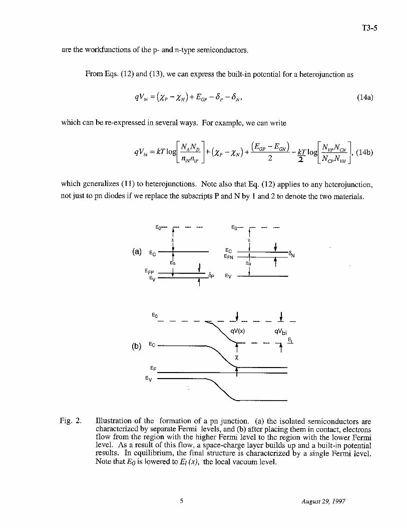
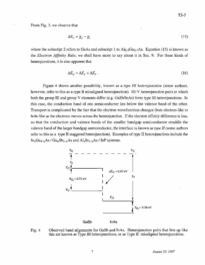
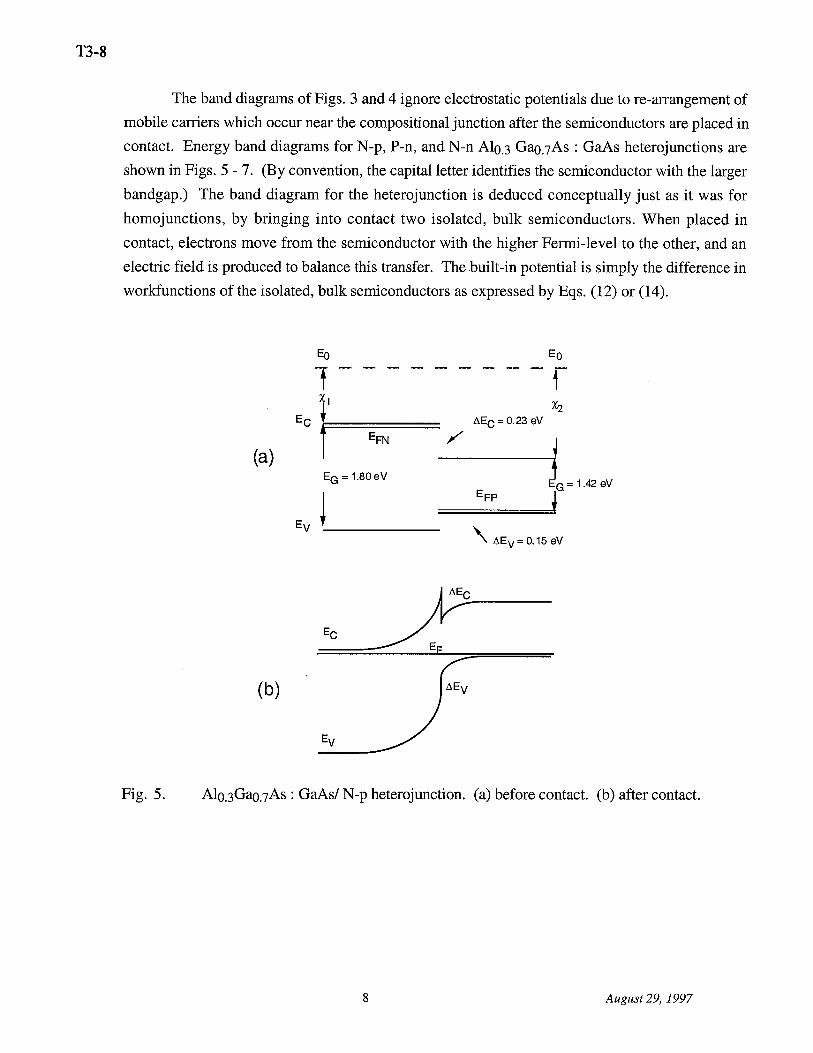
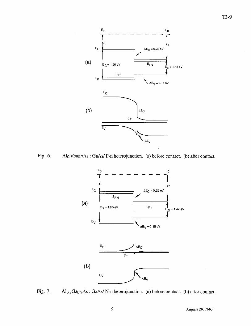
Upload buidang
View 238
Download 0
Embed Size (px) 344 x 292 429 x 357 514 x 422 599 x 487
Citation preview
Dec. 2011 - HBTS News
Nobel Lecture: The double heterostructure concept and its
Vertical Heterostructure of Two-Dimensional MoS and WSe ... · Vertical Heterostructure of Two-Dimensional MoS2 and WSe2 with ... vertical heterostructure of n-type MoS 2 and p-type
InP-based HBTs: Devices and GHz mixed-signal ICs
Facile one-pot synthesis of heterostructure SnO2/ZnO
Jan. 2012 - HBTS News
SiGe HBTs and BiCMOS Technology for Present and Future
Light-Emitting Heterostructure Thyristors
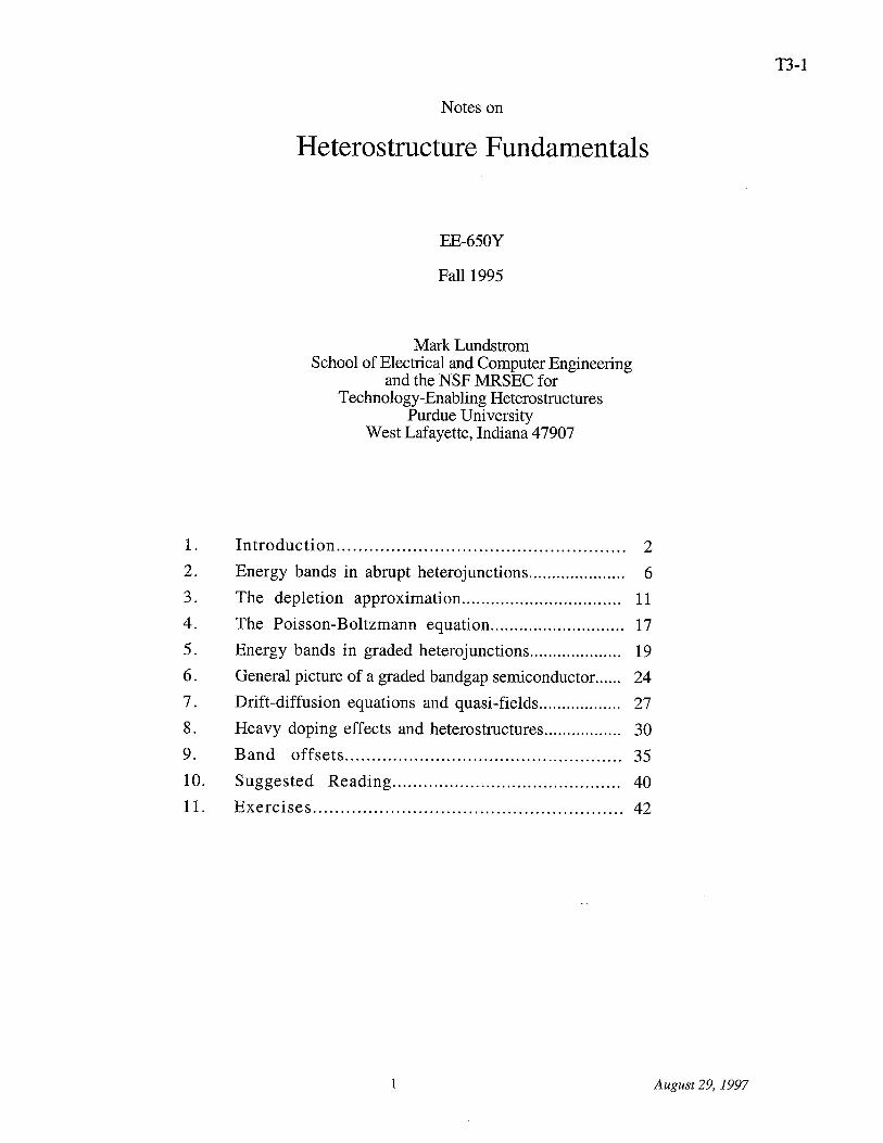
Heterostructure Fundamentals - nanoHUBheterostructurefundamentals.pdf · 1 February 25, 2013 Notes on Heterostructure Fundamentals EE-650Y Fall 1995 (Revised June 20, 2003, January
Feb. 2012 - HBTS News
SILICON/SILICON-GERMANIUM HETEROSTRUCTURE TUNNEL DIODES
InP-based HBTs: Devices and GHz mixed-signal ICs...Rodwell, short course, 2002 IEEE/OSA Conference on Indium Phosphide and Related Materials, May, Stockholm InP-based HBTs: Devices
3 Oxide Heterostructure Project - KEK
May 2012 HBTS News
dimensional van der Waals heterostructure devices ... · Supplementary Data Tunneling-based rectification and photoresponsivity in two-dimensional van der Waals heterostructure devices
& MoSe Lateral (6, Heterostructure 7KLV 2
Heterostructure Silicon (including Lecture-Tutorial-Laboratory Modules)
2001 Heterostructure Integrated Thermionic Cooling of
Planar Heterostructure Barrier Varactor Diodes for ...publications.lib.chalmers.se/records/fulltext/879/879.pdfThesis for the degree of Doctor of Philosophy Planar Heterostructure
Black Phosphorus and Phosphorene/Graphene Heterostructure
ACODINGSCHEMEFORWIRELESSNETWORKS WITHMULTIPLE …authors.library.caltech.edu/13767/1/OGGicassp07a.pdfA2 = diag(l,1,T3,T3,T3,T3), A3 = 1,T3,T3,T3,T3), andtheinitial transmitted signal
Sept. 2012 HBTS News
Models.semicond.gan Double Heterostructure Led
Process Technologies For Sub-100-nm InP HBTs & InGaAs MOSFETs
Nov. 2011 - HBTS News
Single-heterostructure laser diode producing a 6 W 40 ps ...pvlab.ioffe.ru/pdf/2012/Lanz1.pdf · Single-heterostructure laser diode producing a 6 W∕40 ps optical pulse ... Single-heterostructure
Effect of heterostructure engineering on electronic
Investigation of Novel Semiconductor Heterostructure ...thesis.library.caltech.edu/2373/1/master_final.pdfInvestigation of Novel Semiconductor Heterostructure Systems: I: Cerium Oxide/Silicon
HETEROSTRUCTURE BARRIER VARACTOR MULTIPLIERSamsacta.unibo.it/189/1/GAAS_5_1.pdf · HETEROSTRUCTURE BARRIER VARACTOR MULTIPLIERS ... The Heterostructure Barrier Varactor (HBV) diode
Novel Heterostructure Metal-Semiconductor-Metal (HMSM