Embed Size (px)
Citation preview
SYNTHESIZATION OF NOBLE METAL
NANOPARTICLES BY PULSED LASER
ABLATION METHOD IN LIQUIDS AND
THIN FILM APPLICATIONS
A THESIS
SUBMITTED TO THE MATERIALS SCIENCE AND
NANOTECHNOLOGY PROGRAM
AND THE GRADUATE SCHOOL OF ENGINEERING AND SCIENCES
OF BILKENT UNIVERSITY
IN PARTIAL FULLFILMENT OF THE REQUIREMENTS
FOR THE DEGREE OF
MASTER OF SCIENCE
By
Hüseyin Avni VURAL
September, 2012
ii
I certify that I have read this thesis and that in my opinion it is fully
adequate, in scope and in quality, as a thesis for the degree of Master of
Science.
Assist. Prof. Dr. Bülend Ortaç (Advisor)
I certify that I have read this thesis and that in my opinion it is fully
adequate, in scope and in quality, as a thesis for the degree of Master of
Science.
Assist.Prof. Dr. Ali Kemal Okyay
I certify that I have read this thesis and that in my opinion it is fully
adequate, in scope and in quality, as a thesis for the degree of Master of
Science.
Assoc.Prof.Dr. Hakan Altan
Approved for the Graduate School of Engineering and Sciences:
Prof.Dr. Levent Onural
Director of the Graduate School
iii
ABSTRACT
SYNTHESIZATION OF NOBLE METAL
NANOPARTICLES BY PULSED LASER
ABLATION METHOD IN LIQUIDS AND
THIN FILM APPLICATIONS
Hüseyin Avni VURAL
M.S. in Materials Science and Nanotechnology
Supervisor: Assist.Prof. Dr. Bülend Ortaç
September, 2012
Pulsed Laser Ablation in Liquid (PLAL) is promising, alternative,
easy, fast and free of agent method for synthesization of nanoparticles
(NPs). Various kinds of NPs can be synthesized easily by PLAL, such
as base metals, noble metals, semiconductors, nanoalloys, magnetic
and core–shell nanostructures. Additionally, crystallized NPs can be
easily obtained in one-step procedure by PLAL without subsequent
heat-treatments. Synthesization of gold (Au), silver (Ag) and platinum
(Pt) NPs with PLAL using Nd: YLF laser (Q-Switched Laser, 527 nm
wavelength, 16 W average power, 110 ns pulse duration, and 16 mJ
pulse energy for 1 kHz) in different liquid environments is reported.
Firstly, Ag, Au and Pt NPs have been synthesized with pulsed Nd:
YLF laser in deionized water. Secondly, these NPs have been
synthesized in methanol under similar conditions. Colloidal NP
solutions are then characterized with Transmission Electron
Microscopy, Scanning Electron Microscopy, X-Ray Photoelectron
Spectrophotometer, X-Ray Diffractometer and UV-Vis
Photospectrometer analysis techniques.
iv
In the second part, applications of noble metal nanoparticles have been
investigated. Firstly, Au and Ag NPs have been synthesized in
Polyvinylpyrolidone solution in order to prepare nanofibrous
composites. The Au and Ag NPs embedded in nanofibrous composites
then characterized with UV-Vis Photospectrometer and Transmission
Electron Microscopy. In addition, AuNPs have been synthesized with
varying energies of laser (9,2 mJ, 12 mJ and 16 mJ for 1kHz) in order
to understand the role of laser energy on PLAL. Finally, thin-film
applications also presented: Pulsed Laser Deposition by PLAL and
simple spin-coating deposition with AuNPs synthesized in methanol.
Keywords: Pulsed Laser Ablation Method, Gold, Silver and Platinum
Nanoparticles, Pulsed Laser Deposition, Thin Film Deposition, Optical
Characterization, Transmission Electron Microscopy, X-Ray
Photoelectron Spectroscopy, X-Ray Diffractometer.
v
ÖZET
SOY METAL NANOPARÇACIKLARIN
DARBELİ LAZER ABLASYON
YÖNTEMİYLE SIVILARDA ÜRETİMİ VE
İNCE FİLM UYGULAMALARI
Hüseyin Avni Vural
Malzeme Bilimi ve Nanoteknoloji, Yüksek Lisans
Tez Yöneticisi: Yrd. Doç. Dr. Bülend Ortaç
Eylül, 2012
Sıvı içerisinde Darbeli Lazer Ablasyon gittikçe gelişen, diğer
nanoparçacık üretim tekniklerine alternatif olabilecek, kolay, hızlı ve
başka bir kimyasal ajan gerektirmeyen nanoparçacık üretim
tekniklerinden biridir. Bu teknik ile baz metal, yarıiletken, manyetik
nanoparçacıklar ile alaşım halinde veya çekirdek-kabuk şeklinde olan
nano yapılar üretilebilinir. Kristal nanoyapıları ısı işlemi gerektirmeden
tek bir adım ile elde etmek mümkündür. Altın, gümüş ve platin
nanoparçacıkların Nd: YLF lazer (Q-Anahtarlama, 527 nm dalga boyu,
16 W ortalama güç, 110 ns darbe süresi, ve 1 kHz için 16 mJ darbe
enerjisi) sistemi kullanılarak deiyonize su ve metanol sıvıları içerisinde
Darbeli Lazer Ablasyon yöntemi ile üretimi rapor edilmiştir. Geçirgen
Elektron Mikroskobu, Taramalı Elektron Mikroskobu, X-Işınlı
Fotoelektron Spektroskopisi, X-Işınlı Kırınım Ölçer ve Morötesi /
Görünür Bölge Spektroskopisi ile oluşturulan koloidal nanoparçacık
sıvıların karakterizasyonları sunulmuştur. Tezin ikinci bölümünde, soy
metal nanoparçacıkların uygulamalarına örnek olarak ilk başta altın ve
gümüş nanoparçacıklar polimer bir sıvı olan Polyvinylpyrolidone
vi
içinde nanofiber yapılarda kullanılmak için sentezlenmiştir. Elde edilen
nanofiberler içerisine gömülü nanoparçacıklar Taramalı Elektron
Mikroskobu ve Morötesi / Görünür Bölge Spektroskopisi ile
karakterize edilmiştir. Lazer enerjisinin Darbeli Lazer Ablasyon’da ki
rolünü anlamak için lazerin ortalama enerjisi 9,2mJ, 12 mJ ve 16 mJ
olarak değiştirilerek deiyonize su içerisinde altın nanoparçacıklar elde
edilmiş ve karakterize edilmiştir. Bu uygulamalara ek olarak, cam
örnek üzerine sıvı içinde Darbeli Lazer Kaplama tekniği ile film
büyütülmesi ve nanoparçacık sıvıdan ince film kaplama yapılması ele
alınmıştır.
Anahtar Sözcükler: Darbeli Lazer Ablasyon, Altın, Gümüş ve Platin
Nanoparçacıklar, Darbeli Lazer Kaplama, İnce Film, Optiksel
Karakterizasyon, Geçirgen Elektron Mikroskobu, X-Işınlı Fotoelektron
Spektroskopisi, X-Işınlı Kırınım Ölçer.
vii
Acknowledgement
I would like to express my deepest gratitude to my supervisor Dr.
Bülend Ortaç and the Director of Graduate Program of Materials
Science and Nanotechnology, Dr. Salim Çıracı for their valuable
guidance, support and encouragement. I would like to thank UNAM
engineers; Enver Kahveci, Mustafa Güler, and Adem Saraç for their
great help for XRD, XPS, TEM and SEM measurements. I would also
like to thank my group member Salamat Burzhuev and UNAM Uyar
Research Group members; Dr. Tamer Uyar and Ali Ekrem Deniz.
I would like to thank my colleagues Hulusi Birol Bilgili, Yunus Ataş
and Merve Çelikbudak from ROKETSAN for their support and
guidance. My appreciation goes to Elif Ünal for editing and reading the
thesis carefully.
I wish to give my special thanks to my parents and friends for their
help, support and patience.
The financial support from UNAM and SANTEZ is also gratefully
acknowledged.

viii
Dedicated to my lovely Grandmother
ix
Contents
1. Introduction ............................................................................................ 1
1.1 Nanotechnology & Nanomaterials ................................................... 1
1.2 The Synthesis of Nanoparticles ....................................................... 2
1.2.1 Top-down method .................................................................... 2
1.2.2 Bottom-up method ................................................................... 2
1.3 Nanoparticle Synthesis Techniques ................................................. 3
1.4 Pulsed Laser Ablation Method ......................................................... 3
1.5 Noble Metal Nanoparticles .............................................................. 5
1.6 Optical, Thermal and Catalytic Properties of Noble Metal
Nanoparticles ............................................................................................... 5
2. The Formation Mechanism of Nanoparticles .................................... 10
2.1 Pulsed Laser Ablation Method in Gas ........................................... 11
2.2 Pulsed Laser Ablation Method in Liquid ....................................... 11
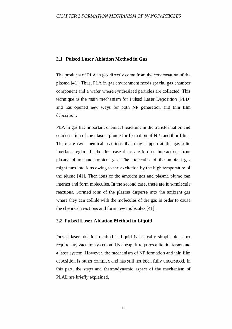
2.2.1 The evolution of pulsed laser ablation in liquid ..................... 12
2.2.2 Nucleation thermodynamics .................................................. 13
2.2.3 Kinetic growth ....................................................................... 15
3. Experimental Results and Discussions ............................................... 18
3.1 Gold, Silver and Platinum Nanoparticle Synthesis in Water ......... 19
3.2 Gold, Silver and Platinum Nanoparticle Synthesis in Methanol .... 32
3.3 Gold and Silver Nanoparticles Synthesis in Polymeric Solution ... 45
3.4 Gold Nanoparticle Synthesis in Water with Different Average
Powers ....................................................................................................... 48
3.5 Gold Thin Film Deposition on Glass Substrate ............................. 54
3.6 Gold thin film deposition with spin coating................................... 57
4. Conclusion ............................................................................................ 58
Bibliography ................................................................................................. 60
x
List of Figures
Figure 1-1. Absorption spectrum various sizes and shapes of AuNPs.
Adopted from [34]. 7
Figure 1-2. Relation of melting point and radius of Au Nanoparticles [36]. 8
Figure 2-1. The evolution of PLA mechanism in liquid. 13
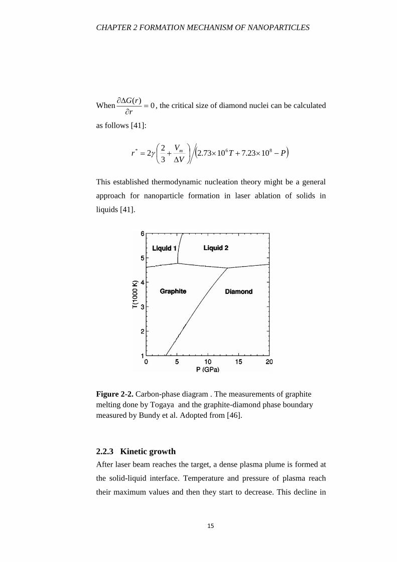
Figure 2-2. Carbon-phase diagram . The measurements of graphite melting
done by Togaya and the graphite-diamond phase boundary measured by
Bundy et al. Adopted from [46]. 15
Figure 2-3. The Relation between nucleation time and pressure. Adopted
from [41]. 17
Figure 3-1. Experimental scheme of PLAL. 18
Figure 3-2. Picture Ag, Au, and Pt NPs synthesized in water. 20
Figure 3-3. SEM pictures of Au, Ag, PtNPs in Water a) AgNPs, b) AuNPs, c)
PtNPs. 21
Figure 3-4. XPS studies of Ag, Au, Pt NPs on Silicon Wafer. a) XPS
Spectrum of AgNPs after etching b) XPS Spectrum of AuNPs after etching c)
XPS Spectrum of PtNPs after etching. 23
Figure 3-5. XRD studies of Ag, Au and Pt NPs. a) Ag NPs, b) Au NPs, c) Pt
NPs. 25
Figure 3-6. Absorption studies of Au, Ag, and Pt NPs. a) Ag NPs, b) Au NPs,
c) Pt NPs. 27
Figure 3-7. TEM studies of Au NPs. a) General image and size distribution.
b) HRTEM image of Au NP: Atomic planes of Au NP. 29
Figure 3-8. TEM studies of Ag NPs. a) General image and size distribution.
b) HRTEM image of Ag NP: Atomic planes of Ag NP. 30
Figure 3-9. TEM studies of Pt NPs. a) General image and size distribution. b)
HRTEM image of Pt NP: Atomic planes of Pt NP. 31
Figure 3-10. Picture of Ag, Au and Pt NPs. 32
Figure 3-11. SEM pictures of Au, Ag, Pt NPs in Methanol a) Ag NPs, b) Au
NPs, c) Pt NPs. 34
Figure 3-12. XPS studies of Au, Ag, Pt NPs in Methanol a) Ag NPs, b) Au
NPs, c) Pt NPs. 36
xi
Figure 3-13. XRD graphs of Au, Ag, Pt NPs in Methanol a) Ag NPs, b) Au
NPs, c) Pt NPs. 38
Figure 3-14. Absorption studies of Au, Ag, and Pt NPs. a) Ag NPs, b) Au
NPs, c) Pt NPs. 40
Figure 3-15. TEM studies of Au NPs in methanol. a) General image and size
distribution. b) HRTEM image of Au NP: Atomic planes of Au NP. 42
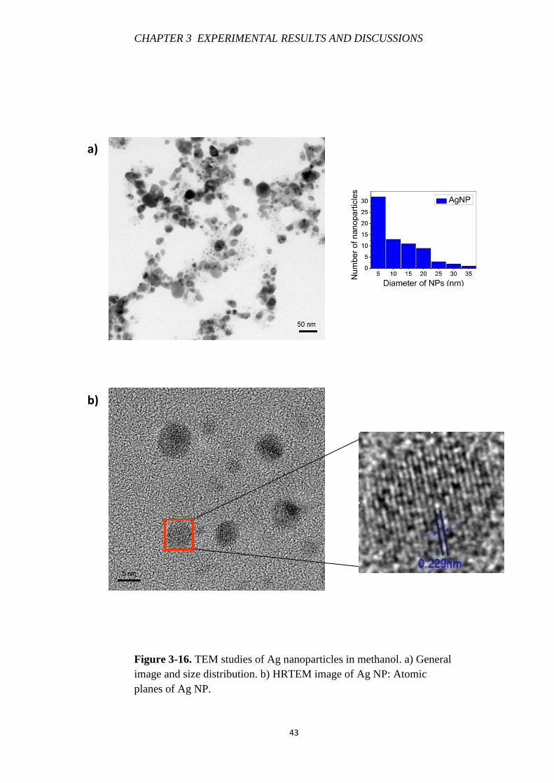
Figure 3-16. TEM studies of Ag nanoparticles in methanol. a) General image
and size distribution. b) HRTEM image of Ag NP: Atomic planes of Ag NP.
43
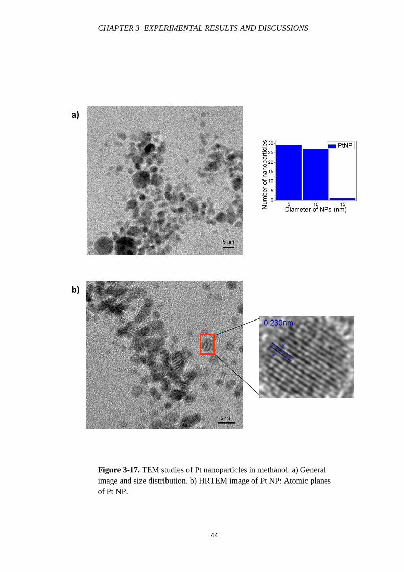
Figure 3-17. TEM studies of Pt nanoparticles in methanol. a) General image
and size distribution. b) HRTEM image of Pt NP: Atomic planes of Pt NP. 44
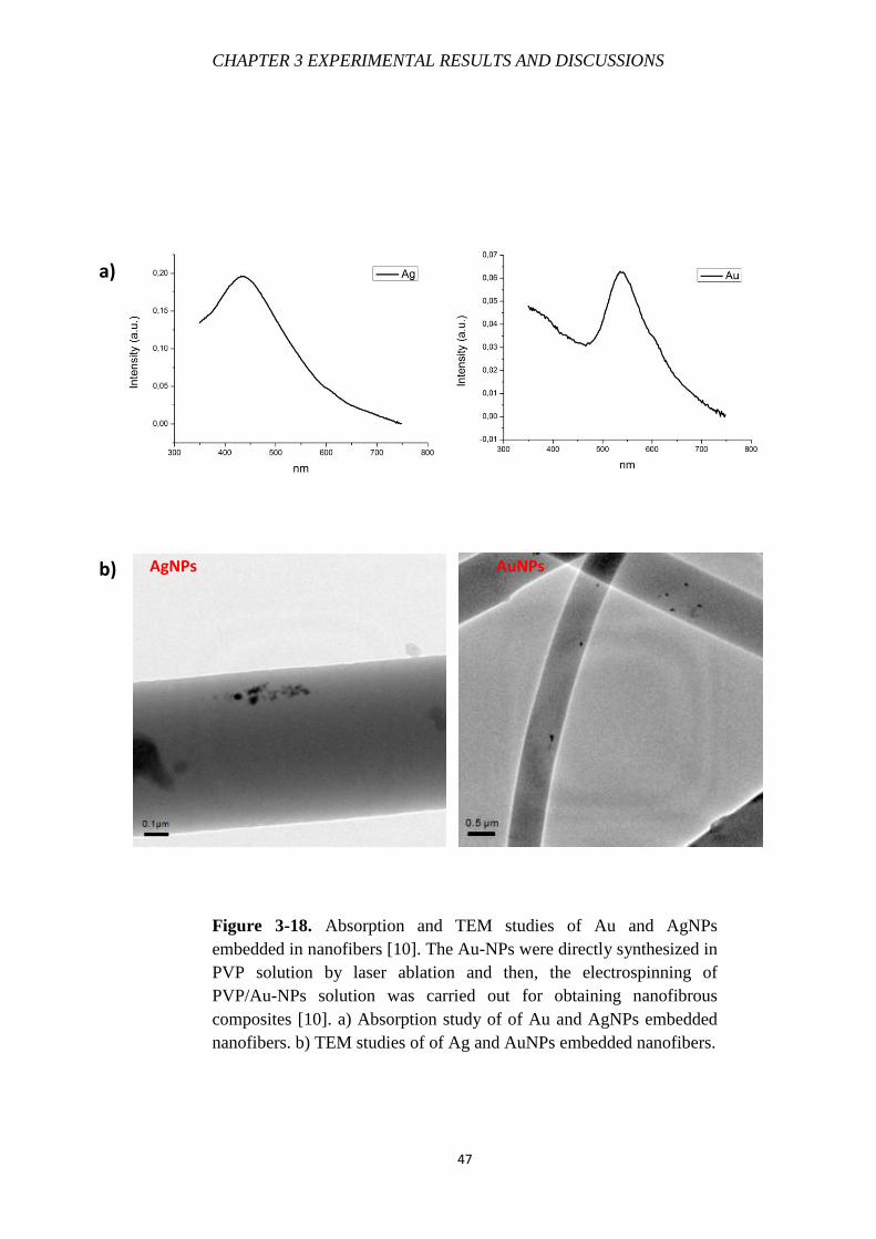
Figure 3-18. Absorption and TEM studies of Au and AgNPs embedded in
nanofibers [10]. The Au-NPs were directly synthesized in PVP solution by
laser ablation and then, the electrospinning of PVP/Au-NPs solution was
carried out for obtaining nanofibrous composites [10]. a) Absorption study of
of Au and AgNPs embedded nanofibers. b) TEM studies of of Ag and AuNPs
embedded nanofibers. 47
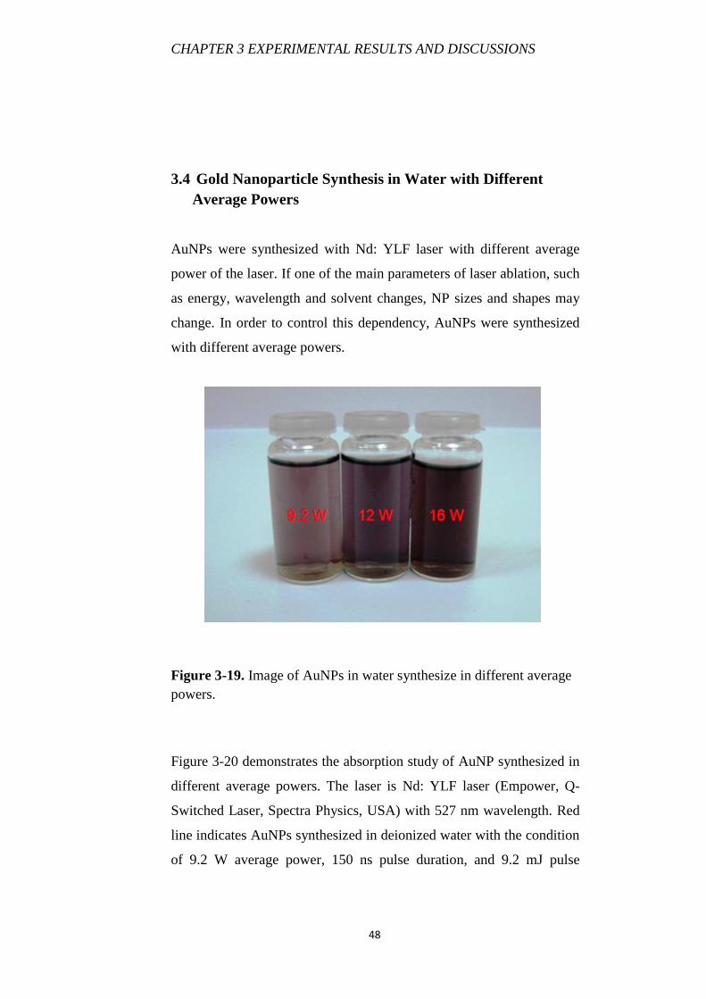
Figure 3-19. Image of AuNPs in water synthesize in different average
powers. 48
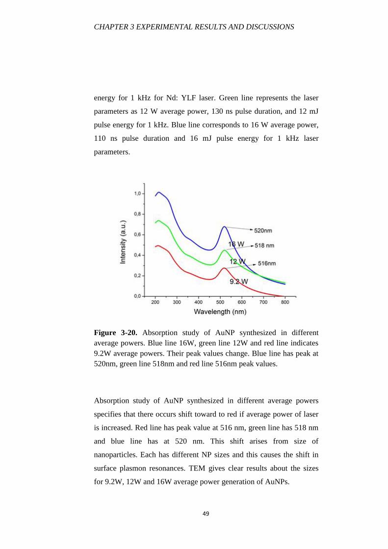
Figure 3-20. Absorption study of AuNP synthesized in different average
powers. Blue line 16W, green line 12W and red line indicates 9.2W average
powers. Their peak values change. Blue line has peak at 520nm, green line
518nm and red line 516nm peak values. 49
Figure 3-21. TEM studies of AuNPs synthesized in 527nm, 9.2 W, 150 ns
Nd:YLF laser in water. General image and size distribution corresponding to
the image. 51
Figure 3-22. TEM studies of AuNPs synthesized in 527nm, 12 W, 130 ns
Nd:YLF laser in water. General image and size distribution corresponding to
the image. 52
Figure 3-23. TEM studies of AuNPs synthesized in 527nm, 16 W, 110 ns
Nd:YLF laser in water. General image and size distribution corresponding to
the image. 53
Figure 3-24. Schematic view of gold thin film deposition on glass by pulsed
laser ablation in liquid technique 54
Figure 3-25. Picture of Au deposited glass substrate. 54
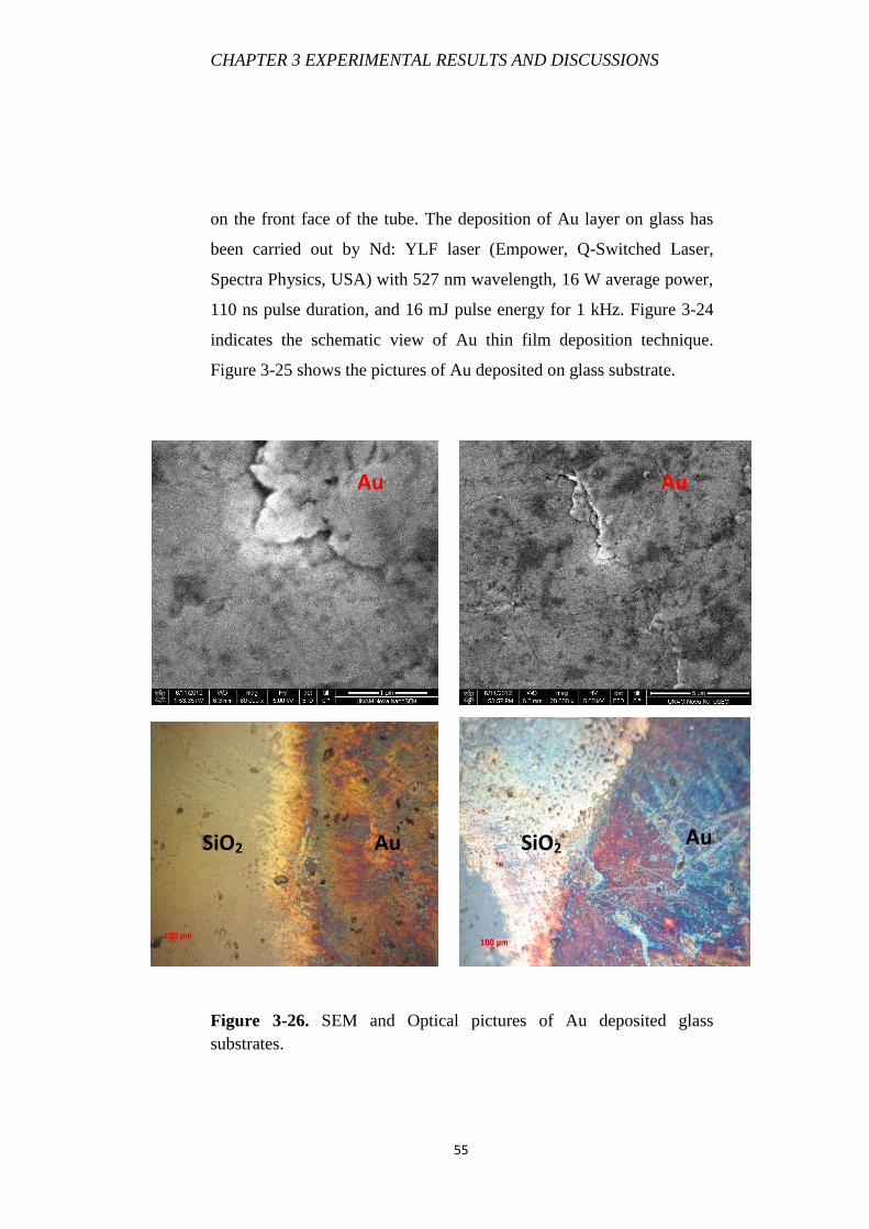
Figure 3-26. SEM and Optical pictures of Au deposited glass substrates. 55

xii
Figure 3-27. XPS Studies of Au deposited glass substrate. 56
Figure 3-28. SEM picture and EDX analysis of Au deposited thin film. 57
xiii
List of Symbols/Abbreviations/Acronyms
NP - Nanoparticle
NPs - Nanoparticles
NMNP - Noble Metal
Nanoparticle
NMNPs - Noble Metal
Nanoparticles
PLA - Pulsed Laser Ablation
PLAL - Pulsed Laser Ablation
in Liquids
Au – Gold
Ag – Silver
Pt – Platinum
Cu- Copper
AuNP - Gold Nanoparticle
AuNPs – Gold Nanoparticles
AgNP - Silver Nanoparticle
AgNPs – Silver Nanoparticles
PtNP - Platinum Nanoparticle
PtNPs – Platinum
Nanoparticles
UV- Ultraviolet
DVD - Digital Versatile Discs
Vis - Visible
NaBH4 - Sodium Borohydride
PLD - Pulsed Laser Deposition
SPR - Surface Plasmon
Resonance
LSPR – Localized Surface
Plasmon Resonance
XPS - X-Ray Photoelectron
Spectroscopy
XRD - X-Ray Diffractometer
SEM - Scanning Electron
Microscope
EDX- Energy Dispersive X-
Ray
TEM - Transmission Electron
Microscope
Nd: YLF - Neodymium-doped
yttrium lithium fluoride (Nd:
LiYF4)
Nd: YAG - Neodymium-doped
yttrium aluminum garnet
(Nd:Y3Al5O12)
a.u. - arbitrary unit
fcc - face-centered cubic
PVP- Polyvinylpyrolidone
nm – nanometer
cm - centimeter
CHAPTER I INTRODUCTION
1
Chapter 1
1. Introduction
1.1 Nanotechnology & Nanomaterials
Basic advancements in science and technology may arise twice in a
century and lead to a massive wealth creation. For instance, textile
which left its place to railroads and automobiles in the 20th
century,
was the main technology in 19th century. Today, we use computer-
oriented technology being estimated to last till 2025. Nanoscience and
Nanotechnology will be one of the future possible dominant
technologies in the 21st century and we are just at the beginning [1].
The new technology starts with the famous speech of Richard
Feynman; “There is Plenty of Room at the Bottom”, claiming that 24
volumes of Encyclopedia Britannica can be written on the head of a
pin. If Feynman had been justified, even all books in The Library of
Congress, British Museum Library and National Library in France
could have been as small as three square yards (two and a half meter
square) [2]. Today, we experience that he is right! Recent technological
devices such as, Digital Versatile Discs (DVDs), notebooks, smart
phones, textile products and many other electronic devices use
nanotechnology. These new advancements are the only visible part of
an iceberg and the influence of nanotechnology will be felt more in all
areas of our daily lives in the future. Basically, nanotechnology deals
with processes taking place at the nanometer scale that is,
approximately 1 to 100 nm. Nanoparticle (NP) is a particle whose three
CHAPTER I INTRODUCTION
2
dimensions are 1 to 100 nm exists in diverse shapes such as spherical,
triangular, cubical, pentagonal, rod-shaped, shells, ellipsoidal and so
forth [3]. Moreover, NP has a higher surface to volume ratio and
increased percentage of atoms at the grain boundaries giving it
distinctive features and enabling it to have unique optical, catalytic,
and electrical properties [3]. These properties make NPs so important
in nanotechnology that it is used in various applications such as
surface-enhanced Raman spectroscopy [4], nanophotonics devices [5],
drug delivery [6], solar cells [7], catalysis [8], sensor [9] and
nanotextile [10].
1.2 The Synthesis of Nanoparticles
1.2.1 Top-down method
Top-down method is essentially the breaking down of a system into its
subsystems. It can be exemplified as constructing a building or a statue
by shaping a rock. The top-down approach often uses cutting, milling
or drilling tools to get smaller components. Micropatterning techniques
such as, photolithography, plasma etching and laser ablation can be
classified under this method.
1.2.2 Bottom-up method
Bottom-up method is uniting of smaller components to comprise larger
systems. It can be represented as constructing a building by uniting
bricks or assembling the parts of a car engine. In biotechnology,
bottom–up method is used to get biotechnological components by
combining single molecules. In nanotechnology, it can be defined as
self-assembly of atoms and molecules to form larger systems.
Chemical vapour deposition (CVD) and sol-gel process can be
classified under this method.
CHAPTER I INTRODUCTION
3
1.3 Nanoparticle Synthesis Techniques
A number of techniques can be used for NP preparation. Some
examples are chemical reduction [11], photo-reduction [12], flame
metal combustion [13], electrochemical reduction [14], solvothermal
[15], electrolysis [16], chemical fluid deposition [17], and spray
pyrolysis [18]. The standard method to obtain Noble Metal
Nanoparticles (NMNPs) is chemical reduction of metal salts in the
presence of stabilizing molecules [19]. The citrate reduction method in
aqueous solution and the NaBH4 reduction method are the most
popular methods for synthesis of NMNPs [19]. In addition, the pulsed
laser ablation in liquids (PLAL) has become an increasingly popular
top-down approach for producing NPs. PLAL has been a relatively
new method that was first introduced by Fojtik et al. in 1993 [20] and
has become increasingly popular top-down approach method.
1.4 Pulsed Laser Ablation Method
Pulsed laser ablation (PLA) has been used since the invention of the
pulsed ruby laser in 1960 by T.H.Maiman [21]. Soon after this
invention, Brech and Cross used ruby maser to observe the scattering
of light from metal surface and it was the first time of laser-material
interaction [22]. First studies about PLA were performed in diluted gas
and vacuum environments in the late 80s. The first study of PLA at the
solid-liquid interface was reported by Patil and his co-workers in 1987
[23]. Patil and his co-workers synthesized metastable form of iron
oxide using high power pulsed laser in liquid [23]. Basically, PLA has
three alternative techniques according to its environment; vacuum, gas
and liquid. Among them, liquid environment is the newest one
CHAPTER I INTRODUCTION
4
compared to the others and has received much attention as an original
NP production technique.
PLAL has many individual advantages over other NP synthesization
methods. First of all, it is chemically free of agents and the
experimental set-up is cheap provided that laser is available and has
easily controlled parameters. Secondly, various kinds of NPs can be
synthesized easily by PLAL, such as metals [24], noble metals [10],
semiconductors [25], nanoalloys [26], magnetic [27] and core–shell
nanostructure [28]. Additionally, crystallized NPs can be easily
obtained in one-step procedure by PLAL without subsequent heat-
treatments [10]. These advantages allow a designer to use number of
choices of different targets and liquids corresponding to the desired
parameters of synthesis.
Solvents, pulse duration and power of a laser are parameters of PLAL.
Provided that one of these parameters changed, the size and shape of
nanoparticles could be changed. For instance, AuNPs synthesized in
water consist of 8 nm diameter (64% standard deviation), if a 1064-nm
wavelength, 9 nanosecond pulse duration and 10-20 Joule/cm-2
fluence
is used [19]. On the other hand, they have 4-130 nm diameters when
800 nm wavelength, 120 femtosecond pulse duration and 60-1000
Joule/cm-2
fluence is used [19].
If the solvent changes, all thermodynamic relation between liquid and
target changes as well. For instance, AgNPs have diameter of 7.8 nm
(with 49% standard deviation) in Dimethylsulfoxide, 4.8 nm (with 46%
standard deviation) in Tetrahydrofuran and 3.8 nm (with 79% standard
deviation) in Acetonitrite when 1064 nm wavelength, 9 nanosecond
pulse duration and 10 Joule/cm-2
laser fluence is used [19].
CHAPTER I INTRODUCTION
5
1.5 Noble Metal Nanoparticles
Gold, Silver, Mercury, Platinum, Iridium, Palladium, Osmium,
Rhodium, and Ruthenium are known as noble metals and show high
resistivity to oxidation and corrosion even at high temperatures and
these features make them precious metals. These metals show
distinctive physical and chemical properties different from the most
base metals and lead to use noble metals as a “nanoparticles” in
nanotechnology. NMNPs are widely used and applicable in
nanotechnology due to the existence of localized plasmonic modes in
the visible–near infrared interval, the easy surface functionalization and
the chemical and physical stability [19]. These features of NMNp have
attracted great attention in the field of optoelectronics, biotechnology,
chemical applications. The number of publications on NMNPs shows
exponential growing and thus they are indispensable and the basis for
the most of the applications on nanotechnology [3].
1.6 Optical, Thermal and Catalytic Properties of Noble
Metal Nanoparticles
Optical properties, such as optical emission and absorption, purely
depend on transition between valence band and conduction band.
Noble metals, similar to other metals, do not have their electrons on
bounded. There is a cloud around the atomic core and thus they
become good conductors. This unique property also affects optical
properties. When a photon with certain wavelength comes onto this
cloud, photon can be absorbed and oscillations in the electron cloud are
produced. This phenomenon is formed on the surface of metals thereby
CHAPTER I INTRODUCTION
6
it is called Surface Plasmon Resonance. Other photons with various
wavelengths can be reflected and may not get in oscillation.
The penetration depth of Electromagnetic (EM) waves in metal is at the
order of 30 nm [3]. Provided that the diameter of a NP is smaller than
30 nm, the EM waves can propagate through the particle. These EM
waves drive conduction band electrons as a group according to the
fixed positive lattice ions [3]. Eventually, a net charge difference
occurs on the surface of nanoparticle [3].These charges form an
oscillating dipole and radiate EM waves. The radiated EM waves are
known as Localized Surface Plasmon Resonance (LSPR). If some of
the photons are released with the same frequency in all directions, this
process is called scattering. If some of the photons are converted into
phonons or vibrations of the lattice, this process is referred to as
absorption [3].
If the diameter of a particle gets smaller the energy required to
collectively excite motion of the surface plasmon electrons increases
[29]. If the shape of the particles changes, same conditions occur. Thus,
we observe changes in plasmon resonances causing a difference in
absorption peaks. Moreover, on the condition that a surrounding
medium changes, the surface plasmon resonance band changes as well
due to the dielectric properties of the surrounding medium[30].
Surrounding medium with high refractive indices is much more
polarizable and thus couples with the surface plasmon electrons more
readily [31]. The energy required to excite the electrons collectively is
decreased [31]. The technique for measurement of SPR can be
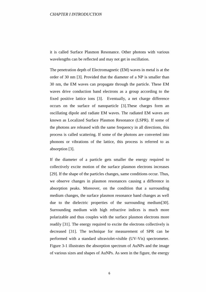
performed with a standard ultraviolet-visible (UV-Vis) spectrometer.
Figure 3-1 illustrates the absorption spectrum of AuNPs and the image
of various sizes and shapes of AuNPs. As seen in the figure, the energy
CHAPTER I INTRODUCTION
7
required to excite the surface plasmon of Au NPs with diameters near 5
nm is comparable to the energy of visible light [31].
NMNPs are used for their LSPR in some fields. Here are some
examples:
The molecule-specific imaging and diagnosis of diseases such
as cancer can be carried out by means of the strong LSPR
scattering of AuNPs conjugated with specific targeting
molecules [32].
Nanorods or nanoshells of Au have LSPR is in the near-infrared
region. Hence, they can be used in vivo imaging and therapy
[32].
Nonspherical plasmon resonant NMNPs offer favorable
properties for their use as analytical tools, transport vehicles, as
well as diagnostic and therapeutic agents [33].
Figure 1-1. Absorption spectrum various sizes and shapes of AuNPs.
Adopted from [34].
CHAPTER I INTRODUCTION
8
Figure 1-2. Relation of melting point and radius of Au Nanoparticles
[36].
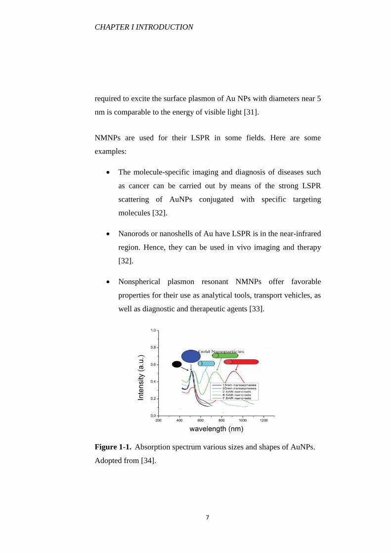
A large increase in the surface area of NPs has a significant effect on
material properties as well. For instance, the melting point of AuNPs
can decrease significantly for particle sizes less than 10 nm [35].
Figure 1-2 shows the relation of melting point and radius of AuNPs. It
is clear from the figure that the melting point of AuNPs with smaller
sizes than 10 nm decreases sharply.
The exposed surface is the only active area for catalytic properties of
any materials because inner atoms do not interact with substrates [37].
Therefore, NPs can be better candidates for catalytic reactions instead
of bulk ones. Noble metals, especially Pt, are known as good catalysts
and they are deeply studied and used for catalytic applications.
Although they are very efficient for speeding up reactions, they are
very expensive and the price of Pt limits the use of these materials as a
catalyst. Therefore, smaller particles are required for cost efficiency.
For instance, a Au particle with 20 nm diameter contains 384.000
CHAPTER I INTRODUCTION
9
atoms, while a 3-nanometer particle contains 300 times fewer atoms
almost 1.300 atoms [37]. Assuming the both AuNP as a sphere, we can
calculate their surface area. A 20-nm AuNP has 1256 nm 2 surface area
on the other hand a 3-nm AuNP has 28.27 nm 2 surface area. We realize
300 times fewer atoms at a 3-nm AuNP but the surface area is about 44
times less. The smaller particles we get the more efficient catalysts we
obtain. Therefore, more effective and low-cost catalyst can be
generated by increasing active area interacting with substrate and
decreasing the volume of the catalyst. Although smaller NPs are more
effective and cheaper as a catalyst, it is inevitable to face some
drawbacks. For instance, a PtNP with 2 nm produces water for the
synthesis of hydrogen peroxide and limits our cost-efficiency problem
[37]. As a result, the controlling size of NPs eliminates the waste and
supply for only desired products.
NMNPs are used for their catalytic properties. Here are some
examples:
Bulk Au is inert and has often been thought as poorly active for
catalytic reactions. However, when AuNPs diameters are below
10 nm, it turns out to be surprisingly active for many reactions,
such as CO oxidation and propylene epoxidation [38].
AgNPs located at a graphene edge catalyze oxidation of
neighboring carbon atoms [39].
Well-dispersed PtNPs are an important catalyst for fuel-cell
reactions [40].

CHAPTER 2 FORMATION MECHANISM OF NANOPARTICLES
10
Chapter 2
2. The Formation Mechanism of Nanoparticles
When the laser beam reaches the surface of target, the energy of the
photons in the laser beam is transferred into electrons and then into the
lattice, diffusing the energy into the material afterwards [3]. Laser
beam focusing on the surface of the material may be in the order of
micron levels which heat the surface in a way that it reaches a critical
temperature and causes rapid vaporization process [3]. This rapid
vaporization forms ionized atoms and electrons i.e.; plasma on the
target. On the condition that plasma has more energy with more laser
power, it can expand and then cool therefore particles on the order of
nanometer and micrometer begin to form.
Plasma is confined when it occurs in liquid environment apart from
vacuum and gas phases. As a result, a lot of different mechanisms
including generation, transformation, and condensation of plasma
plume in liquid are formed. These mechanisms are still not fully
understood. Some authors [41-45] have tried to explain these
mechanisms using thermodynamics rules and generalized them for all
particles using carbon-phase diagram.
.
CHAPTER 2 FORMATION MECHANISM OF NANOPARTICLES
11
2.1 Pulsed Laser Ablation Method in Gas
The products of PLA in gas directly come from the condensation of the
plasma [41]. Thus, PLA in gas environment needs special gas chamber
component and a wafer where synthesized particles are collected. This
technique is the main mechanism for Pulsed Laser Deposition (PLD)
and has opened new ways for both NP generation and thin film
deposition.
PLA in gas has important chemical reactions in the transformation and
condensation of the plasma plume for formation of NPs and thin-films.
There are two chemical reactions that may happen at the gas-solid
interface region. In the first case there are ion-ion interactions from
plasma plume and ambient gas. The molecules of the ambient gas
might turn into ions owing to the excitation by the high temperature of
the plume [41]. Then ions of the ambient gas and plasma plume can
interact and form molecules. In the second case, there are ion-molecule
reactions. Formed ions of the plasma disperse into the ambient gas
where they can collide with the molecules of the gas in order to cause
the chemical reactions and form new molecules [41].
2.2 Pulsed Laser Ablation Method in Liquid
Pulsed laser ablation method in liquid is basically simple, does not
require any vacuum system and is cheap. It requires a liquid, target and
a laser system. However, the mechanism of NP formation and thin film
deposition is rather complex and has still not been fully understood. In
this part, the steps and thermodynamic aspect of the mechanism of
PLAL are briefly explained.
CHAPTER 2 FORMATION MECHANISM OF NANOPARTICLES
12
2.2.1 The evolution of pulsed laser ablation in liquid
When a laser beam counters with the surface of a solid target in liquid,
plasma is generated. Then the surface of target is heated in a way that it
reaches critical temperature where causes rapid vaporization process
[3]. This rapid vaporization forms ionized atoms and electrons i.e.;
plasma on the target [3]. After plasma is formed, it initiates to react
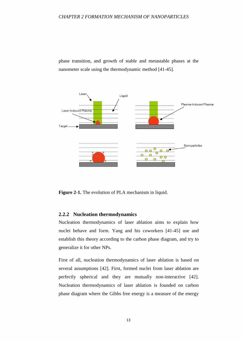
with liquid and it is schematically illustrated in Figure 2-1 . The figure
shows us the evolution of the laser ablation in liquid. First formed
plasma by laser beam is called "laser-induced plasma" and this is
illustrated in Figure 2-1.a. If the plasma is enlarged by laser-induced
plasma due to more energy provided by laser, it is called the plasma-
induced plasma [41]. In other words, firstly, laser causes plasma at
interface of liquid and solid then the formed plasma grow out and
larger plasma occurs. (Please see Figure 2-1.b.) After plasma-induced
plasma occurs, four chemical reactions arise inside the plasma and
interface layer of plasma and liquid, at nanoscale time range [41]. In
first stage, metastable phase can be formed by high temperature
chemical reactions inside the plasma [41]. Next, the second set of
reactions play a role where reactant species from target and liquid
begin to contact and affect each other. At the third part, these formed
reactant species get into high temperature chemical reactions with
molecules in liquid [41]. High pressure inside the plasma induced
plasma push the ablated species into liquid and this process is named as
the fourth phase [41]. After these four kinds of processes are
completed, cooling down and condensation in the confining liquid
starts and NPs begin to form.
The mechanisms involved in the nucleation, phase transition, and
growth of nanocrystals upon laser ablation in liquids are not fully
understood. A few papers have been reported to explain the nucleation,
CHAPTER 2 FORMATION MECHANISM OF NANOPARTICLES
13
phase transition, and growth of stable and metastable phases at the
nanometer scale using the thermodynamic method [41-45].
Figure 2-1. The evolution of PLA mechanism in liquid.
2.2.2 Nucleation thermodynamics
Nucleation thermodynamics of laser ablation aims to explain how
nuclei behave and form. Yang and his coworkers [41-45] use and
establish this theory according to the carbon phase diagram, and try to
generalize it for other NPs.
First of all, nucleation thermodynamics of laser ablation is based on
several assumptions [42]. First, formed nuclei from laser ablation are
perfectly spherical and they are mutually non-interactive [42].
Nucleation thermodynamics of laser ablation is founded on carbon
phase diagram where the Gibbs free energy is a measure of the energy
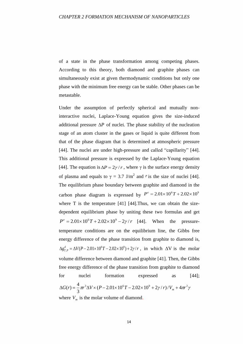
CHAPTER 2 FORMATION MECHANISM OF NANOPARTICLES
14
of a state in the phase transformation among competing phases.
According to this theory, both diamond and graphite phases can
simultaneously exist at given thermodynamic conditions but only one
phase with the minimum free energy can be stable. Other phases can be
metastable.
Under the assumption of perfectly spherical and mutually non-
interactive nuclei, Laplace-Young equation gives the size-induced
additional pressure P of nuclei. The phase stability of the nucleation
stage of an atom cluster in the gases or liquid is quite different from
that of the phase diagram that is determined at atmospheric pressure
[44]. The nuclei are under high-pressure and called “capillarity” [44].
This additional pressure is expressed by the Laplace-Young equation
[44]. The equation is rP /2 , where γ is the surface energy density
of plasma and equals to γ = 3.7 J/m2 and r is the size of nuclei [44].
The equilibrium phase boundary between graphite and diamond in the
carbon phase diagram is expressed by 96 1002.21001.2 TPe
where T is the temperature [41] [44].Thus, we can obtain the size-
dependent equilibrium phase by uniting these two formulas and get
rTPe /21002.21001.2 96 [44]. When the pressure-
temperature conditions are on the equilibrium line, the Gibbs free
energy difference of the phase transition from graphite to diamond is,
rTPVgd
PT /2)1002.21001.2( 96
, , in which V is the molar
volume difference between diamond and graphite [41]. Then, the Gibbs
free energy difference of the phase transition from graphite to diamond
for nuclei formation expressed as [44];
2963 4/)/21002.21001.2(3
4)( rVrTPVrrG m
where mV is the molar volume of diamond.
CHAPTER 2 FORMATION MECHANISM OF NANOPARTICLES
15
When 0)(
r
rG, the critical size of diamond nuclei can be calculated
as follows [41]:
PTV
Vr m
86* 1023.71073.2
3
22
This established thermodynamic nucleation theory might be a general
approach for nanoparticle formation in laser ablation of solids in
liquids [41].
Figure 2-2. Carbon-phase diagram . The measurements of graphite
melting done by Togaya and the graphite-diamond phase boundary
measured by Bundy et al. Adopted from [46].
2.2.3 Kinetic growth
After laser beam reaches the target, a dense plasma plume is formed at
the solid-liquid interface. Temperature and pressure of plasma reach
their maximum values and then they start to decrease. This decline in
CHAPTER 2 FORMATION MECHANISM OF NANOPARTICLES
16
the process is called as condensation of plasma which leads to the
formation of nanocrystals via growth of nuclei [41].
Assume the clusters and the surrounding plasma have the same
temperature T, then isothermal nucleation time is given by [41].
2))((
2
Tp
kTmkT
s
where m,k,T, , )(Tps , denote the mass of a single atom, the
Boltzmann's constant, the absolute temperature, the surface energy
density of diamond, saturated vapor pressure of nuclei at the
temperature of T and atom chemical potential difference respectively.
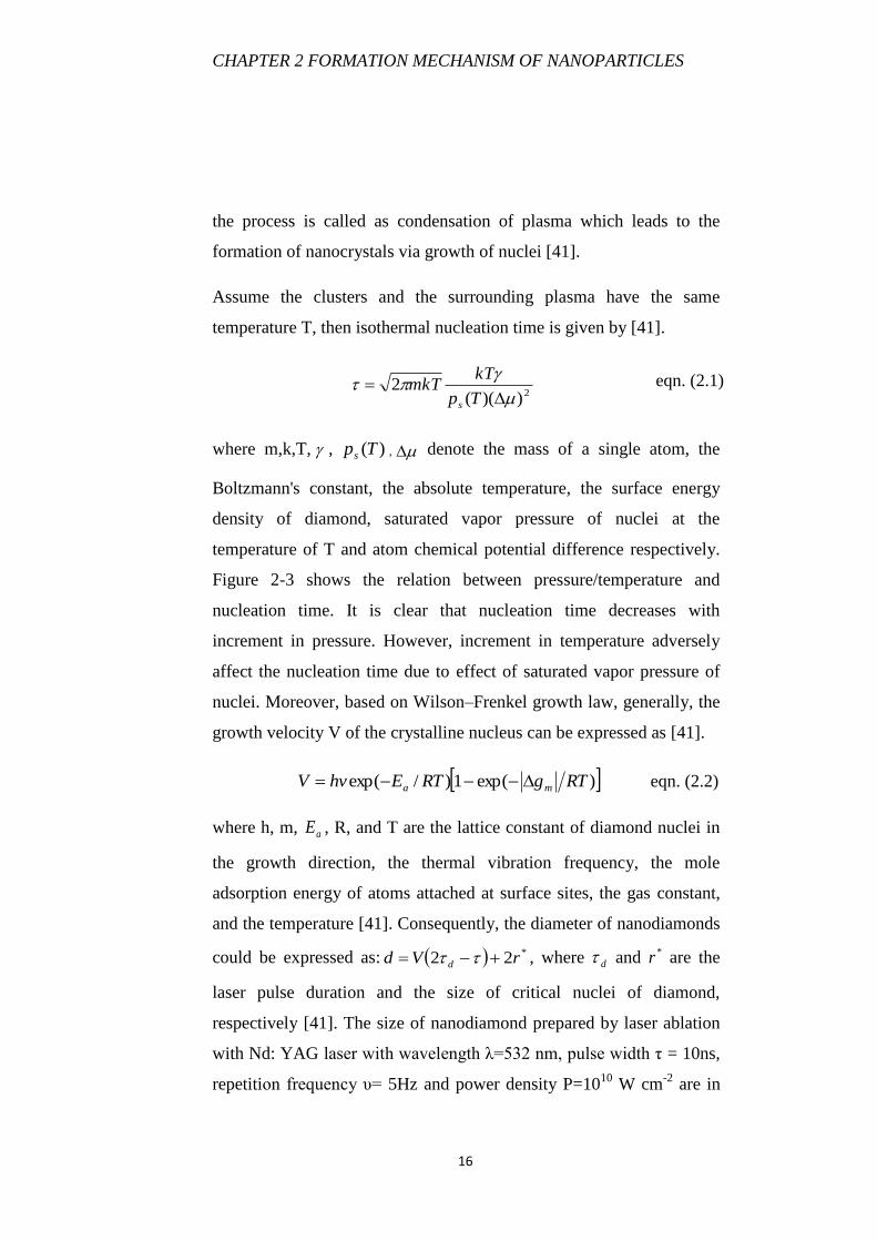
Figure 2-3 shows the relation between pressure/temperature and
nucleation time. It is clear that nucleation time decreases with
increment in pressure. However, increment in temperature adversely
affect the nucleation time due to effect of saturated vapor pressure of
nuclei. Moreover, based on Wilson–Frenkel growth law, generally, the
growth velocity V of the crystalline nucleus can be expressed as [41].
)exp(1)/exp( RTgRTEhvV ma eqn. (2.2)
where h, m, aE , R, and T are the lattice constant of diamond nuclei in
the growth direction, the thermal vibration frequency, the mole
adsorption energy of atoms attached at surface sites, the gas constant,
and the temperature [41]. Consequently, the diameter of nanodiamonds
could be expressed as: *22 rVd d , where d and *r are the
laser pulse duration and the size of critical nuclei of diamond,
respectively [41]. The size of nanodiamond prepared by laser ablation
with Nd: YAG laser with wavelength λ=532 nm, pulse width τ = 10ns,
repetition frequency υ= 5Hz and power density P=1010
W cm-2
are in
eqn. (2.1)
CHAPTER 2 FORMATION MECHANISM OF NANOPARTICLES
17
the range of 40 to 200 nm and this is perfectly fit with formula
*22 rVd d [45]. Therefore, these theoretical results are in well
agreement with experimental cases and can be employed to control the
size of nanocrystals synthesized by laser ablation in liquids [41].
Figure 2-3. The Relation between nucleation time and pressure.
Adopted from [41].
CHAPTER 3 EXPERIMENTAL RESULTS AND DISCUSSIONS
18
Chapter 3
3. Experimental Results and Discussions
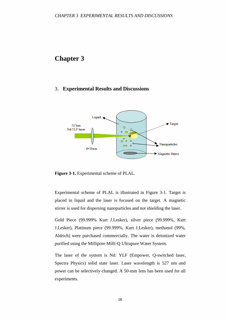
Figure 3-1. Experimental scheme of PLAL.
Experimental scheme of PLAL is illustrated in Figure 3-1. Target is
placed in liquid and the laser is focused on the target. A magnetic
stirrer is used for dispersing nanoparticles and not shielding the laser.
Gold Piece (99.999% Kurt J.Lesker), silver piece (99.999%, Kurt
J.Lesker), Platinum piece (99.999%, Kurt J.Lesker), methanol (99%,
Aldrich) were purchased commercially. The water is deionized water
purified using the Millipore Milli-Q Ultrapure Water System.
The laser of the system is Nd: YLF (Empower, Q-switched laser,
Spectra Physics) solid state laser. Laser wavelength is 527 nm and
power can be selectively changed. A 50-mm lens has been used for all
experiments.
CHAPTER 3 EXPERIMENTAL RESULTS AND DISCUSSIONS
19
First, Au, Ag and Pt NPs were synthesized in deionized water.
Secondly, these NPs were synthesized in methanol. Applications of
NMNPs, such as NMNP synthesization in polymeric solution for
nanofibers, effects of varying average powers, thin film deposition has
also been studied. Firstly, Au and Ag NPs were synthesized in
Polyvinylpyrolidone (PVP) for obtaining nanofibrous composites.
Secondly, AuNPs synthesized with varying average power of laser
were studied in order to understand the effect of average laser power
on NP synthesis. Lastly, thin film deposition of glass in liquid and
colloidal thin film application of NPs with spin coating was
investigated.
3.1 Gold, Silver and Platinum Nanoparticle Synthesis in
Water
Au, Ag and Pt NPs were synthesized in water by using pulsed Nd:YLF
laser (Empower, Q-Switched Laser, Spectra Physics, USA) with 527
nm wavelength, 16 W average power, 110 ns pulse duration, and 16 mJ
pulse energy for 1 kHz. The ablation was carried out for 5 min for each
synthesis. The laser was focused on the Au, Ag and Pt targets by a lens
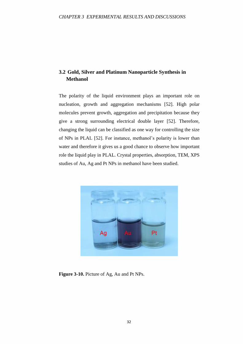
with focal length of 50 mm. The intensity of color of Ag, Au and Pt
NPs increased with irradiation time and the energy density of the laser
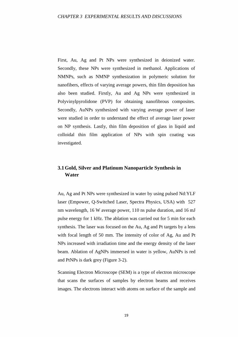
beam. Ablation of AgNPs immersed in water is yellow, AuNPs is red
and PtNPs is dark grey (Figure 3-2).
Scanning Electron Microscope (SEM) is a type of electron microscope
that scans the surfaces of samples by electron beams and receives
images. The electrons interact with atoms on surface of the sample and
CHAPTER 3 EXPERIMENTAL RESULTS AND DISCUSSIONS
20
produce signals which can be measured with special detectors inside
SEM. The types of signals that can be generated from the surface of the
samples are secondary electrons, back scattered electrons and
characteristic X-Rays.
Figure 3-2. Picture Ag, Au, and Pt NPs synthesized in water.
SEM gives detailed information about sample surface and topography,
chemical composition, electrical conductivity and image that optical
microscopes cannot resolve. FEI-Quanta 200 FEG model was used for
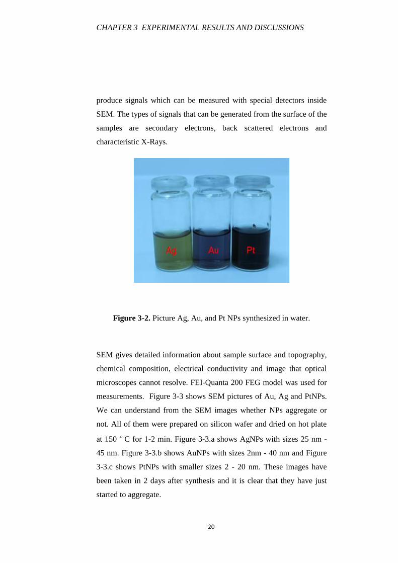
measurements. Figure 3-3 shows SEM pictures of Au, Ag and PtNPs.
We can understand from the SEM images whether NPs aggregate or
not. All of them were prepared on silicon wafer and dried on hot plate
at 150 C for 1-2 min. Figure 3-3.a shows AgNPs with sizes 25 nm -
45 nm. Figure 3-3.b shows AuNPs with sizes 2nm - 40 nm and Figure
3-3.c shows PtNPs with smaller sizes 2 - 20 nm. These images have
been taken in 2 days after synthesis and it is clear that they have just
started to aggregate.
CHAPTER 3 EXPERIMENTAL RESULTS AND DISCUSSIONS
21
Figure 3-3. SEM pictures of Au, Ag, PtNPs in Water a) AgNPs, b)
AuNPs, c) PtNPs.
a) b)
c)
CHAPTER 3 EXPERIMENTAL RESULTS AND DISCUSSIONS
22
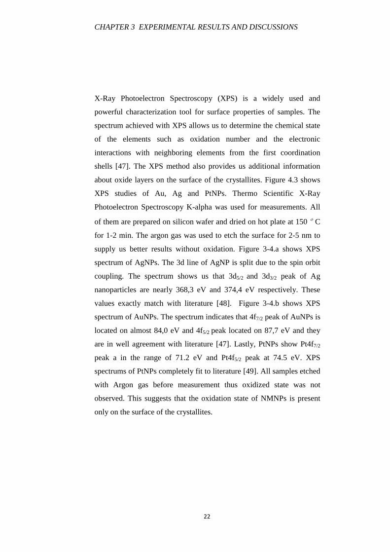
X-Ray Photoelectron Spectroscopy (XPS) is a widely used and
powerful characterization tool for surface properties of samples. The
spectrum achieved with XPS allows us to determine the chemical state
of the elements such as oxidation number and the electronic
interactions with neighboring elements from the first coordination
shells [47]. The XPS method also provides us additional information
about oxide layers on the surface of the crystallites. Figure 4.3 shows
XPS studies of Au, Ag and PtNPs. Thermo Scientific X-Ray
Photoelectron Spectroscopy K-alpha was used for measurements. All
of them are prepared on silicon wafer and dried on hot plate at 150 C
for 1-2 min. The argon gas was used to etch the surface for 2-5 nm to
supply us better results without oxidation. Figure 3-4.a shows XPS
spectrum of AgNPs. The 3d line of AgNP is split due to the spin orbit
coupling. The spectrum shows us that 3d5/2 and 3d3/2 peak of Ag
nanoparticles are nearly 368,3 eV and 374,4 eV respectively. These
values exactly match with literature [48]. Figure 3-4.b shows XPS
spectrum of AuNPs. The spectrum indicates that 4f7/2 peak of AuNPs is
located on almost 84,0 eV and 4f5/2 peak located on 87,7 eV and they
are in well agreement with literature [47]. Lastly, PtNPs show Pt4f7/2
peak a in the range of 71.2 eV and Pt4f5/2 peak at 74.5 eV. XPS
spectrums of PtNPs completely fit to literature [49]. All samples etched
with Argon gas before measurement thus oxidized state was not
observed. This suggests that the oxidation state of NMNPs is present
only on the surface of the crystallites.
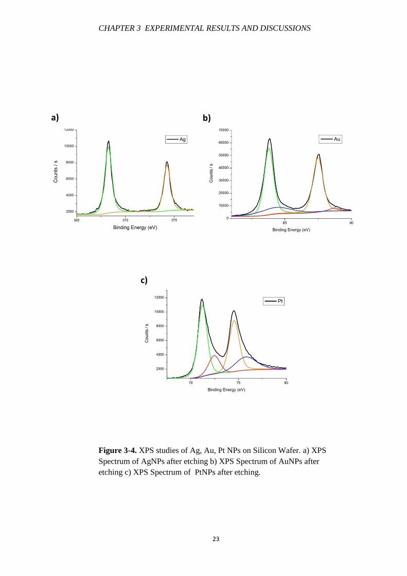
CHAPTER 3 EXPERIMENTAL RESULTS AND DISCUSSIONS
23
Figure 3-4. XPS studies of Ag, Au, Pt NPs on Silicon Wafer. a) XPS
Spectrum of AgNPs after etching b) XPS Spectrum of AuNPs after
etching c) XPS Spectrum of PtNPs after etching.
a) b)
c)
CHAPTER 3 EXPERIMENTAL RESULTS AND DISCUSSIONS
24
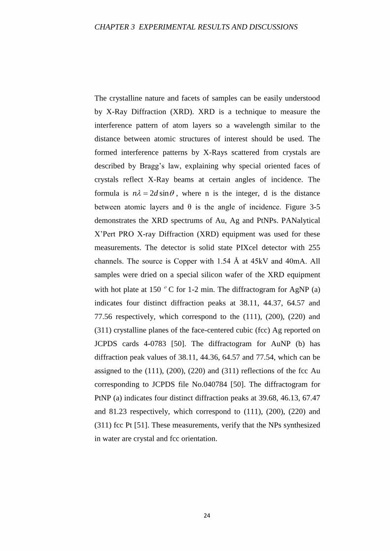
The crystalline nature and facets of samples can be easily understood
by X-Ray Diffraction (XRD). XRD is a technique to measure the
interference pattern of atom layers so a wavelength similar to the
distance between atomic structures of interest should be used. The
formed interference patterns by X-Rays scattered from crystals are
described by Bragg’s law, explaining why special oriented faces of
crystals reflect X-Ray beams at certain angles of incidence. The
formula is sin2dn , where n is the integer, d is the distance
between atomic layers and θ is the angle of incidence. Figure 3-5
demonstrates the XRD spectrums of Au, Ag and PtNPs. PANalytical
X’Pert PRO X-ray Diffraction (XRD) equipment was used for these
measurements. The detector is solid state PIXcel detector with 255
channels. The source is Copper with 1.54 Å at 45kV and 40mA. All
samples were dried on a special silicon wafer of the XRD equipment
with hot plate at 150 C for 1-2 min. The diffractogram for AgNP (a)
indicates four distinct diffraction peaks at 38.11, 44.37, 64.57 and
77.56 respectively, which correspond to the (111), (200), (220) and
(311) crystalline planes of the face-centered cubic (fcc) Ag reported on
JCPDS cards 4-0783 [50]. The diffractogram for AuNP (b) has
diffraction peak values of 38.11, 44.36, 64.57 and 77.54, which can be
assigned to the (111), (200), (220) and (311) reflections of the fcc Au
corresponding to JCPDS file No.040784 [50]. The diffractogram for
PtNP (a) indicates four distinct diffraction peaks at 39.68, 46.13, 67.47
and 81.23 respectively, which correspond to (111), (200), (220) and
(311) fcc Pt [51]. These measurements, verify that the NPs synthesized
in water are crystal and fcc orientation.
CHAPTER 3 EXPERIMENTAL RESULTS AND DISCUSSIONS
25
Figure 3-5. XRD studies of Ag, Au and Pt NPs. a) Ag NPs, b) Au
NPs, c) Pt NPs.
a)
c)
b)
CHAPTER 3 EXPERIMENTAL RESULTS AND DISCUSSIONS
26
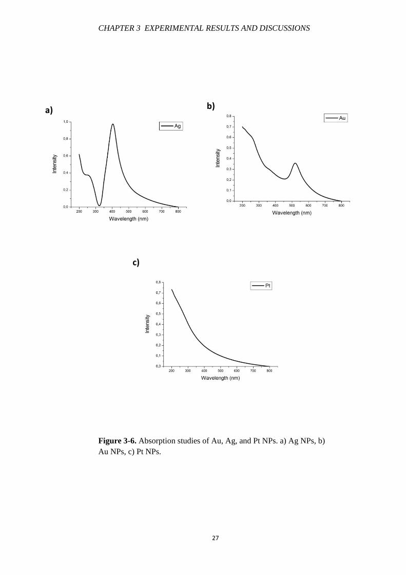
UV-Vis Spectroscopy or Absorption Spectroscopy is a spectroscopy
technique for absorption or reflectance measurements for solid and
liquid samples. Basically, the spectrophotometer sends white light to
the monochromator which transmits specific wavelengths. Then, the
selected wavelength of light reaches the sample and spectrophotometer
behind sample detects remaining photons by its detector. Figure 3-6
specifies absorption studies of Ag, Au and Pt NPs. The absorption
spectrum of the solution has been measured by Cary 5000 UV-Vis-NIR
Spectrophotometer. Baseline correction and double beam mode are
used. The average time between two single measurements for single
wavelength is 0.100 sec. There are little effects of source change at 350
nm. The data has been taken from 200 nm to 800 nm. All
measurements had been performed in 2 days after synthesization. The
AgNP spectrum exhibits a characteristic peak at 402 nm, the well-
known surface plasmon resonance of spherical particles for AgNP [52].
AuNP has peak at 520 nm. The 520 nm peak of Au NPs is well-known.
It shows that AuNPs has elongated shape [53]. The PtNP spectrum
exhibits a broad band extending UV range and this is well agreement
with literature [54].
CHAPTER 3 EXPERIMENTAL RESULTS AND DISCUSSIONS
27
Figure 3-6. Absorption studies of Au, Ag, and Pt NPs. a) Ag NPs, b)
Au NPs, c) Pt NPs.
a) b)
c)
CHAPTER 3 EXPERIMENTAL RESULTS AND DISCUSSIONS
28
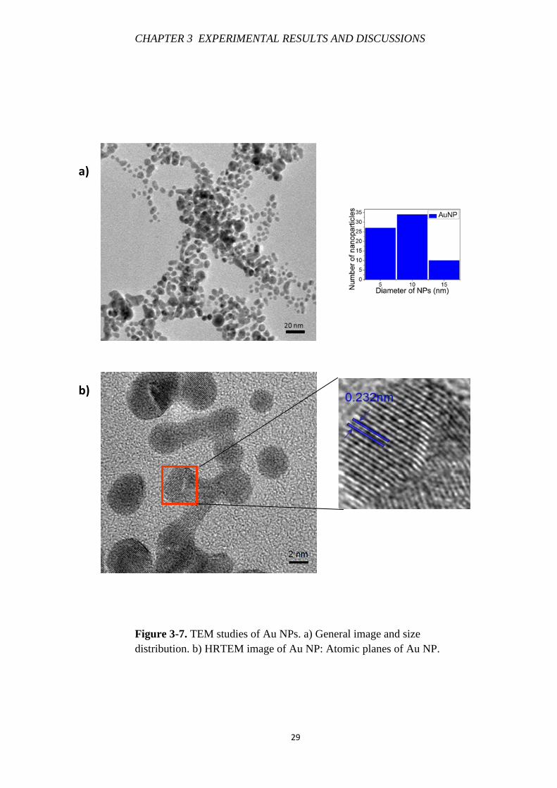
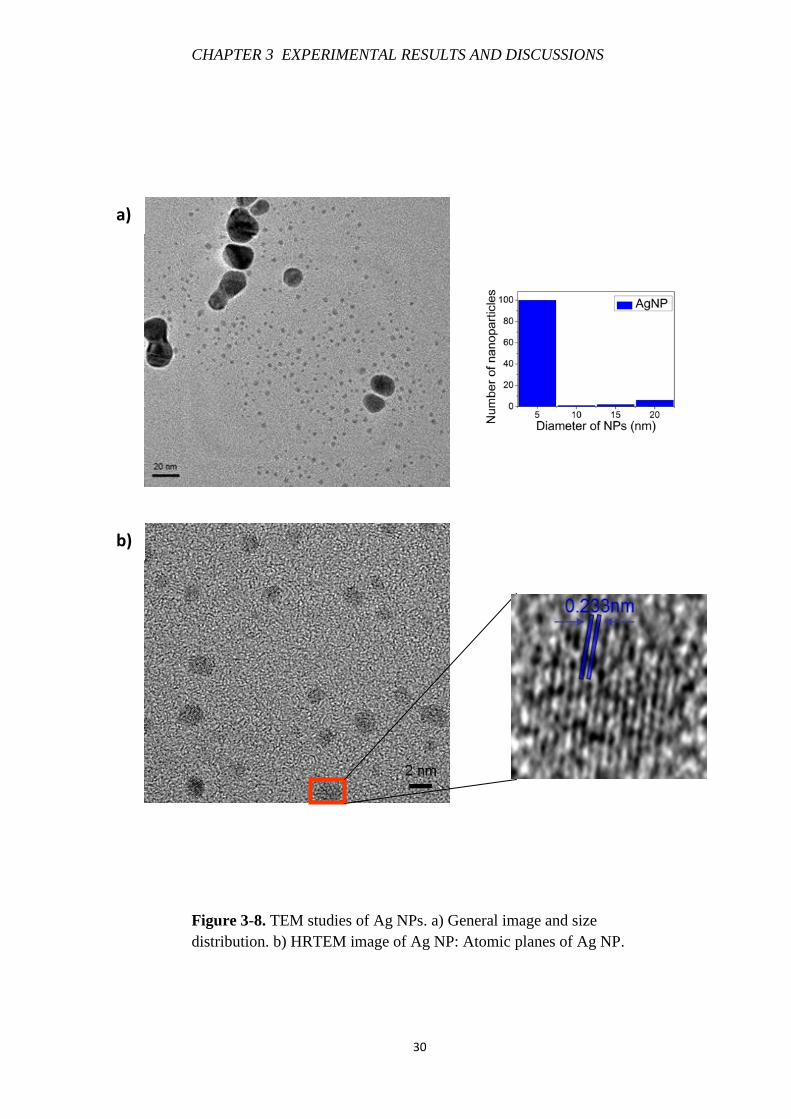
Transmission Electron Microscope (TEM) is basically a type of
electron microscope that sends electron beams to the sample and
detects it with CCD detectors. Thank to de Broglie wavelength of
electrons, it supplies super resolution, even one can detect a column of
atoms. It plays a significant role for detecting NPs. One can measure
size distribution of NPs, gather information about whether they are
crystal. FEI Technai G2 F30 TEM was used for the measurements. All
samples were prepared immediately after laser ablation synthesis. Size
distributions of particles were carried out by calculation over 200
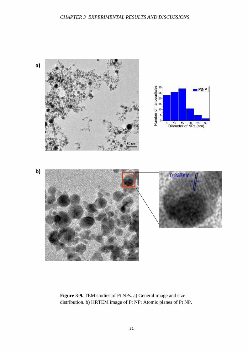
nanoparticles. Figure 3-7.a shows TEM image of AuNP. AuNP size
distribution changes from 2.5nm to 25 nm. The HRTEM images (see
Figure 4-7.b) of AuNP clearly state that lattice fringe separation is
0.232 nm [55]. This separation indicates that AuNP has (111)
orientation. Ag NP sizes vary from 2.5 to 20 nm. Indeed, they are
mostly in the range of 1-7.5 nm. Much bigger nanoparticles also were
detected as seen in Figure 3-8.a. The lattice fringe separation is 0.233
nm. This value shows that AgNP has (111) orientation [56]. PtNP sizes
are in the range of 1-32 nm and mostly are smaller than 20nm. The
lattice fringe separation of PtNP is 0.237nm. This separation indicates
that PtNP has (111) orientation [57].
CHAPTER 3 EXPERIMENTAL RESULTS AND DISCUSSIONS
29
Figure 3-7. TEM studies of Au NPs. a) General image and size
distribution. b) HRTEM image of Au NP: Atomic planes of Au NP.
a)
b)
CHAPTER 3 EXPERIMENTAL RESULTS AND DISCUSSIONS
30
Figure 3-8. TEM studies of Ag NPs. a) General image and size
distribution. b) HRTEM image of Ag NP: Atomic planes of Ag NP.
a)
b)
CHAPTER 3 EXPERIMENTAL RESULTS AND DISCUSSIONS
31
Figure 3-9. TEM studies of Pt NPs. a) General image and size
distribution. b) HRTEM image of Pt NP: Atomic planes of Pt NP.
a)
b)
CHAPTER 3 EXPERIMENTAL RESULTS AND DISCUSSIONS
32
3.2 Gold, Silver and Platinum Nanoparticle Synthesis in
Methanol
The polarity of the liquid environment plays an important role on
nucleation, growth and aggregation mechanisms [52]. High polar
molecules prevent growth, aggregation and precipitation because they
give a strong surrounding electrical double layer [52]. Therefore,
changing the liquid can be classified as one way for controlling the size
of NPs in PLAL [52]. For instance, methanol’s polarity is lower than
water and therefore it gives us a good chance to observe how important
role the liquid play in PLAL. Crystal properties, absorption, TEM, XPS
studies of Au, Ag and Pt NPs in methanol have been studied.
Figure 3-10. Picture of Ag, Au and Pt NPs.
CHAPTER 3 EXPERIMENTAL RESULTS AND DISCUSSIONS
33
Au, Ag and Pt NPs were synthesized in methanol by using pulsed Nd:
YLF laser (Empower, Q-Switched Laser, Spectra Physics, USA) with
527 nm wavelength, 16 W average power, 110 ns pulse duration, and
16 mJ pulse energy for 1 kHz. The ablation was carried out for 5-10
min for each synthesis.
In methanol, since the polarity is decreased with regard to water,
precipitation occurs in two or three days. Therefore, all measurements
and preparation of samples have been performed immediately after
laser ablation synthesis of Ag, Au and Pt NPs in liquid achieved.
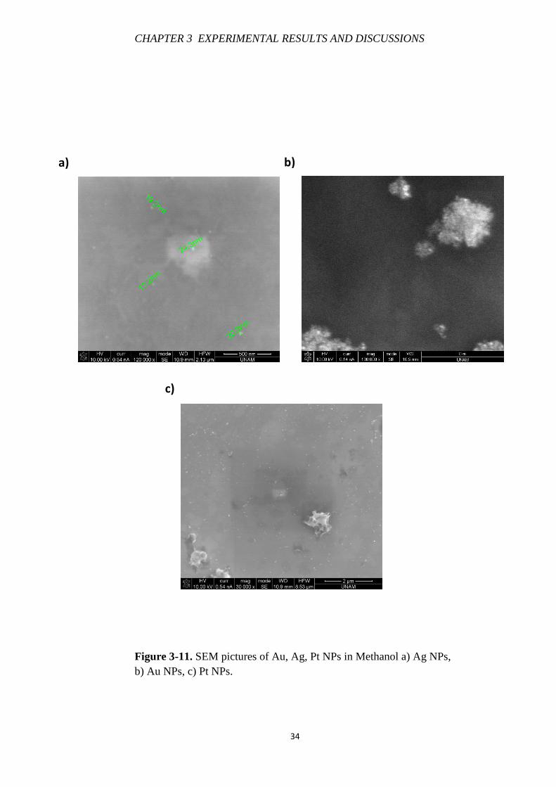
SEM images of Au, Ag and Pt NPs are not so clear but they give
estimation about the sizes of nanoparticles and how they spread. All of
the samples are prepared on silicon wafer and dried on hot plate at 100
C for 1-2 min. The samples of Au, Ag, and Pt NPs for SEM were
taken immediately after laser ablation synthesis. SEM images show
that AgNPs sizes are 19-25 nm and they are dispersed. Some
aggregations were also observed. AuNPs sizes are small and united.
PtNPs are well dispersed and there is no aggregation.
CHAPTER 3 EXPERIMENTAL RESULTS AND DISCUSSIONS
34
Figure 3-11. SEM pictures of Au, Ag, Pt NPs in Methanol a) Ag NPs,
b) Au NPs, c) Pt NPs.
c)
a) b)
CHAPTER 3 EXPERIMENTAL RESULTS AND DISCUSSIONS
35
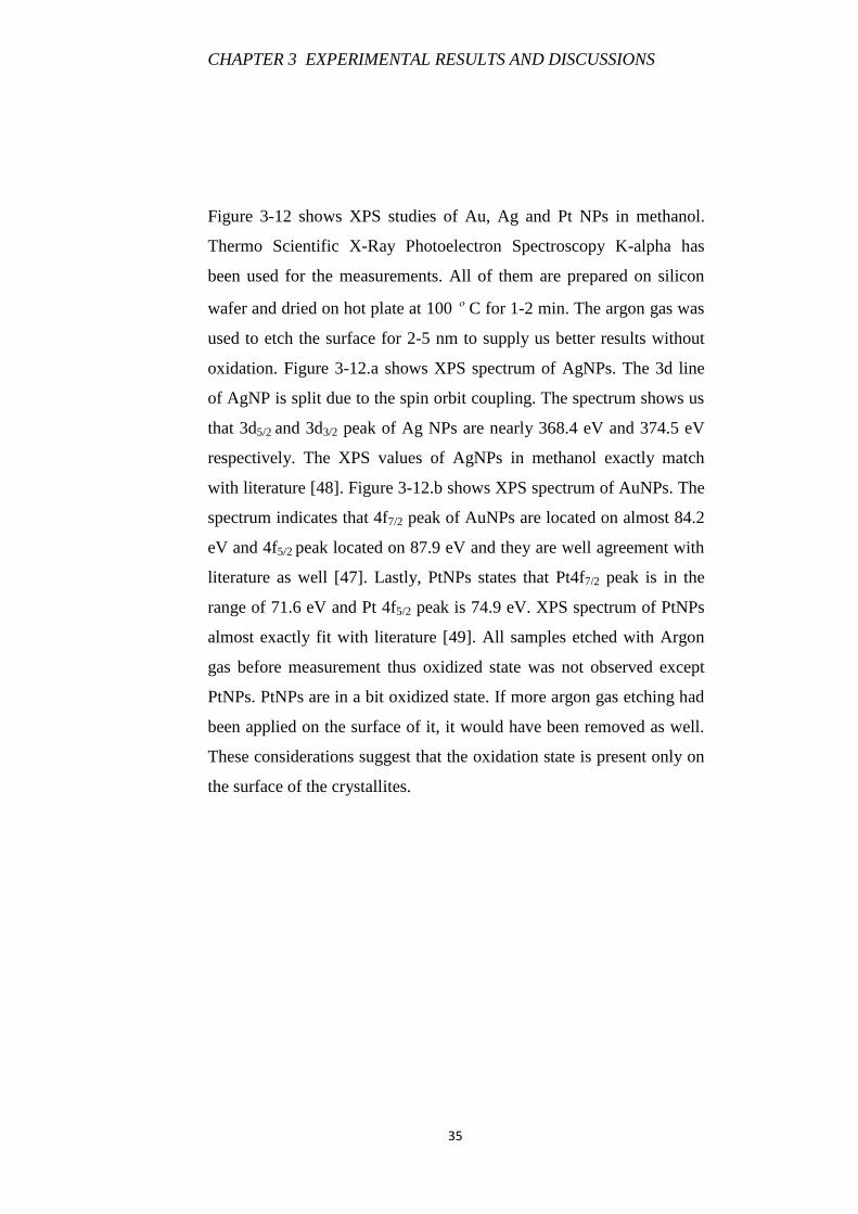
Figure 3-12 shows XPS studies of Au, Ag and Pt NPs in methanol.
Thermo Scientific X-Ray Photoelectron Spectroscopy K-alpha has
been used for the measurements. All of them are prepared on silicon
wafer and dried on hot plate at 100 C for 1-2 min. The argon gas was
used to etch the surface for 2-5 nm to supply us better results without
oxidation. Figure 3-12.a shows XPS spectrum of AgNPs. The 3d line
of AgNP is split due to the spin orbit coupling. The spectrum shows us
that 3d5/2 and 3d3/2 peak of Ag NPs are nearly 368.4 eV and 374.5 eV
respectively. The XPS values of AgNPs in methanol exactly match
with literature [48]. Figure 3-12.b shows XPS spectrum of AuNPs. The
spectrum indicates that 4f7/2 peak of AuNPs are located on almost 84.2
eV and 4f5/2 peak located on 87.9 eV and they are well agreement with
literature as well [47]. Lastly, PtNPs states that Pt4f7/2 peak is in the
range of 71.6 eV and Pt 4f5/2 peak is 74.9 eV. XPS spectrum of PtNPs
almost exactly fit with literature [49]. All samples etched with Argon
gas before measurement thus oxidized state was not observed except
PtNPs. PtNPs are in a bit oxidized state. If more argon gas etching had
been applied on the surface of it, it would have been removed as well.
These considerations suggest that the oxidation state is present only on
the surface of the crystallites.
CHAPTER 3 EXPERIMENTAL RESULTS AND DISCUSSIONS
36
Figure 3-12. XPS studies of Au, Ag, Pt NPs in Methanol a) Ag NPs, b)
Au NPs, c) Pt NPs.
c)
b) a)
CHAPTER 3 EXPERIMENTAL RESULTS AND DISCUSSIONS
37
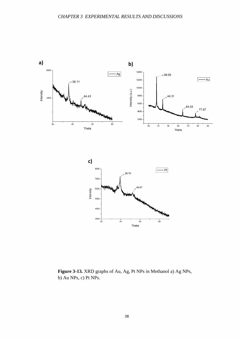
Figure 3-13 demonstrates the XRD spectrums of Au, Ag and PtNPs in
methanol. PANalytical X’Pert PRO X-ray Diffraction equipment was
used for these measurements. All samples were dried on a special
silicon wafer of the equipment with hot plate at 90 C for 1-2 min. The
diffractogram for AgNP indicates two distinct diffraction peaks at
38.11, 44.43 which correspond to the (111), (200) crystalline planes of
the Ag reported on JCPDS cards 4-0783 [50]. The diffractogram for
AuNP has diffraction peak values of 38.09, 44.31, 64.53 and 77.67,
which can be assigned to the (111), (200), (220) and (311) reflections
of the fcc Au corresponding to JCPDS file No.040784 [50]. The
diffractogram for PtNP (a) indicates two distinct diffraction peaks at
39.70, 46.07 respectively, which correspond to (111) and (200)
crystalline planes of the Pt. These measurements verify that the
NMNPs synthesized in methanol are crystal. However, it was
surprising that (220) and (311) crystal planes of Ag and PtNPs were
not observed.
CHAPTER 3 EXPERIMENTAL RESULTS AND DISCUSSIONS
38
Figure 3-13. XRD graphs of Au, Ag, Pt NPs in Methanol a) Ag NPs,
b) Au NPs, c) Pt NPs.
a) b)
c)
CHAPTER 3 EXPERIMENTAL RESULTS AND DISCUSSIONS
39
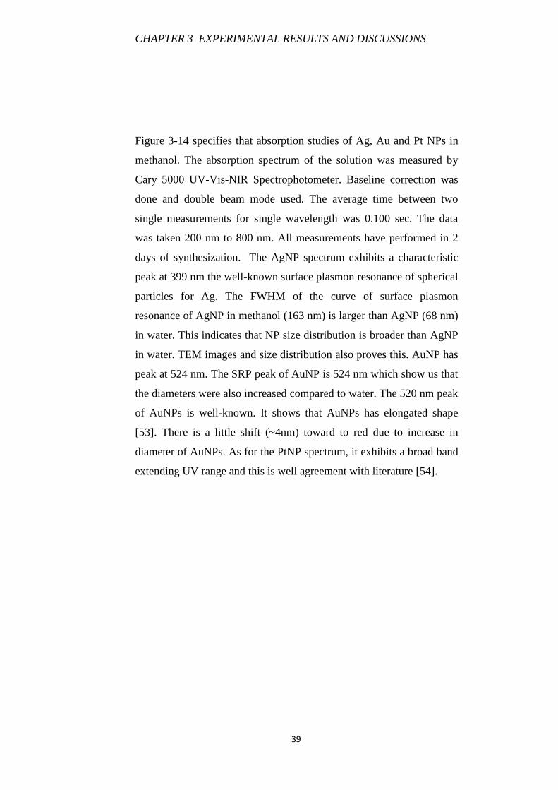
Figure 3-14 specifies that absorption studies of Ag, Au and Pt NPs in
methanol. The absorption spectrum of the solution was measured by
Cary 5000 UV-Vis-NIR Spectrophotometer. Baseline correction was
done and double beam mode used. The average time between two
single measurements for single wavelength was 0.100 sec. The data
was taken 200 nm to 800 nm. All measurements have performed in 2
days of synthesization. The AgNP spectrum exhibits a characteristic
peak at 399 nm the well-known surface plasmon resonance of spherical
particles for Ag. The FWHM of the curve of surface plasmon
resonance of AgNP in methanol (163 nm) is larger than AgNP (68 nm)
in water. This indicates that NP size distribution is broader than AgNP
in water. TEM images and size distribution also proves this. AuNP has
peak at 524 nm. The SRP peak of AuNP is 524 nm which show us that
the diameters were also increased compared to water. The 520 nm peak
of AuNPs is well-known. It shows that AuNPs has elongated shape
[53]. There is a little shift (~4nm) toward to red due to increase in
diameter of AuNPs. As for the PtNP spectrum, it exhibits a broad band
extending UV range and this is well agreement with literature [54].
CHAPTER 3 EXPERIMENTAL RESULTS AND DISCUSSIONS
40
Figure 3-14. Absorption studies of Au, Ag, and Pt NPs. a) Ag NPs, b)
Au NPs, c) Pt NPs.
a) b)
c)
CHAPTER 3 EXPERIMENTAL RESULTS AND DISCUSSIONS
41
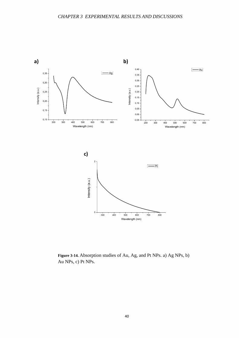
FEI Technai G2 F30 TEM was used for the measurements. All samples
were prepared immediately after laser ablation synthesis. Size
distributions of NPs were done by calculation over 200 nanoparticles.
Figure 3-15 shows TEM image of AuNP in methanol. AuNP size
distribution changes from 2.5 nm to 20 nm. The TEM images of AuNP
clearly state that lattice fringe separation is 2.32 A° [55]. This
separation indicates that AuNP has (111) orientation. AgNP sizes vary
from 2.5 to 20 nm. However, they are mostly in the range of 1-7.5 nm.
Much bigger nanoparticles also were detected as seen in Figure 3-16.
AgNPs lattice fringe 2.29 A° corresponds to (111) orientation [56].
PtNP sizes are in the range of 1-32 nm and mostly are smaller than
20nm. HRTEM image of PtNPs shows that the crystalline structures
can be identified by their typical lattice fringes (see Figure 3-17). A
large number of the particles can be viewed with clear (111) lattice
fringes with a lattice spacing of 2.35 A° [57].
CHAPTER 3 EXPERIMENTAL RESULTS AND DISCUSSIONS
42
Figure 3-15. TEM studies of Au NPs in methanol. a) General image
and size distribution. b) HRTEM image of Au NP: Atomic planes of
Au NP.
a)
b)
CHAPTER 3 EXPERIMENTAL RESULTS AND DISCUSSIONS
43
Figure 3-16. TEM studies of Ag nanoparticles in methanol. a) General
image and size distribution. b) HRTEM image of Ag NP: Atomic
planes of Ag NP.
b)
a)
CHAPTER 3 EXPERIMENTAL RESULTS AND DISCUSSIONS
44
Figure 3-17. TEM studies of Pt nanoparticles in methanol. a) General
image and size distribution. b) HRTEM image of Pt NP: Atomic planes
of Pt NP.
a)
b)
CHAPTER 3 EXPERIMENTAL RESULTS AND DISCUSSIONS
45
3.3 Gold and Silver Nanoparticles Synthesis in Polymeric
Solution
AuNPs and AgNPs were synthesized in PVP by using pulsed Nd: YLF
laser (Empower, Q-Switched Laser, Spectra Physics, USA) with 527
nm wavelength, 16 W average power, 110 ns pulse duration, and 16 mJ
pulse energy for 1 kHz. The ablation was carried out for 15 min for
synthesis.
PVP is a water soluble polymer having a hydrophilic nature and it is
widely used as a stabilizer and capping agent for AuNPs and AgNPs.
Therefore, PVP can protect the NPs from agglomeration in the medium
[10].
After AuNPs and AgNPs are prepared in PVP, the electrospinning of
PVP/AuNPs and AgNPs solution was carried out for obtaining
nanofibrous composites by Uyar Research Group at UNAM, Bilkent
University.
UV-Vis-NIR Spectrophotometer and TEM studies were done from Au
and Ag NPs embedded in nanofibers. FEI Technai G2 F30 TEM was
used for the measurements. The AuNPs were in spherical form having
average diameter in the range of 5 to 20 nm. They were mostly
dispersed homogeneously in the PVP matrix, however, some
aggregations of the AuNPs were also observed (Please see Figure
3-18.b). As for Ag NPs, their sizes change from 5 to 25 nm.
Aggregations of Ag NPs were also observed. The dispersion of AgNPs
on the surface of nanofibers is not as successful as AuNPs dispersion.
(Please see Figure 3-18.b.)
CHAPTER 3 EXPERIMENTAL RESULTS AND DISCUSSIONS
46
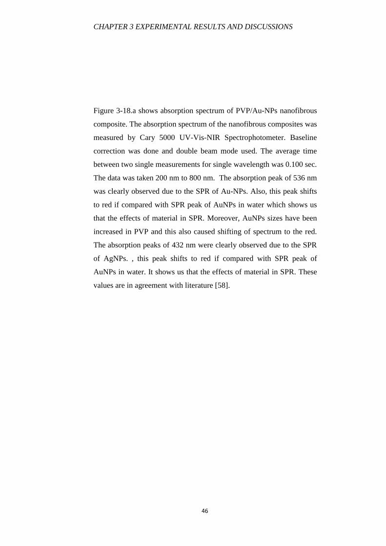
Figure 3-18.a shows absorption spectrum of PVP/Au-NPs nanofibrous
composite. The absorption spectrum of the nanofibrous composites was
measured by Cary 5000 UV-Vis-NIR Spectrophotometer. Baseline
correction was done and double beam mode used. The average time
between two single measurements for single wavelength was 0.100 sec.
The data was taken 200 nm to 800 nm. The absorption peak of 536 nm
was clearly observed due to the SPR of Au-NPs. Also, this peak shifts
to red if compared with SPR peak of AuNPs in water which shows us
that the effects of material in SPR. Moreover, AuNPs sizes have been
increased in PVP and this also caused shifting of spectrum to the red.
The absorption peaks of 432 nm were clearly observed due to the SPR
of AgNPs. , this peak shifts to red if compared with SPR peak of
AuNPs in water. It shows us that the effects of material in SPR. These
values are in agreement with literature [58].
CHAPTER 3 EXPERIMENTAL RESULTS AND DISCUSSIONS
47
Figure 3-18. Absorption and TEM studies of Au and AgNPs
embedded in nanofibers [10]. The Au-NPs were directly synthesized in
PVP solution by laser ablation and then, the electrospinning of
PVP/Au-NPs solution was carried out for obtaining nanofibrous
composites [10]. a) Absorption study of of Au and AgNPs embedded
nanofibers. b) TEM studies of of Ag and AuNPs embedded nanofibers.
AgNPs AuNPs b)
a)
CHAPTER 3 EXPERIMENTAL RESULTS AND DISCUSSIONS
48
3.4 Gold Nanoparticle Synthesis in Water with Different
Average Powers
AuNPs were synthesized with Nd: YLF laser with different average
power of the laser. If one of the main parameters of laser ablation, such
as energy, wavelength and solvent changes, NP sizes and shapes may
change. In order to control this dependency, AuNPs were synthesized
with different average powers.
Figure 3-19. Image of AuNPs in water synthesize in different average
powers.
Figure 3-20 demonstrates the absorption study of AuNP synthesized in
different average powers. The laser is Nd: YLF laser (Empower, Q-
Switched Laser, Spectra Physics, USA) with 527 nm wavelength. Red
line indicates AuNPs synthesized in deionized water with the condition
of 9.2 W average power, 150 ns pulse duration, and 9.2 mJ pulse
CHAPTER 3 EXPERIMENTAL RESULTS AND DISCUSSIONS
49
energy for 1 kHz for Nd: YLF laser. Green line represents the laser
parameters as 12 W average power, 130 ns pulse duration, and 12 mJ
pulse energy for 1 kHz. Blue line corresponds to 16 W average power,
110 ns pulse duration and 16 mJ pulse energy for 1 kHz laser
parameters.
Figure 3-20. Absorption study of AuNP synthesized in different
average powers. Blue line 16W, green line 12W and red line indicates
9.2W average powers. Their peak values change. Blue line has peak at
520nm, green line 518nm and red line 516nm peak values.
Absorption study of AuNP synthesized in different average powers
specifies that there occurs shift toward to red if average power of laser
is increased. Red line has peak value at 516 nm, green line has 518 nm
and blue line has at 520 nm. This shift arises from size of
nanoparticles. Each has different NP sizes and this causes the shift in
surface plasmon resonances. TEM gives clear results about the sizes
for 9.2W, 12W and 16W average power generation of AuNPs.
CHAPTER 3 EXPERIMENTAL RESULTS AND DISCUSSIONS
50
Each size distribution was obtained by measuring the diameters of
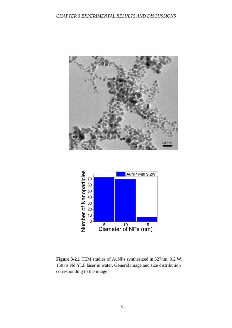
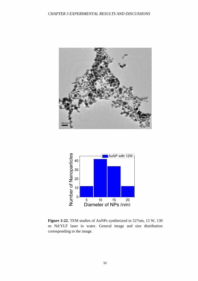
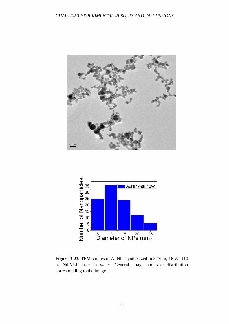
more than 150 particles in sight on the given micrograph. Figure 3-21
shows the AuNP synthesized in water by using pulsed 9.2 W average
power, 150 ns pulse duration, and 9.2 mJ pulse energy for 1 kHz. The
ablation was carried out for 10 min. Size distribution changes from
2.5nm to 17.5 nm and most of NPs are smaller than 12.5nm. Figure
3-22 shows the AuNP synthesized in water by using 12 W average
power, 130 ns pulse duration, and 12 mJ pulse energy for 1 kHz. The
ablation was carried out for 7 min. Size distribution changes from 2.5
nm to 22.5 nm and most of NPs are in the range of 7.5 nm to 17.5 nm.
Figure 3-23 shows the AuNP synthesized in water by 16 W average
power, 110 ns pulse duration, and 16 mJ pulse energy for 1 kHz. The
ablation was carried out for 5 min. The broadest distribution obtained
with these parameters. Nanoparticles change from 1 nm to 30 nm. As
expected from SPR measurement of AuNPs, the size distribution gets
larger if more average power is applied.
CHAPTER 3 EXPERIMENTAL RESULTS AND DISCUSSIONS
51
Figure 3-21. TEM studies of AuNPs synthesized in 527nm, 9.2 W,
150 ns Nd:YLF laser in water. General image and size distribution
corresponding to the image.
CHAPTER 3 EXPERIMENTAL RESULTS AND DISCUSSIONS
52
Figure 3-22. TEM studies of AuNPs synthesized in 527nm, 12 W, 130
ns Nd:YLF laser in water. General image and size distribution
corresponding to the image.
CHAPTER 3 EXPERIMENTAL RESULTS AND DISCUSSIONS
53
Figure 3-23. TEM studies of AuNPs synthesized in 527nm, 16 W, 110
ns Nd:YLF laser in water. General image and size distribution
corresponding to the image.
CHAPTER 3 EXPERIMENTAL RESULTS AND DISCUSSIONS
54
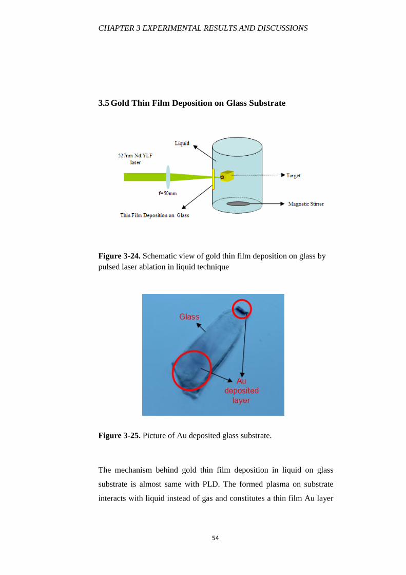
3.5 Gold Thin Film Deposition on Glass Substrate
Figure 3-24. Schematic view of gold thin film deposition on glass by
pulsed laser ablation in liquid technique
Figure 3-25. Picture of Au deposited glass substrate.
The mechanism behind gold thin film deposition in liquid on glass
substrate is almost same with PLD. The formed plasma on substrate
interacts with liquid instead of gas and constitutes a thin film Au layer
CHAPTER 3 EXPERIMENTAL RESULTS AND DISCUSSIONS
55
on the front face of the tube. The deposition of Au layer on glass has
been carried out by Nd: YLF laser (Empower, Q-Switched Laser,
Spectra Physics, USA) with 527 nm wavelength, 16 W average power,
110 ns pulse duration, and 16 mJ pulse energy for 1 kHz. Figure 3-24
indicates the schematic view of Au thin film deposition technique.
Figure 3-25 shows the pictures of Au deposited on glass substrate.
Figure 3-26. SEM and Optical pictures of Au deposited glass
substrates.
Au
SiO2 SiO2 Au Au
Au
CHAPTER 3 EXPERIMENTAL RESULTS AND DISCUSSIONS
56
Figure 3-26 shows SEM and optical pictures of Au deposited film.
One of the disadvantages of this process is obvious. The layer is not
homogenous and this technique cannot be applied on the fields where
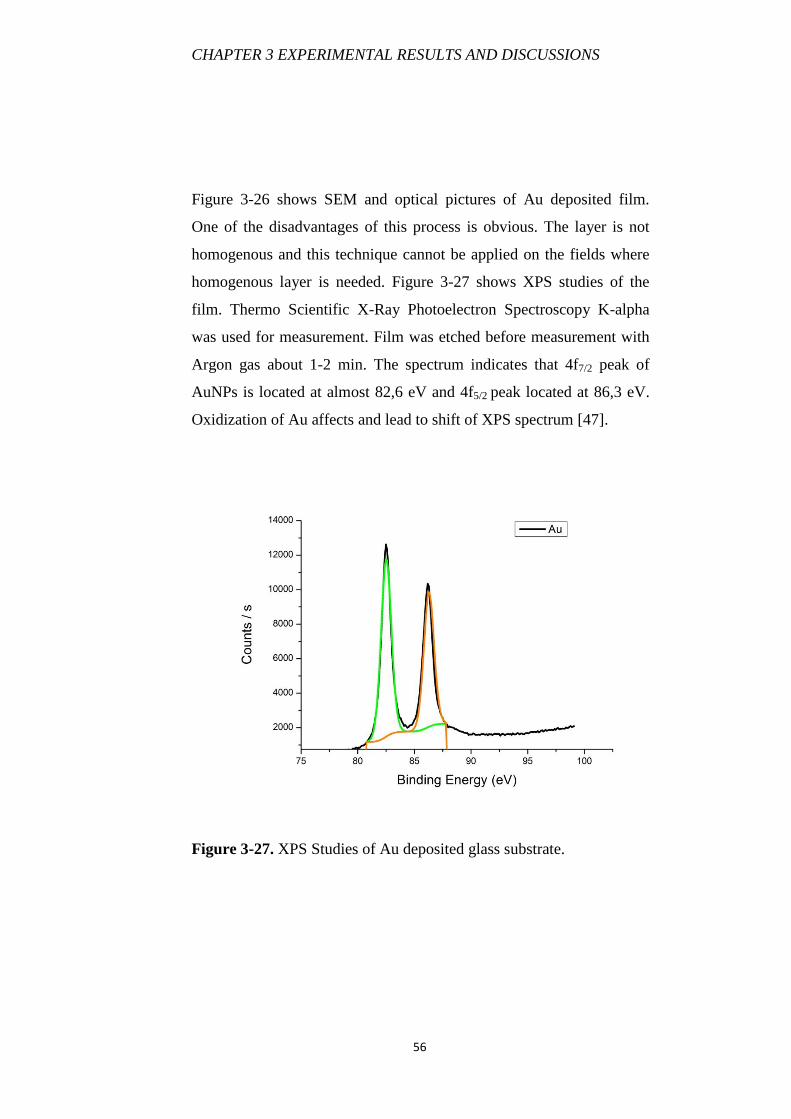
homogenous layer is needed. Figure 3-27 shows XPS studies of the
film. Thermo Scientific X-Ray Photoelectron Spectroscopy K-alpha
was used for measurement. Film was etched before measurement with
Argon gas about 1-2 min. The spectrum indicates that 4f7/2 peak of
AuNPs is located at almost 82,6 eV and 4f5/2 peak located at 86,3 eV.
Oxidization of Au affects and lead to shift of XPS spectrum [47].
Figure 3-27. XPS Studies of Au deposited glass substrate.
CHAPTER 3 EXPERIMENTAL RESULTS AND DISCUSSIONS
57
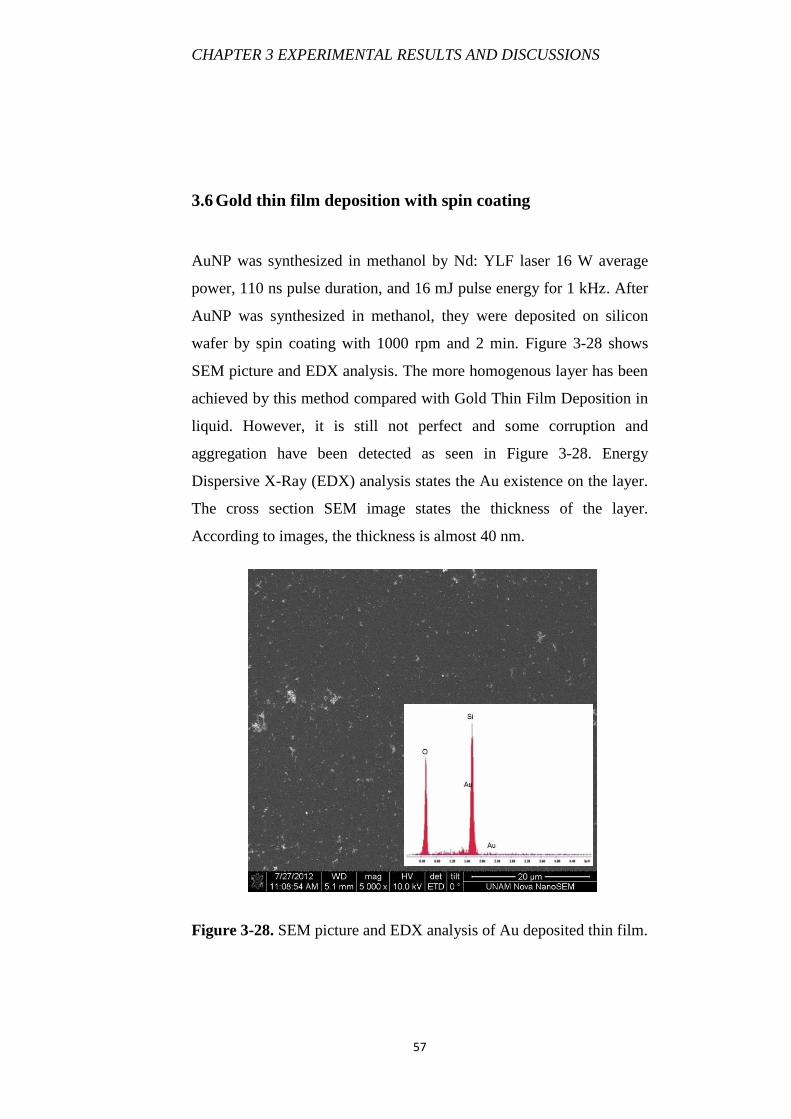
3.6 Gold thin film deposition with spin coating
AuNP was synthesized in methanol by Nd: YLF laser 16 W average
power, 110 ns pulse duration, and 16 mJ pulse energy for 1 kHz. After
AuNP was synthesized in methanol, they were deposited on silicon
wafer by spin coating with 1000 rpm and 2 min. Figure 3-28 shows
SEM picture and EDX analysis. The more homogenous layer has been
achieved by this method compared with Gold Thin Film Deposition in
liquid. However, it is still not perfect and some corruption and
aggregation have been detected as seen in Figure 3-28. Energy
Dispersive X-Ray (EDX) analysis states the Au existence on the layer.
The cross section SEM image states the thickness of the layer.
According to images, the thickness is almost 40 nm.
Figure 3-28. SEM picture and EDX analysis of Au deposited thin film.
CHAPTER 4 CONCLUSION & FUTURE WORK
58
Chapter 4
4. Conclusion
PLAL is a new and promising nanoparticle synthesization technique. It
is also free of chemical agents, ligands or stabilizers and relatively
cheap. It allows user to synthesize numerous type of nanoparticles from
semiconductors to magnetic materials only by a one process. Different
solvents or average power / pulse duration of laser change all
mechanism and lead to different sizes/shapes/crystallites of same
material. The synthesized nanoparticles with PLAL are mostly crystal
and the size distributions are not large. Therefore, they are good
candidates for many technological applications. An extensive work of
NMNp synthesization by PLAL has been presented. Beside theoretical
work of how nuclei and nanoparticles form with plasma, experimental
results were discussed in detail.
Firstly, Au, Ag and Pt NPs were synthesized in deionized water with
Nd: YLF laser (Q-Switched Laser, 527 nm wavelength, 16 W average
power, 110 ns pulse duration, and 16 mJ pulse energy for 1 kHz). They
were characterized with SEM, XPS, XRD, TEM, and UV-Vis
Spectroscopy. In addition, AuNPs in deionized water have been
synthesized with varying energies of laser (9,2 mJ, 12 mJ and 16 mJ
for 1kHz) in order to understand the role of laser energy on PLAL.
Secondly, these noble metals were synthesized in methanol with Nd:
YLF laser (Q-Switched Laser, 527 nm wavelength, 16 W average
power, 110 ns pulse duration, and 16 mJ pulse energy for 1 kHz).
CHAPTER 4 CONCLUSION & FUTURE WORK
59
Then, they were characterized with SEM, XPS, XRD, TEM, and UV-
Vis Spectroscopy. NPs obtained in deionized water are more stable
than in methanol. Also, small change in SPR and sizes of Ag, Au and
Pt NPs in deionized water and methanol was observed. These
differences were characterized with UV-Vis Spectroscopy and TEM.
Crystal properties and chemical compositions of NMNPs in deionized
water and methanol were same. Lastly, Au and Ag NPs were
synthesized in PVP for nanofibrous composites. The characterization
of Au and AgNPs in PVP was investigated by means of TEM and UV-
Vis Spectroscopy. Thin-film applications were also presented: PLD-
like deposition by PLAL and simple spin-coating deposition with
AuNPs synthesized in methanol. The films were not homogenous.
However, these two techniques of thin film deposition are an
alternative, easy and cheap method.
For future work, PLAL of different materials can be performed such as
semiconductors and metals. Also, NPs obtained by different lasers and
different wavelength liquid environments can be studied. Moreover,
synthesized NPs with PLAL can be investigated in applications,
namely, solar cell, optical sensors, and cancer treatment.
CHAPTER 5 BIBLIOGRAPHY
60
Bibliography
[1] S., Milunovic and M.A.J.Roy, "An Introduction to
Nanotechnology: The Next Small Thing," Merrill Lynch, 2001.
[2] R.P. Feynman, "There's Plenty of Room at the Bottom," Caltech's
Engineering and Science, 1960.
[3] A.K., Ali, "Preparation of Ag and Au Nanoparticles by Pulsed
Laser Ablation in Liquids," Baghdad University : PhD Thesis, 2010.
[4] S.Nie and S.R.Emory, "Probing Single Molecules and Single
Nanoparticles by Surface-Enhanced Raman Scattering," Science, vol.
275, p. 1102, 1997.
[5] Y., Cui, et al., "Integration of Colloidal Nanocrystals into
Lithographically Patterned Devices," Nano Letters,vol. 4, pp. 1093-
1098, 2004.
[6] R.Singh and J.W.Lillard, "Nanoparticle-based targeted drug
delivery," Experimental and Molecular Pathology, vol. 86, pp. 215-
223, 2009.
[7] K.Nakayama, K.Tanabe and H.A.Atwater, "Plasmonic
Nanoparticle Enhanced Light Absorbtion in GaAs Solar Cells,"
Applied Physics Letters, vol. 94, 121904, 2008.
[8] R.Narayanan and M.A.El-Sayed, "Catalysis with Transition Metal
Nanoparticles in Colloidal Solution: Nanoparticle Shape and Stability,"
Journal of Physical Chemistry B, vol. 109, pp. 12663-12676, 2005.
[9] R.C., Somers, M.G., Bawendi and D.G., Nocera, "CdSe
nanocrystal chem-/ bio sensor," Chemical Society Reviews, vol. 36, pp.
579-591, 2007.
[10] A.K. Deniz, et al., "Gold Nanoparticle/Polymer Nanofibrous
Composites by Laser Ablation and Electrospinning," Material Letters,
vol. 65, pp. 2941-2943, 2011.
[11] M.G. Guzman, J. Dille and S. Godet, "Synthesis of Silver
Nanoparticles by Chemical Reduction Method and their Antibacterial
CHAPTER 5 BIBLIOGRAPHY
61
Activity," International Journal of Chemical and Biological
Engineering, , vol. 2, pp. 104-111, 2009.
[12] C., Photiphitak et al., "Effect of Silver Nanoparticles Size
Prepared by Photoreduction Method on Optical Absorption Spectra of
TiO2/Ag/N719 Dye Composite Films," World Academy of Science,
vol. 72, pp. 67-70, 2010.
[13] R.A.Yetter, G.A. Risha and S.F. Son "Metal Particle Combustion
and Nanotechnology", Proceedings of the Combustion Institute, vol.
32, pp. 1819-1838, 2009.
[14] Y., Zhang et al., "Synthesis of Silver Nanoparticles via
Electrochemical Reduction on Compact Zeolite Film Modified
Electrodes," Chem. Commun., pp. 2814-2815, 2002.
[15] Y. Zhang, Y. Wang and P. Yang, "Effects of Chloride Ions and
Poly (vinyl-pyrrolidone) on Morphology of Silver Particles in
Solvothermal Process," Adv. Mat. Lett., vol. 2, pp. 217-221, 2011.
[16] A.J. Essweln et al., "Size-Dependent Activity of Co3O4
Nanoparticle Anodes for Alkaline Water Electrolysis," J.Phys.Chem.
C, vol. 113, pp. 15068-15072, 2009.
[17] C.H. Yen, et al., "Chemical Fluid Deposition of Pt-Based
Bimetallic Nanoparticles on Multiwalled Carbon Nanotubes for Direct
Methanol Fuel Cell Application," Energy & Fuels, vol. 21, pp. 2268-
2271, 2007.
[18] R. Mueller, L. Madler and S.E. Pratsinis, "Nanoparticle Synthesis
at High Production Rates by Flame Spray Pyrolysis," Chemical
Engineering Science, vol. 58, pp. 1969-1976, 2003.
[19] V. Amendola and M. Meneghetti, "Laser Ablation Synthesis in
Solution and Size Manipulation of Noble Metal Nanoparticle," Phys.
Chem. Chem. Phys, vol. 11, pp. 3805-3821, 2009.
[20] A. Fojtik, A. Henglein and Bunsen-Ges, "Laser Ablation of Films
and Suspended Particles in a Solvent Formation of Cluster and Colloid
Solutions," Phys. Chem., vol. 97, pp. 252-254, 1993.
CHAPTER 5 BIBLIOGRAPHY
62
[21] T. H. Maiman, "Stimulated Optical Radiation,", Nature, vol. 187,
p. 493, 1960.
[22] Brech, F. and and Cross, L. "Optical Micromission Stimulated by
a Ruby Maser," Appl. Spectrosc., vol. 16, p. 59, 1962.
[23] P.P. Patil, et al.,"Pulsed-Laser-Induced Reactive Quenching at a
Solid-Liquid Interface: Aqueous Oxidation of Iron," Physical Review
Letters , vol. 58, pp. 238-241, 1987.
[24] C.H. Liang, et al. "Preparation of Ultrafine TiO2 Nanocrystals via
Pulsed-Laser Ablation of Titanium Metal in Surfactant Solution,"
Appl. Phys. A., vol. 80, pp. 819-822, 2005.
[25] V. Svrcek, et al., "Blue Luminescent Silicon Nanocrystals
Prepared by Ns Pulsed Laser Ablation in Water," Appl. Phys. Lett., vol.
89. 2006.
[26] E. Messina, et al., "Tuning the Structural and Optical Properties of
Gold/Silver Nanoalloys Prepared by Laser Ablation in Liquids for
Ultra-Sensitive Spectrescopy and Optical Trapping", Atti della
Accademia Peloritana dei Pericolanti, vol. 89, no.1, C1V89S1P064,
2011.
[27] T. Nishi, et al., "Fabrication of Palladium Nanoparticles by Laser
Ablation in Liquid,". Journal of Laser Micro/Nanoengineering, vol. 5,
pp. 192-196, 2010.
[28] H. Zeng, et al., "Violet Photoluminescence from Shell Layer of
Zn/ZnO Core-Shell Nanoparticles Induced by Laser Ablation," Appl.
Phys. Lett., vol. 88., 171910, 2006.
[29] W. Knoll. "Interfaces and thin films as seen by bound
electromagnetic waves", Annu. Rev. Phys. Chem., Vol. 49, pp. 569–
638, 1998.
[30] K.Kurihara and K.Suzuki, "Theoretical Understanding of an
Absorption-Based Surface Plasmon Resonance Sensor Based on
Kretchmann’s Theory", Anal. Chem, vol. 74, pp. 696-701, 2002.
CHAPTER 5 BIBLIOGRAPHY
63
[31] D.B. Pedersen and E.J.S. Duncan. "Surface Plasmon Resonance
Spectroscopy of Gold Nanoparticle-Coated Substrates," Defence
Research and Development Canada, TR 2005-109, 2005.
[32] P.K. Jain, et.al., "Noble Metals on the Nanoscale: Optical and
Photothermal Properties and Some Applications in Imaging, Sensing,
Biology, and Medicine," vol. 12, Accounts of Chemical Research, vol.
41, pp. 1578-1586, 2008.
[33] T. K. Sau, et al., "Properties and Applications of Colloidal
Nonspherical Noble Metal Nanoparticles,", Adv. Mater., vol. 22, pp.
1805-1825, 2010.
[34] S. Eustis and M.A. El-Sayed, "Why gold nanoparticles are more
precious than pretty gold: Noble metal surface plasmon resonance and
its enhancement of the radiative and nonradiative properties of
nanocrystals of different shapes," Chemical Society Reviews, vol. 35,
pp. 209-217, 2005.
[35] K. Dick, et al. "Size-Dependent Melting of Silica-Encapsulated
Gold Nanoparticle," J.Am. Chem.Soc., vol. 124, pp. 2312-2317, 2002.
36. P.Buffat and J.P.Borel, "Size effect on the melting temperature of
gold particles", Phys. Rev. A, vol. 13, no.6, pp. 2287-2298, 1976.
[37] B. Zhou, R. Balee and R. Groenendaal, "Nanoparticle and
Nanostructure Catalysts: Technologies and Market," Nanotechnology
Law & Business, vol. 2, pp. 222-229, 2005.
[38] H. Masatake, "Catalysis of Gold Nanoparticles Deposited on
Metal Oxides," Cattech, vol. 6. pp.102-115,2002.
[39] N. Severin, et. al., "Rapid Trench Channeling of Graphenes with
Catalytic Silver Nanoparticles," Nano Letters, vol. 9, pp. 457-461,
2009.
[40] C. Wang, et.al. "Platinum Nanoparticles and Their Catalytic
Reduction of Oxygen," Angew. Chem. Int. Ed., vol. 47, pp. 3588-3591,
2008.
CHAPTER 5 BIBLIOGRAPHY
64
[41] G.W. Yang, "Laser Ablation in Liquids: Applications in the
Synthesis of Nanocrystals," Progress in Material Science, vol. 52, pp.
648-698, 2007.
[42] C.X. Wang and G.W. Yang, "Thermodynamics of Metastable
Phase Nucleation at the Nanoscale," Materials Science and
Engineering R., vol. 49, pp. 157-202, 2005.
[43] C.X. Wang, et al., "Nucleation Thermodynamics of Cubic Boron
Nitride upon High Pressure and High-Temperature Supercritical Fluid
System in Nanoscale," J.Phys. Chem B, vol. 108, pp. 728-731, 2004.
[44] C.Y.Zhang, et. al., "A Nanoscaled Thermodynamic Approach in
Nucleation of CVD Diamond on Nondiamond,", J Phys. Chem. B, vol.
108, p. 2589, 2004.
[45] G.W.Yang, "Preparation of Nano-crystalline Diamonds Using
Pulsed Laser Induced Reactive Quenching," vol. 10, pp. 7923-7927,
1998.
[46] H. Laurence, E. Fried and W. Michael, "Explicit Gibbs free
energy equation of state applied to the carbon phase diagram,"
Physical Review B, vol. 61, 2000.
[47] N. Aldea, et al., "Crystalline and Electronic Structures of Gold
Nanoclusters Determined by EXAFS, XPS and XRD Method". Digest
Journal of Nanomaterials and Biostructures, vol. 1, pp. 71-79, 2006.
[48] "Silver Metal XPS Handbook of The Elements and Native
Oxides," XPS International, Inc., 1999.
[49] C. Dablemont, et al., "FTIR and XPS Study of Pt Nanoparticle
Functionalization and Interaction with Alumina," Langmuir, vol. 24,
no. 11, p. 5833, 2008.
[50] E., Jimenez, et al. "A novel method of nanocrystal fabrication
based on laser ablation in liquid environment," Superlattices and
Microstructures, vol. 43, pp. 487-493, 2008.
CHAPTER 5 BIBLIOGRAPHY
65
[51] E. Antolinia and F. Cardellini, "Formation of carbon supported
PtRu alloys: an XRD analysis", Journal of Alloys and Compounds, vol.
315, pp. 118-122, 2001.
[52] R.M., Tilaki, I.A. Zad and S.M. Mahdavi, "Stability, size and
optical properties of silver nanoparticles prepared by laser ablation in
different carrier media," Appl. Phys. A, vol. 84, pp. 215–219, 2006.
[53] S.I. Dolgaev, et al., "Nanoparticles produced by laser ablation of
solids in liquid environment," Applied Surface Science, vol. 186, pp.
546-551, 2002.
[54] F. Mafune, et al., "Formation of Stable Platinum Nanoparticles by
Laser Ablation in Water", J. Phys. Chem. B, vol. 107, pp. 4218-4223,
2003.
[55] T. Ishida, Y. Nakajima and J. Endo, "Real-time transmission
electron microscope observation of gold nanoclusters diffusing into
silicon at room temperature", Nanotechnology, vol. 20, p. 065705,
2009.
[56] L. Qi, Y. Gao and J. Ma, "Synthesis of ribbons of silver
nanoparticles in lamellar liquid crystals", Colloids and Surfaces A:
Physicochem. Eng. Aspects, vol. 157, pp. 285–294, 1999.
[57] Y. Tan et.al., "Preparation of gold, platinum, palladium and silver
nanoparticles by the reduction of their salts with a weak reductant–
potassiumbitartrate", J. Mater. Chem., vol. 13, pp. 1069–1075, 2003 .
[58] T. He et.al., "Nonlinear optical response of Au and Ag
nanoparticles doped polyvinylpyrrolidone thin films", Physics Letters
A, vol. 373, pp. 592–595, 2009.
[59] F. Bozon-Verduraz et.al., "Production of nanoparticles by laser-
induced ablation of metals in liquids", Quantum Electronics, vol. 33
no.8, pp. 714-720, 2003.
[60] F.P. Bundy et. al., "The pressure-temperature phase and
transformation diagram for carbon", Carbon, vol. 34, pp. 141–153,
1996.

CHAPTER 5 BIBLIOGRAPHY
66
[61] R. N. El-Sayed and A. Mostafa, "Shape-Dependent Catalytic
Activity of Platinum Nanoparticles in Colloidal Solution", Nano
Letters, Vol. 4, no:7, pp. 1343-1348, 2004.