Embed Size (px)
Citation preview

PAPER www.rsc.org/crystengcomm | CrystEngComm
Publ
ishe
d on
13
July
200
9. D
ownl
oade
d by
St.
Pete
rsbu
rg S
tate
Uni
vers
ity o
n 14
/02/
2014
09:
39:0
8.
View Article Online / Journal Homepage / Table of Contents for this issue
Synthesis and characterization of well-aligned anatase TiO2 nanocrystalson fused silica via metal–organic vapor deposition
Chi-An Chen,a Yi-Min Chen,a Ying-Sheng Huang,*a Dah-Shyang Tsai,b Kwong-Kau Tiongc and Pei-Chen Liaod
Received 12th May 2009, Accepted 22nd June 2009
First published as an Advance Article on the web 13th July 2009
DOI: 10.1039/b909433d
Well-aligned anatase (A)–TiO2 nanocrystals (NCs) were grown by cold-wall metalorganic chemical
vapor deposition (MOCVD) on fused silica using titanium-tetraisopropoxide (Ti(OC3H7)4) as the
source reagent. Field emission scanning electron microscopy (FESEM) micrographs showed the
growth of vertically aligned NCs. X-ray diffractometry (XRD) pattern revealed the aligned A–TiO2
with a preferential orientation of (220). Raman spectrum confirmed the deposition of pure anatase
phase TiO2 on fused silica. Luminescence of self-trapped excitons and oxygen vacancies were observed
in anatase NCs. The indirect band gap of A–TiO2 was determined to be 3.14� 0.01 eV by analyzing the
surface photovoltage spectrum. Energy-dispersive X-ray spectroscopy (EDS) and X ray photoelectron
spectroscopy (XPS) analyses showed oxygen vs. titanium ratio of 2.0 � 0.1 for the as-deposited TiO2
NCs. Further structural characterization of the well-aligned A–TiO2 NCs was studied using
transmission electron microscopy (TEM) technique. The formation of building units bonded along
{112} facets with preferred (220) orientation of the well-aligned A–TiO2 NCs on fused silica were
presented and the probable growth mechanisms were discussed.
1. Introduction
Anatase (A)–TiO2 nanocrystals (NCs) have attracted much
attention due to the high potential applicability of the material as
catalysts,1 sensors,2 solar energy conversion3 and optical devices.4
Several techniques have been used for the growth of nano-
structured TiO2: sol-gel processing,5–7 hydrolysis,8,9 thermal
evaporation10–12 and metal-organic chemical vapor deposition
(MOCVD).13–16 MOCVD is known to be a technique that
possesses several advantages including better composition
control, high deposition rate, excellent step coverage and suit-
ability for scale-up.17,18 However, the information provided so
far is rather sketchy and a more complete picture on the growth
and characterization of A–TiO2 NCs is needed.
In this report, we have presented MOCVD growth of the well-
aligned A–TiO2 NCs on fused silica using titanium-tetraiso-
propoxide (Ti(OC3H7)4, TTIP) as the source reagent. The surface
morphology, structural, optical, and spectroscopic properties of
the as-deposited NCs were characterized in detail using field
emission scanning electron microscopy (FESEM), X-ray
diffractometry (XRD), micro-Raman scattering (RS), photo-
luminescence (PL), surface photovoltage spectroscopy (SPS),
X-ray photoelectron spectroscopy (XPS), transmission electron
microscopy (TEM), and selected-area electron diffractometry
aDepartment of Electronic Engineering, National Taiwan University ofScience and Technology, Taipei, 106, Taiwan. E-mail: [email protected] of Chemical Engineering, National Taiwan University ofScience and Technology, Taipei, 106, TaiwancDepartment of Electrical Engineering, National Taiwan Ocean University,Keelung, 202, TaiwandDepartment of Electronic Engineering, Technology and Science Instituteof Northern Taiwan, Taipei, 112, Taiwan
This journal is ª The Royal Society of Chemistry 2009
(SAED). The probable growth mechanisms of the formation of
well-aligned A–TiO2 NCs were presented and discussed.
2. Experimental
2.1 Growth of well-aligned anatase–TiO2 nanocrystals
A vertical-flow and cold-wall MOCVD system was utilized for
the growth of the samples. The TTIP was used as the source
reagent for chemical vapor deposition of A–TiO2 NCs on fused
silica. There were two different flow paths connecting to the
growth chamber designed for gas transport. The first was
a by-pass flow path, which was designed for controlling the
steady-state chamber pressure prior to the deposition. The
second path was heated to the designated temperature to facili-
tate the transport of the source vapor to the growth chamber.
Three independent thermal couples were mounted on the source
transport line to control and monitor the temperature of the
shower head (Tsh), gas transfer line (Ttl) and the precursor
reservoir (Tpr), as indicated in (Fig. 1). During the source vapor
Fig. 1 Schematic diagram of cold-wall MOCVD apparatus.
CrystEngComm, 2009, 11, 2313–2318 | 2313

Fig. 2 The (a) typical FESEM images of 30� perspective-view, (b) cross-
sectional view, and (c) XRD pattern of the well-aligned A–TiO2 NCs
grown on fused silica.
Fig. 3 Raman spectrum of the well-aligned A–TiO2 NCs deposited on
fused silica.
Publ
ishe
d on
13
July
200
9. D
ownl
oade
d by
St.
Pete
rsbu
rg S
tate
Uni
vers
ity o
n 14
/02/
2014
09:
39:0
8.
View Article Online
transport, Tsh, Ttl and Tpr were kept at a constant temperature
(50, 55 and 100 �C, respectively) by three independent controllers
to avoid the precursor condensation.
Pure oxygen gas was used to convey the source vapor and to
invoke the chemical reaction without adding any other inert gas.
The oxygen flow rate (FO2) of the reactive carrier gas was kept at
30 standard cubic centimeters per minute (sccm). During depo-
sition, the substrate temperature (Ts) and chamber pressure (Pc)
were controlled at 550 �C and 1.5 mbar, respectively. Changing
Pc and Ts could result in the deposition of materials with
different phases and morphologies.19 By keeping the controllable
CVD parameters constant, the deposition rate can be controlled
by directly changing the temperature of the precursor reservoir to
adjust the partial pressure of source vapor under the mass-
transport-limited condition.
2.2 Characterization of well-aligned anatase–TiO2
nanocrystals
The micrographs and the stoichiometry of well-aligned A–TiO2
NCs were studied using a JEOL-JSM6500F FESEM. XRD
patterns taken on a Rigaku D/Max-RC X-ray diffractometer
equipped with Cu Ka radiation source (l ¼ 1.5418 A) and Ni
filter were used to examine the phase and growth orientations of
the NCs. RS was used to characterize the structural phases of the
deposited NCs. RS spectra were recorded at room temperature
utilizing the back-scattering mode on a Renishaw inVia micro-
Raman system with 1800 grooves/mm grating and an optical
microscope with a 50x objective. The Ar-ion laser beam of the
514.5 nm excitation line with a power of about 1.5 mW was
focused onto a spot size � 5 mm in diameter. Prior to the
measurement, the system was calibrated by means of the
520 cm�1 Raman peak of a polycrystalline Si. X-ray photoelec-
tron spectroscopy using a thermo VG Scientific Theta Probe
system under the base pressure of 10�9 Torr. The XPS system
utilized Al Ka 1486.68 eV line as the X-ray source and the Ag
3d5/2 line at 368.26 eV as the calibration reference before the
measurement. XPS peak positions and integrated intensities were
obtained through curve fitting using Thermo VG Science:
Avantage v1.68 software.20 PL spectra were excited using the
325 nm line (�50 mW) of a He-Cd laser. The luminescence
signals were analyzed by using a Jobin-Yvon ‘‘TRIAX 550’’
spectrometer equipped with a ‘‘SIMPHONY’’ charge coupled
device (CCD) camera. The SPS measurement, which used
normalized incident light intensity, was performed at normal
incidence using a fixed grid and probe light chopped at
200 Hz.21,22 The contact potential difference between the sample
and a reference grid electrode was measured in a capacitive
manner as a function of the photon energy of the probe beam.
TEM images and SAED patterns were recorded to check the
nanostructure and preferential growth direction of the individual
A–TiO2 NC by a Phillips Tecnai G2 F20 FE-TEM at working
voltage of 200 kV.
3. Results and discussion
3.1 Well-aligned anatase–TiO2 nanocrystals on fused silica
3.1.1 FESEM and XRD. As illustrated in (Fig. 2), the
FESEM images show the deposition of well-aligned A–TiO2 NCs
2314 | CrystEngComm, 2009, 11, 2313–2318
on fused silica. The 30� perspective-view and cross-sectional view
show that the average edge size and length is about 150 nm and
5 mm, respectively, as depicted by (Fig. 2a and b). Energy-
dispersive X-ray spectroscopy (EDS) measurements indicate that
the NCs have an average atomic ratio of Ti to O of 1:2. A typical
XRD pattern of the A–TiO2 NCs on fused silica depicts in
(Fig. 2c), shows the preferred [110] directional growth of A–TiO2
NCs (A–TiO2 – 220 at 2q � 70.3�). A small fraction of A–TiO2 –
112, 200 and 211 orientations are also indicated by the much
weaker but distinct features located at 2q � 38.3�, 48�, and 54�,
respectively.
3.1.2 Raman scattering analysis. Raman spectroscopy can
sensitively identify the structural phases of TiO2 on the basis of
their characteristic Raman bands. (Fig. 3) shows the Raman
spectrum of as-deposited A–TiO2 NCs. Anatase is tetragonal
and belongs to the space group D194h
23 with each unit cell con-
taining two TiO2 chemical units. According to the factor group
analysis, there are six Raman active modes (1A1g + 2B1g + 3Eg).24
The Raman spectrum for anatase single crystal was investigated
by Ohsaka et al25 and six allowed bands in the first-order Raman
spectrum were identified as 142 cm�1 (Eg), 194 cm�1 (Eg),
393 cm�1 (B1g), 514 cm�1 (A1g + B1g), and 636 cm�1 (Eg). In
This journal is ª The Royal Society of Chemistry 2009
Publ
ishe
d on
13
July
200
9. D
ownl
oade
d by
St.
Pete
rsbu
rg S
tate
Uni
vers
ity o
n 14
/02/
2014
09:
39:0
8.
View Article Online
addition several weak combination bands were also observed. As
can be seen in (Fig. 3), the spectrum exhibits five sharp peaks
located at 143 cm�1 (Eg), 196 cm�1 (Eg), 395 cm�1 (B1g), 514 cm�1
(A1g + B1g) and 637 cm�1 (Eg), as well as two weak broad features
at �302 cm�1 and 797 cm�1 (marked as *). The good agreement
of RS measurements with the literature25 confirms the anatase
phase of the as-deposited NCs.
3.1.3 X-ray photoelectron spectroscopy analysis. X-ray
photoelectron spectroscopy is frequently used as a complemen-
tary technique for assigning oxidation states and the stoichiom-
etry of the oxides. (Fig. 4a, b, and c) depict the slow scan XPS
spectra in the vicinity of C 1s, Ti 2p, and O 1s regions before
(curve I) and after (curve II) Ar ion bombardment. A mixed
Gaussian and Lorentzian line shape after the treatment of
background by Shirley function were used in the fitting proce-
dure to determine the peak positions accurately.
As shown in (Fig. 4a), a carbon C 1s peak at a binding energy
of 284.4 � 0.1 eV is observed before ion bombardment (curve I).
Fig. 4 The XPS spectra of (a) C 1s, (b) Ti 2p line, and (c) O 1s line for the
well-aligned A–TiO2 NCs grown on fused silica before (curve I) and after
(curve II) Ar ion sputtering bombardment.
This journal is ª The Royal Society of Chemistry 2009
The presence of this peak is related to surface pollution which
corresponds to the fact that the sample has been exposed to air
before the XPS measurements. The area of the C 1s peak
decreases upon ion bombardments (see curve II). This signature
persists even after a prolonged ion bombardment of duration
much longer than the one known to be necessary for removal of
the surface pollution on single crystal titanium dioxide
surfaces.26
The Ti 2p states consist of two features designated as Ti 2p3/2
and Ti 2p1/2. As can be seen in (Fig. 4b), before Ar ion
bombardment the Ti 2p3/2 curve is composed of a single peak at
a binding energy of 459.5 � 0.1 eV, with a full width at half
maximum of 1.4 � 0.1 eV. The separation between the Ti 2p3/2
and Ti 2p1/2 is 5.7 � 0.2 eV. The O 1s binding energy is 530.8 �0.1 eV. These results are in good agreement with that of A–TiO2
single crystal.27,28 The stoichiometry has been determined by the
relative areas of the total Ti 2p and O 1s XPS peaks with the
correction of the relative sensitivity factors. Oxygen vs. titanium
ratio of 2.0 � 0.1 is obtained. After argon bombardment,
a shoulder evolved on the low binding energy side of Ti 2p3/2
peak as evidenced by the presence of Ti3+.29,30 The argon
bombardment process induces a surface non-stoichiometry as
a consequence of the removal of oxygen from the surface caused
by the preferential sputtering phenomenon.31
In (Fig. 4c), two oxide states attributed to O2� and OH� species
are observed from the as-deposited NCs (curve I). However, the
OH� shoulder disappears after Ar ion sputtering (curve II) and
the main O 1s feature shifts its binding energy to the reference
value of O2� peak.31 This indicated that the OH� peak is just
a surface contamination peak probably due to water adsorption
in the air.
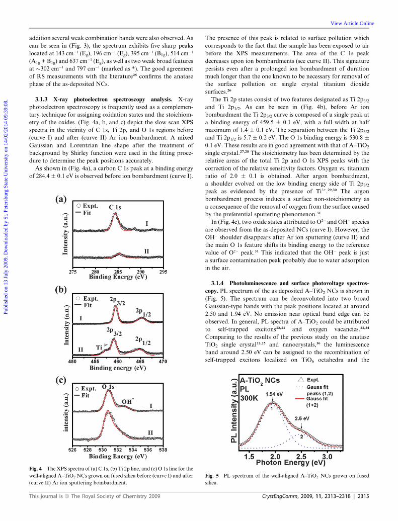
3.1.4 Photoluminescence and surface photovoltage spectros-
copy. PL spectrum of the as deposited A–TiO2 NCs is shown in
(Fig. 5). The spectrum can be deconvoluted into two broad
Gaussian-type bands with the peak positions located at around
2.50 and 1.94 eV. No emission near optical band edge can be
observed. In general, PL spectra of A–TiO2 could be attributed
to self-trapped excitons32,33 and oxygen vacancies.33,34
Comparing to the results of the previous study on the anatase
TiO2 single crystal32,35 and nanocrystals,36 the luminescence
band around 2.50 eV can be assigned to the recombination of
self-trapped excitons localized on TiO6 octahedra and the
Fig. 5 PL spectrum of the well-aligned A–TiO2 NCs grown on fused
silica.
CrystEngComm, 2009, 11, 2313–2318 | 2315

Fig. 6 (a) SPV spectrum of the well-aligned A–TiO2 NCs grown on
fused silica measured at room temperature, (b) SPV spectrum plotted in
coordinate (PVE)1/2 vs. E.
Fig. 7 (a) TEM image of a single A–TiO2 NC, (b) TEM image focused
on top of A–TiO2 NC, (c) the SAED pattern along [1�10]zone axis and (d)
a high-resolution TEM taken from the top of A–TiO2 NC marked in (b).
Publ
ishe
d on
13
July
200
9. D
ownl
oade
d by
St.
Pete
rsbu
rg S
tate
Uni
vers
ity o
n 14
/02/
2014
09:
39:0
8.
View Article Online
dominate emission band at 1.94 eV is attributed to the oxygen
vacancies.
The room-temperature surface photovoltage spectrum for the
as grown A–TiO2 NCs is illustrated in (Fig. 6a). It is well known
that under low power optical excitation the photovoltage (PV)
signal is proportional to the absorption coefficient a multiplied
by the photon flux density F (PV faF).37,38 The photon flux
density F is equivalent to the light intensity I divided by the
photon energy E: F ¼ I/E. Thus, by keeping I constant one has
PV multiplied by the photon energy to be PVE fa. Therefore,
we analyze the SPV spectrum by the relation (PVE)1/2 vs E. The
band gap energy could be obtained by extrapolating the linear
part of the plot (PVE)1/2 vs. E to zero. As shown in (Fig. 6b), the
fit by (PVE)1/2 vs. E yields a satisfactory result which agrees well
with the indirect band character. The indirect band gap of the
A–TiO2 NCs is determined to be 3.14 � 0.01 eV, which is closed
to that of the A–TiO2 single crystal.39
3.1.5 TEM and SAED analysis. Further structural charac-
terizations of the A–TiO2 NCs are studied using the TEM
technique. Fig. 7a shows the TEM image of a single rod-like
A–TiO2 NC. Fig. 7b depicts the SAED pattern taken along the
[1�10] zone axis from the single NC. The TEM image focuses on
the top of A–TiO2 NCs, shown in Fig. 7c is an illustration of the
relationship of the growth plane of the as-deposited NCs. The
high-resolution TEM (HRTEM) image shown in (Fig. 7d) is
taken from the NCs marked by a white square in Fig. 7c. The
HRTEM image exhibits clear and well-defined lattice planes with
lattice spacing of d001 ¼ 0.48 nm for the (001) plane, d110 ¼ 0.28
nm for the (110) plane and d112 ¼ 0.46 nm for the (112) plane.
The lattice spacing of 0.28 nm in the longitudinal direction
corresponds to the d spacing of (110) crystal planes, confirming
the XRD analysis that the A–TiO2 NCs are preferentially
oriented along the [110] direction.
2316 | CrystEngComm, 2009, 11, 2313–2318
3.2 Growth mechanisms
The possible formation mechanisms of the well-aligned A–TiO2
NCs will be discussed as the following. The intrinsic growth
kinetics of A–TiO2 NCs, such as energetically favorable surface
for incoming atoms, can be well accounted for by the periodic
bond chain theory (PBC)40–42 which explains the growth behavior
at the molecular level. Other parameters such as growth condi-
tion are treated as the external factor. It has been determined that
the {112} facets of the A–TiO2 NCs have a larger surface energy
than that of the (110) and (001) planes.42 Accordingly, PBC
dictates that {112} facets will dominate the initial growth of the
well-aligned NCs. From ref. 42 the (001)-oriented plane has been
determined to be denser than the (110) and (112) planes with the
(112) plane being the least dense. The surface bond chain energy
between atoms obeys the relation of (001) plane < (110) plane <
(112) plane, resulting in a preferential growth of atoms bonded
on the (112) plane. In addition, the external factors such as
growth conditions (including growth chamber geometry with
oriented source delivery, growth temperature, pressure etc.) can
also influence the intrinsic factor resulting in the NCs growth
along the preferred orientation. The above mentioned mecha-
nism is quite similar to that of the so-called ‘‘oriented attach-
ment’’ model reported by Penn and Banfield.43 Penn and Banfield
presented the ‘‘oriented attachment’’ mechanism,43 in which the
formation of secondary mono-crystalline particles through
attachments of primary particles in a highly oriented fashion can
take place. This model provides a satisfactorily description of the
growth process of complex-shaped nanostructures using primary
nanoparticles themselves as building blocks. In this process, the
bigger particles are grown from small primary nanoparticles
through an oriented attachment mechanism, in which the adja-
cent nanoparticles are self-assembled by sharing a common
crystallographic orientation and attachment of these particles at
This journal is ª The Royal Society of Chemistry 2009

Publ
ishe
d on
13
July
200
9. D
ownl
oade
d by
St.
Pete
rsbu
rg S
tate
Uni
vers
ity o
n 14
/02/
2014
09:
39:0
8.
View Article Online
a planar interface.44,45 The driving force for this spontaneous
oriented attachment is that the elimination of the pairs of high
energy surfaces will lead to a substantial reduction in the surface
free energy from the thermodynamic viewpoint. This viewpoint
agreed with the PBC description where the anisotropic growth of
nanoparticles is on crystallographic planes of a larger surface
energy.
The magnified FESEM images from Fig. 2a are shown in
Fig. 8a, b, c and d. From Fig. 8a and c, the columnar structure
consists of many building units with each building unit being
parallel to the C-plane on top of the A–TiO2 NCs. The cross
sectional view of the columnar structure is illustrated in Fig. 8b
and d. The alignment of the observed columnar layers can be
understood as follows: According to the PBC theory, higher
surface volume density leads to a lower growth rate. Under such
circumstances, the building unit of the same {112} facets will
bond to initiate the growth process. As the growth process
proceeds, the dominant (112) oriented building units can bond
periodically to complete the observed columnar structure.
Schematic diagrams illustrating the growth behavior as described
by the PBC theory are shown in Fig. 8e and f. The preferable
growth plane with {112} facets also explains the symmetric
Fig. 8 (a) Tilt view (30�), (b) cross-sectional view, (c) enlarged tilt view,
and (d) enlarged cross-sectional view of FESEM image focused on
a single A–TiO2 NC. (e) and (f) The schematic diagrams of the growth
behavior of A–TiO2 NC as described by the PBC theory.
This journal is ª The Royal Society of Chemistry 2009
columnar layers as observed along the [110] direction. The rela-
tionship as schematically illustrated in Fig. 8f is supported by the
XRD and the SAED analyses.
4. Conclusions
The well-aligned A–TiO2 NCs were grown on fused silica by
cold-wall MOCVD using Ti(OC3H7)4 as a source reagent.
FESEM micrographs showed that the growth of vertically
aligned NCs, XRD pattern revealed A–TiO2 aligned in a prefer-
ential orientation of (220), the Raman spectrum confirmed
deposition of pure anatase phase TiO2. Luminescence of self-
trapped excitons and oxygen vacancies were observed in anatase
NCs. The indirect band gap of A–TiO2 was determined to be
3.14 � 0.01 eV by SPS measurement. EDX and XPS analyses
showed an oxygen vs. titanium ratio of 2.0� 0.1 for the deposited
TiO2 NCs. The structural characterization of the well-aligned
A–TiO2 NCs via FESEM, XRD, TEM and SAED revealed the
formation of building units bonded along {112} facets with
preferred (220) orientation. The growth behavior, as described
by the PBC theory and the external factors such as growth
conditions resulting in the growth of NCs along a preferable
orientation, can also be well explained by the oriented attach-
ment mechanism.
Acknowledgements
The authors acknowledge the support of the National Science
Council of Taiwan under Nos. NSC 96-2112-M-011-001 and
NSC 97-2112-M-011-001-My3.
References
1 A. Fujishima, T. N. Rao and A. Tryk, J. Photochem. Photobiol., C,2000, 1, 1–21.
2 C. Garzella, E. Comini, E. Tempesti, C. Frigeri and G. Sberveglieri,Sens. Actuators, B, 2000, 68, 189–196.
3 B. O’Regan and M. Gr€atzel, Nature, 1991, 353, 737–740.4 A. Richel, N. P. Johnson and D. W. McComb, Appl. Phys. Lett.,
2000, 76, 1816–1818.5 Z. Miao, D. Xu, J. Ouyang, G. Guo, X. Zhao and Y. Tang, Nano
Lett., 2002, 2, 717–720.6 S. Cerneaux, X. Xiong, G. P. Simon, Y. B. Cheng and L. Spiccia,
Nanotechnology, 2007, 18, 055708.7 D. Liu and M. Z. Yates, Langmuir, 2007, 23, 10333–10341.8 W. F. Zhang, M. S. Zhang and Z. Yin, Phys. Status Solidi A, 2000,
179, 319–327.9 S. Qourzal, A. Assabbane and Y. Ait-Ichou, J. Photochem., A: Chem.,
2004, 163, 317–321.10 J. M. Wu, H. C. Shih and W. T. Wu, J. Vac. Sci. Technol., B, 2005, 23,
2122–2126.11 J. M. Wu, H. C. Shih and W. T. Wu, Chem. Phys. Lett., 2005, 413,
490–494.12 J. M. Wu, W. T. Wu and H. C. Shih, J. Electrochem. Soc., 2005, 152,
G613–G616.13 J. J. Wu and C. C. Yu, J. Phys. Chem. B, 2004, 108, 3377–3379.14 P. Evans, M. E. Pemble and D. W. Shell, Chem. Mater., 2006, 18,
5750–5755.15 L. A. Brook, P. Evans, H. A. Foster, M. E. Pemble, A. Steele,
D. W. Shell and H. M. Yates, J. Photochem. A: Chem., 2005, 187,53–63.
16 M. K. Lee, J. J. Huang and T. S. Wu, Semicond. Sci. Technol., 2005,20, 519–523.
17 R. J. Puddephatt, Polyhedron, 1994, 13, 1233–1243.18 F. Maury, Chem. Vap. Deposition, 1996, 2, 113–116.19 C. A. Chen, A. Korotcov, Y. M. Chen, Y. S. Huang, D. S. Tsai,
K. K. Tiong and P. C. Liao, ECS Trans., 2008, 11, 19–25.
CrystEngComm, 2009, 11, 2313–2318 | 2317

Publ
ishe
d on
13
July
200
9. D
ownl
oade
d by
St.
Pete
rsbu
rg S
tate
Uni
vers
ity o
n 14
/02/
2014
09:
39:0
8.
View Article Online
20 R. S. Chen, Y. S. Huang, Y. M. Liang, C. S. Hsieh, D. S. Tsai andK. K. Tiong, Appl. Phys. Lett., 2004, 84, 1552–1554.
21 L. Aigouy, F. H. Pollark, J. Petruzzello and K. Shahzad, Solid StateCommun., 1997, 102, 877–882.
22 H. P. Hsu, P. Y. Wu, Y. S. Huang, S. Sanorphim, K. K. Tiong,R. Katayamaand K. Onabe, J. Phys.: Condens. Matter, 2007, 19, 096009.
23 R. W. G. Wyckoff, Crystal Structures, Interscience Publishers, NewYork, 1965, Vol. 1, pp. 253–265.
24 R. Loudon, Adv. Phys., 1964, 13, 423–482.25 T. Ohsaka, F. Izumi and Y. Fujiki, J. Raman Spectrosc., 1978, 7, 321–
323.26 S. Bourgeois, P. Le. Seigneur and M. Perdreau, Surf. Sci., 1995, 328,
105–110.27 G. Y. Hua, H. S. Cheng, Y. I. Shi, Z. Jin, L. Gang, C. S. Sean,
M. C. Hui and Q. L. Gao, Nature, 2008, 453, 638–641.28 G. Silversmit, G. D. Doncker and R. D. Gryse, Surf. Sci. Spectrosc.,
2002, 9, 21–29.29 W. G€opel, J. A. Anderson, D. Frankel, M. Jaehnig, K. Phillips,
J. A. Sch€affer and G. Rocker, Surf. Sci., 1984, 139, 333–346.30 P. Stefanov, M. Shipochka, P. Stefchev, Z. Raicheva, V. Lazarova
and L. Spassov, J. Phys.: Conf. Ser., 2008, 100, 012039–012043.31 G. Betz and G. K. Wehner, Sputtering by Particle Bombardment II, in
Topics in Applied Physics, ed. R. Behrisch, Springer-Verlag, Berlin,1983, Vol. 52, pp. 11–90.
2318 | CrystEngComm, 2009, 11, 2313–2318
32 H. Tang, H. Berger, P. Schmid and F. L�evy, Solid State Commun.,1993, 87, 847–850.
33 L. V. Saraf, S. I. Patil, S. B. Ogale, S. R. Sainkar and S. T. Kshirsager,Int. J. Mod. Phys. B, 1998, 12, 2635–2647.
34 N. Serpone, D. Lawless and R. Khairutdinov, J. Phys. Chem., 1995,99, 16646–16654.
35 T. Sekiya, S. Kamei and S. Kurita, J. Lumin., 2000, 87–89, 1140–1142.36 J. M. Wu, H. C. Shin, W. T. Wu, Y. K. Tseng and I. C. Chen, J. Cryst.
Growth, 2005, 281, 384–390.37 L. Kronik and Y. Shapira, Surf. Sci. Rep., 1999, 37, 1–206.38 Gh. Dumitras, H. Riechert, H. Porteanu and F. Koch, Phys. Rev. B,
2002, 66, 205324–205331.39 N. Hosaka, T. Sekiya and S. Kurita, J. Lumin., 1997, 72–74, 874–875.40 P. Hartman, Crystal Growth: An Introduction, North Holland
Publishing Company, Amsterdam, 1973, Vol. 1, pp. 403–443.41 I. Sunagawa, Morphology of Crystals, Terra Scientific Publishing
Company, Tokyo, 1987, Vol. A, pp. 77–206.42 B. Kim, D. Byun, J. K. Lee and D. Park, Jpn. J. Appl. Phys., Part 1,
2001, 41, 222–226.43 R. L. Penn and J. F. Banfield, Science, 1998, 281, 969–971.44 Q. Zhang, S. J. Liu and S. H. Yu, J. Mater. Chem., 2009, 19, 191–
207.45 M. Adachi, Y. Murata, J. Takao, J. Jiu, M. Sakamoto and F. Wang,
J. Am. Chem. Soc., 2004, 126, 14943–14949.
This journal is ª The Royal Society of Chemistry 2009