Embed Size (px)
Citation preview
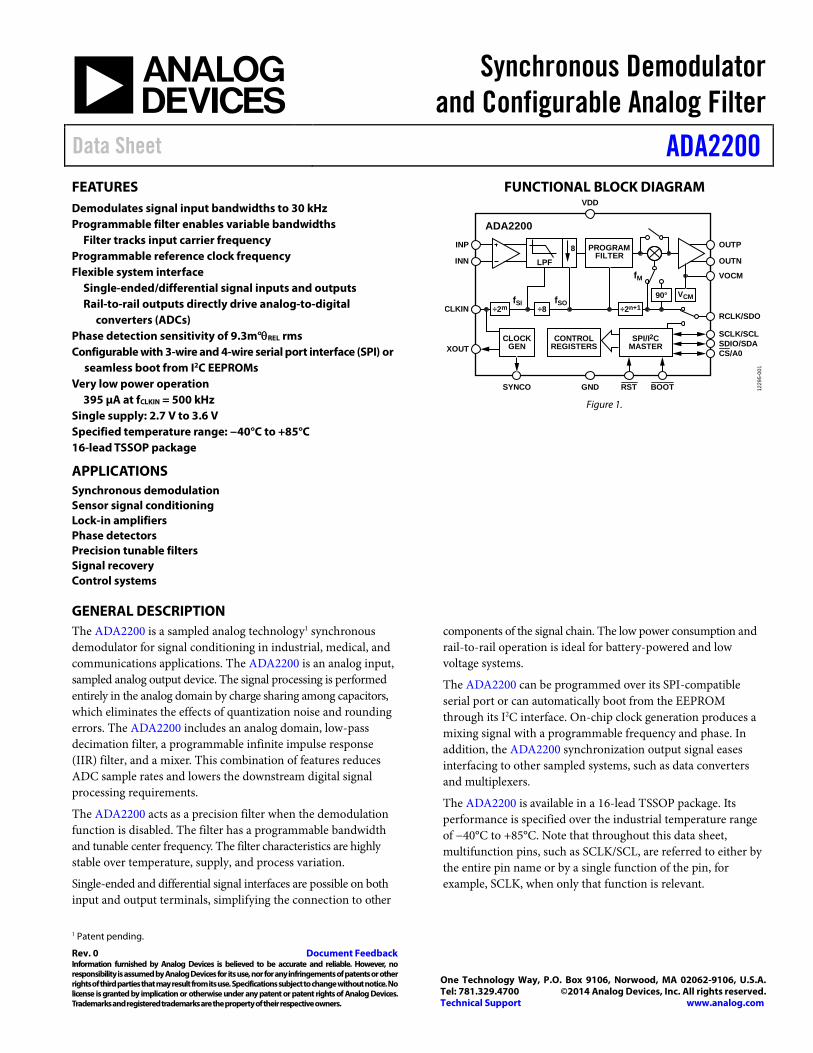
Synchronous Demodulator and Configurable Analog Filter
Data Sheet ADA2200
FEATURES Demodulates signal input bandwidths to 30 kHz Programmable filter enables variable bandwidths
Filter tracks input carrier frequency Programmable reference clock frequency Flexible system interface
Single-ended/differential signal inputs and outputs Rail-to-rail outputs directly drive analog-to-digital
converters (ADCs) Phase detection sensitivity of 9.3m°θREL rms Configurable with 3-wire and 4-wire serial port interface (SPI) or
seamless boot from I2C EEPROMs Very low power operation
395 μA at fCLKIN = 500 kHz Single supply: 2.7 V to 3.6 V Specified temperature range: −40°C to +85°C 16-lead TSSOP package
APPLICATIONS Synchronous demodulation Sensor signal conditioning Lock-in amplifiers Phase detectors Precision tunable filters Signal recovery Control systems
FUNCTIONAL BLOCK DIAGRAM
Figure 1.
GENERAL DESCRIPTION The ADA2200 is a sampled analog technology1 synchronous demodulator for signal conditioning in industrial, medical, and communications applications. The ADA2200 is an analog input, sampled analog output device. The signal processing is performed entirely in the analog domain by charge sharing among capacitors, which eliminates the effects of quantization noise and rounding errors. The ADA2200 includes an analog domain, low-pass decimation filter, a programmable infinite impulse response (IIR) filter, and a mixer. This combination of features reduces ADC sample rates and lowers the downstream digital signal processing requirements.
The ADA2200 acts as a precision filter when the demodulation function is disabled. The filter has a programmable bandwidth and tunable center frequency. The filter characteristics are highly stable over temperature, supply, and process variation.
Single-ended and differential signal interfaces are possible on both input and output terminals, simplifying the connection to other
components of the signal chain. The low power consumption and rail-to-rail operation is ideal for battery-powered and low voltage systems.
The ADA2200 can be programmed over its SPI-compatible serial port or can automatically boot from the EEPROM through its I2C interface. On-chip clock generation produces a mixing signal with a programmable frequency and phase. In addition, the ADA2200 synchronization output signal eases interfacing to other sampled systems, such as data converters and multiplexers.
The ADA2200 is available in a 16-lead TSSOP package. Its performance is specified over the industrial temperature range of −40°C to +85°C. Note that throughout this data sheet, multifunction pins, such as SCLK/SCL, are referred to either by the entire pin name or by a single function of the pin, for example, SCLK, when only that function is relevant.
1 Patent pending.
INP
INN
OUTP
OUTN
VOCM
SCLK/SCLSDIO/SDACS/A0
RCLK/SDO
VDD
LPF
8 PROGRAMFILTER
CLOCKGEN
CONTROLREGISTERS
SPI/I2CMASTER
VCM
÷2n+1÷2m ÷890°fSOfSI
fM
XOUT
CLKIN
SYNCO GND RST BOOT
ADA2200
1229
5-00
1
Rev. 0 Document Feedback Information furnished by Analog Devices is believed to be accurate and reliable. However, no responsibility is assumed by Analog Devices for its use, nor for any infringements of patents or other rights of third parties that may result from its use. Specifications subject to change without notice. No license is granted by implication or otherwise under any patent or patent rights of Analog Devices. Trademarks and registered trademarks are the property of their respective owners.
One Technology Way, P.O. Box 9106, Norwood, MA 02062-9106, U.S.A. Tel: 781.329.4700 ©2014 Analog Devices, Inc. All rights reserved. Technical Support www.analog.com
ADA2200 Data Sheet
TABLE OF CONTENTS Features .............................................................................................. 1 Applications ....................................................................................... 1 Functional Block Diagram .............................................................. 1 General Description ......................................................................... 1 Revision History ............................................................................... 2 Specifications ..................................................................................... 3
SPI Timing Characteristics ......................................................... 4 Absolute Maximum Ratings ............................................................ 7
Thermal Resistance ...................................................................... 7 ESD Caution .................................................................................. 7
Pin Configuration and Function Descriptions ............................. 8 Typical Performance Characteristics ............................................. 9 Terminology .................................................................................... 10 Theory of Operation ...................................................................... 11
Synchronous Demodulation Basics ......................................... 11 ADA2200 Architecture .............................................................. 12 Decimation Filter........................................................................ 12 IIR Filter ....................................................................................... 13 Mixer ............................................................................................ 13 Clocking Options ....................................................................... 14
Input and Output Amplifiers .................................................... 15 Applications Information .............................................................. 16
Amplitude Measurements ......................................................... 16 Phase Measurements .................................................................. 16 Amplitude and Phase Measurements ...................................... 16 Analog Output Systems ............................................................. 17 Interfacing to ADCs ................................................................... 17 Lock-In Amplifier Application ................................................. 17 Interfacing to Microcontrollers ................................................ 18 EEPROM Boot Configuration .................................................. 18 Power Dissipation....................................................................... 18
Device Configuration .................................................................... 19 Serial Port Operation ................................................................. 19 Data Format ................................................................................ 19 Serial Port Pin Descriptions ...................................................... 19 Serial Port Options ..................................................................... 19 Booting from EEPROM ............................................................ 20
Device Configuration Register Map and Descriptions ............. 21 Outline Dimensions ....................................................................... 24 Ordering Guide ............................................................................... 24
REVISION HISTORY 8/14—Revision 0: Initial Version
Rev. 0 | Page 2 of 24
Data Sheet ADA2200
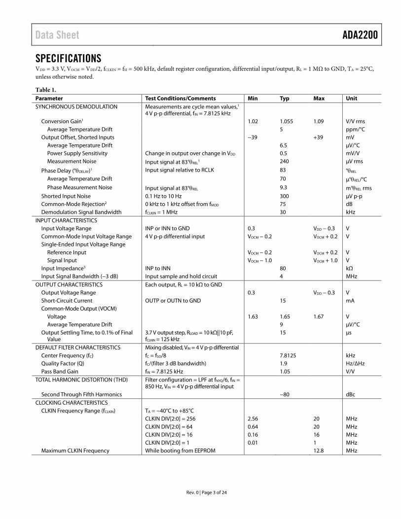
SPECIFICATIONS VDD = 3.3 V, VOCM = VDD/2, fCLKIN = fSI = 500 kHz, default register configuration, differential input/output, RL = 1 MΩ to GND, TA = 25°C, unless otherwise noted.
Table 1. Parameter Test Conditions/Comments Min Typ Max Unit SYNCHRONOUS DEMODULATION Measurements are cycle mean values,1
4 V p-p differential, fIN = 7.8125 kHz
Conversion Gain1 1.02 1.055 1.09 V/V rms
Average Temperature Drift 5 ppm/°C Output Offset, Shorted Inputs −39 +39 mV
Average Temperature Drift 6.5 μV/°C Power Supply Sensitivity Change in output over change in VDD 0.5 mV/V Measurement Noise Input signal at 83°θREL
1 240 μV rms
Phase Delay (°θDELAY)1 Input signal relative to RCLK 83 °θREL Average Temperature Drift 70 μ°θREL/°C Phase Measurement Noise Input signal at 83°θREL 9.3 m°θREL rms
Shorted Input Noise 0.1 Hz to 10 Hz 300 μV p-p Common-Mode Rejection2 0 kHz to 1 kHz offset from fMOD 75 dB Demodulation Signal Bandwidth fCLKIN = 1 MHz 30 kHz
INPUT CHARACTERISTICS Input Voltage Range INP or INN to GND 0.3 VDD − 0.3 V Common-Mode Input Voltage Range 4 V p-p differential input VOCM − 0.2 VOCM + 0.2 V Single-Ended Input Voltage Range
Reference Input VOCM − 0.2 VOCM + 0.2 V Signal Input VOCM − 1.0 VOCM + 1.0 V
Input Impedance3 INP to INN 80 kΩ Input Signal Bandwidth (−3 dB) Input sample and hold circuit 4 MHz
OUTPUT CHARACTERISTICS Each output, RL = 10 kΩ to GND Output Voltage Range 0.3 VDD − 0.3 V Short-Circuit Current OUTP or OUTN to GND 15 mA Common-Mode Output (VOCM)
Voltage 1.63 1.65 1.67 V Average Temperature Drift 9 μV/°C
Output Settling Time, to 0.1% of Final Value
3.7 V output step, RLOAD = 10 kΩ||10 pF, fCLKIN = 125 kHz
15 μs
DEFAULT FILTER CHARACTERISTICS Mixing disabled, VIN = 4 V p-p differential Center Frequency (fC) fC = fSO/8 7.8125 kHz Quality Factor (Q) fC/(filter 3 dB bandwidth) 1.9 Hz/ΔHz Pass Band Gain fIN = 7.8125 kHz 1.05 V/V
TOTAL HARMONIC DISTORTION (THD) Filter configuration = LPF at fNYQ/6, fIN = 850 Hz, VIN = 4 V p-p differential input
Second Through Fifth Harmonics −80 dBc CLOCKING CHARACTERISTICS
CLKIN Frequency Range (fCLKIN) TA = −40°C to +85°C CLKIN DIV[2:0] = 256 2.56 20 MHz
CLKIN DIV[2:0] = 64 0.64 20 MHz CLKIN DIV[2:0] = 16 0.16 16 MHz
CLKIN DIV[2:0] = 1 0.01 1 MHz Maximum CLKIN Frequency While booting from EEPROM 12.8 MHz
Rev. 0 | Page 3 of 24
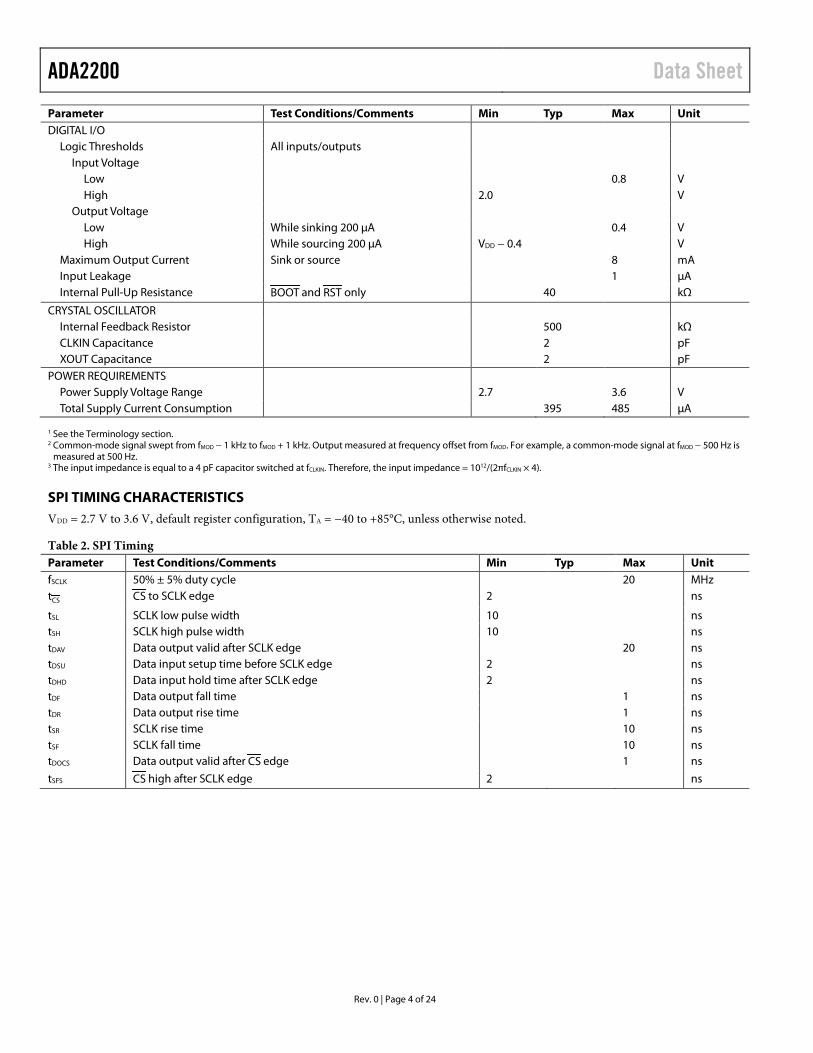
ADA2200 Data Sheet
Parameter Test Conditions/Comments Min Typ Max Unit DIGITAL I/O
Logic Thresholds All inputs/outputs Input Voltage
Low 0.8 V High 2.0 V
Output Voltage Low While sinking 200 µA 0.4 V High While sourcing 200 µA VDD − 0.4 V
Maximum Output Current Sink or source 8 mA Input Leakage 1 µA Internal Pull-Up Resistance BOOT and RST only 40 kΩ
CRYSTAL OSCILLATOR Internal Feedback Resistor 500 kΩ CLKIN Capacitance 2 pF XOUT Capacitance 2 pF
POWER REQUIREMENTS Power Supply Voltage Range 2.7 3.6 V Total Supply Current Consumption 395 485 µA
1 See the Terminology section. 2 Common-mode signal swept from fMOD − 1 kHz to fMOD + 1 kHz. Output measured at frequency offset from fMOD. For example, a common-mode signal at fMOD − 500 Hz is
measured at 500 Hz. 3 The input impedance is equal to a 4 pF capacitor switched at fCLKIN. Therefore, the input impedance = 1012/(2πfCLKIN × 4).
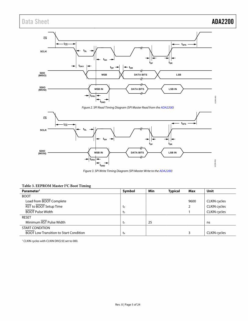
SPI TIMING CHARACTERISTICS VDD = 2.7 V to 3.6 V, default register configuration, TA = −40 to +85°C, unless otherwise noted.
Table 2. SPI Timing Parameter Test Conditions/Comments Min Typ Max Unit fSCLK 50% ± 5% duty cycle 20 MHz tCS CS to SCLK edge 2 ns
tSL SCLK low pulse width 10 ns tSH SCLK high pulse width 10 ns tDAV Data output valid after SCLK edge 20 ns tDSU Data input setup time before SCLK edge 2 ns tDHD Data input hold time after SCLK edge 2 ns tDF Data output fall time 1 ns tDR Data output rise time 1 ns tSR SCLK rise time 10 ns tSF SCLK fall time 10 ns tDOCS Data output valid after CS edge 1 ns
tSFS CS high after SCLK edge 2 ns
Rev. 0 | Page 4 of 24
Data Sheet ADA2200
Figure 2. SPI Read Timing Diagram (SPI Master Read from the ADA2200)
Figure 3. SPI Write Timing Diagram (SPI Master Write to the ADA2200)
Table 3. EEPROM Master I2C Boot Timing Parameter1 Symbol Min Typical Max Unit BOOT
Load from BOOT Complete 9600 CLKIN cycles
RST to BOOT Setup Time t2 2 CLKIN cycles
BOOT Pulse Width t3 1 CLKIN cycles
RESET Minimum RST Pulse Width t1 25 ns
START CONDITION BOOT Low Transition to Start Condition t4 3 CLKIN cycles
1 CLKIN cycles with CLKIN DIV[2:0] set to 000.
SCLK
CS
SDO(MISO) MSB DATA BITS LSB
SDIO(MOSI) MSB IN DATA BITS LSB IN
tSL
tCS
tSH
tSFS
tSF tSR
tDRtDFtDAV
tDSU
tDHD 1229
5-00
3
SCLK
CS
SDIO(MOSI) MSB IN DATA BITS LSB IN
tSL
tCS
tSH
tSFS
tSF tSR
tDSU
tDHD 1229
5-00
4
Rev. 0 | Page 5 of 24
ADA2200 Data Sheet
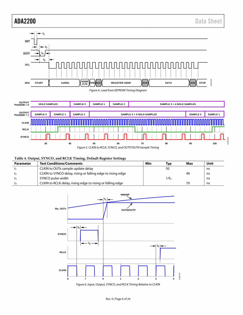
Figure 4. Load from EEPROM Timing Diagram
Figure 5. CLKIN to RCLK, SYNCO, and OUTP/OUTN Sample Timing
Table 4. Output, SYNCO, and RCLK Timing, Default Register Settings Parameter Test Conditions/Comments Min Typ Max Unit t1 CLKIN to OUTx sample update delay 50 ns t2 CLKIN to SYNCO delay, rising or falling edge to rising edge 40 ns t3 SYNCO pulse width 1/fSI ns t4 CLKIN to RCLK delay, rising edge to rising or falling edge 70 ns
Figure 6. Input, Output, SYNCO, and RCLK Timing Relative to CLKIN
t1
t2
t3
t4
RST
BOOT
SCL
SDA START b10001 R/W ACK ACK ACKDATA STOPREGISTER ADDRADDR[1:0]
1229
5-00
5
30
SAMPLE 0 SAMPLE 1 SAMPLE 2 SAMPLE 3 + 4 HOLD SAMPLES
40 50 60 70 80 90 100
OUTPUTPHASE90 = 1
CLKIN
RCLK
SYNCO
1229
5-00
6
HOLD SAMPLES
SAMPLE 0 SAMPLE 1 SAMPLE 2 SAMPLE 3 + 4 HOLD SAMPLES SAMPLE 0 SAMPLE 1
OUTPUTPHASE90 = 0
6
CLKIN
RCLK
SYNCO
INx, OUTx
INN/INP
OUTN/OUTP
7 0 1 2 3 4
t1
t2
t3 t4
1229
5-00
7
Rev. 0 | Page 6 of 24
Data Sheet ADA2200
ABSOLUTE MAXIMUM RATINGS Table 5. Parameter Rating Supply Voltage 3.9 V Output Short-Circuit Current Duration Indefinite Maximum Voltage at Any Input VDD + 0.3 V Minimum Voltage at Any Input GND − 0.3 V Operational Temperature Range −40°C to +125°C Storage Temperature Range −65°C to +150°C Package Glass Transition Temperature 150°C ESD Ratings
Human Body Model (HBM) 1000 V Device Model (FICDM) 500 V Machine Model (MM) 50 V
Stresses at or above those listed under Absolute Maximum Ratings may cause permanent damage to the product. This is a stress rating only; functional operation of the product at these or any other conditions above those indicated in the operational section of this specification is not implied. Operation beyond the maximum operating conditions for extended periods may affect product reliability.
THERMAL RESISTANCE θJA is specified for a device in a natural convection environment, soldered on a 4-layer JEDEC printed circuit board (PCB).
Table 6. Package θJA θJC Unit 16-Lead TSSOP 100 14.8 °C/W
ESD CAUTION
Rev. 0 | Page 7 of 24
ADA2200 Data Sheet
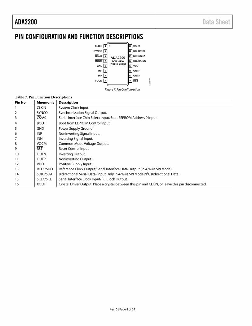
PIN CONFIGURATION AND FUNCTION DESCRIPTIONS
Figure 7. Pin Configuration
Table 7. Pin Function Descriptions Pin No. Mnemonic Description 1 CLKIN System Clock Input. 2 SYNCO Synchronization Signal Output. 3 CS/A0 Serial Interface Chip Select Input/Boot EEPROM Address 0 Input.
4 BOOT Boot from EEPROM Control Input.
5 GND Power Supply Ground. 6 INP Noninverting Signal Input. 7 INN Inverting Signal Input. 8 VOCM Common-Mode Voltage Output. 9 RST Reset Control Input.
10 OUTN Inverting Output. 11 OUTP Noninverting Output. 12 VDD Positive Supply Input. 13 RCLK/SDO Reference Clock Output/Serial Interface Data Output (in 4-Wire SPI Mode). 14 SDIO/SDA Bidirectional Serial Data (Input Only in 4-Wire SPI Mode)/I2C Bidirectional Data. 15 SCLK/SCL Serial Interface Clock Input/I2C Clock Output. 16 XOUT Crystal Driver Output. Place a crystal between this pin and CLKIN, or leave this pin disconnected.
1
2
3
4
5
6
7
8
16
15
14
13
12
11
10
9
SYNCO
CS/A0
BOOT
INN
INP
GND
CLKIN
SCLK/SCL
SDIO/SDA
RCLK/SDO
OUTN
VOCM RST
OUTP
VDD
XOUT
ADA2200TOP VIEW
(Not to Scale)
1229
5-00
8
Rev. 0 | Page 8 of 24
0
5
10
15
20
25
30
35
78 79 80 81 82 83 84
NU
MB
ER
OF
HIT
S
RELATIVE PHASE (Degrees)1
22
95
-10
9
–0.20
–0.15
–0.10
–0.05
0
0.05
0.10
0 10 20 30 40 50 60
SE
TT
LIN
G E
RR
OR
(%
)
TIME (µs)
12
29
5-1
10
–10
–5
0
5
10
15
20
25
30
35
–270 –240 –210 –180 –150 –120 –90 –60 –30 0 30 60 90
MA
GN
ITU
DE
ER
RO
R (
mV
)
RELATIVE PHASE (Degrees)
12
29
5-1
14
MAGNITUDE ERROR
MAGNITUDE ERROR, OFFSET REMOVED
–200
–150
–100
–50
0
50
100
150
200
0 10987654321
OU
TP
UT
NO
ISE
(µ
V)
TIME (Seconds)
12
29
5-1
12
100
1k
10k
1 100k10k1k10010
NO
ISE
SP
EC
TR
AL
DE
NS
ITY
(n
V/√
Hz)
FREQUENCY (Hz)
12
29
5-1
13
CLKIN = 500kHz
–1.0
–0.8
–0.6
–0.4
–0.2
0
0.2
0.4
0.6
0.8
1.0
–270 –240 –210 –180 –150 –120 –90 –60 –30 0 30 60 90
PH
AS
E M
EA
SU
RE
ME
NT
ER
RO
R (
Deg
rees)
RELATIVE PHASE (Degrees)
12
29
5-1
11
PHASE ERROR
PHASE ERROR, OFFSET REMOVED
ADA2200 Data Sheet
TERMINOLOGY Cycle Mean The cycle mean is the average of all the output samples (OUTP/OUTN) over one RCLK period. In the default configuration, there are eight output samples per RCLK cycle; thus, the cycle mean is the average of eight consecutive output samples. If the device is reconfigured such that the frequency of RCLK is fSO/4, then the cycle mean is the average of four consecutive output samples.
Conversion Gain Conversion gain is calculated as follows:
INV
QIGainConversion
22 +=
where: I is the offset corrected cycle mean, PHASE90 bit = 0. Q is the offset corrected cycle mean, PHASE90 bit = 1. VIN is the rms value of the input voltage.
The offset corrected cycle mean = cycle mean − output offset.
Relative Phase (θREL) Relative phase is the phase difference between the rising positive zero crossing of a sine wave at the INN/INP inputs relative to the next rising edge of RCLK.
Figure 14. Example Showing Relative Phase, θREL, of 37°
Phase Delay (°θDELAY) The phase delay is the relative phase (θREL) that produces a zero cycle mean output value for a sine wave input with a frequency equal to fRCLK. The phase delay is the relative phase value that corresponds to the positive zero crossing of the phase measurement transfer function.
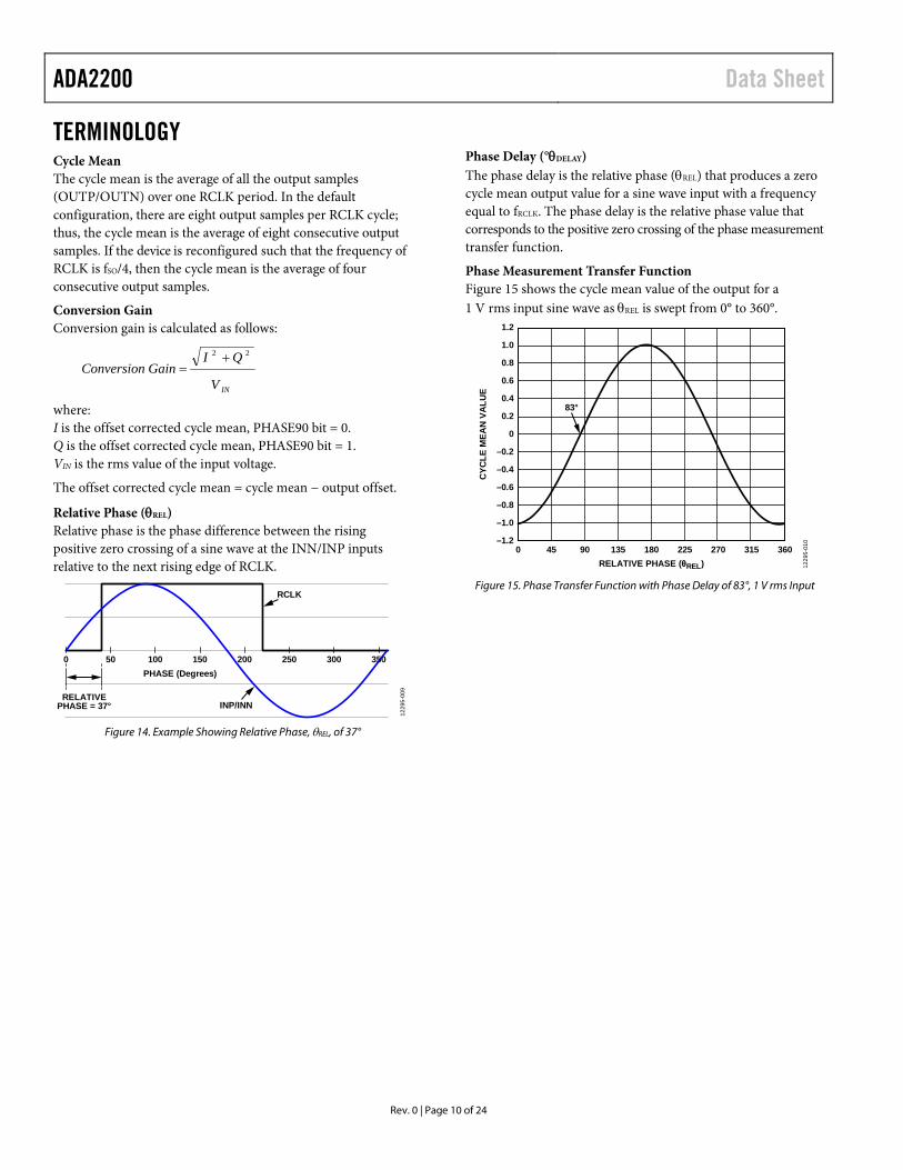
Phase Measurement Transfer Function Figure 15 shows the cycle mean value of the output for a 1 V rms input sine wave as θREL is swept from 0° to 360°.
Figure 15. Phase Transfer Function with Phase Delay of 83°, 1 V rms Input
0 50 100 150 200 250 300 350
RCLK
INP/INN
PHASE (Degrees)
RELATIVEPHASE = 37°
1229
5-00
9
1.2
–1.2
–1.0
–0.8
–0.6
–0.4
–0.2
0
0.2
0.4
0.6
0.8
1.0
0 45 90
83°
135 180 225 270 315 360
CYC
LE M
EAN
VA
LUE
RELATIVE PHASE (θREL) 1229
5-01
0
Rev. 0 | Page 10 of 24
Data Sheet ADA2200
THEORY OF OPERATION The ADA2200 is a synchronous demodulator and tunable filter implemented with sampled analog technology (SAT). Synchronous demodulators, also known as lock-in amplifiers, enable accurate measurement of small ac signals in the presence of noise interference orders of magnitude greater than the signal amplitude. Synchronous demodulators use phase sensitive detection to isolate the component of the signal at a specific reference frequency and phase. Noise at frequencies that are offset from the reference frequency are easily rejected and do not significantly impair the measurement.
SAT works on the principle of charge sharing. A sampled analog signal is a stepwise continuous signal without amplitude quantization. This contrasts with a signal sampled by an ADC, which becomes a discrete time signal with quantized amplitude.
With SAT, the input signal is sampled by holding the voltage on a capacitor at the sampling instant. Basic signal processing can then be performed in the analog domain by charge sharing among capacitors. The ADA2200 includes an analog domain low-pass decimation filter, a programmable IIR filter, and a mixer. This combination of features enables reduced ADC sample rates and lowers the downstream digital signal processing requirements if the signal is digitized.
The output of the ADA2200 can also be used in an all analog signal path. In these applications, add a reconstruction filter following the ADA2200 in the signal path.
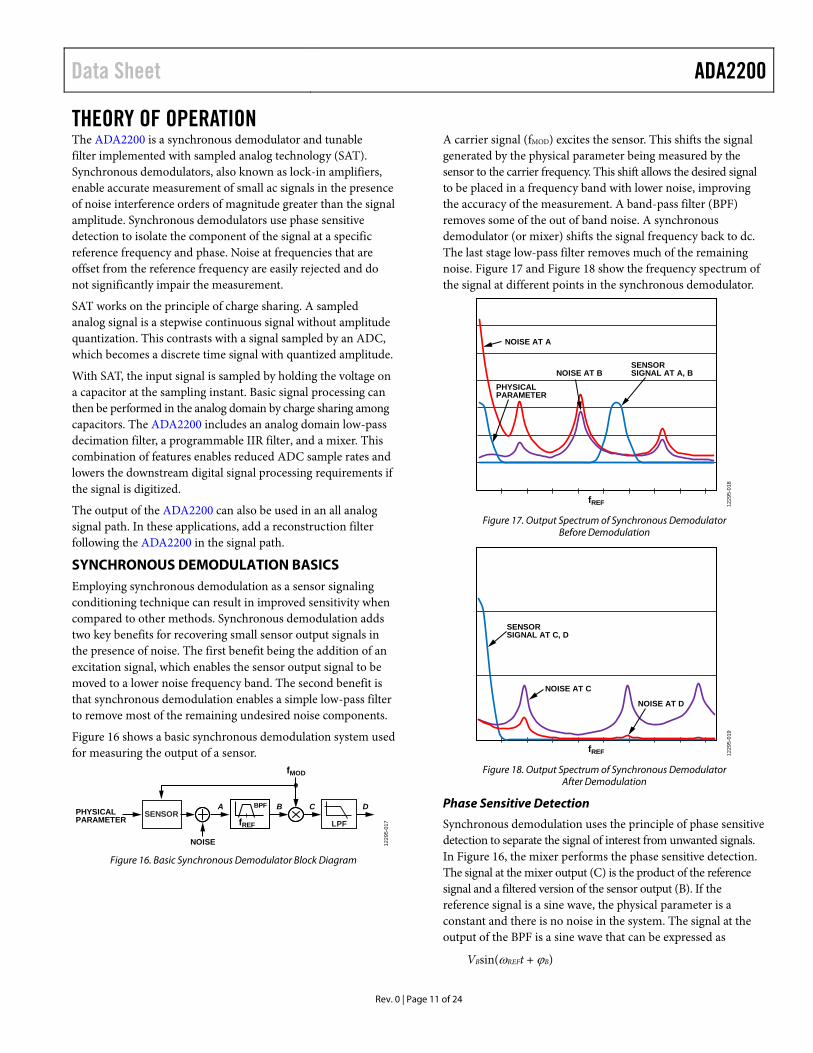
SYNCHRONOUS DEMODULATION BASICS Employing synchronous demodulation as a sensor signaling conditioning technique can result in improved sensitivity when compared to other methods. Synchronous demodulation adds two key benefits for recovering small sensor output signals in the presence of noise. The first benefit being the addition of an excitation signal, which enables the sensor output signal to be moved to a lower noise frequency band. The second benefit is that synchronous demodulation enables a simple low-pass filter to remove most of the remaining undesired noise components.
Figure 16 shows a basic synchronous demodulation system used for measuring the output of a sensor.
Figure 16. Basic Synchronous Demodulator Block Diagram
A carrier signal (fMOD) excites the sensor. This shifts the signal generated by the physical parameter being measured by the sensor to the carrier frequency. This shift allows the desired signal to be placed in a frequency band with lower noise, improving the accuracy of the measurement. A band-pass filter (BPF) removes some of the out of band noise. A synchronous demodulator (or mixer) shifts the signal frequency back to dc. The last stage low-pass filter removes much of the remaining noise. Figure 17 and Figure 18 show the frequency spectrum of the signal at different points in the synchronous demodulator.
Figure 17. Output Spectrum of Synchronous Demodulator
Before Demodulation
Figure 18. Output Spectrum of Synchronous Demodulator
After Demodulation
Phase Sensitive Detection
Synchronous demodulation uses the principle of phase sensitive detection to separate the signal of interest from unwanted signals. In Figure 16, the mixer performs the phase sensitive detection. The signal at the mixer output (C) is the product of the reference signal and a filtered version of the sensor output (B). If the reference signal is a sine wave, the physical parameter is a constant and there is no noise in the system. The signal at the output of the BPF is a sine wave that can be expressed as
VBsin(ωREFt + ϕB)
LPFSENSORPHYSICAL
PARAMETER
NOISE
fMOD
A B C D
fREF
BPF
1229
5-01
7
fREF
NOISE AT A
SENSORSIGNAL AT A, BNOISE AT B
PHYSICALPARAMETER
1229
5-01
8
fREF
NOISE AT D
NOISE AT C
SENSORSIGNAL AT C, D
1229
5-01
9
Rev. 0 | Page 11 of 24
ADA2200 Data Sheet The output of the mixer (if implemented as a multiplier) is then
½VBVREFcos(ϕB − ϕREF) − ½VBVREFcos(2ωREFt + ϕB + ϕREF)
This signal is a dc signal and an ac signal at twice the reference frequency. If the LPF is sufficient to remove the ac signal, the signal at the LPF output (D) is
½VBVREFcos(ϕB − ϕREF)
The LPF output is a dc signal that is proportional to both the magnitude and phase of the signal at the BPF output (B). When the input amplitude is held constant, the LPF output enables can be used to measure the phase. When the input phase is held constant, the LPF can be used to measure amplitude.
Note that the reference signal is not required to be a pure sine wave. The excitation signal and demodulation signal must only share a common frequency and phase to employ phase sensitive detection. In some applications, it may be possible to use the square wave output from the ADA2200 RCLK output directly.
Internal to the ADA2200, the demodulation is performed not by multiplying the REFCLK signal with the input signal, but by holding the output constant for ½ the sample output periods. This operation is similar to a half wave demodulation of the input signal. For more information on signal detection using this function, see the Applications Information section.
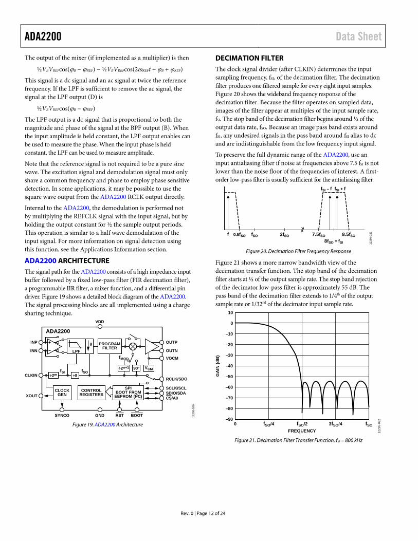
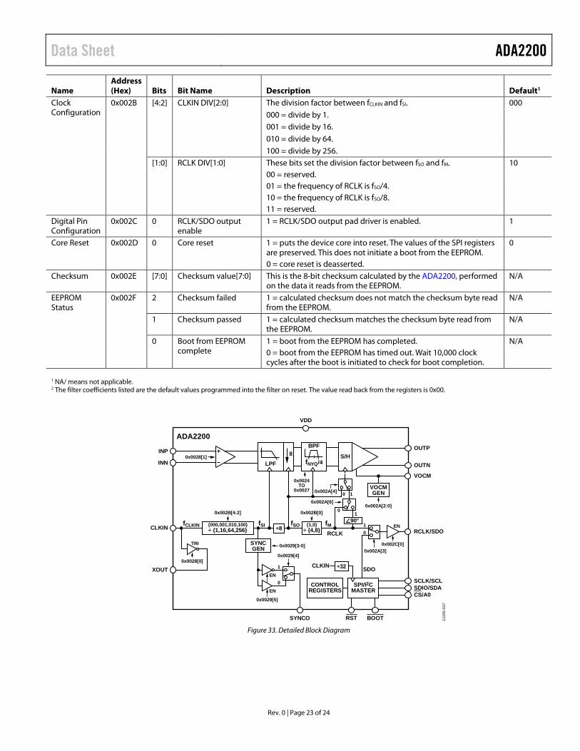
ADA2200 ARCHITECTURE The signal path for the ADA2200 consists of a high impedance input buffer followed by a fixed low-pass filter (FIR decimation filter), a programmable IIR filter, a mixer function, and a differential pin driver. Figure 19 shows a detailed block diagram of the ADA2200. The signal processing blocks are all implemented using a charge sharing technique.
Figure 19. ADA2200 Architecture
DECIMATION FILTER The clock signal divider (after CLKIN) determines the input sampling frequency, fSI, of the decimation filter. The decimation filter produces one filtered sample for every eight input samples. Figure 20 shows the wideband frequency response of the decimation filter. Because the filter operates on sampled data, images of the filter appear at multiples of the input sample rate, fSI. The stop band of the decimation filter begins around ½ of the output data rate, fSO. Because an image pass band exists around fSI, any undesired signals in the pass band around fSI alias to dc and are indistinguishable from the low frequency input signal.
To preserve the full dynamic range of the ADA2200, use an input antialiasing filter if noise at frequencies above 7.5 fSI is not lower than the noise floor of the frequencies of interest. A first-order low-pass filter is usually sufficient for the antialiasing filter.
Figure 20. Decimation Filter Frequency Response
Figure 21 shows a more narrow bandwidth view of the decimation transfer function. The stop band of the decimation filter starts at ½ of the output sample rate. The stop band rejection of the decimator low-pass filter is approximately 55 dB. The pass band of the decimation filter extends to 1/4th of the output sample rate or 1/32nd of the decimator input sample rate.
Figure 21. Decimation Filter Transfer Function, fSI = 800 kHz
INP
INN
OUTP
OUTN
VOCM
SCLK/SCLSDIO/SDACS/A0
RCLK/SDO
VDD
LPF
8 PROGRAMFILTER
CLOCKGEN
CONTROLREGISTERS
SPIBOOT FROM
EEPROM (I2C)
VCM÷2n+1
÷2m ÷890°fSOfSI
fMOD
XOUT
CLKIN
SYNCO GND RST BOOT
ADA2200
1229
5-02
0
0.5fSO fSO 2fSO 7.5fSO8fSO = fSI
fSI – f fSI + f
8.5fSOf
1229
5-02
1
GA
IN (d
B)
FREQUENCY
10
–10
–40
–70
–900 fSO/2 3fSO/4 fSO
–20
–30
–50
–60
0
–80
fSO/4
1229
5-02
2
Rev. 0 | Page 12 of 24
Data Sheet ADA2200
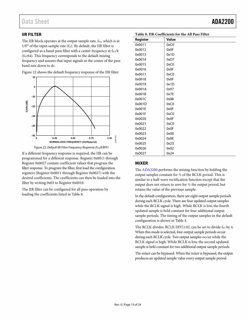
IIR FILTER The IIR block operates at the output sample rate, fSO, which is at 1/8th of the input sample rate (fSI). By default, the IIR filter is configured as a band-pass filter with a center frequency at fSO/8 (fSI/64). This frequency corresponds to the default mixing frequency and assures that input signals in the center of the pass band mix down to dc.
Figure 22 shows the default frequency response of the IIR filter.
Figure 22. Default IIR Filter Frequency Response (fSO/8 BPF)
If a different frequency response is required, the IIR can be programmed for a different response. Register 0x0011 through Register 0x0027 contain coefficient values that program the filter response. To program the filter, first load the configuration registers (Register 0x0011 through Register 0x0027) with the desired coefficients. The coefficients can then be loaded into the filter by writing 0x03 to Register 0x0010.
The IIR filter can be configured for all pass operation by loading the coefficients listed in Table 8.
Table 8. IIR Coefficients for the All Pass Filter Register Value 0x0011 0xC0 0x0012 0x0F 0x0013 0x1D 0x0014 0xD7 0x0015 0xC0 0x0016 0x0F 0x0017 0xC0 0x0018 0x0F 0x0019 0x1D 0x001A 0x97 0x001B 0x7E 0x001C 0x88 0x001D 0xC0 0x001E 0x0F 0x001F 0xC0 0x0020 0x0F 0x0021 0xC0 0x0022 0x0F 0x0023 0x00 0x0024 0x0E 0x0025 0x23 0x0026 0x02 0x0027 0x24
MIXER The ADA2200 performs the mixing function by holding the output samples constant for ½ of the RCLK period. This is similar to a half-wave rectification function except that the output does not return to zero for ½ the output period, but retains the value of the previous sample.
In the default configuration, there are eight output sample periods during each RCLK cycle. There are four updated output samples while the RCLK signal is high. While RCLK is low, the fourth updated sample is held constant for four additional output sample periods. The timing of the output samples in the default configuration is shown in Table 4.
The RCLK divider, RCLK DIV[1:0], can be set to divide fSO by 4. When this mode is selected, four output sample periods occur during each RCLK cycle. Two output samples occur while the RCLK signal is high. While RCLK is low, the second updated sample is held constant for two additional output sample periods.
The mixer can be bypassed. When the mixer is bypassed, the output produces an updated sample value every output sample period.
GA
IN (d
B)
NORMALIZED FREQUENCY (Hz/Nyquist)
10
–10
–40
–500 0.50 0.75 1.00
–20
–30
0
0.25
1229
5-02
3
Rev. 0 | Page 13 of 24
ADA2200 Data Sheet Phase Shifter
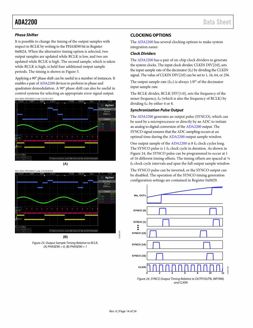
It is possible to change the timing of the output samples with respect to RCLK by writing to the PHASE90 bit in Register 0x002A. When the alternative timing option is selected, two output samples are updated while RCLK is low, and two are updated while RCLK is high. The second sample, which is taken while RCLK is high, is held four additional output sample periods. The timing is shown in Figure 5.
Applying a 90° phase shift can be useful in a number of instances. It enables a pair of ADA2200 devices to perform in phase and quadrature demodulation. A 90° phase shift can also be useful in control systems for selecting an appropriate error signal output.
Figure 23. Output Sample Timing Relative to RCLK,
(A) PHASE90 = 0, (B) PHASE90 = 1
CLOCKING OPTIONS The ADA2200 has several clocking options to make system integration easier.
Clock Dividers
The ADA2200 has a pair of on-chip clock dividers to generate the system clocks. The input clock divider, CLKIN DIV[2:0], sets the input sample rate of the decimator (fSI) by dividing the CLKIN signal. The value of CLKIN DIV[2:0] can be set to 1, 16, 64, or 256.
The output sample rate (fSO) is always 1/8th of the decimator input sample rate.
The RCLK divider, RCLK DIV[1:0], sets the frequency of the mixer frequency, fM (which is also the frequency of RCLK) by dividing fSO by either 4 or 8.
Synchronization Pulse Output
The ADA2200 generates an output pulse (SYNCO), which can be used by a microprocessor or directly by an ADC to initiate an analog to digital conversion of the ADA2200 output. The SYNCO signal ensures that the ADC sampling occurs at an optimal time during the ADA2200 output sample window.
One output sample of the ADA2200 is 8 fSI clock cycles long. The SYNCO pulse is 1 fSI clock cycle in duration. As shown in Figure 24, the SYNCO pulse can be programmed to occur at 1 of 16 different timing offsets. The timing offsets are spaced at ½ fSI clock cycle intervals and span the full output sample window.
The SYNCO pulse can be inverted, or the SYNCO output can be disabled. The operation of the SYNCO timing generation configuration settings are contained in Register 0x0029.
Figure 24. SYNCO Output Timing Relative to OUTP/OUTN, INP/INN,
and CLKIN
(A)
(B) 1229
5-02
4
INx, OUTx
SYNCO (0)
SYNCO (1)
SYNCO (13)
SYNCO (14)
SYNCO (15)
CLKIN
0 2 4 6 8 10 12 1229
5-02
5
Rev. 0 | Page 14 of 24
Data Sheet ADA2200
INPUT AND OUTPUT AMPLIFIERS Single-Ended Configurations
If a single-ended input configuration is desired, the input signal must have a common-mode voltage near midsupply. Decouple the other inputs to the common-mode voltage of the input signal.
Note that differences between the common-mode levels between the INP and INN inputs result in an offset voltage inside the device. Even though the BPF removes the offset, minimize the offset to avoid reducing the available signal swing internal to the device.
For single-ended outputs, either OUTP or OUTN can be used. Leave the unused output floating.
Differential Configurations
Using the ADA2200 in differential mode utilizes the full dynamic range of the device and provides the best noise performance and common-mode rejection.
Rev. 0 | Page 15 of 24
ADA2200 Data Sheet
APPLICATIONS INFORMATION The signal present at the output of the ADA2200 depends on the amplitude and relative phase of the signal applied at it inputs. When the amplitude or phase is known and constant, any output variations can be attributed to the modulated parameter. Therefore, when the relative phase of the input is constant, the ADA2200 performs amplitude demodulation. When the amplitude is constant, the ADA2200 performs phase demodulation.
The sampling and demodulation processes introduce additional frequency components onto the output signal. If the output signal of the ADA2200 is used in the analog domain or if it is sampled asynchronously to the ADA2200 sample clock, these high frequency components can be removed by following the ADA2200 with a reconstruction filter.
If the ADA2200 output is sampled synchronously to the ADA2200 output sample rate, an analog reconstruction filter is not required because the ADC inherently rejects sampling artifacts. The frequency artifacts introduced by the demodulation process can be removed by digital filtering.
AMPLITUDE MEASUREMENTS If the relative phase of the input signal to the ADA2200 remains constant, the output amplitude is directly proportional to the amplitude of the input signal. Note that the signal gain is a function of the relative phase of the input signal. Figure 15 shows the relationship between the cycle mean output and the relative phase. The cycle mean output voltage is
VCYCLEMEAN = Conversion Gain × VIN(RMS) × sin(θREL − θDEL) =
1.05 ×VIN(RMS) × sin(θREL − θDEL)
Therefore, the highest gain, and thus the largest signal-to-noise ratio measurement, is obtained when operating the ADA2200 with θREL = θDEL + 90° = 173°. This value of θREL is also the operating point with the lowest sensitivity to changes in the relative phase. Operating with θREL = θDEL − 90° = −7° offers the same gain and measurement accuracy, but with a sign inversion.
PHASE MEASUREMENTS If the amplitude of the input signal to the ADA2200 remains constant, the output amplitude is a function of the relative phase of the input signal. The relative phase can be measured as
θREL = sin−1(VCYCLEMEAN/(Conversion Gain × VIN(RMS))) + θDEL =
sin−1(VCYCLEMEAN/(1.05 × VIN(RMS))) + θDEL
Note that the output voltage scales directly with the input signal amplitude. A full-scale input signal provides the greatest phase sensitivity (V/°θREL) and thus the largest signal-to-noise ratio measurement.
The phase sensitivity also varies with relative phase. The sensitivity is at a maximum when θREL = 83°. For this reason, the optimal measurement range is for input signals with a relative phase equal to the phase delay of ±45°. This range provides the highest gain and thus the largest signal-to-noise ratio measurement. This range is also the operating point with the lowest sensitivity to changes in the relative phase. Operating at a relative phase equal to the phase delay of −135° to −225° offers the same gain and measurement accuracy, but with a sign inversion.
The phase sensitivity with a 4 V p-p differential input operating with a relative phase that is equal to the phase delay results in a phase sensitivity of 36.6 mV/°θREL.
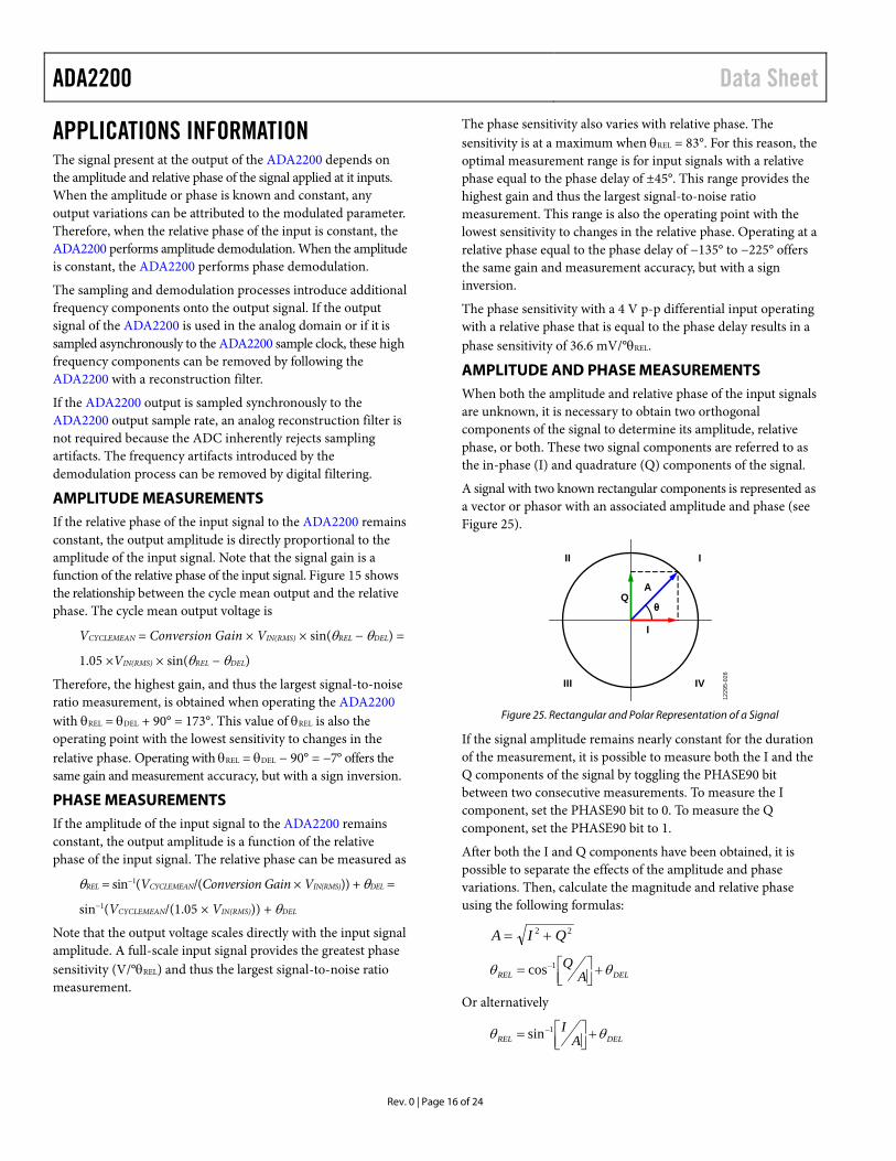
AMPLITUDE AND PHASE MEASUREMENTS When both the amplitude and relative phase of the input signals are unknown, it is necessary to obtain two orthogonal components of the signal to determine its amplitude, relative phase, or both. These two signal components are referred to as the in-phase (I) and quadrature (Q) components of the signal.
A signal with two known rectangular components is represented as a vector or phasor with an associated amplitude and phase (see Figure 25).
Figure 25. Rectangular and Polar Representation of a Signal
If the signal amplitude remains nearly constant for the duration of the measurement, it is possible to measure both the I and the Q components of the signal by toggling the PHASE90 bit between two consecutive measurements. To measure the I component, set the PHASE90 bit to 0. To measure the Q component, set the PHASE90 bit to 1.
After both the I and Q components have been obtained, it is possible to separate the effects of the amplitude and phase variations. Then, calculate the magnitude and relative phase using the following formulas:
22 QIA +=
DELREL AQ θθ +
= 1–cos
Or alternatively
DELREL AI θθ +
= 1–sin
QA
I
θ
III
IVIII
1229
5-02
6
Rev. 0 | Page 16 of 24
Data Sheet ADA2200 The inverse sine or inverse cosine functions linearize the relationship between the relative phase of the signal and the measured angle. Because the inverse sine and inverse cosine are only defined in two quadrants, the sign of I and Q must be considered to map the result over the entire 360° range of possible relative phase values. The use of the inverse tangent function is not recommended because the phase measurements become extremely sensitive to noise as the calculated phase approaches ±90°.
ANALOG OUTPUT SYSTEMS When the output signal of the ADA2200 is used in the analog domain or if it is sampled asynchronously to the ADA2200 sample clock, it is likely that a reconstruction filter is required.
Reconstruction Filters
The bandwidth of the analog reconstruction filter sets the demodulation bandwidth of the analog output. There is a direct trade-off between the noise and demodulation bandwidth. Therefore, it is recommended to ensure that the reconstruction filter cutoff frequency is as low as possible while minimizing the attenuation of the demodulated signal of interest.
Similar to a digital-to-analog converter (DAC), the output of the ADA2200 is a stepwise continuous output. This waveform contains positive and negative images of the desired signal at multiples of fSO. In most cases, the images are undesired noise components that must be attenuated.
The lowest frequency image to appear in the output spectrum appears at a frequency of fSO − fIN. The image amplitude is reduced by the sin(x)/x roll-off. System accuracy requirements may dictate that additional low-pass filtering is required to remove the output sample images.
INTERFACING TO ADCS Settling Time Considerations
If the ADC is coherently sampling the ADA2200 outputs, design the output filter to ensure that the output samples settle prior to ADC sampling. The output filter does not need to remove the sampling images generated by the ADA2200. The images are inherently rejected by the ADC sampling process.
Clock Synchronization
The SYNCO output can trigger the ADC sampling process directly, or a microcontroller can use SYNCO to adjust the ADC sampling time. Adjusting the SYNCO pulse timing can maximize the available time for the ADA2200 outputs to settle prior to ADC sampling.
Multichannel ADCs
In multichannel systems that require simultaneous sampling, the ADA2200 can provide per channel programmable filtering and simultaneous sampling.
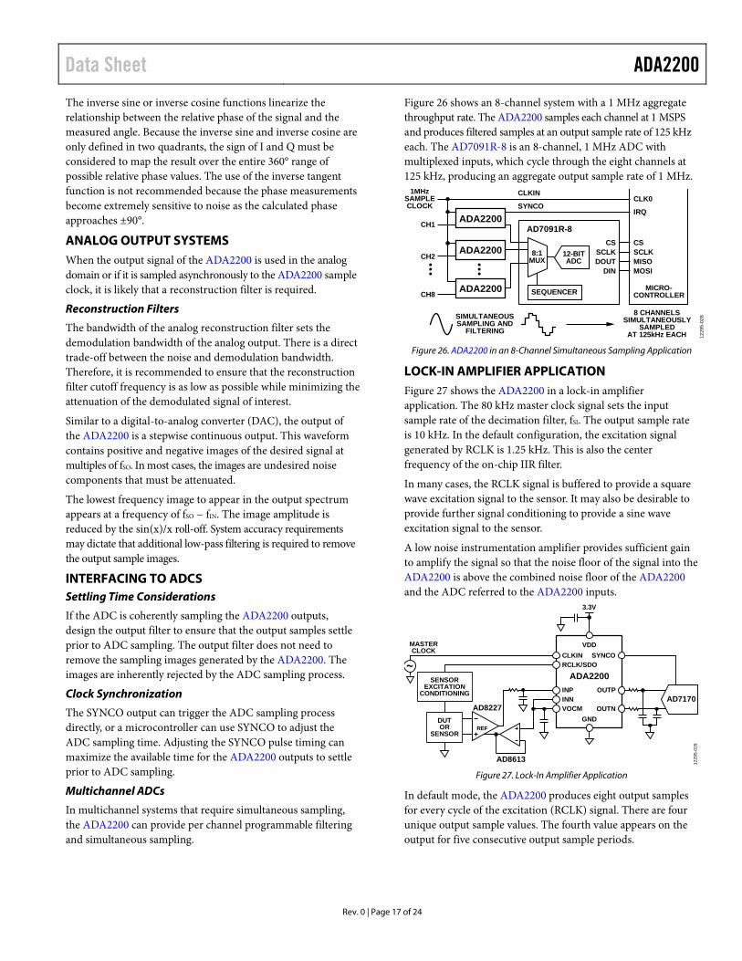
Figure 26 shows an 8-channel system with a 1 MHz aggregate throughput rate. The ADA2200 samples each channel at 1 MSPS and produces filtered samples at an output sample rate of 125 kHz each. The AD7091R-8 is an 8-channel, 1 MHz ADC with multiplexed inputs, which cycle through the eight channels at 125 kHz, producing an aggregate output sample rate of 1 MHz.
Figure 26. ADA2200 in an 8-Channel Simultaneous Sampling Application
LOCK-IN AMPLIFIER APPLICATION Figure 27 shows the ADA2200 in a lock-in amplifier application. The 80 kHz master clock signal sets the input sample rate of the decimation filter, fSI. The output sample rate is 10 kHz. In the default configuration, the excitation signal generated by RCLK is 1.25 kHz. This is also the center frequency of the on-chip IIR filter.
In many cases, the RCLK signal is buffered to provide a square wave excitation signal to the sensor. It may also be desirable to provide further signal conditioning to provide a sine wave excitation signal to the sensor.
A low noise instrumentation amplifier provides sufficient gain to amplify the signal so that the noise floor of the signal into the ADA2200 is above the combined noise floor of the ADA2200 and the ADC referred to the ADA2200 inputs.
Figure 27. Lock-In Amplifier Application
In default mode, the ADA2200 produces eight output samples for every cycle of the excitation (RCLK) signal. There are four unique output sample values. The fourth value appears on the output for five consecutive output sample periods.
SIMULTANEOUSSAMPLING AND
FILTERING
8 CHANNELSSIMULTANEOUSLY
SAMPLEDAT 125kHz EACH
MICRO-CONTROLLER
CH1
CH2
ADA2200SYNCO
ADA2200
CH8 ADA2200
12-BITADC
8:1MUX
SEQUENCER
AD7091R-8CS CS
IRQ
CLK0
SCLK SCLKDOUT MISO
DIN MOSI
CLKIN1MHzSAMPLECLOCK
1229
5-02
812
295-
029
CLKIN SYNCORCLK/SDO
INP OUTPINN
OUTNVOCM
VDD
GND
ADA2200SENSOREXCITATION
CONDITIONING
3.3V
DUTOR
SENSORREF
AD8227AD7170
MASTERCLOCK
AD8613
Rev. 0 | Page 17 of 24
ADA2200 Data Sheet There are several ways of digitally processing the output samples to optimize measurement accuracy, bandwidth, and throughput rate. One method is to take the sum of eight samples to return a value. A moving average filter lowers the noise floor of the returned values. The length of the moving average filter is determined by the noise floor and settling time requirements.
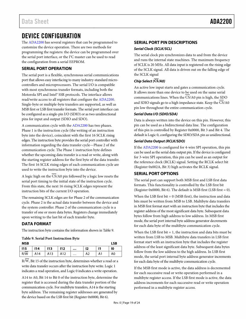
INTERFACING TO MICROCONTROLLERS The diagram in Figure 28 shows basic circuit configuration driven by a low power microcontroller (the ADuCM361). In this case, the ADA2200 reduces the ADC sampling rate by a factor of 8, and reduces the subsequent signal processing required by the microcontroller.
Figure 28. Fully Programmable Configuration:
Interface to Low Power Microcontroller
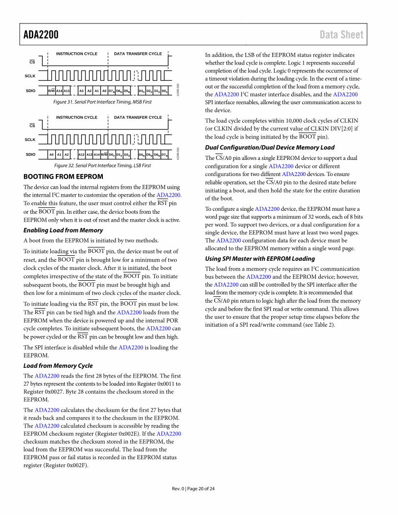
EEPROM BOOT CONFIGURATION The diagram in Figure 29 shows a standalone configuration with an EEPROM boot for the ADA2200. The standard oscillator circuit between CLKIN and XOUT generates the clock signal. Holding BOOT low during a power-on reset (POR) forces the ADA2200 to load its configuration from a preprogrammed EEPROM. An EEPROM boot is also initiated by bringing the BOOT pin low while the device in not in reset.
Figure 29. Standalone Configuration
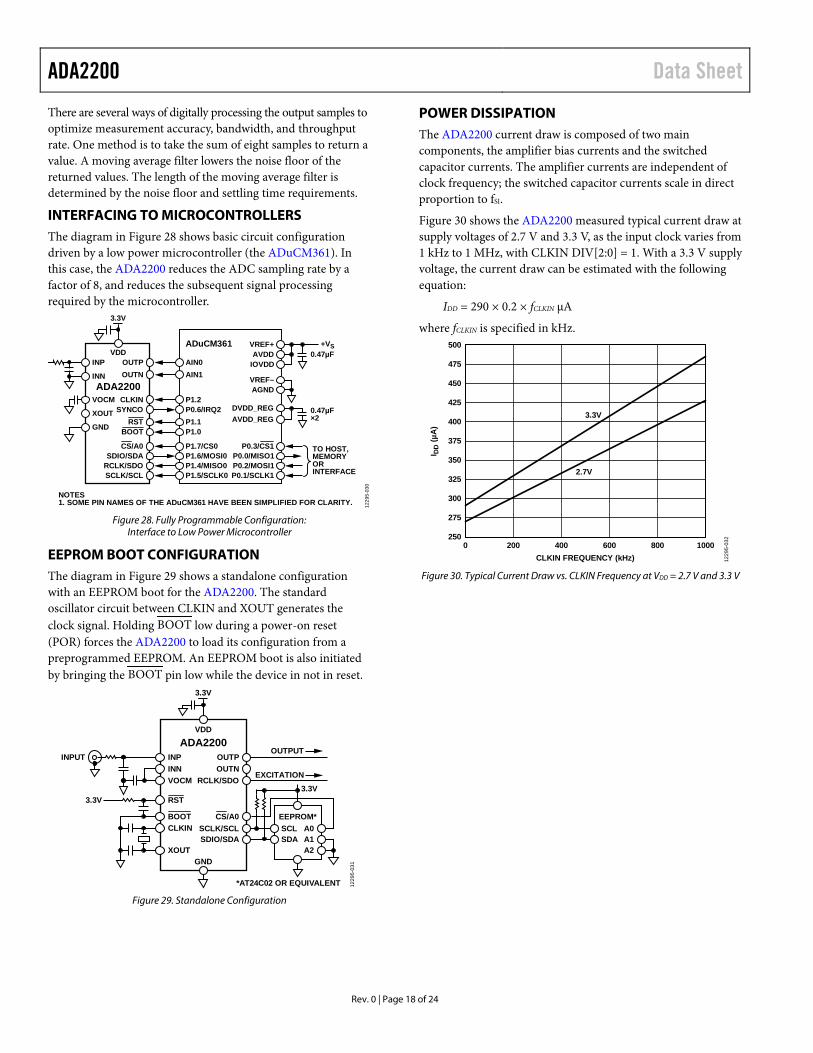
POWER DISSIPATION The ADA2200 current draw is composed of two main components, the amplifier bias currents and the switched capacitor currents. The amplifier currents are independent of clock frequency; the switched capacitor currents scale in direct proportion to fSI.
Figure 30 shows the ADA2200 measured typical current draw at supply voltages of 2.7 V and 3.3 V, as the input clock varies from 1 kHz to 1 MHz, with CLKIN DIV[2:0] = 1. With a 3.3 V supply voltage, the current draw can be estimated with the following equation:
IDD = 290 × 0.2 × fCLKIN µA
where fCLKIN is specified in kHz.
Figure 30. Typical Current Draw vs. CLKIN Frequency at VDD = 2.7 V and 3.3 V
INP OUTPOUTN
CLKINSYNCO
RSTBOOT
CS/A0SDIO/SDA
RCLK/SDOSCLK/SCL
AIN0AIN1
P1.2P0.6/IRQ2P1.1P1.0
P1.7/CS0P1.6/MOSI0P1.4/MISO0P1.5/SCLK0
P0.3/CS1
AVDD_REGDVDD_REG
AGNDVREF–
IOVDDAVDD
VREF+
P0.0/MISO1P0.2/MOSI1P0.1/SCLK1
VOCM
XOUT
GND
VDD
ADA2200
3.3V
INN
TO HOST,MEMORYORINTERFACE
0.47µF×2
0.47µF+VSADuCM361
1229
5-03
0
NOTES1. SOME PIN NAMES OF THE ADuCM361 HAVE BEEN SIMPLIFIED FOR CLARITY.
VDD
ADA2200
3.3V
SCL A0SDA
SCLK/SCLSDIO/SDA
CS/A0
A1A2
EEPROM*
*AT24C02 OR EQUIVALENT
3.3VRCLK/SDO
OUTNOUTP
VOCMINN
RST
BOOTCLKIN
XOUT
INPOUTPUT
EXCITATION
INPUT
GND
3.3V
1229
5-03
1500
250
275
300
325
350
375
400
425
450
475
0 1000800600400200
I DD
(µA
)
CLKIN FREQUENCY (kHz)
2.7V
3.3V
1229
5-03
2
Rev. 0 | Page 18 of 24
Data Sheet ADA2200
DEVICE CONFIGURATION The ADA2200 has several registers that can be programmed to customize the device operation. There are two methods for programming the registers: the device can be programmed over the serial port interface, or the I2C master can be used to read the configuration from a serial EEPROM.
SERIAL PORT OPERATION The serial port is a flexible, synchronous serial communications port that allows easy interfacing to many industry-standard micro-controllers and microprocessors. The serial I/O is compatible with most synchronous transfer formats, including both the Motorola SPI and Intel® SSR protocols. The interface allows read/write access to all registers that configure the ADA2200. Single-byte or multiple-byte transfers are supported, as well as MSB first or LSB first transfer formats. The serial port interface can be configured as a single-pin I/O (SDIO) or as two unidirectional pins for input and output (SDIO and SDO).
A communication cycle with the ADA2200 has two phases. Phase 1 is the instruction cycle (the writing of an instruction byte into the device), coincident with the first 16 SCLK rising edges. The instruction byte provides the serial port controller with information regarding the data transfer cycle—Phase 2 of the communication cycle. The Phase 1 instruction byte defines whether the upcoming data transfer is a read or write, along with the starting register address for the first byte of the data transfer. The first 16 SCLK rising edges of each communication cycle are used to write the instruction byte into the device.
A logic high on the CS/A0 pin followed by a logic low resets the serial port timing to the initial state of the instruction cycle. From this state, the next 16 rising SCLK edges represent the instruction bits of the current I/O operation.
The remaining SCLK edges are for Phase 2 of the communication cycle. Phase 2 is the actual data transfer between the device and the system controller. Phase 2 of the communication cycle is a transfer of one or more data bytes. Registers change immediately upon writing to the last bit of each transfer byte.
DATA FORMAT The instruction byte contains the information shown in Table 9.
Table 9. Serial Port Instruction Byte MSB LSB I15 I14 I13 I12 … I2 I1 I0 R/W A14 A13 A12 … A2 A1 A0
R/W, Bit 15 of the instruction byte, determines whether a read or a write data transfer occurs after the instruction byte write. Logic 1 indicates a read operation, and Logic 0 indicates a write operation.
A14 to A0, Bit 14 to Bit 0 of the instruction byte, determine the register that is accessed during the data transfer portion of the communication cycle. For multibyte transfers, A14 is the starting byte address. The remaining register addresses are generated by the device based on the LSB first bit (Register 0x0000, Bit 6).
SERIAL PORT PIN DESCRIPTIONS Serial Clock (SCLK/SCL)
The serial clock pin synchronizes data to and from the device and runs the internal state machines. The maximum frequency of SCLK is 20 MHz. All data input is registered on the rising edge of the SCLK signal. All data is driven out on the falling edge of the SCLK signal
Chip Select (CS/A0)
An active low input starts and gates a communication cycle. It allows more than one device to be used on the same serial communications lines. When the CS/A0 pin is high, the SDO and SDIO signals go to a high impedance state. Keep the CS/A0 pin low throughout the entire communication cycle.
Serial Data I/O (SDIO/SDA)
Data is always written into the device on this pin. However, this pin can be used as a bidirectional data line. The configuration of this pin is controlled by Register 0x0000, Bit 3 and Bit 4. The default is Logic 0, configuring the SDIO/SDA pin as unidirectional.
Serial Data Output (RCLK/SDO)
If the ADA2200 is configured for 4-wire SPI operation, this pin can be used as the serial data output pin. If the device is configured for 3-wire SPI operation, this pin can be used as an output for the reference clock (RCLK) signal. Setting the RCLK select bit (Register 0x002A, Bit 3) high activates the RCLK signal.
SERIAL PORT OPTIONS The serial port can support both MSB first and LSB first data formats. This functionality is controlled by the LSB first bit (Register 0x0000, Bit 6). The default is MSB first (LSB first = 0).
When the LSB first bit = 0 (MSB first), the instruction and data bits must be written from MSB to LSB. Multibyte data transfers in MSB first format start with an instruction byte that includes the register address of the most significant data byte. Subsequent data bytes follow from high address to low address. In MSB first mode, the serial port internal byte address generator decrements for each data byte of the multibyte communication cycle.
When the LSB first bit = 1, the instruction and data bits must be written from LSB to MSB. Multibyte data transfers in LSB first format start with an instruction byte that includes the register address of the least significant data byte. Subsequent data bytes follow from the low address to the high address. In LSB first mode, the serial port internal byte address generator increments for each data byte of the multibyte communication cycle.
If the MSB first mode is active, the data address is decremented for each successive read or write operation performed in a multibyte register access. If the LSB first mode is active, the data address increments for each successive read or write operation performed in a multibyte register access.
Rev. 0 | Page 19 of 24
ADA2200 Data Sheet
Figure 31. Serial Port Interface Timing, MSB First
Figure 32. Serial Port Interface Timing, LSB First
BOOTING FROM EEPROM The device can load the internal registers from the EEPROM using the internal I2C master to customize the operation of the ADA2200. To enable this feature, the user must control either the RST pin or the BOOT pin. In either case, the device boots from the EEPROM only when it is out of reset and the master clock is active.
Enabling Load from Memory
A boot from the EEPROM is initiated by two methods.
To initiate loading via the BOOT pin, the device must be out of reset, and the BOOT pin is brought low for a minimum of two clock cycles of the master clock. After it is initiated, the boot completes irrespective of the state of the BOOT pin. To initiate subsequent boots, the BOOT pin must be brought high and then low for a minimum of two clock cycles of the master clock.
To initiate loading via the RST pin, the BOOT pin must be low. The RST pin can be tied high and the ADA2200 loads from the EEPROM when the device is powered up and the internal POR cycle completes. To initiate subsequent boots, the ADA2200 can be power cycled or the RST pin can be brought low and then high.
The SPI interface is disabled while the ADA2200 is loading the EEPROM.
Load from Memory Cycle
The ADA2200 reads the first 28 bytes of the EEPROM. The first 27 bytes represent the contents to be loaded into Register 0x0011 to Register 0x0027. Byte 28 contains the checksum stored in the EEPROM.
The ADA2200 calculates the checksum for the first 27 bytes that it reads back and compares it to the checksum in the EEPROM. The ADA2200 calculated checksum is accessible by reading the EEPROM checksum register (Register 0x002E). If the ADA2200 checksum matches the checksum stored in the EEPROM, the load from the EEPROM was successful. The load from the EEPROM pass or fail status is recorded in the EEPROM status register (Register 0x002F).
In addition, the LSB of the EEPROM status register indicates whether the load cycle is complete. Logic 1 represents successful completion of the load cycle. Logic 0 represents the occurrence of a timeout violation during the loading cycle. In the event of a time-out or the successful completion of the load from a memory cycle, the ADA2200 I2C master interface disables, and the ADA2200 SPI interface reenables, allowing the user communication access to the device.
The load cycle completes within 10,000 clock cycles of CLKIN (or CLKIN divided by the current value of CLKIN DIV[2:0] if the load cycle is being initiated by the BOOT pin).
Dual Configuration/Dual Device Memory Load
The CS/A0 pin allows a single EEPROM device to support a dual configuration for a single ADA2200 device or different configurations for two different ADA2200 devices. To ensure reliable operation, set the CS/A0 pin to the desired state before initiating a boot, and then hold the state for the entire duration of the boot.
To configure a single ADA2200 device, the EEPROM must have a word page size that supports a minimum of 32 words, each of 8 bits per word. To support two devices, or a dual configuration for a single device, the EEPROM must have at least two word pages. The ADA2200 configuration data for each device must be allocated to the EEPROM memory within a single word page.
Using SPI Master with EEPROM Loading
The load from a memory cycle requires an I2C communication bus between the ADA2200 and the EEPROM device; however, the ADA2200 can still be controlled by the SPI interface after the load from the memory cycle is complete. It is recommended that the CS/A0 pin return to logic high after the load from the memory cycle and before the first SPI read or write command. This allows the user to ensure that the proper setup time elapses before the initiation of a SPI read/write command (see Table 2).
R/W A14 A13 A3 A2 A1 A0 D7N D6N D5N D00D10D20D30
INSTRUCTION CYCLE DATA TRANSFER CYCLE
SCLK
SDIO
CS
1229
5-03
3
A0 A1 A2 A12 A13 A14 D00 D10 D20 D7ND6ND5ND4N
INSTRUCTION CYCLE DATA TRANSFER CYCLE
SCLK
SDIO
CS
R/W
1229
5-03
4
Rev. 0 | Page 20 of 24
Data Sheet ADA2200
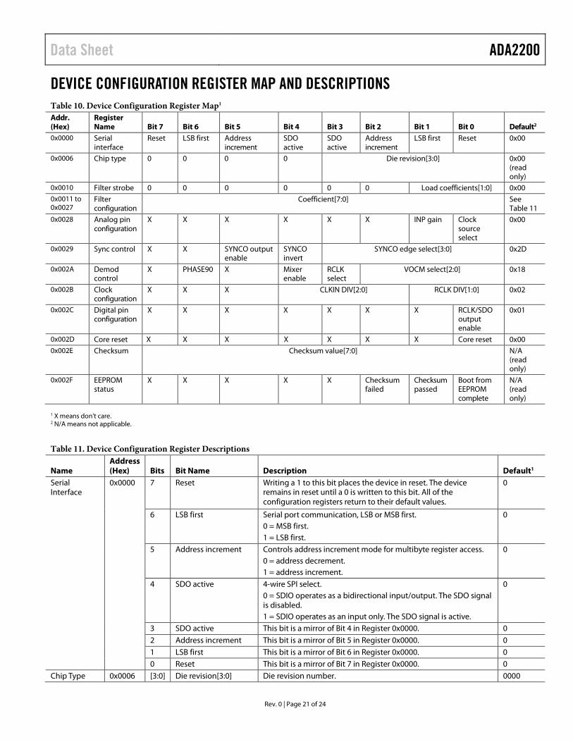
DEVICE CONFIGURATION REGISTER MAP AND DESCRIPTIONS Table 10. Device Configuration Register Map1 Addr. (Hex)
Register Name Bit 7 Bit 6 Bit 5 Bit 4 Bit 3 Bit 2 Bit 1 Bit 0 Default2
0x0000 Serial interface
Reset LSB first Address increment
SDO active
SDO active
Address increment
LSB first Reset 0x00
0x0006 Chip type 0 0 0 0 Die revision[3:0] 0x00 (read only)
0x0010 Filter strobe 0 0 0 0 0 0 Load coefficients[1:0] 0x00 0x0011 to 0x0027
Filter configuration
Coefficient[7:0] See Table 11
0x0028 Analog pin configuration
X X X X X X INP gain Clock source select
0x00
0x0029 Sync control X X SYNCO output enable
SYNCO invert
SYNCO edge select[3:0] 0x2D
0x002A Demod control
X PHASE90 X Mixer enable
RCLK select
VOCM select[2:0] 0x18
0x002B Clock configuration
X X X CLKIN DIV[2:0] RCLK DIV[1:0] 0x02
0x002C Digital pin configuration
X X X X X X X RCLK/SDO output enable
0x01
0x002D Core reset X X X X X X X Core reset 0x00 0x002E Checksum Checksum value[7:0] N/A
(read only)
0x002F EEPROM status
X X X X X Checksum failed
Checksum passed
Boot from EEPROM complete
N/A (read only)
1 X means don’t care. 2 N/A means not applicable.
Table 11. Device Configuration Register Descriptions
Name Address (Hex) Bits Bit Name Description Default1
Serial Interface
0x0000 7 Reset Writing a 1 to this bit places the device in reset. The device remains in reset until a 0 is written to this bit. All of the configuration registers return to their default values.
0
6 LSB first Serial port communication, LSB or MSB first. 0 0 = MSB first. 1 = LSB first.
5 Address increment Controls address increment mode for multibyte register access. 0 0 = address decrement. 1 = address increment. 4 SDO active 4-wire SPI select. 0
0 = SDIO operates as a bidirectional input/output. The SDO signal is disabled.
1 = SDIO operates as an input only. The SDO signal is active. 3 SDO active This bit is a mirror of Bit 4 in Register 0x0000. 0 2 Address increment This bit is a mirror of Bit 5 in Register 0x0000. 0 1 LSB first This bit is a mirror of Bit 6 in Register 0x0000. 0 0 Reset This bit is a mirror of Bit 7 in Register 0x0000. 0 Chip Type 0x0006 [3:0] Die revision[3:0] Die revision number. 0000
Rev. 0 | Page 21 of 24
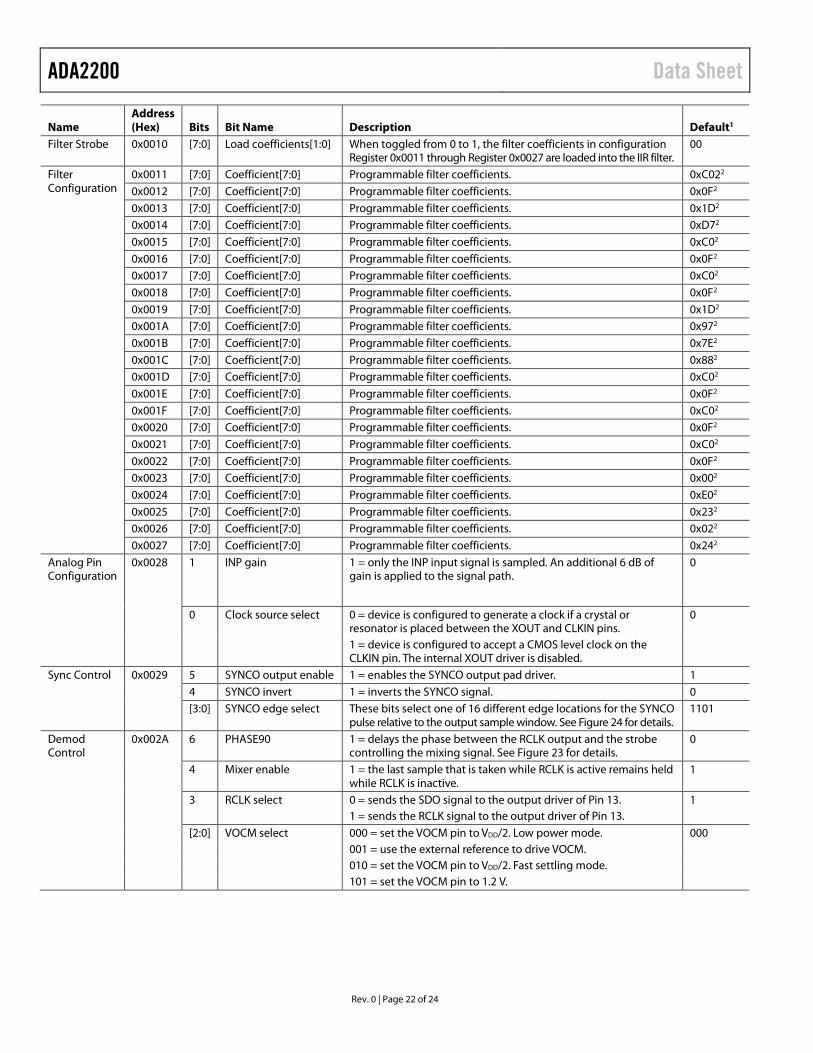
ADA2200 Data Sheet
Name Address (Hex) Bits Bit Name Description Default1
Filter Strobe 0x0010 [7:0] Load coefficients[1:0] When toggled from 0 to 1, the filter coefficients in configuration Register 0x0011 through Register 0x0027 are loaded into the IIR filter.
00
Filter Configuration
0x0011 [7:0] Coefficient[7:0] Programmable filter coefficients. 0xC022 0x0012 [7:0] Coefficient[7:0] Programmable filter coefficients. 0x0F2 0x0013 [7:0] Coefficient[7:0] Programmable filter coefficients. 0x1D2 0x0014 [7:0] Coefficient[7:0] Programmable filter coefficients. 0xD72 0x0015 [7:0] Coefficient[7:0] Programmable filter coefficients. 0xC02 0x0016 [7:0] Coefficient[7:0] Programmable filter coefficients. 0x0F2 0x0017 [7:0] Coefficient[7:0] Programmable filter coefficients. 0xC02 0x0018 [7:0] Coefficient[7:0] Programmable filter coefficients. 0x0F2 0x0019 [7:0] Coefficient[7:0] Programmable filter coefficients. 0x1D2 0x001A [7:0] Coefficient[7:0] Programmable filter coefficients. 0x972 0x001B [7:0] Coefficient[7:0] Programmable filter coefficients. 0x7E2 0x001C [7:0] Coefficient[7:0] Programmable filter coefficients. 0x882 0x001D [7:0] Coefficient[7:0] Programmable filter coefficients. 0xC02 0x001E [7:0] Coefficient[7:0] Programmable filter coefficients. 0x0F2 0x001F [7:0] Coefficient[7:0] Programmable filter coefficients. 0xC02 0x0020 [7:0] Coefficient[7:0] Programmable filter coefficients. 0x0F2 0x0021 [7:0] Coefficient[7:0] Programmable filter coefficients. 0xC02 0x0022 [7:0] Coefficient[7:0] Programmable filter coefficients. 0x0F2 0x0023 [7:0] Coefficient[7:0] Programmable filter coefficients. 0x002 0x0024 [7:0] Coefficient[7:0] Programmable filter coefficients. 0xE02 0x0025 [7:0] Coefficient[7:0] Programmable filter coefficients. 0x232 0x0026 [7:0] Coefficient[7:0] Programmable filter coefficients. 0x022 0x0027 [7:0] Coefficient[7:0] Programmable filter coefficients. 0x242
Analog Pin Configuration
0x0028 1 INP gain 1 = only the INP input signal is sampled. An additional 6 dB of gain is applied to the signal path.
0
0 Clock source select 0 = device is configured to generate a clock if a crystal or resonator is placed between the XOUT and CLKIN pins.
0
1 = device is configured to accept a CMOS level clock on the CLKIN pin. The internal XOUT driver is disabled.
Sync Control 0x0029 5 SYNCO output enable 1 = enables the SYNCO output pad driver. 1 4 SYNCO invert 1 = inverts the SYNCO signal. 0
[3:0] SYNCO edge select These bits select one of 16 different edge locations for the SYNCO
pulse relative to the output sample window. See Figure 24 for details. 1101
Demod Control
0x002A 6 PHASE90 1 = delays the phase between the RCLK output and the strobe controlling the mixing signal. See Figure 23 for details.
0
4 Mixer enable 1 = the last sample that is taken while RCLK is active remains held while RCLK is inactive.
1
3 RCLK select 0 = sends the SDO signal to the output driver of Pin 13. 1 1 = sends the RCLK signal to the output driver of Pin 13. [2:0] VOCM select 000 = set the VOCM pin to VDD/2. Low power mode. 000
001 = use the external reference to drive VOCM. 010 = set the VOCM pin to VDD/2. Fast settling mode. 101 = set the VOCM pin to 1.2 V.
Rev. 0 | Page 22 of 24
Data Sheet ADA2200
Name Address (Hex) Bits Bit Name Description Default1
Clock Configuration
0x002B [4:2] CLKIN DIV[2:0] The division factor between fCLKIN and fSI. 000 000 = divide by 1. 001 = divide by 16. 010 = divide by 64. 100 = divide by 256. [1:0] RCLK DIV[1:0] These bits set the division factor between fSO and fM. 10
00 = reserved. 01 = the frequency of RCLK is fSO/4. 10 = the frequency of RCLK is fSO/8. 11 = reserved. Digital Pin Configuration
0x002C 0 RCLK/SDO output enable
1 = RCLK/SDO output pad driver is enabled. 1
Core Reset 0x002D 0 Core reset 1 = puts the device core into reset. The values of the SPI registers are preserved. This does not initiate a boot from the EEPROM.
0
0 = core reset is deasserted. Checksum 0x002E [7:0] Checksum value[7:0] This is the 8-bit checksum calculated by the ADA2200, performed
on the data it reads from the EEPROM. N/A
EEPROM Status
0x002F 2 Checksum failed 1 = calculated checksum does not match the checksum byte read from the EEPROM.
N/A
1 Checksum passed 1 = calculated checksum matches the checksum byte read from the EEPROM.
N/A
0 Boot from EEPROM complete
1 = boot from the EEPROM has completed. N/A 0 = boot from the EEPROM has timed out. Wait 10,000 clock
cycles after the boot is initiated to check for boot completion.
1 NA/ means not applicable. 2 The filter coefficients listed are the default values programmed into the filter on reset. The value read back from the registers is 0x00.
Figure 33. Detailed Block Diagram
10
1
0
INP
INN
CLKIN
XOUT
VOCM
RCLK/SDO
OUTN
OUTP
VDD
LPF
8
÷8
SYNCO
SCLK/SCLSDIO/SDACS/A0
CONTROLREGISTERS
SPI/I2CMASTER
RST BOOT
ADA2200
0x0028[1]
0x0024TO
0x0027 0x002A[4]
0x002A[6]
{000,001,010,100}÷ {1,16,64,256}
fSO fMfSIfCLKIN
0x002B[4:2]
{1,0}÷ {4,8}
0x002B[0]
BPF
fNYQ/4S/H
VOCMGEN
0x002A[2:0]
0x002A[3]0x002C[0]0x0029[3:0]
0x0029[5]
0x0029[4]0x0028[0]
90°
0 1
01
ENRCLK
TRI SYNCGEN
EN
EN
÷32CLKIN SDO
1229
5-03
7
Rev. 0 | Page 23 of 24
ADA2200 Data Sheet
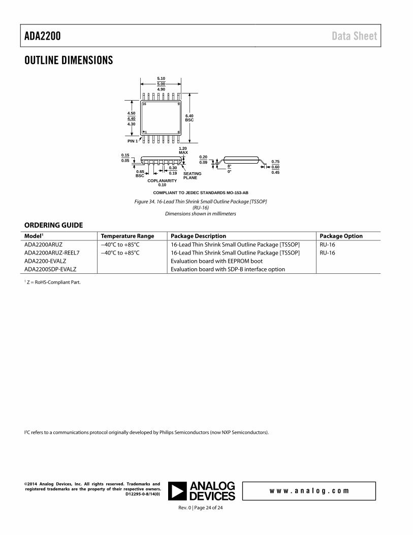
OUTLINE DIMENSIONS
Figure 34. 16-Lead Thin Shrink Small Outline Package [TSSOP]
(RU-16) Dimensions shown in millimeters
ORDERING GUIDE Model1 Temperature Range Package Description Package Option ADA2200ARUZ −40°C to +85°C 16-Lead Thin Shrink Small Outline Package [TSSOP] RU-16 ADA2200ARUZ-REEL7 −40°C to +85°C 16-Lead Thin Shrink Small Outline Package [TSSOP] RU-16 ADA2200-EVALZ Evaluation board with EEPROM boot ADA2200SDP-EVALZ Evaluation board with SDP-B interface option
1 Z = RoHS-Compliant Part.
I2C refers to a communications protocol originally developed by Philips Semiconductors (now NXP Semiconductors).
16 9
81
PIN 1
SEATINGPLANE
8°0°
4.504.404.30
6.40BSC
5.105.004.90
0.65BSC
0.150.05
1.20MAX
0.200.09 0.75
0.600.45
0.300.19
COPLANARITY0.10
COMPLIANT TO JEDEC STANDARDS MO-153-AB
©2014 Analog Devices, Inc. All rights reserved. Trademarks and registered trademarks are the property of their respective owners. D12295-0-8/14(0)
Rev. 0 | Page 24 of 24