Embed Size (px)
Citation preview
Symmetric Key Cryptography onModern Graphics Hardware
Jason Yang and James Goodman
Advanced Micro Devices, Inc.Graphics Product Group
{jasonc.yang,jim.goodman}@amd.com
Abstract. GPUs offer a tremendous amount of computational band-width that was until now largely unusable for cryptographic computa-tions due to a lack of integer arithmetic and user-friendly programmingAPIs that provided direct access to the GPU’s computing resources. Thelatest generation of GPUs, which introduces integer/binary arithmetic,has been leveraged to create several implementations of the AES andDES symmetric key algorithms. Both conventional and bitsliced imple-mentations are described that achieve data rates on the order of 3-30Gbps from a single AMD HD 2900 XT graphics card, yielding speedupsof 6-60x over equivalent implementations on high-performance CPUs.
1 Introduction
In recent years, there has been significant interest from both academia and in-dustry in applying commodity graphics processing units (GPUs) toward gen-eral computing problems [1]. This trend toward general-purpose computationon GPUs (GPGPU) is spurred by the large number of arithmetic units andthe high memory bandwidth available in today’s GPUs. In certain applications,where there is a high compute to memory bandwidth ratio (a.k.a., arithmeticintensity) the GPU has the potential to be orders of magnitude faster than con-ventional CPUs due to the parallel nature of GPUs versus CPUs, which areinherently optimized for sequential code. In addition, the computational powerof GPUs is growing at a faster rate than what Moore’s Law predicts for CPUs(Figure 1).
With the introduction of native integer and binary operations in the latestgeneration of GPUs, we believe that bulk encryption and its related applications(e.g., key searching) are ideally suited to the GPGPU programming model. Inthis paper we demonstrate the viability of the GPGPU programming modelfor implementing symmetric key ciphers on GPUs. We examine high-efficiencybitsliced implementations of the AES and DES algorithms, as well as compareconventional block-based implementations of AES on previous/current genera-tion GPUs. We demonstrate AES and DES running on an AMD HD 2900 XTGPU to be up to 16 and 60 times faster respectively than high end CPUs.
The following section describes previous work related to implementing sym-metric cryptographic algorithms on GPUs and vector-based processors. Next we
Pe
rfo
rma
nc
e (
GF
LO
PS
)
CPU
GPU250
300
200
100
150
50
0
1998 1999 2000 2001 2002 2003 2004 2005 2006
Fig. 1. GPU vs. CPU GFLOPS performance over time
describe GPU hardware architecture and programming APIs to provide contextfor the GPGPU programming model. Bitsliced implementations of DES andAES are then described in the context of high-performance GPGPU-acceleratedkey searching applications that demonstrate the potential speedup of GPUs overconventional CPUs in certain classes of problems. Lastly, a comparison of a con-ventional block-based implementation of AES on both the current and previousgenerations of GPUs is presented to illustrate the computational advantages ofthe latest generation of GPUs.
2 Previous Work
Cook et al. [2] were the first to investigate the feasibility of using GPUs forsymmetric key encryption. Using OpenGL they implemented AES on variousprevious-generation GPUs. Unfortunately, the limited capability of the graphicsprogramming model they used limited their performance and prevented themfrom exploiting some of the programmable features of their hardware. Insteadthey were forced to use a fixed-function pipeline, rely on color maps to transformbytes, and exploit a hardware XOR unit in the output-merger stage. A completeexecution of AES required multiple passes through the pipeline, which signifi-cantly impacted their performance. Their experiments found that the GPU couldonly perform at about 2.3% of the CPU rate when both were running code op-
timized for their individual instruction sets. A recent OpenGL implementation[3] on a NVIDIA Geforce 8800 GTS achieves rates of almost 3 Gbps.
Vector processors have been considered for implementation of symmetric al-gorithms such as DES [4], and cryptography in general [5], which yielded someperformance increase. Recently, Costigan and Scott [6] implemented RSA usingthe vector units of the Cell processor. They were able to achieve rates up to 7×faster using 6 vector units (SPU) over the onboard PowerPC unit (PPU).
3 GPGPU Programming Model
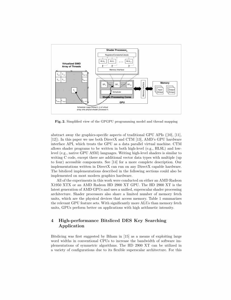
The latest generation of GPUs (e.g., Nvidia’s 8000 series or AMD’s HD 2000series) has adopted the unified shader programming model pioneered by AMDin the Xbox 360’s GPU [7]. In the unified shader model, all graphics functionsare executed on programmable ALUs that can handle the different types of pro-grams (i.e., shader programs) that need to be run by the different stages ofthe conventional graphics pipeline. The programmable nature of these ALUscan be exploited to implement non-graphics functions using a virtualized SIMDprocessing programming model that operates on streams of data. In this pro-gramming model, arrays of input data elements stored in memory are mappedone-to-one onto the virtualized SIMD array, which executes a shader programto generate one or more outputs that are then written back to output arraysin memory. Each instance of a shader program running on a virtualized SIMDarray element is called a thread. The GPU and its components map the array ofthreads onto a finite pool of physical shader processors (SPs) by scheduling theavailable resources in the GPU such that each element of the virtual SIMD arrayis eventually processed, at which point additional shader programs can also beexecuted until the application has completed. A simplified view of the GPGPUprogramming model and mapping of threads to the GPUs processing resourcesis shown in Figure 2.
Modern GPUs are designed to be very efficient at running large numbers ofthreads (e.g., thousands/millions) in a manner that is transparent to the appli-cation/user. The GPU uses the large number of threads to hide memory accesslatencies by having the resource scheduler switch the active thread in a givenSP whenever the current thread finds itself stalled waiting for a memory accessto complete. Time multiplexing is also used in the SPs’ ALUs to execute multi-ple threads concurrently and hide the latency of ALU operations via pipelining.Both of these techniques require that a thread contains a large number of calcula-tions to improve the ability of the resource scheduler to hide the aforementionedlatencies. When that condition is satisfied, the entire computational bandwidthof the GPU can be utilized to help GPGPU applications achieve performanceincreases on the order of 10− 100× over conventional CPUs.
DirectX [8] and OpenGL [9] are the standard programming APIs for GPUsand provide high-level languages for writing shader programs (e.g., HLSL andGLSL). However, these APIs are optimized for graphics and are difficult to usefor non-graphics developers. Recently several projects have begun to try and
Memory
GPU
Shader Processing Cores
SP0 SPk. . . SPN-1
Scheduler
. . .
Memory Interface
T0,0 TNx-1,0
TNx-1,1
T1,0
T0,1 T1,1
T0,Ny-1 T1,Ny-1 TNx-1,Ny-1
Ti,j...
...
...
Virtualized SIMD
Array of Threads
Scheduler maps thread (i, j) of virtual
array onto phyical shader processor k
Input
Arrays
Output
Arrays
...
...
...
Shader Processork
ALU0
Registers/Constants/Literals
Memory Interface
. . .ALU1 ALUn-1
......
...
...
Ny
Nx
Fig. 2. Simplified view of the GPGPU programming model and thread mapping
abstract away the graphics-specific aspects of traditional GPU APIs ([10], [11],[12]). In this paper we use both DirectX and CTM [13], AMD’s GPU hardwareinterface API, which treats the GPU as a data parallel virtual machine. CTMallows shader programs to be written in both high-level (e.g., HLSL) and low-level (e.g., native GPU ASM) languages. Writing high-level shaders is similar towriting C code, except there are additional vector data types with multiple (upto four) accessible components. See [14] for a more complete description. Ourimplementations written in DirectX can run on any DirectX capable hardware.The bitsliced implementations described in the following sections could also beimplemented on most modern graphics hardware.
All of the experiments in this work were conducted on either an AMD RadeonX1950 XTX or an AMD Radeon HD 2900 XT GPU. The HD 2900 XT is thelatest generation of AMD GPUs and uses a unified, superscalar shader processingarchitecture. Shader processors also share a limited number of memory fetchunits, which are the physical devices that access memory. Table 1 summarizesthe relevant GPU feature sets. With significantly more ALUs than memory fetchunits, GPUs perform better on applications with high arithmetic intensity.
4 High-performance Bitsliced DES Key SearchingApplication
Bitslicing was first suggested by Biham in [15] as a means of exploiting largeword widths in conventional CPUs to increase the bandwidth of software im-plementations of symmetric algorithms. The HD 2900 XT can be utilized ina variety of configurations due to its flexible superscalar architecture. For this
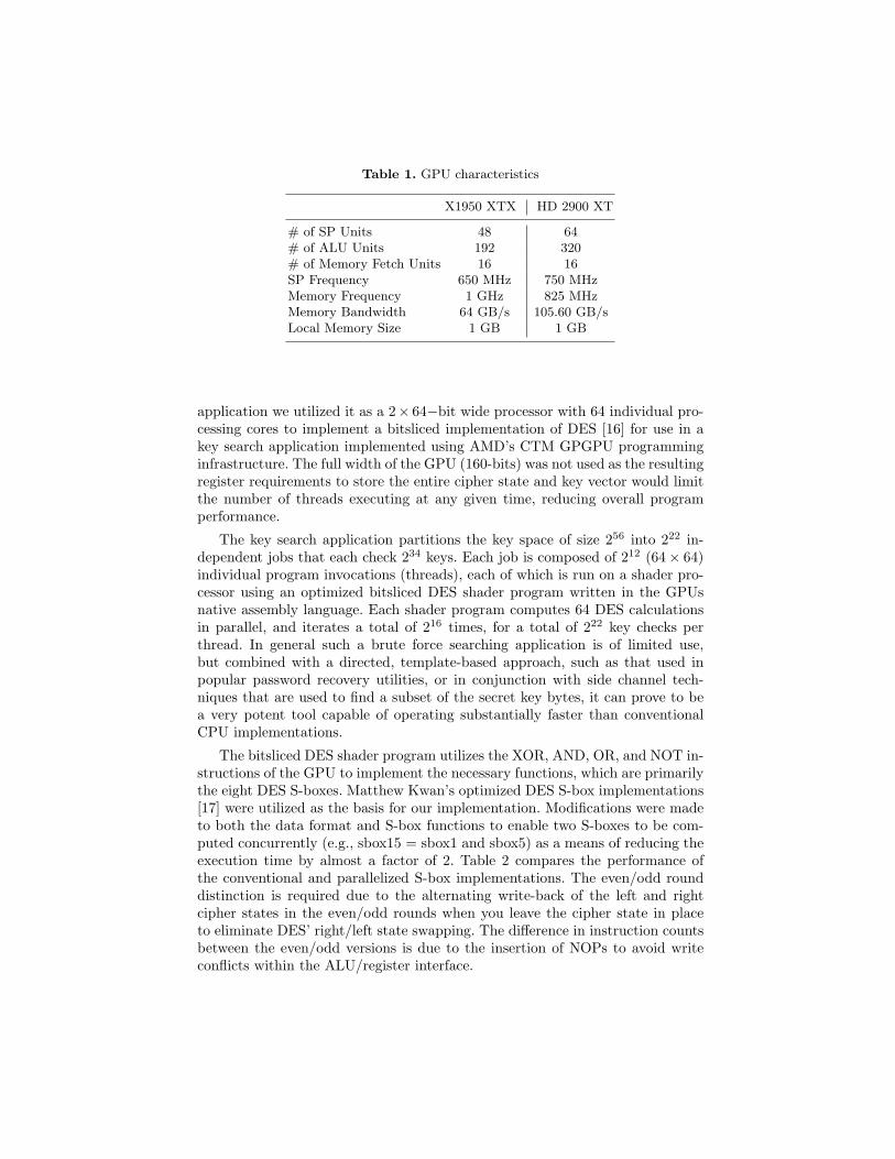
Table 1. GPU characteristics
X1950 XTX HD 2900 XT
# of SP Units 48 64# of ALU Units 192 320# of Memory Fetch Units 16 16SP Frequency 650 MHz 750 MHzMemory Frequency 1 GHz 825 MHzMemory Bandwidth 64 GB/s 105.60 GB/sLocal Memory Size 1 GB 1 GB
application we utilized it as a 2× 64−bit wide processor with 64 individual pro-cessing cores to implement a bitsliced implementation of DES [16] for use in akey search application implemented using AMD’s CTM GPGPU programminginfrastructure. The full width of the GPU (160-bits) was not used as the resultingregister requirements to store the entire cipher state and key vector would limitthe number of threads executing at any given time, reducing overall programperformance.
The key search application partitions the key space of size 256 into 222 in-dependent jobs that each check 234 keys. Each job is composed of 212 (64× 64)individual program invocations (threads), each of which is run on a shader pro-cessor using an optimized bitsliced DES shader program written in the GPUsnative assembly language. Each shader program computes 64 DES calculationsin parallel, and iterates a total of 216 times, for a total of 222 key checks perthread. In general such a brute force searching application is of limited use,but combined with a directed, template-based approach, such as that used inpopular password recovery utilities, or in conjunction with side channel tech-niques that are used to find a subset of the secret key bytes, it can prove to bea very potent tool capable of operating substantially faster than conventionalCPU implementations.
The bitsliced DES shader program utilizes the XOR, AND, OR, and NOT in-structions of the GPU to implement the necessary functions, which are primarilythe eight DES S-boxes. Matthew Kwan’s optimized DES S-box implementations[17] were utilized as the basis for our implementation. Modifications were madeto both the data format and S-box functions to enable two S-boxes to be com-puted concurrently (e.g., sbox15 = sbox1 and sbox5) as a means of reducing theexecution time by almost a factor of 2. Table 2 compares the performance ofthe conventional and parallelized S-box implementations. The even/odd rounddistinction is required due to the alternating write-back of the left and rightcipher states in the even/odd rounds when you leave the cipher state in placeto eliminate DES’ right/left state swapping. The difference in instruction countsbetween the even/odd versions is due to the insertion of NOPs to avoid writeconflicts within the ALU/register interface.
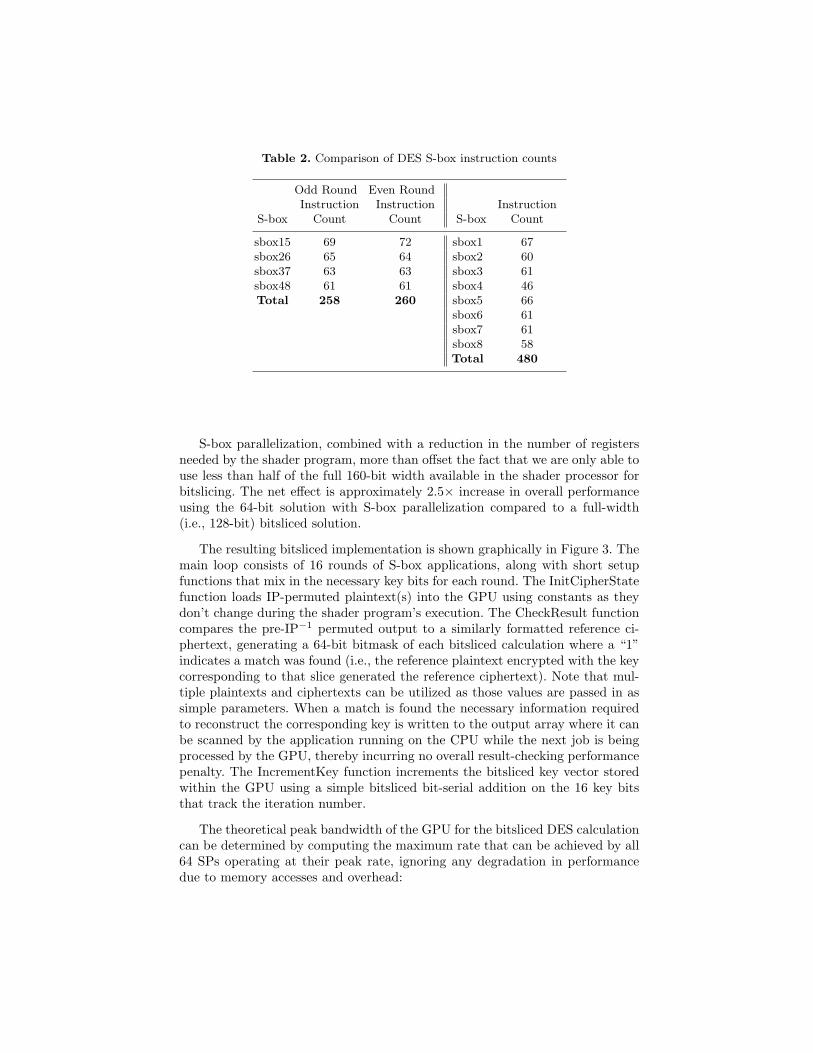
Table 2. Comparison of DES S-box instruction counts
Odd Round Even RoundInstruction Instruction Instruction
S-box Count Count S-box Count
sbox15 69 72 sbox1 67sbox26 65 64 sbox2 60sbox37 63 63 sbox3 61sbox48 61 61 sbox4 46Total 258 260 sbox5 66
sbox6 61sbox7 61sbox8 58Total 480
S-box parallelization, combined with a reduction in the number of registersneeded by the shader program, more than offset the fact that we are only able touse less than half of the full 160-bit width available in the shader processor forbitslicing. The net effect is approximately 2.5× increase in overall performanceusing the 64-bit solution with S-box parallelization compared to a full-width(i.e., 128-bit) bitsliced solution.
The resulting bitsliced implementation is shown graphically in Figure 3. Themain loop consists of 16 rounds of S-box applications, along with short setupfunctions that mix in the necessary key bits for each round. The InitCipherStatefunction loads IP-permuted plaintext(s) into the GPU using constants as theydon’t change during the shader program’s execution. The CheckResult functioncompares the pre-IP−1 permuted output to a similarly formatted reference ci-phertext, generating a 64-bit bitmask of each bitsliced calculation where a “1”indicates a match was found (i.e., the reference plaintext encrypted with the keycorresponding to that slice generated the reference ciphertext). Note that mul-tiple plaintexts and ciphertexts can be utilized as those values are passed in assimple parameters. When a match is found the necessary information requiredto reconstruct the corresponding key is written to the output array where it canbe scanned by the application running on the CPU while the next job is beingprocessed by the GPU, thereby incurring no overall result-checking performancepenalty. The IncrementKey function increments the bitsliced key vector storedwithin the GPU using a simple bitsliced bit-serial addition on the 16 key bitsthat track the iteration number.
The theoretical peak bandwidth of the GPU for the bitsliced DES calculationcan be determined by computing the maximum rate that can be achieved by all64 SPs operating at their peak rate, ignoring any degradation in performancedue to memory accesses and overhead:
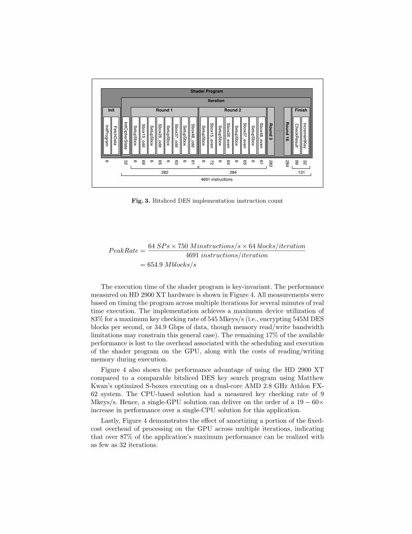
Shader Program
Iteration
Init
FetchData
InitProgram
Round 1
Sbox15_odd
Sbox37_odd
SetupSbox
SetupSbox
Sbox26_odd
SetupSbox
Sbox48_odd
Round 3
Round 16
. . .
Finish
CheckResult
IncrementKey
SetupSbox
Round 2
Sbox15_even
Sbox37_even
SetupSbox
SetupSbox
Sbox26_even
SetupSbox
Sbox48_even
SetupSbox
InitCipherState
69
6 65
6 63
6 61
32
99
6 6 72
6 64
6 63
6 61
6 282
284
32
131284282
4691 instructions
Fig. 3. Bitsliced DES implementation instruction count
PeakRate =64 SPs× 750 Minstructions/s× 64 blocks/iteration
4691 instructions/iteration
= 654.9 Mblocks/s
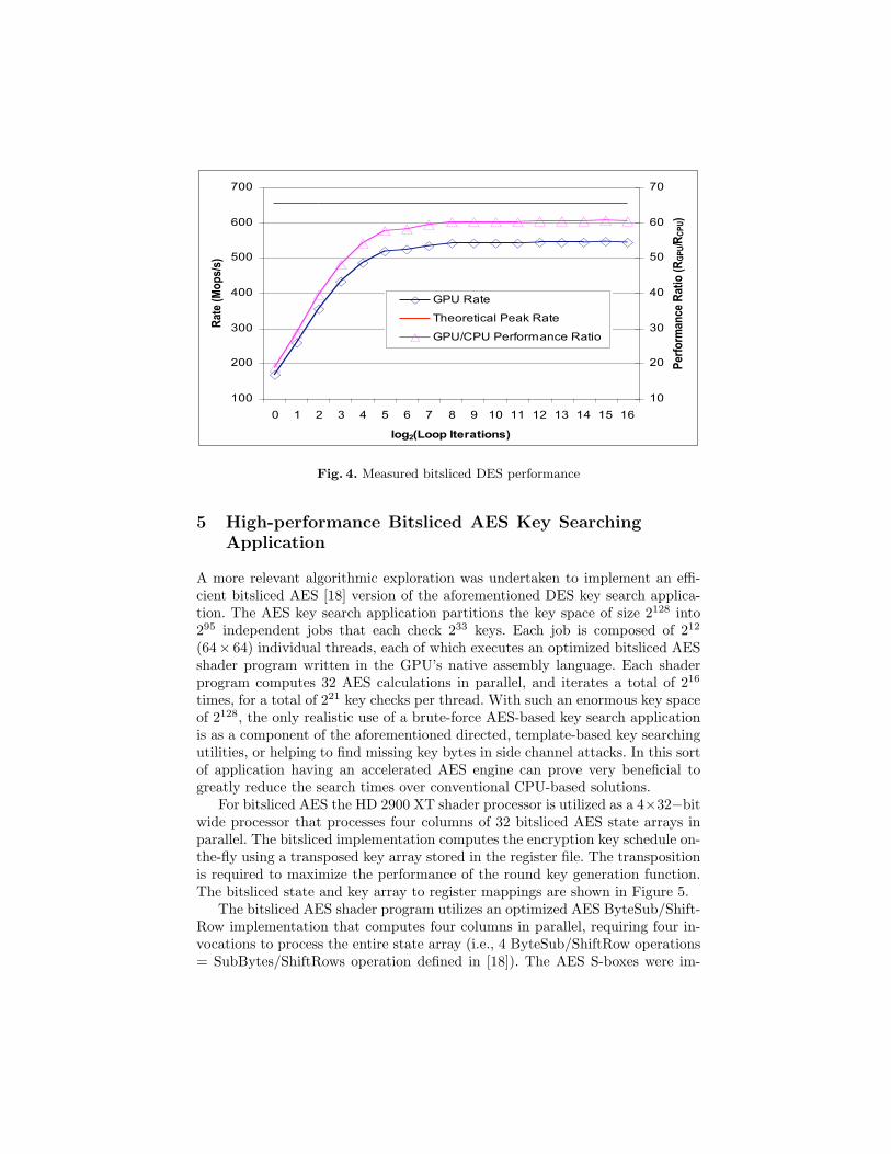
The execution time of the shader program is key-invariant. The performancemeasured on HD 2900 XT hardware is shown in Figure 4. All measurements werebased on timing the program across multiple iterations for several minutes of realtime execution. The implementation achieves a maximum device utilization of83% for a maximum key checking rate of 545 Mkeys/s (i.e., encrypting 545M DESblocks per second, or 34.9 Gbps of data, though memory read/write bandwidthlimitations may constrain this general case). The remaining 17% of the availableperformance is lost to the overhead associated with the scheduling and executionof the shader program on the GPU, along with the costs of reading/writingmemory during execution.
Figure 4 also shows the performance advantage of using the HD 2900 XTcompared to a comparable bitsliced DES key search program using MatthewKwan’s optimized S-boxes executing on a dual-core AMD 2.8 GHz Athlon FX-62 system. The CPU-based solution had a measured key checking rate of 9Mkeys/s. Hence, a single-GPU solution can deliver on the order of a 19 − 60×increase in performance over a single-CPU solution for this application.
Lastly, Figure 4 demonstrates the effect of amortizing a portion of the fixed-cost overhead of processing on the GPU across multiple iterations, indicatingthat over 87% of the application’s maximum performance can be realized withas few as 32 iterations.
100
200
300
400
500
600
700
0 1 2 3 4 5 6 7 8 9 10 11 12 13 14 15 16
log2(Loop Iterations)
Rate (Mops/s)
10
20
30
40
50
60
70
Performance Ratio (RGPU/RCPU)
GPU Rate
Theoretical Peak Rate
GPU/CPU Performance Ratio
Fig. 4. Measured bitsliced DES performance
5 High-performance Bitsliced AES Key SearchingApplication
A more relevant algorithmic exploration was undertaken to implement an effi-cient bitsliced AES [18] version of the aforementioned DES key search applica-tion. The AES key search application partitions the key space of size 2128 into295 independent jobs that each check 233 keys. Each job is composed of 212
(64× 64) individual threads, each of which executes an optimized bitsliced AESshader program written in the GPU’s native assembly language. Each shaderprogram computes 32 AES calculations in parallel, and iterates a total of 216
times, for a total of 221 key checks per thread. With such an enormous key spaceof 2128, the only realistic use of a brute-force AES-based key search applicationis as a component of the aforementioned directed, template-based key searchingutilities, or helping to find missing key bytes in side channel attacks. In this sortof application having an accelerated AES engine can prove very beneficial togreatly reduce the search times over conventional CPU-based solutions.
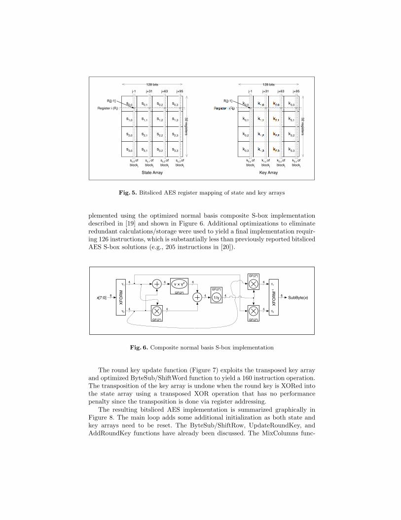
For bitsliced AES the HD 2900 XT shader processor is utilized as a 4×32−bitwide processor that processes four columns of 32 bitsliced AES state arrays inparallel. The bitsliced implementation computes the encryption key schedule on-the-fly using a transposed key array stored in the register file. The transpositionis required to maximize the performance of the round key generation function.The bitsliced state and key array to register mappings are shown in Figure 5.
The bitsliced AES shader program utilizes an optimized AES ByteSub/Shift-Row implementation that computes four columns in parallel, requiring four in-vocations to process the entire state array (i.e., 4 ByteSub/ShiftRow operations= SubBytes/ShiftRows operation defined in [18]). The AES S-boxes were im-
k0,0 k1,0 k2,0 k3,0
k0,1 k1,1 k2,1 k3,1
k0,2 k1,2 k2,2 k3,2
k0,3 k1,3 k2,3 k3,3
s0,0
s1,0
s2,0
s3,0
s0,1
s1,1
s2,1
s3,1
s0,2
s1,2
s2,2
s3,2
s0,3
s1,3
s2,3
s3,3
Register i (Ri)
j-1 j+31 j+63 j+95
128 bits
Register i (Ri)
j-1 j+31 j+63 j+95
128 bits
32 registers
32 registers
sc,0 of
blockj
State Array
sc,1 of
blockj
sc,2 of
blockj
sc,3 of
blockj
k0,c of
blockj
k1,c of
blockj
k2,c of
blockj
k3,c of
blockj
Key Array
Ri[j-1] Ri[j-1]
Fig. 5. Bitsliced AES register mapping of state and key arrays
plemented using the optimized normal basis composite S-box implementationdescribed in [19] and shown in Figure 6. Additional optimizations to eliminateredundant calculations/storage were used to yield a final implementation requir-ing 126 instructions, which is substantially less than previously reported bitslicedAES S-box solutions (e.g., 205 instructions in [20]).
XFORM
XFORM-1GF(24)
1/γ
GF(24)
GF(24)
4
γ0
γ1
γ0
4
4
4
4
4 4
4
4
88
γ1
GF(24)
x[7:0] SubByte(x)
GF(24)
ν × γ2
Fig. 6. Composite normal basis S-box implementation
The round key update function (Figure 7) exploits the transposed key arrayand optimized ByteSub/ShiftWord function to yield a 160 instruction operation.The transposition of the key array is undone when the round key is XORed intothe state array using a transposed XOR operation that has no performancepenalty since the transposition is done via register addressing.
The resulting bitsliced AES implementation is summarized graphically inFigure 8. The main loop adds some additional initialization as both state andkey arrays need to be reset. The ByteSub/ShiftRow, UpdateRoundKey, andAddRoundKey functions have already been discussed. The MixColumns func-

Key Array
k0,0 k1,0 k2,0 k3,0
ByteSub/ShiftRow
k0,1 k1,1 k2,1 k3,1
k0,2 k1,2 k2,2 k3,2
k0,3 k1,3 k2,3 k3,3
Updated Key Array
k0,0 k1,0 k2,0 k3,0
k0,1 k1,1 k2,1 k3,1
k0,2 k1,2 k2,2 k3,2
k0,3 k1,3 k2,3 k3,3
Rcon[i]
Fig. 7. Round key update function
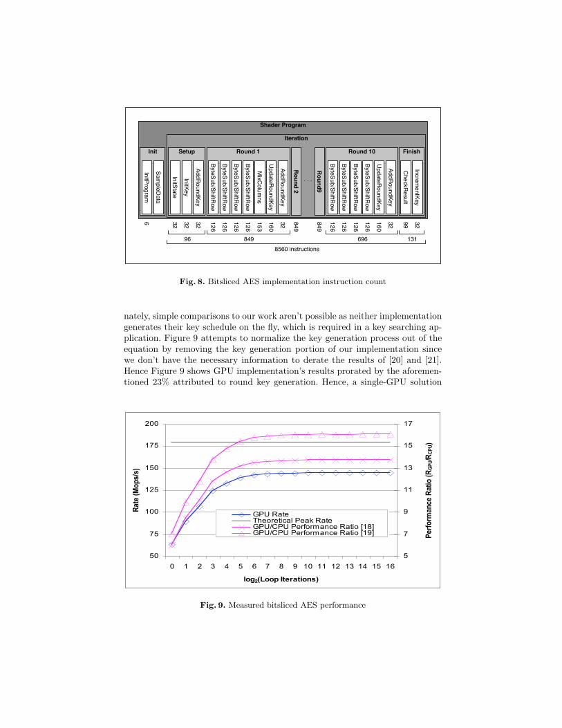
tion processes all four columns in parallel, in-place, and in a single invocation.The CheckResult and IncrementKey functions are functionally equivalent topreviously described bitsliced DES functions. As in the case of DES, arbitraryplaintexts and ciphertexts can be used, and, as previously mentioned, the keyschedule is computed on-the-fly. With pre-generated keys, the performance couldbe increased by 23%.
The theoretical peak bandwidth of the GPU for bitsliced AES calculationscan be computed as with DES using the formula:
PeakRate =64 SPs× 750 Minstructions/s× 32 blocks/iteration
8560 instructions/iteration
= 179.4 Mblocks/s (w/key generation)
The execution time of the shader is key-invariant. The performance measuredon HD 2900 XT hardware is shown in Figure 9. All measurements were basedon timing the program across multiple iterations for several minutes of real timeexecution. The implementation achieves a maximum device utilization of 81% fora maximum key checking rate of 145 Mkeys/s (i.e., encrypting 145M blocks persecond, or 18.5 Gbps of data, though memory read/write bandwidth limitationsmay constrain the general case).
Figure 9 also compares the performance on the GPU to two previously re-ported software implementations ([20], [21]). The authors of [20] describe a non-bitsliced implementation on an AMD Athlon 64 3500+ CPU running @ 2.2 GHzat a rate of 2200 MHz / 170 cycles/block ∼ 13 Mblocks/s. The authors of [21]describe a non-bitsliced implementation on an AMD Opteron 64 CPU running@ 2.4 GHz at a rate of 2400 MHz / 254 cycles/block ∼ 9 Mblocks/s. Unfortu-
Shader Program
Iteration
SetupInit
SampleData
InitState
InitKey
AddRoundKey
InitProgram
Round 1
ByteSub/ShiftR
ow
MixColumns
UpdateRoundKey
ByteSub/ShiftR
ow
ByteSub/ShiftR
ow
ByteSub/ShiftR
ow
AddRoundKey
Round 2
Round9
. . .
Round 10
ByteSub/ShiftR
ow
UpdateRoundKey
ByteSub/ShiftR
ow
ByteSub/ShiftR
ow
ByteSub/ShiftR
ow
AddRoundKey
FinishCheckResult
IncrementKey
32
32
32
126
126
126
126
153
160
32
849
849
126
126
126
126
32
160
32
99
6
131
8560 instructions
69684996
Fig. 8. Bitsliced AES implementation instruction count
nately, simple comparisons to our work aren’t possible as neither implementationgenerates their key schedule on the fly, which is required in a key searching ap-plication. Figure 9 attempts to normalize the key generation process out of theequation by removing the key generation portion of our implementation sincewe don’t have the necessary information to derate the results of [20] and [21].Hence Figure 9 shows GPU implementation’s results prorated by the aforemen-tioned 23% attributed to round key generation. Hence, a single-GPU solution
50
75
100
125
150
175
200
0 1 2 3 4 5 6 7 8 9 10 11 12 13 14 15 16
log2(Loop Iterations)
Rate (Mops/s)
5
7
9
11
13
15
17Performance Ratio (RGPU/RCPU)
GPU RateTheoretical Peak RateGPU/CPU Performance Ratio [18]GPU/CPU Performance Ratio [19]
Fig. 9. Measured bitsliced AES performance
can deliver on the order of 6 − 16× increase in performance over a single-CPUsolution for this application.
As with the bitsliced DES implementation, Figure 9 demonstrates the amor-tization effect of running multiple loop iterations, indicating that over 85% of theapplication’s maximum performance can be realized with as few as 8 iterations.
6 Conventional Block-based AES Implementation
In this section, we describe the implementation of a conventional block-basedAES decryption implementation on both the previous-generation X1950 XTXGPU, which only has floating point ALU units, and the current HD 2900 XTGPU that features an enhanced instruction set with full integer support. Evenwith the availability of full integer support, it is still important to understandimplementations on earlier GPUs because they are still used in low-cost graphicscards.
6.1 Implementation using only Floating Point Hardware
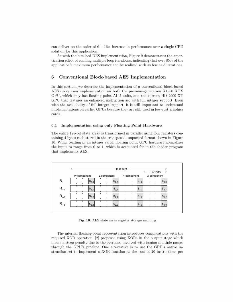
The entire 128-bit state array is transformed in parallel using four registers con-taining 4 bytes each stored in the transposed, unpacked format shown in Figure10. When reading in an integer value, floating point GPU hardware normalizesthe input to range from 0 to 1, which is accounted for in the shader programthat implements AES.
s0,0s1,0s2,0s3,0
s0,1s1,1s2,1s3,1
s0,2s1,2s2,2s3,2
s1,3s2,3s3,3 s0,3
Ri
Ri+1
Ri+2
Ri+3
X componentY componentZ componentW component
128 bits32 bits
Fig. 10. AES state array register storage mapping
The internal floating-point representation introduces complications with therequired XOR operation. [2] proposed using XORs in the output stage whichincurs a steep penalty due to the overhead involved with issuing multiple passesthrough the GPU’s pipeline. One alternative is to use the GPU’s native in-struction set to implement a XOR function at the cost of 20 instructions per
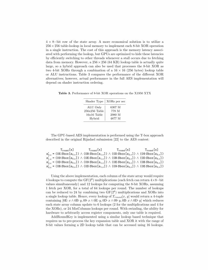
4 × 8−bit row of the state array. A more economical solution is to utilize a256×256 table-lookup in local memory to implement each 8-bit XOR operationin a single instruction. The cost of this approach is the memory latency associ-ated with performing the lookup, but GPUs are optimized to hide these latenciesby efficiently switching to other threads whenever a stall occurs due to fetchingdata from memory. However, a 256× 256 (64 KB) lookup table is actually quitelarge, so a hybrid approach can also be used that processes the 8-bit XOR astwo 4-bit XORs through a combination of a 16 × 16 (256 bytes) lookup tableor ALU instructions. Table 3 compares the performance of the different XORalternatives; however, actual performance in the full AES implementation willdepend on shader instruction ordering.
Table 3. Performance of 8-bit XOR operations on the X1950 XTX
Shader Type XORs per sec
ALU Only 6307 M256x256 Table 778 M16x16 Table 2980 M
Hybrid 4877 M
The GPU-based AES implementation is performed using the T-box approachdescribed in the original Rijndael submission [22] to the AES contest:
Tround[x] Tround[x] Tround[x] Tround[x]s′0,c = (0E·Sbox[s0,c]) ∧ (0B·Sbox[s1,c]) ∧ (0D·Sbox[s2,c]) ∧ (09·Sbox[s3,c])s′1,c = (09·Sbox[s0,c]) ∧ (0E·Sbox[s1,c]) ∧ (0B·Sbox[s2,c]) ∧ (0D·Sbox[s3,c])s′2,c = (0D·Sbox[s0,c]) ∧ (09·Sbox[s1,c]) ∧ (0E·Sbox[s2,c]) ∧ (0B·Sbox[s3,c])s′3,c = (0B·Sbox[s0,c]) ∧ (0D·Sbox[s1,c]) ∧ (09·Sbox[s2,c]) ∧ (0E·Sbox[s3,c])
Using the above implementation, each column of the state array would require4 lookups to compute the GF(28) multiplications (each fetch can return 4×8−bitvalues simultaneously) and 12 lookups for computing the 8-bit XORs, assuming1 fetch per XOR, for a total of 64 lookups per round. The number of lookupscan be reduced to 24 by combining two GF(28) multiplications and XORs intoa single lookup table. Hence, every lookup of Tround[x, y] would return a 4-tuplecontaining [0E·x ∧ 0B· y, 09·x ∧ 0E· y, 0D·x ∧ 09· y, 0B·x ∧ 0D· y] which reduceseach state array column update to 6 lookups (2 for the multiplications and 4 forthe XORs), or 24 MixColumns lookups per round. With swizzling, the ability forhardware to arbitrarily access register components, only one table is required.
AddRoundKey is implemented using a similar lookup based technique thatrequires us to pre-process the key expansion table and XOR it with the range of8-bit values forming a 2D lookup table that can be accessed using 16 lookups.
Every byte in every round maps to a specific entry in the key expansion, so everytable access is of the form Tkeyadd[byte value, key entry]. For the last round,which has no MixColumns operation, the S-Box transform is also included.
The following shader program pseudo-code processes one complete columnof the round function:
float4 a, b, t, c0;a = Tround[r0.w, r3.z];b = Tround[r2.y, r1.x];t = XOR(a, b);c0.w = Tkeyadd[t.x, round offset];c0.z = Tkeyadd[t.y, round offset + 1];c0.y = Tkeyadd[t.z, round offset + 2];c0.x = Tkeyadd[t.w, round offset + 3];
Assuming a single lookup per 8-bit XOR, the complete round function is 40lookups.
When the shader program has processed all 10 rounds the 128-bit state arrayis written out to memory. The hardware can write four outputs simultaneously,which is used to write back the state as four, 4×8−bit values, each representinga row in the transposed state array (e.g., sc,0, sc,1, sc,2, or sc,3 in Figure 10).
The measured performance of this straightforward implementation is approx-imately 315 Mbps on a X1950 XTX and 380 Mbps on a HD 2900 XT. This as-sumes all input blocks use the same key and does not include the key expansionwhich can be computed on the CPU in parallel with previous GPU computationssuch that it can be effectively hidden in a well-balanced implementation. Theperformance is limited due to the number of lookups, which can be a penaltyif there are not enough threads and ALU instructions to hide the associatedmemory access latencies. This is why performance does not scale by the numberof ALU units, because both GPUs have the same number of memory fetch units.In addition, the random nature of the fetches due to the mixing properties ofthe AES algorithm impacts the ability of the GPU to use caching to minimizethe memory access latencies of the lookups.
One possible optimization replaces the 2D round processing lookup tableswith a 3D table that incorporates three GF(28) multiplies and two XORs, as wellas a 2D table that incorporates the fourth GF(28) multiply and round key XOR.This reduces the entire round function to 24 lookups. In this mode, performanceincreases to 770 Mbps. However, the memory requirements are greatly increasedas we now need a 256× 256× 256 (16 MB) lookup table.
Taking advantage of latency hiding, a fully optimized shader using hybridXORs performs at 840 Mbps on a X1950 XTX and 990 Mbps on a HD 2900 XT.
6.2 Implementation on the HD 2900 XT
AMD’s HD 2900 XT allows for native integer operations and data types, as wellas the ability to access data structures in memory (i.e., lookup tables) using

integer values. XORs can be computed using the native XOR instruction ofthe GPU, so all 256× 256 byte lookup tables with precomputed XORs from theprevious section can be replaced with much smaller 256×4 byte tables (similar toCPU implementations) and their results summed using explicit XOR operations.Hence, the round operation shader code can be greatly simplified:
float4 c0, r0;c0 = txMCol[r0.w].wzyx ∧ txMCol[r3.z].xwzy ∧
txMCol[r2.y].yxwz ∧ txMCol[r1.x].zyxw;r0 = c0 ∧ Tkeyadd[round offset];
With swizzling, only a single table is needed to represent an entire state arraycolumn update (e.g., four S-Box transforms and four GF(28) multiplies) in onelookup.
The AddRoundKey step requires the key expansion to be stored as a separatelookup table and the XOR is performed in the shader. In the very last round,SubBytes must be performed without the MixColumns. Previously we wouldhave to precompute this into a dedicated lookup table, but now we perform sep-arate lookups for all the S-Box transform values and then a final AddRoundKey.
With these changes, we can achieve rates of 3.5 Gbps on the HD 2900 XTcompared to an optimized bitsliced implementation on a CPU running at 1.6Gbps [20] and the floating point versions on X1950 XTX and HD 2900 XT GPUsrunning at 840 Mbps and 990 Mbps respectively. This is about 2× faster thana CPU and 3.5× faster than the floating point implementation. This is alsocomparable to the performance achieved by [3] using OpenGL on a NVIDIAGeforce 8800. Although the floating point implementation runs at half the rateof the CPU, this is still considerably better than 2.3% found by [2].
7 Conclusion and Future Work
In this work we have demonstrated both that GPUs can execute symmetric keyciphers, and that that they can perform significantly faster than CPUs in certainapplications. Bitsliced DES on a single HD 2900 XT was shown to operate upto 60 times faster than on a CPU, and bitsliced AES was shown to run up to 16times faster.
We also demonstrated the advantages of the latest generation of GPUs overthe previous generation. A block-based GPU implementation of AES runs 4×faster on the latest generation of GPUs versus the previous generation and 2×faster than a CPU version.
It should be noted that the GPU is optimized for algorithms that are parallelin nature with high arithmetic intensity. Hence, when programs must be executedserially, such as when there are dependencies between threads, then CPUs willoutperform GPUs. This will be the case for certain block cipher operating modessuch as CBC encryption due to the dependencies between successive blocks,
unless there are a sufficient number of streams that can be processed in parallelto provide the large number of independent threads required to extract theperformance in the GPU.
We believe that the entire gamut of cryptography is waiting to be exploredwith current and future GPU hardware. Algorithmic exploration awaits on thesymmetric algorithm front with investigations of efficient implementations ofother block/stream ciphers, particularly those amenable to bitsliced implemen-tations that can leverage the large datapath width inherent in modern GPUs.In addition, the word-level integer support should be exploitable in conventionalhashing algorithms to achieve significant performance increases over conven-tional CPUs. One particularly interesting area of potential research is findingefficient mappings of the integer support on the latest generation of GPUs toDH/RSA/ECC, and other generic integer arithmetic algorithms. With proces-sor design trending towards multi-core, and combining CPU(s) and GPU(s) ona single die, the GPU would appear to be a good research platform for futurealgorithm development.
Acknowledgements
We would like to thank Justin Hensley for typesetting and proofreading. Thanksalso to Arcot Preetham and Avi Bleiweiss for proofreading.
References
1. Owens, J.D., Luebke, D., Govindaraju, N., Harris, M., Krger, J., Lefohn, A.E.,Purcell, T.J.: A survey of general-purpose computation on graphics hardware.Computer Graphics Forum 26(1) (2007) 80–113
2. Cook, D., Keromytis, A.: CryptoGraphics: Exploiting Graphics Cards For Security(Advances in Information Security). Springer-Verlag New York, Inc., Secaucus, NJ,USA (2006)
3. Yamanouchi, T.: AES Encryption and Decryption on the GPU. In: GPU Gems 3.Addison-Wesley Professional (August 2007)
4. Seidel, E.: Preparing tomorrows cryptography: Parallel computation via multi-ple processors, vector processing, and multi-cored chips. (Senior Honors Project,Lawrence University)
5. Fournier, J.J.A., Moore, S.W.: A vector approach to cryptography implementation.In: DRMTICS. (2005) 277–297
6. Costigan, N., Scott, M.: Accelerating ssl using the vector processors in ibm’s cellbroadband engine for sony’s playstation 3. Cryptology ePrint Archive, Report2007/061 (2007) http://eprint.iacr.org/.
7. Doggett, M.: Xenos: Xbox 360 gpu. (Game Developers Conference - Europe 2005,http://ati.amd.com/developer/eg05-xenos-doggett-final.pdf)
8. Blythe, D.: The direct3d 10 system. In: SIGGRAPH ’06: ACM SIGGRAPH 2006Papers, New York, NY, USA, ACM Press (2006) 724–734
9. Segal, M., Akeley, K.: Opengl 2.1 specification. Technical report, Silicon GraphicsComputer Systems, Mountain View, CA,USA (2006)
10. McCool, M., Toit, S.D.: Metaprogramming GPUs with Sh. AK Peters Ltd (2004)
11. Buck, I., Foley, T., Horn, D., Sugerman, J., Fatahalian, K., Houston, M., Hanrahan,P.: Brook for gpus: stream computing on graphics hardware. In: SIGGRAPH ’04:ACM SIGGRAPH 2004 Papers, New York, NY, USA, ACM Press (2004) 777–786
12. NVIDIA Corporation: NVIDIA CUDA Programming Guide. (2007)13. Advanced Micro Devices: ATI CTM Technical Reference Manual. (2006)14. Microsoft Corporation: The DirectX Software Development Kit. (2007)15. Biham, E.: A fast new DES implementation in software. Lecture Notes in Computer
Science 1267 (1997) 260–27216. National Institute of Standards and Technology: Data Encryption Standard (DES).
U.S. Department of Commerce, FIPS pub. 46. (1977)17. Kwan, M.: Bitsliced des s-box source code. (http://www.darkside.com.au/
bitslice/index.html)18. National Institute of Standards and Technology: Advanced Encryption Standard
(AES). U.S. Department of Commerce, FIPS pub. 197. (2001)19. Canright, D.: A very compact rijndael s-box. Technical Report NPS-MA-04-001,
(Naval Postgraduate School)20. Matsui, M.: How far can we go on the x64 processors? In: FSE. (2006) 341–35821. Dai, W.: Crypto++ benchmarks for amd64 processor. (http://www.cryptopp.
com/benchmarks-amd64.html)22. Daemen, J., Rijmen, V.: The Design of Rijndael. Springer-Verlag New York, Inc.,
Secaucus, NJ, USA (2002)