Embed Size (px)
Citation preview
SX-Aurora TSUBASA
Architecture Guide
Revision 1.1
NEC CORPORATION, 2018
1-1
About this document
This document covers the basic architecture of the NEC SX-Aurora TSUBASA series, including information on its software visible resources and instruction set. This manual’s content follows: Chapter 1 overview, Chapter 2 system overview. Software visible registers are covered in Chapter 3 and the data types and instruction formats used in NEC SX-Aurora TSUBASA are described in Chapter 4 and 5 respectively. The memory architecture are shown in Chapter 6, and Chapter 7 describes exceptions. The instruction set is described in Chapter 8. Some appendix information including SX-Aurora TSUBASA CPU microarchitecture overview is also provided in this document.
Copyright© 2018 NEC Corporation. All right reserved.
All information in this document is subject to change without notice.
All product, brand, or trade names in this publication are the trademarks or registered trademarks of their respective owners.
1-2
Terminology
VE: Vector Engine, NEC SX-Aurora TSUBASA's vector processing component. It is
PCI express card form factored, consisting of multiple VE cores and the local HBM
memory.
VE core: the core component of the VE. It fetches codes and data from the VE
memory, decodes and executes a program and write data to the VE memory, as its
central processing unit. It also supports a native vector processing capability.
VE memory: High bandwidth memory (HBM) inside the VE, mainly accessed by VE
cores.
VH: Vector Host, an x86 server to accommodate VEs inside. Currently Linux is
supported for its operating system.
VH CPU: CPUs for the VH server. Intel XEON CPU are currently supported.
VI: Vector Island, a VH and VEs installed in the VE. It may have IB (Infiniband) HCAs
for high performance data transfer.
1-3
Contents 1. Overview ............................................................................................................ 1-10
1.1. Overview ..................................................................................................... 1-10
2. Aurora Systems .................................................................................................. 2-11
2.1. Single VI systems ........................................................................................ 2-11
2.1.1. 1-2 VE node systems ........................................................................... 2-11
2.1.2. 4 VE node systems .............................................................................. 2-12
2.1.3. 8 VE node systems .............................................................................. 2-13
2.2. VI cluster systems ....................................................................................... 2-14
3. Registers .............................................................................................................. 3-0
3.1. Overview ....................................................................................................... 3-0
3.2. User Registers .............................................................................................. 3-1
3.2.1. Process Status Word (PSW) .................................................................. 3-1
3.2.2. Instruction Counter (IC) .......................................................................... 3-6
3.2.3. Scalar Register (S) ................................................................................. 3-7
3.2.4. Vector Register (V) ................................................................................. 3-8
3.2.5. Vector Mask Register (VM) .................................................................. 3-10
3.2.6. Vector Index Register (VIXR) ............................................................... 3-12
3.2.7. Vector Length Register (VL) ................................................................. 3-13
3.3. System Registers ........................................................................................ 3-14
3.3.1. Address Translation Buffer (ATB) ......................................................... 3-14
3.3.2. Communication Register Directory (CRD) ............................................ 3-15
3.3.3. Communication Register (CR) .............................................................. 3-16
3.4. Performance Counters ................................................................................ 3-18
4. Data Format ......................................................................................................... 4-0
4.1 Data format ........................................................................................................ 4-0
4.1.1 Fixed-point data ........................................................................................... 4-0
4.1.2 Floating-Point Data ...................................................................................... 4-1
4.1.3 Logical Data ................................................................................................ 4-4
4.2 Fixed-Point Arithmetic and Shift Operations ....................................................... 4-5
4.2.1 Addition and Subtraction .............................................................................. 4-5
4.2.2 Multiplication ................................................................................................ 4-8
4.2.3 Division ...................................................................................................... 4-10
4.2.4 Comparison ............................................................................................... 4-11
4.2.5 Compare and select operation ................................................................... 4-13
4.2.6 Arithmetic Shift .......................................................................................... 4-15
4.2.7 Logical Shift ............................................................................................... 4-20
4.3 Floating-Point Arithmetic Operations ................................................................ 4-25
4.3.1 Addition and Subtraction ............................................................................ 4-25
4.3.2 Multiplication .............................................................................................. 4-25
4.3.3 Division ...................................................................................................... 4-26
4.3.4 Square Root .............................................................................................. 4-26
4.3.5 Fused multiply add .................................................................................... 4-26
4.3.6 Reciprocal Approximation .......................................................................... 4-26
4.3.7 Reciprocal Square Root Approximation ..................................................... 4-27
4.3.8 Comparison ............................................................................................... 4-27
4.3.9 Compare and select operation ................................................................... 4-27
4.4 Format Conversion........................................................................................... 4-28
4.1.1. Floating-point data to fixed-point data ................................................... 4-28
4.1.2. Fixed-point data to floating-point data ................................................... 4-30
4.1.3. Floating-point data to Floating-point data ............................................. 4-31
4.4 Arithmetic Exception ........................................................................................ 4-33
4.4.1 Floating-point overflow ............................................................................... 4-33
4.1.4. Floating-point underflow ....................................................................... 4-33
4.1.5. Fixed-point overflow ............................................................................. 4-34
4.1.6. Division by zero .................................................................................... 4-34
1-4 4.1.7. Invalid operation ................................................................................... 4-35
4.1.8. Inexact ................................................................................................. 4-35
5. Instruction Format ................................................................................................ 5-0
RM Type .................................................................................................................. 5-0
5.1.1. RM type x field ....................................................................................... 5-1
5.1.2. RM type y field ....................................................................................... 5-2
5.1.3. RM type z field ....................................................................................... 5-2
5.1.4. RM type D field ....................................................................................... 5-2
5.1.5. Effective Address ................................................................................... 5-3
5.2. RRM Type ..................................................................................................... 5-4
5.2.1. RRM type x field ..................................................................................... 5-4
5.2.2. RRM type y field ..................................................................................... 5-5
5.2.3. RRM type z field ..................................................................................... 5-5
5.2.4. RRM type D field .................................................................................... 5-5
5.2.5. Effective Address ................................................................................... 5-5
5.3. CF Type ........................................................................................................ 5-6
5.3.1. CF type x field ........................................................................................ 5-6
5.3.2. CF type y field ........................................................................................ 5-9
5.3.3. CF type z field ........................................................................................ 5-9
5.3.4. CF type D field ....................................................................................... 5-9
5.3.5. Effective Address ................................................................................... 5-9
5.4. RR Type ...................................................................................................... 5-11
5.4.1. RR type x filed ...................................................................................... 5-11
5.4.2. RR type y field ...................................................................................... 5-12
5.4.3. RR type z field ...................................................................................... 5-13
5.4.4. RR type w field ..................................................................................... 5-14
5.4.5. RR type Vx and Vz field........................................................................ 5-15
5.5. RW Type ..................................................................................................... 5-16
5.6. RVM Type ................................................................................................... 5-18
5.6.1. RVM type x field ................................................................................... 5-18
5.6.2. RVM type y field ................................................................................... 5-19
5.6.3. RVM type z field ................................................................................... 5-19
5.6.4. RVM type w field .................................................................................. 5-20
5.6.5. RVM type Vx and Vy field ..................................................................... 5-20
5.6.6. RVM type instruction ............................................................................ 5-20
5.7. RV Type ...................................................................................................... 5-21
5.7.1. RV type x field ...................................................................................... 5-21
5.7.2. RV type y field ...................................................................................... 5-25
5.7.3. RV type z field ...................................................................................... 5-25
5.7.4. RV type Vx, Vy, Vz, Vw field ................................................................. 5-26
6. Memory Architecture ............................................................................................ 6-0
6.1. Memory Architecture Overview ...................................................................... 6-0
6.2. Address Space .............................................................................................. 6-1
6.2.1. Absolute address space ......................................................................... 6-1
6.3. Types of Memory Access .............................................................................. 6-3
6.3.1. VE core memory accesses ..................................................................... 6-3
6.4. Address Translation ...................................................................................... 6-4
6.4.1. Page size ............................................................................................... 6-4
6.4.2. Partial space .......................................................................................... 6-4
6.4.3. Address translation buffer ....................................................................... 6-4
6.5. Memory Access Ordering .............................................................................. 6-9
6.5.1. Release consistency model .................................................................... 6-9
6.6. Cache Memory ............................................................................................ 6-10
6.6.1. Cache hierarchy ................................................................................... 6-10
6.6.2. Cache coherency ................................................................................. 6-11
6.6.3. Cache control ....................................................................................... 6-12
6.6.4. Cache bypass ...................................................................................... 6-12
1-5 6.6.5. LLC ...................................................................................................... 6-12
6.7. Communication Register ............................................................................. 6-14
6.7.1. Access to CR ....................................................................................... 6-14
6.7.2. Barrier synchronization using CR ......................................................... 6-17
7. Exceptions ............................................................................................................ 7-0
7.1. Exceptions and interrupts .............................................................................. 7-0
7.1.1. Attributes of interrupts ............................................................................ 7-1
7.1.2. Causes of interrupts ............................................................................... 7-2
7.1.3. Fast synchronization debug interrupt flag ............................................... 7-8
8. Instructions ........................................................................................................... 8-0
8.1. Legends ........................................................................................................ 8-0
8.1.1. Desctiption of the function ...................................................................... 8-0
8.1.2. Operators ............................................................................................... 8-0
8.1.3. Keywords and notations ......................................................................... 8-1
8.1.4. Syntax .................................................................................................... 8-2
8.1.5. Endianness ............................................................................................ 8-3
8.1.6. Vector elements ..................................................................................... 8-3
8.2. Load/Store instructions .................................................................................. 8-4
8.2.1. LEA ........................................................................................................ 8-4
8.2.2. LDS ........................................................................................................ 8-6
8.2.3. LDU ........................................................................................................ 8-7
8.2.4. LDL ........................................................................................................ 8-8
8.2.5. LD2B .................................................................................................... 8-10
8.2.6. LD1B .................................................................................................... 8-12
8.2.7. STS ...................................................................................................... 8-14
8.2.8. STU ...................................................................................................... 8-15
8.2.9. STL ...................................................................................................... 8-16
8.2.10. ST2B .................................................................................................... 8-17
8.2.11. ST1B .................................................................................................... 8-18
8.2.12. DLDS ................................................................................................... 8-19
8.2.13. DLDU ................................................................................................... 8-20
8.2.14. DLDL .................................................................................................... 8-21
8.2.15. PFCH ................................................................................................... 8-23
8.2.16. TS1AM ................................................................................................. 8-24
8.2.17. TS2AM ................................................................................................. 8-27
8.2.18. TS3AM ................................................................................................. 8-30
8.2.19. ATMAM ................................................................................................ 8-32
8.2.20. CAS...................................................................................................... 8-34
8.3. Transfer Control Instruction ......................................................................... 8-36
8.3.1. FENCE ................................................................................................. 8-36
8.3.2. SVOB ................................................................................................... 8-39
8.4. Fixed-point Operation Instructions ............................................................... 8-41
8.4.1. ADD ..................................................................................................... 8-41
8.4.2. ADS...................................................................................................... 8-42
8.4.3. ADX...................................................................................................... 8-43
8.4.4. SUB...................................................................................................... 8-44
8.4.5. SBS ...................................................................................................... 8-45
8.4.6. SBX ...................................................................................................... 8-46
8.4.7. MPY ..................................................................................................... 8-47
8.4.8. MPS ..................................................................................................... 8-48
8.4.9. MPX ..................................................................................................... 8-49
8.4.10. MPD ..................................................................................................... 8-50
8.4.11. DIV ....................................................................................................... 8-51
8.4.12. DVS...................................................................................................... 8-52
8.4.13. DVX...................................................................................................... 8-53
8.4.14. CMP ..................................................................................................... 8-54
8.4.15. CPS...................................................................................................... 8-56
1-6 8.4.16. CPX...................................................................................................... 8-58
8.4.17. CMS ..................................................................................................... 8-59
8.4.18. CMX ..................................................................................................... 8-60
8.5. Logical Operation Instructions ..................................................................... 8-61
8.5.1. AND ..................................................................................................... 8-61
8.5.2. OR ....................................................................................................... 8-62
8.5.3. XOR ..................................................................................................... 8-63
8.5.4. EQV ..................................................................................................... 8-64
8.5.5. NND ..................................................................................................... 8-65
8.5.6. MRG..................................................................................................... 8-66
8.5.7. LDZ ...................................................................................................... 8-67
8.5.8. PCNT ................................................................................................... 8-68
8.5.9. BRV...................................................................................................... 8-69
8.5.10. BSWP .................................................................................................. 8-70
8.5.11. CMOV .................................................................................................. 8-71
8.6. Shift Operation Instruction ........................................................................... 8-73
8.6.1. SLL ...................................................................................................... 8-73
8.6.2. SLD ...................................................................................................... 8-74
8.6.3. SRL ...................................................................................................... 8-75
8.6.4. SRD ..................................................................................................... 8-76
8.6.5. SLA ...................................................................................................... 8-77
8.6.6. SLAX .................................................................................................... 8-78
8.6.7. SRA...................................................................................................... 8-79
8.6.8. SRAX ................................................................................................... 8-80
8.7. Floating-Point Arithmetic Instructions .......................................................... 8-81
8.7.1. FAD ...................................................................................................... 8-81
8.7.2. FSB ...................................................................................................... 8-83
8.7.3. FMP ..................................................................................................... 8-85
8.7.4. FDV ...................................................................................................... 8-87
8.7.5. FCP ...................................................................................................... 8-89
8.7.6. FCM ..................................................................................................... 8-91
8.7.7. FAQ...................................................................................................... 8-93
8.7.8. FSQ...................................................................................................... 8-95
8.7.9. FMQ ..................................................................................................... 8-97
8.7.10. FCQ ..................................................................................................... 8-99
8.7.11. FIX ..................................................................................................... 8-101
8.7.12. FIXX ................................................................................................... 8-103
8.7.13. FLT .................................................................................................... 8-105
8.7.14. FLTX .................................................................................................. 8-106
8.7.15. CVS.................................................................................................... 8-107
8.7.16. CVD ................................................................................................... 8-109
8.7.17. CVQ ................................................................................................... 8-111
8.8. Branch Instructions .................................................................................... 8-113
8.8.1. BC ...................................................................................................... 8-113
8.8.2. BCS.................................................................................................... 8-115
8.8.3. BCF .................................................................................................... 8-117
8.8.4. BCR ................................................................................................... 8-119
8.8.5. BSIC................................................................................................... 8-122
8.9. Vector Load/Store and Move Instructions .................................................. 8-124
8.9.1. VLD .................................................................................................... 8-124
8.9.2. VLDU ................................................................................................. 8-126
8.9.3. VLDL .................................................................................................. 8-128
8.9.4. VLD2D ............................................................................................... 8-130
8.9.5. VLDU2D ............................................................................................. 8-132
8.9.6. VLDL2D ............................................................................................. 8-134
8.9.7. VST .................................................................................................... 8-136
8.9.8. VSTU ................................................................................................. 8-138
1-7 8.9.9. VSTL .................................................................................................. 8-140
8.9.10. VST2D ............................................................................................... 8-142
8.9.11. VSTU2D ............................................................................................. 8-144
8.9.12. VSTL2D ............................................................................................. 8-146
8.9.13. VGT.................................................................................................... 8-148
8.9.14. VGTU ................................................................................................. 8-150
8.9.15. VGTL .................................................................................................. 8-152
8.9.16. VSC.................................................................................................... 8-154
8.9.17. VSCU ................................................................................................. 8-156
8.9.18. VSCL .................................................................................................. 8-158
8.9.19. PFCHV ............................................................................................... 8-160
8.9.20. LSV .................................................................................................... 8-162
8.9.21. LVS .................................................................................................... 8-163
8.9.22. LVM.................................................................................................... 8-164
8.9.23. SVM ................................................................................................... 8-165
8.9.24. VBRD ................................................................................................. 8-166
8.9.25. VMV ................................................................................................... 8-168
8.10. Vector Fixed-Point Arithmetic Instructions .............................................. 8-170
8.10.1. VADD ................................................................................................. 8-170
8.10.2. VADS ................................................................................................. 8-172
8.10.3. VADX ................................................................................................. 8-174
8.10.4. VSUB ................................................................................................. 8-175
8.10.5. VSBS ................................................................................................. 8-177
8.10.6. VSBX ................................................................................................. 8-179
8.10.7. VMPY ................................................................................................. 8-180
8.10.8. VMPS ................................................................................................. 8-182
8.10.9. VMPX ................................................................................................. 8-184
8.10.10. VMPD ............................................................................................. 8-185
8.10.11. VDIV ............................................................................................... 8-186
8.10.12. VDVS .............................................................................................. 8-188
8.10.13. VDVX .............................................................................................. 8-190
8.10.14. VCMP ............................................................................................. 8-192
8.10.15. VCPS .............................................................................................. 8-195
8.10.16. VCPX .............................................................................................. 8-198
8.10.17. VCMS ............................................................................................. 8-200
8.10.18. VCMX ............................................................................................. 8-203
8.11. Vector Logical Operation Instructions .................................................... 8-205
8.11.1. VAND ................................................................................................. 8-205
8.11.2. VOR ................................................................................................... 8-207
8.11.3. VXOR ................................................................................................. 8-209
8.11.4. VEQV ................................................................................................. 8-211
8.11.5. VLDZ .................................................................................................. 8-213
8.11.6. VPCNT ............................................................................................... 8-215
8.11.7. VBRV ................................................................................................. 8-217
8.11.8. VSEQ ................................................................................................. 8-219
8.12. Vector Shift Operation Instructions ......................................................... 8-221
8.12.1. VSLL .................................................................................................. 8-221
8.12.2. VSLD .................................................................................................. 8-223
8.12.3. VSRL .................................................................................................. 8-224
8.12.4. VSRD ................................................................................................. 8-226
8.12.5. VSLA .................................................................................................. 8-227
8.12.6. VSLAX ............................................................................................... 8-229
8.12.7. VSRA ................................................................................................. 8-230
8.12.8. VSRAX ............................................................................................... 8-232
8.12.9. VSFA .................................................................................................. 8-233
8.13. Vector Floating-Point Arithmetic Instructions .......................................... 8-234
8.13.1. VFAD ................................................................................................. 8-234
1-8 8.13.2. VFSB .................................................................................................. 8-237
8.13.3. VFMP ................................................................................................. 8-240
8.13.4. VFDV ................................................................................................. 8-243
8.13.5. VFSQRT ............................................................................................ 8-246
8.13.6. VFCP ................................................................................................. 8-248
8.13.7. VFCM ................................................................................................. 8-251
8.13.8. VFMAD .............................................................................................. 8-254
8.13.9. VFMSB ............................................................................................... 8-257
8.13.10. VFNMAD ........................................................................................ 8-260
8.13.11. VFNMSB......................................................................................... 8-263
8.13.12. VRCP ............................................................................................. 8-266
8.13.13. VRSQRT......................................................................................... 8-268
8.13.14. VFIX ............................................................................................... 8-270
8.13.15. VFIXX ............................................................................................. 8-273
8.13.16. VFLT ............................................................................................... 8-275
8.13.17. VFLTX ............................................................................................ 8-278
8.13.18. VCVS .............................................................................................. 8-279
8.13.19. VCVD ............................................................................................. 8-280
8.14. Vector Reduction Instructions ................................................................ 8-281
8.14.1. VSUMS .............................................................................................. 8-281
8.14.2. VSUMX .............................................................................................. 8-283
8.14.3. VFSUM .............................................................................................. 8-285
8.14.4. VMAXS .............................................................................................. 8-287
8.14.5. VMAXX .............................................................................................. 8-289
8.14.6. VFMAX ............................................................................................... 8-291
8.14.7. VRAND .............................................................................................. 8-294
8.14.8. VROR ................................................................................................. 8-295
8.14.9. VRXOR .............................................................................................. 8-296
8.15. Vector Iterative Operation Instructions ................................................... 8-297
8.15.1. VFIA ................................................................................................... 8-297
8.15.2. VFIS ................................................................................................... 8-299
8.15.3. VFIM .................................................................................................. 8-301
8.15.4. VFIAM ................................................................................................ 8-303
8.15.5. VFISM ................................................................................................ 8-305
8.15.6. VFIMA ................................................................................................ 8-307
8.15.7. VFIMS ................................................................................................ 8-309
8.16. Vector Merger Operation Instructions .................................................... 8-311
8.16.1. VMRG ................................................................................................ 8-311
8.16.2. VSHF ................................................................................................. 8-313
8.16.3. VCP.................................................................................................... 8-315
8.16.4. VEX .................................................................................................... 8-317
8.17. Vector Mask Operation Instructions ....................................................... 8-319
8.17.1. VFMK ................................................................................................. 8-319
8.17.2. VFMS ................................................................................................. 8-321
8.17.3. VFMF ................................................................................................. 8-323
8.17.4. ANDM ................................................................................................ 8-325
8.17.5. ORM................................................................................................... 8-326
8.17.6. XORM ................................................................................................ 8-327
8.17.7. EQVM ................................................................................................ 8-328
8.17.8. NNDM ................................................................................................ 8-329
8.17.9. NEGM ................................................................................................ 8-330
8.17.10. PCVM ............................................................................................. 8-331
8.17.11. LZVM .............................................................................................. 8-332
8.17.12. TOVM ............................................................................................. 8-333
8.18. Vector Control instructions ..................................................................... 8-334
8.18.1. LVL .................................................................................................... 8-334
8.18.2. SVL .................................................................................................... 8-335
1-9 8.18.3. SMVL ................................................................................................. 8-336
8.18.4. LVIX ................................................................................................... 8-337
8.19. Control Instructions ................................................................................ 8-338
8.19.1. SIC ..................................................................................................... 8-338
8.19.2. LPM.................................................................................................... 8-339
8.19.3. SPM ................................................................................................... 8-341
8.19.4. LFR .................................................................................................... 8-342
8.19.5. SFR .................................................................................................... 8-343
8.19.6. SMIR .................................................................................................. 8-344
8.19.7. NOP ................................................................................................... 8-345
8.19.8. MONC ................................................................................................ 8-346
8.19.9. LCR .................................................................................................... 8-347
8.19.10. SCR ................................................................................................ 8-348
8.19.11. TSCR .............................................................................................. 8-349
8.19.12. FIDCR ............................................................................................ 8-351
8.20. Host Memory Access Instructions .......................................................... 8-354
8.20.1. LHM ................................................................................................... 8-354
8.20.2. SHM ................................................................................................... 8-356
9. Appendix-1 Microarchitecture of SX-Aurora TSUBASA ........................................ 9-0
9.1. VE CPU ......................................................................................................... 9-0
9.2. Core .............................................................................................................. 9-2
9.3. LLC ............................................................................................................... 9-6
9.4. NoC ............................................................................................................... 9-8
9.5. Ring bus ........................................................................................................ 9-8
9.6. MCU and VE memory.................................................................................... 9-8
9.7. DMU .............................................................................................................. 9-9
9.8. DGU .............................................................................................................. 9-9
9.9. PEU ............................................................................................................... 9-9
9.10. XIU ............................................................................................................ 9-9
10. Appendix-2 List of Instructions ........................................................................ 10-0
10.1. List of SX-Aurora TSUBASA Instructions ................................................. 10-0
11. Appendix-3 Operation Code Table ................................................................ 11-12
11.1. Operation Code Table ............................................................................ 11-12
1-10
1. Overview
1.1. Overview
Simulation of natural or artificial processes has established itself as the third pillar in the
fields of scientific research alongside theories and experiments. Especially in such as
astrophysics, fluid/aerodynamics, applied/organic chemistry, pharmaceuticals and life
science, supercomputing has been playing a major role and indispensable any more.
NEC's innovation platform SX-Aurora TSUBASA is designed to tackle such complex
mathematical, scientific or engineering problems. The NEC proprietary computing
systems provide complete solutions for all sorts of requirements by combining with a
wealth of x86-based products and storage appliances.
NEC SX-Aurora Vector Engine (VE) is for accelerated computing exploiting vector
computing technique proven by NEC's long history of supercomputing, on which a full
application runs on high performance Vector Engines, and only system tasks are taken
care of by the Vector Host (VH), a standard x86 server. With the vector computation
mechanism, large memory bandwidth and a small number of powerful cores, the
architecture gives a strong foundation for high sustained performance.
SX-Aurora TSUBASA Features:
Eight vector cores, a peak performance of 2.45 TFLOPS
Max 48 GB high bandwidth memory (HBM) with 1.2 TB/s memory bandwidth
PCI express generation 3 x 16 lanes for VE-VH communication
2-11
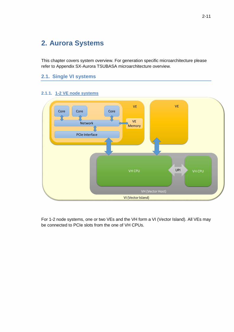
2. Aurora Systems
This chapter covers system overview. For generation specific microarchitecture please
refer to Appendix SX-Aurora TSUBASA microarchitecture overview.
2.1. Single VI systems
2.1.1. 1-2 VE node systems
For 1-2 node systems, one or two VEs and the VH form a VI (Vector Island). All VEs may
be connected to PCIe slots from the one of VH CPUs.
2-12
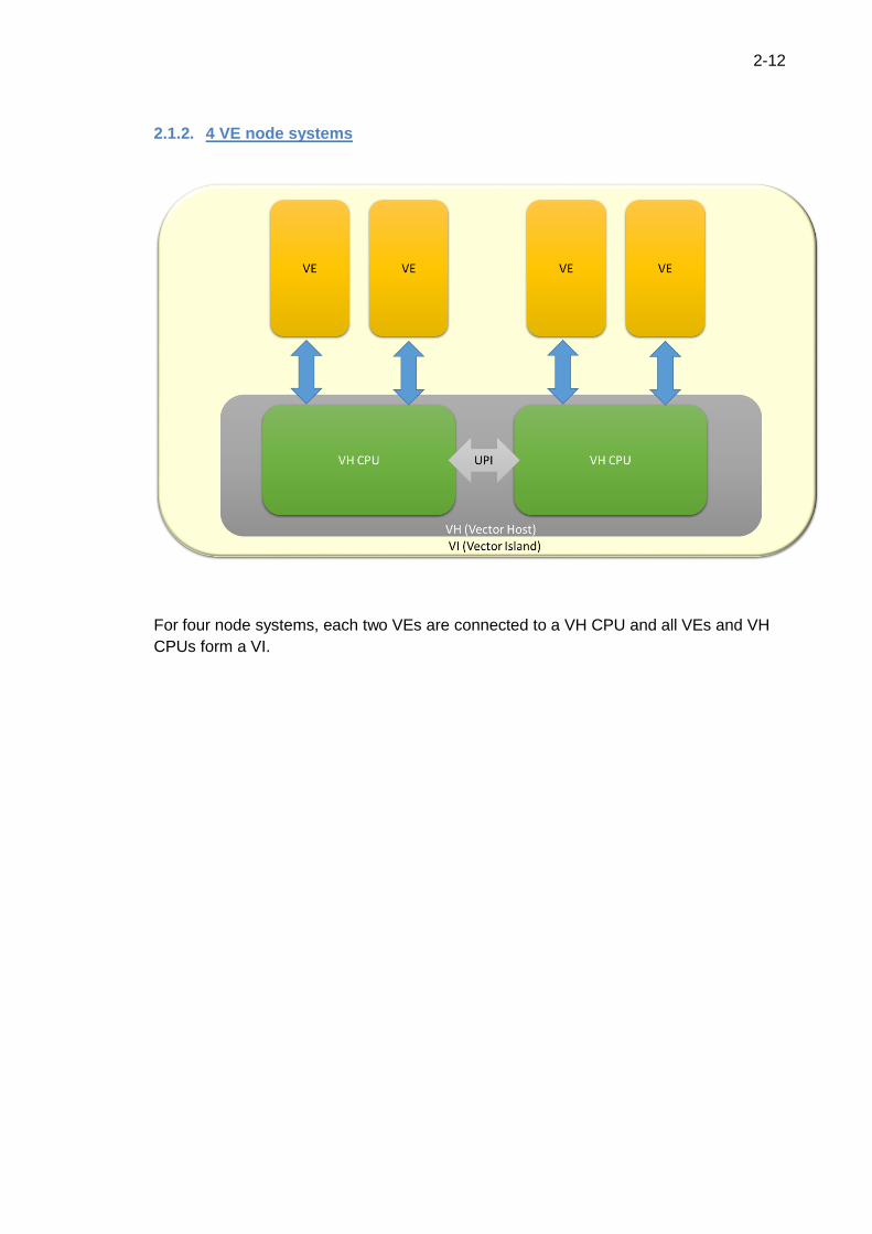
2.1.2. 4 VE node systems
For four node systems, each two VEs are connected to a VH CPU and all VEs and VH
CPUs form a VI.
2-13
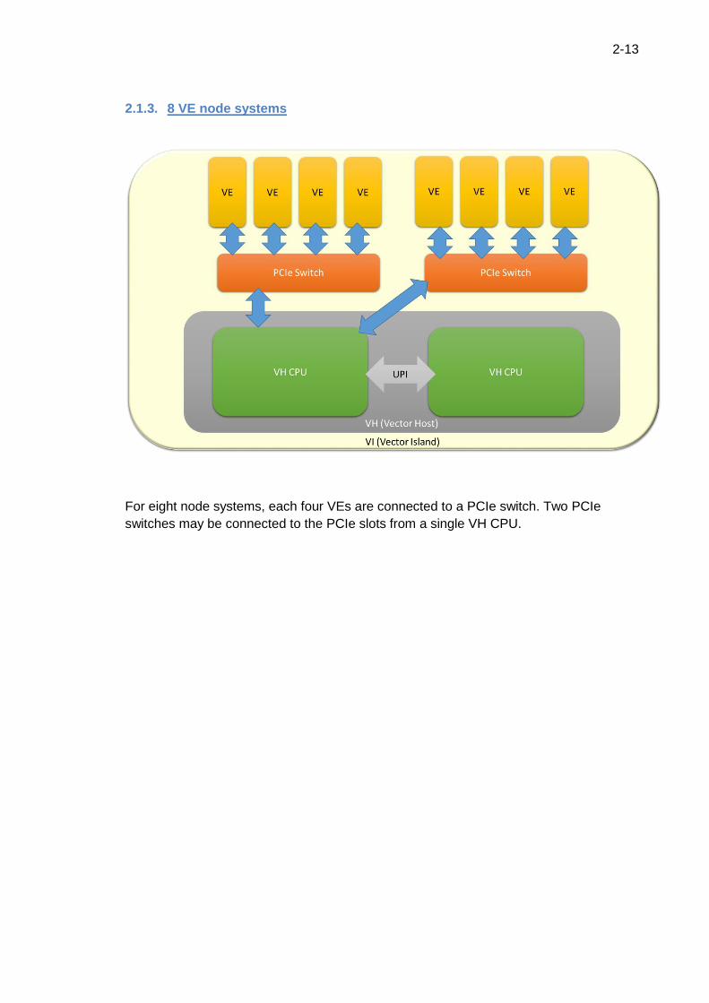
2.1.3. 8 VE node systems
For eight node systems, each four VEs are connected to a PCIe switch. Two PCIe
switches may be connected to the PCIe slots from a single VH CPU.
2-14
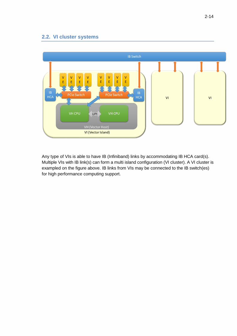
2.2. VI cluster systems
Any type of VIs is able to have IB (Infiniband) links by accommodating IB HCA card(s).
Multiple VIs with IB link(s) can form a multi island configuration (VI cluster). A VI cluster is
exampled on the figure above. IB links from VIs may be connected to the IB switch(es)
for high performance computing support.
3. Registers
3.1. Overview
The Aurora system has three types of software visible registers, user registers, system
registers and system common registers.
The user registers can be accessed by user processes running on a VE core. The
system registers and system common registers are controlled by the VEOS on the VH,
and the access to those registers from user processes is protected by its memory
protection mechanism. The system registers are also used for resource protection in the
Aurora system and are controlled by the resource manager of the VEOS. The system
common registers are unique within a VE CPU and shared by all VE cores on the VE
CPU, whereas each VE core has its own the user and system registers.
3-1
3.2. User Registers
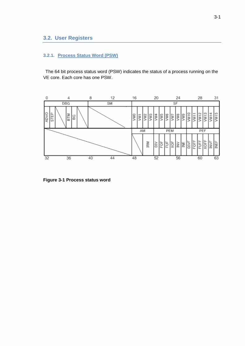
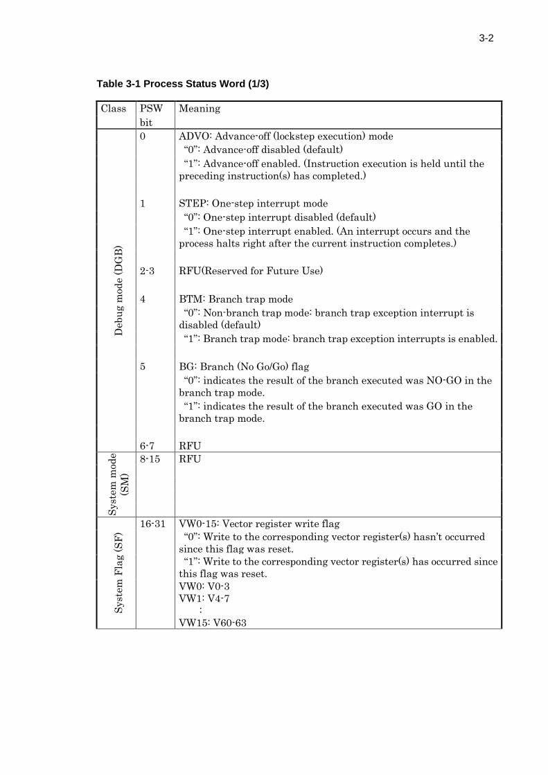
3.2.1. Process Status Word (PSW)
The 64 bit process status word (PSW) indicates the status of a process running on the
VE core. Each core has one PSW.
Figure 3-1 Process status word
3-2
Table 3-1 Process Status Word (1/3)
Class PSW Meaning
bit D
eb
ug m
od
e (
DG
B)
0 ADVO: Advance-off (lockstep execution) mode
“0”: Advance-off disabled (default)
“1”: Advance-off enabled. (Instruction execution is held until the
preceding instruction(s) has completed.)
1 STEP: One-step interrupt mode
“0”: One-step interrupt disabled (default)
“1”: One-step interrupt enabled. (An interrupt occurs and the
process halts right after the current instruction completes.)
2-3 RFU(Reserved for Future Use)
4 BTM: Branch trap mode
“0”: Non-branch trap mode: branch trap exception interrupt is
disabled (default)
“1”: Branch trap mode: branch trap exception interrupts is enabled.
5 BG: Branch (No Go/Go) flag
“0”: indicates the result of the branch executed was NO-GO in the
branch trap mode.
“1”: indicates the result of the branch executed was GO in the
branch trap mode.
6-7 RFU
Syst
em
mod
e
(SM
)
8-15 RFU
Syst
em
Fla
g (
SF
)
16-31 VW0-15: Vector register write flag
“0”: Write to the corresponding vector register(s) hasn’t occurred
since this flag was reset.
“1”: Write to the corresponding vector register(s) has occurred since
this flag was reset.
VW0: V0-3
VW1: V4-7
:
VW15: V60-63
3-3
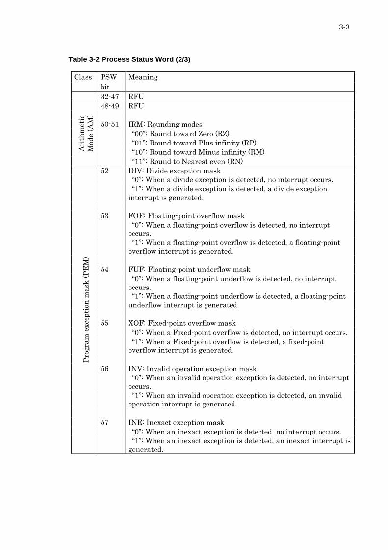
Table 3-2 Process Status Word (2/3)
Class PSW Meaning
bit
32-47 RFU
Ari
thm
eti
c
Mod
e (
AM
)
48-49 RFU
50-51 IRM: Rounding modes
“00”: Round toward Zero (RZ)
“01”: Round toward Plus infinity (RP)
“10”: Round toward Minus infinity (RM)
“11”: Round to Nearest even (RN)
Pro
gra
m e
xce
pti
on
ma
sk (
PE
M)
52 DIV: Divide exception mask
“0”: When a divide exception is detected, no interrupt occurs.
“1”: When a divide exception is detected, a divide exception
interrupt is generated.
53 FOF: Floating-point overflow mask
“0”: When a floating-point overflow is detected, no interrupt
occurs.
“1”: When a floating-point overflow is detected, a floating-point
overflow interrupt is generated.
54 FUF: Floating-point underflow mask
“0”: When a floating-point underflow is detected, no interrupt
occurs.
“1”: When a floating-point underflow is detected, a floating-point
underflow interrupt is generated.
55 XOF: Fixed-point overflow mask
“0”: When a Fixed-point overflow is detected, no interrupt occurs.
“1”: When a Fixed-point overflow is detected, a fixed-point
overflow interrupt is generated.
56 INV: Invalid operation exception mask
“0”: When an invalid operation exception is detected, no interrupt
occurs.
“1”: When an invalid operation exception is detected, an invalid
operation interrupt is generated.
57 INE: Inexact exception mask
“0”: When an inexact exception is detected, no interrupt occurs.
“1”: When an inexact exception is detected, an inexact interrupt is
generated.
3-4
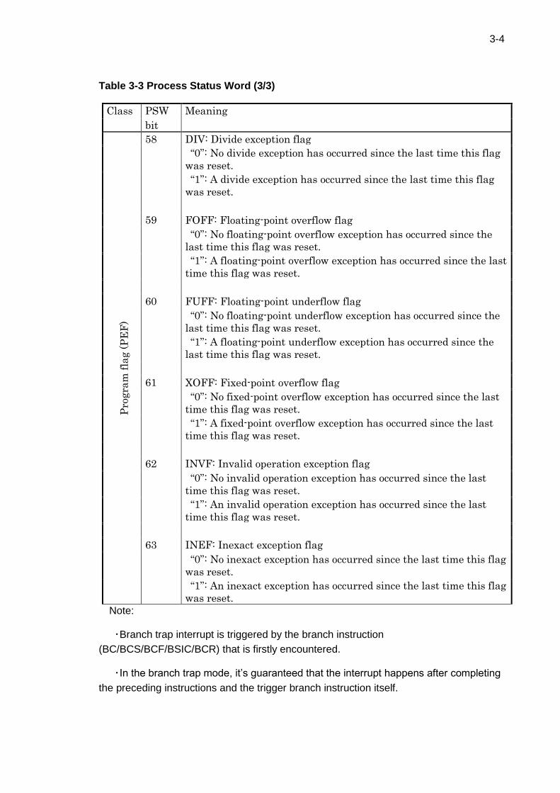
Table 3-3 Process Status Word (3/3)
Class PSW Meaning
bit P
rogra
m f
lag (
PE
F)
58 DIV: Divide exception flag
“0”: No divide exception has occurred since the last time this flag
was reset.
“1”: A divide exception has occurred since the last time this flag
was reset.
59 FOFF: Floating-point overflow flag
“0”: No floating-point overflow exception has occurred since the
last time this flag was reset.
“1”: A floating-point overflow exception has occurred since the last
time this flag was reset.
60 FUFF: Floating-point underflow flag
“0”: No floating-point underflow exception has occurred since the
last time this flag was reset.
“1”: A floating-point underflow exception has occurred since the
last time this flag was reset.
61 XOFF: Fixed-point overflow flag
“0”: No fixed-point overflow exception has occurred since the last
time this flag was reset.
“1”: A fixed-point overflow exception has occurred since the last
time this flag was reset.
62 INVF: Invalid operation exception flag
“0”: No invalid operation exception has occurred since the last
time this flag was reset.
“1”: An invalid operation exception has occurred since the last
time this flag was reset.
63 INEF: Inexact exception flag
“0”: No inexact exception has occurred since the last time this flag
was reset.
“1”: An inexact exception has occurred since the last time this flag
was reset.
Note:
・Branch trap interrupt is triggered by the branch instruction
(BC/BCS/BCF/BSIC/BCR) that is firstly encountered.
・In the branch trap mode, it’s guaranteed that the interrupt happens after completing
the preceding instructions and the trigger branch instruction itself.

3-5
・VW flags may be overly set even when the corresponding vector register(s) is not
actually modified. Writing data to vector registers by other than execution of vector
instructions is not taken account about these flags (e.g. access from the host).
3-6
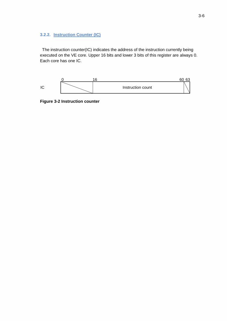
3.2.2. Instruction Counter (IC)
The instruction counter(IC) indicates the address of the instruction currently being
executed on the VE core. Upper 16 bits and lower 3 bits of this register are always 0.
Each core has one IC.
0 16 6360
IC Instruction count
Figure 3-2 Instruction counter
3-7
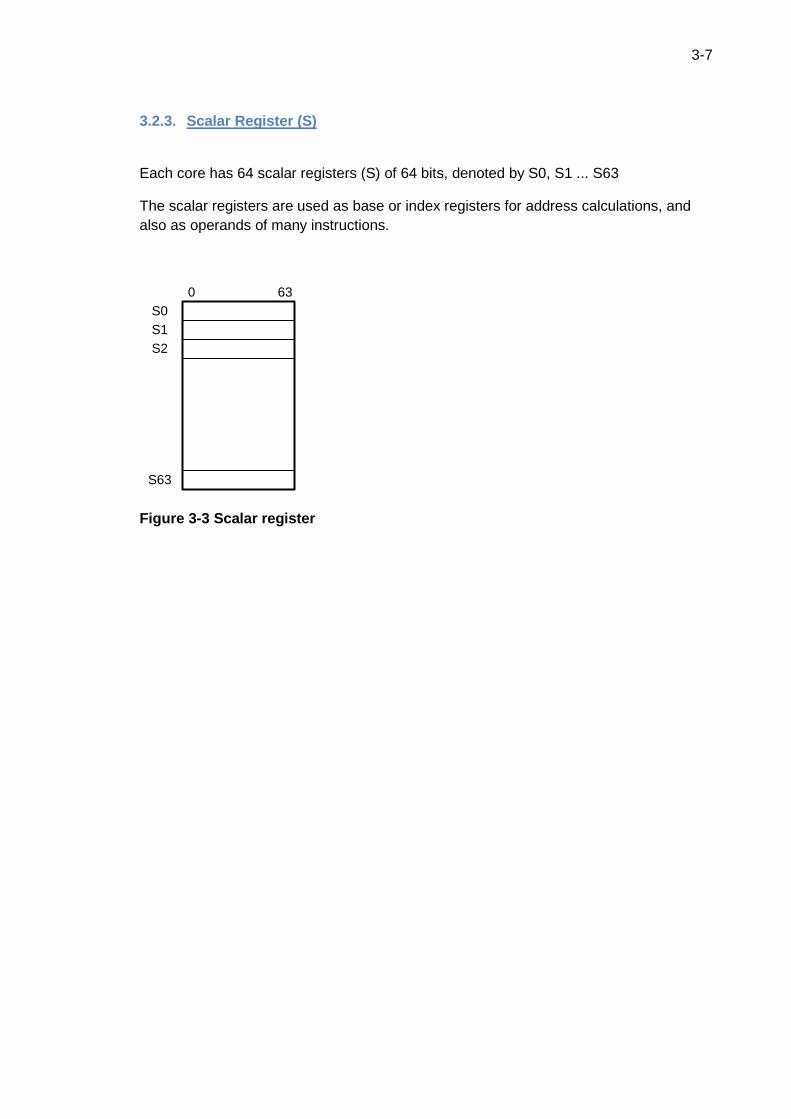
3.2.3. Scalar Register (S)
Each core has 64 scalar registers (S) of 64 bits, denoted by S0, S1 ... S63
The scalar registers are used as base or index registers for address calculations, and
also as operands of many instructions.
0 63
S0
S1
S2
S63
Figure 3-3 Scalar register
3-8
3.2.4. Vector Register (V)
V(Vector Register) is a vector of 64bit registers of the length of MVL. Each core has 64
vector registers denoted by V0, V1 ... V63.
Each 64 bit register in a vector register is called a vector element, or simply an element.
Elements are numbered 0, 1 ... MVL-1 sequentially.
Aurora has various vector instructions such as arithmetic operations between/amongst
vector registers, data transfer operations between vector registers and the main memory.
The number of elements handled by a vector instruction is specified by the VL (Vector
Length) register.
0 63
0
1
2
MVL-1
V0V1
V63
Figure 3-4 Vector register (V)
Note:
・MVL in the SX-Aurora TSUBASA generation 1 is 256.
・In some SX-Aurora documents V0,V1,V2… may be denoted as VR0,VR1,VR2…
・Vector instructions are listed below.
- Vector load/store and move Instructions
- Vector fixed-point arithmetic instructions
- Vector logical operation instructions
- Vector shift operation instructions
- Vector floating-point arithmetic instructions

3-9
- Vector reduction instructions
- Vector iterative operation instructions
- Vector merger operation instructions
- Vector mask operation instructions
3-10
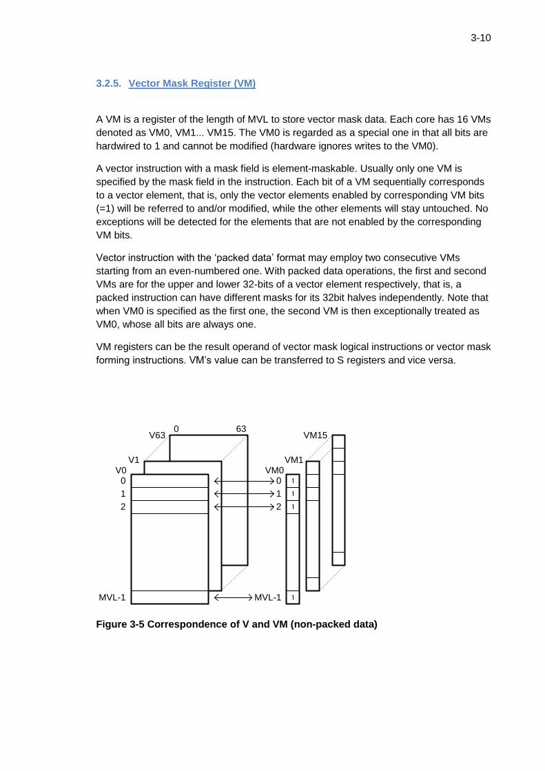
3.2.5. Vector Mask Register (VM)
A VM is a register of the length of MVL to store vector mask data. Each core has 16 VMs
denoted as VM0, VM1... VM15. The VM0 is regarded as a special one in that all bits are
hardwired to 1 and cannot be modified (hardware ignores writes to the VM0).
A vector instruction with a mask field is element-maskable. Usually only one VM is
specified by the mask field in the instruction. Each bit of a VM sequentially corresponds
to a vector element, that is, only the vector elements enabled by corresponding VM bits
(=1) will be referred to and/or modified, while the other elements will stay untouched. No
exceptions will be detected for the elements that are not enabled by the corresponding
VM bits.
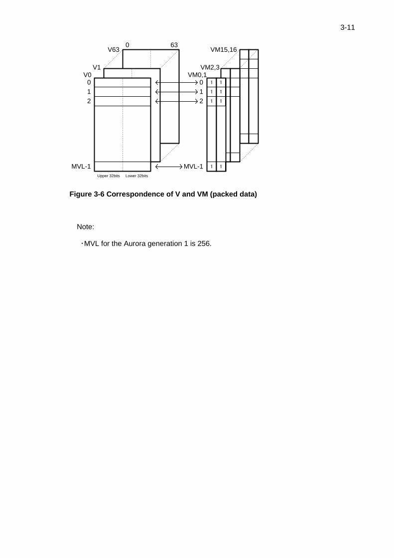
Vector instruction with the ‘packed data’ format may employ two consecutive VMs
starting from an even-numbered one. With packed data operations, the first and second
VMs are for the upper and lower 32-bits of a vector element respectively, that is, a
packed instruction can have different masks for its 32bit halves independently. Note that
when VM0 is specified as the first one, the second VM is then exceptionally treated as
VM0, whose all bits are always one.
VM registers can be the result operand of vector mask logical instructions or vector mask
forming instructions. VM’s value can be transferred to S registers and vice versa.
0 63
0
1
2
MVL-1
V0V1
V63
0
1
2
1MVL-1
1
1
1
VM0VM1
VM15
Figure 3-5 Correspondence of V and VM (non-packed data)
3-11
0 63
0
1
2
MVL-1
V0V1
V63
0
1
2
1MVL-1
1
1
1
VM0,1VM2,3
VM15,16
1
1
1
1
Upper 32bits Lower 32bits
Figure 3-6 Correspondence of V and VM (packed data)
Note:
・MVL for the Aurora generation 1 is 256.
3-12
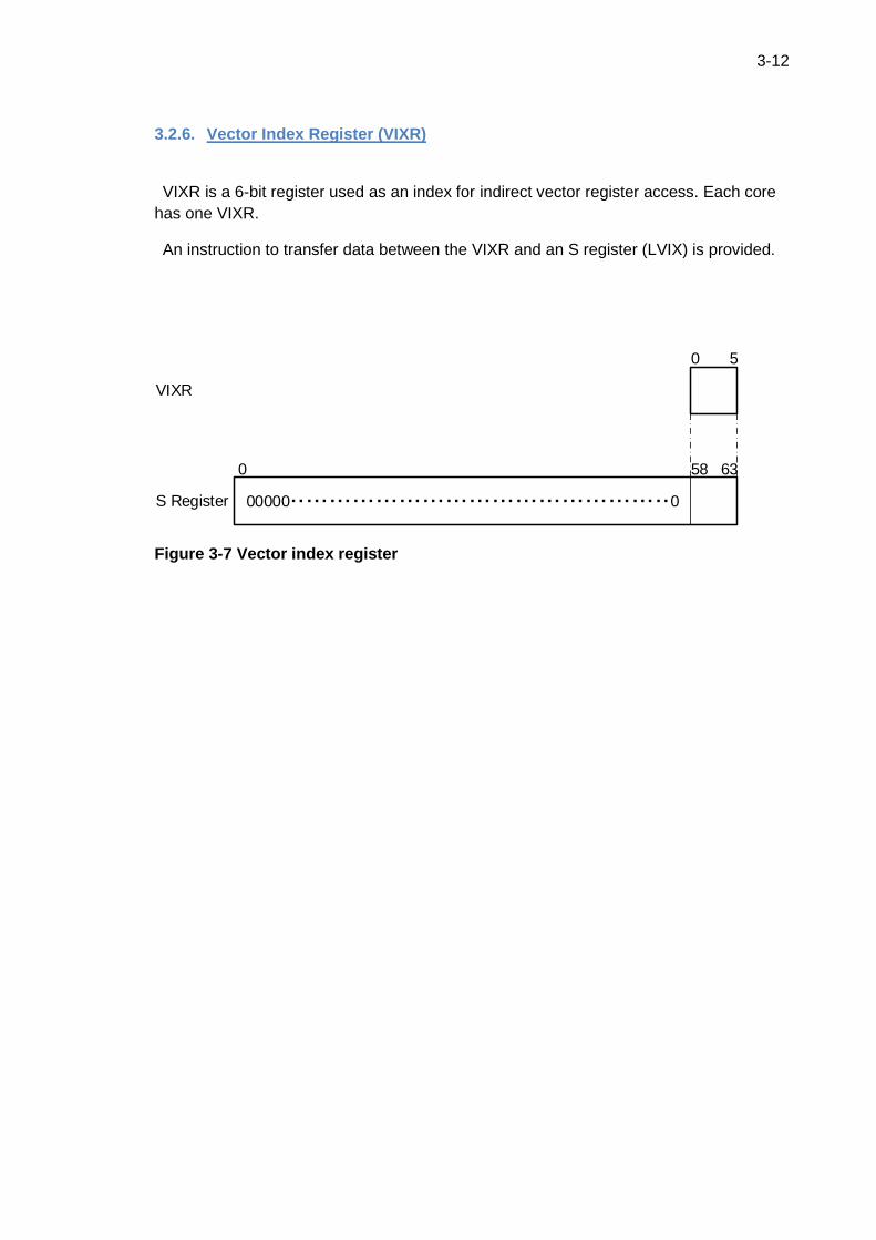
3.2.6. Vector Index Register (VIXR)
VIXR is a 6-bit register used as an index for indirect vector register access. Each core
has one VIXR.
An instruction to transfer data between the VIXR and an S register (LVIX) is provided.
0 6358
50
00000・・・・・・・・・・・・・・・・・・・・・・・・・・・・・・・・・・・・・・・・・・・・・・・・・0
VIXR
S Register
Figure 3-7 Vector index register
3-13
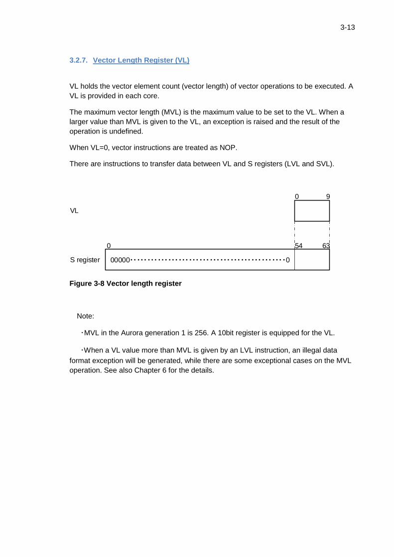
3.2.7. Vector Length Register (VL)
VL holds the vector element count (vector length) of vector operations to be executed. A
VL is provided in each core.
The maximum vector length (MVL) is the maximum value to be set to the VL. When a
larger value than MVL is given to the VL, an exception is raised and the result of the
operation is undefined.
When VL=0, vector instructions are treated as NOP.
There are instructions to transfer data between VL and S registers (LVL and SVL).
0 6354
90
00000・・・・・・・・・・・・・・・・・・・・・・・・・・・・・・・・・・・・・・・・・・・・・0
VL
S register
Figure 3-8 Vector length register
Note:
・MVL in the Aurora generation 1 is 256. A 10bit register is equipped for the VL.
・When a VL value more than MVL is given by an LVL instruction, an illegal data
format exception will be generated, while there are some exceptional cases on the MVL
operation. See also Chapter 6 for the details.
3-14
3.3. System Registers
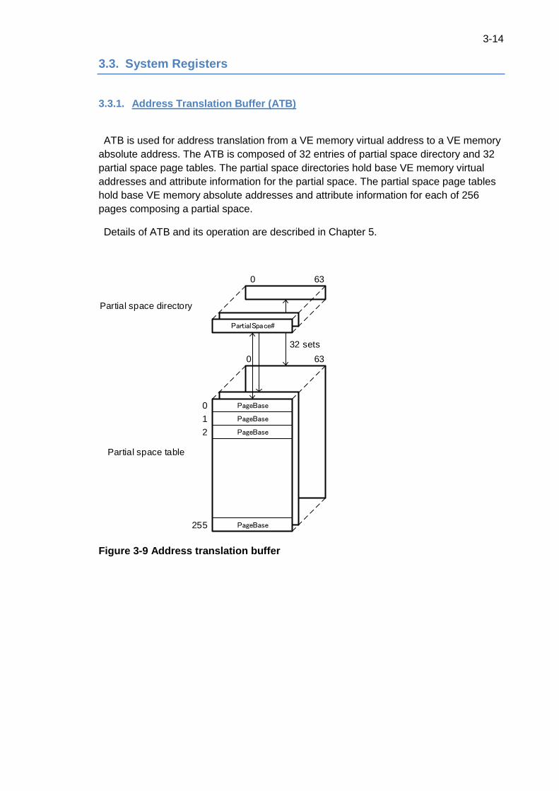
3.3.1. Address Translation Buffer (ATB)
ATB is used for address translation from a VE memory virtual address to a VE memory
absolute address. The ATB is composed of 32 entries of partial space directory and 32
partial space page tables. The partial space directories hold base VE memory virtual
addresses and attribute information for the partial space. The partial space page tables
hold base VE memory absolute addresses and attribute information for each of 256
pages composing a partial space.
Details of ATB and its operation are described in Chapter 5.
0 63
0
1
2
PageBase255
PageBase
PageBase
PageBase
Partial space directory
Partial space table
0 63
PartialSpace#
32 sets
Figure 3-9 Address translation buffer
3-15
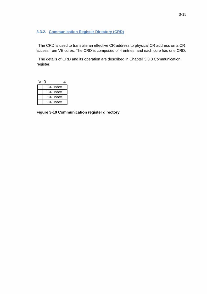
3.3.2. Communication Register Directory (CRD)
The CRD is used to translate an effective CR address to physical CR address on a CR
access from VE cores. The CRD is composed of 4 entries, and each core has one CRD.
The details of CRD and its operation are described in Chapter 3.3.3 Communication
register.
V 0 4CR index
CR index
CR index
CR index
Figure 3-10 Communication register directory
3-16
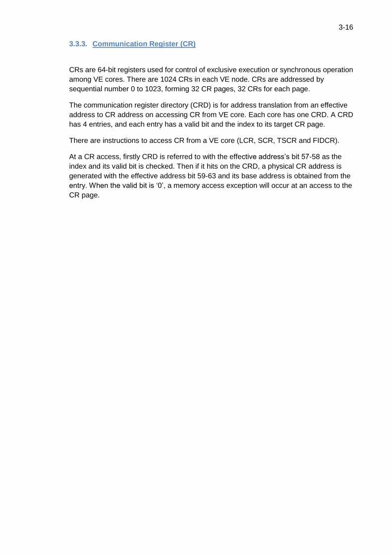
3.3.3. Communication Register (CR)
CRs are 64-bit registers used for control of exclusive execution or synchronous operation
among VE cores. There are 1024 CRs in each VE node. CRs are addressed by
sequential number 0 to 1023, forming 32 CR pages, 32 CRs for each page.
The communication register directory (CRD) is for address translation from an effective
address to CR address on accessing CR from VE core. Each core has one CRD. A CRD
has 4 entries, and each entry has a valid bit and the index to its target CR page.
There are instructions to access CR from a VE core (LCR, SCR, TSCR and FIDCR).
At a CR access, firstly CRD is referred to with the effective address’s bit 57-58 as the
index and its valid bit is checked. Then if it hits on the CRD, a physical CR address is
generated with the effective address bit 59-63 and its base address is obtained from the
entry. When the valid bit is ‘0’, a memory access exception will occur at an access to the
CR page.
3-17
~~
32W
32W
32W
32W
32W
32W
~~
0 63
Communication
Registers
0
32
64
96
128
160
992
1023
57 59 63
CR Directory
V 0 4
Effective address
Figure 3-11 Communication register and communication register directory
Note:
・The base address (index) of a CR page is equivalent to the upper 5-bits of 10-bit CR
address.
・The CRD has four entries to CR pages. A VE core can access maximum 128 CRs
without updating the CRD.
・Bit 0-56 of an effective address is ignored at CR accesses (should be zero.)
3-18
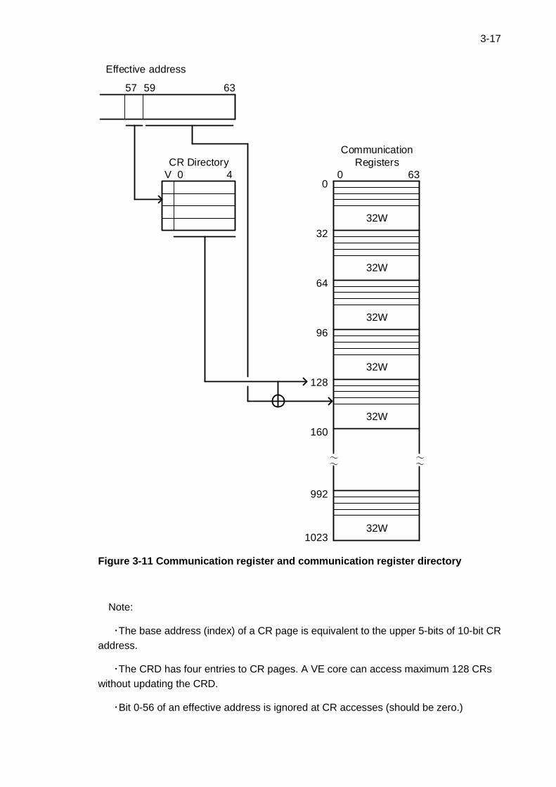
3.4. Performance Counters
SX-Aurora TSUBASA provides performance monitor counters (PMCs) shown below, for
each core. These are default performance indicators and may change due to other
settings
PMC Target event
PMC00 Execution count (EX)
PMC01 Vector execution count (VX)
PMC02 Floating point data element count (FPEC)
PMC03 Vector elements count (VE)
PMC04 Vector execution clock count (VECC)
PMC05 L1 cache miss clock count (L1MCC)
PMC06 Vector elements count 2(VE2)
PMC07 Vector arithmetic execution clock count (VAREC)
PMC08 Vector load execution clock count (VLDEC)
PMC09 Port conflict clock count (PCCC)
PMC10 Vector Load Packet Count (VLPC)
PMC11 Vector load element count (VLEC)
PMC12 Vector load cache miss element count (VLCME)
PMC13 Fused multiply add element count (FMAEC)
PMC14 Power throttling clock count (PTCC)
PMC15 Thermal throttling clock count (TTCC)
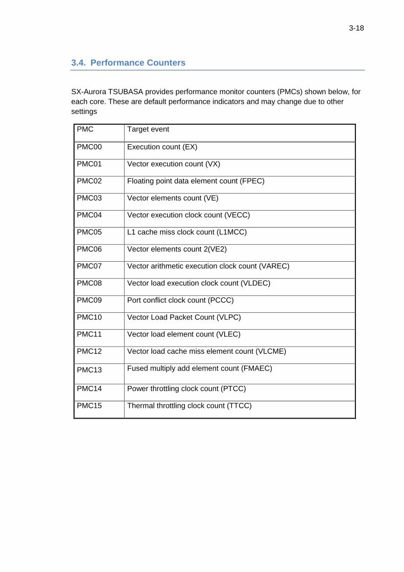
4. Data Format
This chapter describes the data formats and how the operations are performed on data.
The source operand is the input data source of an instruction which may be a scalar
register, immediate value, or vector register. The destination register may be a scalar
register or vector register.
4.1 Data format
4.1.1 Fixed-point data
These four types of fixed point integer are supported.
310
32-bit unsigned
binary integer
310
S
1
630
630
S
32-bit signed
binary integer
64-bit unsigned
binary integer
64-bit signed
binary integer
Binary integer
Binary integer
(negative number is two's
complement)
Binary integer
Binary integer
(negative number is two's complement)
In a signed binary integer, the leftmost bit represents the sign; 0 means positive and 1 is
negative. A negative integer is represented in the form of the complement of two.
4-1
4.1.2 Floating-Point Data
Single-precision data format (32bit), double-precision data format (64bit) and
quadruple-precision floating-point data format (128bit) complying with the IEEE754
standards are supported.
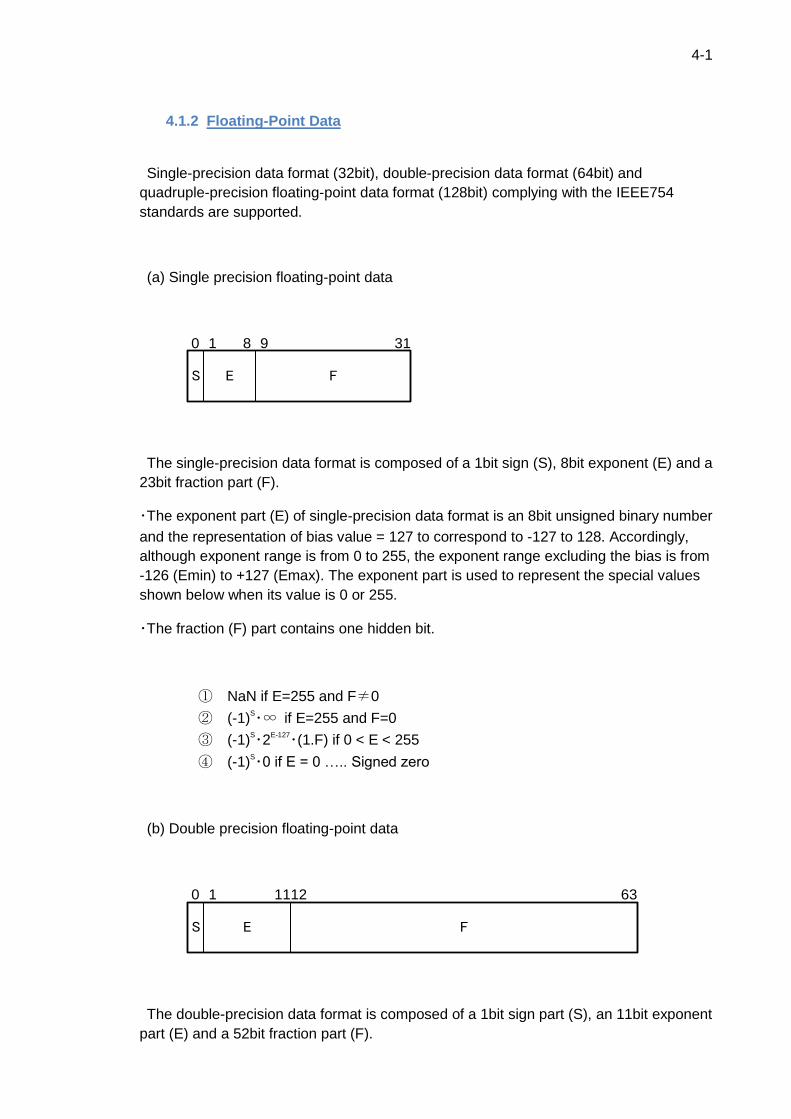
(a) Single precision floating-point data
310
S
1
E F
8 9
The single-precision data format is composed of a 1bit sign (S), 8bit exponent (E) and a
23bit fraction part (F).
・The exponent part (E) of single-precision data format is an 8bit unsigned binary number
and the representation of bias value = 127 to correspond to -127 to 128. Accordingly,
although exponent range is from 0 to 255, the exponent range excluding the bias is from
-126 (Emin) to +127 (Emax). The exponent part is used to represent the special values
shown below when its value is 0 or 255.
・The fraction (F) part contains one hidden bit.
① NaN if E=255 and F≠0
② (-1)S・∞ if E=255 and F=0
③ (-1)S・2E-127・(1.F) if 0 < E < 255
④ (-1)S・0 if E = 0 ….. Signed zero
(b) Double precision floating-point data
630
S
1
E F
1112
The double-precision data format is composed of a 1bit sign part (S), an 11bit exponent
part (E) and a 52bit fraction part (F).

4-2
・The exponent part (E) is an 11bit unsigned binary and the representation of bias value =
1023 to correspond to -1023 to 1024. Accordingly, although exponent range is from 0 to
2047, the exponent range excluding the bias is from -1022 (Emin) to +1023 (Emax),
because the exponent part is used to represent the special values shown followings
when the part value is 0 or 2047.
・The fraction (F) part contains one hidden bit. Therefore, values represented in 64bit
double precision format are as shown.
①NaN if E = 2047 and F≠0
②(-1)S・∞ if E = 2047 and F=0
③(-1)S・2
E-1023・(1.F) if 0 < E < 2047
④(-1)S・0 if E = 0 …… Signed Zero
4-3
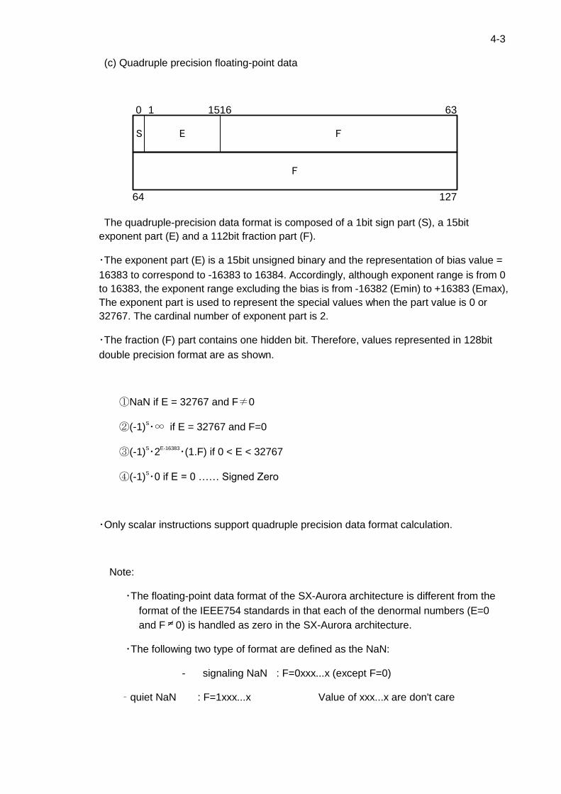
(c) Quadruple precision floating-point data
630
S
1
E F
1516
F
64 127
The quadruple-precision data format is composed of a 1bit sign part (S), a 15bit
exponent part (E) and a 112bit fraction part (F).
・The exponent part (E) is a 15bit unsigned binary and the representation of bias value =
16383 to correspond to -16383 to 16384. Accordingly, although exponent range is from 0
to 16383, the exponent range excluding the bias is from -16382 (Emin) to +16383 (Emax),
The exponent part is used to represent the special values when the part value is 0 or
32767. The cardinal number of exponent part is 2.
・The fraction (F) part contains one hidden bit. Therefore, values represented in 128bit
double precision format are as shown.
①NaN if E = 32767 and F≠0
②(-1)S・∞ if E = 32767 and F=0
③(-1)S・2E-16383・(1.F) if 0 < E < 32767
④(-1)S・0 if E = 0 …… Signed Zero
・Only scalar instructions support quadruple precision data format calculation.
Note:
・The floating-point data format of the SX-Aurora architecture is different from the
format of the IEEE754 standards in that each of the denormal numbers (E=0
and F 0) is handled as zero in the SX-Aurora architecture.
・The following two type of format are defined as the NaN:
- signaling NaN : F=0xxx...x (except F=0)
‐quiet NaN : F=1xxx...x Value of xxx...x are don't care
4-4
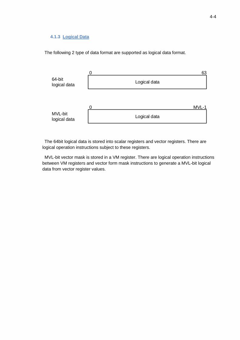
4.1.3 Logical Data
The following 2 type of data format are supported as logical data format.
630
64-bit
logical dataLogical data
MVL-10
MVL-bit
logical dataLogical data
The 64bit logical data is stored into scalar registers and vector registers. There are
logical operation instructions subject to these registers.
MVL-bit vector mask is stored in a VM register. There are logical operation instructions
between VM registers and vector form mask instructions to generate a MVL-bit logical
data from vector register values.
4-5
4.2 Fixed-Point Arithmetic and Shift Operations
The following section describes major fixed-point arithmetic and shift operations. For
details of instructions, refer to Chapter 7.
4.2.1 Addition and Subtraction
There are 6 types of addition and subtraction operations as follows.
(a) 32bit unsigned operation
The bits 32-63 of the source operands are added or subtracted as 32bit unsigned binary
integer. The bits 0-31 of the operands are ignored.
The result is stored into bits 32-63 of the destination register as a 32bit unsigned binary
integer. An overflow is ignored.
The bits 0-31 of the destination register are filled with zero.
(b) 32bit signed operation
The bits 32-63 of the source operands are added or subtracted as 32bit signed binary
integer. The bits 0-31 of the operands are ignored.
The result is stored into bits 32-63 of the destination register as a 32bit signed binary
integer. A fixed-point overflow exception will be raised when the result exceeds
representable range of 32bit signed binary integer. Overflowed bit is discarded.
The bits 0-31 of the destination register are filled with extended sign of the result (bit 32)
or zeros depending on the control field of the instruction.
(c) 64bit unsigned operation
The source operands are added or subtracted as 64bit unsigned binary integer.
The result is stored into the destination register as a 64bit unsigned binary integer. An
overflow is ignored.
(d) 64bit signed operation
The source operands are added or subtracted as 64bit signed binary integer.
4-6
The result is stored into the destination register as a 64bit signed binary integer. A
fixed-point overflow exception is raised when the result exceeds representable range of
64bit signed binary integer. Overflowed bit is discarded.
(e) Packed 32bit unsigned operation
The source operands are separated into upper 32bit and lower 32bit, and each part is
added or subtracted as 32bit unsigned binary integer independently.
The results are stored into the destination register as concatenation of upper and lower
32bit unsigned binary integers. An overflow is ignored.
Either the result of the upper part or the lower part can be masked by 32bits of zero
depending on the control field of instruction.

4-7
(f) Packed 32bit signed operation
The source operands are separated into upper and lower 32bits, then each part is
added or subtracted as 32bit signed binary integer independently.
The results are stored into the destination register as a concatenated value of upper and
lower 32bit signed binary integers. A fixed-point overflow exception is raised when any of
the results exceeds representable range of 32bit signed binary integers. Overflowed bit is
discarded.
Either the result of the upper part or the lower part can be masked by 32bits of zero
depending on the control field of the instruction. In such a case, fixed-point overflow
exception for the masked part is not detected.
4-8
4.2.2 Multiplication
There are 5 types of multiplication operations as follows.
(a) 32bit unsigned operation
The bits 32-63 of the source operands are multiplied as 32bit unsigned binary integer.
The bits 0-31 of the operands are ignored.
The result is stored into bits 32-63 of the destination register as 32bit unsigned binary
integer. An overflow is ignored.
The bits 0-31 of the destination register are filled with zero.
(b) 32bit signed operation
The bits 32-63 of the source operands are multiplied as 32bit signed binary integer.
The bits 0-31 of the operands are ignored.
The result is stored into bits 32-63 of the destination register as 32bit signed binary
integer. A fixed-point overflow exception is raised when the result exceeds representable
range of 32bit signed binary integer. Overflowed bits are discarded.
The bits 0-31 of the destination register are filled with extended sign of the result (bit 32)
or zeros depending on the control field of the instruction.
(c) 32bit signed operation with bit width extension
The bits 32-63 of the source operands are extended to 64bit signed binary integer and
multiplied. The bits 0-31 of the registers are ignored.
The result is stored into the destination register as 64bit signed binary integer. An
overflow doesn’t occur.
(d) 64bit unsigned operation
The source operands are multiplied as 64bit unsigned binary integer.
The result is stored into the destination register as 64bit unsigned binary integer. An
overflow is ignored.
(e) 64bit signed operation
The source operands are multiplied as 64bit signed binary integer.
4-9
The result is stored into the destination register as 64bit signed binary integer. A
fixed-point overflow exception is raised when the result exceeds representable range of
64bit signed binary integer. Overflowed bits are discarded.
4-10
4.2.3 Division
There are 4 types of division operations as follows.
(a) 32bit unsigned operation
The bits 32-63 of the source operands are divided as 32bit unsigned binary integer. The
bits 0-31 of the operands are ignored.
The result is stored into bits 32-63 of the destination register as 32bit unsigned binary
integer. A division exception occurs is raised when the divisor is zero, and the result of
the operation is zero.
The bits 0-31 of the destination register are filled with zero.
(b) 32bit signed operation
The bits 32-63 of the source operands are divided as 32bit signed binary integer. The
bits 0-31 of the operands are ignored.
The result is stored into bits 32-63 of the destination register as 32bit signed binary
integer. A division exception is raised when the divisor is zero, and the result of the
operation is zero. A fixed-point overflow is raised when the result exceeds representable
range of 32bit signed binary integer.
The bits 0-31 of the destination register are filled with extended sign of the result (bit 32)
or zeros depending on the control field of the instruction.
(c) 64bit unsigned operation
The source operands are divided as 64bit unsigned binary integer.
The result is stored into the destination register as 64bit unsigned binary integer. A
division exception is raised when the divisor is zero, and the result of the operation is
zero.
(d) 64bit signed operation
The source operands are divided as 64bit signed binary integer.
The result is stored into the destination register as 64bit signed binary integer. A division
exception is raised when the divisor is zero, and the result of the operation is zero. A
fixed-point overflow is raised when the result exceeds representable range of 32bit
signed binary integer.
4-11
4.2.4 Comparison
There are 6 types of comparison operations as follows.
Result of comparison operation is expressed as follows. Assuming two source operands
as Y and Z, the result is positive non-zero value if Y > Z. Else the result is zero if Y = Z, or
negative value if Y < Z. Regardless of data format of the source operands, the result is
expressed as signed integer.
(a) 32bit unsigned operation
The bits 32-63 of the source operands are compared as 32bit unsigned binary integer.
The bits 0-31 of the operands are ignored.
The result is stored into bits 32-63 of the destination register as 32bit signed binary
integer.
The bits 0-31 of the destination register are filled with zero.
(b) 32bit signed operation
The bits 32-63 of the source operands are compared as 32bit signed binary integer. The
bits 0-31 of the operands are ignored.
The result is stored into bits 32-63 of the destination register as 32bit signed binary
integer.
The bits 0-31 of the destination register are filled with extended sign of the result (bit 32)
or zeros depending on the control field of the instruction.
(c) 64bit unsigned operation
The source operands are compared as 64bit unsigned binary integer.
The result is stored into the destination register as 64bit signed binary integer.
(d) 64bit signed operation
The source operands are compared as 64bit signed binary integer.
The result is stored into the destination register as 64bit signed binary integer.
(e) Packed 32bit unsigned operation

4-12
The source operands are separated into upper 32bit and lower 32bit, and each part is
compared as 32bit unsigned binary integer independently.
The results are stored into the destination register as the concatenation of upper and
lower 32bit signed binary integers.
Either the result of the upper part or the lower part can be masked by 32bits of zero
depending on the control field of instruction.
(f) Packed 32bit signed operation
The source operands are separated into upper 32bit and lower 32bit, then each part is
compared as 32bit signed binary integer independently.
The results are stored into the destination register as the concatenation of upper and
lower 32bit signed binary integers.
Either the result of the upper part or the lower part can be masked by 32bits of zero
depending on the control field of instruction.
4-13
4.2.5 Compare and select operation
There are 4 types of compare and select operations as follows.
(a) 32bit signed operation
The bits 32-63 of the source operands are compared as 32bit signed binary integer, and
selected greater value or lesser value in accordance with control field of the instruction.
The bits 0-31 of the operands are ignored.
The result is stored into the bits 32-63 of the destination register as 32bit signed binary
integer.
The bits 0-31 of the destination register are filled with extended sign of the result (bit 32)
or zeros depending on the control field of the instruction.
(b) 64bit signed operation
The source operands are compared as 64bit signed binary integer, and selected greater
value or lesser value in accordance with control field of the instruction.
The result is stored into the destination register as 64bit signed binary integer.
(c) Packed 32bit unsigned operation
The source operands are separated into upper 32bit and lower 32bit, and each part is
compared as 32bit unsigned binary integer, and selected greater value or lesser value in
accordance with control field of the instruction independently.
The results are stored into the destination register as the concatenation of upper and
lower 32bit unsigned binary integers.
Either the result of the upper part or the lower part can be masked by 32bits of zero
depending on the control field of instruction.
(d) Packed 32bit signed operation
The source operands are separated into upper 32bit and lower 32bit, then each part is
compared as 32bit signed binary integer, and selected greater value or lesser value in
accordance with control field of the instruction independently.
The results are stored into the destination register as the concatenation of upper and
lower 32bit signed binary integers.
Either the result of the upper part or the lower part can be masked by 32bits of zero
depending on the control field of instruction.

4-14
4-15
4.2.6 Arithmetic Shift
There are 6 types of arithmetic shift operations as follows.
(a) 32bit left arithmetic shift
630
Ignored
630
Input operand
Intermediate value
(After shifted)
3231
3231
630
SSS..........................................SOperation result
(sign extended)
3231
or
000.........0
000.........0
XX...........XSX...........................X
SX...........................XXX...........XIgnored
630
000..........................................0
3231
000.........0
SX...........................X
SX...........................XOperation result
(filled with zeros)
Shifted out
The shift amount and the value to be shifted are given by the bits 59-63 and the bits
32-63 of the source operands respectively. The bits 0-58 of the shift amount operand and
the bits 0-31 of the value to be shifted operand are ignored.
The value is shifted left by the shift amount. The vacant bit positions are filled with zero,
and the bits that would be shifted to bit 31 or upper (lower in bit position) will not be used.
The result is stored into bits 32-63 of the destination register. A fixed-point overflow
exception is raised when discarded shifted out bits or the sign of the result (bit 32)
includes a bit which value are not equal to the sign of the original value’s bit 32.
The bits 0-31 of the destination register are filled with extended sign of the result (bit 32)
or zeros depending on the control field of the instruction.
4-16
(b) 32bit right arithmetic shift
630
Ignored
630
Input operand
Intermediate value
(After shifted)
3231
3231
630
SSS..........................................SOperation result
(sign extended)
3231
or
SS............S
SX................................................X
SX...........................X XX...........XIgnored
630
000..........................................0
3231
Operation result
(filled with zeros)
SS............S SX...........................X
SS............S SX...........................X
Shifted out
The shift amount and the value to be shifted are given by the bits 59-63 and the bits
32-63 of the source operands respectively. The bits 0-58 of the shift amount operand and
the bits 0-31 of the value to be shifted operand are ignored.
The value is shifted right by the shift amount. The vacant bit positions are filled with the
sign of the original (not-shifted) value’s bit 32, and the bits that would be right-shifted out
are discarded.
The result is stored into bits 32-63 of the destination register.
The bits 0-31 of the destination register are filled with extended sign of the result (bit 32)
or zeros depending on the control field of the instruction.
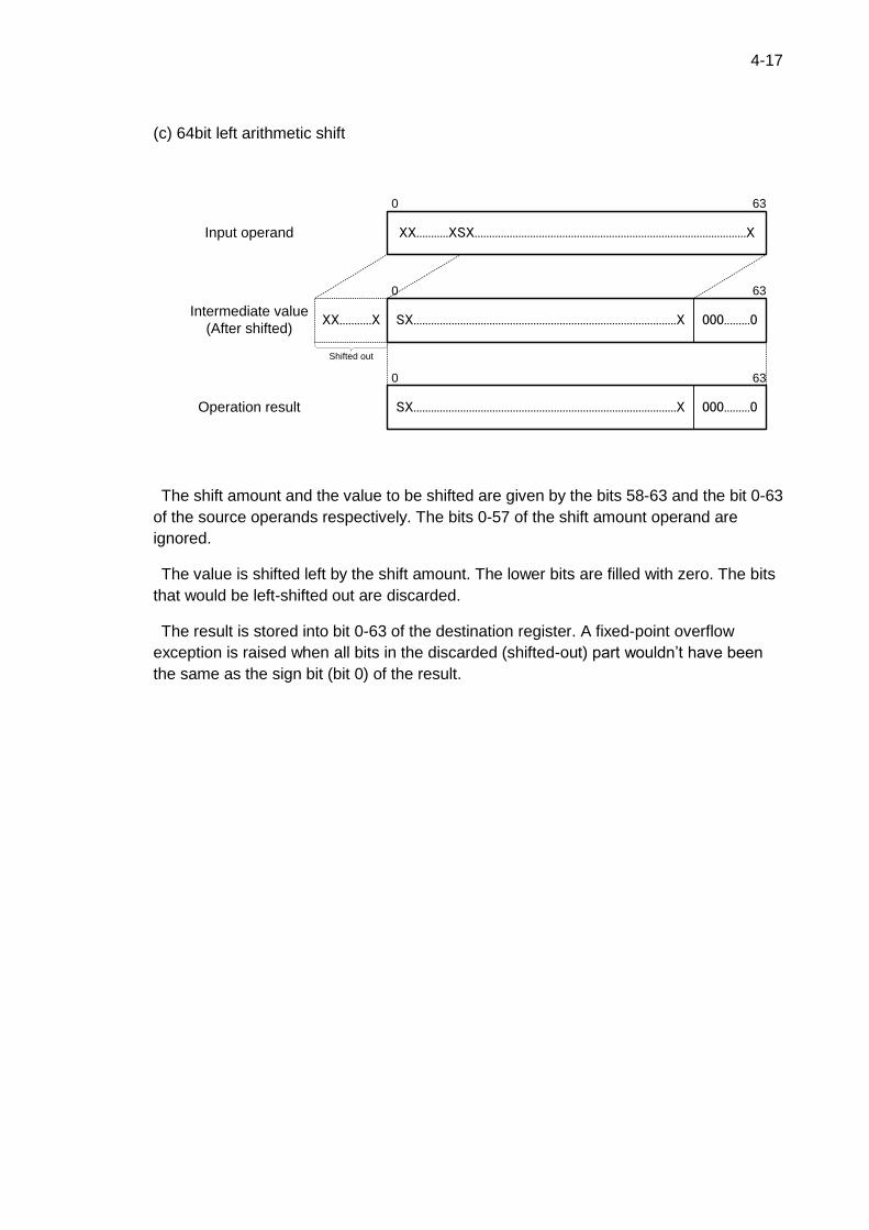
4-17
(c) 64bit left arithmetic shift
630
630
Input operand
Intermediate value
(After shifted)
630
Operation result
000.........0
000.........0
XX...........XSX.............................................................................................X
SX..........................................................................................XXX...........X
SX..........................................................................................X
Shifted out
The shift amount and the value to be shifted are given by the bits 58-63 and the bit 0-63
of the source operands respectively. The bits 0-57 of the shift amount operand are
ignored.
The value is shifted left by the shift amount. The lower bits are filled with zero. The bits
that would be left-shifted out are discarded.
The result is stored into bit 0-63 of the destination register. A fixed-point overflow
exception is raised when all bits in the discarded (shifted-out) part wouldn’t have been
the same as the sign bit (bit 0) of the result.
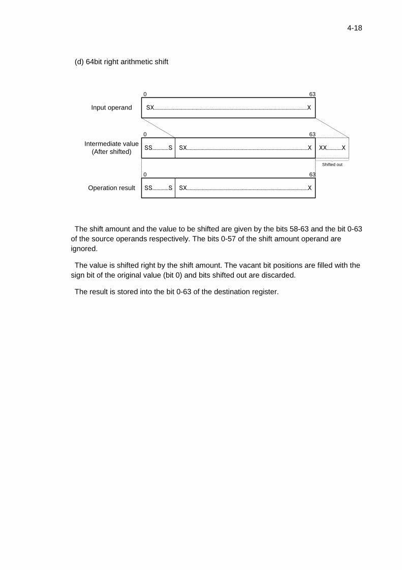
4-18
(d) 64bit right arithmetic shift
630
630
Input operand
Intermediate value
(After shifted)
630
Operation result
SS............S
SX..................................................................................................................X
XX...........X
SS............S
SX..........................................................................................X
SX..........................................................................................X
Shifted out
The shift amount and the value to be shifted are given by the bits 58-63 and the bit 0-63
of the source operands respectively. The bits 0-57 of the shift amount operand are
ignored.
The value is shifted right by the shift amount. The vacant bit positions are filled with the
sign bit of the original value (bit 0) and bits shifted out are discarded.
The result is stored into the bit 0-63 of the destination register.
4-19
(e) Packed 32bit left arithmetic shift
The source operands are separated into upper 32bits and lower 32bits, then each part
may shift independently.
For the upper part, the shift amount and the value to be shifted are given by the bits
27-31 and the bits 0-31 of the source operands respectively. The bits 0-26 of the shift
amount operand are ignored.
For the lower part, the shift amount and the value to be shifted are given by the bits
59-63 and the bits 32-63 of the source operands respectively. The bits 32-58 of the shift
amount operand are ignored.
The results are calculated in the same fashion as (a) operation for the both part.
The results are stored into the destination register as concatenation of upper and lower
32bit signed binary integers. A fixed-point overflow exception is raised when either part of
discarded shifted out bits or the sign of the result includes a bit which value are not equal
to a sign bit of the initial value (bit 0 for the upper part, and bit 32 for the lower part).
Either the result of the upper part or the lower part can be masked by 32bits of zero
depending on the control field of the instruction. In such a case, fixed-point overflow
exception for the masked part is not detected.
(f) Packed 32bit right arithmetic shift
The source operands are separated into upper 32bits and lower 32bits, then each part
may shift independently.
For the upper part, the shift amount and the value to be shifted are given by the bits
27-31 and the bits 0-31 of the source operands respectively. The bits 0-26 of the shift
amount operand are ignored.
For the lower part, the shift amount and the value to be shifted are given by the bits
59-63 and the bits 32-63 of the source operands respectively. The bits 32-58 of the shift
amount operand are ignored.
The results are calculated in the same fashion as (b) operation for the both part.
The results are stored into the destination register as concatenation of upper and lower
32bit signed binary integers.
Either the result of the upper part or the lower part can be masked by 32bits of zero
depending on the control field of the instruction.
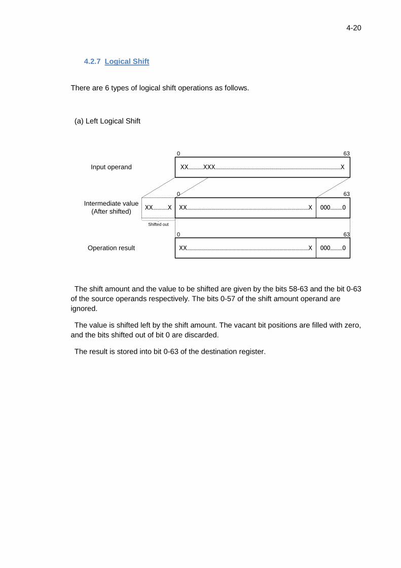
4-20
4.2.7 Logical Shift
There are 6 types of logical shift operations as follows.
(a) Left Logical Shift
630
630
Input operand
Intermediate value
(After shifted)
630
Operation result
000.........0
000.........0
XX...........XXX.............................................................................................X
XX..........................................................................................XXX...........X
XX..........................................................................................X
Shifted out
The shift amount and the value to be shifted are given by the bits 58-63 and the bit 0-63
of the source operands respectively. The bits 0-57 of the shift amount operand are
ignored.
The value is shifted left by the shift amount. The vacant bit positions are filled with zero,
and the bits shifted out of bit 0 are discarded.
The result is stored into bit 0-63 of the destination register.
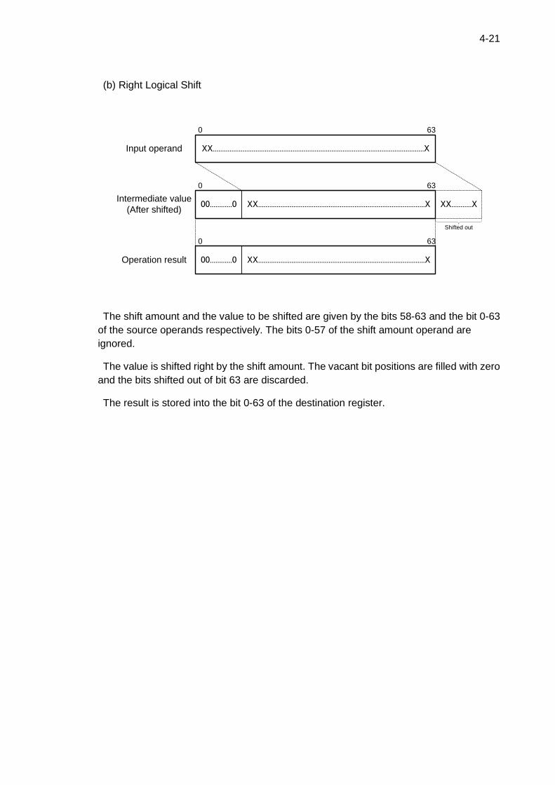
4-21
(b) Right Logical Shift
630
630
Input operand
Intermediate value
(After shifted)
630
Operation result
00............0
XX..................................................................................................................X
XX...........X
00............0
XX..........................................................................................X
XX..........................................................................................X
Shifted out
The shift amount and the value to be shifted are given by the bits 58-63 and the bit 0-63
of the source operands respectively. The bits 0-57 of the shift amount operand are
ignored.
The value is shifted right by the shift amount. The vacant bit positions are filled with zero
and the bits shifted out of bit 63 are discarded.
The result is stored into the bit 0-63 of the destination register.
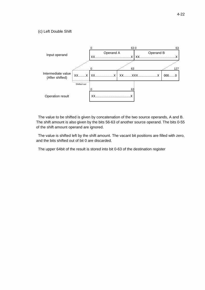
4-22
(c) Left Double Shift
630
Operand A
XX....................................................X
0
Input operand
Intermediate value
(After shifted)
063
63
0
Operation result
63
Operand B
XX....................................................X
XX...........X
XX...................................................X
XX...........................X 000.........0
127
XX............XXX............................X
Shifted out
The value to be shifted is given by concatenation of the two source operands, A and B.
The shift amount is also given by the bits 56-63 of another source operand. The bits 0-55
of the shift amount operand are ignored.
The value is shifted left by the shift amount. The vacant bit positions are filled with zero,
and the bits shifted out of bit 0 are discarded.
The upper 64bit of the result is stored into bit 0-63 of the destination register
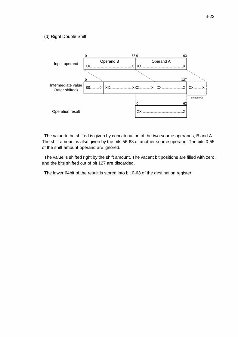
4-23
(d) Right Double Shift
630
1270
Input operand
Intermediate value
(After shifted)
630
Operation result
XX...........X
Operand B
XX....................................................XOperand A
XX....................................................X
063
XX...........................X00............0 XX............................XXX...............X
XX....................................................X
Shifted out
The value to be shifted is given by concatenation of the two source operands, B and A.
The shift amount is also given by the bits 56-63 of another source operand. The bits 0-55
of the shift amount operand are ignored.
The value is shifted right by the shift amount. The vacant bit positions are filled with zero,
and the bits shifted out of bit 127 are discarded.
The lower 64bit of the result is stored into bit 0-63 of the destination register
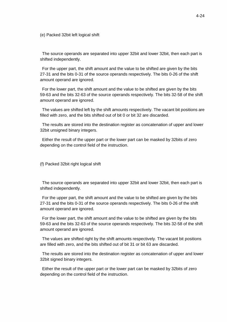
4-24
(e) Packed 32bit left logical shift
The source operands are separated into upper 32bit and lower 32bit, then each part is
shifted independently.
For the upper part, the shift amount and the value to be shifted are given by the bits
27-31 and the bits 0-31 of the source operands respectively. The bits 0-26 of the shift
amount operand are ignored.
For the lower part, the shift amount and the value to be shifted are given by the bits
59-63 and the bits 32-63 of the source operands respectively. The bits 32-58 of the shift
amount operand are ignored.
The values are shifted left by the shift amounts respectively. The vacant bit positions are
filled with zero, and the bits shifted out of bit 0 or bit 32 are discarded.
The results are stored into the destination register as concatenation of upper and lower
32bit unsigned binary integers.
Either the result of the upper part or the lower part can be masked by 32bits of zero
depending on the control field of the instruction.
(f) Packed 32bit right logical shift
The source operands are separated into upper 32bit and lower 32bit, then each part is
shifted independently.
For the upper part, the shift amount and the value to be shifted are given by the bits
27-31 and the bits 0-31 of the source operands respectively. The bits 0-26 of the shift
amount operand are ignored.
For the lower part, the shift amount and the value to be shifted are given by the bits
59-63 and the bits 32-63 of the source operands respectively. The bits 32-58 of the shift
amount operand are ignored.
The values are shifted right by the shift amounts respectively. The vacant bit positions
are filled with zero, and the bits shifted out of bit 31 or bit 63 are discarded.
The results are stored into the destination register as concatenation of upper and lower
32bit signed binary integers.
Either the result of the upper part or the lower part can be masked by 32bits of zero
depending on the control field of the instruction.

4-25
4.3 Floating-Point Arithmetic Operations
The following section describes floating-point arithmetic operations. The arithmetic
operations for floating-point format comply with the IEEE754 standard unless otherwise
noted. Rounding mode for the operations is specified by the IRM field of the PSW. The
detection of floating-point underflow exception is always performed after rounding.
Subnormal numbers are not supported. The result is cut down to zero when an
underflow occurs on the result. When a subnormal number is given by a source operand,
the numbers are also cut down to zero before the execution of the operation.
There are operations for single precision, double precision, and quadruple precision
floating-point data. For the most operations, data format of the source operands and the
result of the operation is the same.
On a single precision floating-point operation, the bits 0-31 of the source operands are
treated as input floating-point values. The result is stored into the bits 0-31 of the
destination register. The bits 32-63 of the source operands are ignored and the bits 32-63
of the destination register are filled with zero.
On a quadruple precision floating-point operation, a source operand is given by
concatenation of the value of consecutive two source scalar register. The result is stored
into consecutive two destination scalar registers.
On a packed single precision floating-point operation, the bits 0-31 and the bits 32-63 of
source operands are treated as input floating-point values individually. The results are
stored into the destination register as concatenation of upper and lower single precision
floating-point data. Either the result of the upper part or the lower part can be masked by
32bits of zero depending on the control field of instruction. In such a case, exceptions for
the masked part are not detected.
The details of instructions are described in the chapter 8.
4.3.1 Addition and Subtraction
There are addition and subtraction operations for single precision, double precision, and
quadruple precision floating-point data.
4.3.2 Multiplication
There are multiplication operations for single precision, double precision, and quadruple
precision floating-point data.

4-26 4.3.3 Division
There are division operations for single precision and double precision floating-point
data. A division exception occurs is raised when the divisor is zero, and the result of the
operation is infinity with the correct sign.
4.3.4 Square Root
There are square root operations for single precision and double precision floating-point
data.
4.3.5 Fused multiply add
There are fused multiply add operations for single precision and double precision
floating-point data.
4.3.6 Reciprocal Approximation
This instruction produces an approximate value for the inverse of the source operand.
There are reciprocal approximation operations for single precision and double precision
floating-point data.
4-27
4.3.7 Reciprocal Square Root Approximation
This instruction produces an approximate value for the inverse square root of the source
operand. There are reciprocal square root approximation operations for single precision
and double precision floating-point data.
4.3.8 Comparison
This instruction produces a comparison result for the source operands. Result of
comparison operation is expressed as follows. Assuming two source operands as Y and
Z, the result is positive non-zero value if Y > Z. Else the result is zero if Y = Z, or negative
value if Y < Z. +0 and -0 are regarded as the same value. Regardless of data format of
the source operands, the result is expressed as signed integer. If any of source operand
has a NaN value, an invalid operation exception is raised and the result is qNaN.
There are comparison operations for single precision, double precision, and quadruple
precision floating-point data. The result of the quadruple precision floating-point
operation is returned by double precision floating-point data.
4.3.9 Compare and select operation
This instruction compares the value of the two source operands, and selects the greater
value or the lesser value in accordance with control field of the instruction. If one of
source operands has a qNaN value and the other has a canonicalized value, the result is
the input value which is not qNaN. If both of source operands has a qNaN value, the
result is qNaN. If any of source operands have a sNaN value, an invalid operation
exception is raised and the result is qNaN. +0 and -0 are regarded as the same value.
The result for the operation for +0 and -0 is defined in chapter 8.
There are compare and select operations for single precision and double precision
floating-point data.
Note:
・On comparison performed by conditional branch (BCF) or mask generation
(VFMF) instructions, NaN input data does not invoke invalid operation
exception.
4-28
4.4 Format Conversion
There are 3 groups of conversion operations, from floating-point data to fixed-point data,
from fixed-point data to floating-point data, and from floating-point data to floating-point
data conversion operations. The conversion operations comply with the IEEE754
standard unless otherwise noted. Rounding mode for the operations is specified by the
IRM field of the PSW or control bits in floating-point data to fixed-point data conversion
instructions. The detection of floating-point underflow exception is always performed after
rounding.
Subnormal numbers are not supported. The result is cut down to zero when an
floating-point underflow occurs on the result. When a subnormal number is given by a
source operand, the numbers are also cut down to zero before the execution of the
operation.
4.1.1. Floating-point data to fixed-point data
There are 4 types of conversion operations from floating-point data to fixed-point data.
An invalid operation exception is raised when the input floating-point data is sNaN,
qNaN, or infinity, or the case that the result of the comparison exceeds representable
range of target fixed-point data format. When an invalid operation exception is raised, the
value of the destination register is unknown.
(a) From single precision floating-point data to 32bit signed binary integer
The bits 0-31 of the source operand are assumed as single precision floating-point data
and converted to 32bit signed binary integer. The bits 32-63 of the operands are ignored.
The result is stored into bits 32-63 of the destination register.
The bits 0-31 of the destination register are filled with extended sign of the result (bit 32)
or zeros depending on the control field of the instruction.
(b) From double precision floating-point data to 32bit signed binary integer
The bit 0-63 of the source operand are assumed as double precision floating-point data
and converted to 32bit signed binary integer.
The result is stored into bits 32-63 of the destination register.
The bits 0-31 of the destination register are filled with extended sign of the result (bit 32)
or zeros depending on the control field of the instruction.

4-29
(c) From double precision floating-point data to 64bit signed binary integer
The bit 0-63 of the source operand are assumed as double precision floating-point data
and converted to 64bit signed binary integer.
The result is stored into bit 0-63 of the destination register.
(d) From packed single precision floating-point data to packed 32bit signed binary
integer
The source operand are separated into upper 32bit and lower 32bit, and each part is
assumed as single precision floating-point data and converted to 32bit signed binary
integer independently.
The results are stored into the destination register as concatenation of upper and lower
32bit signed binary integers. An overflow is ignored.
Either the result of the upper part or the lower part can be masked by 32bits of zero
depending on the control field of instruction. In such a case, exceptions for the masked
part are not detected.
4-30
4.1.2. Fixed-point data to floating-point data
There are 4 types of conversion operations from fixed-point data to floating-point data.
An inexact exception is raised when the conversion results in degradation of the
precision.
(a) From 32bit signed binary integer to single precision floating-point data
The bits 32-63 of the source operand are assumed as 32bit signed fixed-point data and
converted to single precision floating-point data. The bits 0-31 of the operands are
ignored.
The result is stored into bits 0-31 of the destination register.
The bits 32-63 of the destination register are filled with zero.
(b) From 32bit signed binary integer to double precision floating-point data
The bits 32-63 of the source operand are assumed as 32bit signed fixed-point data and
converted to double precision floating-point data. The bits 0-31 of the operands are
ignored.
The result is stored into bit 0-63 of the destination register.
(c) From 64bit signed binary integer to double precision floating-point data
The bit 0-63 of the source operand are assumed as 64bit signed fixed-point data and
converted to double precision floating-point data.
The result is stored into bit 0-63 of the destination register.
(d) From packed 32bit signed binary integer to packed single precision floating-point
data
The source operand are separated into upper 32bit and lower 32bit, and each part is
assumed as 32bit signed binary integer and converted to single precision floating-point
data independently.
The results are stored into the destination register as concatenation of upper and lower
single precision floating-point data.
Either the result of the upper part or the lower part can be masked by 32bits of zero
depending on the control field of instruction. In such a case, exception for the masked
part is not detected.

4-31
4.1.3. Floating-point data to Floating-point data
There are 6 types of conversion operations from floating-point data to floating-point
data.
(a) From double precision floating-point data to single precision floating-point data
The bit 0-63 of the source operand are assumed as double precision floating-point data
and converted to single precision floating-point data.
The result is stored into bits 0-31 of the destination register. The bits 32-63 of the
destination register are filled with zero.
(b) From quadruple precision floating-point data to single precision floating-point data
The concatenation of the two source operands are assumed as quadruple precision
floating-point data and converted to single precision floating-point data.
The result is stored into bits 0-31 of the destination register. The bits 32-63 of the
destination register are filled with zero.
(c) From single precision floating-point data to double precision floating-point data
The bits 0-31 of the source operand are assumed as single precision floating-point data
and converted to double precision floating-point data. The bits 32-63 of the operands are
ignored.
The result is stored into bit 0-63 of the destination register.
(d) From quadruple precision floating-point data to double precision floating-point data
The concatenation of the two source operands are assumed as quadruple precision
floating-point data and converted to double precision floating-point data.
The result is stored into bit 0-63 of the destination register.
(e) From single precision floating-point data to quadruple precision floating-point data
The bits 0-31 of the source operand are assumed as single precision floating-point data
and converted to quadruple precision floating-point data. The bits 32-63 of the operands
are ignored.
The result is stored into bit 0-63 of the two destination registers.

4-32
(f) From double precision floating-point data to quadruple precision floating-point data
The bit 0-63 of the source operand are assumed as double precision floating-point data
and converted to quadruple precision floating-point data.
The result is stored into bit 0-63 of the two destination registers.
4-33
4.4 Arithmetic Exception
The following section describes exceptions raised by floating-point arithmetic
operations.
For vector instructions, exception is raised after operation for all elements are finished,
and the exception is logical OR of the exceptions that is detected on the operations for
each element. For operations for packed data, exceptions detected for the upper part and
the lower part is also ORed.
4.4.1 Floating-point overflow
As a result of the operation, if the exponent exceeds its expressible range in the positive
direction (E> Emax), a floating-point overflow exception occurs. In this case the result is
one of follows depends on the PSW rounding mode:
RZ: The result is formally finite maximum value (E= Emax, F=11...1) with the sign before
rounding.
RN: The result is infinity with the sign before rounding.
RP: When the sign before rounding is positive, the result is +infinity. When the sign
before rounding is negative, the result is formally finite maximum value with a
negative sign.
RM: When the sign before rounding is negative, the result is -infinity. When the sign
before rounding is positive, the result is formally finite maximum value with a positive
sign.
If the floating-point overflow exception mask is enabled, an interrupt occurs. If not,
following instructions are executed.
The floating-point overflow flag (FOFF) is set to 1, regardless of the existence of an
interrupt.
4.1.4. Floating-point underflow
As a result of the operation, if the exponent exceeds its expressible range in the
negative direction (E< Emin), a floating-point underflow exception occurs. The operation
4-34
result is zero with a correct sign. If the floating-point underflow exception mask is enabled,
an interrupt occurs.
If the above mask is not enabled for interrupts, the following instruction is executed.
The floating-point underflow flag (FUFF) is set to 1, regardless of the existence of an
interrupt.
4.1.5. Fixed-point overflow
A fixed-point overflow exception occurs when the result of an operation on fixed-point
data exceeds the representation range of 32bit or 64bit signed binary integers. If the
fixed-point overflow mask is enabled, an interrupt occurs.
If the above mask is not enabled for interrupts, the following instruction is executed.
The fixed-point overflow flag (XOFF) is set to 1, regardless of the existence of an
interrupt.
4.1.6. Division by zero
On fixed-point or floating-point data division operation or inverse approximation
operation, if a divisor is zero and a dividend is a finite nonzero value, a zero division
exception occurs. If the division exception mask is enabled, an interrupt occurs.
If the above mask is not enabled for interrupts, the following instruction is executed.
The division exception flag (DIVF) is set to 1, regardless of the existence of an interrupt.
4-35
4.1.7. Invalid operation
An invalid operation exception occurs when a specified operand is invalid for the
operation to be performed. Invalid operations include:
a) Operation on signaling NaN
b) 0 * infinity in multiplication
c) 0 * infinity + c in fused multiply add unless c is a quiet NaN
b) Magnitude subtraction of infinities, such as (+infinity) + (-infinity)
e) 0/0, infinity/infinity in division
f) Negative non-zero value in square root or square root inverse approximation
g) When non comparison-eligible numbers are compared
h) When infinity, NaN, or a value exceeds the representable range of target data
format is converted to fixed-point data format
The results of above a) to g) case is quiet NaN and the result of h) case is unknown.
If the invalid operation mask is enabled, an interrupt occurs.
If the above mask is not enabled for interrupts, the following instruction is executed. The
invalid operation flag (INVF) is set to 1, regardless of the existence of an interrupt.
4.1.8. Inexact
An inexact exception occurs when rounding results in degradation of the precision, that
is, when rounding affects the precision. The result is a rounded value. An inexact
exception also occurs when a result is replaced by a default value as a result of a
floating-point overflow or underflow exception.
An inexact exception also occurs when a floating-point overflow occurs as a result of
rounding. In this case, the result is the value specified in rounding mode.
If the inexact exception mask is enabled, an interrupt occurs.
If the above mask is not enabled for interrupts, the following instruction is executed. The
inexact exception flag (INEF) is set to 1, regardless of the existence of an interrupt.
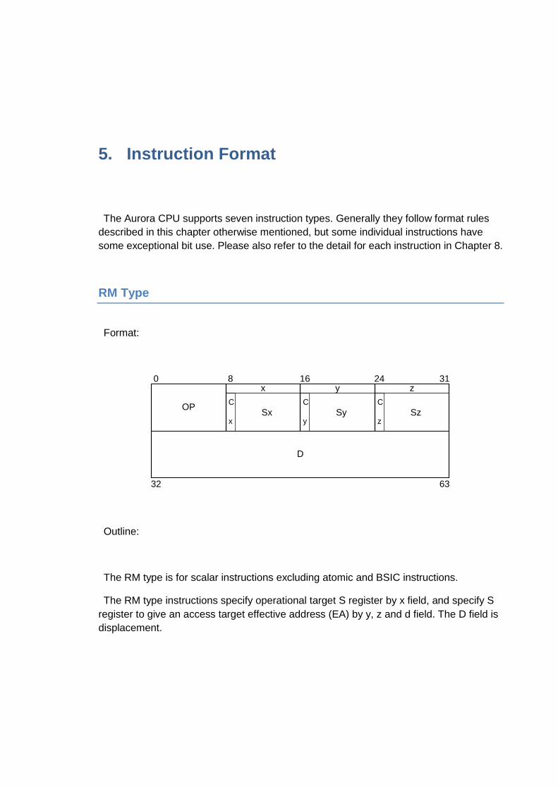
5. Instruction Format
The Aurora CPU supports seven instruction types. Generally they follow format rules
described in this chapter otherwise mentioned, but some individual instructions have
some exceptional bit use. Please also refer to the detail for each instruction in Chapter 8.
RM Type
Format:
x
OP Sx Sy Sz
y
C
y
z
C
z
8 16 24 31
D
32 63
0
C
x
Outline:
The RM type is for scalar instructions excluding atomic and BSIC instructions.
The RM type instructions specify operational target S register by x field, and specify S
register to give an access target effective address (EA) by y, z and d field. The D field is
displacement.
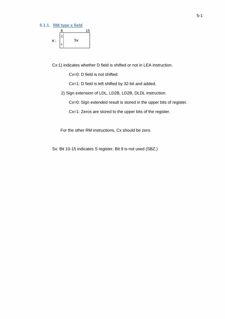
5-1
5.1.1. RM type x field
SxC
x
158
x:
Cx:1) indicates whether D field is shifted or not in LEA instruction.
Cx=0: D field is not shifted.
Cx=1: D field is left shifted by 32-bit and added.
2) Sign extension of LDL, LD2B, LD2B, DLDL instruction.
Cx=0: Sign extended result is stored in the upper bits of register.
Cx=1: Zeros are stored to the upper bits of the register.
For the other RM instructions, Cx should be zero.
Sx: Bit 10-15 indicates S register. Bit 9 is not used (SBZ.)
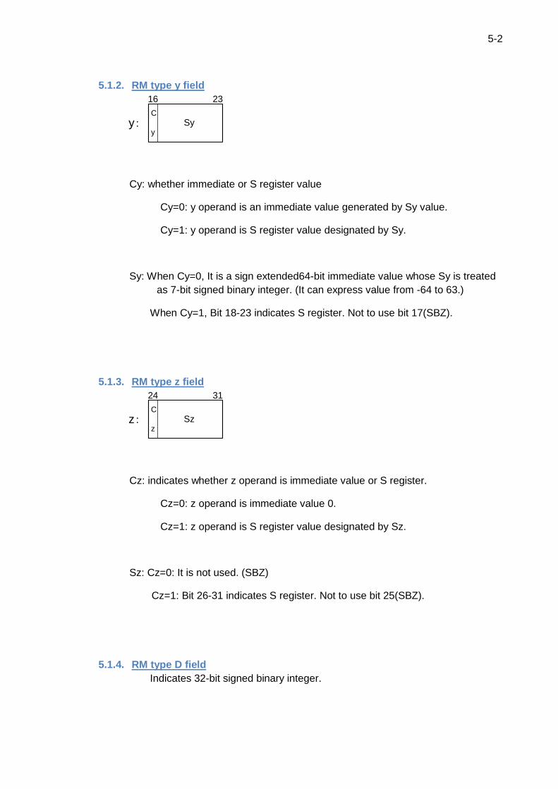
5-2
5.1.2. RM type y field
SyC
y
16 23
y:
Cy: whether immediate or S register value
Cy=0: y operand is an immediate value generated by Sy value.
Cy=1: y operand is S register value designated by Sy.
Sy: When Cy=0, It is a sign extended64-bit immediate value whose Sy is treated
as 7-bit signed binary integer. (It can express value from -64 to 63.)
When Cy=1, Bit 18-23 indicates S register. Not to use bit 17(SBZ).
5.1.3. RM type z field
SzC
z
24 31
z:
Cz: indicates whether z operand is immediate value or S register.
Cz=0: z operand is immediate value 0.
Cz=1: z operand is S register value designated by Sz.
Sz: Cz=0: It is not used. (SBZ)
Cz=1: Bit 26-31 indicates S register. Not to use bit 25(SBZ).
5.1.4. RM type D field
Indicates 32-bit signed binary integer.
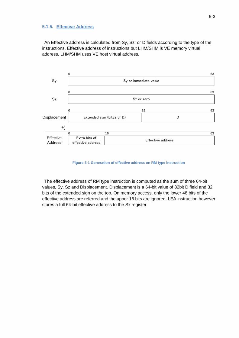
5-3
5.1.5. Effective Address
An Effective address is calculated from Sy, Sz, or D fields according to the type of the
instructions. Effective address of instructions but LHM/SHM is VE memory virtual
address. LHM/SHM uses VE host virtual address.
Figure 5-1 Generation of effective address on RM type instruction
The effective address of RM type instruction is computed as the sum of three 64-bit
values, Sy, Sz and Displacement. Displacement is a 64-bit value of 32bit D field and 32
bits of the extended sign on the top. On memory access, only the lower 48 bits of the
effective address are referred and the upper 16 bits are ignored. LEA instruction however
stores a full 64-bit effective address to the Sx register.
Sy or immediate value
630
Sy
Extended sign (bit32 of D)
Sz or zero
630
Sz
630
Displacement
630
Effective address
+)
32
16
D
Extra bits of effective address
Effective
Address
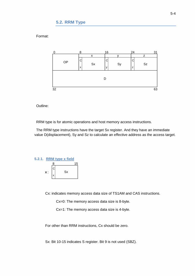
5-4
5.2. RRM Type
Format:
x
OP Sx Sy Sz
y
C
y
z
C
z
8 16 24 31
D
32 63
0
C
x
Outline:
RRM type is for atomic operations and host memory access instructions.
The RRM type instructions have the target Sx register. And they have an immediate
value D(displacement), Sy and Sz to calculate an effective address as the access target.
5.2.1. RRM type x field
SxC
x
158
x:
Cx: indicates memory access data size of TS1AM and CAS instructions.
Cx=0: The memory access data size is 8-byte.
Cx=1: The memory access data size is 4-byte.
For other than RRM instructions, Cx should be zero.
Sx: Bit 10-15 indicates S register. Bit 9 is not used (SBZ).
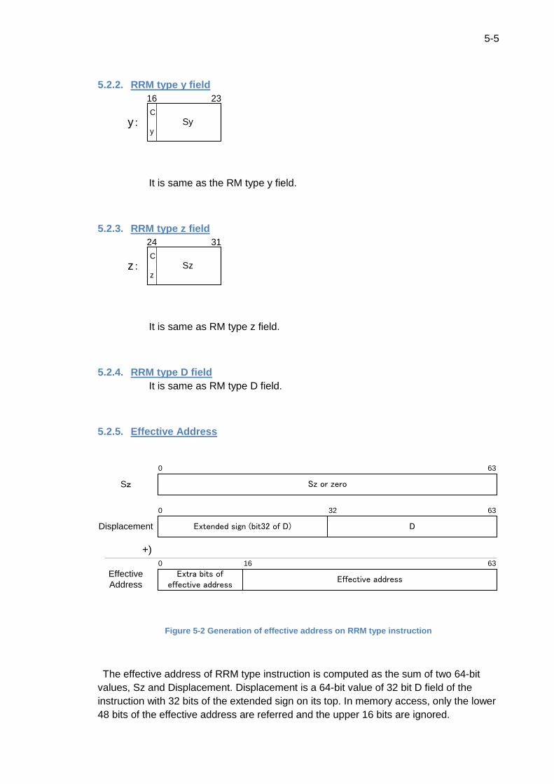
5-5
5.2.2. RRM type y field
SyC
y
16 23
y:
It is same as the RM type y field.
5.2.3. RRM type z field
SzC
z
24 31
z:
It is same as RM type z field.
5.2.4. RRM type D field
It is same as RM type D field.
5.2.5. Effective Address
Figure 5-2 Generation of effective address on RRM type instruction
The effective address of RRM type instruction is computed as the sum of two 64-bit
values, Sz and Displacement. Displacement is a 64-bit value of 32 bit D field of the
instruction with 32 bits of the extended sign on its top. In memory access, only the lower
48 bits of the effective address are referred and the upper 16 bits are ignored.
Extended sign (bit32 of D)
Sz or zero
630
Sz
630
Displacement
630
Effective address
+)
32
16
D
Extra bits of effective address
Effective
Address
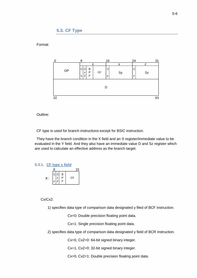
5-6
5.3. CF Type
Format:
x
OP Sy Sz
y
C
y
z
C
z
8 16 24 31
D
32 63
0
C
x
C
x
2
B
P
F
CF
Outline:
CF type is used for branch instructions except for BSIC instruction.
They have the branch condition in the X field and an S register/immediate value to be
evaluated in the Y field. And they also have an immediate value D and Sz register which
are used to calculate an effective address as the branch target.
5.3.1. CF type x field
C
x
C
x
2
B
P
F
CFx:
158
Cx/Cx2:
1) specifies data type of comparison data designated y filed of BCF instruction.
Cx=0: Double precision floating point data.
Cx=1: Single precision floating point data.
2) specifies data type of comparison data designated y field of BCR instruction.
Cx=0, Cx2=0: 64-bit signed binary integer.
Cx=1, Cx2=0: 32-bit signed binary integer.
Cx=0, Cx2=1: Double precision floating point data.
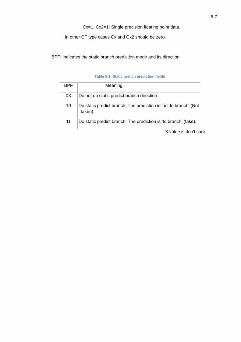
5-7
Cx=1, Cx2=1: Single precision floating point data.
In other CF type cases Cx and Cx2 should be zero.
BPF: indicates the static branch prediction mode and its direction.
Table 5-1: Static branch prediction fields
BPF Meaning
0X Do not do static predict branch direction
10 Do static predict branch. The prediction is ‘not to branch’ (Not
taken).
11 Do static predict branch. The prediction is ‘to branch’ (take).
X:value is don't care
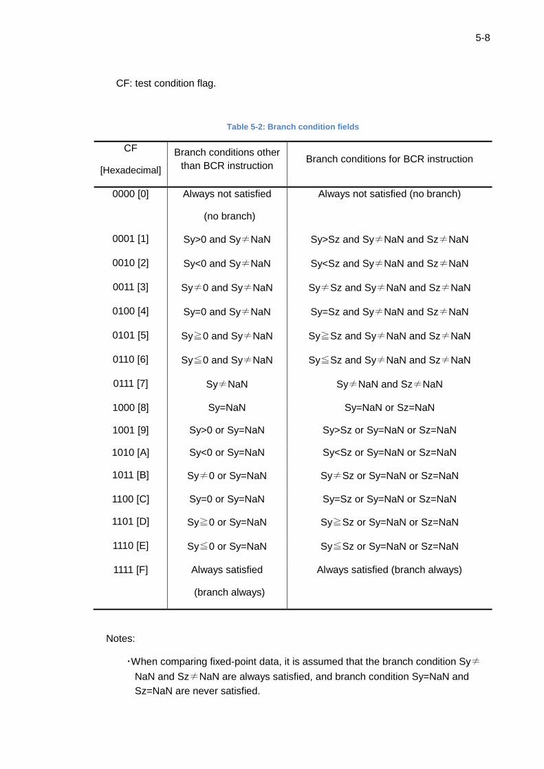
5-8
CF: test condition flag.
Table 5-2: Branch condition fields
CF
[Hexadecimal]
Branch conditions other
than BCR instruction Branch conditions for BCR instruction
0000 [0] Always not satisfied
(no branch)
Always not satisfied (no branch)
0001 [1] Sy>0 and Sy≠NaN Sy>Sz and Sy≠NaN and Sz≠NaN
0010 [2] Sy<0 and Sy≠NaN Sy<Sz and Sy≠NaN and Sz≠NaN
0011 [3] Sy≠0 and Sy≠NaN Sy≠Sz and Sy≠NaN and Sz≠NaN
0100 [4] Sy=0 and Sy≠NaN Sy=Sz and Sy≠NaN and Sz≠NaN
0101 [5] Sy≧0 and Sy≠NaN Sy≧Sz and Sy≠NaN and Sz≠NaN
0110 [6] Sy≦0 and Sy≠NaN Sy≦Sz and Sy≠NaN and Sz≠NaN
0111 [7] Sy≠NaN Sy≠NaN and Sz≠NaN
1000 [8] Sy=NaN Sy=NaN or Sz=NaN
1001 [9] Sy>0 or Sy=NaN Sy>Sz or Sy=NaN or Sz=NaN
1010 [A] Sy<0 or Sy=NaN Sy<Sz or Sy=NaN or Sz=NaN
1011 [B] Sy≠0 or Sy=NaN Sy≠Sz or Sy=NaN or Sz=NaN
1100 [C] Sy=0 or Sy=NaN Sy=Sz or Sy=NaN or Sz=NaN
1101 [D] Sy≧0 or Sy=NaN Sy≧Sz or Sy=NaN or Sz=NaN
1110 [E] Sy≦0 or Sy=NaN Sy≦Sz or Sy=NaN or Sz=NaN
1111 [F] Always satisfied
(branch always)
Always satisfied (branch always)
Notes:
・When comparing fixed-point data, it is assumed that the branch condition Sy≠
NaN and Sz≠NaN are always satisfied, and branch condition Sy=NaN and
Sz=NaN are never satisfied.
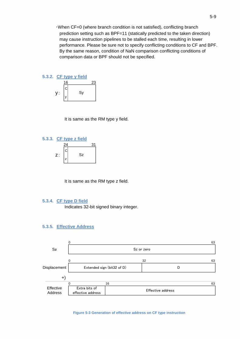
5-9
・When CF=0 (where branch condition is not satisfied), conflicting branch
prediction setting such as BPF=11 (statically predicted to the taken direction)
may cause instruction pipelines to be stalled each time, resulting in lower
performance. Please be sure not to specify conflicting conditions to CF and BPF.
By the same reason, condition of NaN comparison conflicting conditions of
comparison data or BPF should not be specified.
5.3.2. CF type y field
SyC
y
16 23
y:
It is same as the RM type y field.
5.3.3. CF type z field
SzC
z
24 31
z:
It is same as the RM type z field.
5.3.4. CF type D field
Indicates 32-bit signed binary integer.
5.3.5. Effective Address
Figure 5-3 Generation of effective address on CF type instruction
Extended sign (bit32 of D)
Sz or zero
630
Sz
630
Displacement
630
Effective address
+)
32
16
D
Extra bits of effective address
Effective
Address

5-10
The effective address of CF type instructions is computed as the sum of Sz and
displacement. Displacement is a 64-bit value of 32 bit D field of the instruction and 32 bits
of the extended sign on its top. In memory access, only the lower 48 bits of the effective
address are referred and the upper 16 bits are ignored.
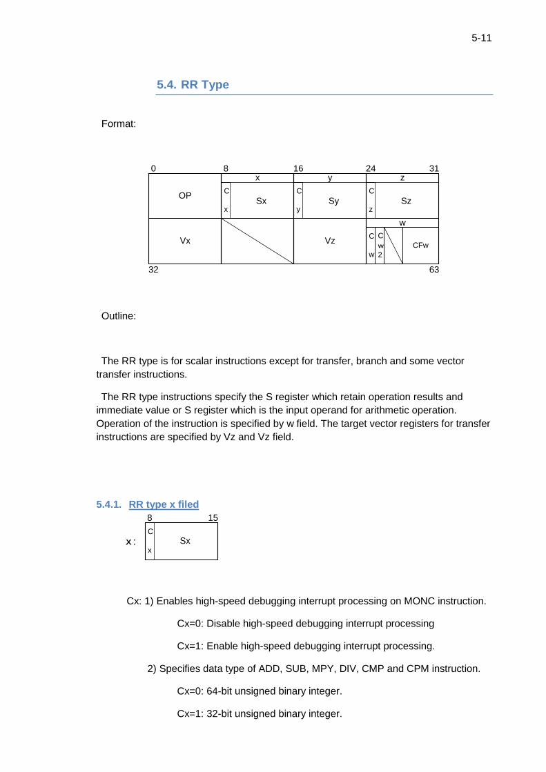
5-11
5.4. RR Type
Format:
x
OP Sx Sy
y
C
y
8 16 24 31
32 63
0
C
x
C
w
Sz
z
C
z
C
w2
CFw
w
Vx Vz
Outline:
The RR type is for scalar instructions except for transfer, branch and some vector
transfer instructions.
The RR type instructions specify the S register which retain operation results and
immediate value or S register which is the input operand for arithmetic operation.
Operation of the instruction is specified by w field. The target vector registers for transfer
instructions are specified by Vz and Vz field.
5.4.1. RR type x filed
SxC
x
158
x:
Cx: 1) Enables high-speed debugging interrupt processing on MONC instruction.
Cx=0: Disable high-speed debugging interrupt processing
Cx=1: Enable high-speed debugging interrupt processing.
2) Specifies data type of ADD, SUB, MPY, DIV, CMP and CPM instruction.
Cx=0: 64-bit unsigned binary integer.
Cx=1: 32-bit unsigned binary integer.
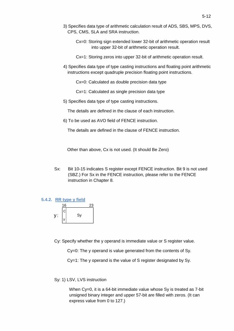
5-12
3) Specifies data type of arithmetic calculation result of ADS, SBS, MPS, DVS,
CPS, CMS, SLA and SRA instruction.
Cx=0: Storing sign extended lower 32-bit of arithmetic operation result
into upper 32-bit of arithmetic operation result.
Cx=1: Storing zeros into upper 32-bit of arithmetic operation result.
4) Specifies data type of type casting instructions and floating point arithmetic
instructions except quadruple precision floating point instructions.
Cx=0: Calculated as double precision data type
Cx=1: Calculated as single precision data type
5) Specifies data type of type casting instructions.
The details are defined in the clause of each instruction.
6) To be used as AVO field of FENCE instruction.
The details are defined in the clause of FENCE instruction.
Other than above, Cx is not used. (It should Be Zero)
Sx: Bit 10-15 indicates S register except FENCE instruction. Bit 9 is not used
(SBZ.) For Sx in the FENCE instruction, please refer to the FENCE
instruction in Chapter 8.
5.4.2. RR type y field
SyC
y
16 23
y:
Cy: Specify whether the y operand is immediate value or S register value.
Cy=0: The y operand is value generated from the contents of Sy.
Cy=1: The y operand is the value of S register designated by Sy.
Sy: 1) LSV, LVS instruction
When Cy=0, it is a 64-bit immediate value whose Sy is treated as 7-bit
unsigned binary integer and upper 57-bit are filled with zeros. (It can
express value from 0 to 127.)
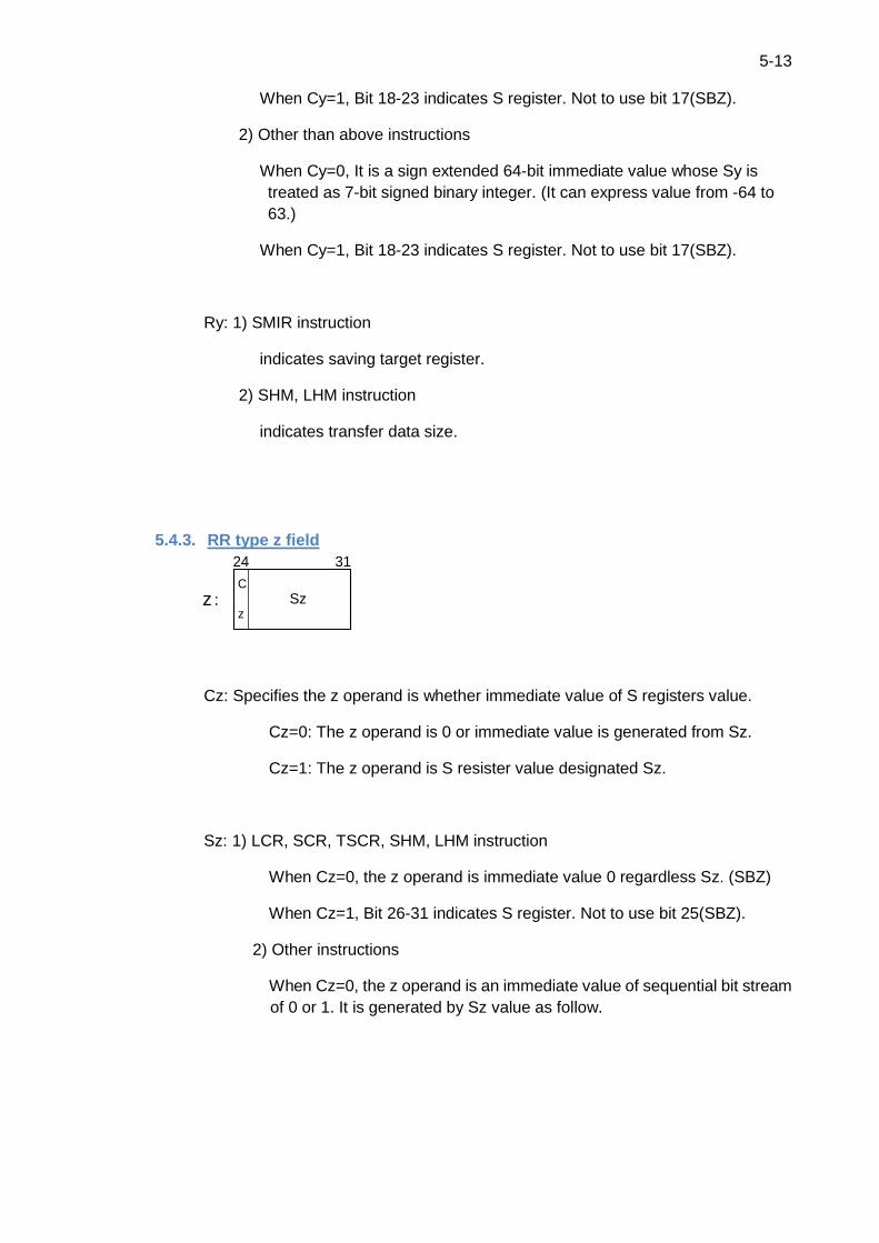
5-13
When Cy=1, Bit 18-23 indicates S register. Not to use bit 17(SBZ).
2) Other than above instructions
When Cy=0, It is a sign extended 64-bit immediate value whose Sy is
treated as 7-bit signed binary integer. (It can express value from -64 to
63.)
When Cy=1, Bit 18-23 indicates S register. Not to use bit 17(SBZ).
Ry: 1) SMIR instruction
indicates saving target register.
2) SHM, LHM instruction
indicates transfer data size.
5.4.3. RR type z field
SzC
z
24 31
z:
Cz: Specifies the z operand is whether immediate value of S registers value.
Cz=0: The z operand is 0 or immediate value is generated from Sz.
Cz=1: The z operand is S resister value designated Sz.
Sz: 1) LCR, SCR, TSCR, SHM, LHM instruction
When Cz=0, the z operand is immediate value 0 regardless Sz. (SBZ)
When Cz=1, Bit 26-31 indicates S register. Not to use bit 25(SBZ).
2) Other instructions
When Cz=0, the z operand is an immediate value of sequential bit stream
of 0 or 1. It is generated by Sz value as follow.
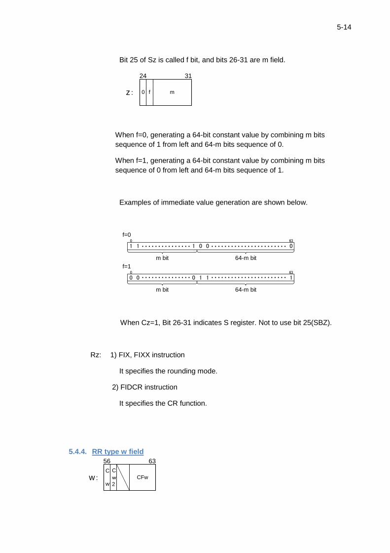
5-14
Bit 25 of Sz is called f bit, and bits 26-31 are m field.
0
24 31
z: f m
When f=0, generating a 64-bit constant value by combining m bits
sequence of 1 from left and 64-m bits sequence of 0.
When f=1, generating a 64-bit constant value by combining m bits
sequence of 0 from left and 64-m bits sequence of 1.
Examples of immediate value generation are shown below.
1 1 1 0 0 0
m bit 64-m bit
0 0 0 1 1 1
m bit 64-m bit
f=0
f=1
0 63
0 63
When Cz=1, Bit 26-31 indicates S register. Not to use bit 25(SBZ).
Rz: 1) FIX, FIXX instruction
It specifies the rounding mode.
2) FIDCR instruction
It specifies the CR function.
5.4.4. RR type w field
56 63
w:C
w
C
w2
CFw
5-15
Cw/Cw2: 1) Specifies comparison criteria of CMS, CMX and FCM instruction.
Cw=0: larger value.
Cw=1: smaller value.
2) Specifies data type of CMOV instruction.
Cw=0, Cw2=0: 64-bit signed binary integer.
Cw=1, Cw2=0: 32-bit signed binary integer.
Cw=0, Cw2=1: double precision floating point data.
Cw=1, Cw2=1: single precision floating point data
3) Specifies data type of FIX instruction operation result.
Cw=0: Storing sign extended lower 32-bit of arithmetic operation
result into upper 32-bit of arithmetic operation result.
Cw=1: Storing zeros into upper 32-bit of arithmetic operation result.
CFw: Specifies comparison criteria of CMOV instruction.
The condition is the same as the CF type X field.
5.4.5. RR type Vx and Vz field
They are vector register or vector mask register for vector transfer instructions.
When used as a vector register, the register is expressed by lower 6 bits of
the field. The upper 2 bits are not used (SBZ).
When Vx=255 is assigned in Vx field, the vector register designated by VIXR
is exceptionally taken as the target of the transfer. Similarly, Vz=255 also
indicates VIXR indirect access for the operand Vz register.
5-16
5.5. RW Type
Format:
x
OP Sx Sy Sz
y
C
y
z
C
z
8 16 24 31
32 63
0
C
x
Outline:
The RW type is for arithmetic instructions whose input operand is quadratic precision
floating point data type.
The RW type instructions are the same as RR type instructions except the followings.
The RW type instructions, when the I/O operands are quadratic precision floating point
data, a S register pair can be indicated in x, y and z field. The S register pair is
combination of even number S register and its sequential odd number S register. In the
other words, the odd number is equal to the even number plus 1.
The instructions which indicate S register pair by x field are FAQ, FSQ, FMQ and CVQ
instruction.
The instructions which indicate S register pair by y field are FAQ, FSQ, FMQ, FCQ,
CVD (in case Cx=1) and CVS (in case Cx=1) instruction.
The instructions which indicate S register pair by z field are FAQ, FSQ, FMQ and FCQ
instruction.
If an odd number S register is indicated in the above instructions x, y and z field, then an
illegal instruction format exception is generated.
5-17
The instructions which indicate S register pair by y or z field, Cy and Cz should be ‘1’.
But if 0 is indicated (i.e. immediate value is indicated) then an immediate value which is
explained RR type chapter is generated and use it as input operand. In this case the
immediate value corresponding y field odd number register will be the value which is
indicated by immediate filed plus 1, and the immediate value corresponding z field odd
number register will be generated by reversing the bit 31 of the instruction.
5-18
5.6. RVM Type
Format:
x
OP Sy Sz
y
C
y
z
C
z
8 16 24 31
32 63
0
C
x
/
V
O
Vx Vy
V
C
M
C
s
Sw
w
Outline:
The RVM type is for vector transfer instructions.
The RVM type instructions specify transfer control flags and vector mask registers by x
field, S registers which designate source and destination address by y and z field, S
registers which designate vector register number for storing list address by w field,
source and destination vector register by Vx field and vector registers which retain list
address by Vy field.
5.6.1. RVM type x field
158
x:
C
x
/
V
O
V
C
M
C
s
Cx: indicates whether sign extension is applied or not on VLDL, VLDL2D and VGTL
instruction.
Cx=0: Sign extended load data is stored into upper bit of register.
Cx=1: Upper bit of register are filled with zeros.
VO: For VST, VSTU, VSTL, VST2D, VSTU2D, VSTL2D, VSC, VSCU and VSCL
instruction, specify how to guarantee operation order for address
dependence with following load instructions.
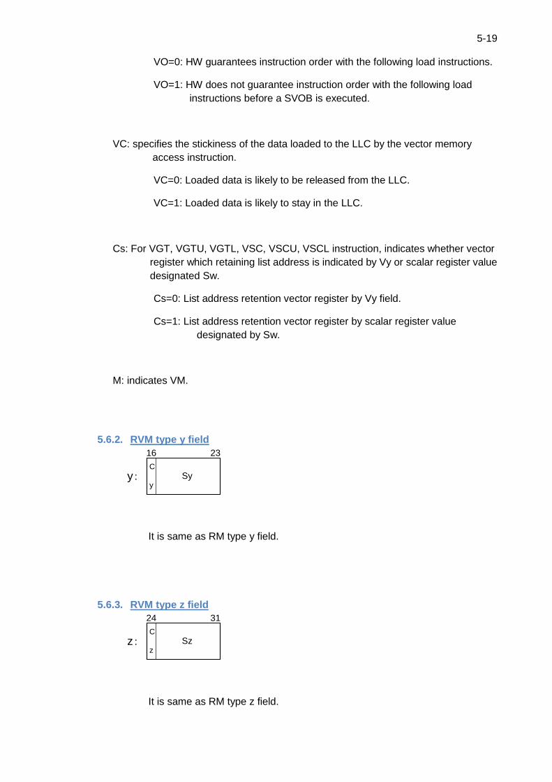
5-19
VO=0: HW guarantees instruction order with the following load instructions.
VO=1: HW does not guarantee instruction order with the following load
instructions before a SVOB is executed.
VC: specifies the stickiness of the data loaded to the LLC by the vector memory
access instruction.
VC=0: Loaded data is likely to be released from the LLC.
VC=1: Loaded data is likely to stay in the LLC.
Cs: For VGT, VGTU, VGTL, VSC, VSCU, VSCL instruction, indicates whether vector
register which retaining list address is indicated by Vy or scalar register value
designated Sw.
Cs=0: List address retention vector register by Vy field.
Cs=1: List address retention vector register by scalar register value
designated by Sw.
M: indicates VM.
5.6.2. RVM type y field
SyC
y
16 23
y:
It is same as RM type y field.
5.6.3. RVM type z field
SzC
z
24 31
z:
It is same as RM type z field.
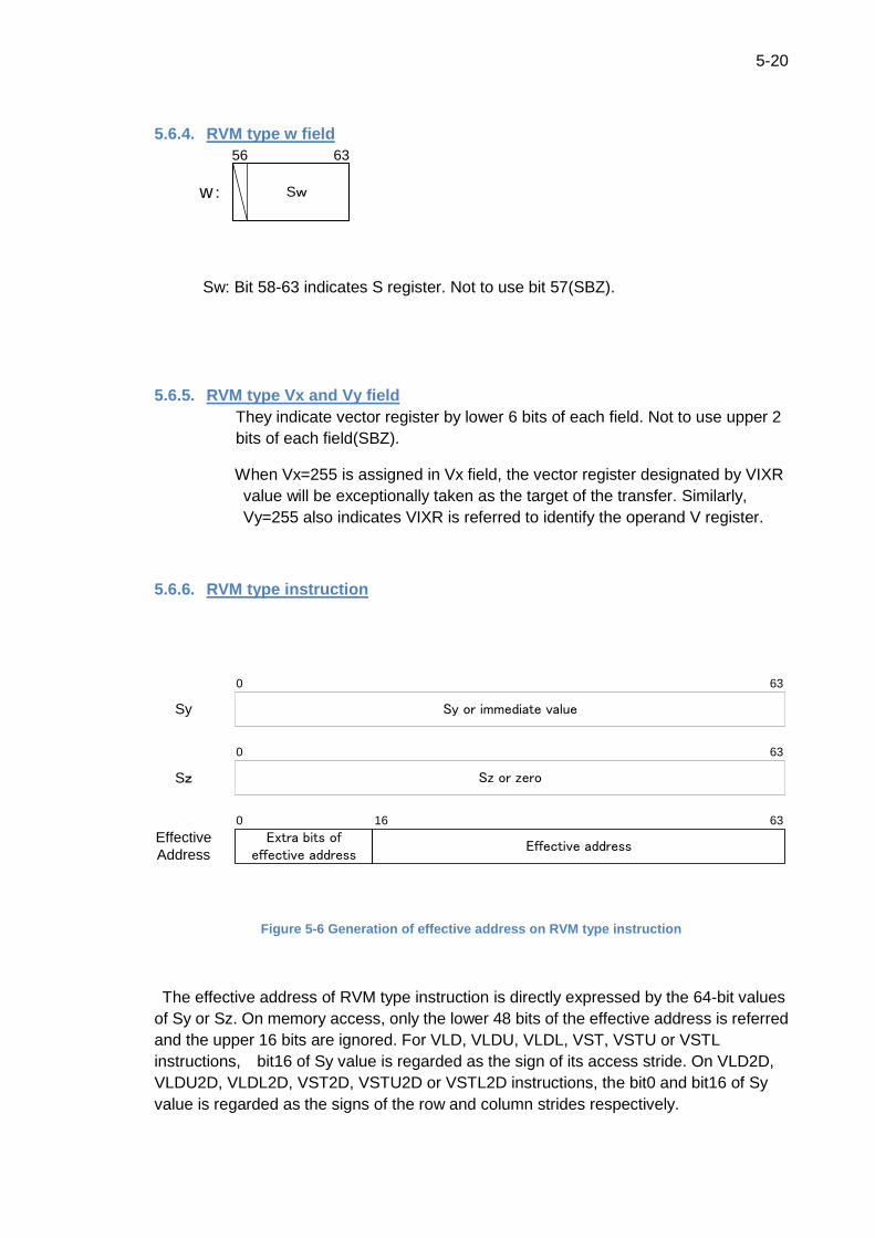
5-20
5.6.4. RVM type w field
56 63
w: Sw
Sw: Bit 58-63 indicates S register. Not to use bit 57(SBZ).
5.6.5. RVM type Vx and Vy field
They indicate vector register by lower 6 bits of each field. Not to use upper 2
bits of each field(SBZ).
When Vx=255 is assigned in Vx field, the vector register designated by VIXR
value will be exceptionally taken as the target of the transfer. Similarly,
Vy=255 also indicates VIXR is referred to identify the operand V register.
5.6.6. RVM type instruction
Figure 5-6 Generation of effective address on RVM type instruction
The effective address of RVM type instruction is directly expressed by the 64-bit values
of Sy or Sz. On memory access, only the lower 48 bits of the effective address is referred
and the upper 16 bits are ignored. For VLD, VLDU, VLDL, VST, VSTU or VSTL
instructions, bit16 of Sy value is regarded as the sign of its access stride. On VLD2D,
VLDU2D, VLDL2D, VST2D, VSTU2D or VSTL2D instructions, the bit0 and bit16 of Sy
value is regarded as the signs of the row and column strides respectively.
Sy or immediate value
630
Sy
Sz or zero
630
Sz
630
Effective address
16
Extra bits of effective address
Effective
Address
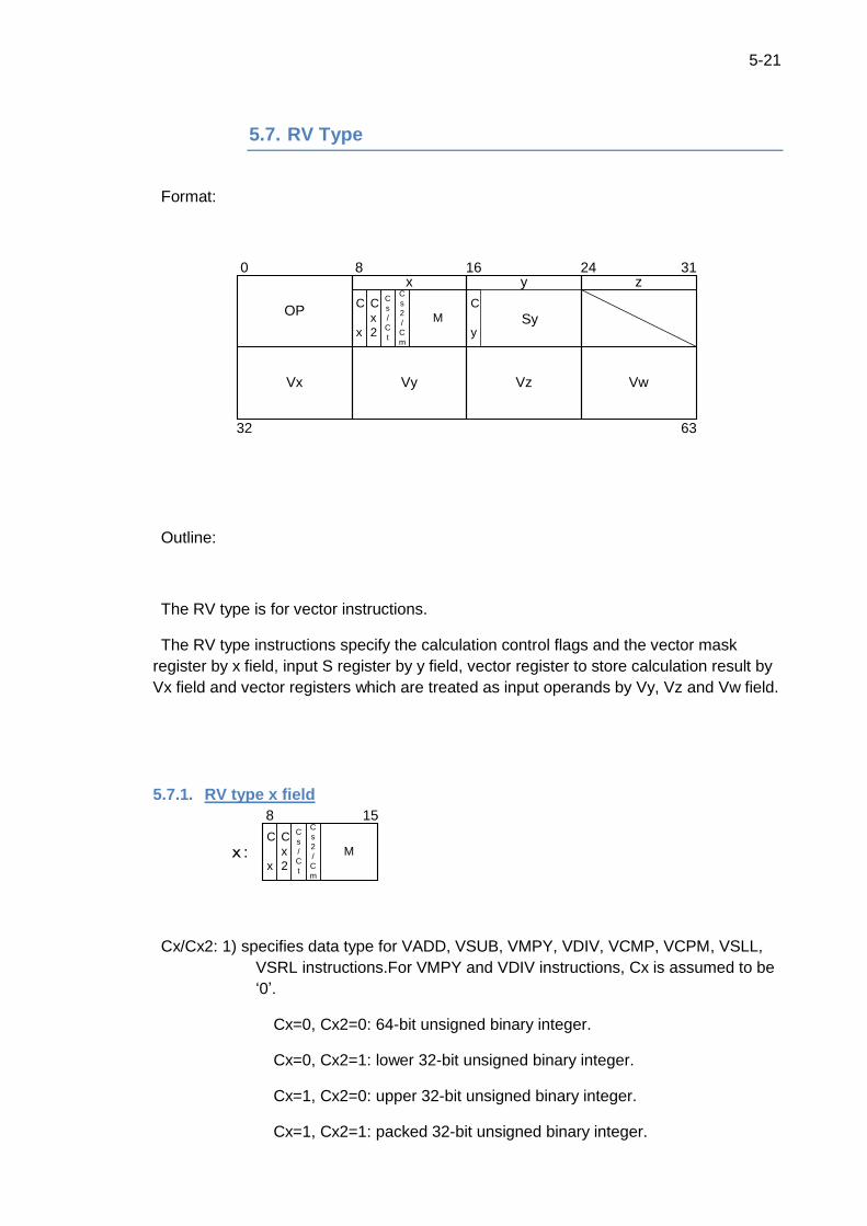
5-21
5.7. RV Type
Format:
8 16 24 31
32 63
0x
OP Sy
y
C
y
z
Vx Vy
C
x
2
M
C
s
/
C
t
C
x
C
s
2
/
C
m
Vz Vw
Outline:
The RV type is for vector instructions.
The RV type instructions specify the calculation control flags and the vector mask
register by x field, input S register by y field, vector register to store calculation result by
Vx field and vector registers which are treated as input operands by Vy, Vz and Vw field.
5.7.1. RV type x field
158
x: M
C
x
2
C
s
/
C
t
C
x
C
s
2
/
C
m
Cx/Cx2: 1) specifies data type for VADD, VSUB, VMPY, VDIV, VCMP, VCPM, VSLL,
VSRL instructions.For VMPY and VDIV instructions, Cx is assumed to be
‘0’.
Cx=0, Cx2=0: 64-bit unsigned binary integer.
Cx=0, Cx2=1: lower 32-bit unsigned binary integer.
Cx=1, Cx2=0: upper 32-bit unsigned binary integer.
Cx=1, Cx2=1: packed 32-bit unsigned binary integer.
5-22
2) specifies data type for VADS, VSBS, VMPS, VDVS, VCPS, VCMS, VSUMS,
VMAXS, VSLA, VSRA instructions. For VMPS, VDVS, VSUMS, VMAXS
instructions, Cx is assumed to be ‘0’.
Cx=0, Cx2=0: lower 32-bit signed binary integer with sign extention.
Cx=0, Cx2=1: lower 32-bit signed binary integer without sign extention.
Cx=1, Cx2=0: upper 32-bit signed binary integer.
Cx=1, Cx2=1: packed 32-bit signed binary integer.
3) specifies data type for vector floating point arithmetic instructions. For the
instructions which do not have packed data operating function, Cx2 is
assumed to be ‘0’
Cx=0, Cx2=0: double precision floating point data.
Cx=0, Cx2=1: lower 32-bit single precision floating point data.
Cx=1, Cx2=0: upper 32-bit single precision floating point data.
Cx=1, Cx2=1: packed 32-bit single precision floating point data.
4) specifies data type for VFIX and VFLT instructions.
For details, see chapter 8.
5-23
5) specifies data type for VBRD, VAND, VOR, VXOR, VEQV, VLDZ, VPCNT,
VBRV, VSEQ instructions.
Cx=0, Cx2=0: 64-bit logical data.
Cx=0, Cx2=1: lower 32-bit logical data.
Cx=1, Cx2=0: upper 32-bit logical data.
Cx=1, Cx2=1: packed 32-bit logical data.
6) specifies data type for VMRG instruction.
Cx=0: 64-bit logical data.
Cx=1: packed 32-bit logical data
7) specifies data type for VFMS instruction.
Cx=0: lower 32-bit signed binary integer
Cx=1: upper 32-bit signed binary integer
8) specifies data type for VFMF instruction.
Cx=0, Cx2=0: double precision floating point data.
Cx=0, Cx2=1: lower 32-bit single precision floating point data.
Cx=1, Cx2=0: upper 32-bit single precision floating point data.
Ct: Specifies how to select the element number of maximum and minimum value
in case that several elements are the same maximum or minimum value.
Ct=0: Store the smaller element number as a result.
Ct=1: Store the bigger element number as a result.
Cm: 1) specifies comparison conditions of VCMS, VCMX, VFCM instructions.
Cm=0: selects the bigger value.
Cm=1: selects the smaller value.
2) specifies operation of VRSQRT instruction when 0 is inputted.
Cm=0: When 0 is inputted, a divide exception is generated.
Cm=1: When 0 is inputted, a divide exception is NOT generated.
3) Specifies data type of VFIX and VFLT instructions.
5-24
Cm=0: Non-packed data type.
Cm=1: Packed data type.
4) Specifies comparison conditions of VMAXS, VMAXX, VFMAX instructions.
Cm=0: Find the maximum value of vector elements.
Cm=1: Find the minimum value of vector elements.
Cs/Cs2:1) Specifies Vy and Vz operand of VDIV, VDVS, VDVX, VFDV, VFMAD,
VFMSB, VFNMAD, VFNMSB instructions.
Cs=0, Cs2=0: Sy value is not used.
Cs=1, Cs2=0: Specifies immediate value or S register value designated
Sy as input operand replace with Vy.
Cs=0, Cs2=1: Specifies immediate value or S register value designated
Sy as input operand replace with Vz.
Cs=1, Cs2=1: Unspecified behavior. If it is assigned, then an illegal
instruction format exception is generated.
2) Specifies Vy operand of other than above vector arithmetic instructions.
Cs=0: Sy value is not used.
Cs=1: Specifies immediate value or S register value designated Sy as
input operand replace with Vy.
M: Specifies a VM.
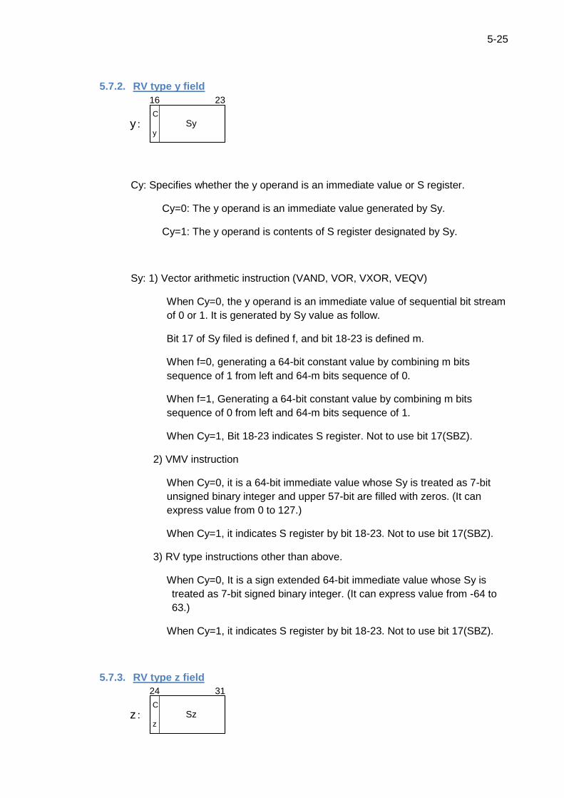
5-25
5.7.2. RV type y field
SyC
y
16 23
y:
Cy: Specifies whether the y operand is an immediate value or S register.
Cy=0: The y operand is an immediate value generated by Sy.
Cy=1: The y operand is contents of S register designated by Sy.
Sy: 1) Vector arithmetic instruction (VAND, VOR, VXOR, VEQV)
When Cy=0, the y operand is an immediate value of sequential bit stream
of 0 or 1. It is generated by Sy value as follow.
Bit 17 of Sy filed is defined f, and bit 18-23 is defined m.
When f=0, generating a 64-bit constant value by combining m bits
sequence of 1 from left and 64-m bits sequence of 0.
When f=1, Generating a 64-bit constant value by combining m bits
sequence of 0 from left and 64-m bits sequence of 1.
When Cy=1, Bit 18-23 indicates S register. Not to use bit 17(SBZ).
2) VMV instruction
When Cy=0, it is a 64-bit immediate value whose Sy is treated as 7-bit
unsigned binary integer and upper 57-bit are filled with zeros. (It can
express value from 0 to 127.)
When Cy=1, it indicates S register by bit 18-23. Not to use bit 17(SBZ).
3) RV type instructions other than above.
When Cy=0, It is a sign extended 64-bit immediate value whose Sy is
treated as 7-bit signed binary integer. (It can express value from -64 to
63.)
When Cy=1, it indicates S register by bit 18-23. Not to use bit 17(SBZ).
5.7.3. RV type z field
SzC
z
24 31
z:
5-26
Cz: Specifies whether the z operand is an immediate value or S register.
Cz=0: The y operand is an immediate value generated by Sz.
Cz=1: The y operand is contents of S register designated by Sz.
Sz: When Cz=0, the z operand is an immediate value of sequential bit stream of 0
or 1. It is generated by Sz value as follow.
Bit 25 of Sz filed is defined f, and bit 26-31 is defined m.
When f=0, generating a 64-bit constant value by combining m bits sequence
of 1 from left and 64-m bits sequence of 0.
When f=1, Generating a 64-bit constant value by combining m bits sequence
of 0 from left and 64-m bits sequence of 1.
When Cz=1, Bit 26-31 indicates S register. Not to use bit 25(SBZ).
5.7.4. RV type Vx, Vy, Vz, Vw field
Generally they specify vector registers or vector mask registers.
When they specify vector registers, the vector register is determined by lower
6 bits of each field unless those fields are 255. In this case, upper 2 bits of
each field are ignored (SBZ). When 255 is specified, the vector register is
determined by the value in the VIXR.
On VFIX or VFIXX instruction, rounding condition is specified by lower 4 bits
of the Vz field.
On VFMK, VFMS, or VFMF instruction, evaluation condition is specified by
lower 4 bits of the Vy field. The interpretation of evaluation condition is the
same as CF type x filed.
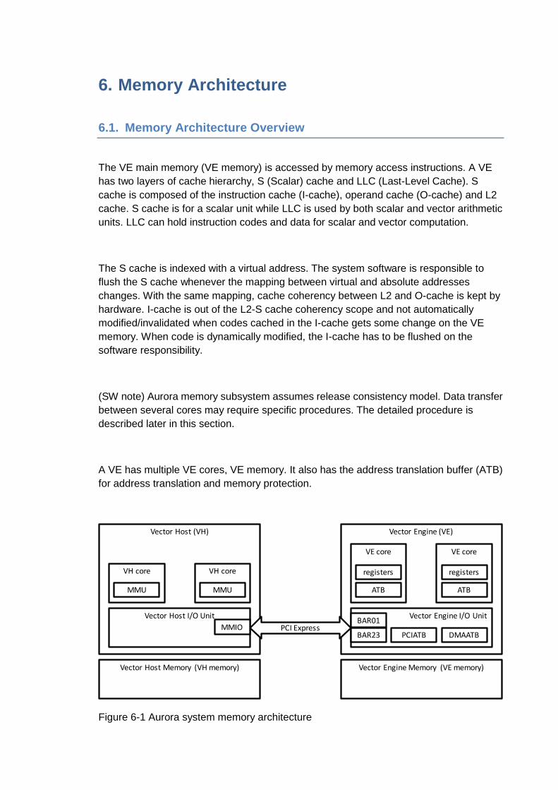
6. Memory Architecture
6.1. Memory Architecture Overview
The VE main memory (VE memory) is accessed by memory access instructions. A VE
has two layers of cache hierarchy, S (Scalar) cache and LLC (Last-Level Cache). S
cache is composed of the instruction cache (I-cache), operand cache (O-cache) and L2
cache. S cache is for a scalar unit while LLC is used by both scalar and vector arithmetic
units. LLC can hold instruction codes and data for scalar and vector computation.
The S cache is indexed with a virtual address. The system software is responsible to
flush the S cache whenever the mapping between virtual and absolute addresses
changes. With the same mapping, cache coherency between L2 and O-cache is kept by
hardware. I-cache is out of the L2-S cache coherency scope and not automatically
modified/invalidated when codes cached in the I-cache gets some change on the VE
memory. When code is dynamically modified, the I-cache has to be flushed on the
software responsibility.
(SW note) Aurora memory subsystem assumes release consistency model. Data transfer
between several cores may require specific procedures. The detailed procedure is
described later in this section.
A VE has multiple VE cores, VE memory. It also has the address translation buffer (ATB)
for address translation and memory protection.
Figure 6-1 Aurora system memory architecture
Vector Host (VH)
VH core
MMU
Vector Host Memory (VH memory)
Vector Engine (VE)
VE core
ATB
Vector Engine Memory (VE memory)
VE core
ATB
Vector Host I/O Unit
VH core
MMU
Vector Engine I/O Unit
DMAATBPCIATB
registers registers
PCI ExpressMMIOBAR01
BAR23
6-1
6.2. Address Space
Virtual addresses of the VE memory are translated into absolute addresses by ATB
(Address Translation Buffer).
VE memory virtual address space
The VE memory virtual address space is used for memory access from a VE core. Each
VE core can have its own VE memory virtual address space. All memory access
instructions except LHM and SHM, and instruction fetch are processed within this
address space. VE memory virtual address is translated to a VE memory absolute
address space through ATB. This address space is 48 bit addressable.
VE host virtual address space
The VE host virtual address space is for DMA or LHM/SHM from a VE core. A VE host
virtual address is translated to a VE memory absolute address, VE register absolute
address, VE CR absolute address or VH system absolute address. This address space is
48 bit addressable.
VH virtual address space
The VH virtual address space is used by programs running on the VH. The VH virtual
address is translated to the VH system absolute address by the MMU mechanism on the
VH. Details of VH virtual address space or MMU are out of scope of this guidebook.
6.2.1. Absolute address space
VE memory absolute address space
The VE memory absolute address space is for VE main memory. This address space is
48 bit addressable.
VE register absolute address space
6-2
The VE register absolute address space is for registers in a VE node. The user registers,
system protection registers and system common registers are mapped on this address
space. This address space is 48 bit addressable.
Access to VE register absolute address space may produce exceptions depending on its
address and transfer size.
VE CR absolute address space
The VE CR absolute address space is mapped to communication registers in the VE
node. The same CRs have multiple addresses depending on the access type such as
read, write and other atomic operations. The size of this address space is 256KB.
To access a VE CR, its absolute addresses has to be 8B aligned, and its access size has
to be 8 bytes.
VH system absolute address space
6-3
6.3. Types of Memory Access
6.3.1. VE core memory accesses
Instruction fetch
Instruction fetch is one type of memory accesses automatically invoked by VE cores to
load instruction codes from the VE memory/LLC/L2 cache to L1 instruction cache. This
memory access is originated with a VE virtual memory address. When it needs to get
access to LLC/the main memory due to L1/L2 cache miss, the address is translated into
a VE absolute memory address by ATB.
Memory access instructions
Memory access instructions including LDS/STS/VLD/VST etc. in VE’s codes are issued
by a VE core with VE virtual memory addresses. When it needs to get access to LLC/the
main memory due to L1/L2 cache miss, the address is translated into a VE absolute
memory address by ATB.
Host memory access instructions
LHM/SHM instructions are provided to access the host memory with a VE host virtual
address.
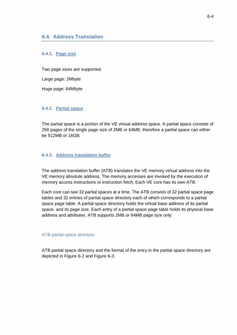
6-4
6.4. Address Translation
6.4.1. Page size
Two page sizes are supported.
Large page: 2Mbyte
Huge page: 64Mbyte
6.4.2. Partial space
The partial space is a portion of the VE virtual address space. A partial space consists of
256 pages of the single page size of 2MB or 64MB, therefore a partial space can either
be 512MB or 16GB.
6.4.3. Address translation buffer
The address translation buffer (ATB) translates the VE memory virtual address into the
VE memory absolute address. The memory accesses are invoked by the execution of
memory access instructions or instruction fetch. Each VE core has its own ATB.
Each core can see 32 partial spaces at a time. The ATB consists of 32 partial space page
tables and 32 entries of partial space directory each of which corresponds to a partial
space page table. A partial space directory holds the virtual base address of its partial
space, and its page size. Each entry of a partial space page table holds its physical base
address and attributes. ATB supports 2MB or 64MB page size only.
ATB partial space directory
ATB partial space directory and the format of the entry in the partial space directory are
depicted in Figure 6-2 and Figure 6-3.
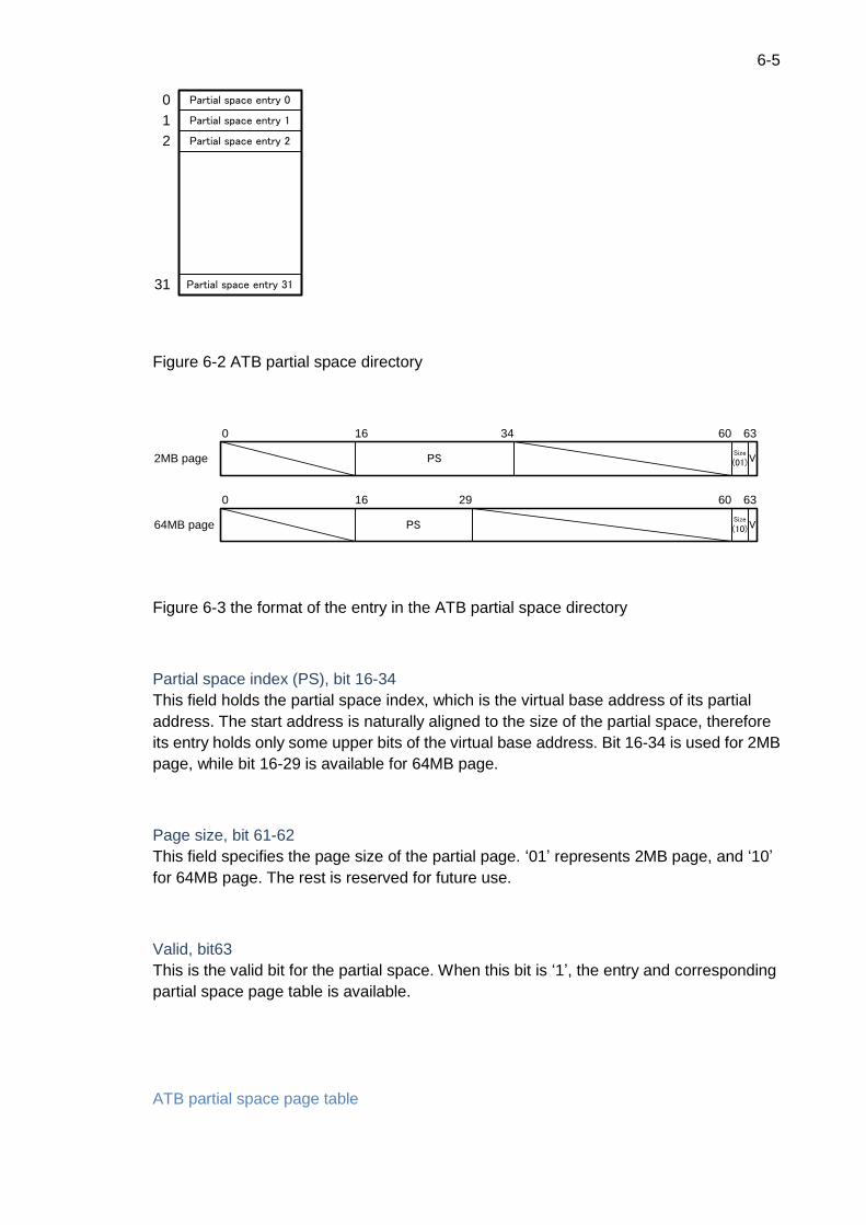
6-5
Figure 6-2 ATB partial space directory
Figure 6-3 the format of the entry in the ATB partial space directory
Partial space index (PS), bit 16-34
This field holds the partial space index, which is the virtual base address of its partial
address. The start address is naturally aligned to the size of the partial space, therefore
its entry holds only some upper bits of the virtual base address. Bit 16-34 is used for 2MB
page, while bit 16-29 is available for 64MB page.
Page size, bit 61-62
This field specifies the page size of the partial page. ‘01’ represents 2MB page, and ‘10’
for 64MB page. The rest is reserved for future use.
Valid, bit63
This is the valid bit for the partial space. When this bit is ‘1’, the entry and corresponding
partial space page table is available.
ATB partial space page table
Partial space entry 31
Partial space entry 0
Partial space entry 1
Partial space entry 2
0
1
2
31
6360160 34
VPSSize
(01)
VPSSize
(10)
2MB page
64MB page
6360160 29
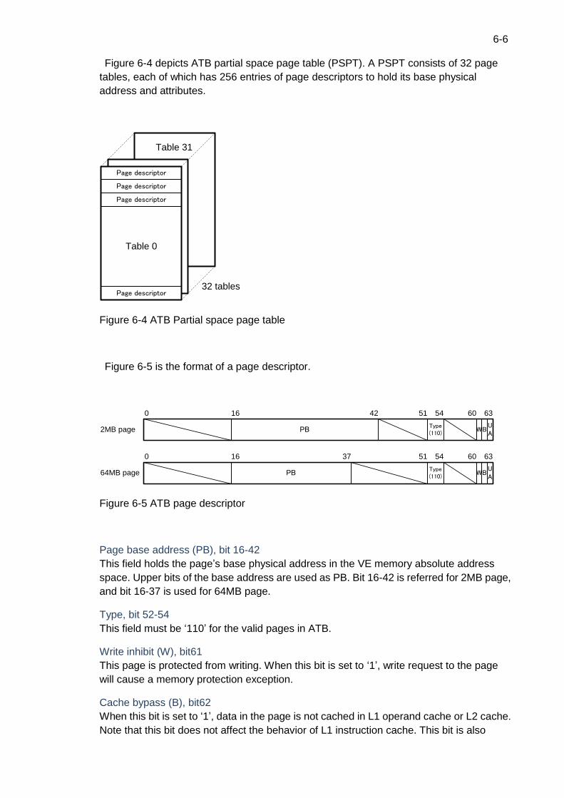
6-6
Figure 6-4 depicts ATB partial space page table (PSPT). A PSPT consists of 32 page
tables, each of which has 256 entries of page descriptors to hold its base physical
address and attributes.
Figure 6-4 ATB Partial space page table
Figure 6-5 is the format of a page descriptor.
Figure 6-5 ATB page descriptor
Page base address (PB), bit 16-42
This field holds the page’s base physical address in the VE memory absolute address
space. Upper bits of the base address are used as PB. Bit 16-42 is referred for 2MB page,
and bit 16-37 is used for 64MB page.
Type, bit 52-54
This field must be ‘110’ for the valid pages in ATB.
Write inhibit (W), bit61
This page is protected from writing. When this bit is set to ‘1’, write request to the page
will cause a memory protection exception.
Cache bypass (B), bit62
When this bit is set to ‘1’, data in the page is not cached in L1 operand cache or L2 cache.
Note that this bit does not affect the behavior of L1 instruction cache. This bit is also
Page descriptor
Page descriptor
Page descriptor
Page descriptor
32 tables
Table 0
Table 31
6360160 42
UA
PB
UA
PB
2MB page
64MB page
6360160 37
Type(110)
BW
Type(110)
BW
51 54
51 54
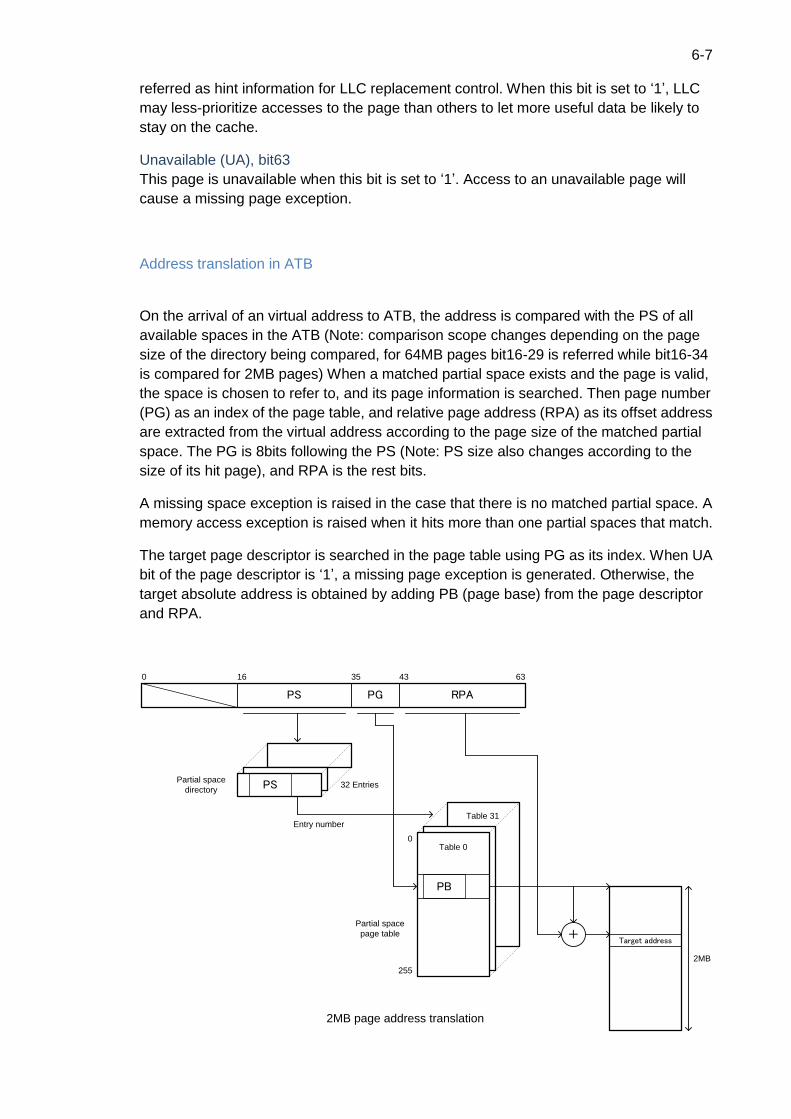
6-7
referred as hint information for LLC replacement control. When this bit is set to ‘1’, LLC
may less-prioritize accesses to the page than others to let more useful data be likely to
stay on the cache.
Unavailable (UA), bit63
This page is unavailable when this bit is set to ‘1’. Access to an unavailable page will
cause a missing page exception.
Address translation in ATB
On the arrival of an virtual address to ATB, the address is compared with the PS of all
available spaces in the ATB (Note: comparison scope changes depending on the page
size of the directory being compared, for 64MB pages bit16-29 is referred while bit16-34
is compared for 2MB pages) When a matched partial space exists and the page is valid,
the space is chosen to refer to, and its page information is searched. Then page number
(PG) as an index of the page table, and relative page address (RPA) as its offset address
are extracted from the virtual address according to the page size of the matched partial
space. The PG is 8bits following the PS (Note: PS size also changes according to the
size of its hit page), and RPA is the rest bits.
A missing space exception is raised in the case that there is no matched partial space. A
memory access exception is raised when it hits more than one partial spaces that match.
The target page descriptor is searched in the page table using PG as its index. When UA
bit of the page descriptor is ‘1’, a missing page exception is generated. Otherwise, the
target absolute address is obtained by adding PB (page base) from the page descriptor
and RPA.
63160 35
RPAPS PG
43
PS
0
255
Table 0
Table 31
PB
Partial space
directory
Partial space
page tableTarget address
+
2MB
Entry number
2MB page address translation
32 Entries
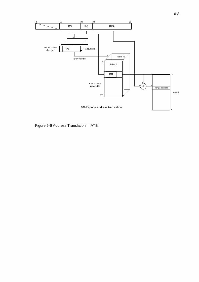
6-8
Figure 6-6 Address Translation in ATB
63160 30
RPAPS PG
38
PS
0
255
Table 0
Table 31
PB
Partial space
directory
Partial space
page tableTarget address
+
64MB
Entry number
64MB page address translation
32 Entries
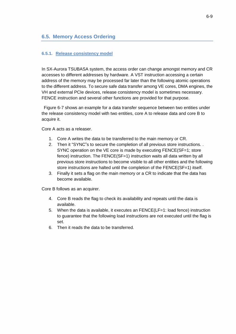
6-9
6.5. Memory Access Ordering
6.5.1. Release consistency model
In SX-Aurora TSUBASA system, the access order can change amongst memory and CR
accesses to different addresses by hardware. A VST instruction accessing a certain
address of the memory may be processed far later than the following atomic operations
to the different address. To secure safe data transfer among VE cores, DMA engines, the
VH and external PCIe devices, release consistency model is sometimes necessary.
FENCE instruction and several other functions are provided for that purpose.
Figure 6-7 shows an example for a data transfer sequence between two entities under
the release consistency model with two entities, core A to release data and core B to
acquire it.
Core A acts as a releaser.
1. Core A writes the data to be transferred to the main memory or CR.
2. Then it “SYNC”s to secure the completion of all previous store instructions. .
SYNC operation on the VE core is made by executing FENCE(SF=1; store
fence) instruction. The FENCE(SF=1) instruction waits all data written by all
previous store instructions to become visible to all other entities and the following
store instructions are halted until the completion of the FENCE(SF=1) itself.
3. Finally it sets a flag on the main memory or a CR to indicate that the data has
become available.
Core B follows as an acquirer.
4. Core B reads the flag to check its availability and repeats until the data is
available.
5. When the data is available, it executes an FENCE(LF=1: load fence) instruction
to guarantee that the following load instructions are not executed until the flag is
set.
6. Then it reads the data to be transferred.
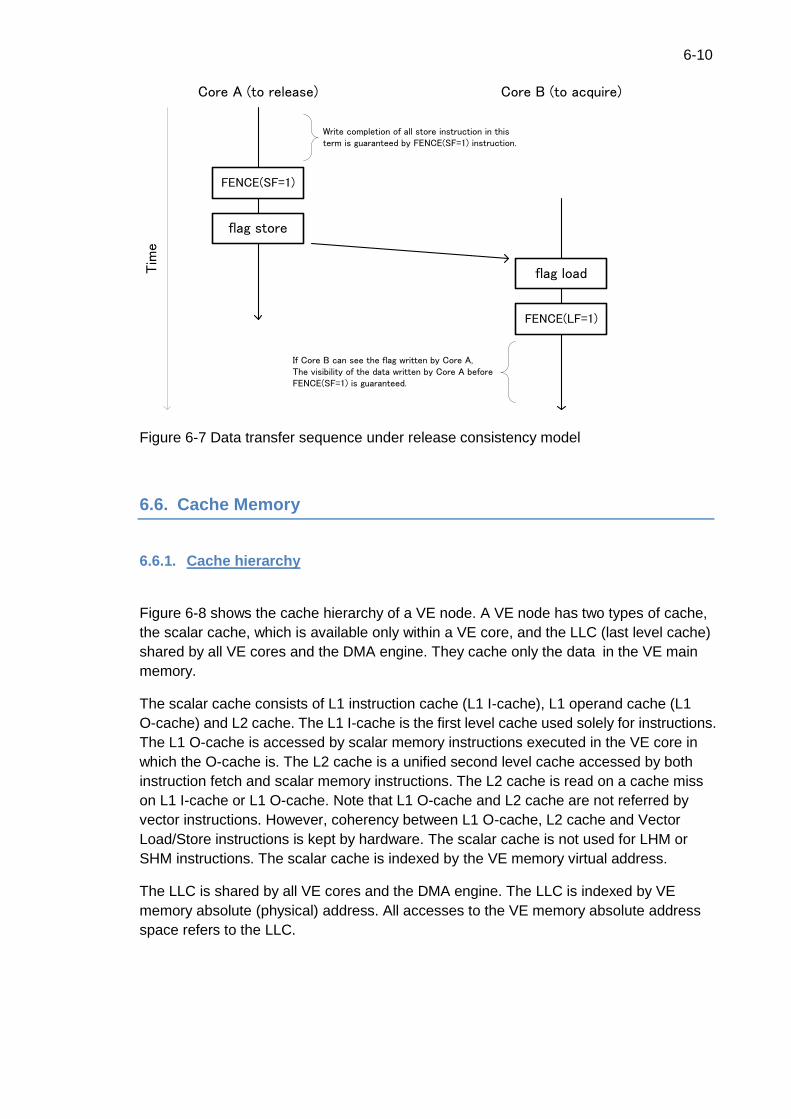
6-10
Figure 6-7 Data transfer sequence under release consistency model
6.6. Cache Memory
6.6.1. Cache hierarchy
Figure 6-8 shows the cache hierarchy of a VE node. A VE node has two types of cache,
the scalar cache, which is available only within a VE core, and the LLC (last level cache)
shared by all VE cores and the DMA engine. They cache only the data in the VE main
memory.
The scalar cache consists of L1 instruction cache (L1 I-cache), L1 operand cache (L1
O-cache) and L2 cache. The L1 I-cache is the first level cache used solely for instructions.
The L1 O-cache is accessed by scalar memory instructions executed in the VE core in
which the O-cache is. The L2 cache is a unified second level cache accessed by both
instruction fetch and scalar memory instructions. The L2 cache is read on a cache miss
on L1 I-cache or L1 O-cache. Note that L1 O-cache and L2 cache are not referred by
vector instructions. However, coherency between L1 O-cache, L2 cache and Vector
Load/Store instructions is kept by hardware. The scalar cache is not used for LHM or
SHM instructions. The scalar cache is indexed by the VE memory virtual address.
The LLC is shared by all VE cores and the DMA engine. The LLC is indexed by VE
memory absolute (physical) address. All accesses to the VE memory absolute address
space refers to the LLC.
FENCE(SF=1)
flag store
flag load
FENCE(LF=1)
Core A (to release) Core B (to acquire)
Write completion of all store instruction in this term is guaranteed by FENCE(SF=1) instruction.
If Core B can see the flag written by Core A, The visibility of the data written by Core A beforeFENCE(SF=1) is guaranteed.
Tim
e
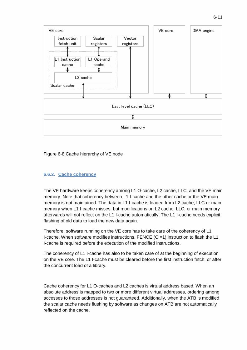
6-11
Figure 6-8 Cache hierarchy of VE node
6.6.2. Cache coherency
The VE hardware keeps coherency among L1 O-cache, L2 cache, LLC, and the VE main
memory. Note that coherency between L1 I-cache and the other cache or the VE main
memory is not maintained. The data in L1 I-cache is loaded from L2 cache, LLC or main
memory when L1 I-cache misses, but modifications on L2 cache, LLC, or main memory
afterwards will not reflect on the L1 I-cache automatically. The L1 I-cache needs explicit
flashing of old data to load the new data again.
Therefore, software running on the VE core has to take care of the coherency of L1
I-cache. When software modifies instructions, FENCE (CI=1) instruction to flash the L1
I-cache is required before the execution of the modified instructions.
The coherency of L1 I-cache has also to be taken care of at the beginning of execution
on the VE core. The L1 I-cache must be cleared before the first instruction fetch, or after
the concurrent load of a library.
Cache coherency for L1 O-caches and L2 caches is virtual address based. When an
absolute address is mapped to two or more different virtual addresses, ordering among
accesses to those addresses is not guaranteed. Additionally, when the ATB is modified
the scalar cache needs flushing by software as changes on ATB are not automatically
reflected on the cache.
L1 Instructioncache
L1 Operand cache
L2 cache
Scalar registers
Instructionfetch unit
Vector registers
VE core
Last level cache (LLC)
Main memory
Scalar cache
VE core DMA engine
6-12
6.6.3. Cache control
To keep the coherency of the scalar cache, SX-Aurora TSUBASA has a cache flush
feature, the FENCE instruction with commands CI, CD and C2 bit which correspond to L1
I-cache, L1 O-cache and L2 cache respectively. When the FENCE instruction with any of
CI, CD and/or C2 is ‘1’ is executed, all data in the corresponding cache is flushed and
following load instructions are halted until the flush completes.
6.6.4. Cache bypass
ATB has the ‘cache bypass’ attribute in each page descriptor. The scalar cache won’t
cache those pages with the cache bypass attribute ON. LLC will accommodate those
data, but may less-prioritize them in the replacement policy.
6.6.5. LLC
Data on the LLC can be categorized into two, temporal and sticky* data. The sticky data
is one which is more likely to stay in the cache to be used again in the near future. The
temporal data is what may not quite be used and therefore it is expected to be ousted
soon. The LLC gives a higher priority to sticky data and evicts temporal data more likely
than sticky ones. Note that mechanism does not guarantee the survival of the sticky data.
The LLC selects the data to be evicted taking various conditions such as the number of
accesses to the data, and the time it was lastly referred to, into consideration.
The priority class of the cached data is identified by type and VC bit of the instruction as
Table 5-.
*The word ‘sticky’ simply means it may have a higher priority to stay in the cache than the
other data that is not sticky, in terms of cache replacement policy. No guarantee about
the longevity of the data on the LLC.
Table 5-24 Priority class of cached data on LLC
Types and VC bit priority class
Instruction fetch Sticky
Scalar load Sticky
Scalar store Sticky
Vector load (VC=0) Temporal
Vector load (VC=1) Sticky
Vector store (VC=0) Temporal
Vector store (VC=1) Sticky

6-13
For the data accessed by the DMA engine or inbound accesses, the priority class is
decided by the hint in its DMA descriptor or the target hint table.
When the data as sticky is accessed by a temporal request, the data may turn temporal
and vice versa.
FENCE (CL=1) instruction forces all LLC-cached data to be temporal.
6-14
6.7. Communication Register
The CRs are shared by VE cores to provide for low latency communication among the
VE cores. A VE node has 1024 CRs. They can be used as the simple shared memory or
barrier synchronization counters as well.
6.7.1. Access to CR
CRs are addressed sequentially from 0 to 1023, and every 32 CRs compose a CR page.
Two ways to access CRs are provided, and both support atomic operations such as
test-and-set or fetch-and-increment.
CR access instructions
LCR, SCR, TSCR and FIDCR instructions provide a capability to access CRs. CR
directory (CRD) is used for address translation for CR access.
When LCR/SCR/TSCR or FIDCR is executed, CRD is referred to by bit 57-58 of its
effective address. If the valid bit of the referred entry is ‘1’,the target CR number is
generated with the CR page number from the CRD entry and bit 59-63 of the effective
address as its offset. When the entry is invalid a memory access exception is raised.
6-15
Figure 6-25 Address translation on CR access by CR access instruction
CR directory (CRD)
Four entries of CR directory (CRD) are provided for CR address translation from a logical
CR to a physical CR. Each CRD entry consists a 64 bit register including a valid bit and a
5 bit pointer to the CR page#.
~~
32W
32W
32W
32W
32W
32W
~~
0 63
Communication
Registers
0
32
64
96
128
160
992
1023
57 59 63
CR Directory
V 0 4
Effective address
0 1 58 59 63
V CR page#
6-16
Access through VE CR absolute address space
The CRs are mapped on the VE CR absolute address space. VE cores, the DMA engine,
VH and external PCIe devices can access CRs through the mapped region. The mapping
is redundant in that the address includes a function in itself. In other words, address for a
physical CR may change depending on the function that is being applied on the CR, such
as simple read/write or atomic operations. Figure 6-9 shows the addressing for CRs.
46 63
CR page
50
CR #funcMust be
zero
55 600
SYN
C
51
Figure 6-9 Addressing of the VE CR absolute address
CR page, bit 46-50CR page number.
CR number, bit 56-60
CR offset address within the CR page.
Func, bit 52-55
Function applied in this access. For details, see Table 5-1.
SYNC, bit51
Not used.
Table 5.2 shows the functions for CR access through the VE CR absolute address space.
Note that read requests may have side effects on the contents of CRs.
VE CR absolute address space must be accessed in an 8 byte size, with an alignment to
an 8-byte boundary. Otherwise, memory access exception will occur.
Any access with an undefined function causes memory access exception.
CR cache in a VE core is not updated by the LHM/SHM or DMA access through VE CR
absolute address space, or inbound accesses. When a VE core and the VH or external
PCIe devices operate the same CR at the same time, VE core should observe the CR by
LCR or FIDCR (Rz=7) instruction to bypass its CR cache.
Table 5-1 Function of CR access through VE CR absolute address space
Func ¥Type
Remarks Read Write
0000 return CR(x) CR(x) D Corresponds to LCR/SCR.
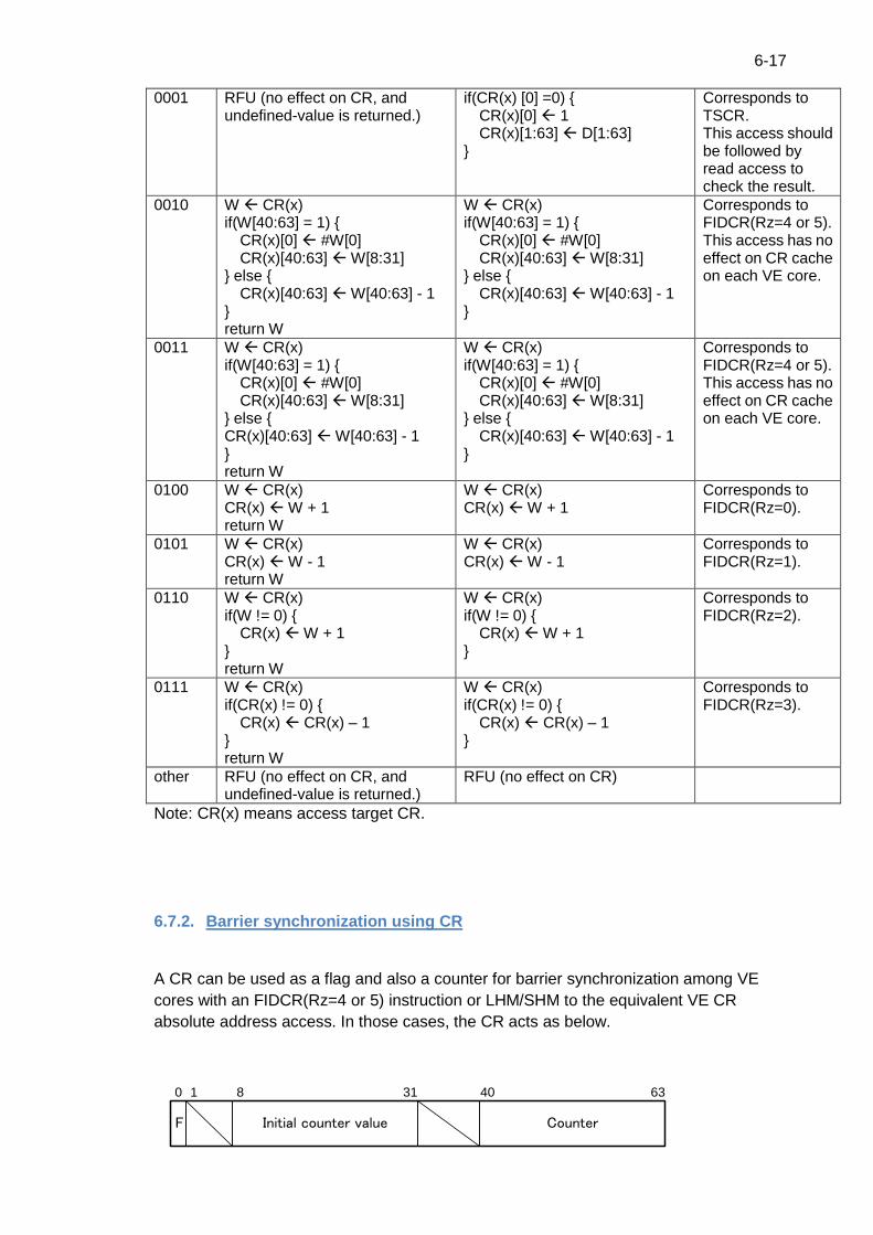
6-17
0001 RFU (no effect on CR, and undefined-value is returned.)
if(CR(x) [0] =0) { CR(x)[0] 1 CR(x)[1:63] D[1:63]
}
Corresponds to TSCR. This access should be followed by read access to check the result.
0010 W CR(x) if(W[40:63] = 1) {
CR(x)[0] #W[0] CR(x)[40:63] W[8:31]
} else { CR(x)[40:63] W[40:63] - 1
} return W
W CR(x) if(W[40:63] = 1) {
CR(x)[0] #W[0] CR(x)[40:63] W[8:31]
} else { CR(x)[40:63] W[40:63] - 1
}
Corresponds to FIDCR(Rz=4 or 5). This access has no effect on CR cache on each VE core.
0011 W CR(x) if(W[40:63] = 1) {
CR(x)[0] #W[0] CR(x)[40:63] W[8:31]
} else { CR(x)[40:63] W[40:63] - 1 } return W
W CR(x) if(W[40:63] = 1) {
CR(x)[0] #W[0] CR(x)[40:63] W[8:31]
} else { CR(x)[40:63] W[40:63] - 1
}
Corresponds to FIDCR(Rz=4 or 5). This access has no effect on CR cache on each VE core.
0100 W CR(x) CR(x) W + 1 return W
W CR(x) CR(x) W + 1
Corresponds to FIDCR(Rz=0).
0101 W CR(x) CR(x) W - 1 return W
W CR(x) CR(x) W - 1
Corresponds to FIDCR(Rz=1).
0110 W CR(x) if(W != 0) {
CR(x) W + 1 } return W
W CR(x) if(W != 0) {
CR(x) W + 1 }
Corresponds to FIDCR(Rz=2).
0111 W CR(x) if(CR(x) != 0) {
CR(x) CR(x) – 1 } return W
W CR(x) if(CR(x) != 0) {
CR(x) CR(x) – 1 }
Corresponds to FIDCR(Rz=3).
other RFU (no effect on CR, and undefined-value is returned.)
RFU (no effect on CR)
Note: CR(x) means access target CR.
6.7.2. Barrier synchronization using CR
A CR can be used as a flag and also a counter for barrier synchronization among VE
cores with an FIDCR(Rz=4 or 5) instruction or LHM/SHM to the equivalent VE CR
absolute address access. In those cases, the CR acts as below.
31 63
Initial counter value
40
CounterF
0 1 8
6-18
Figure 6-10 Interpretation of bits of CR for barrier synchronization
Flag, bit 0
This is the flag to indicate current phase of the synchronization. This flag is inverted when
the next synchronization is met.
Counter, bit 40-63
This is a 24bit counter for barrier synchronization. This counter may indicate the number
of participants which have not reached the synchronization condition.
Initial counter value, bit 8-31
This is a 24bit field to hold the initial value for the counter. This number is only referred at
the end of synchronization as the initial value of the counter bit40-63.
At first, initial values are set for the flag, the counter, and the initial counter value.
Typically the flag is initialized to ‘0’ and both the counter and the initial counter value are
set to the number of participants of the synchronization. The counter is decremented by
FIDCR (Rz=4 or 5) instruction or equivalent VE CR absolute address access. When the
counter value reaches zero, the synchronization is finished and the counter rewinds to
the initial value. The flag is inverted to indicate that the synchronization has completed.
The participants of the synchronization can detect the finish of the synchronization by
reading the inverted flag.
CR Cache
CR cache helps efficient barrier synchronization using CRs. CR cache can hold a copy of
bit 0, the synchronization flag, of CRs, and provides low latency access to the CR copy
for some specific use. To utilize CR cache, VE cores need to use FIDCR (Rz=4 or 6)
instruction. To the other instructions, CR cache may not be valid.
CR cache has following functions.
1. Registration
When a VE core executes FIDCR (Rz=4 or 6) instruction and CR cache does not hold the
copy of the destination CR, the value of the bit 0 of the destination CR is stored in the CR
cache. In the case of FIDCR (Rz=4), the value after the update is stored.
2. Update
When a VE core executes FIDCR (Rz=4) instruction and CR cache have the copy of the
destination CR, the cached data is updated with the result of FIDCR (Rz=4).
6-19
Also, CR update message is broadcasted to every VE cores when bit 0 of a CR is
updated by FIDCR (Rz=4 or 5) executed in any of VE cores. Upon arrival of the massage,
the CR cache updates its copy if it holds the copy of the updated CR.
3. Reference
When a VE core executes FIDCR (Rz=6) instruction, the data is returned from the CR
cache if the CR cache has the copy of the destination CR. Otherwise, the data is read
from the destination CR. Note that CR cache hold copy of bit 0 only. For the former case,
r the bit1-63 of the returned value is undefined.
4. Invalidation
When a VE core executes SCR, TSCR, or FIDCR (Rz=0,1,2, 3, 5 or 7) instruction, the
cached data for the target CR is invalidated from the CR cache. The cached data is also
invalidated when the entry of CR directory corresponding to the data is updated.
Note that the size and configuration of CR cache and its replacement policy is system
dependent. Also, CR cache may discard cached data anytime. The permanence of
cached data is not guaranteed.
Example of a barrier synchronization
The following is a sample scenario for barrier synchronization using the CR cache. This
example assumes core A, B and C as the participants of the synchronization, and CR[0]
is used as the barrier synchronization counter.
1. Core A initializes CR[0]. The flag (bit 0) is set to ‘0’, and the counter (bit 40-63)
and initial counter value (bit 8-31) are set to ‘3’.
2. Core A, B and C start computation in parallel.
3. Let’s say core A reaches the barrier point first. Then core A executes FIDCR
(Rz=4) instruction, and the value in CR[0] is stored into the target scalar register
and the counter field of the CR[0] is decremented to ‘2’. Then the result value of
CR[0]’s bit0 , which is still zero, is stored into the CR cache of core A.
4. Core A starts polling looking in CR[0] until the synchronization condition is met..
The polling includes FIDCR (Rz=6) and the reply of the FIDCR (Rz=6) comes
from the CR cache. Core A checks if the result value FIDCR has been flipped to
one, in other words, the participant cores have all reached each barrier point. If
yes, Core A escapes the polling loop.
5. Core B reaches the barrier point and executes FIDCR (Rz=4) instruction. The
counter field of CR[0] is decremented to ‘1’. The flag field is still unchanged.
Core B also starts to poll CR[0] as core A does.
6. Finally core C reaches the barrier point and execute FIDCR (Rz=4) instruction.
The counter field of CR[0] is decremented to ‘0’. Now the synchronization
condition is satisfied.. The flag field of CR[0] is inverted to ‘1’, and counter is set
back to ‘3’.Then an update message is broadcasted to all cores (Note: the

6-20
broadcast message arrives to not just the participant cores, but all available
cores in the VE.) CR caches in the cores are all updated to the new value ‘1’ by
the message. By the way the FIDCR (Rz=4) of Core C returns the value before
the synchronization is made, therefore the last comer core C still needs to get
into the polling loop anyway, and it escapes the loop soon.
7. Now Core A, B and C are all synchronized, and they step forward again.
7. Exceptions
7.1. Exceptions and interrupts
A VE core raises an interrupt when the VE core encounters a problem hindering the
program from continuing processing any more, or the VE core reached a condition where
it raises interrupt(s) to the host due to MONC instruction or some debug feature. The
former causes are typically called exceptions and the latter are called interrupts or traps.
In this section, we collectively call them interrupts.
Table 7-1 shows the cause of interrupts. When a VE core detects interrupt cause(s), the
VE core raises an interrupt by asserting the corresponding bit(s) of the interrupt cause
field in EXS and starts the halt execution sequence.
Table 7-1 : Causes of interrupt
bit Name major cause
0 Memory protection exception Store to a write-inhibited page.
1 Missing page exception Page not found
2 Missing space exception Space not found
3 Memory access exception Other Invalid Memory access detected
4-7 (Reserved) -
8 Division exception Zero division detected.
9 Floating-point overflow exception Overflow in floating point calculation
10 Floating-point underflow exception Underflow in floating point calculation
11 Fixed-point overflow exception Overflow in fixed point calculation
12 Invalid operation exception Invalid operation in floating point
calculation
13 Inexact exception Inexact result in floating point
calculation
14-16 (Reserved) -
17 Illegal instruction format exception An undefined instruction executed
7-1
18 Illegal data format exception VL > MVL etc.
19 Software interrupt (MONC) Execution of MONC instruction.
20 Address match interrupt Store to the pre-set address is detected.
Prepared for debugger use
21 Branch trap
Execution of branch instructions (BC,
BCS, BCF, BSIC, BCR) in the branch
trap mode.
22 One step interrupt An instruction was executed in the
one-step interrupt mode.
23 Software interrupt (MONC TRAP)
Execution of MONC (Cx=1) instruction.
Note: when this turns one bit19 is also
one.
24 Host memory protection exception Store to a write-inhibited page.
25 Host missing page exception Page on host memory not found
26 Host missing space exception Space on host memory not found
27 Host memory access exception Host memory access to unavailable
address detected
28 I/O access exception Timeout in LHM execution
29-39 (Reserved) -
7.1.1. Attributes of interrupts
SX-Aurora TSUBASA has two types of interrupts, recoverable and unrecoverable ones.
VE cores can restart their execution of program from a recoverable interrupt followed by
appropriate interrupt handling by the VH. Restarting from an unrecoverable interrupt is
not supported.
Recoverable exceptions are:
・ Software interrupt (MONC)
・ Software interrupt (MONC TRAP)
・ Address matched interrupt
・ One-step interrupt
・ Branch trap
7-2
Interrupts caused by certain kinds of exceptions are maskable. Each maskable exception
has a corresponding mask bit and an exception flag in PSW. When the mask bit is set to
“0”, the interrupt due to the corresponding exception is not raised. Note that the exception
itself is recorded in the exception flag regardless of the mask bit.
Maskable exceptions are:
・ Division exception (DIV)
・ Floating-point overflow exception (FOF)
・ Floating-point underflow exception (FUF)
・ Fixed-point overflow exception (XOF)・ Invalid operation exception (INV)
・ Inexact exception (INE)
7.1.2. Causes of interrupts
Memory protection exception
Cause(s):
Memory instruction attempted to store data to a write prohibited page.
LHM and SHM are out of this interrupt’s scope.
Missing page exception
Cause(s):
1) Instruction fetch from an unavailable page (Bit 63 of page descriptor is ‘1’)
2) Execution of an instruction which attempts to access an unavailable page.
LHM and SHM are out of this interrupt’s scope.
Missing space exception
Cause(s):
1) Instruction fetch to the address that is not available in partial space directory.
2) Execution of an instruction with memory access to the address that is not
available in partial space directory.
LHM and SHM are out of this interrupt’s scope.
7-3
Memory access exception
Cause(s):
1) Access to unavailable VE memory absolute address
・ Instruction fetch from an unavailable VE memory absolute address, such as
accessing the memory beyond its physical memory size.
・ Reading/Writing from/to an unavailable VE memory absolute address.
2) Memory boundary violation
・ Atomic memory access instructions violating their 4 or 8 byte memory
boundary rule
・ Vector memory access instructions violating their 4 or 8 byte memory
boundary rule
・ Branch instructions which are ‘taken’ and attempting to branch to a
non-8byte-aligned address
・ Host memory access instructions violating their memory boundary rule
depending on their access size
3) CR access violation
・ CR access instructions attempting to access an unavailable CR page
・ CR access instructions attempting to access a not-existing CR
4) Access over multiple spaces of different page sizes
・ A vector memory instruction attempting to access over two or more partial
spaces of different page size
5) Partial space multiple-hit
・ Instruction fetch from the address that resides in multiple partial spaces.
Illegal space reservation on ATB.
・ Execution of an instruction that attempts to access the address that resides
in multiple partial spaces. Illegal space reservation on ATB.
LHM and SHM are out of this interrupt’s scope.
Host memory protection exception
Cause(s):
Execution of a SHM instruction which attempts to store data to a write prohibit page.
7-4
Host missing page exception
Cause(s):
Execution of a LHM or SHM instruction which attempts to access an unavailable page
Host missing space exception
Cause(s):
The partial space corresponding to the target address of LHM/SHM is not available.
Host memory access exception
Cause(s):
1) Access to unavailable absolute address
・ LHM or SHM instruction targeting to an unavailable VE memory absolute
address
・ LHM or SHM instruction targeting to an unavailable VE register absolute
address
・ LHM or SHM instruction targeting to an unavailable VE communication
register absolute address
2) Memory boundary violation
・ LHM or SHM instruction which violates the 2, 4 or 8 byte boundary rule.
・ 1, 2 or 4 byte SHM targeting to a VE register absolute address
・ 1, 2 or 4 byte LHM/SHM targeting to a VE communication register absolute
address
3) CR access violation
・ LHM or SHM instruction targeting to a not-existing number of CR
・ LHM or SHM instruction targeting to a CR with an undefined function.
4) Partial space multi-hit

7-5
・ LHM or SHM instruction accesses an address which hits multiple partial
spaces
5) Access to undefined address space
・ LHM or SHM instruction accesses an undefined type of address space
I/O Access Exceptions
Cause(s):
An LHM or SHM instruction timed-out
Division exception
Cause(s):
Divide by zero detected
Floating-point overflow exception
Cause(s):
Floating-point overflow on floating-point arithmetic instructions
Floating-point underflow exception
Cause(s):
Floating-point underflow on floating-point arithmetic instructions
Fixed-point overflow exception
Cause(s):
Overflow on fixed-point arithmetic instructions or shift operation instructions.
7-6
Invalid operation exception
Cause(s):
Invalid operation on floating-point arithmetic instructions
Inexact exception
Cause(s):
Inexact result on floating-point arithmetic instructions
Illegal instruction format exception
Cause(s):
Following illegal formed instructions are fetched and decoded.
1) An instruction with an undefined opcode
2) A RW type instruction with invalid register number
3) A RV type instruction with invalid control flags.
4) A RV type instruction with invalid mask field.
Illegal data format exception
Cause(s):
1) Execution of a LVL instruction which attempts to set a number exceeding MVL
into VL.
2) Execution of a vector instruction with VL exceeding MVL.
Software interrupt (MONC)
Cause(s):
7-7
A MONC instruction is executed.
Result(s):
IC: The address of the instruction next to the MONC instruction
Software interrupt (MONC TRAP)
Cause(s):
Execution of a MONC (Cx=1) instruction
Result(s):
IC: The address of the instruction next to the MONC instruction
Address match interrupt
This capability is mainly used by debuggers.
Cause(s):
Execution of a store instruction which attempts to store data to the address where
specified by store address register.
Branch trap
This capability is mainly used by debuggers.
Cause(s):
Execution of branch instruction under the branch trap mode, where branch instructions
are BC, BCS, BCF, BSIC and BCR.
One step interrupt
This capability is mainly used by debuggers, especially for stepping run.
Cause(s):
Execution of any instruction under one the step interrupt mode.
Result(s):
IC: The address for the restart point, which is branch target address if the last
executed instruction is a taken branch instruction, or the address next to the last
executed instruction otherwise.

7-8
7.1.3. Fast synchronization debug interrupt flag
SX-Aurora TSUBASA supports ‘Fast synchronization debug interrupt’ for debugging of
parallel programs over multiple cores.
8. Instructions
8.1. Legends
This chapter describes the formats and the functions of the instructions executed by the
central processing unit (CPU) of this system.
8.1.1. Desctiption of the function
・Name of the instruction
・Format Although cross-out fields in instruction formats are ignored by the
CPU, they should be 0(SBZ) for future extensions.
・Function The function of the instruction is shown.
・Exceptions Exceptions possibly caused by the instruction are listed.
8.1.2. Operators
+ : Addition
- : Subtraction
* : Multiplication
/ : Division
% : Modulo operation
& : Logical AND (AND)
| : Logical OR (OR)
+ : Exclusive logical OR (XOR)
≡ : Equivalence (exclusive NOR)
~ : Negation (Bit inversion)
B << A : Left shift B by A
B >> A : Right shift B by A
C ? A : B : When C=1 this operation returns A, otherwise B is returned.
8-1
Σ(A, B, …) : Summation (the total sum of A, B, …)
8.1.3. Keywords and notations
M(A, B) : B-byte memory contents or location at the effective address given by the
contents of A. When B is omitted it is regarded as 1.
EA Operation address, calculated by each fields of an instruction.
A[i] bit i of A
A[i:j] from bit i to bit j of A
(A, B) Concatenated value of A on the left of B
A B Storing (moving) of the contents of B into A.
Sx Immediate value or S register designated by x field of instruction word.
Sy Immediate value or S register designated by y field of instruction word.
Sz Immediate value or S register designated by z field of instruction word.
Sw Immediate value or S register designated by w field of instruction word.
Vx V register designated by Vx field of instruction word.
Vy V register designated by Vy field of instruction word.
Vz V register designated by Vz field of instruction word.
Vw V register designated by Vw field of instruction word.
Vx(i) i-th element of Vx.
Vy(i) i-th element of Vy.
Vz(i) i-th element of Vz.
Vw(i) i-th element of Vw.
VMx VM register designated Vx field of instruction word.
VMy VM register designated Vy field of instruction word.
VMz VM register designated Vz field of instruction word.
VM VM register designated M field of instruction word.
mod(A, B) The remainder of A divided by B. Unless specified, A is treated as
an unsigned interger.
sext(A, B) B-bit value is generated by extending the sign bit
8-2
(Most significant bit) of A.
cond(A, B, C) The result of comparison B and C in A condition.
C can be omitted and in this case C is handled as 0.
Refer to Chapter 5 for system interpretation of comparison
condition
max(A, B) Maximum value of A and B.
min(A, B) Minimum value of A and B.
8.1.4. Syntax
If-else syntax:
Notation: if (A) {B} else if (C) {D} else {E}
Operation: If A is true, B is executed.
If A is not true and C is true, D is executed.
If both of A and C are not true, E is executed.
for syntax: Iterative operation
Notation: for (i = A to B) {C}
Operation: C is executed for each i from A to B. When A>B
C is not executed.
8-3
8.1.5. Endianness
The Aurora VE CPU stores/loads data to/from the memory in the little endian byte
order. When storing/loading more than 2 bytes data into/from the memory,
hardware takes care of its endianness properly.
8.1.6. Vector elements
The element number of V registers is not written unless otherwise specified, and
from element #0 to #VL-1 are operated together in a vector operation by default.
Formaskable vector instructions, only elements corresponding to the bit pattern in
the VM designated the M field are valid as their input operands or destinations.
Unless otherwise mentioned, vector elements that are not the objects of vector
operations preserve their contents.
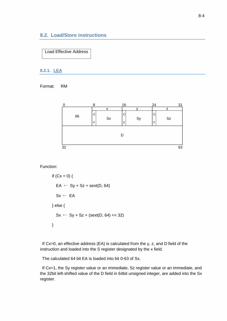
8-4
8.2. Load/Store instructions
Load Effective Address
8.2.1. LEA
Format: RM
x
06 Sx Sy Sz
y
C
y
z
C
z
8 16 24 31
D
32 63
0
C
x
Function:
if (Cx = 0) {
EA ← Sy + Sz + sext(D, 64)
Sx ← EA
} else {
Sx ← Sy + Sz + (sext(D, 64) << 32)
}
If Cx=0, an effective address (EA) is calculated from the y, z, and D field of the
instruction and loaded into the S register designated by the x field.
The calculated 64 bit EA is loaded into bit 0-63 of Sx.
If Cx=1, the Sy register value or an immediate, Sz register value or an immediate, and
the 32bit left-shifted value of the D field in 64bit unsigned integer, are added into the Sx
register.

8-5
Exception: None
Notes:
・When Cz=0 the z operand is regarded as 0 regardless of Sz.
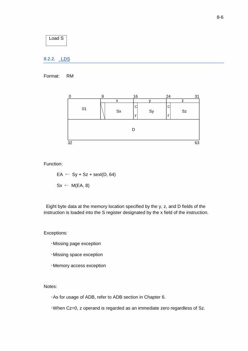
8-6
Load S
8.2.2. LDS
Format: RM
x
01 Sx Sy Sz
y
C
y
z
C
z
8 16 24 31
D
32 63
0
Function:
EA ← Sy + Sz + sext(D, 64)
Sx ← M(EA, 8)
Eight byte data at the memory location specified by the y, z, and D fields of the
instruction is loaded into the S register designated by the x field of the instruction.
Exceptions:
・Missing page exception
・Missing space exception
・Memory access exception
Notes:
・As for usage of ADB, refer to ADB section in Chapter 6.
・When Cz=0, z operand is regarded as an immediate zero regardless of Sz.
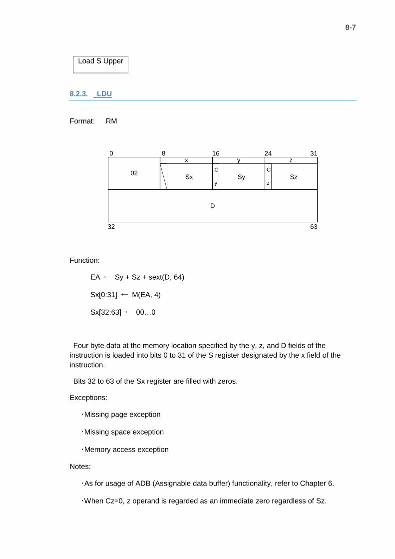
8-7
Load S Upper
8.2.3. LDU
Format: RM
x
02 Sx Sy Sz
y
C
y
z
C
z
8 16 24 31
D
32 63
0
Function:
EA ← Sy + Sz + sext(D, 64)
Sx[0:31] ← M(EA, 4)
Sx[32:63] ← 00…0
Four byte data at the memory location specified by the y, z, and D fields of the
instruction is loaded into bits 0 to 31 of the S register designated by the x field of the
instruction.
Bits 32 to 63 of the Sx register are filled with zeros.
Exceptions:
・Missing page exception
・Missing space exception
・Memory access exception
Notes:
・As for usage of ADB (Assignable data buffer) functionality, refer to Chapter 6.
・When Cz=0, z operand is regarded as an immediate zero regardless of Sz.
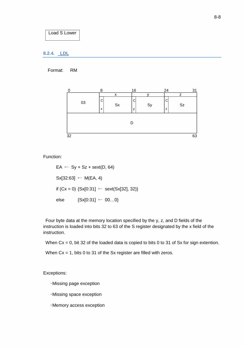
8-8
Load S Lower
8.2.4. LDL
Format: RM
x
03 Sx Sy Sz
y
C
y
z
C
z
8 16 24 31
D
32 63
0
C
x
Function:
EA ← Sy + Sz + sext(D, 64)
Sx[32:63] ← M(EA, 4)
if (Cx = 0) {Sx[0:31] ← sext(Sx[32], 32)}
else {Sx[0:31] ← 00…0}
Four byte data at the memory location specified by the y, z, and D fields of the
instruction is loaded into bits 32 to 63 of the S register designated by the x field of the
instruction.
When Cx = 0, bit 32 of the loaded data is copied to bits 0 to 31 of Sx for sign extention.
When Cx = 1, bits 0 to 31 of the Sx register are filled with zeros.
Exceptions:
・Missing page exception
・Missing space exception
・Memory access exception

8-9
Notes:
・As for usage of ADB functionality, refer to Chapter 6.
・When Cz=0, z operand is regarded as an immediate zero regardless of Sz.
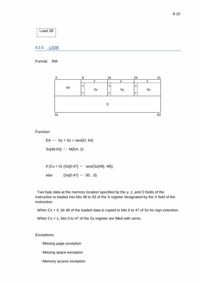
8-10
Load 2B
8.2.5. LD2B
Format: RM
x
04 Sx Sy Sz
y
C
y
z
C
z
8 16 24 31
D
32 63
0
C
x
Function:
EA ← Sy + Sz + sext(D, 64)
Sx[48:63] ← M(EA, 2)
if (Cx = 0) {Sx[0:47] ← sext(Sx[48], 48)}
else {Sx[0:47] ← 00…0}
Two byte data at the memory location specified by the y, z, and D fields of the
instruction is loaded into bits 48 to 63 of the S register designated by the X field of the
instruction.
When Cx = 0, bit 48 of the loaded data is copied to bits 0 to 47 of Sx for sign extention.
When Cx = 1, bits 0 to 47 of the Sx register are filled with zeros.
Exceptions:
・Missing page exception
・Missing space exception
・Memory access exception

8-11
Notes:
・As for usage of ADB functionality, refer to Chapter 6.
・When Cz=0, z operand is regarded as an immediate zero regardless of Sz.
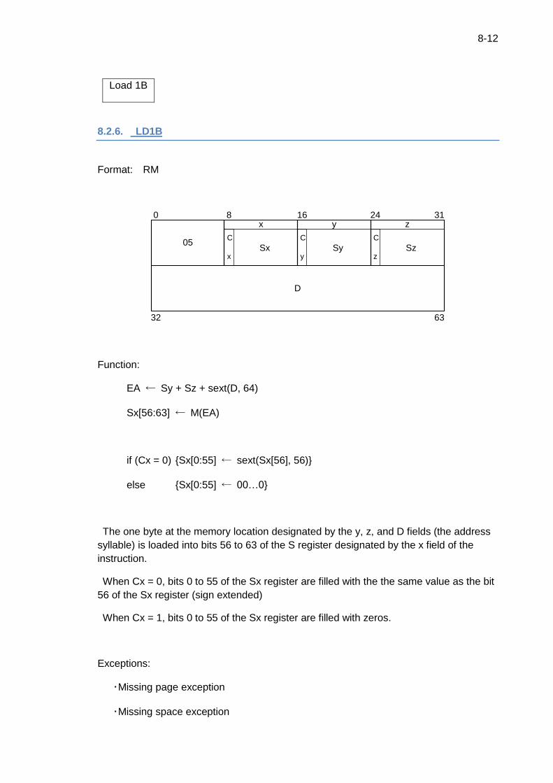
8-12
Load 1B
8.2.6. LD1B
Format: RM
x
05 Sx Sy Sz
y
C
y
z
C
z
8 16 24 31
D
32 63
0
C
x
Function:
EA ← Sy + Sz + sext(D, 64)
Sx[56:63] ← M(EA)
if (Cx = 0) {Sx[0:55] ← sext(Sx[56], 56)}
else {Sx[0:55] ← 00…0}
The one byte at the memory location designated by the y, z, and D fields (the address
syllable) is loaded into bits 56 to 63 of the S register designated by the x field of the
instruction.
When Cx = 0, bits 0 to 55 of the Sx register are filled with the the same value as the bit
56 of the Sx register (sign extended)
When Cx = 1, bits 0 to 55 of the Sx register are filled with zeros.
Exceptions:
・Missing page exception
・Missing space exception
8-13
・Memory access exception
Notes:
・As for usage of ADB functionality, refer to Chapter 6.
・When Cz=0, z operand is regarded as an immediate zero regardless of Sz.
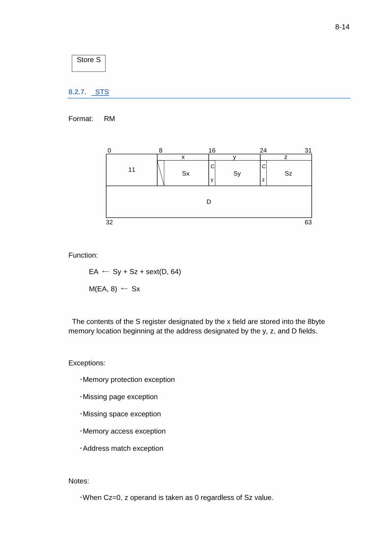
8-14
Store S
8.2.7. STS
Format: RM
x
11 Sx Sy Sz
y
C
y
z
C
z
8 16 24 31
D
32 63
0
Function:
EA ← Sy + Sz + sext(D, 64)
M(EA, 8) ← Sx
The contents of the S register designated by the x field are stored into the 8byte
memory location beginning at the address designated by the y, z, and D fields.
Exceptions:
・Memory protection exception
・Missing page exception
・Missing space exception
・Memory access exception
・Address match exception
Notes:
・When Cz=0, z operand is taken as 0 regardless of Sz value.
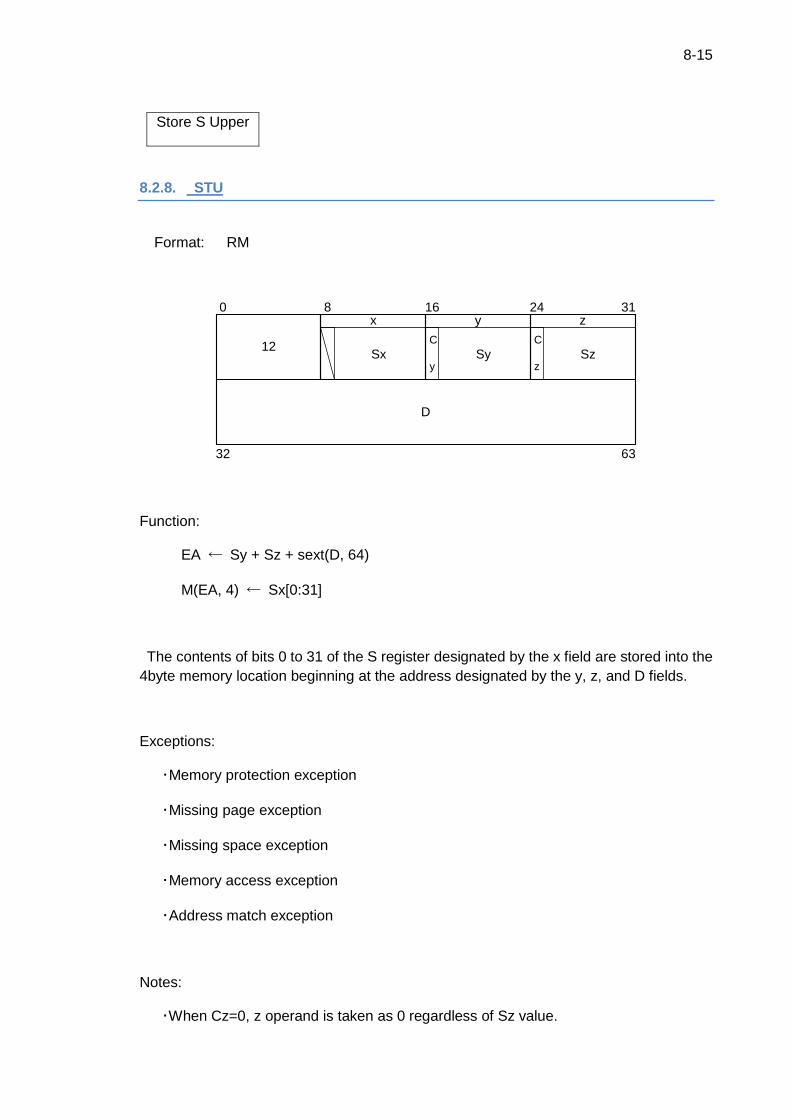
8-15
Store S Upper
8.2.8. STU
Format: RM
x
12 Sx Sy Sz
y
C
y
z
C
z
8 16 24 31
D
32 63
0
Function:
EA ← Sy + Sz + sext(D, 64)
M(EA, 4) ← Sx[0:31]
The contents of bits 0 to 31 of the S register designated by the x field are stored into the
4byte memory location beginning at the address designated by the y, z, and D fields.
Exceptions:
・Memory protection exception
・Missing page exception
・Missing space exception
・Memory access exception
・Address match exception
Notes:
・When Cz=0, z operand is taken as 0 regardless of Sz value.

8-16
Store S Lower
8.2.9. STL
Format: RM
x
13 Sx Sy Sz
y
C
y
z
C
z
8 16 24 31
D
32 63
0
Function:
EA ← Sy + Sz + sext(D, 64)
M(EA, 4) ← Sx[32:63]
The contents of bits 32 to 63 of the S register designated by the x field are stored into
the 4byte memory location beginning at the address designated by the y, z, and D fields.
Exceptions:
・Memory protection exception
・Missing page exception
・Missing space exception
・Memory access exception
・Address match exception
Notes:
・When Cz=0, z operand is taken as 0 regardless of Sz value.
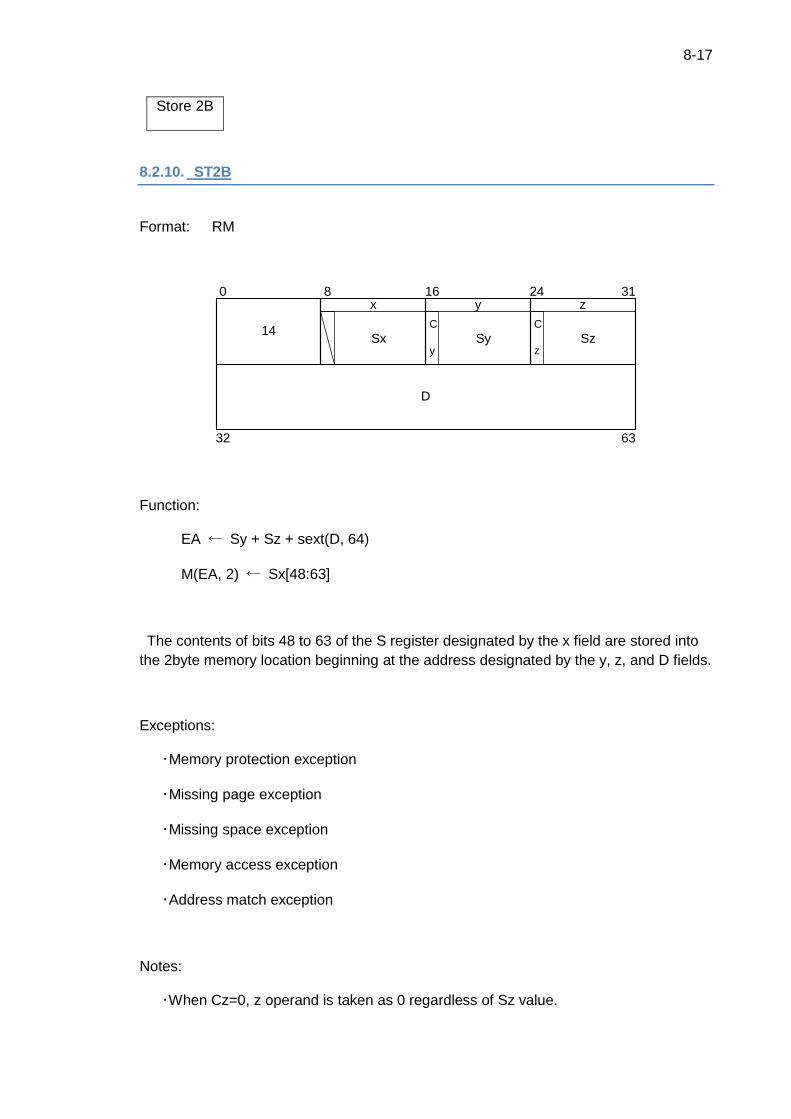
8-17
Store 2B
8.2.10. ST2B
Format: RM
x
14 Sx Sy Sz
y
C
y
z
C
z
8 16 24 31
D
32 63
0
Function:
EA ← Sy + Sz + sext(D, 64)
M(EA, 2) ← Sx[48:63]
The contents of bits 48 to 63 of the S register designated by the x field are stored into
the 2byte memory location beginning at the address designated by the y, z, and D fields.
Exceptions:
・Memory protection exception
・Missing page exception
・Missing space exception
・Memory access exception
・Address match exception
Notes:
・When Cz=0, z operand is taken as 0 regardless of Sz value.
8-18
Store 1B
8.2.11. ST1B
Format: RM
x
15 Sx Sy Sz
y
C
y
z
C
z
8 16 24 31
D
32 63
0
Function:
EA ← Sy + Sz + sext(D, 64)
M(EA) ← Sx[56:63]
The contents of bits 56 to 63 of the S register designated by the x field are stored into
the 1byte memory location beginning at the address designated by the y, z, and D fields.
Exceptions:
・Memory protection exception
・Missing page exception
・Missing space exception
・Memory access exception
・Address match exception
Notes:
・When Cz=0, z operand is taken as 0 regardless of Sz value.
8-19
Dismissable Load S
8.2.12. DLDS
Format: RM
x
09 Sx Sy Sz
y
C
y
z
C
z
8 16 24 31
D
32 63
0
Function:
EA ← Sy + Sz + sext(D, 64)
Sx ← M(EA, 8)
The 8-byte data beginning at the memory byte location designated by the (y, z and D)
field is loaded into the S register designated by the x field of the instruction.
No exception is detected regarding this instruction.
When a nonexistent or inaccessible memory area is specified, an unexpected value
may be loaded.
Exceptions: None
Notes:
・As for usage of ADB, refer to ADB section in Chapter 6.
・When Cz=0, z operand is taken as 0 regardless of Sz value.
8-20
Dismissable Load Upper
8.2.13. DLDU
Format: RM
x
0A Sx Sy Sz
y
C
y
z
C
z
8 16 24 31
D
32 63
0
Function:
EA ← Sy + Sz + sext(D, 64)
Sx[0:31] ← M(EA, 4)
Sx[32:63] ← 00…0
The 4-byte data beginning at the memory byte location designated by the (y, z and D)
field is loaded into bits 0 to 31 of the S register designated by the x field of the instruction.
Bit 32 to 63 of the S register designated by the x field are filled with zeros.
No exception is detected regarding this instruction.
When a nonexistent or inaccessible memory area is specified, an unexpected value
may be loaded.
Exceptions: None
Notes:
・As for usage of ADB, refer to ADB section in Chapter 6.
・When Cz=0, z operand is taken as 0 regardless of Sz value.
8-21
Dismissable Load Lower
8.2.14. DLDL
Format: RM
C
x
x
0B Sx Sy Sz
y
C
y
z
C
z
8 16 24 31
D
32 63
0
Function:
EA ← Sy + Sz + sext(D, 64)
Sx[32:63] ← M(EA, 4)
if (Cx = 0) {Sx[0:31] ← sext(Sx[32], 32)}
else {Sx[0:31] ← 00…0}
The 4-byte data beginning at the memory byte location designated by the (y, z and D)
field is loaded into bits 32 to 63 of the S register designated by the x field of the
instruction.
When Cx = 0, bit 0 to 31 of the Sx register are filled with the the same value as the bit 32
of the Sx register (sign extended)
When Cx = 1, bit 0 to 31 of the Sx register are filled with zeros.
No exception is detected regarding this instruction.
When a nonexistent or inaccessible memory area is specified, an unexpected value
may be loaded.
Exceptions: None

8-22
Notes:
・As for usage of ADB, refer to ADB section in Chapter 6.
・When Cz=0, z operand is taken as 0 regardless of Sz value.
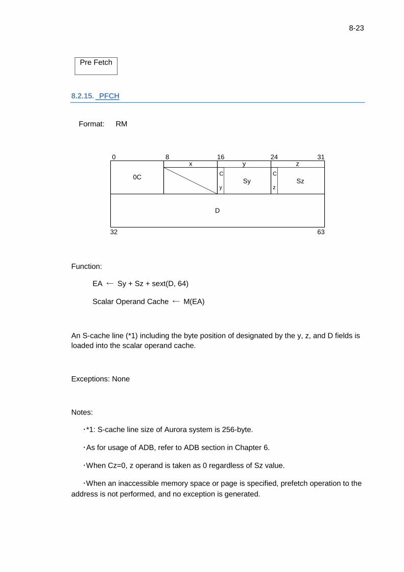
8-23
Pre Fetch
8.2.15. PFCH
Format: RM
x
0C Sy Sz
y
C
y
z
C
z
8 16 24 31
D
32 63
0
Function:
EA ← Sy + Sz + sext(D, 64)
Scalar Operand Cache ← M(EA)
An S-cache line (*1) including the byte position of designated by the y, z, and D fields is
loaded into the scalar operand cache.
Exceptions: None
Notes:
・*1: S-cache line size of Aurora system is 256-byte.
・As for usage of ADB, refer to ADB section in Chapter 6.
・When Cz=0, z operand is taken as 0 regardless of Sz value.
・When an inaccessible memory space or page is specified, prefetch operation to the
address is not performed, and no exception is generated.
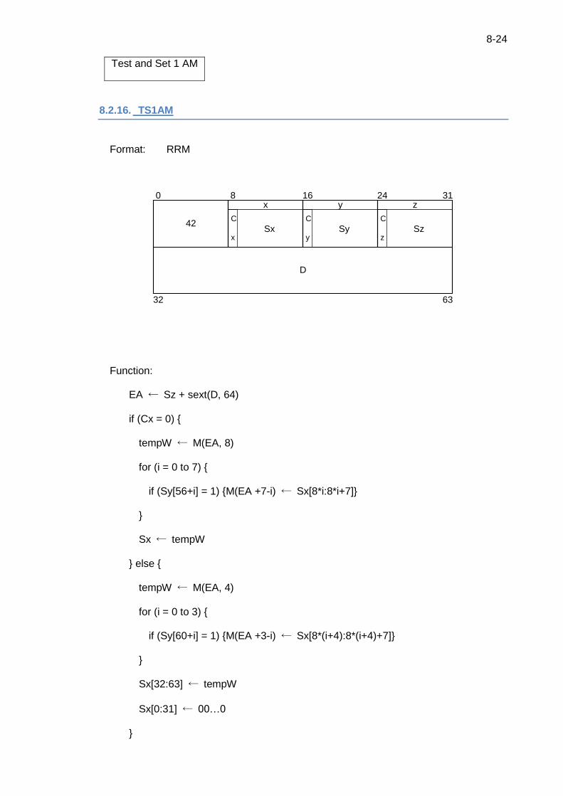
8-24
Test and Set 1 AM
8.2.16. TS1AM
Format: RRM
x
42 Sx Sy Sz
y
C
y
z
C
z
8 16 24 31
32 63
0
C
x
D
Function:
EA ← Sz + sext(D, 64)
if (Cx = 0) {
tempW ← M(EA, 8)
for (i = 0 to 7) {
if (Sy[56+i] = 1) {M(EA +7-i) ← Sx[8*i:8*i+7]}
}
Sx ← tempW
} else {
tempW ← M(EA, 4)
for (i = 0 to 3) {
if (Sy[60+i] = 1) {M(EA +3-i) ← Sx[8*(i+4):8*(i+4)+7]}
}
Sx[32:63] ← tempW
Sx[0:31] ← 00…0
}
8-25
Case of Cx=0:
The 8-byte data starting at the EA designated by z and D fields is replaced by the
contents of the Sx register according to bit [56:63] of the Sy register or immediate value
specified by the y field.
Sy[56:63] corresponds to the eight byte target in the memory and 8-byte data of Sx. The
Sy[56] corresponds to the lowest byte of memory and the highest byte of Sx, oppositely
Sy[63] is to the highest byte of memory and the lowest byte of Sx.
Each byte in Sx that its corresponding bit in Sy[56:63] is 1, is stored in the
corresponding byte position of memory. The content of the memory byte with its
corresponding bit=0 remains unchanged.
The EA address specified by Sz and D must be aligned to an 8byte boundary. If bits 61,
62 and 63 of EA are not zero, a memory access exception is generated.
8-26
Case of Cx=1:
The individual 4-byte data starting at the location designated by z and D fields is
replaced the contents of the S register specified in the x fields, according to bit[60:63] of
the Sy register or immediate value specified in the y field.
Sy[60:63] corresponds to the four byte target in the memory and 4-byte data of Sx. The
Sy[60] corresponds to the lowest byte of memory and the highest byte of Sx, oppositely
Sy[63] is to the highest byte of memory and the lowest byte of Sx.
Each byte in Sx that its corresponding bit in Sy[60:63] is 1, is stored in the
corresponding byte position of memory. The content of the memory byte with its
corresponding bit=0 remains unchanged.
The original memory data (before this operation) is loaded into Sx.
The address indicated by Sz must be aligned to a 4byte boundary. If bits 62 and 63 of
Sz are not zero, a memory access exception is generated.
Exceptions:
・Memory protection exception
・Missing page exception
・Missing space exception
・Memory access exception
・Address match interrupt
Notes:
・Atomicity for this operation is guaranteed. Following instructions cannot access the
target address before the TS1AM has completed.
・When Cz=0, z operand is immediate 0 regardless of Sz value.
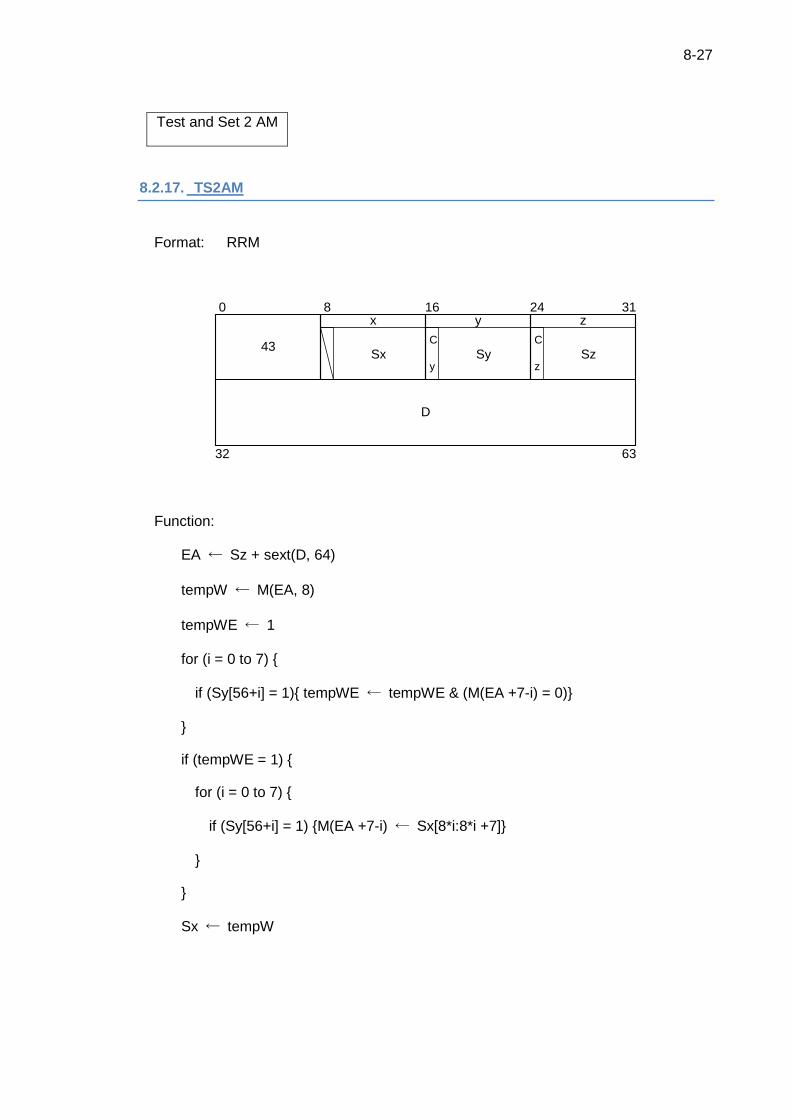
8-27
Test and Set 2 AM
8.2.17. TS2AM
Format: RRM
x
43 Sx Sy Sz
y
C
y
z
C
z
8 16 24 31
32 63
0
D
Function:
EA ← Sz + sext(D, 64)
tempW ← M(EA, 8)
tempWE ← 1
for (i = 0 to 7) {
if (Sy[56+i] = 1){ tempWE ← tempWE & (M(EA +7-i) = 0)}
}
if (tempWE = 1) {
for (i = 0 to 7) {
if (Sy[56+i] = 1) {M(EA +7-i) ← Sx[8*i:8*i +7]}
}
}
Sx ← tempW
8-28
The 8-byte memory data starting at the location designated by the S register or the
immediate value specified in the z field is loaded into the Sx register. According to bits 56
to 63 of the y operand (Sy register or immediate value specified in the y field) and the
memory data, corresponding Sx register data is written to the memory.
The bits of Sy[56:63] correspond to the eight bytes of memory and 8-byte data of Sx.
Sy[56] corresponds to the lowest byte of memory and highest byte of Sx. Oppositely
Sy[63] corresponds to the highest byte of memory and the lowest byte of Sx.
Write to the memory happens when all memory bytes corresponding to 1s in Sy[56:63]
are all zero. For example, if Sy[56] and Sy[57] are one but the second lowest byte is not
zero, write to both bytes won’t occur. When Sy[56:63] are all zero, the target memory
contents also stay unchanged.
If the condition is met, Sx are bytewise written to the corresponding byte location in the
memory, according to Sy[56:63] . In the previous example, when Sy[56] and Sy[57] are
one and the others are all zero, and the first and second lowest bytes are zero, Sx’s first
and second highest bytes are written to the first and second lowest bytes in the target
memory respectively. In that case the other target memory bytes stay unchanged.
The original memory data (before this instruction is operated) is stored in Sx.
The EA address indicated by Sz and D must be aligned to an 8byte boundary. If bits 61
to 63 of EA are not zeros, then a memory access exception is generated.
8-29
Exceptions:
・Memory protection exception
・Missing page exception
・Missing space exception
・Memory access exception
・Address match interrupt
Notes:
・TS1AM remark description also applies.
・When Cz=0, z operand is immediate 0 regardless of Sz value.
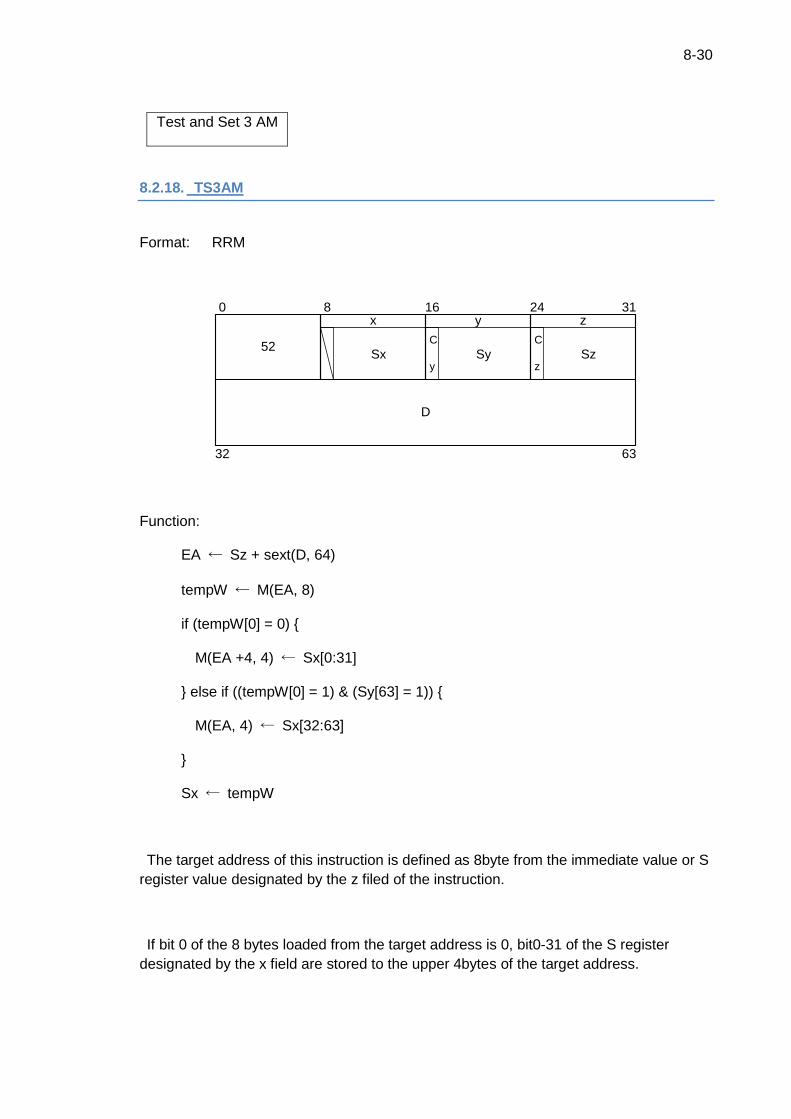
8-30
Test and Set 3 AM
8.2.18. TS3AM
Format: RRM
x
52 Sx Sy Sz
y
C
y
z
C
z
8 16 24 31
32 63
0
D
Function:
EA ← Sz + sext(D, 64)
tempW ← M(EA, 8)
if (tempW[0] = 0) {
M(EA +4, 4) ← Sx[0:31]
} else if ((tempW[0] = 1) & (Sy[63] = 1)) {
M(EA, 4) ← Sx[32:63]
}
Sx ← tempW
The target address of this instruction is defined as 8byte from the immediate value or S
register value designated by the z filed of the instruction.
If bit 0 of the 8 bytes loaded from the target address is 0, bit0-31 of the S register
designated by the x field are stored to the upper 4bytes of the target address.
8-31
If bit 0 of the 8 bytes loaded from the target address is 1 and Sy[63] is 1, bits 32-63 of
the S register designated by the x field are stored to the lower 4bytes of the target
address.
The original 8 byte memory data (before the modification) is stored in the S register
designated by the x field.
The EA address indicated by Sz and D must be aligned to an 8-byte boundary. If bits 61
to 63 of EA are not zeros, a memory access exception is generated.
Exceptions:
・Memory protection exception
・Missing page exception
・Missing space exception
・Memory access exception
・Address match interrupt
Notes:
・TS1AM remark description also applies.
・When Cz=0, z operand is immediate 0 regardless of Sz value.
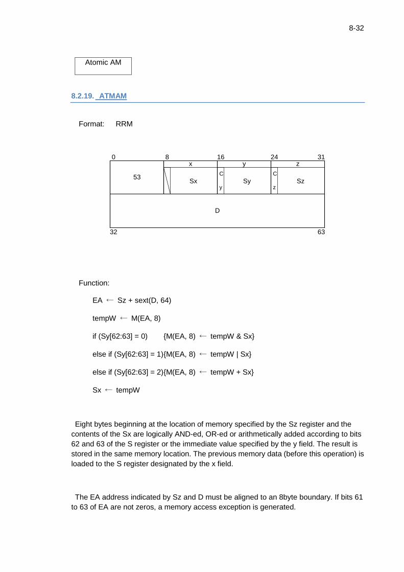
8-32
Atomic AM
8.2.19. ATMAM
Format: RRM
x
53 Sx Sy Sz
y
C
y
z
C
z
8 16 24 31
32 63
0
D
Function:
EA ← Sz + sext(D, 64)
tempW ← M(EA, 8)
if (Sy[62:63] = 0) {M(EA, 8) ← tempW & Sx}
else if (Sy[62:63] = 1) {M(EA, 8) ← tempW | Sx}
else if (Sy[62:63] = 2) {M(EA, 8) ← tempW + Sx}
Sx ← tempW
Eight bytes beginning at the location of memory specified by the Sz register and the
contents of the Sx are logically AND-ed, OR-ed or arithmetically added according to bits
62 and 63 of the S register or the immediate value specified by the y field. The result is
stored in the same memory location. The previous memory data (before this operation) is
loaded to the S register designated by the x field.
The EA address indicated by Sz and D must be aligned to an 8byte boundary. If bits 61
to 63 of EA are not zeros, a memory access exception is generated.
8-33
Exceptions:
・Memory protection exception
・Missing page exception
・Missing space exception
・Memory access exception
・Address match interrupt
Notes:
・TS1AM remark description also applies.
・Sy should not be set to 3, while hardware may treat it as Sy=2.
・When Cz=0, z operand is immediate 0 regardless Sz value.
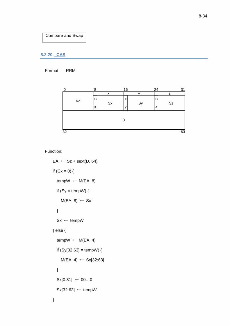
8-34
Compare and Swap
8.2.20. CAS
Format: RRM
x
62 Sx Sy Sz
y
C
y
z
C
z
8 16 24 31
32 63
0
C
x
D
Function:
EA ← Sz + sext(D, 64)
if (Cx = 0) {
tempW ← M(EA, 8)
if (Sy = tempW) {
M(EA, 8) ← Sx
}
Sx ← tempW
} else {
tempW ← M(EA, 4)
if (Sy[32:63] = tempW) {
M(EA, 4) ← Sx[32:63]
}
Sx[0:31] ← 00…0
Sx[32:63] ← tempW
}
8-35
When Cx=0, the 8-byte data at the location designated by the Sz, and the contents of Sy
are compared. If they are matched, the 8byte contents of Sx are stored into the memory
space designated by Sz and D. Regardless of the comparison result, the memory data
before this operation is loaded to Sx.
The address specified by Sz and D must be aligned to an 8-byte boundary. If bits 61 to
63 of Sz are not zeros, a memory access exception is generated.
When Cx=1, the 4byte data at the location designated by the Sz, and the contents of Sy
bit32-63 are compared. If they are matched, the contents of Sx bit32-63 are stored into
the memory designated by Sz and D. Regardless the comparison result, the memory
data before this operation loaded to the lower 4bytes of Sx, and the upper 4bytes of Sx
are filled with zeros.
The EA address specified by Sz and D must be aligned to a 4-byte boundary. If bits 62
and 63 of EA are not zeros, a memory access exception is generated.
The comparison result of the data in the EA address and Sy is not given. To obtain it,
another comparison between Sx and Sy is required.
Exceptions:
・Memory protection exception
・Missing page exception
・Missing space exception
・Memory access exception
・Address match interrupt
Notes:
・Refer to TS1AM.
・When Cz=0, z operand is an immediate 0 regardless of Sz.
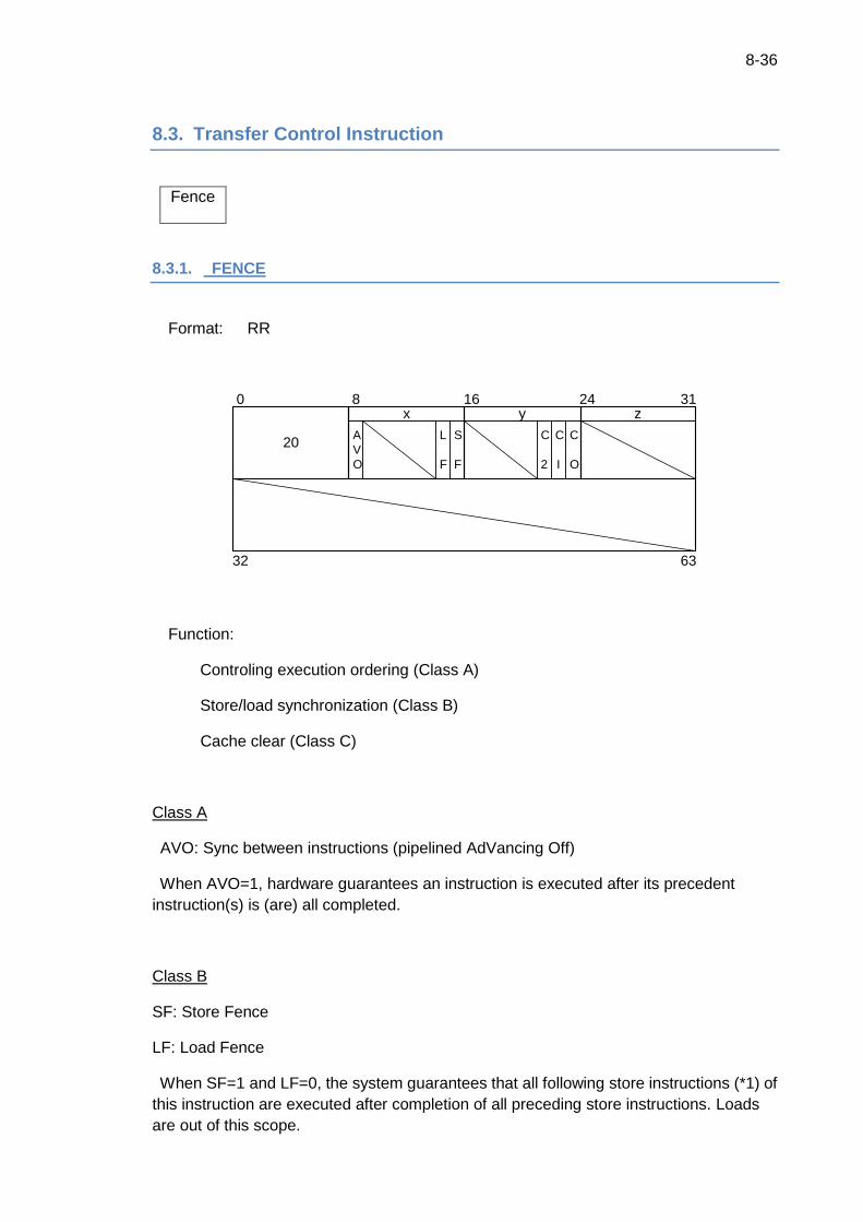
8-36
8.3. Transfer Control Instruction
Fence
8.3.1. FENCE
Format: RR
x
20
y z8 16 24 31
32 63
0
S
F
L
F
A
V
O
C
O
C
I
C
2
Function:
Controling execution ordering (Class A)
Store/load synchronization (Class B)
Cache clear (Class C)
Class A
AVO: Sync between instructions (pipelined AdVancing Off)
When AVO=1, hardware guarantees an instruction is executed after its precedent
instruction(s) is (are) all completed.
Class B
SF: Store Fence
LF: Load Fence
When SF=1 and LF=0, the system guarantees that all following store instructions (*1) of
this instruction are executed after completion of all preceding store instructions. Loads
are out of this scope.
8-37
When SF=0 and LF=1, the system guarantees that all following load instructions (*2) of
this instruction are executed after completion of all preceding load instructions of this
instruction. Stores are out of this scope.
When SF=1 and LF=1, the system guarantees that all following store and load
instructions of this instruction are executed after completion of all preceding store and
load instructions of this instruction.
Class C
CI, CO and C2:
When CI=1, the scalar instruction cache is cleared.
When CO=1, the scalar operand cache is cleared.
When C2=1, the scalar L2 is cleared.
A single FENCE instruction should include control bits that belong to a single class.
Otherwise, it may cause an unexpected result.
Exceptions: None
8-38
Notes:
・*1 instructions: STS, STU, STL, ST1B, ST2B, VST, VSTU, VSTL, VST2D, VSTU2D,
VSTL2D, VSC, VSCU, VSCL, TS1AM, TS2AM, TS3AM, ATMAM,
CAS, SCR, TSCR, FIDCR, SHM
・*2 instructions: LDS, LDU, LDL, LD1B, LD2B, DLDS, DLDU, DLDL, PFCH, VLD,
VLDU, VLDL, VLD2D, VLDU2D, VLDL2D, VGT, VGTU, VGTL,
TS1AM, TS2AM, TS3AM, ATMAM, CAS, LCR, TSCR, FIDCR,
LHM
・ Note: instruction codes loaded in the S cache or being executed are not affected
by memory writes by cores or the DMA engine, even when their write is to the
memory area including the instruction codes. To avoid such inconsistency
between S cache and the memory, FENCE instruction should be executed
properly.
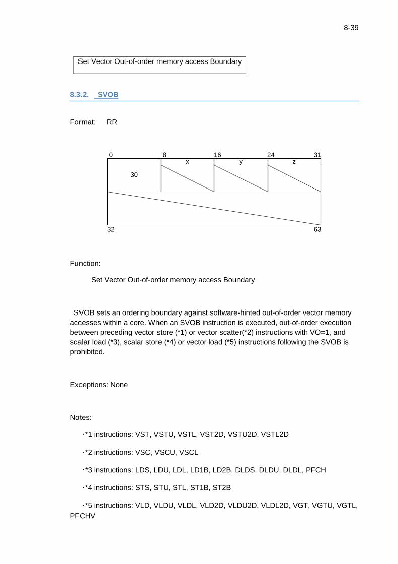
8-39
Set Vector Out-of-order memory access Boundary
8.3.2. SVOB
Format: RR
x
30
y z8 16 24 31
32 63
0
Function:
Set Vector Out-of-order memory access Boundary
SVOB sets an ordering boundary against software-hinted out-of-order vector memory
accesses within a core. When an SVOB instruction is executed, out-of-order execution
between preceding vector store (*1) or vector scatter(*2) instructions with VO=1, and
scalar load (*3), scalar store (*4) or vector load (*5) instructions following the SVOB is
prohibited.
Exceptions: None
Notes:
・*1 instructions: VST, VSTU, VSTL, VST2D, VSTU2D, VSTL2D
・*2 instructions: VSC, VSCU, VSCL
・*3 instructions: LDS, LDU, LDL, LD1B, LD2B, DLDS, DLDU, DLDL, PFCH
・*4 instructions: STS, STU, STL, ST1B, ST2B
・*5 instructions: VLD, VLDU, VLDL, VLD2D, VLDU2D, VLDL2D, VGT, VGTU, VGTL,
PFCHV

8-40
・Refer to chapter of VST, VSTU, VSTL, VST2D, VSTU2D, VSTL2D, VSC, VSCU
and VSCL.
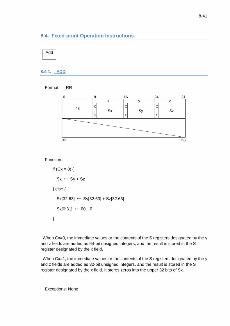
8-41
8.4. Fixed-point Operation Instructions
Add
8.4.1. ADD
Format: RR
x
48 Sx Sy Sz
y
C
y
z
C
z
8 16 24 31
32 63
0
C
x
Function:
if (Cx = 0) {
Sx ← Sy + Sz
} else {
Sx[32:63] ← Sy[32:63] + Sz[32:63]
Sx[0:31] ← 00…0
}
When Cx=0, the immediate values or the contents of the S registers designated by the y
and z fields are added as 64-bit unsigned integers, and the result is stored in the S
register designated by the x field.
When Cx=1, the immediate values or the contents of the S registers designated by the y
and z fields are added as 32-bit unsigned integers, and the result is stored in the S
register designated by the x field. It stores zeros into the upper 32 bits of Sx.
Exceptions: None
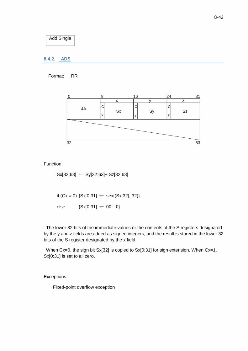
8-42
Add Single
8.4.2. ADS
Format: RR
C
x
x
4A Sx Sy Sz
y
C
y
z
C
z
8 16 24 31
32 63
0
Function:
Sx[32:63] ← Sy[32:63]+ Sz[32:63]
if (Cx = 0) {Sx[0:31] ← sext(Sx[32], 32)}
else {Sx[0:31] ← 00…0}
The lower 32 bits of the immediate values or the contents of the S registers designated
by the y and z fields are added as signed integers, and the result is stored in the lower 32
bits of the S register designated by the x field.
When Cx=0, the sign bit Sx[32] is copied to Sx[0:31] for sign extension. When Cx=1,
Sx[0:31] is set to all zero.
Exceptions:
・Fixed-point overflow exception
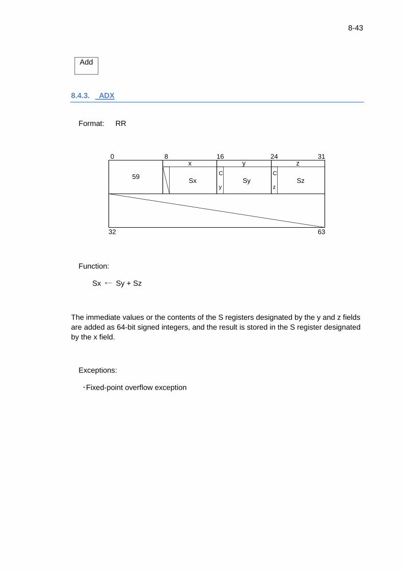
8-43
Add
8.4.3. ADX
Format: RR
x
59 Sx Sy Sz
y
C
y
z
C
z
8 16 24 31
32 63
0
Function:
Sx ← Sy + Sz
The immediate values or the contents of the S registers designated by the y and z fields
are added as 64-bit signed integers, and the result is stored in the S register designated
by the x field.
Exceptions:
・Fixed-point overflow exception
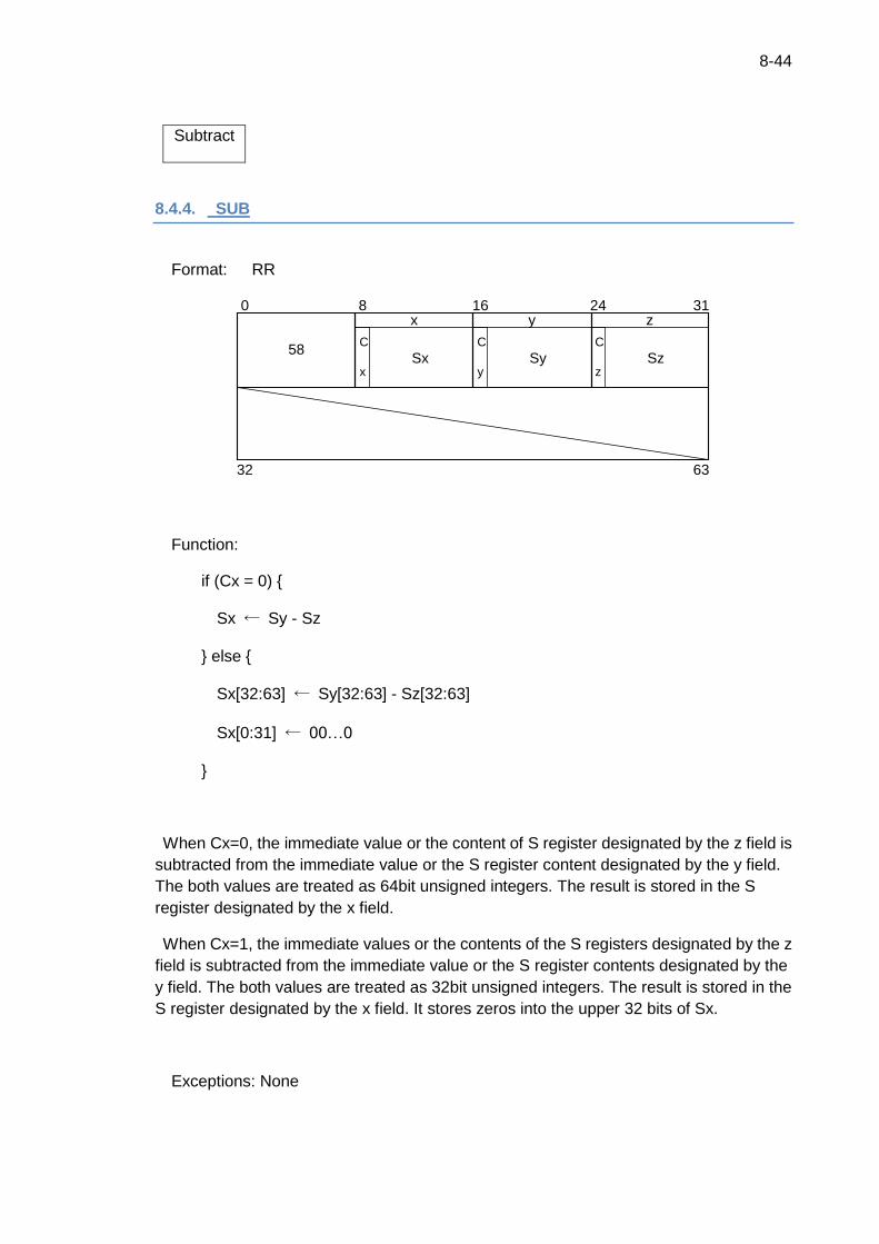
8-44
Subtract
8.4.4. SUB
Format: RR
x
58 Sx Sy Sz
y
C
y
z
C
z
8 16 24 31
32 63
0
C
x
Function:
if (Cx = 0) {
Sx ← Sy - Sz
} else {
Sx[32:63] ← Sy[32:63] - Sz[32:63]
Sx[0:31] ← 00…0
}
When Cx=0, the immediate value or the content of S register designated by the z field is
subtracted from the immediate value or the S register content designated by the y field.
The both values are treated as 64bit unsigned integers. The result is stored in the S
register designated by the x field.
When Cx=1, the immediate values or the contents of the S registers designated by the z
field is subtracted from the immediate value or the S register contents designated by the
y field. The both values are treated as 32bit unsigned integers. The result is stored in the
S register designated by the x field. It stores zeros into the upper 32 bits of Sx.
Exceptions: None
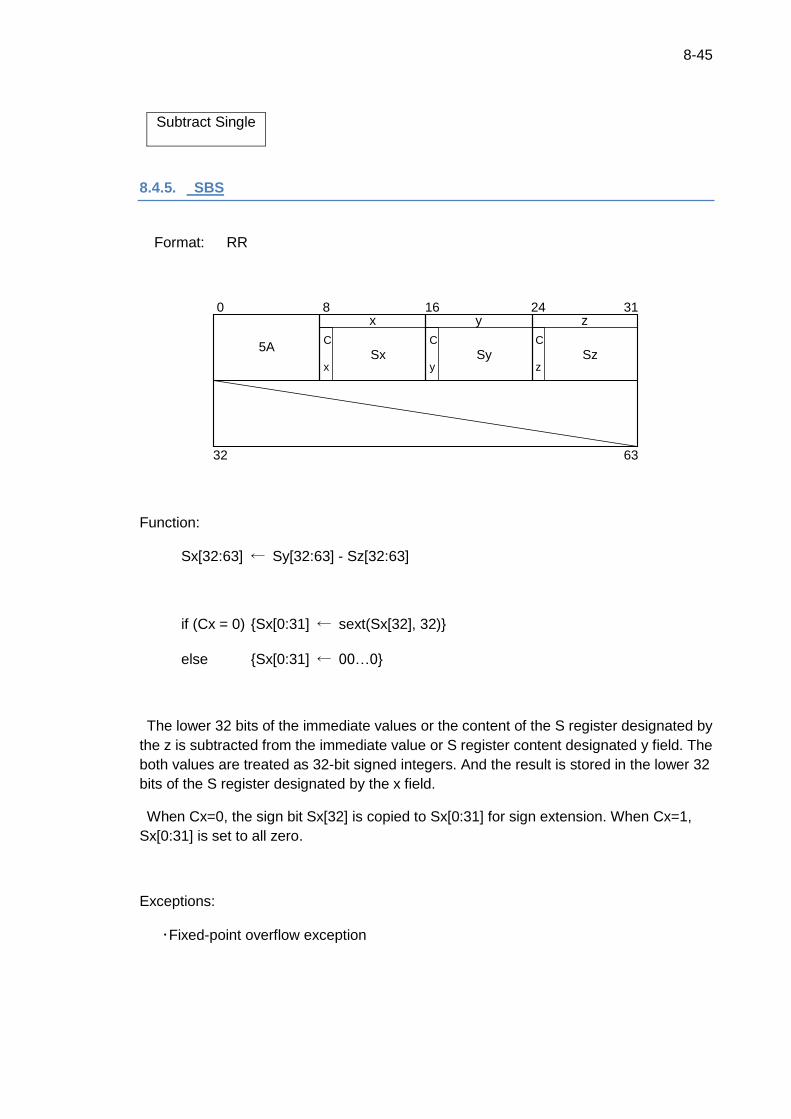
8-45
Subtract Single
8.4.5. SBS
Format: RR
x
5A Sx Sy Sz
y
C
y
z
C
z
8 16 24 31
32 63
0
C
x
Function:
Sx[32:63] ← Sy[32:63] - Sz[32:63]
if (Cx = 0) {Sx[0:31] ← sext(Sx[32], 32)}
else {Sx[0:31] ← 00…0}
The lower 32 bits of the immediate values or the content of the S register designated by
the z is subtracted from the immediate value or S register content designated y field. The
both values are treated as 32-bit signed integers. And the result is stored in the lower 32
bits of the S register designated by the x field.
When Cx=0, the sign bit Sx[32] is copied to Sx[0:31] for sign extension. When Cx=1,
Sx[0:31] is set to all zero.
Exceptions:
・Fixed-point overflow exception
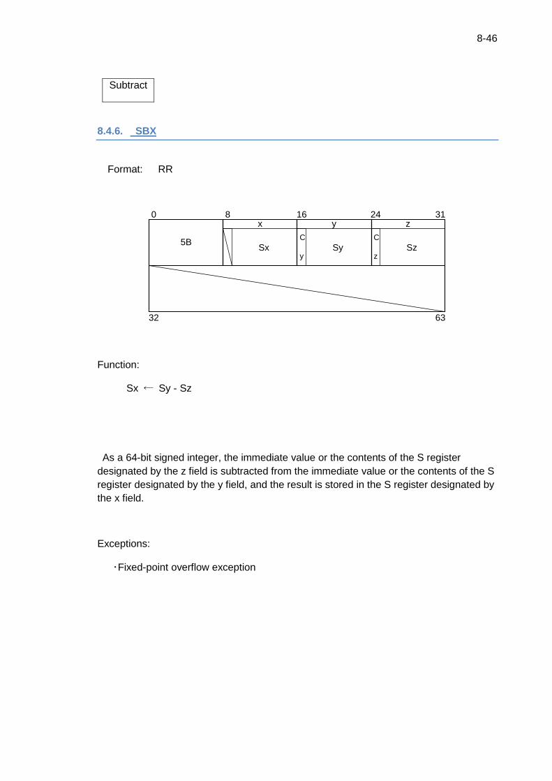
8-46
Subtract
8.4.6. SBX
Format: RR
x
5B Sx Sy Sz
y
C
y
z
C
z
8 16 24 31
32 63
0
Function:
Sx ← Sy - Sz
As a 64-bit signed integer, the immediate value or the contents of the S register
designated by the z field is subtracted from the immediate value or the contents of the S
register designated by the y field, and the result is stored in the S register designated by
the x field.
Exceptions:
・Fixed-point overflow exception
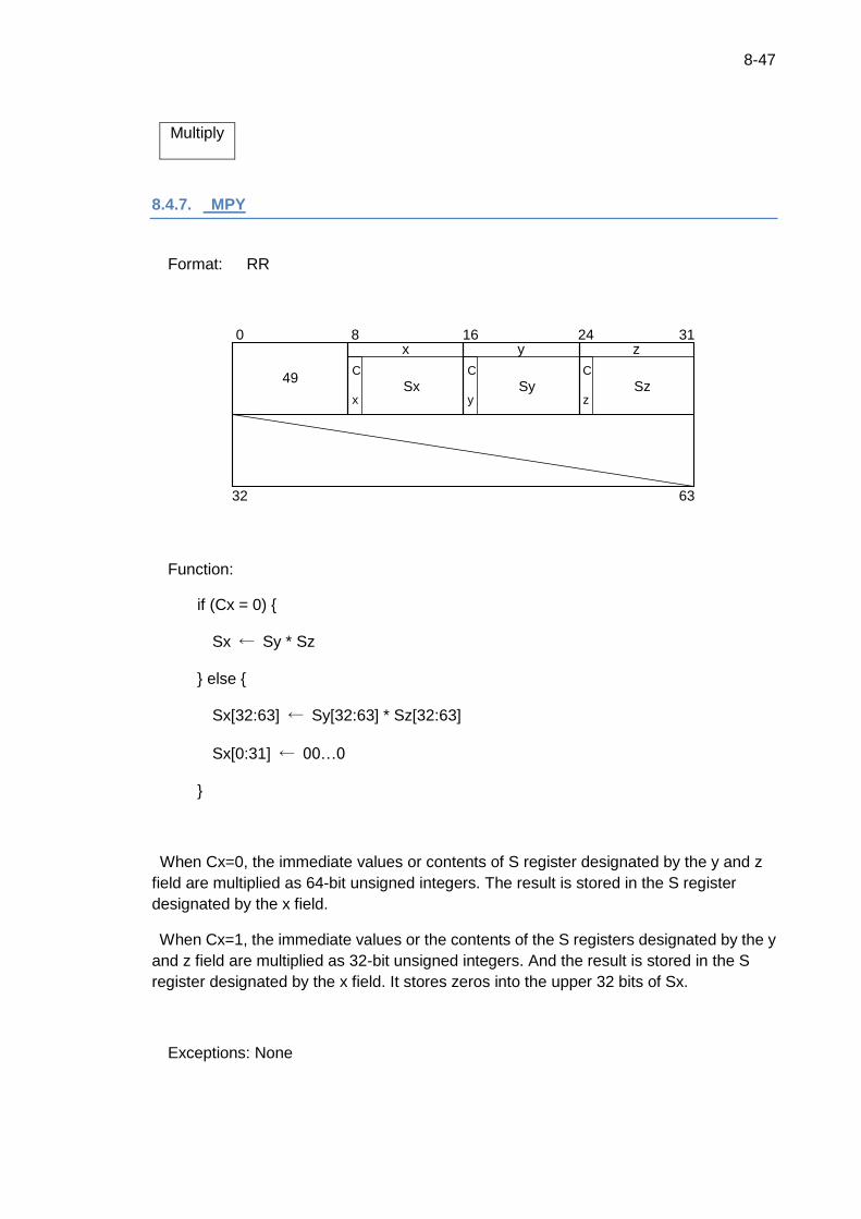
8-47
Multiply
8.4.7. MPY
Format: RR
x
49 Sx Sy Sz
y
C
y
z
C
z
8 16 24 31
32 63
0
C
x
Function:
if (Cx = 0) {
Sx ← Sy * Sz
} else {
Sx[32:63] ← Sy[32:63] * Sz[32:63]
Sx[0:31] ← 00…0
}
When Cx=0, the immediate values or contents of S register designated by the y and z
field are multiplied as 64-bit unsigned integers. The result is stored in the S register
designated by the x field.
When Cx=1, the immediate values or the contents of the S registers designated by the y
and z field are multiplied as 32-bit unsigned integers. And the result is stored in the S
register designated by the x field. It stores zeros into the upper 32 bits of Sx.
Exceptions: None
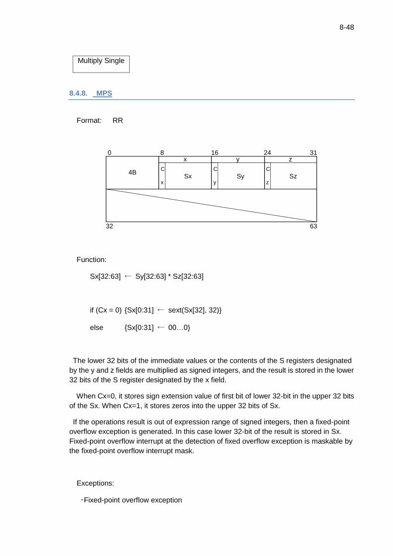
8-48
Multiply Single
8.4.8. MPS
Format: RR
x
4B Sx Sy Sz
y
C
y
z
C
z
8 16 24 31
32 63
0
C
x
Function:
Sx[32:63] ← Sy[32:63] * Sz[32:63]
if (Cx = 0) {Sx[0:31] ← sext(Sx[32], 32)}
else {Sx[0:31] ← 00…0}
The lower 32 bits of the immediate values or the contents of the S registers designated
by the y and z fields are multiplied as signed integers, and the result is stored in the lower
32 bits of the S register designated by the x field.
When Cx=0, it stores sign extension value of first bit of lower 32-bit in the upper 32 bits
of the Sx. When Cx=1, it stores zeros into the upper 32 bits of Sx.
If the operations result is out of expression range of signed integers, then a fixed-point
overflow exception is generated. In this case lower 32-bit of the result is stored in Sx.
Fixed-point overflow interrupt at the detection of fixed overflow exception is maskable by
the fixed-point overflow interrupt mask.
Exceptions:
・Fixed-point overflow exception
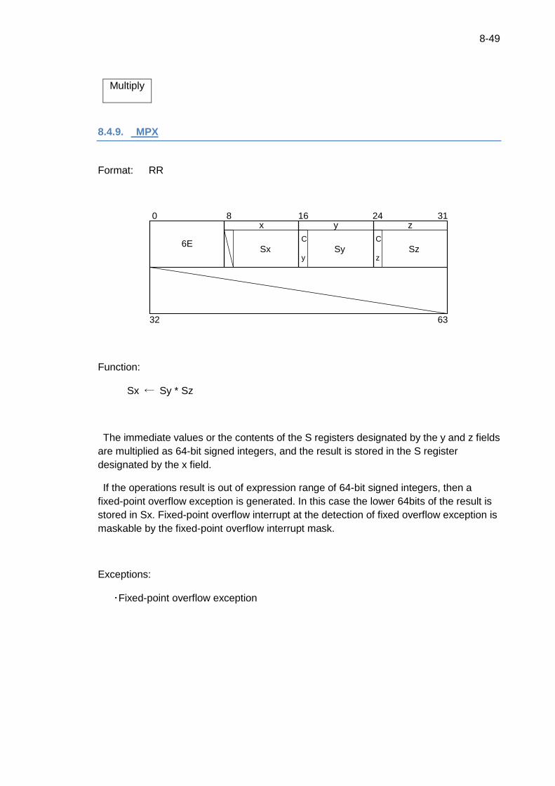
8-49
Multiply
8.4.9. MPX
Format: RR
x
6E Sx Sy Sz
y
C
y
z
C
z
8 16 24 31
32 63
0
Function:
Sx ← Sy * Sz
The immediate values or the contents of the S registers designated by the y and z fields
are multiplied as 64-bit signed integers, and the result is stored in the S register
designated by the x field.
If the operations result is out of expression range of 64-bit signed integers, then a
fixed-point overflow exception is generated. In this case the lower 64bits of the result is
stored in Sx. Fixed-point overflow interrupt at the detection of fixed overflow exception is
maskable by the fixed-point overflow interrupt mask.
Exceptions:
・Fixed-point overflow exception
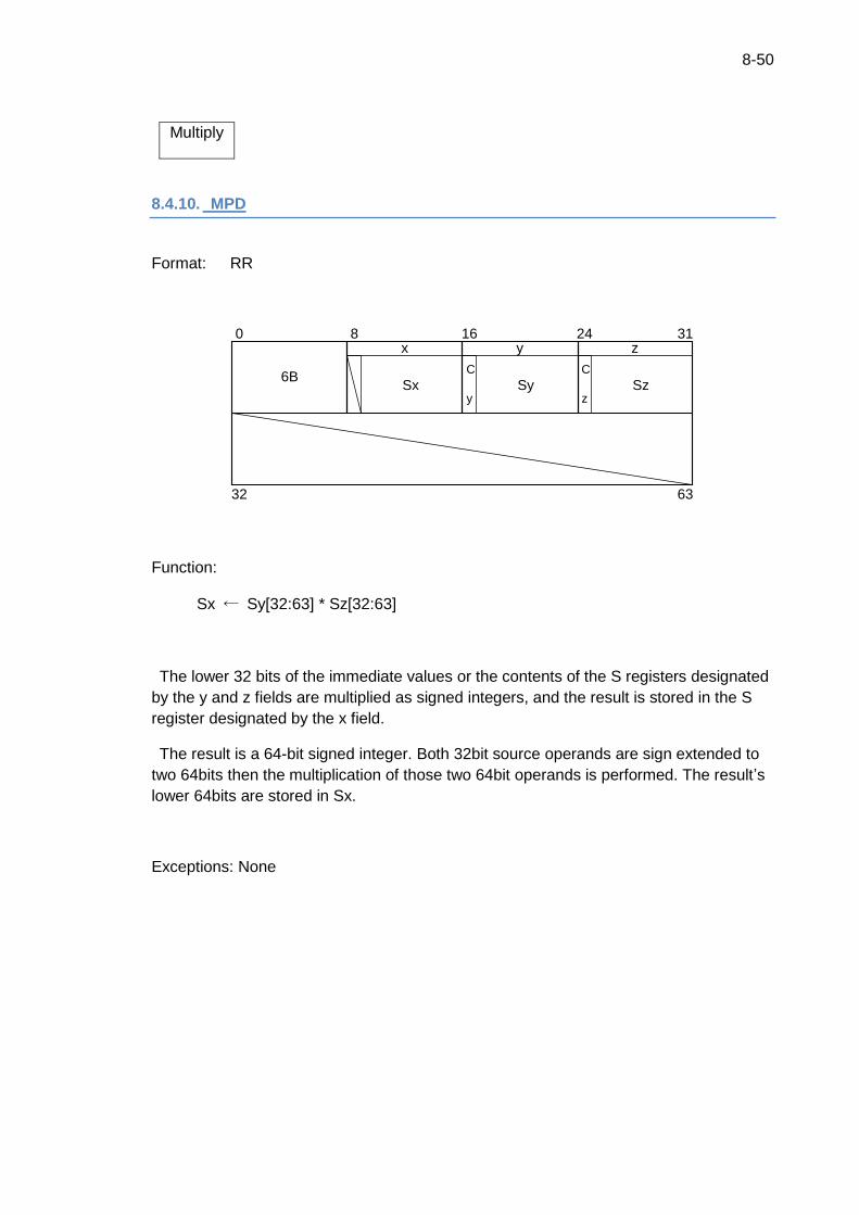
8-50
Multiply
8.4.10. MPD
Format: RR
x
6B Sx Sy Sz
y
C
y
z
C
z
8 16 24 31
32 63
0
Function:
Sx ← Sy[32:63] * Sz[32:63]
The lower 32 bits of the immediate values or the contents of the S registers designated
by the y and z fields are multiplied as signed integers, and the result is stored in the S
register designated by the x field.
The result is a 64-bit signed integer. Both 32bit source operands are sign extended to
two 64bits then the multiplication of those two 64bit operands is performed. The result’s
lower 64bits are stored in Sx.
Exceptions: None
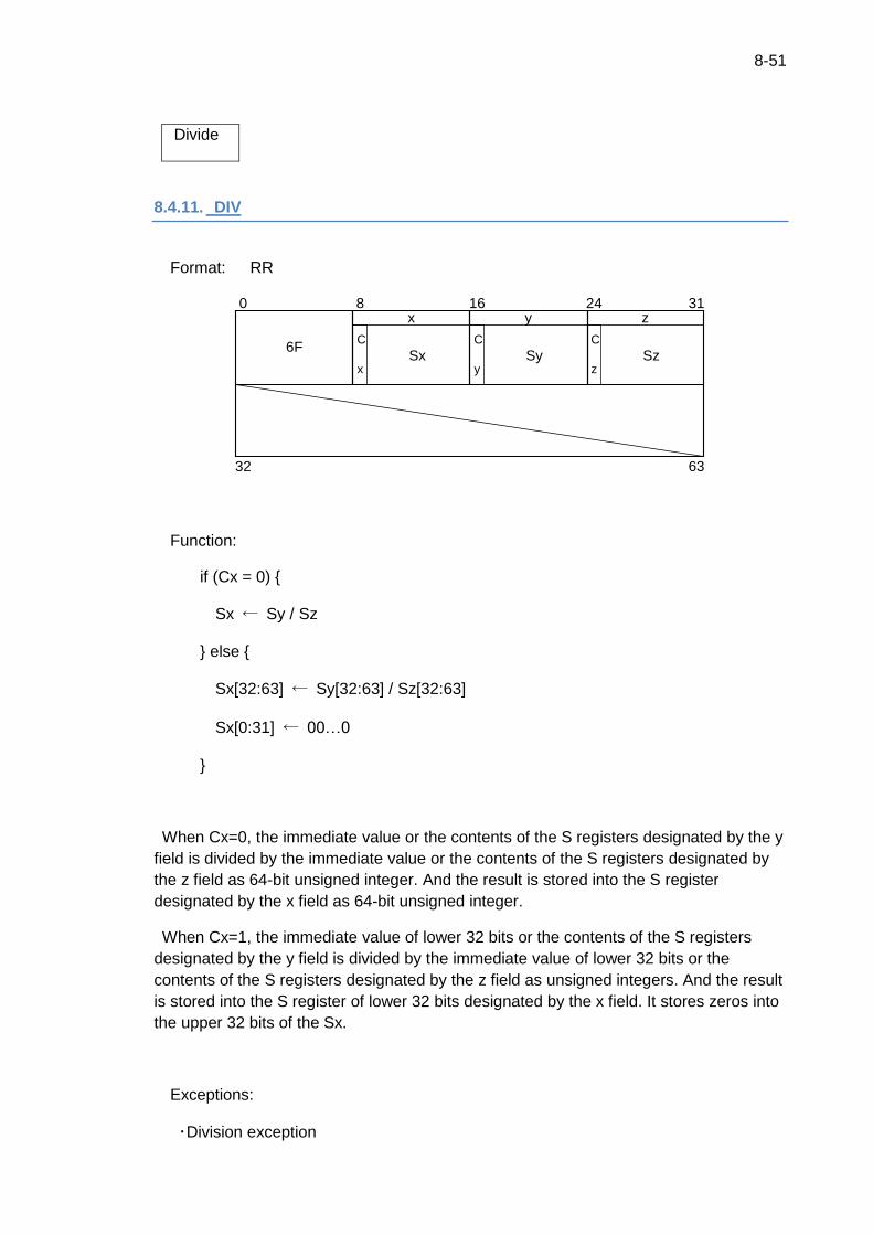
8-51
Divide
8.4.11. DIV
Format: RR
x
6F Sx Sy Sz
y
C
y
z
C
z
8 16 24 31
32 63
0
C
x
Function:
if (Cx = 0) {
Sx ← Sy / Sz
} else {
Sx[32:63] ← Sy[32:63] / Sz[32:63]
Sx[0:31] ← 00…0
}
When Cx=0, the immediate value or the contents of the S registers designated by the y
field is divided by the immediate value or the contents of the S registers designated by
the z field as 64-bit unsigned integer. And the result is stored into the S register
designated by the x field as 64-bit unsigned integer.
When Cx=1, the immediate value of lower 32 bits or the contents of the S registers
designated by the y field is divided by the immediate value of lower 32 bits or the
contents of the S registers designated by the z field as unsigned integers. And the result
is stored into the S register of lower 32 bits designated by the x field. It stores zeros into
the upper 32 bits of the Sx.
Exceptions:
・Division exception
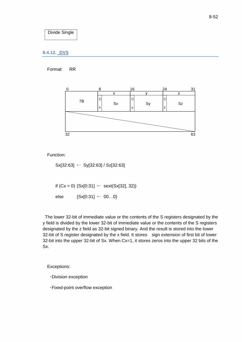
8-52
Divide Single
8.4.12. DVS
Format: RR
x
7B Sx Sy Sz
y
C
y
z
C
z
8 16 24 31
32 63
0
C
x
Function:
Sx[32:63] ← Sy[32:63] / Sz[32:63]
if (Cx = 0) {Sx[0:31] ← sext(Sx[32], 32)}
else {Sx[0:31] ← 00…0}
The lower 32-bit of immediate value or the contents of the S registers designated by the
y field is divided by the lower 32-bit of immediate value or the contents of the S registers
designated by the z field as 32-bit signed binary. And the result is stored into the lower
32-bit of S register designated by the x field. It stores sign extension of first bit of lower
32-bit into the upper 32-bit of Sx. When Cx=1, it stores zeros into the upper 32 bits of the
Sx.
Exceptions:
・Division exception
・Fixed-point overflow exception
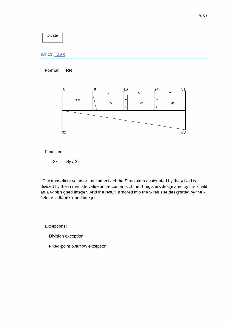
8-53
Divide
8.4.13. DVX
Format: RR
x
7F Sx Sy Sz
y
C
y
z
C
z
8 16 24 31
32 63
0
Function:
Sx ← Sy / Sz
The immediate value or the contents of the S registers designated by the y field is
divided by the immediate value or the contents of the S registers designated by the z field
as a 64bit signed integer. And the result is stored into the S register designated by the x
field as a 64bit signed integer.
Exceptions:
・Division exception
・Fixed-point overflow exception
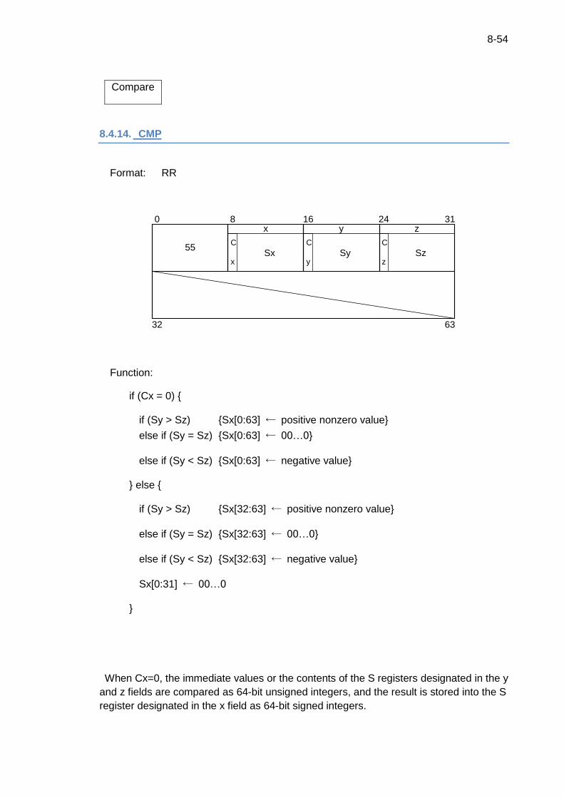
8-54
Compare
8.4.14. CMP
Format: RR
x
55 Sx Sy Sz
y
C
y
z
C
z
8 16 24 31
32 63
0
C
x
Function:
if (Cx = 0) {
if (Sy > Sz) {Sx[0:63] ← positive nonzero value}
else if (Sy = Sz) {Sx[0:63] ← 00…0}
else if (Sy < Sz) {Sx[0:63] ← negative value}
} else {
if (Sy > Sz) {Sx[32:63] ← positive nonzero value}
else if (Sy = Sz) {Sx[32:63] ← 00…0}
else if (Sy < Sz) {Sx[32:63] ← negative value}
Sx[0:31] ← 00…0
}
When Cx=0, the immediate values or the contents of the S registers designated in the y
and z fields are compared as 64-bit unsigned integers, and the result is stored into the S
register designated in the x field as 64-bit signed integers.
8-55
If Sy>Sz, a positive nonzero value is stored to Sx.
If Sy=Sz, zero is stored to Sx.
If Sy<Sz, a negative nonzero value is stored to Sx.
When Cx=1, the immediate 32bit values or the contents of the S registers designated in
the y and z fields are compared as unsigned integers, and the result is stored into the S
register designated in the x field as 32-bit signed integers. It stores zeros into the upper
32 bits of the Sx.
If Sy>Sz, a positive nonzero value is stored to the bit 32-63 of Sx.
If Sy=Sz, zero is stored to the bit 32-63 of Sx.
If Sy<Sz, a negative nonzero value is stored to the bit 32-63 of Sx.
In any case, no fixed-point overflow exception occurs with regardless of the value of the
exception mask.
Exceptions: None
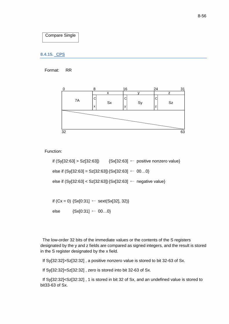
8-56
Compare Single
8.4.15. CPS
Format: RR
x
7A Sx Sy Sz
y
C
y
z
C
z
8 16 24 31
32 63
0
C
x
Function:
if (Sy[32:63] > Sz[32:63]) {Sx[32:63] ← positive nonzero value}
else if (Sy[32:63] = Sz[32:63]) {Sx[32:63] ← 00…0}
else if (Sy[32:63] < Sz[32:63]) {Sx[32:63] ← negative value}
if (Cx = 0) {Sx[0:31] ← sext(Sx[32], 32)}
else {Sx[0:31] ← 00…0}
The low-order 32 bits of the immediate values or the contents of the S registers
designated by the y and z fields are compared as signed integers, and the result is stored
in the S register designated by the x field.
If Sy[32:32]>Sz[32:32] , a positive nonzero value is stored to bit 32-63 of Sx.
If Sy[32:32]=Sz[32:32] , zero is stored into bit 32-63 of Sx.
If Sy[32:32]<Sz[32:32] , 1 is stored in bit 32 of Sx, and an undefined value is stored to
bit33-63 of Sx.
8-57
When Cx=0, Sx[32] is copied to the upper 32 bits of the Sx for sign extension. When
Cx=1, zeros are stored to the upper 32 bits of the Sx.
In any case, no fixed-point overflow exception occurs irrespective of the value of the
exception mask.
Exceptions: None
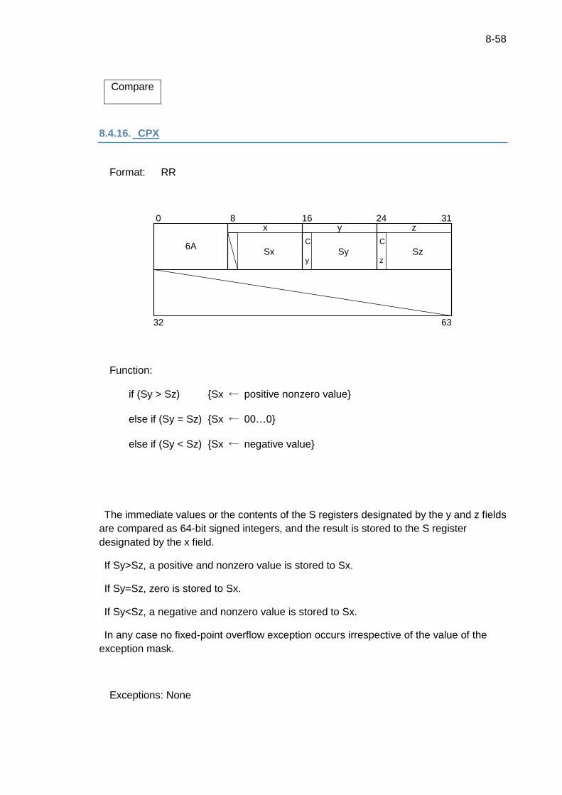
8-58
Compare
8.4.16. CPX
Format: RR
x
6A Sx Sy Sz
y
C
y
z
C
z
8 16 24 31
32 63
0
Function:
if (Sy > Sz) {Sx ← positive nonzero value}
else if (Sy = Sz) {Sx ← 00…0}
else if (Sy < Sz) {Sx ← negative value}
The immediate values or the contents of the S registers designated by the y and z fields
are compared as 64-bit signed integers, and the result is stored to the S register
designated by the x field.
If Sy>Sz, a positive and nonzero value is stored to Sx.
If Sy=Sz, zero is stored to Sx.
If Sy<Sz, a negative and nonzero value is stored to Sx.
In any case no fixed-point overflow exception occurs irrespective of the value of the
exception mask.
Exceptions: None
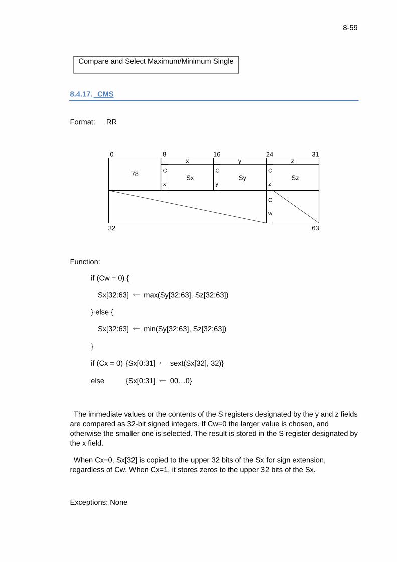
8-59
Compare and Select Maximum/Minimum Single
8.4.17. CMS
Format: RR
x
78 Sx Sy Sz
y
C
y
z
C
z
8 16 24 31
32 63
0
C
x
C
w
Function:
if (Cw = 0) {
Sx[32:63] ← max(Sy[32:63], Sz[32:63])
} else {
Sx[32:63] ← min(Sy[32:63], Sz[32:63])
}
if (Cx = 0) {Sx[0:31] ← sext(Sx[32], 32)}
else {Sx[0:31] ← 00…0}
The immediate values or the contents of the S registers designated by the y and z fields
are compared as 32-bit signed integers. If Cw=0 the larger value is chosen, and
otherwise the smaller one is selected. The result is stored in the S register designated by
the x field.
When Cx=0, Sx[32] is copied to the upper 32 bits of the Sx for sign extension,
regardless of Cw. When Cx=1, it stores zeros to the upper 32 bits of the Sx.
Exceptions: None
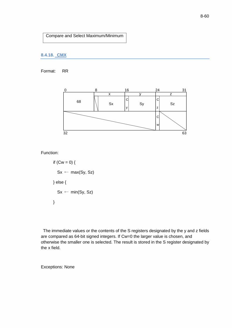
8-60
Compare and Select Maximum/Minimum
8.4.18. CMX
Format: RR
x
68 Sx Sy Sz
y
C
y
z
C
z
8 16 24 31
32 63
0
C
w
Function:
if (Cw = 0) {
Sx ← max(Sy, Sz)
} else {
Sx ← min(Sy, Sz)
}
The immediate values or the contents of the S registers designated by the y and z fields
are compared as 64-bit signed integers. If Cw=0 the larger value is chosen, and
otherwise the smaller one is selected. The result is stored in the S register designated by
the x field.
Exceptions: None
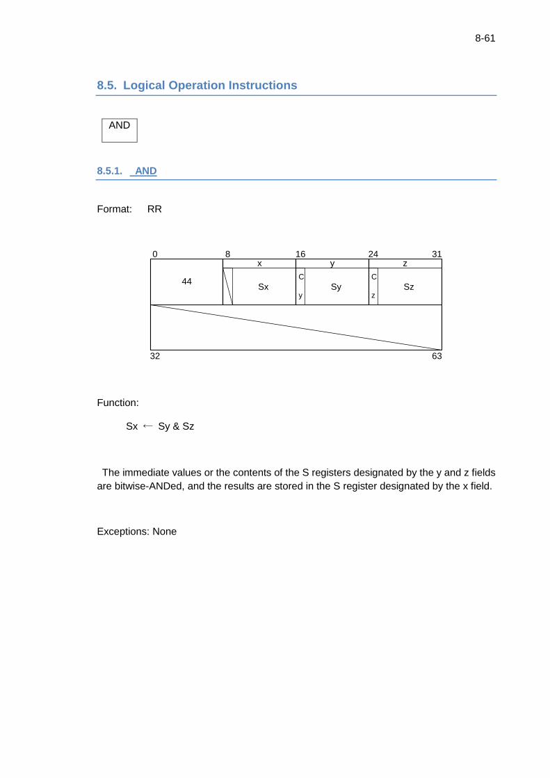
8-61
8.5. Logical Operation Instructions
AND
8.5.1. AND
Format: RR
x
44 Sx Sy Sz
y
C
y
z
C
z
8 16 24 31
32 63
0
Function:
Sx ← Sy & Sz
The immediate values or the contents of the S registers designated by the y and z fields
are bitwise-ANDed, and the results are stored in the S register designated by the x field.
Exceptions: None
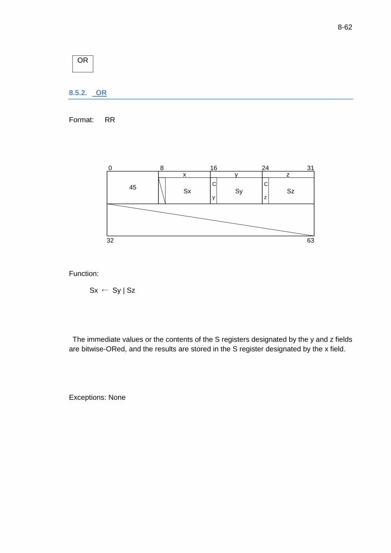
8-62
OR
8.5.2. OR
Format: RR
x
45 Sx Sy Sz
y
C
y
z
C
z
8 16 24 31
32 63
0
Function:
Sx ← Sy | Sz
The immediate values or the contents of the S registers designated by the y and z fields
are bitwise-ORed, and the results are stored in the S register designated by the x field.
Exceptions: None
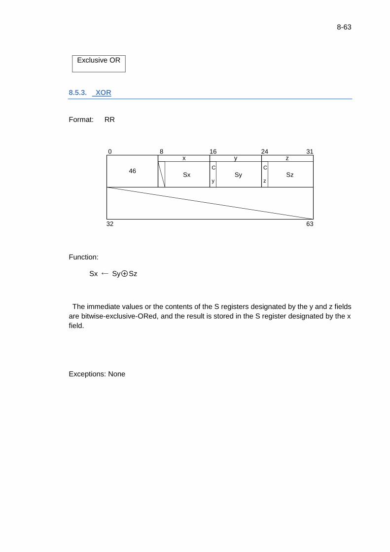
8-63
Exclusive OR
8.5.3. XOR
Format: RR
x
46 Sx Sy Sz
y
C
y
z
C
z
8 16 24 31
32 63
0
Function:
Sx ← Sy + Sz
The immediate values or the contents of the S registers designated by the y and z fields
are bitwise-exclusive-ORed, and the result is stored in the S register designated by the x
field.
Exceptions: None
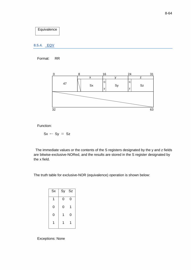
8-64
Equivalence
8.5.4. EQV
Format: RR
x
47 Sx Sy Sz
y
C
y
z
C
z
8 16 24 31
32 63
0
Function:
Sx ← Sy ≡ Sz
The immediate values or the contents of the S registers designated by the y and z fields
are bitwise-exclusive-NORed, and the results are stored in the S register designated by
the x field.
The truth table for exclusive-NOR (equivalence) operation is shown below:
Sx Sy Sz
1 0 0
0 0 1
0 1 0
1 1 1
Exceptions: None
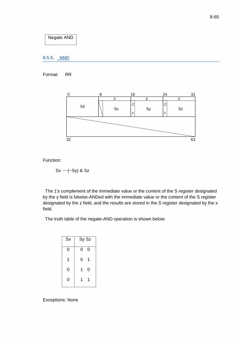
8-65
Negate AND
8.5.5. NND
Format: RR
x
54 Sx Sy Sz
y
C
y
z
C
z
8 16 24 31
32 63
0
Function:
Sx ←(~Sy) & Sz
The 1's complement of the immediate value or the content of the S register designated
by the y field is bitwise-ANDed with the immediate value or the content of the S register
designated by the z field, and the results are stored in the S register designated by the x
field.
The truth table of the negate-AND operation is shown below:
Sx Sy Sz
0 0 0
1 0 1
0 1 0
0 1 1
Exceptions: None
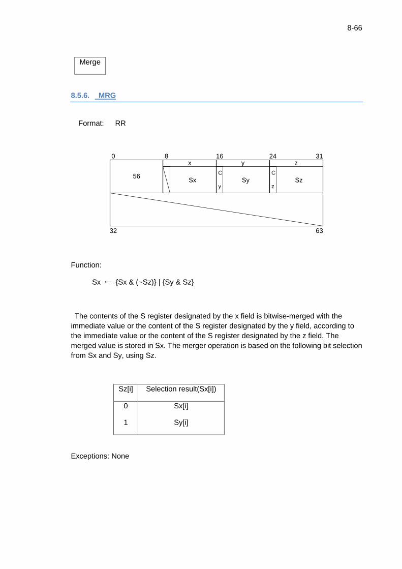
8-66
Merge
8.5.6. MRG
Format: RR
x
56 Sx Sy Sz
y
C
y
z
C
z
8 16 24 31
32 63
0
Function:
Sx ← {Sx & (~Sz)} | {Sy & Sz}
The contents of the S register designated by the x field is bitwise-merged with the
immediate value or the content of the S register designated by the y field, according to
the immediate value or the content of the S register designated by the z field. The
merged value is stored in Sx. The merger operation is based on the following bit selection
from Sx and Sy, using Sz.
Sz[i] Selection result(Sx[i])
0 Sx[i]
1 Sy[i]
Exceptions: None
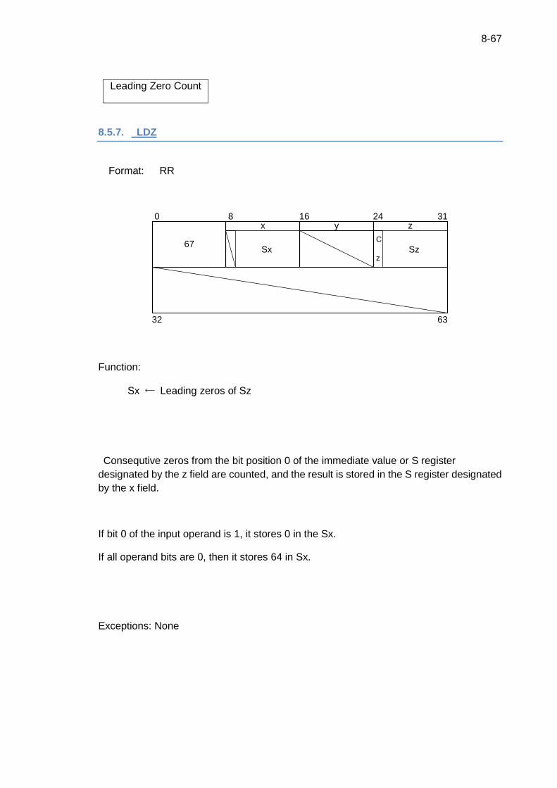
8-67
Leading Zero Count
8.5.7. LDZ
Format: RR
x
67 Sx Sz
y z
C
z
8 16 24 31
32 63
0
Function:
Sx ← Leading zeros of Sz
Consequtive zeros from the bit position 0 of the immediate value or S register
designated by the z field are counted, and the result is stored in the S register designated
by the x field.
If bit 0 of the input operand is 1, it stores 0 in the Sx.
If all operand bits are 0, then it stores 64 in Sx.
Exceptions: None
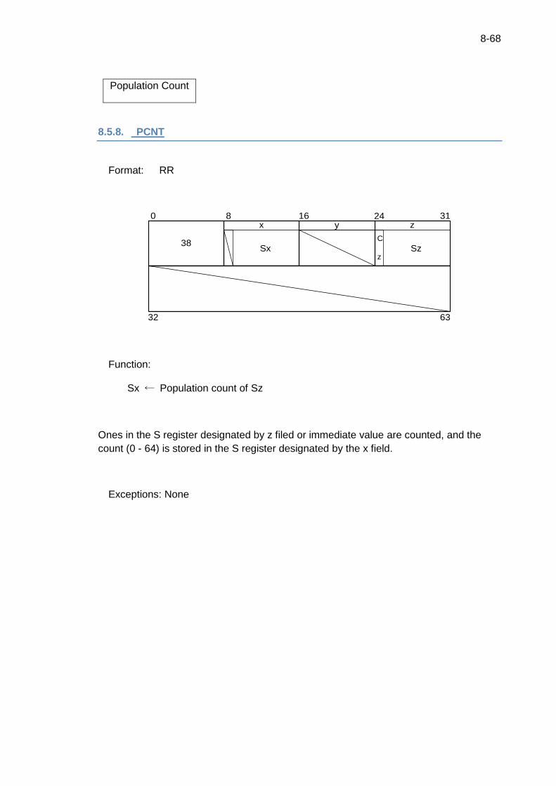
8-68
Population Count
8.5.8. PCNT
Format: RR
x
38 Sx Sz
y z
C
z
8 16 24 31
32 63
0
Function:
Sx ← Population count of Sz
Ones in the S register designated by z filed or immediate value are counted, and the
count (0 - 64) is stored in the S register designated by the x field.
Exceptions: None
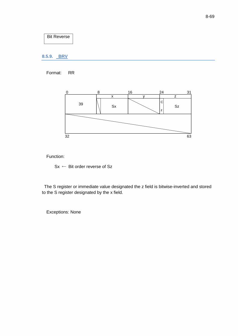
8-69
Bit Reverse
8.5.9. BRV
Format: RR
x
39 Sx Sz
y z
C
z
8 16 24 31
32 63
0
Function:
Sx ← Bit order reverse of Sz
The S register or immediate value designated the z field is bitwise-inverted and stored
to the S register designated by the x field.
Exceptions: None
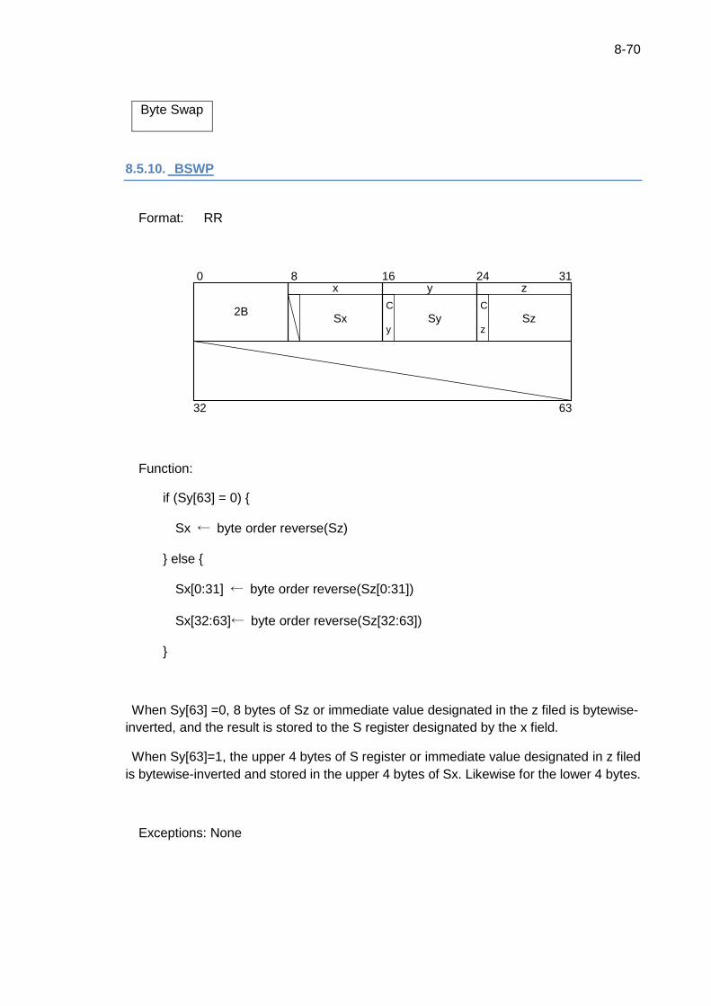
8-70
Byte Swap
8.5.10. BSWP
Format: RR
x
2B Sx Sy Sz
y
C
y
z
C
z
8 16 24 31
32 63
0
Function:
if (Sy[63] = 0) {
Sx ← byte order reverse(Sz)
} else {
Sx[0:31] ← byte order reverse(Sz[0:31])
Sx[32:63]← byte order reverse(Sz[32:63])
}
When Sy[63] =0, 8 bytes of Sz or immediate value designated in the z filed is bytewise-
inverted, and the result is stored to the S register designated by the x field.
When Sy[63]=1, the upper 4 bytes of S register or immediate value designated in z filed
is bytewise-inverted and stored in the upper 4 bytes of Sx. Likewise for the lower 4 bytes.
Exceptions: None
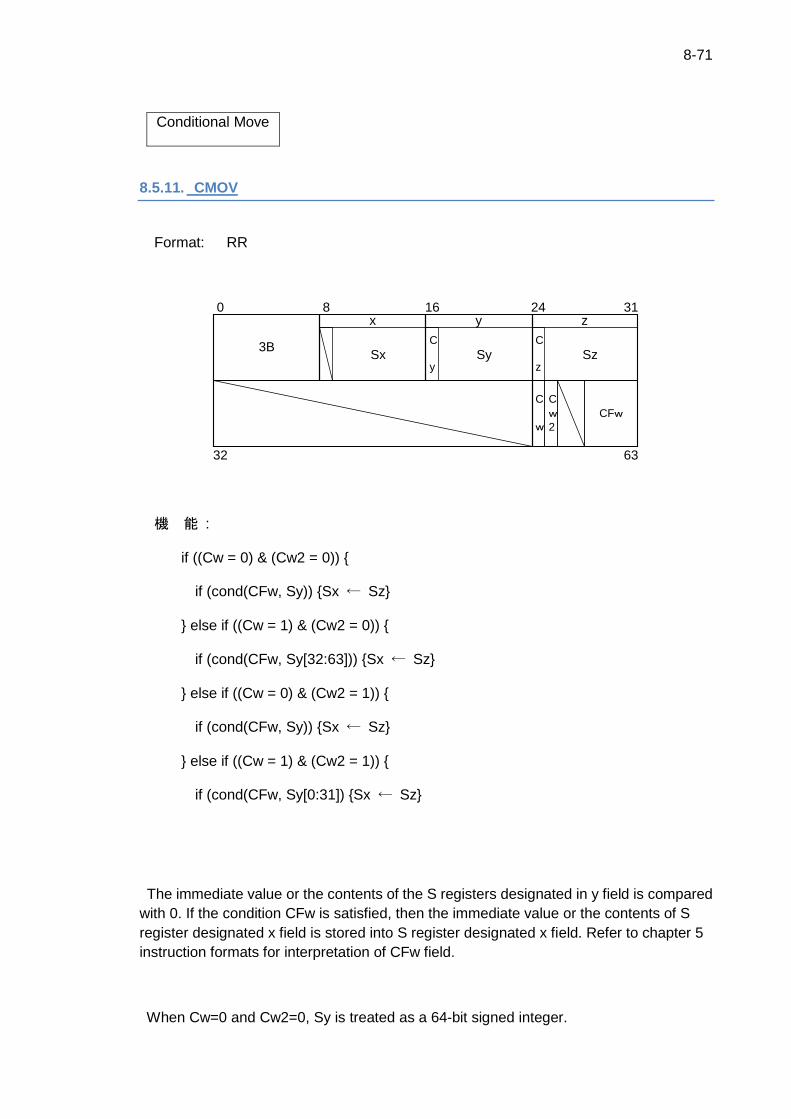
8-71
Conditional Move
8.5.11. CMOV
Format: RR
x
3B Sx Sy Sz
y
C
y
z
C
z
8 16 24 31
32 63
0
C
w
C
w2
CFw
機 能 :
if ((Cw = 0) & (Cw2 = 0)) {
if (cond(CFw, Sy)) {Sx ← Sz}
} else if ((Cw = 1) & (Cw2 = 0)) {
if (cond(CFw, Sy[32:63])) {Sx ← Sz}
} else if ((Cw = 0) & (Cw2 = 1)) {
if (cond(CFw, Sy)) {Sx ← Sz}
} else if ((Cw = 1) & (Cw2 = 1)) {
if (cond(CFw, Sy[0:31]) {Sx ← Sz}
The immediate value or the contents of the S registers designated in y field is compared
with 0. If the condition CFw is satisfied, then the immediate value or the contents of S
register designated x field is stored into S register designated x field. Refer to chapter 5
instruction formats for interpretation of CFw field.
When Cw=0 and Cw2=0, Sy is treated as a 64-bit signed integer.

8-72
When Cw=1, Cw2=0, Sy is treated as 32-bit signed integer.
When Cw=0, Cw2=1, Sy is treated as double precision floating point data.
When Cw=1, Cw2=1, Sy is treated as single precision floating point data.
If Cw2=1 and Sy’s exponent portion is all 0, Sy is regarded as a floating point 0.
Exceptions: None
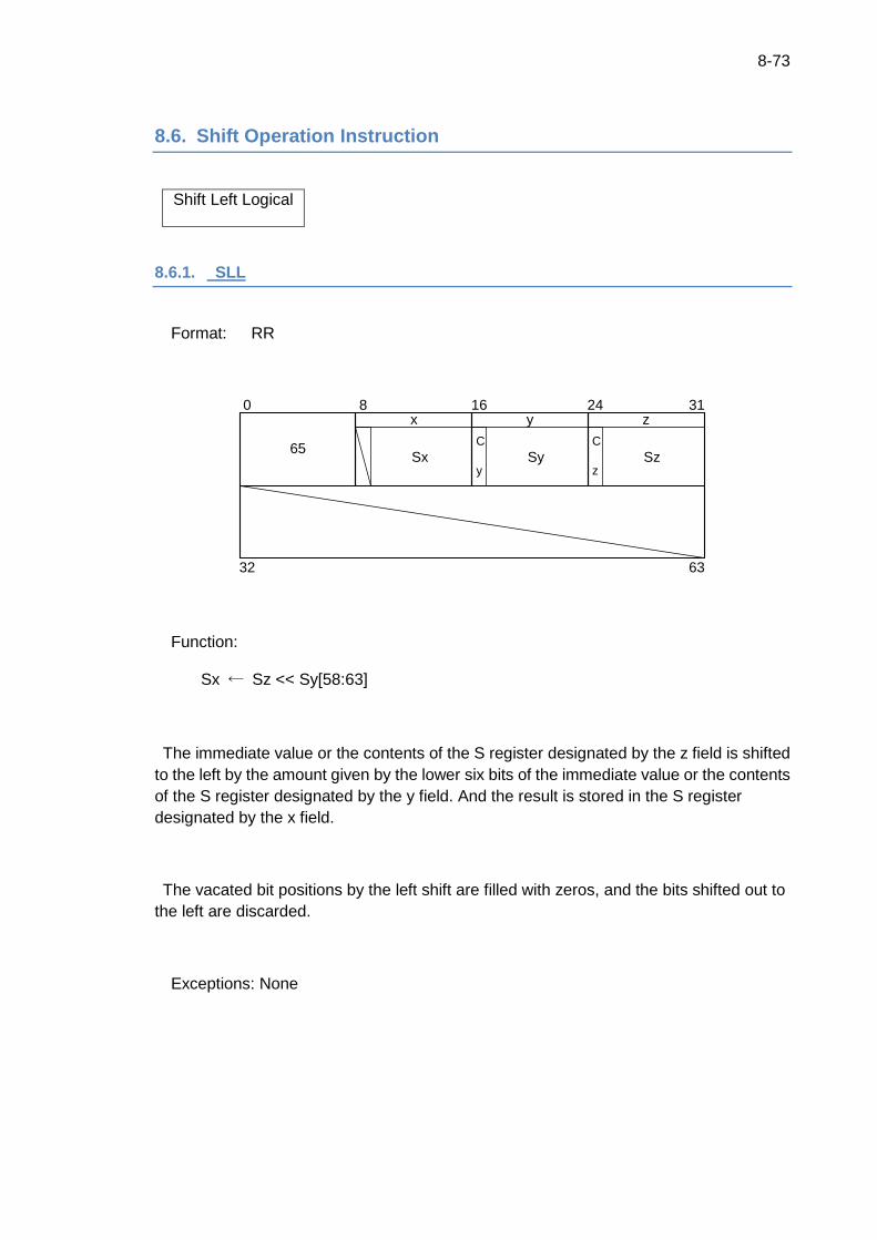
8-73
8.6. Shift Operation Instruction
Shift Left Logical
8.6.1. SLL
Format: RR
x
65 Sx Sy Sz
y
C
y
z
C
z
8 16 24 31
32 63
0
Function:
Sx ← Sz << Sy[58:63]
The immediate value or the contents of the S register designated by the z field is shifted
to the left by the amount given by the lower six bits of the immediate value or the contents
of the S register designated by the y field. And the result is stored in the S register
designated by the x field.
The vacated bit positions by the left shift are filled with zeros, and the bits shifted out to
the left are discarded.
Exceptions: None
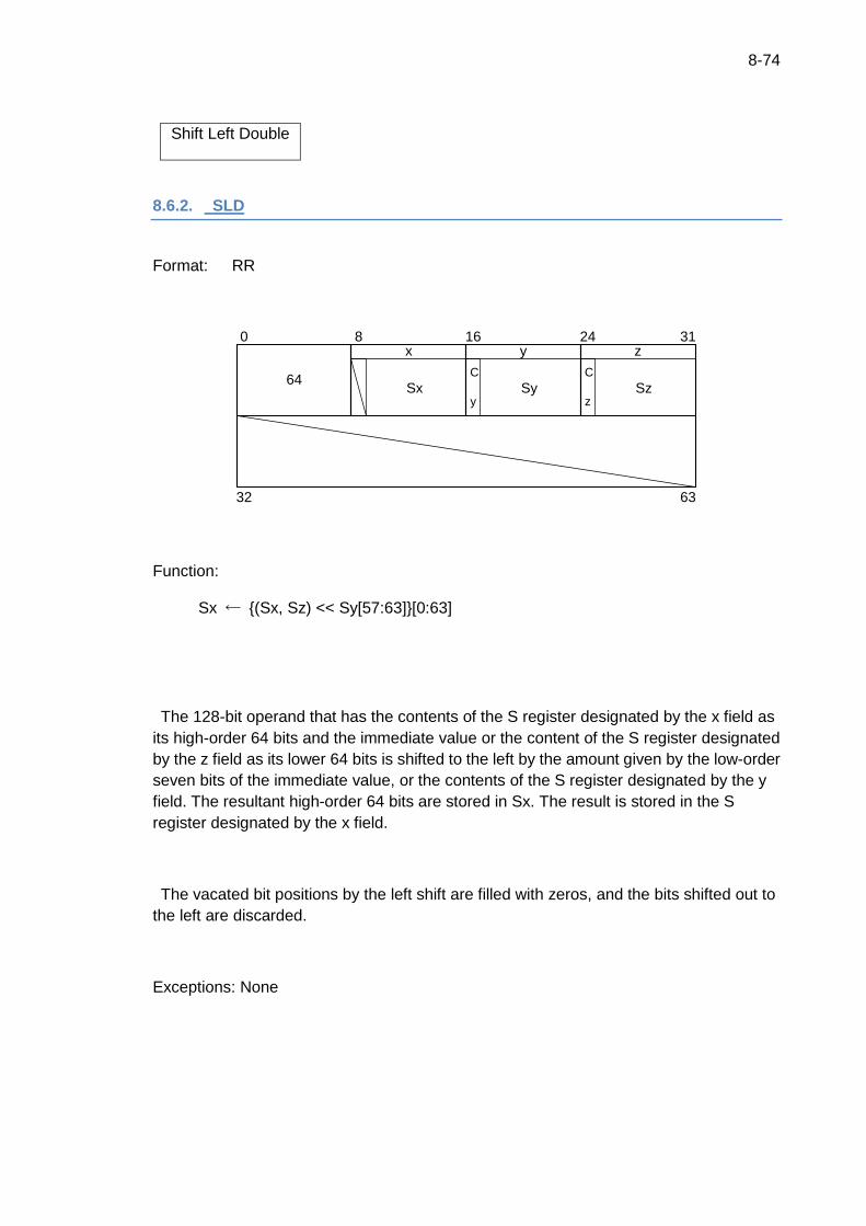
8-74
Shift Left Double
8.6.2. SLD
Format: RR
x
64 Sx Sy Sz
y
C
y
z
C
z
8 16 24 31
32 63
0
Function:
Sx ← {(Sx, Sz) << Sy[57:63]}[0:63]
The 128-bit operand that has the contents of the S register designated by the x field as
its high-order 64 bits and the immediate value or the content of the S register designated
by the z field as its lower 64 bits is shifted to the left by the amount given by the low-order
seven bits of the immediate value, or the contents of the S register designated by the y
field. The resultant high-order 64 bits are stored in Sx. The result is stored in the S
register designated by the x field.
The vacated bit positions by the left shift are filled with zeros, and the bits shifted out to
the left are discarded.
Exceptions: None
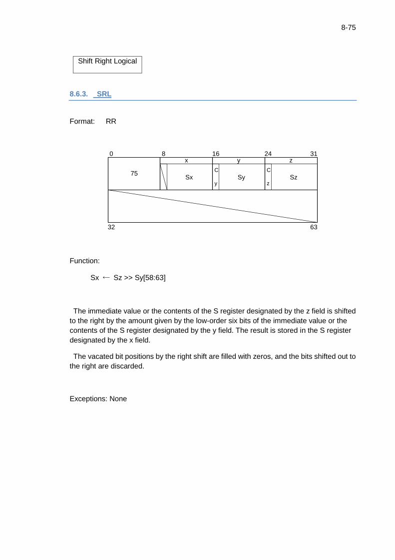
8-75
Shift Right Logical
8.6.3. SRL
Format: RR
x
75 Sx Sy Sz
y
C
y
z
C
z
8 16 24 31
32 63
0
Function:
Sx ← Sz >> Sy[58:63]
The immediate value or the contents of the S register designated by the z field is shifted
to the right by the amount given by the low-order six bits of the immediate value or the
contents of the S register designated by the y field. The result is stored in the S register
designated by the x field.
The vacated bit positions by the right shift are filled with zeros, and the bits shifted out to
the right are discarded.
Exceptions: None
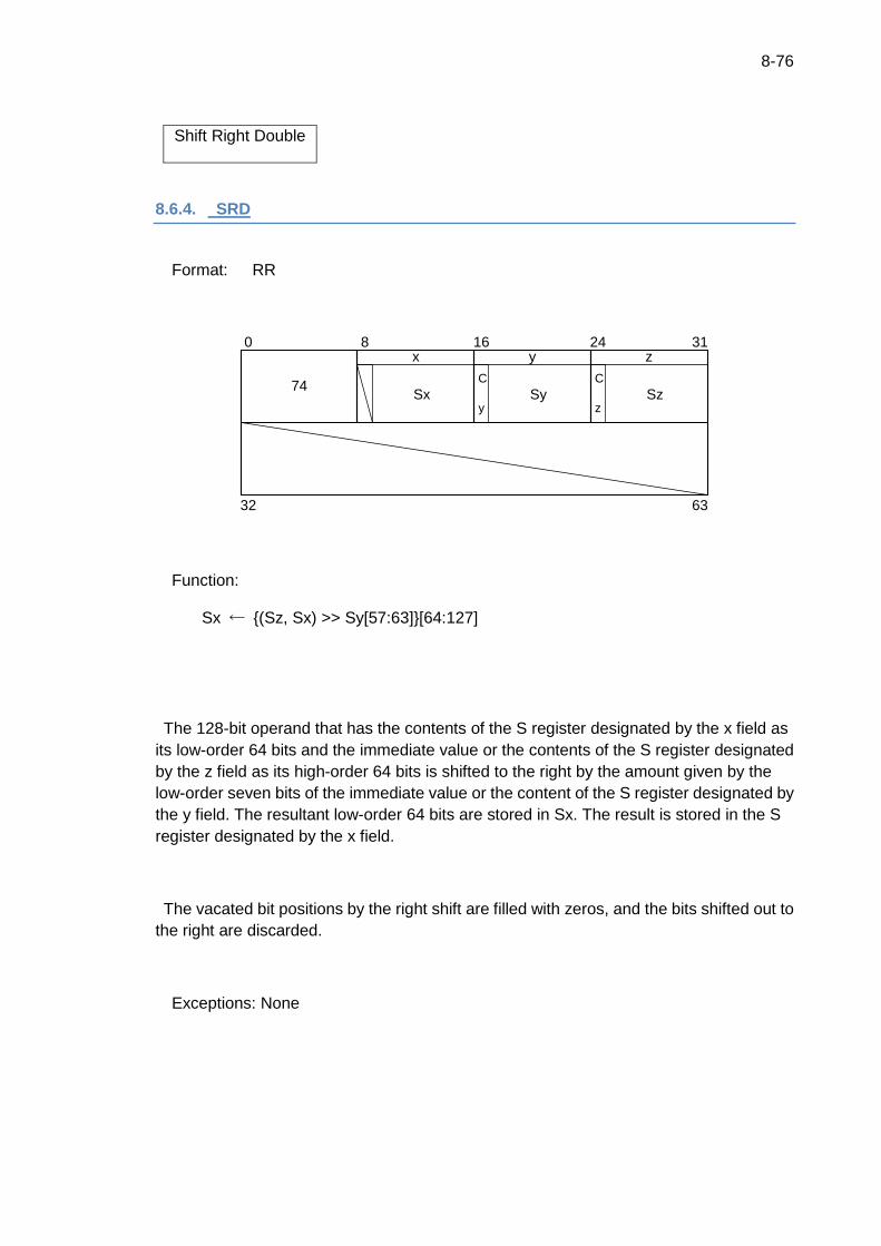
8-76
Shift Right Double
8.6.4. SRD
Format: RR
x
74 Sx Sy Sz
y
C
y
z
C
z
8 16 24 31
32 63
0
Function:
Sx ← {(Sz, Sx) >> Sy[57:63]}[64:127]
The 128-bit operand that has the contents of the S register designated by the x field as
its low-order 64 bits and the immediate value or the contents of the S register designated
by the z field as its high-order 64 bits is shifted to the right by the amount given by the
low-order seven bits of the immediate value or the content of the S register designated by
the y field. The resultant low-order 64 bits are stored in Sx. The result is stored in the S
register designated by the x field.
The vacated bit positions by the right shift are filled with zeros, and the bits shifted out to
the right are discarded.
Exceptions: None
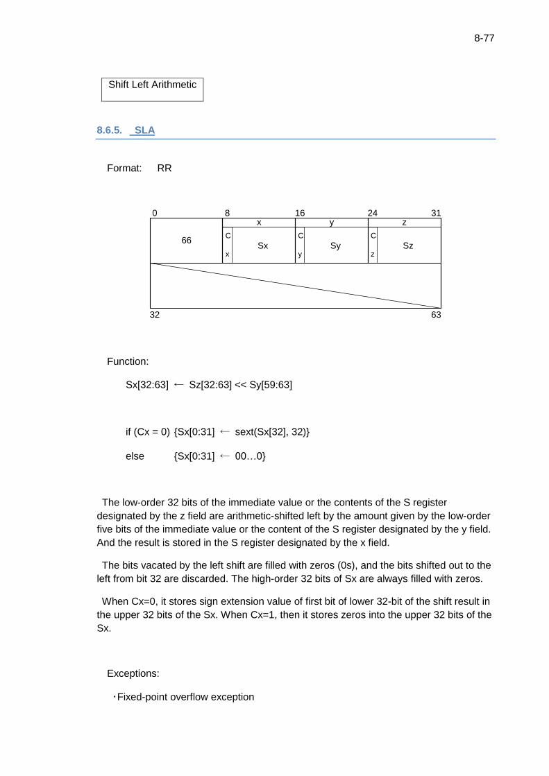
8-77
Shift Left Arithmetic
8.6.5. SLA
Format: RR
x
66 Sx Sy Sz
y
C
y
z
C
z
8 16 24 31
32 63
0
C
x
Function:
Sx[32:63] ← Sz[32:63] << Sy[59:63]
if (Cx = 0) {Sx[0:31] ← sext(Sx[32], 32)}
else {Sx[0:31] ← 00…0}
The low-order 32 bits of the immediate value or the contents of the S register
designated by the z field are arithmetic-shifted left by the amount given by the low-order
five bits of the immediate value or the content of the S register designated by the y field.
And the result is stored in the S register designated by the x field.
The bits vacated by the left shift are filled with zeros (0s), and the bits shifted out to the
left from bit 32 are discarded. The high-order 32 bits of Sx are always filled with zeros.
When Cx=0, it stores sign extension value of first bit of lower 32-bit of the shift result in
the upper 32 bits of the Sx. When Cx=1, then it stores zeros into the upper 32 bits of the
Sx.
Exceptions:
・Fixed-point overflow exception
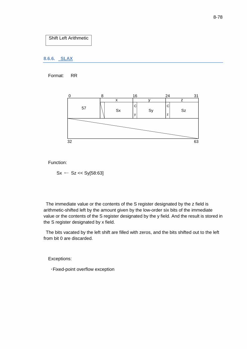
8-78
Shift Left Arithmetic
8.6.6. SLAX
Format: RR
x
57 Sx Sy Sz
y
C
y
z
C
z
8 16 24 31
32 63
0
Function:
Sx ← Sz << Sy[58:63]
The immediate value or the contents of the S register designated by the z field is
arithmetic-shifted left by the amount given by the low-order six bits of the immediate
value or the contents of the S register designated by the y field. And the result is stored in
the S register designated by x field.
The bits vacated by the left shift are filled with zeros, and the bits shifted out to the left
from bit 0 are discarded.
Exceptions:
・Fixed-point overflow exception
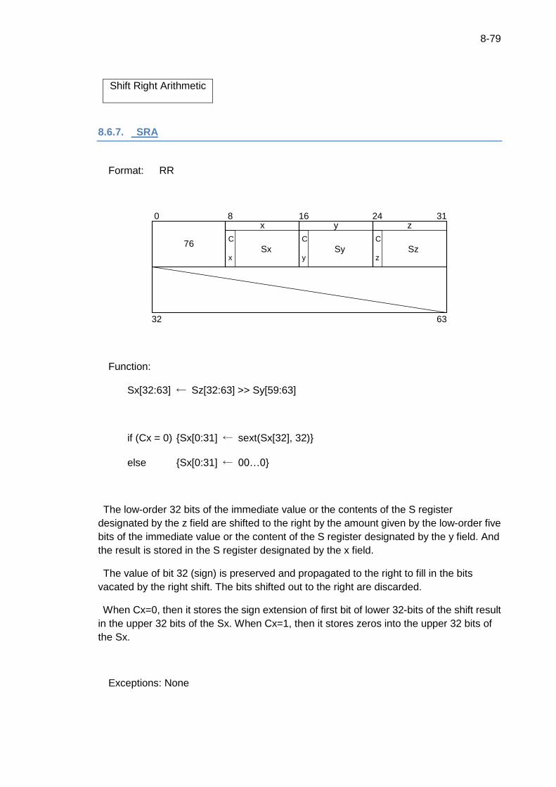
8-79
Shift Right Arithmetic
8.6.7. SRA
Format: RR
x
76 Sx Sy Sz
y
C
y
z
C
z
8 16 24 31
32 63
0
C
x
Function:
Sx[32:63] ← Sz[32:63] >> Sy[59:63]
if (Cx = 0) {Sx[0:31] ← sext(Sx[32], 32)}
else {Sx[0:31] ← 00…0}
The low-order 32 bits of the immediate value or the contents of the S register
designated by the z field are shifted to the right by the amount given by the low-order five
bits of the immediate value or the content of the S register designated by the y field. And
the result is stored in the S register designated by the x field.
The value of bit 32 (sign) is preserved and propagated to the right to fill in the bits
vacated by the right shift. The bits shifted out to the right are discarded.
When Cx=0, then it stores the sign extension of first bit of lower 32-bits of the shift result
in the upper 32 bits of the Sx. When Cx=1, then it stores zeros into the upper 32 bits of
the Sx.
Exceptions: None
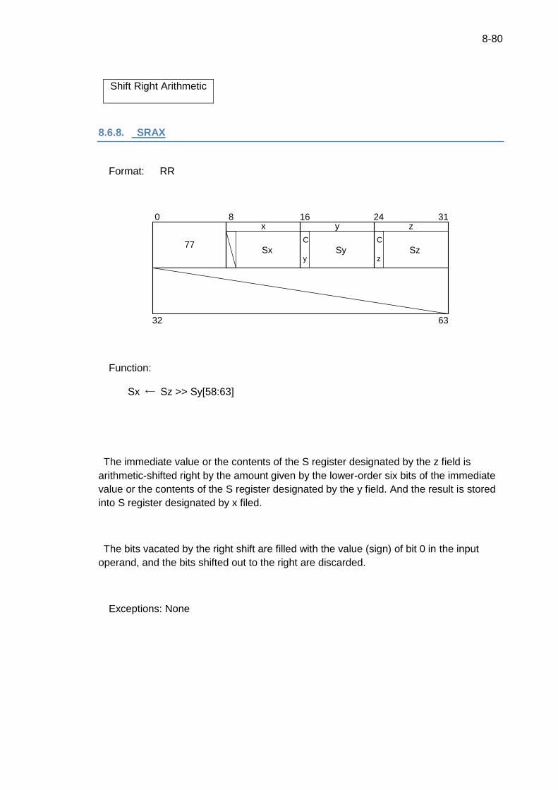
8-80
Shift Right Arithmetic
8.6.8. SRAX
Format: RR
x
77 Sx Sy Sz
y
C
y
z
C
z
8 16 24 31
32 63
0
Function:
Sx ← Sz >> Sy[58:63]
The immediate value or the contents of the S register designated by the z field is
arithmetic-shifted right by the amount given by the lower-order six bits of the immediate
value or the contents of the S register designated by the y field. And the result is stored
into S register designated by x filed.
The bits vacated by the right shift are filled with the value (sign) of bit 0 in the input
operand, and the bits shifted out to the right are discarded.
Exceptions: None
8-81
8.7. Floating-Point Arithmetic Instructions
Floating Add
8.7.1. FAD
Format RR
x
4C Sx Sy Sz
y
C
y
z
C
z
8 16 24 31
32 63
0
C
x
Function:
if (Cx = 0) {
Sx ← Sy + Sz
} else {
Sx[0:31] ← Sy[0:31] + Sz[0:31]
Sx[32:63] ← 00…0
}
The contents of the S registers designated by the y and z fields of the instruction or the
immediate values are added as floating-point data. The result is normalized, and stored
in the S register designated by the x field.
When Cx=0, the contents of the S registers designated in each field of the instruction or
the immediate values are regarded as double-precision floating point data. When Cx=1,
these data are regarded as single-precision floating point data.
8-82
Exceptions:
・Floating-point overflow exception
・Floating-point underflow exception
・Invalid operation exception
・Inexact exception
Notes:
・When Cy=0, Sy field indicates an immediate value of signed integer (-63 to 64).
・When Cz=0, Sz field indicates an immediate value with a bit pattern composed of
continuous 0s and 1s. See also 5.4.3 for the detail.
8-83
Floating Subtract
8.7.2. FSB
Format : RR
C
x
x
5C Sx Sy Sz
y
C
y
z
C
z
8 16 24 31
32 63
0
Function:
if (Cx = 0) {
Sx ← Sy - Sz
} else {
Sx[0:31] ← Sy[0:31] - Sz[0:31]
Sx[32:63] ← 00…0
}
The contents of the S register designated by the z field of the instruction or the
immediate value is subtracted as floating-point data from the contents of the S register
designated by the y field or the immediate value. The result is normalized, then stored in
the S register designated by the x field.
When Cx=0, the contents of the S registers designated in each field of the instruction or
the immediate values are regarded as double-precision floating point data. When Cx=1,
these data are regarded as single-precision floating point data.
8-84
Exceptions:
・Floating-point overflow exception
・Floating-point underflow exception
・Invalid operation exception
・Inexact exception
Notes:
・See Notes on the FAD instruction.
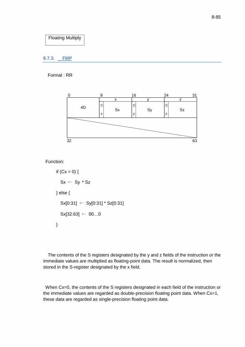
8-85
Floating Multiply
8.7.3. FMP
Format : RR
x
4D Sx Sy Sz
y
C
y
z
C
z
8 16 24 31
32 63
0
C
x
Function:
if (Cx = 0) {
Sx ← Sy * Sz
} else {
Sx[0:31] ← Sy[0:31] * Sz[0:31]
Sx[32:63] ← 00…0
}
The contents of the S registers designated by the y and z fields of the instruction or the
immediate values are multiplied as floating-point data. The result is normalized, then
stored in the S-register designated by the x field.
When Cx=0, the contents of the S registers designated in each field of the instruction or
the immediate values are regarded as double-precision floating point data. When Cx=1,
these data are regarded as single-precision floating point data.
8-86
Exceptions:
・Floating-point overflow exception
・Floating-point underflow exception
・Invalid operation exception
・Inexact exception
Notes:
・See Notes on the FAD instruction.
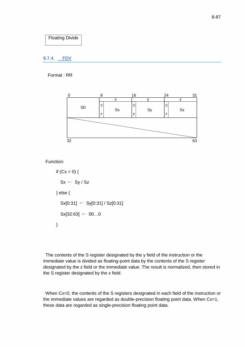
8-87
Floating Divide
8.7.4. FDV
Format : RR
x
5D Sx Sy Sz
y
C
y
z
C
z
8 16 24 31
32 63
0
C
x
Function:
if (Cx = 0) {
Sx ← Sy / Sz
} else {
Sx[0:31] ← Sy[0:31] / Sz[0:31]
Sx[32:63] ← 00…0
}
The contents of the S register designated by the y field of the instruction or the
immediate value is divided as floating-point data by the contents of the S register
designated by the z field or the immediate value. The result is normalized, then stored in
the S register designated by the x field.
When Cx=0, the contents of the S registers designated in each field of the instruction or
the immediate values are regarded as double-precision floating point data. When Cx=1,
these data are regarded as single-precision floating point data.
8-88
Exceptions:
・Floating-point overflow exception
・Floating-point underflow exception
・Invalid operation exception
・Inexact exception
・Divide exception
Notes:
・See Notes on the FAD instruction.
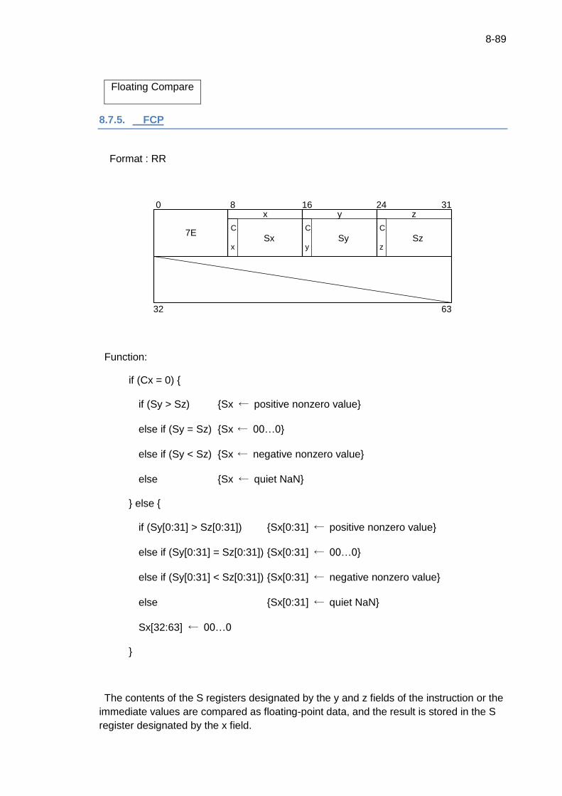
8-89
Floating Compare
8.7.5. FCP
Format : RR
x
7E Sx Sy Sz
y
C
y
z
C
z
8 16 24 31
32 63
0
C
x
Function:
if (Cx = 0) {
if (Sy > Sz) {Sx ← positive nonzero value}
else if (Sy = Sz) {Sx ← 00…0}
else if (Sy < Sz) {Sx ← negative nonzero value}
else {Sx ← quiet NaN}
} else {
if (Sy[0:31] > Sz[0:31]) {Sx[0:31] ← positive nonzero value}
else if (Sy[0:31] = Sz[0:31]) {Sx[0:31] ← 00…0}
else if (Sy[0:31] < Sz[0:31]) {Sx[0:31] ← negative nonzero value}
else {Sx[0:31] ← quiet NaN}
Sx[32:63] ← 00…0
}
The contents of the S registers designated by the y and z fields of the instruction or the
immediate values are compared as floating-point data, and the result is stored in the S
register designated by the x field.
8-90
When Sy>Sz, zero is stored into the sign field of Sx and a value greater than or equal
to Emin, but less than or equal to Emax is stored into the exponent field E (the mantissa
F is undefined), or Emax + 1 is stored into the exponent field E and 0 is stored into the
mantissa F.
If Sy=Sz, zero is stored into the bit positions corresponding to the exponent field of Sx.
The values of the bit positions other than the exponent field are undefined.
If Sy<Sz, 1 is stored into the sign field of Sx and a value greater than or equal to Emin,
but less than or equal to Emax is stored into the exponent field E (the mantissa F is
undefined), or Emax + 1 is stored into the exponent field E and 0 is stored into the
mantissa F.
In all cases, floating-point overflow exception, floating-point underflow exception, or
inexact exception won’t occur irrespective of the value of the exception mask.
When Cx=0, the contents of the S registers designated in each field of the instruction or
the immediate values are regarded as double-precision floating point data. When Cx=1,
these data are regarded as single-precision floating point data.
Exceptions:
・Invalid operation exception
Notes:
・See Notes on the FAD instruction.
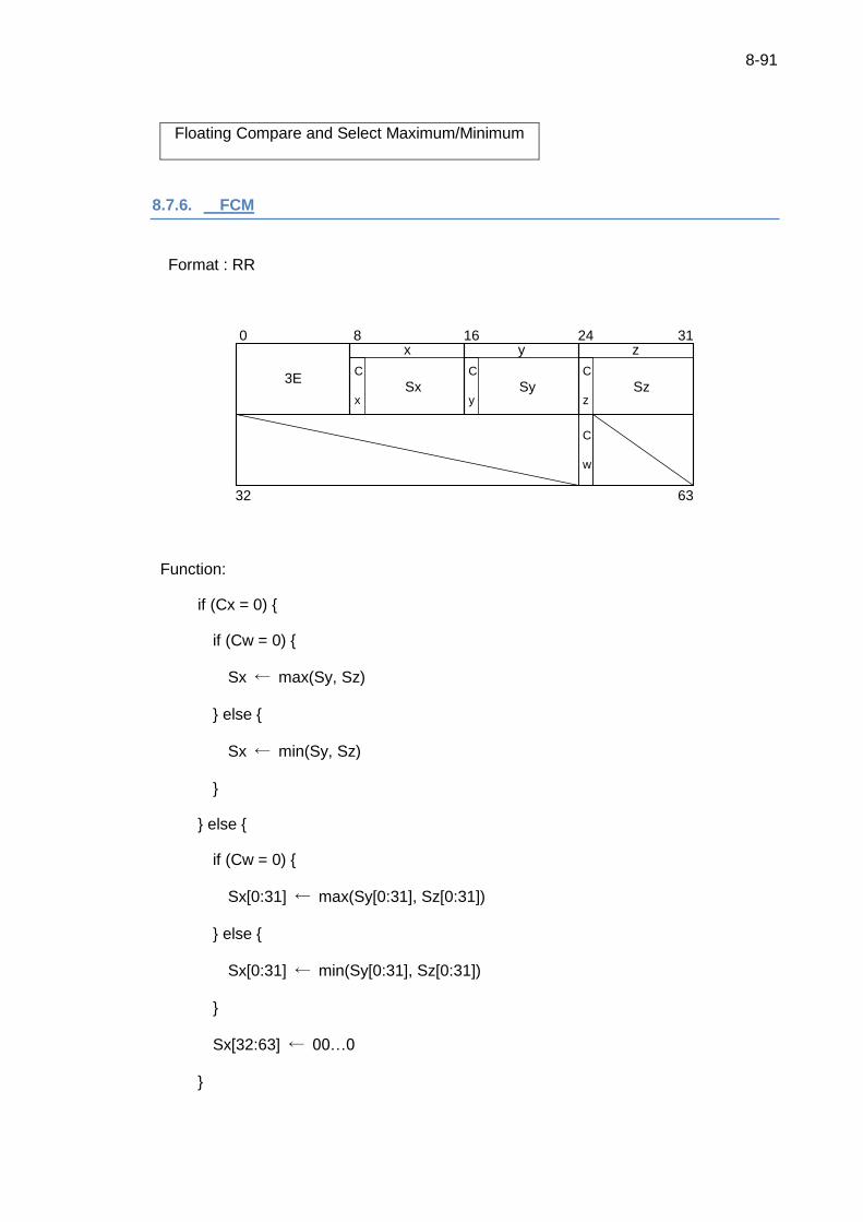
8-91
Floating Compare and Select Maximum/Minimum
8.7.6. FCM
Format : RR
x
3E Sx Sy Sz
y
C
y
z
C
z
8 16 24 31
32 63
0
C
x
C
w
Function:
if (Cx = 0) {
if (Cw = 0) {
Sx ← max(Sy, Sz)
} else {
Sx ← min(Sy, Sz)
}
} else {
if (Cw = 0) {
Sx[0:31] ← max(Sy[0:31], Sz[0:31])
} else {
Sx[0:31] ← min(Sy[0:31], Sz[0:31])
}
Sx[32:63] ← 00…0
}
8-92
The contents of the S register designated by the y and z fields of the instruction or the
immediate values are compared as floating-point data.
When Cw=0, the contents of big one is stored in the S register designated by the x
field.
When Cw=1, the contents of small one is stored in the S register designated by the x
field.
+0 and -0 are regarded as the same value. If both y and z operands are zero, the result
is zero with z operand’s sign bit.
When Cx=0, the contents of the S register designated by the x, y and z fields of the
instruction or the immediate values are regarded as conforming to the IEEE
double-precision floating-point data format.
When Cx=1, the contents of the S register designated by the x, y and z fields of the
instruction or the immediate values are regarded as conforming to the IEEE
single-precision floating-point data format.
Exceptions:
・Invalid operation exception
Notes:
・See Notes on the FAD instruction.
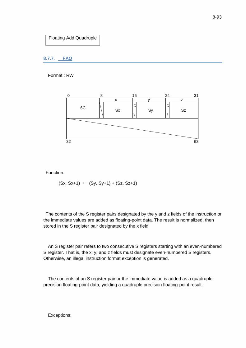
8-93
Floating Add Quadruple
8.7.7. FAQ
Format : RW
x
6C Sx Sy Sz
y
C
y
z
C
z
8 16 24 31
32 63
0
Function:
(Sx, Sx+1) ← (Sy, Sy+1) + (Sz, Sz+1)
The contents of the S register pairs designated by the y and z fields of the instruction or
the immediate values are added as floating-point data. The result is normalized, then
stored in the S register pair designated by the x field.
An S register pair refers to two consecutive S registers starting with an even-numbered
S register. That is, the x, y, and z fields must designate even-numbered S registers.
Otherwise, an illegal instruction format exception is generated.
The contents of an S register pair or the immediate value is added as a quadruple
precision floating-point data, yielding a quadruple precision floating-point result.
Exceptions:
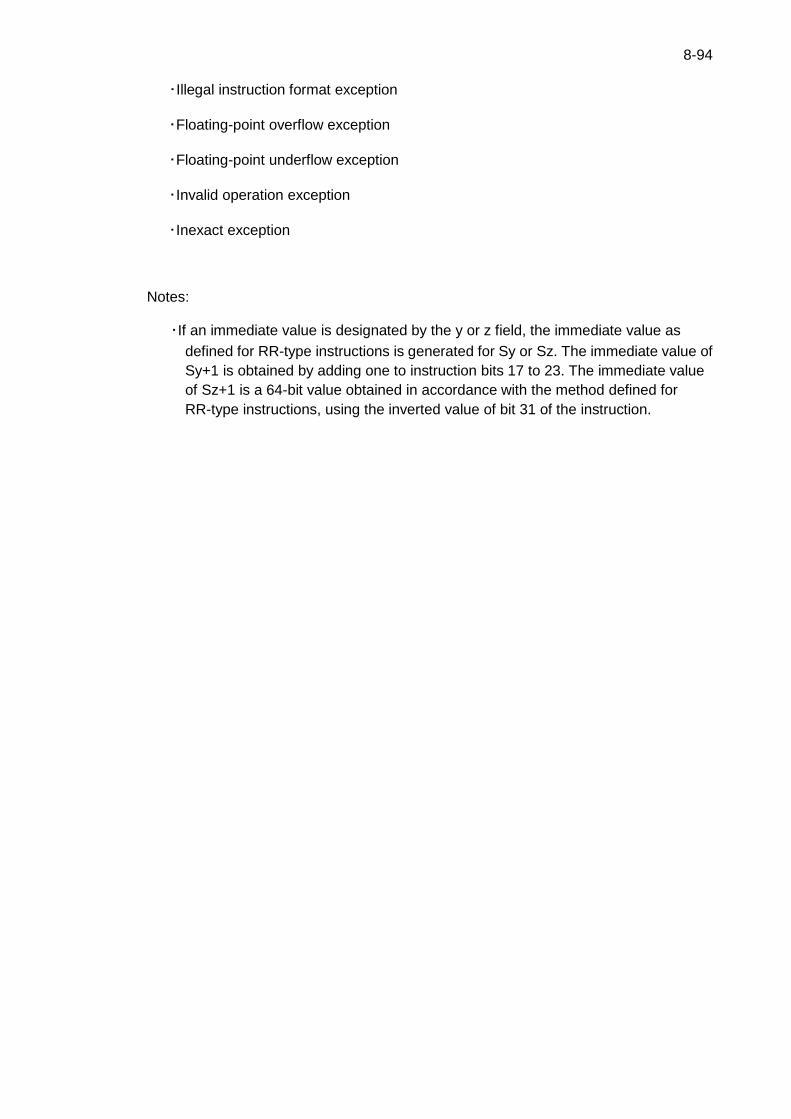
8-94
・Illegal instruction format exception
・Floating-point overflow exception
・Floating-point underflow exception
・Invalid operation exception
・Inexact exception
Notes:
・If an immediate value is designated by the y or z field, the immediate value as
defined for RR-type instructions is generated for Sy or Sz. The immediate value of
Sy+1 is obtained by adding one to instruction bits 17 to 23. The immediate value
of Sz+1 is a 64-bit value obtained in accordance with the method defined for
RR-type instructions, using the inverted value of bit 31 of the instruction.
8-95
Floating Subtract Quadruple
8.7.8. FSQ
Format : RW
x
7C Sx Sy Sz
y
C
y
z
C
z
8 16 24 31
32 63
0
Function:
(Sx, Sx+1) ← (Sy, Sy+1) - (Sz, Sz+1)
The contents of the S register pair designated by the z field of the instruction or the
immediate value is subtracted as floating-point data from the contents of the S register
pair designated by the y field or the immediate value. The result is normalized, then
stored in the S register pair designated by the x field.
An S register pair refers to two consecutive S registers starting with an even-numbered
S register. That is, the x, y, and z fields must designate even-numbered S registers.
Otherwise, an illegal instruction format exception is generated.
The contents of an S register pair or the immediate value is used in subtraction as a
quadruple precision floating-point data, providing a quadruple precision floating-point
result.
Exceptions:
・Illegal instruction format exception

8-96
・Floating-point overflow exception
・Floating-point underflow exception
・Invalid operation exception
・Inexact exception
Notes:
・See Notes on the FAQ instruction
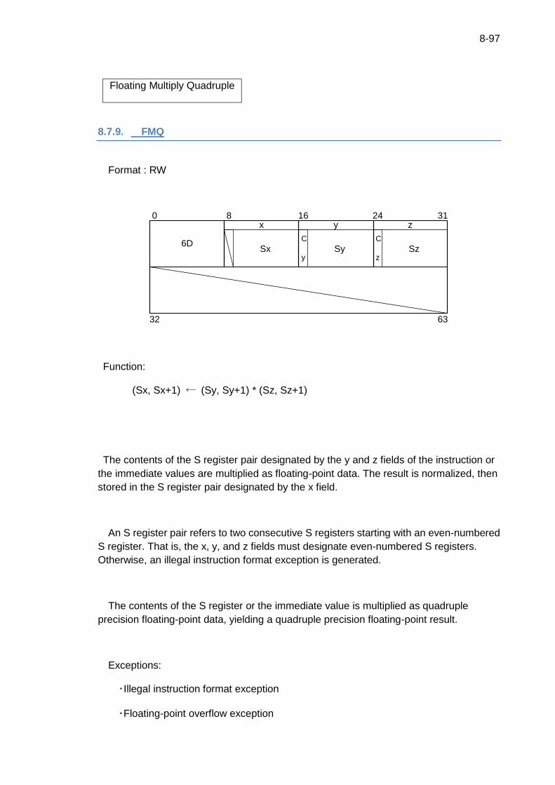
8-97
Floating Multiply Quadruple
8.7.9. FMQ
Format : RW
x
6D Sx Sy Sz
y
C
y
z
C
z
8 16 24 31
32 63
0
Function:
(Sx, Sx+1) ← (Sy, Sy+1) * (Sz, Sz+1)
The contents of the S register pair designated by the y and z fields of the instruction or
the immediate values are multiplied as floating-point data. The result is normalized, then
stored in the S register pair designated by the x field.
An S register pair refers to two consecutive S registers starting with an even-numbered
S register. That is, the x, y, and z fields must designate even-numbered S registers.
Otherwise, an illegal instruction format exception is generated.
The contents of the S register or the immediate value is multiplied as quadruple
precision floating-point data, yielding a quadruple precision floating-point result.
Exceptions:
・Illegal instruction format exception
・Floating-point overflow exception

8-98
・Floating-point underflow exception
・Invalid operation exception
・Inexact exception
Notes:
・See Notes on the FAQ instruction
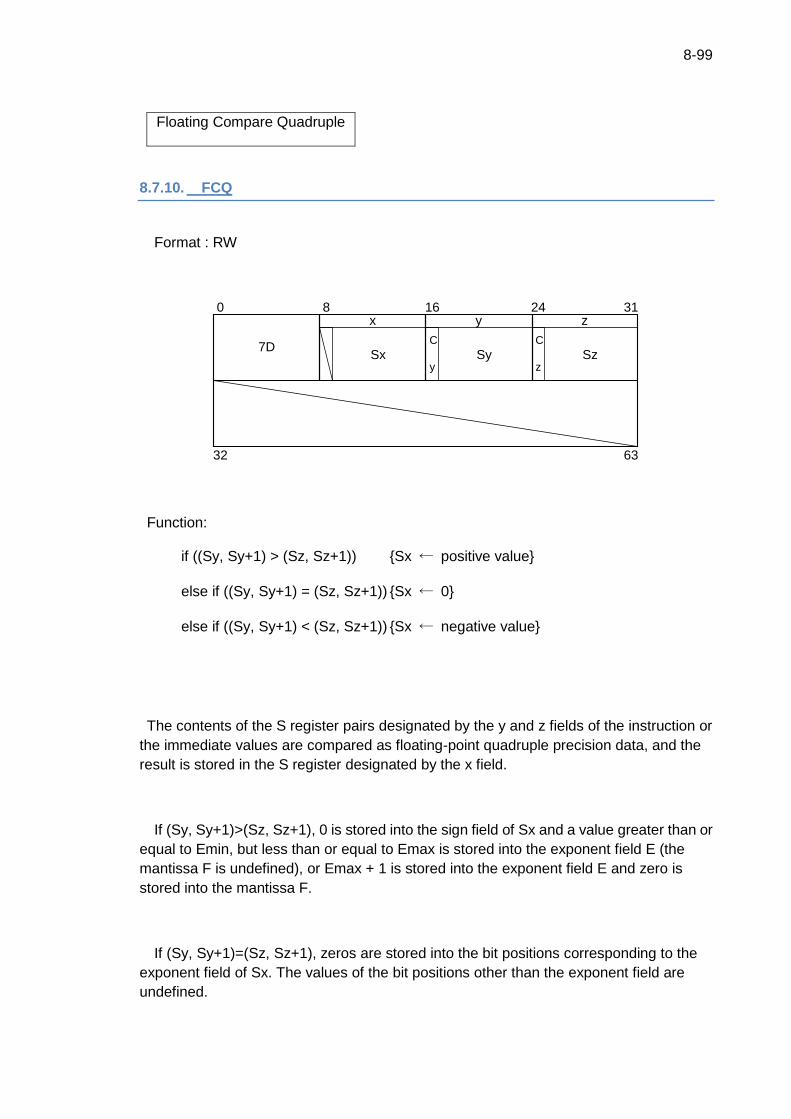
8-99
Floating Compare Quadruple
8.7.10. FCQ
Format : RW
x
7D Sx Sy Sz
y
C
y
z
C
z
8 16 24 31
32 63
0
Function:
if ((Sy, Sy+1) > (Sz, Sz+1)) {Sx ← positive value}
else if ((Sy, Sy+1) = (Sz, Sz+1)) {Sx ← 0}
else if ((Sy, Sy+1) < (Sz, Sz+1)) {Sx ← negative value}
The contents of the S register pairs designated by the y and z fields of the instruction or
the immediate values are compared as floating-point quadruple precision data, and the
result is stored in the S register designated by the x field.
If (Sy, Sy+1)>(Sz, Sz+1), 0 is stored into the sign field of Sx and a value greater than or
equal to Emin, but less than or equal to Emax is stored into the exponent field E (the
mantissa F is undefined), or Emax + 1 is stored into the exponent field E and zero is
stored into the mantissa F.
If (Sy, Sy+1)=(Sz, Sz+1), zeros are stored into the bit positions corresponding to the
exponent field of Sx. The values of the bit positions other than the exponent field are
undefined.
8-100
If (Sy, Sy+1)<(Sz, Sz+1), 1 is stored into the sign field of Sx and a value greater than or
equal to Emin, but less than or equal to Emax is stored into the exponent field E (the
mantissa F is undefined), or Emax + 1 is stored into the exponent field E and zero is
stored into the mantissa F.
In all cases, no floating-point overflow exception, floating-point underflow exception, or
inexact exception occurs irrespective of the value of the exception mask.
An S register pair refers to two consecutive S registers starting with an even-numbered
S register. The x field may designate any S registers from S0 to S63. The y and z fields
must designate even-numbered S registers. Otherwise, an illegal instruction format
exception occurs.
Exceptions:
・Illegal instruction format exception
・Invalid operation exception
Notes:
・See Notes on the FAQ instruction
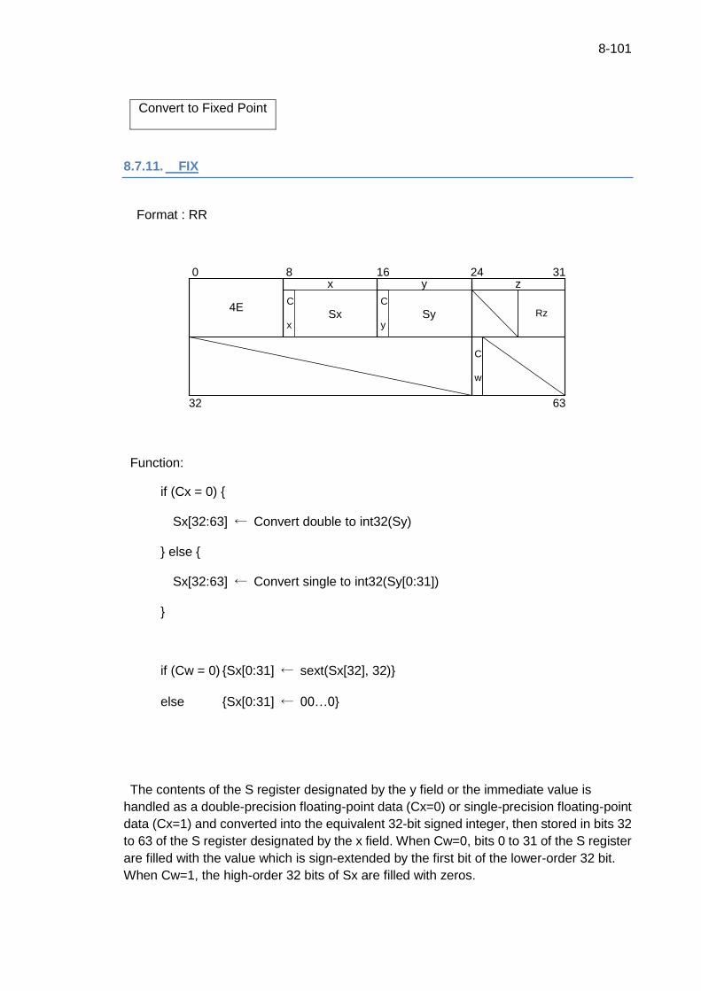
8-101
Convert to Fixed Point
8.7.11. FIX
Format : RR
x
4E Sx Sy
y
C
y
z8 16 24 31
32 63
0
C
x
C
w
Rz
Function:
if (Cx = 0) {
Sx[32:63] ← Convert double to int32(Sy)
} else {
Sx[32:63] ← Convert single to int32(Sy[0:31])
}
if (Cw = 0) {Sx[0:31] ← sext(Sx[32], 32)}
else {Sx[0:31] ← 00…0}
The contents of the S register designated by the y field or the immediate value is
handled as a double-precision floating-point data (Cx=0) or single-precision floating-point
data (Cx=1) and converted into the equivalent 32-bit signed integer, then stored in bits 32
to 63 of the S register designated by the x field. When Cw=0, bits 0 to 31 of the S register
are filled with the value which is sign-extended by the first bit of the lower-order 32 bit.
When Cw=1, the high-order 32 bits of Sx are filled with zeros.
8-102
The result is a 32-bit signed integer which is rounded according to the round mode
specified by the z field. When Rz =RFU, the conversion result is undefined.
0000:Round with designation of IRM ( bit 50-51 of PSW )
1000:Round toward Zero
1001:Round toward Plus infinity
1010:Round toward Minus infinity
1011:Round to Nearest (ties to even)
1100:Round to Nearest (ties to away)
other:RFU
When the conversion result exceeds the expression range of the 32bit signed integer,
an invalid operation exception occurs. It depends on state of invalid operation exception
mask whether an invalid operation exception interrupt occurs. If an invalid operation
exception occurs, the value of the register used for storing results will be undefined.
Exceptions:
・Invalid operation exception
・Inexact exception
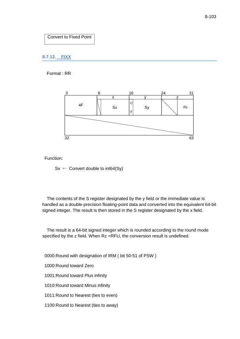
8-103
Convert to Fixed Point
8.7.12. FIXX
Format : RR
x
4F Sx Sy
y
C
y
z8 16 24 31
32 63
0
Rz
Function:
Sx ← Convert double to int64(Sy)
The contents of the S register designated by the y field or the immediate value is
handled as a double-precision floating-point data and converted into the equivalent 64-bit
signed integer. The result is then stored in the S register designated by the x field.
The result is a 64-bit signed integer which is rounded according to the round mode
specified by the z field. When Rz =RFU, the conversion result is undefined.
0000:Round with designation of IRM ( bit 50-51 of PSW )
1000:Round toward Zero
1001:Round toward Plus infinity
1010:Round toward Minus infinity
1011:Round to Nearest (ties to even)
1100:Round to Nearest (ties to away)
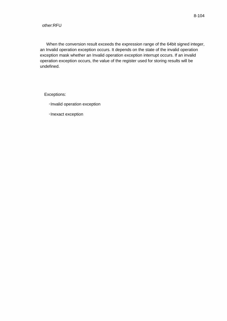
8-104
other:RFU
When the conversion result exceeds the expression range of the 64bit signed integer,
an Invalid operation exception occurs. It depends on the state of the invalid operation
exception mask whether an Invalid operation exception interrupt occurs. If an invalid
operation exception occurs, the value of the register used for storing results will be
undefined.
Exceptions:
・Invalid operation exception
・Inexact exception
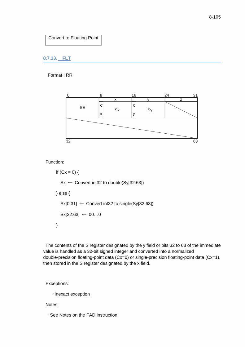
8-105
Convert to Floating Point
8.7.13. FLT
Format : RR
x
5E Sx Sy
y
C
y
z8 16 24 31
32 63
0
C
x
Function:
if (Cx = 0) {
Sx ← Convert int32 to double(Sy[32:63])
} else {
Sx[0:31] ← Convert int32 to single(Sy[32:63])
Sx[32:63] ← 00…0
}
The contents of the S register designated by the y field or bits 32 to 63 of the immediate
value is handled as a 32-bit signed integer and converted into a normalized
double-precision floating-point data (Cx=0) or single-precision floating-point data (Cx=1),
then stored in the S register designated by the x field.
Exceptions:
・Inexact exception
Notes:
・See Notes on the FAD instruction.
8-106
Convert to Floating Point
8.7.14. FLTX
Format : RR
x
5F Sx Sy
y
C
y
z8 16 24 31
32 63
0
Function:
Sx ← Convert int64 to double(Sy)
The contents of the S register designated by the y field or the immediate value is
handled as a 64-bit signed integer and converted into a normalized double-precision
floating-point data. The result is then stored in the S register designated by the x field.
Exceptions:
・Inexact exception
Notes:
・See Notes on the FAD instruction.
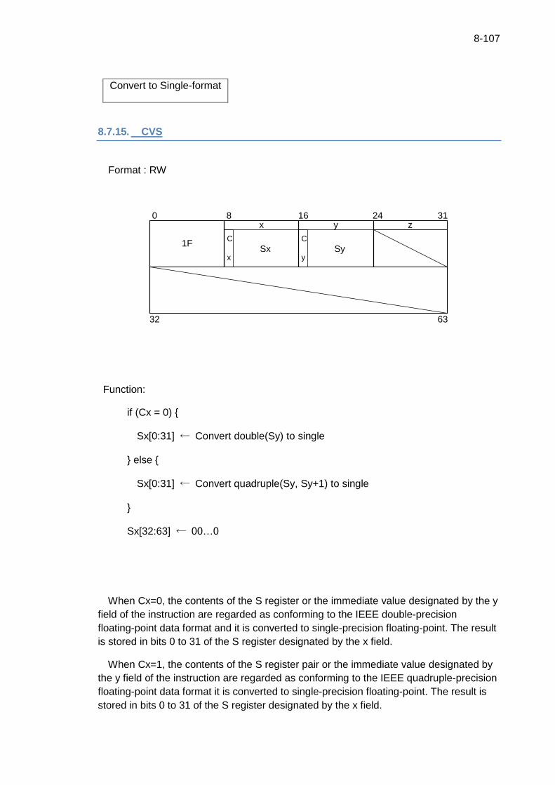
8-107
Convert to Single-format
8.7.15. CVS
Format : RW
x
1F Sx Sy
y
C
y
z8 16 24 31
32 63
0
C
x
Function:
if (Cx = 0) {
Sx[0:31] ← Convert double(Sy) to single
} else {
Sx[0:31] ← Convert quadruple(Sy, Sy+1) to single
}
Sx[32:63] ← 00…0
When Cx=0, the contents of the S register or the immediate value designated by the y
field of the instruction are regarded as conforming to the IEEE double-precision
floating-point data format and it is converted to single-precision floating-point. The result
is stored in bits 0 to 31 of the S register designated by the x field.
When Cx=1, the contents of the S register pair or the immediate value designated by
the y field of the instruction are regarded as conforming to the IEEE quadruple-precision
floating-point data format it is converted to single-precision floating-point. The result is
stored in bits 0 to 31 of the S register designated by the x field.
8-108
It stores zeros in bits 32 to 63 bits of the Sx in both cases.
During conversion, the mantissa is rounded according to the PSW rounding
specification.
An S register pair refers to two consecutive S registers starting with an even-numbered
S register. That is, the y field must designate even-numbered S registers. Otherwise, an
illegal instruction format exception occurs.
Exceptions:
・Floating-point overflow exception
・Floating-point underflow exception
・Invalid operation exception
・Inexact exception
Notes:
・See Notes on the FAD and FAQ instructions.
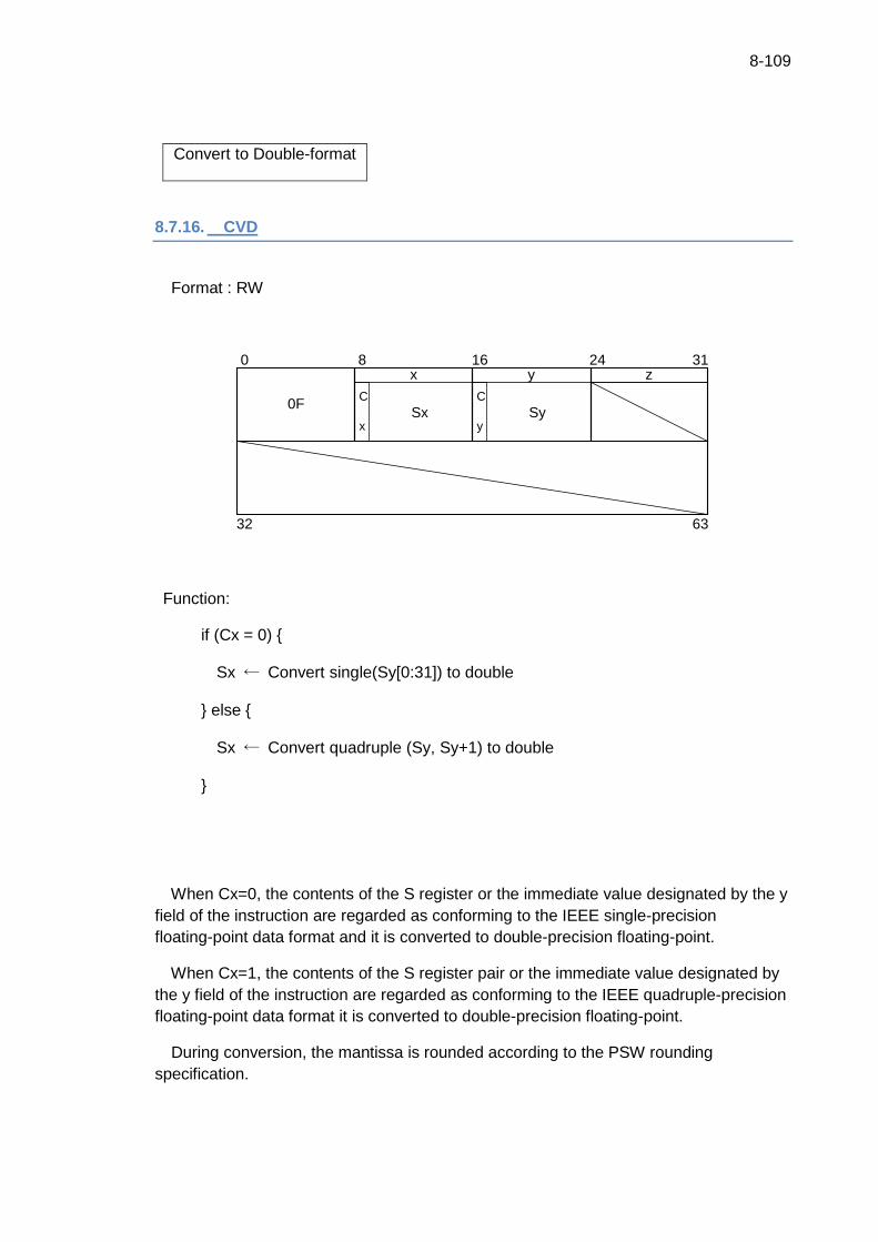
8-109
Convert to Double-format
8.7.16. CVD
Format : RW
x
0F Sx Sy
y
C
y
z8 16 24 31
32 63
0
C
x
Function:
if (Cx = 0) {
Sx ← Convert single(Sy[0:31]) to double
} else {
Sx ← Convert quadruple (Sy, Sy+1) to double
}
When Cx=0, the contents of the S register or the immediate value designated by the y
field of the instruction are regarded as conforming to the IEEE single-precision
floating-point data format and it is converted to double-precision floating-point.
When Cx=1, the contents of the S register pair or the immediate value designated by
the y field of the instruction are regarded as conforming to the IEEE quadruple-precision
floating-point data format it is converted to double-precision floating-point.
During conversion, the mantissa is rounded according to the PSW rounding
specification.
8-110
An S register pair refers to two consecutive S registers starting with an even-numbered
S register. That is, the y field must designate even-numbered S registers. Otherwise, an
illegal instruction format exception occurs.
Exceptions:
・Floating-point overflow exception
・Floating-point underflow exception
・Invalid operation exception
・Inexact exception
Notes:
・See Notes on the FAD and FAQ instructions.
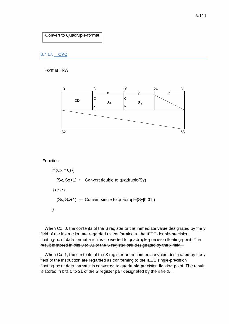
8-111
Convert to Quadruple-format
8.7.17. CVQ
Format : RW
x
2D Sx Sy
y
C
y
z8 16 24 31
32 63
0
C
x
Function:
if (Cx = 0) {
(Sx, Sx+1) ← Convert double to quadruple(Sy)
} else {
(Sx, Sx+1) ← Convert single to quadruple(Sy[0:31])
}
When Cx=0, the contents of the S register or the immediate value designated by the y
field of the instruction are regarded as conforming to the IEEE double-precision
floating-point data format and it is converted to quadruple-precision floating-point. The
result is stored in bits 0 to 31 of the S register pair designated by the x field.
When Cx=1, the contents of the S register or the immediate value designated by the y
field of the instruction are regarded as conforming to the IEEE single-precision
floating-point data format it is converted to quadruple-precision floating-point. The result
is stored in bits 0 to 31 of the S register pair designated by the x field.
8-112
An S register pair refers to two consecutive S registers starting with an even-numbered
S register. That is, the x field must designate even-numbered S registers. Otherwise, an
illegal instruction format exception occurs.
Exceptions:
・Invalid operation exception
Notes:
・See Notes on the FAD and FAQ instructions.
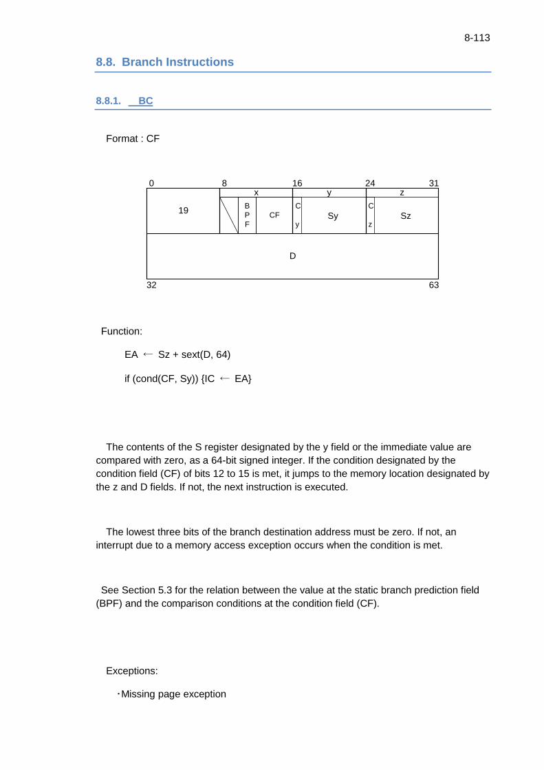
8-113
8.8. Branch Instructions
8.8.1. BC
Format : CF
x
19 Sy Sz
y
C
y
z
C
z
8 16 24 31
D
32 63
0
B
P
F
CF
Function:
EA ← Sz + sext(D, 64)
if (cond(CF, Sy)) {IC ← EA}
The contents of the S register designated by the y field or the immediate value are
compared with zero, as a 64-bit signed integer. If the condition designated by the
condition field (CF) of bits 12 to 15 is met, it jumps to the memory location designated by
the z and D fields. If not, the next instruction is executed.
The lowest three bits of the branch destination address must be zero. If not, an
interrupt due to a memory access exception occurs when the condition is met.
See Section 5.3 for the relation between the value at the static branch prediction field
(BPF) and the comparison conditions at the condition field (CF).
Exceptions:
・Missing page exception
8-114
・Missing space exception
・Memory access exception
・Branch trap
Notes:
・When Cz=0, an immediate value of 0 is formed into the z operand irrespective of Sz
value.
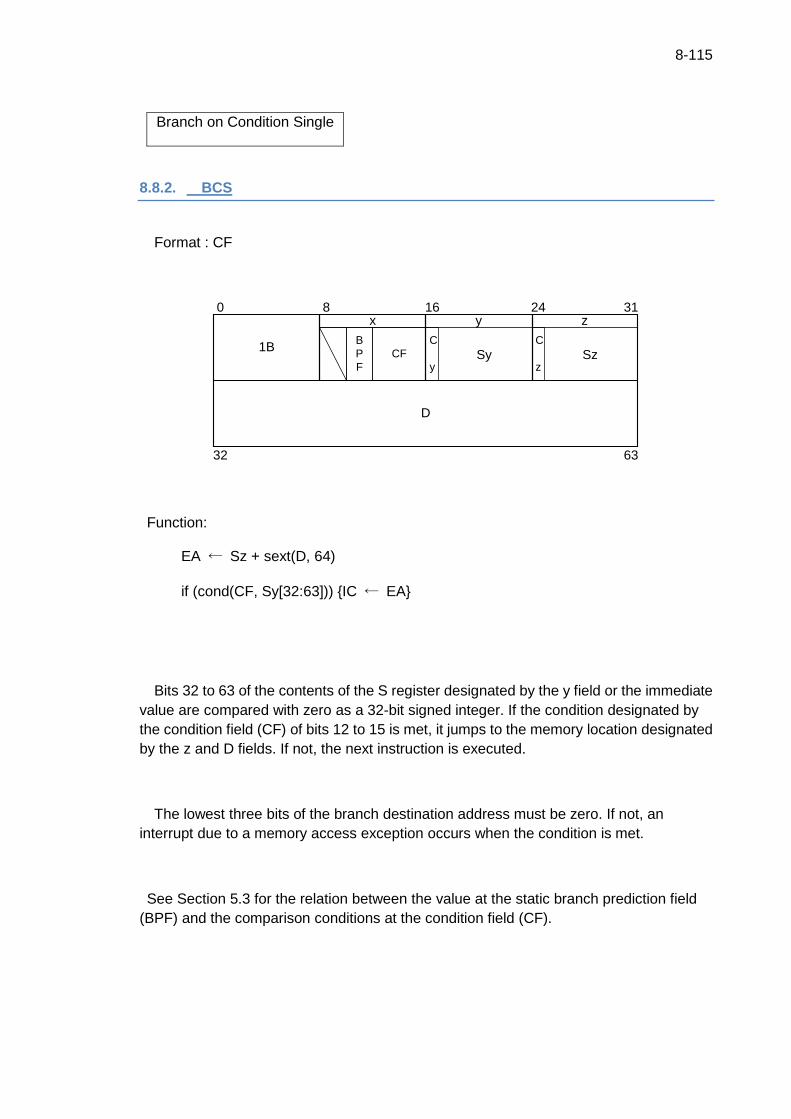
8-115
Branch on Condition Single
8.8.2. BCS
Format : CF
x
1B Sy Sz
y
C
y
z
C
z
8 16 24 31
D
32 63
0
B
P
F
CF
Function:
EA ← Sz + sext(D, 64)
if (cond(CF, Sy[32:63])) {IC ← EA}
Bits 32 to 63 of the contents of the S register designated by the y field or the immediate
value are compared with zero as a 32-bit signed integer. If the condition designated by
the condition field (CF) of bits 12 to 15 is met, it jumps to the memory location designated
by the z and D fields. If not, the next instruction is executed.
The lowest three bits of the branch destination address must be zero. If not, an
interrupt due to a memory access exception occurs when the condition is met.
See Section 5.3 for the relation between the value at the static branch prediction field
(BPF) and the comparison conditions at the condition field (CF).
8-116
Exceptions:
・Missing page exception
・Missing space exception
・Memory access exception
・Branch trap
Notes:
・When Cz=0, an immediate value of 0 is formed into the z operand irrespective of Sz
value.
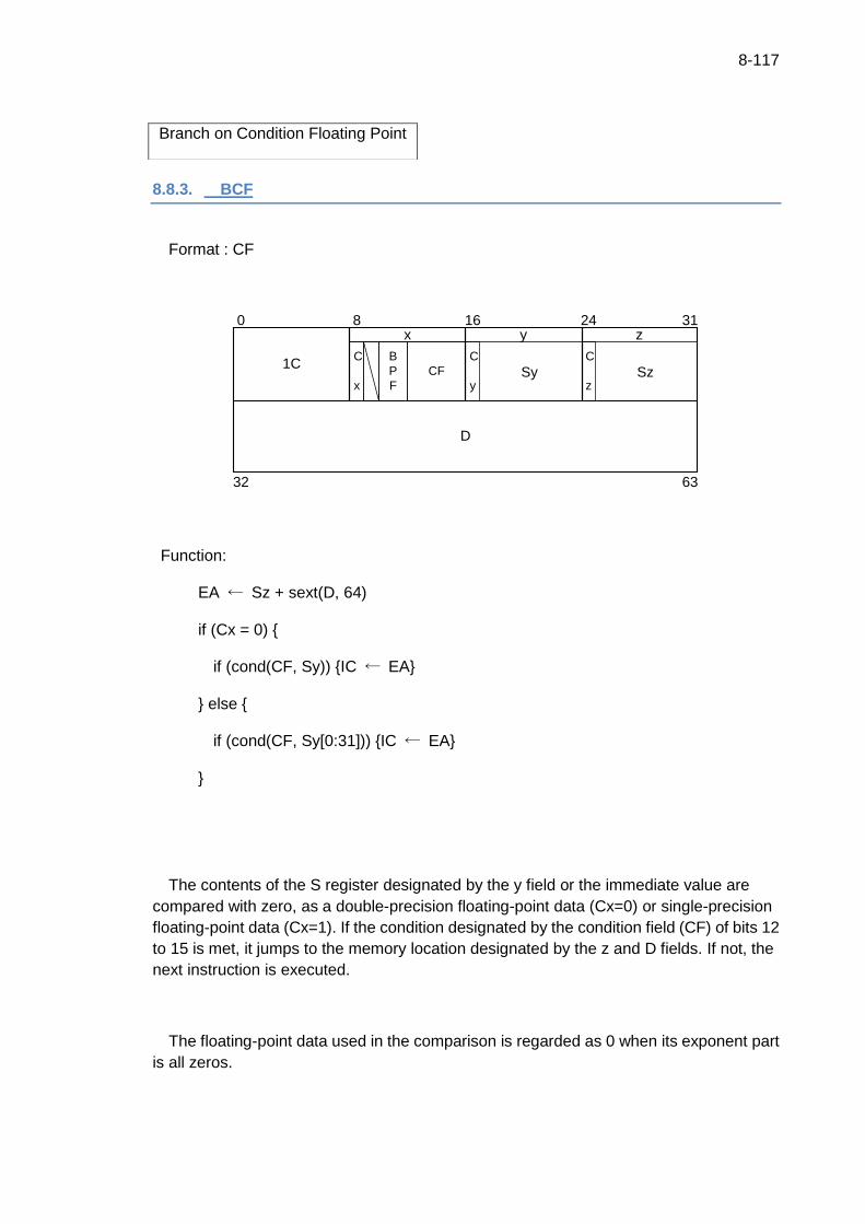
8-117
8.8.3. BCF
Format : CF
x
1C Sy Sz
y
C
y
z
C
z
8 16 24 31
D
32 63
0
C
x
B
P
F
CF
Function:
EA ← Sz + sext(D, 64)
if (Cx = 0) {
if (cond(CF, Sy)) {IC ← EA}
} else {
if (cond(CF, Sy[0:31])) {IC ← EA}
}
The contents of the S register designated by the y field or the immediate value are
compared with zero, as a double-precision floating-point data (Cx=0) or single-precision
floating-point data (Cx=1). If the condition designated by the condition field (CF) of bits 12
to 15 is met, it jumps to the memory location designated by the z and D fields. If not, the
next instruction is executed.
The floating-point data used in the comparison is regarded as 0 when its exponent part
is all zeros.
Branch on Condition Floating Point
8-118
The lowest three bits of the branch destination address must be zero. If not, an
interrupt due to a memory access exception occurs when the condition is met.
See Section 5.3 for the relation between the value at the static branch prediction field
(BPF) and the comparison conditions at the condition field (CF).
Exceptions:
・Missing page exception
・Missing space exception
・Memory access exception
・Branch trap
Notes:
・When Cz=0, an immediate value of 0 is formed into the z operand irrespective of Sz
value.
8-119
Branch on Condition Relative
8.8.4. BCR
Format : CF
x
18 Sy Sz
y
C
y
z
C
z
8 16 24 31
D
32 63
0
C
x
C
x
2
B
P
F
CF
Function:
if ((Cx = 0) & (Cx2 = 0)) {
if (cond(CF, Sy, Sz)) {IC ← IC + sext(D, 64)}
} else if ((Cx = 1) & (Cx2 = 0)) {
if (cond(CF, Sy[32:63], Sz[32:63])) {IC ← IC + sext(D, 64)}
} else if ((Cx = 0) & (Cx2 = 1)) {
if (cond(CF, Sy, Sz)) {IC ← IC + sext(D, 64)}
} else if ((Cx = 1) & (Cx2 = 1)) {
if (cond(CF, Sy[0:31], Sz[0:31])) { IC ← IC + sext(D, 64)}
}
The contents of the S register designated by the y field or the immediate value are
compared with the contents of the S register designated by the z field or the immediate
value. If the condition designated by the condition field (CF) of bits 12 to 15 is met, the
control branches to the memory location designated by the z and D fields. If not, the next
instruction is executed.
8-120
When Cx=0 and Cx2=0, Sy is compared with Sz as a 64-bit signed integer.
When Cx=1 and Cx2=0, Sy is compared with Sz as a 32-bit signed integer.
When Cx=0 and Cx2=1, Sy is compared with Sz as a double-precision floating-point
data.
When Cx=1 and Cx2=1, Sy is compared with Sz as a single-precision floating-point
data.
The floating-point data tested in the comparison is regarded as 0 when its exponent
part is all zero.
The lowest three bits of the branch destination address must be zero. If not, an
interrupt due to a memory access exception occurs when the condition is met.
See Section 5.3 for the relation between the value at the static branch prediction field
(BPF) and the comparison conditions at the condition field (CF).

8-121
Exceptions:
・Missing page exception
・Missing space exception
・Memory access exception
・Branch trap
Notes:
・When Cz=0, an immediate value of 0 is formed into the z operand irrespective of Sz
value.
8-122
Branch and Save IC
8.8.5. BSIC
Format : RM
x
08 Sx Sy Sz
y
C
y
z
C
z
8 16 24 31
D
32 63
0
Function:
EA ← Sy + Sz + sext(D, 64)
Sx ← IC + 8
IC ← EA
The current instruction counter (IC) for the BSIC instruction + 8 is saved to bits 0 to 63 of
the S register designated by the x field. Then it jumps to the memory location designated
by the y, z, and D fields of the instruction.
The lowest three bits of the branch destination address must be zero. If not, an
interrupt due to a memory access exception occurs.
Exceptions:
・Missing page exception
・Missing space exception
・Memory access exception
・Branch trap
8-123
Notes:
・As memory addresses, only 48 bits are effective in Aurora. The upper 16 bits of Sx
are always set to zero by this operation.
・When Cz=0, an immediate value of 0 is formed into the z operand irrespective of Sz
value.
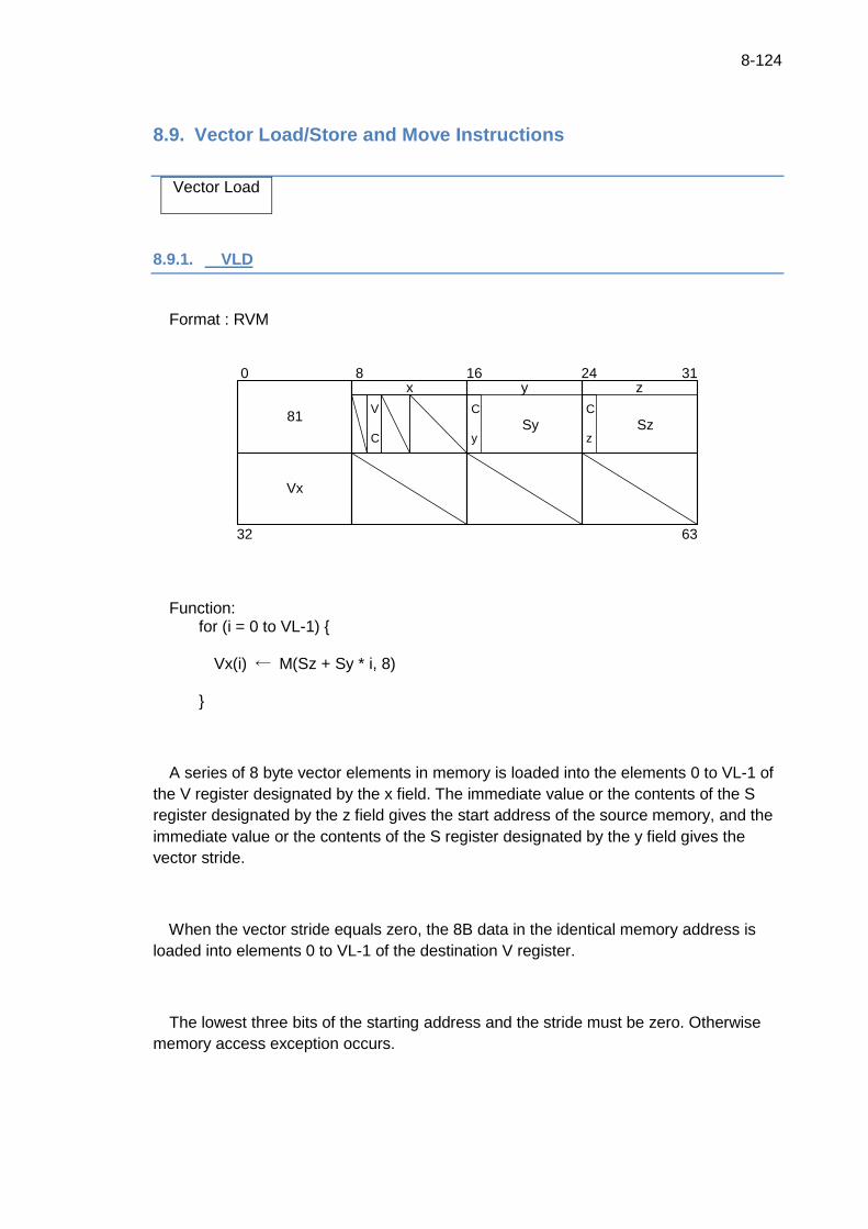
8-124
8.9. Vector Load/Store and Move Instructions
Vector Load
8.9.1. VLD
Format : RVM
x
81 Sy Sz
y
C
y
z
C
z
8 16 24 31
32 63
0
Vx
V
C
Function: for (i = 0 to VL-1) {
Vx(i) ← M(Sz + Sy * i, 8)
}
A series of 8 byte vector elements in memory is loaded into the elements 0 to VL-1 of
the V register designated by the x field. The immediate value or the contents of the S
register designated by the z field gives the start address of the source memory, and the
immediate value or the contents of the S register designated by the y field gives the
vector stride.
When the vector stride equals zero, the 8B data in the identical memory address is
loaded into elements 0 to VL-1 of the destination V register.
The lowest three bits of the starting address and the stride must be zero. Otherwise
memory access exception occurs.
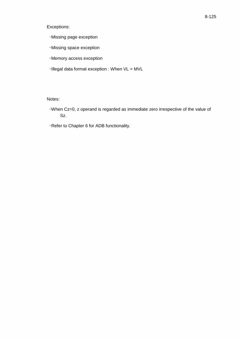
8-125
Exceptions:
・Missing page exception
・Missing space exception
・Memory access exception
・Illegal data format exception : When VL > MVL
Notes:
・When Cz=0, z operand is regarded as immediate zero irrespective of the value of
Sz.
・Refer to Chapter 6 for ADB functionality.
8-126
Vector Load Upper
8.9.2. VLDU
Format : RVM
x
82 Sy Sz
y
C
y
z
C
z
8 16 24 31
32 63
0
Vx
V
C
Function: for (i = 0 to VL-1) {
Vx(i)[0:31] ← M(Sz + Sy * i, 4)
Vx(i)[32:63] ← 00…0
}
A series of 4 byte vector elements in memory is loaded into bits 0 to 31 of the elements
0 to VL-1 of the V register designated by the x field. The immediate value or the contents
of the S register designated by the z field gives the start address of the source memory,
and the immediate value or the contents of the S register designated by the y field gives
the vector stride. Bits 32 to 63 of elements 0 to VL of the destination V register are filled
with zeros.
When the vector stride equals zero, the 4B data in the identical memory address is
loaded into elements 0 to VL-1 of the destination V register.
The lowest two bits of the starting address and the stride must be zero. Otherwise
memory access exception occurs.

8-127
Exceptions:
・Missing page exception
・Missing space exception
・Memory access exception
・Illegal data format exception : When VL > MVL
Notes:
・When Cz=0, z operand is regarded as immediate zero irrespective of the value of
Sz.
・Refer to Chapter 6 for ADB functionality.
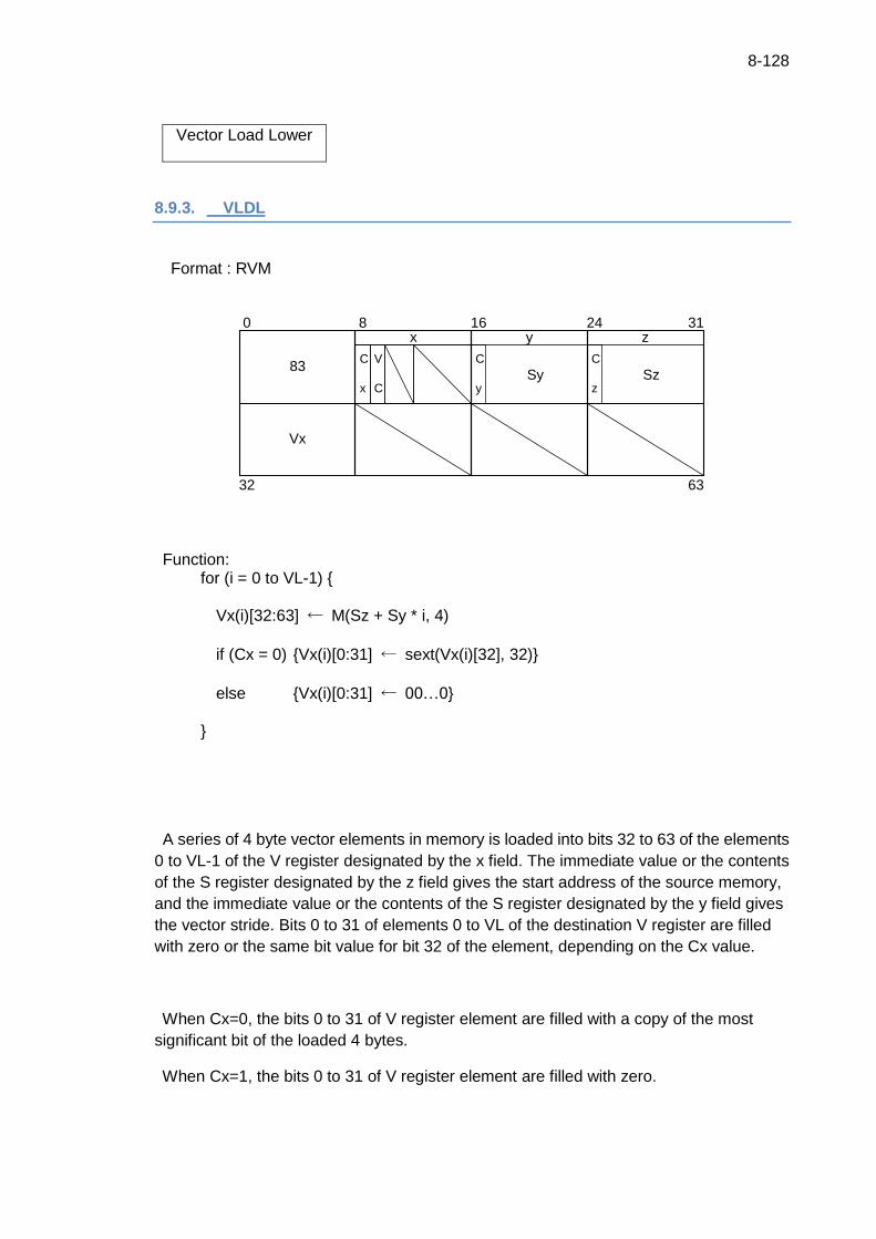
8-128
Vector Load Lower
8.9.3. VLDL
Format : RVM
x
83 Sy Sz
y
C
y
z
C
z
8 16 24 31
32 63
0
Vx
V
C
C
x
Function: for (i = 0 to VL-1) {
Vx(i)[32:63] ← M(Sz + Sy * i, 4)
if (Cx = 0) {Vx(i)[0:31] ← sext(Vx(i)[32], 32)}
else {Vx(i)[0:31] ← 00…0}
}
A series of 4 byte vector elements in memory is loaded into bits 32 to 63 of the elements
0 to VL-1 of the V register designated by the x field. The immediate value or the contents
of the S register designated by the z field gives the start address of the source memory,
and the immediate value or the contents of the S register designated by the y field gives
the vector stride. Bits 0 to 31 of elements 0 to VL of the destination V register are filled
with zero or the same bit value for bit 32 of the element, depending on the Cx value.
When Cx=0, the bits 0 to 31 of V register element are filled with a copy of the most
significant bit of the loaded 4 bytes.
When Cx=1, the bits 0 to 31 of V register element are filled with zero.
8-129
When the vector stride equals zero, the 4B data in the identical memory address is
loaded into elements 0 to VL-1 of the destination V register.
The lowest two bits of the starting address and the stride must be zero. Otherwise
memory access exception occurs.
Exceptions:
・Missing page exception
・Missing space exception
・Memory access exception
・Illegal data format exception : When VL > MVL
Notes:
・When Cz=0, z operand is regarded as immediate zero irrespective of the value of
Sz.
・Refer to Chapter 6 for ADB functionality.
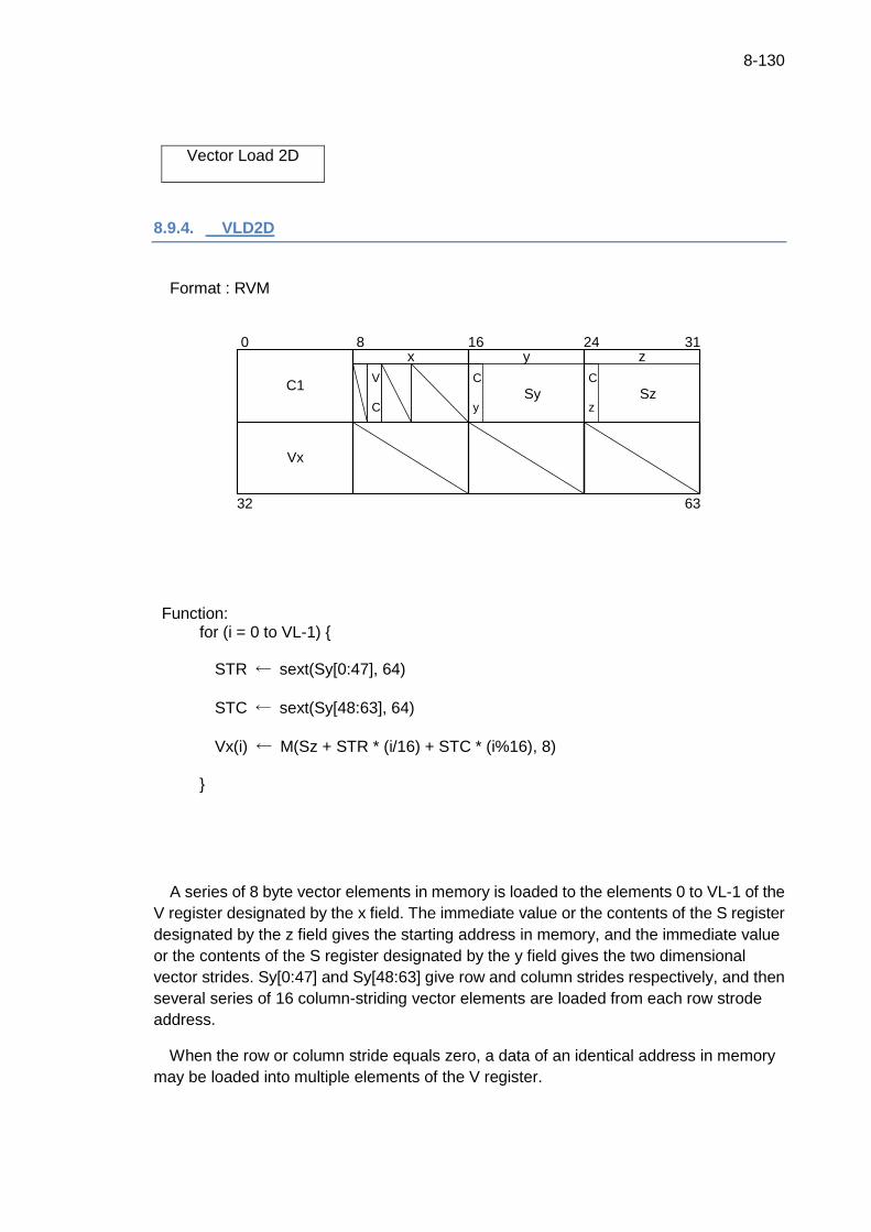
8-130
Vector Load 2D
8.9.4. VLD2D
Format : RVM
x
C1 Sy Sz
y
C
y
z
C
z
8 16 24 31
32 63
0
Vx
V
C
Function: for (i = 0 to VL-1) {
STR ← sext(Sy[0:47], 64)
STC ← sext(Sy[48:63], 64)
Vx(i) ← M(Sz + STR * (i/16) + STC * (i%16), 8)
}
A series of 8 byte vector elements in memory is loaded to the elements 0 to VL-1 of the
V register designated by the x field. The immediate value or the contents of the S register
designated by the z field gives the starting address in memory, and the immediate value
or the contents of the S register designated by the y field gives the two dimensional
vector strides. Sy[0:47] and Sy[48:63] give row and column strides respectively, and then
several series of 16 column-striding vector elements are loaded from each row strode
address.
When the row or column stride equals zero, a data of an identical address in memory
may be loaded into multiple elements of the V register.
8-131
The lowest three bits of the starting address and both the row and column stride must
be zero. Otherwise memory access exception occurs.
Exceptions:
・Missing page exception
・Missing space exception
・Memory access exception
・Illegal data format exception : When VL > MVL
Notes:
・When Cz=0, z operand is regarded as immediate zero irrespective of Sz.
・See also Chapter 6 for ADB functionality.
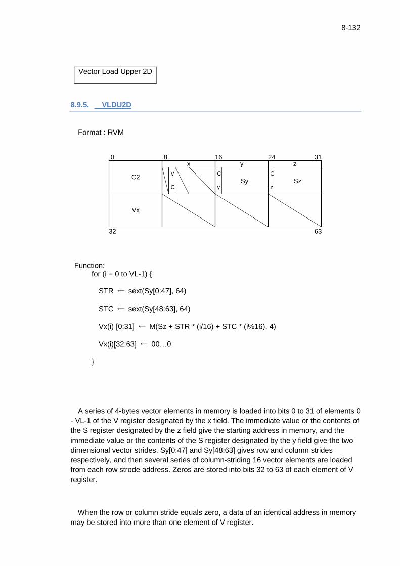
8-132
Vector Load Upper 2D
8.9.5. VLDU2D
Format : RVM
x
C2 Sy Sz
y
C
y
z
C
z
8 16 24 31
32 63
0
Vx
V
C
Function: for (i = 0 to VL-1) {
STR ← sext(Sy[0:47], 64)
STC ← sext(Sy[48:63], 64)
Vx(i) [0:31] ← M(Sz + STR * (i/16) + STC * (i%16), 4)
Vx(i)[32:63] ← 00…0
}
A series of 4-bytes vector elements in memory is loaded into bits 0 to 31 of elements 0
- VL-1 of the V register designated by the x field. The immediate value or the contents of
the S register designated by the z field give the starting address in memory, and the
immediate value or the contents of the S register designated by the y field give the two
dimensional vector strides. Sy[0:47] and Sy[48:63] gives row and column strides
respectively, and then several series of column-striding 16 vector elements are loaded
from each row strode address. Zeros are stored into bits 32 to 63 of each element of V
register.
When the row or column stride equals zero, a data of an identical address in memory
may be stored into more than one element of V register.
8-133
The lowest two bits of the starting address and both the row and column stride must be
zero. Otherwise memory access exception occurs.
Exceptions:
・Missing page exception
・Missing space exception
・Memory access exception
・Illegal data format exception : When VL > MVL
Notes:
・When Cz=0, z operand is the immediate value of zero irrespective of the value of Sz.
・Refer to an item of ADB of Chapter 6 about a use presence of ADB.
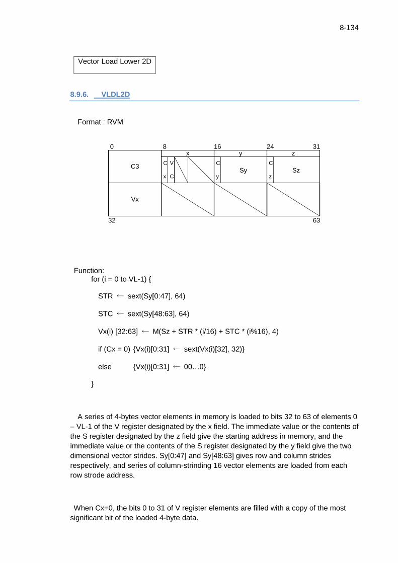
8-134
Vector Load Lower 2D
8.9.6. VLDL2D
Format : RVM
x
C3 Sy Sz
y
C
y
z
C
z
8 16 24 31
32 63
0
Vx
V
C
C
x
Function: for (i = 0 to VL-1) {
STR ← sext(Sy[0:47], 64)
STC ← sext(Sy[48:63], 64)
Vx(i) [32:63] ← M(Sz + STR * (i/16) + STC * (i%16), 4)
if (Cx = 0) {Vx(i)[0:31] ← sext(Vx(i)[32], 32)}
else {Vx(i)[0:31] ← 00…0}
}
A series of 4-bytes vector elements in memory is loaded to bits 32 to 63 of elements 0
– VL-1 of the V register designated by the x field. The immediate value or the contents of
the S register designated by the z field give the starting address in memory, and the
immediate value or the contents of the S register designated by the y field give the two
dimensional vector strides. Sy[0:47] and Sy[48:63] gives row and column strides
respectively, and series of column-strinding 16 vector elements are loaded from each
row strode address.
When Cx=0, the bits 0 to 31 of V register elements are filled with a copy of the most
significant bit of the loaded 4-byte data.
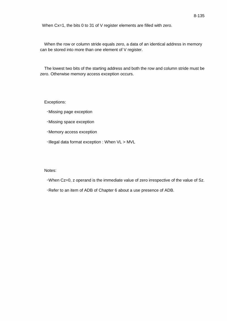
8-135
When Cx=1, the bits 0 to 31 of V register elements are filled with zero.
When the row or column stride equals zero, a data of an identical address in memory
can be stored into more than one element of V register.
The lowest two bits of the starting address and both the row and column stride must be
zero. Otherwise memory access exception occurs.
Exceptions:
・Missing page exception
・Missing space exception
・Memory access exception
・Illegal data format exception : When VL > MVL
Notes:
・When Cz=0, z operand is the immediate value of zero irrespective of the value of Sz.
・Refer to an item of ADB of Chapter 6 about a use presence of ADB.
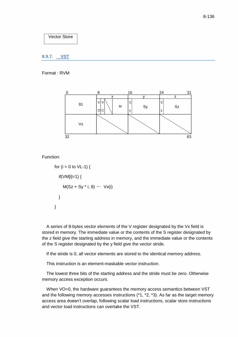
8-136
Vector Store
8.9.7. VST
Format : RVM
x
91 Sy Sz
y
C
y
z
C
z
8 16 24 31
32 63
0
Vx
V
C
V
O
M
Function:
for (i = 0 to VL-1) {
if(VM[i]=1) {
M(Sz + Sy * i, 8) ← Vx(i)
}
}
A series of 8-bytes vector elements of the V register designated by the Vx field is
stored in memory. The immediate value or the contents of the S register designated by
the z field give the starting address in memory, and the immediate value or the contents
of the S register designated by the y field give the vector stride.
If the stride is 0, all vector elements are stored to the identical memory address.
This instruction is an element-maskable vector instruction.
The lowest three bits of the starting address and the stride must be zero. Otherwise
memory access exception occurs.
When VO=0, the hardware guarantees the memory access semantics between VST
and the following memory accesses instructions (*1, *2, *3). As far as the target memory
access area doesn’t overlap, following scalar load instructions, scalar store instructions
and vector load instructions can overtake the VST.
8-137
When VO=1, the hardware does not guarantee the memory access sequence between
VST and the following memory accesses (*1,*2,*3) until SVOB appears in the instruction
sequence. The hardware may give execution priority to the memory accesses (*1, *2, *3)
following the VST. Since hardware doesn’t see address dependencies between the VST
and the followers before SVOB, software must take care of it to avoid unexpected side
effect to occur. And also, it is not always guaranteed to give priority to following scalar
load instructions, scalar store instructions and vector load instructions.
Exceptions:
・Memory protection exception
・Missing page exception
・Missing space exception
・Memory access exception
・Illegal data format exception : When VL > MVL
Notes:
・When Cz=0, z operand is the immediate value of zero irrespective of the value of
Sz.
・Refer to an item of ADB of Chapter 6 about a use presence of ADB.
・Refer to SVOB instruction.
・ *1 : LDS,LDU,LDL,LD1B,LD2B,DLDS,DLDU,DLDL,PFCH
・ *2 : STS,STU,STL,ST1B,ST2B
・ *3 : VLD,VLDU,VLDL,VLD2D,VLDU2D,VLDL2D, VGT,VGTU,VGTL,PFCHV
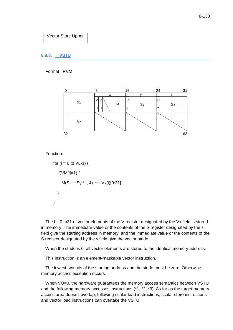
8-138
Vector Store Upper
8.9.8. VSTU
Format : RVM
x
92 Sy Sz
y
C
y
z
C
z
8 16 24 31
32 63
0
Vx
V
C
V
O
M
Function:
for (i = 0 to VL-1) {
if(VM[i]=1) {
M(Sz + Sy * i, 4) ← Vx(i)[0:31]
}
}
The bit 0 to31 of vector elements of the V register designated by the Vx field is stored
in memory. The immediate value or the contents of the S register designated by the z
field give the starting address in memory, and the immediate value or the contents of the
S register designated by the y field give the vector stride.
When the stride is 0, all vector elements are stored to the identical memory address.
This instruction is an element-maskable vector instruction.
The lowest two bits of the starting address and the stride must be zero. Otherwise
memory access exception occurs.
When VO=0, the hardware guarantees the memory access semantics between VSTU
and the following memory accesses instructions (*1, *2, *3). As far as the target memory
access area doesn’t overlap, following scalar load instructions, scalar store instructions
and vector load instructions can overtake the VSTU.
8-139
When VO=1, the hardware does not guarantee the memory access sequence between
VSTU and the following memory accesses (*1,*2,*3) until SVOB appears in the
instruction sequence. The hardware may give execution priority to the memory accesses
(*1, *2, *3) following the VSTU. Since hardware doesn’t see address dependencies
between the VSTU and the followers before SVOB, software must take care of it to avoid
unexpected side effect to occur. And also, it is not always guaranteed to give priority to
following scalar load instructions, scalar store instructions and vector load instructions.
Exceptions:
・Memory protection exception
・Missing page exception
・Missing space exception
・Memory access exception
・Illegal data format exception : When VL > MVL
Notes:
・When Cz=0, z operand is the immediate value of zero irrespective of the value of
Sz.
・Refer to an item of ADB of Chapter 6 about a use presence of ADB.
・Refer to SVOB instruction.
・ *1 : LDS,LDU,LDL,LD1B,LD2B,DLDS,DLDU,DLDL,PFCH
・ *2 : STS,STU,STL,ST1B,ST2B
・ *3 : VLD,VLDU,VLDL,VLD2D,VLDU2D,VLDL2D,VGT,VGTU,VGTL,PFCHV

8-140
Vector Store Lower
8.9.9. VSTL
Format : RVM
x
93 Sy Sz
y
C
y
z
C
z
8 16 24 31
32 63
0
Vx
V
C
V
O
M
Function:
for (i = 0 to VL-1) {
if(VM[i]=1) {
M(Sz + Sy * i, 4) ← Vx(i)[32:63]
}
}
The bit 32 to 63 of vector elements of the V register designated by the Vx field is stored
in memory. The immediate value or the contents of the S register designated by the z
field give the starting address in memory, and the immediate value or the contents of the
S register designated by the y field give the vector stride.
If the stride is 0, all vector elements are stored to the identical memory address.
This instruction is an element-maskable vector instruction.
The lowest two bits of the starting address and the stride must be zero. Otherwise
memory access exception occurs.
When VO=0, the hardware guarantees the memory access semantics between VSTL
and the following memory accesses instructions (*1, *2, *3). As far as the target memory
access area doesn’t overlap, following scalar load instructions, scalar store instructions
and vector load instructions can overtake the VSTL.
8-141
When VO=1, the hardware does not guarantee the memory access sequence between
VSTL and the following memory accesses (*1,*2,*3) until SVOB appears in the
instruction sequence. The hardware may give execution priority to the memory accesses
(*1, *2, *3) following the VSTL. Since hardware doesn’t see address dependencies
between the VSTL and the followers before SVOB, software must take care of it to avoid
unexpected side effect to occur. And also, it is not always guaranteed to give priority to
following scalar load instructions, scalar store instructions and vector load instructions.
Exceptions:
・Memory protection exception
・Missing page exception
・Missing space exception
・Memory access exception
・Illegal data format exception : When VL > MVL
Notes:
・When Cz=0, z operand is the immediate value of zero irrespective of the value of Sz.
・Refer to an item of ADB of Chapter 6 about a use presence of ADB.
・Refer to SVOB instruction.
・ *1 : LDS,LDU,LDL,LD1B,LD2B,DLDS,DLDU,DLDL,PFCH
・ *2 : STS,STU,STL,ST1B,ST2B
・ *3 : VLD,VLDU,VLDL,VLD2D,VLDU2D,VLDL2D,VGT,VGTU,VGTL,PFCHV
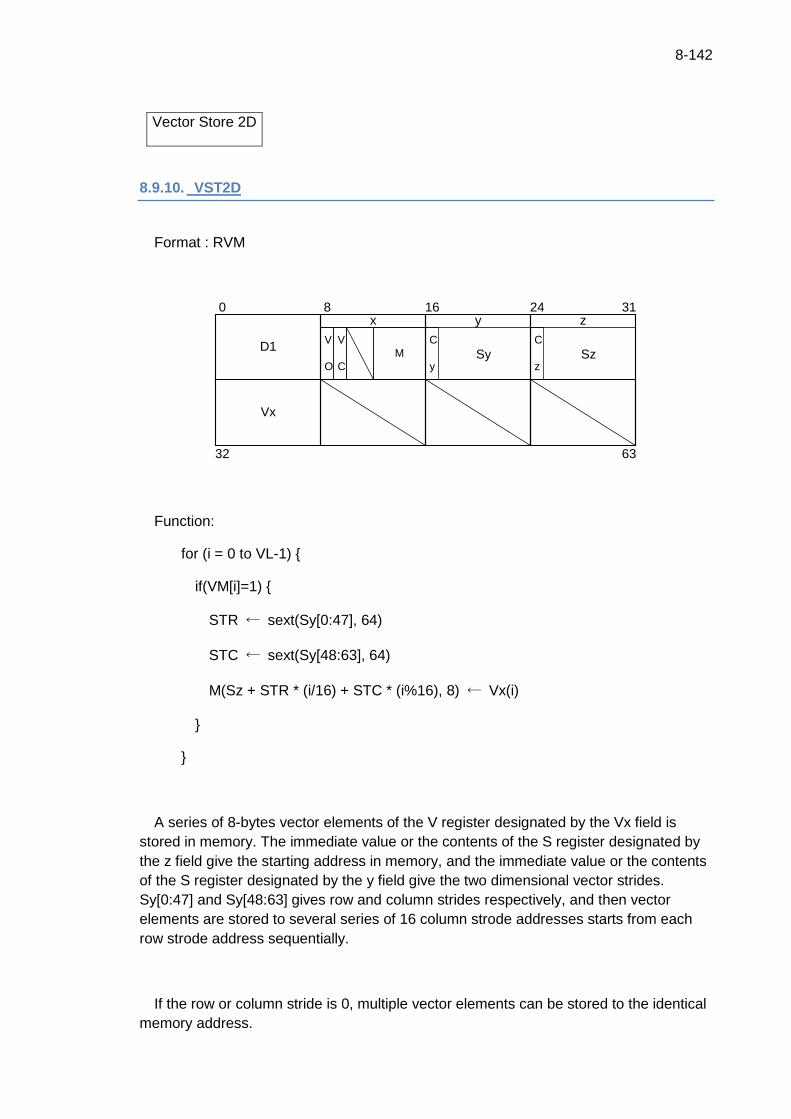
8-142
Vector Store 2D
8.9.10. VST2D
Format : RVM
x
D1 Sy Sz
y
C
y
z
C
z
8 16 24 31
32 63
0
Vx
V
C
V
O
M
Function:
for (i = 0 to VL-1) {
if(VM[i]=1) {
STR ← sext(Sy[0:47], 64)
STC ← sext(Sy[48:63], 64)
M(Sz + STR * (i/16) + STC * (i%16), 8) ← Vx(i)
}
}
A series of 8-bytes vector elements of the V register designated by the Vx field is
stored in memory. The immediate value or the contents of the S register designated by
the z field give the starting address in memory, and the immediate value or the contents
of the S register designated by the y field give the two dimensional vector strides.
Sy[0:47] and Sy[48:63] gives row and column strides respectively, and then vector
elements are stored to several series of 16 column strode addresses starts from each
row strode address sequentially.
If the row or column stride is 0, multiple vector elements can be stored to the identical
memory address.

8-143
This instruction is an element-maskable vector instruction.
The lowest three bits of the starting address and both the row and column stride must
be zero. Otherwise memory access exception occurs.
When VO=0, the hardware guarantees the memory access semantics between VST2D
and the following memory accesses instructions (*1, *2, *3). As far as the target memory
access area doesn’t overlap, following scalar load instructions, scalar store instructions
and vector load instructions can overtake the VST2D.
When VO=1, the hardware does not guarantee the memory access sequence between
VST2D and the following memory accesses (*1,*2,*3) until SVOB appears in the
instruction sequence. The hardware may give execution priority to the memory accesses
(*1, *2, *3) following the VST2D. Since hardware doesn’t see address dependencies
between the VST2D and the followers before SVOB, software must take care of it to
avoid unexpected side effect to occur. And also, it is not always guaranteed to give
priority to following scalar load instructions, scalar store instructions and vector load
instructions.
Exceptions:
・Memory protection exception
・Missing page exception
・Missing space exception
・Memory access exception
・Illegal data format exception : When VL > MVL
Notes:
・When Cz=0, z operand is the immediate value of zero irrespective of the value of
Sz.
・Refer to an item of ADB of Chapter 6 about a use presence of ADB.
・Refer to SVOB instruction.
・ *1 : LDS,LDU,LDL,LD1B,LD2B,DLDS,DLDU,DLDL,PFCH
・ *2 : STS,STU,STL,ST1B,ST2B
・ *3 : VLD,VLDU,VLDL,VLD2D,VLDU2D,VLDL2D,VGT,VGTU,VGTL,PFCHV
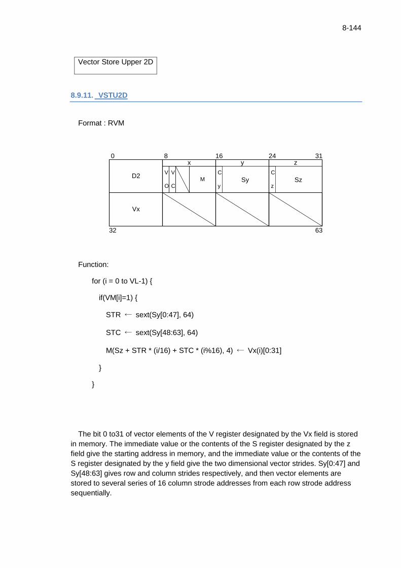
8-144
Vector Store Upper 2D
8.9.11. VSTU2D
Format : RVM
x
D2 Sy Sz
y
C
y
z
C
z
8 16 24 31
32 63
0
Vx
V
C
V
O
M
Function:
for (i = 0 to VL-1) {
if(VM[i]=1) {
STR ← sext(Sy[0:47], 64)
STC ← sext(Sy[48:63], 64)
M(Sz + STR * (i/16) + STC * (i%16), 4) ← Vx(i)[0:31]
}
}
The bit 0 to31 of vector elements of the V register designated by the Vx field is stored
in memory. The immediate value or the contents of the S register designated by the z
field give the starting address in memory, and the immediate value or the contents of the
S register designated by the y field give the two dimensional vector strides. Sy[0:47] and
Sy[48:63] gives row and column strides respectively, and then vector elements are
stored to several series of 16 column strode addresses from each row strode address
sequentially.
8-145
If the row or column stride is 0, multiple vector elements can be stored to the identical
memory address.
This instruction is an element-maskable vector instruction.
The lowest two bits of the starting address and both the row and column stride must be
zero. Otherwise memory access exception occurs.
When VO=0, the hardware guarantees the memory access semantics between
VSTU2D and the following memory accesses instructions (*1, *2, *3). As far as the target
memory access area doesn’t overlap, following scalar load instructions, scalar store
instructions and vector load instructions can overtake the VSTU2D.
When VO=1, the hardware does not guarantee the memory access sequence between
VSTU2D and the following memory accesses (*1,*2,*3) until SVOB appears in the
instruction sequence. The hardware may give execution priority to the memory accesses
(*1, *2, *3) following the VSTU2D. Since hardware doesn’t see address dependencies
between the VSTU2D and the followers before SVOB, software must take care of it to
avoid unexpected side effect to occur. And also, it is not always guaranteed to give
priority to following scalar load instructions, scalar store instructions and vector load
instructions.
Exceptions:
・Memory protection exception
・Missing page exception
・Missing space exception
・Memory access exception
・Illegal data format exception : When VL > MVL
Notes:
・When Cz=0, z operand is the immediate value of zero irrespective of the value of Sz.
・Refer to an item of ADB of Chapter 6 about a use presence of ADB.
・Refer to SVOB instruction.
・ *1 : LDS,LDU,LDL,LD1B,LD2B,DLDS,DLDU,DLDL,PFCH
・ *2 : STS,STU,STL,ST1B,ST2B
・ *3 : VLD,VLDU,VLDL,VLD2D,VLDU2D,VLDL2D,VGT,VGTU,VGTL,PFCHV
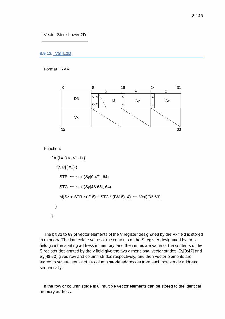
8-146
Vector Store Lower 2D
8.9.12. VSTL2D
Format : RVM
x
D3 Sy Sz
y
C
y
z
C
z
8 16 24 31
32 63
0
Vx
V
C
V
O
M
Function:
for (i = 0 to VL-1) {
if(VM[i]=1) {
STR ← sext(Sy[0:47], 64)
STC ← sext(Sy[48:63], 64)
M(Sz + STR * (i/16) + STC * (i%16), 4) ← Vx(i)[32:63]
}
}
The bit 32 to 63 of vector elements of the V register designated by the Vx field is stored
in memory. The immediate value or the contents of the S register designated by the z
field give the starting address in memory, and the immediate value or the contents of the
S register designated by the y field give the two dimensional vector strides. Sy[0:47] and
Sy[48:63] gives row and column strides respectively, and then vector elements are
stored to several series of 16 column strode addresses from each row strode address
sequentially.
If the row or column stride is 0, multiple vector elements can be stored to the identical
memory address.
8-147
This instruction is an element-maskable vector instruction.
The lowest two bits of the starting address and both the row and column stride must be
zero. Otherwise memory access exception occurs.
When VO=0, the hardware guarantees the memory access semantics between
VSTL2D and the following memory accesses instructions (*1, *2, *3). As far as the target
memory access area doesn’t overlap, following scalar load instructions, scalar store
instructions and vector load instructions can overtake the VSTL2D.
When VO=1, the hardware does not guarantee the memory access sequence between
VSTL2D and the following memory accesses (*1,*2,*3) until SVOB appears in the
instruction sequence. The hardware may give execution priority to the memory accesses
(*1, *2, *3) following the VSTL2D. Since hardware doesn’t see address dependencies
between the VSTL2D and the followers before SVOB, software must take care of it to
avoid unexpected side effect to occur. And also, it is not always guaranteed to give
priority to following scalar load instructions, scalar store instructions and vector load
instructions.
Exceptions:
・Memory protection exception
・Missing page exception
・Missing space exception
・Memory access exception
・Illegal data format exception : When VL > MVL
Notes:
・When Cz=0, z operand is the immediate value of zero irrespective of the value of
Sz.
・Refer to an item of ADB of Chapter 6 about a use presence of ADB.
・Refer to SVOB instruction.
・ *1 : LDS,LDU,LDL,LD1B,LD2B,DLDS,DLDU,DLDL,PFCH
・ *2 : STS,STU,STL,ST1B,ST2B
・ *3 : VLD,VLDU,VLDL,VLD2D,VLDU2D,VLDL2D,VGT,VGTU,VGTL,PFCHV
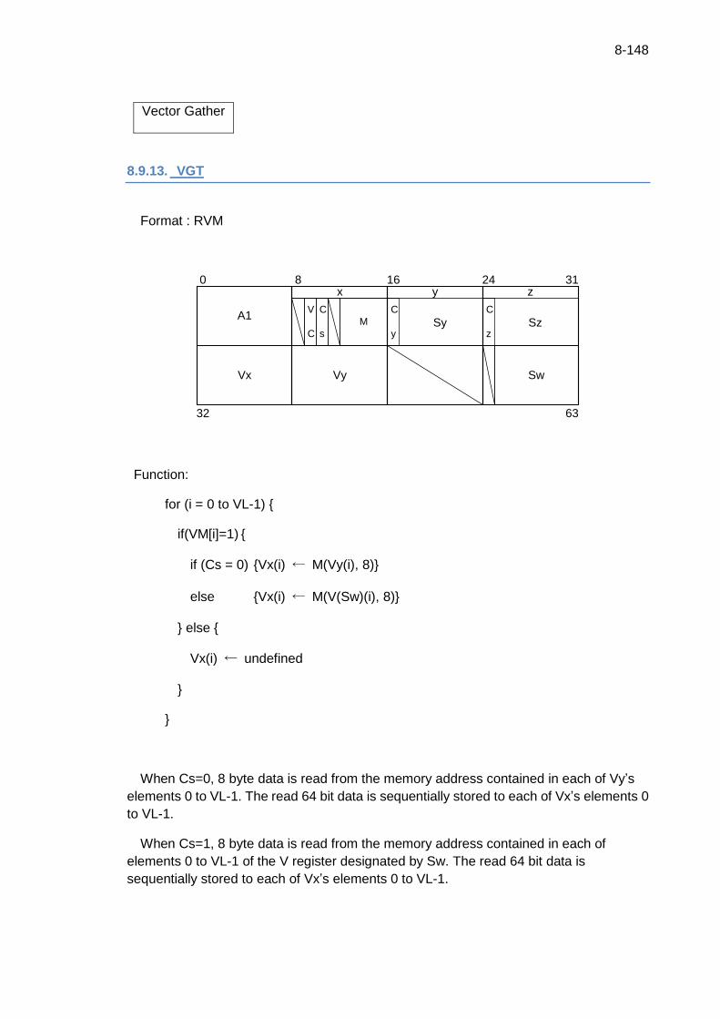
8-148
Vector Gather
8.9.13. VGT
Format : RVM
x
A1 Sy Sz
y
C
y
z
C
z
8 16 24 31
32 63
0
Vx Vy
V
C
M
C
s
Sw
Function:
for (i = 0 to VL-1) {
if(VM[i]=1) {
if (Cs = 0) {Vx(i) ← M(Vy(i), 8)}
else {Vx(i) ← M(V(Sw)(i), 8)}
} else {
Vx(i) ← undefined
}
}
When Cs=0, 8 byte data is read from the memory address contained in each of Vy’s
elements 0 to VL-1. The read 64 bit data is sequentially stored to each of Vx’s elements 0
to VL-1.
When Cs=1, 8 byte data is read from the memory address contained in each of
elements 0 to VL-1 of the V register designated by Sw. The read 64 bit data is
sequentially stored to each of Vx’s elements 0 to VL-1.
8-149
This instruction is an element-maskable vector instruction.An undefined value may be
loaded to the Vx[i] element where the corresponding VM[i]=0, and no memory-related
exception is detected for the element.
The lowest three bits of any read address must be zero, otherwise memory access
exception occurs.
Sy and Sz respectively specify the lowest and highest memory addresses to designate
the region that potentially covers accesses by this instruction. The accesses by this
instruction are assumed to be confined in the area specified by Sy and Sz. The virtual
area information is taken into consideration of memory dependency check with the
following memory access instructions (*1). If any target address (es) by this instruction
should be out of the area, the code’s semantics may not be preserved for the element(s).
If Sy is larger than Sz, it may cause an unexpected result unless Sz<4. When a value
less than four is given to Sz, the hardware preserves its memory semantics regardless of
Sy value.
Exceptions:
・Missing page exception
・Missing space exception
・Memory access exception
・Illegal data format exception : When VL > MVL
Notes:
・When Cz=0, z operand is regarded as an immediate zero irrespective of the value of
Sz.
・See also Chapter 6 for ADB functionality.
・*1
LDS,LDU,LDL,LD1B,LD2B,DLDS,DLDU,DLDL,PFCH,STS,STU,ST
L,ST1B,ST2B,TS1AM,TS2AM,TS3AM,ATMAM,CAS,VLD,VLDU,VL
DL,VLD2D,VLDU2D,VLDL2D,PFCHV,VST,VSTU,VSTL,
VST2D,VSTU2D,VSTL2D,VGT,VGTU,VGTL,VSC,VSCU,VSCL
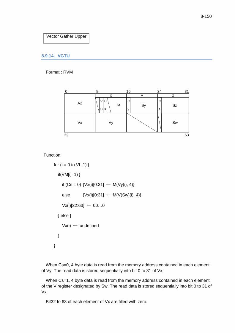
8-150
Vector Gather Upper
8.9.14. VGTU
Format : RVM
x
A2 Sy Sz
y
C
y
z
C
z
8 16 24 31
32 63
0
Vx Vy
V
C
M
C
s
Sw
Function:
for (i = 0 to VL-1) {
if(VM[i]=1) {
if (Cs = 0) {Vx(i)[0:31] ← M(Vy(i), 4)}
else {Vx(i)[0:31] ← M(V(Sw)(i), 4)}
Vx(i)[32:63] ← 00…0
} else {
Vx(i) ← undefined
}
}
When Cs=0, 4 byte data is read from the memory address contained in each element
of Vy. The read data is stored sequentially into bit 0 to 31 of Vx.
When Cs=1, 4 byte data is read from the memory address contained in each element
of the V register designated by Sw. The read data is stored sequentially into bit 0 to 31 of
Vx.
Bit32 to 63 of each element of Vx are filled with zero.
8-151
This instruction is an element-maskable vector instruction.An undefined value may be
loaded to the Vx[i] element where the corresponding VM[i]=0, and no memory-related
exception is detected for the element.
The lowest two bits of any read address must be zero, otherwise memory access
exception occurs.
Sy and Sz respectively specify the lowest and highest memory addresses to designate
the region that potentially covers accesses by this instruction. The accesses by this
instruction are assumed to be confined in the area specified by Sy and Sz. The virtual
area information is taken into consideration of memory dependency check with the
following memory access instructions (*1). If any target address (es) by this instruction
should be out of the area, the code’s semantics may not be preserved for the element(s).
If Sy is larger than Sz, it may cause an unexpected result unless Sz<4. When a value
less than four is given to Sz, the hardware preserves its memory semantics regardless of
Sy value.
Exceptions:
・Missing page exception
・Missing space exception
・Memory access exception
・Illegal data format exception : When VL > MVL
Notes:
・When Cz=0, z operand is regarded as an immediate zero irrespective of the value
of Sz.
・See also Chapter 6 for ADB functionality.
*1
LDS,LDU,LDL,LD1B,LD2B,DLDS,DLDU,DLDL,PFCH,STS,S
TU,STL,ST1B,ST2B,TS1AM,TS2AM,TS3AM,ATMAM,CAS,V
LD,VLDU,VLDL,VLD2D,VLDU2D,VLDL2D,PFCHV,VST,VSTU
,VSTL,VST2D,VSTU2D,VSTL2D,VGT,VGTU,VGTL,VSC,VSC
U,VSCL
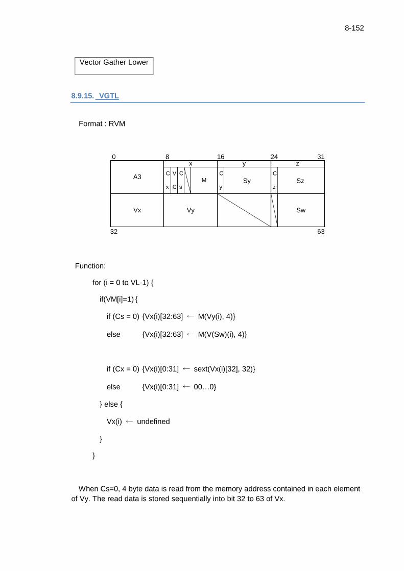
8-152
Vector Gather Lower
8.9.15. VGTL
Format : RVM
x
A3 Sy Sz
y
C
y
z
C
z
8 16 24 31
32 63
0
C
x
Vx Vy
V
C
M
C
s
Sw
Function:
for (i = 0 to VL-1) {
if(VM[i]=1) {
if (Cs = 0) {Vx(i)[32:63] ← M(Vy(i), 4)}
else {Vx(i)[32:63] ← M(V(Sw)(i), 4)}
if (Cx = 0) {Vx(i)[0:31] ← sext(Vx(i)[32], 32)}
else {Vx(i)[0:31] ← 00…0}
} else {
Vx(i) ← undefined
}
}
When Cs=0, 4 byte data is read from the memory address contained in each element
of Vy. The read data is stored sequentially into bit 32 to 63 of Vx.
8-153
When Cs=1, 4 byte data is read from the memory address contained in each element
of the V register designated by Sw. The read data is stored sequentially into bit 32 to 63
of Vx.
When Cx=0, bit0 to 31 of each element of Vx are filled with the value of the element's
bit32 for sign extension. When Cx=1, bit 0 to 31 are simply filled with all zero.
This instruction is an element-maskable vector instruction.An undefined value may be
loaded to the Vx[i] element where the corresponding VM[i]=0, and no memory-related
exception is detected for the element.
The lowest two bits of any read address must be zero, otherwise memory access
exception occurs.
Sy and Sz respectively specify the lowest and highest memory addresses to designate
the region that potentially covers accesses by this instruction. The accesses by this
instruction are assumed to be confined in the area specified by Sy and Sz. The virtual
area information is taken into consideration of memory dependency check with the
following memory access instructions (*1). If any target address (es) by this instruction
should be out of the area, the code’s semantics may not be preserved for the element(s).
If Sy is larger than Sz, it may cause an unexpected result unless Sz<4. When a value
less than four is given to Sz, the hardware preserves its memory semantics regardless of
Sy value.
Exceptions:
・Missing page exception
・Missing space exception
・Memory access exception
・Illegal data format exception : When VL > MVL
Notes:
・When Cz=0, z operand is regarded as an immediate zero irrespective of the value of Sz.
・See also Chapter 6 for ADB functionality.
*1
LDS,LDU,LDL,LD1B,LD2B,DLDS,DLDU,DLDL,PFCH,STS,S
TU,STL,ST1B,ST2B,TS1AM,TS2AM,TS3AM,ATMAM,CAS,V
LD,VLDU,VLDL,VLD2D,VLDU2D,VLDL2D,PFCHV,VST,VSTU
,VSTL,VST2D,VSTU2D,VSTL2D,VGT,VGTU,VGTL,VSC,VSC
U,VSCL
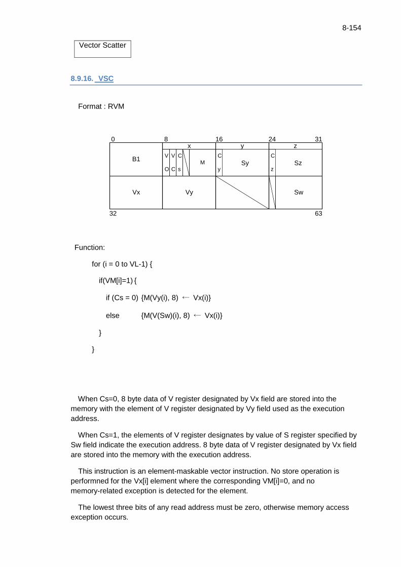
8-154
Vector Scatter
8.9.16. VSC
Format : RVM
x
B1 Sy Sz
y
C
y
z
C
z
8 16 24 31
32 63
0
Vx Vy Sw
M
V
C
C
s
V
O
Function:
for (i = 0 to VL-1) {
if(VM[i]=1) {
if (Cs = 0) {M(Vy(i), 8) ← Vx(i)}
else {M(V(Sw)(i), 8) ← Vx(i)}
}
}
When Cs=0, 8 byte data of V register designated by Vx field are stored into the
memory with the element of V register designated by Vy field used as the execution
address.
When Cs=1, the elements of V register designates by value of S register specified by
Sw field indicate the execution address. 8 byte data of V register designated by Vx field
are stored into the memory with the execution address.
This instruction is an element-maskable vector instruction. No store operation is
performned for the Vx[i] element where the corresponding VM[i]=0, and no
memory-related exception is detected for the element.
The lowest three bits of any read address must be zero, otherwise memory access
exception occurs.
8-155
Sy and Sz respectively specify the lowest and highest memory addresses to designate
the region that potentially covers accesses by this instruction. The accesses by this
instruction are assumed to be confined in the area specified by Sy and Sz. The virtual
area information is taken into consideration of memory dependency check with the
following memory access instructions (*1). If any target address (es) by this instruction
should be out of the area, the code’s semantics may not be preserved for the element(s).
If Sy is larger than Sz, it may cause an unexpected result unless Sz<4. When a value
less than four is given to Sz, the hardware preserves its memory semantics regardless of
Sy value.
When VO=0, the address dependence guarantees between VSC and the other
memory access instructions based on value of the above Sy and Sz.
When VO=1, the address dependence does not guarantee between VSC and the other
memory access instructions (*1,*2,*3) until SVOB instruction is executed. After SVOB
instruction executes, the address dependence guarantees based on value of the above
Sy and Sz.
Exceptions:
・Memory protection exception
・Missing page exception
・Missing space exception
・Memory access exception
・Illegal data format exception : When VL > MVL
Notes:
・When Cz=0, z operand is regarded as an immediate zero irrespective of the value
of Sz.
・Refer to SVOB.
*1:LDS,LDU,LDL,LD1B,LD2B,DLDS,DLDU,DLDL,PFCH,STS,STU,STL,ST1B,
ST2B,TS1AM,TS2AM,TS3AM,ATMAM,CAS,VLD,VLDU,VLD
L,VLD2D,VLDU2D,VLDL2D,PFCHV,VST,VSTU,VSTL,VST2D,
VSTU2D,VSTL2D,VGT,VGTU,VGTL,VSC,VSCU,VSCL
・*2:STS,STU,STL,ST1B,ST2B,STM
・*3:VLD,VLDU,VLDL,VLD2D,VLDU2D,VLDL2D,VGT,VGTU,VGTL,PFCHV
8-156
Vector Scatter Upper
8.9.17. VSCU
Format : RVM
x
B2 Sy Sz
y
C
y
z
C
z
8 16 24 31
32 63
0
Vx Vy
V
O
M
V
C
C
s
Sw
Function:
for (i = 0 to VL-1) {
if(VM[i]=1) {
if (Cs = 0) {M(Vy(i), 4) ← Vx(i)[0:31]}
else {M(V(Sw)(i), 4) ← Vx(i)[0:31]}
}
}
When Cs=0, bits 0 to 31 of V register designated by Vx field are stored into the
memory with the element of V register designated by Vy field used as the execution
address.
When Cs=1, the elements of V register designates by value of S register specified by
Sw field indicate the execution address. Bit 0 to 31 of V register designated by Vx field
are stored into the memory with the execution address.
This instruction is an element-maskable vector instruction. No store operation is
performned for the Vx[i] element where the corresponding VM[i]=0, and no
memory-related exception is detected for the element.
The lowest two bits of any read address must be zero, otherwise memory access
exception occurs.
8-157
Sy and Sz respectively specify the lowest and highest memory addresses to designate
the region that potentially covers accesses by this instruction. The accesses by this
instruction are assumed to be confined in the area specified by Sy and Sz. The virtual
area information is taken into consideration of memory dependency check with the
following memory access instructions (*1). If any target address (es) by this instruction
should be out of the area, the code’s semantics may not be preserved for the element(s).
If Sy is larger than Sz, it may cause an unexpected result unless Sz<4. When a value
less than four is given to Sz, the hardware preserves its memory semantics regardless of
Sy value.
When VO=0, the address dependence guarantees between VSCU and the other
memory access instructions based on value of the above Sy and Sz.
When VO=1, the address dependence does not guarantee between VSCU and the
other memory access instructions (*1,*2,*3) until SVOB instruction is executed. After
SVOB instruction executes, the address dependence guarantees based on value of the
above Sy and Sz.
Exceptions:
・Memory protection exception
・Missing page exception
・Missing space exception
・Memory access exception
・Illegal data format exception : When VL > MVL
Notes:
・When Cz=0, z operand is regarded as an immediate zero irrespective of the value
of Sz.
・Refer to SVOB.
*1:LDS,LDU,LDL,LD1B,LD2B,DLDS,DLDU,DLDL,PFCH,STS,STU,STL,ST1B,
ST2B,TS1AM,TS2AM,TS3AM,ATMAM,CAS,VLD,VLDU,VLD
L,VLD2D,VLDU2D,VLDL2D,PFCHV,VST,VSTU,VSTL,VST2D,
VSTU2D,VSTL2D,VGT,VGTU,VGTL,VSC,VSCU,VSCL
・*2:STS,STU,STL,ST1B,ST2B,STM
・*3:VLD,VLDU,VLDL,VLD2D,VLDU2D,VLDL2D,VGT,VGTU,VGTL,PFCHV

8-158
Vector Scatter Lower
8.9.18. VSCL
Format : RVM
x
B3 Sy Sz
y
C
y
z
C
z
8 16 24 31
32 63
0
Vx
M
V
C
V
O
Vy
C
s
Sw
Function:
for (i = 0 to VL-1) {
if(VM[i]=1) {
if (Cs = 0) {M(Vy(i), 4) ← Vx(i)[32:63]}
else {M(V(Sw)(i), 4) ← Vx(i)[32:63]}
}
}
When Cs=0, bit 32 to 63 of V register designated by Vx field are stored into the
memory with the element of V register designated by Vy field used as the execution
address.
When Cs=1, the elements of V register designates by value of S register specified by
Sw field indicate the execution address. Bit 32 to 63 of V register designated by Vx field
are stored into the memory with the execution address.
This instruction is an element-maskable vector instruction. No store operation is
performned for the Vx[i] element where the corresponding VM[i]=0, and no
memory-related exception is detected for the element.
The lowest two bits of any read address must be zero, otherwise memory access
exception occurs.
8-159
Sy and Sz respectively specify the lowest and highest memory addresses to designate
the region that potentially covers accesses by this instruction. The accesses by this
instruction are assumed to be confined in the area specified by Sy and Sz. The virtual
area information is taken into consideration of memory dependency check with the
following memory access instructions (*1). If any target address (es) by this instruction
should be out of the area, the code’s semantics may not be preserved for the element(s).
If Sy is larger than Sz, it may cause an unexpected result unless Sz<4. When a value
less than four is given to Sz, the hardware preserves its memory semantics regardless of
Sy value.
When VO=0, the address dependence guarantees between VSCL and the other
memory access instructions based on value of the above Sy and Sz.
When VO=1, the address dependence does not guarantee between VSCL and the
other memory access instructions (*1,*2,*3) until SVOB instruction is executed. After
SVOB instruction executes, the address dependence guarantees based on value of the
above Sy and Sz.
Exceptions:
・Memory protection exception
・Missing page exception
・Missing space exception
・Memory access exception
・Illegal data format exception : When VL > MVL
Notes:
・When Cz=0, z operand is regarded as an immediate zero irrespective of the value of
Sz.
・Refer to SVOB.
*1:LDS,LDU,LDL,LD1B,LD2B,DLDS,DLDU,DLDL,PFCH,STS,STU,STL,ST1B,
ST2B,TS1AM,TS2AM,TS3AM,ATMAM,CAS,VLD,VLDU,VLD
L,VLD2D,VLDU2D,VLDL2D,PFCHV,VST,VSTU,VSTL,VST2D,
VSTU2D,VSTL2D,VGT,VGTU,VGTL,VSC,VSCU,VSCL
・*2:STS,STU,STL,ST1B,ST2B,STM
・*3:VLD,VLDU,VLDL,VLD2D,VLDU2D,VLDL2D,VGT,VGTU,VGTL,PFCHV
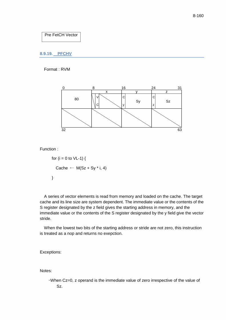
8-160
Pre FetCH Vector
8.9.19. PFCHV
Format : RVM
x
80 Sy Sz
y
C
y
z
C
z
8 16 24 31
32 63
0
V
C
Function :
for (i = 0 to VL-1) {
Cache ← M(Sz + Sy * i, 4)
}
A series of vector elements is read from memory and loaded on the cache. The target
cache and its line size are system dependent. The immediate value or the contents of the
S register designated by the z field gives the starting address in memory, and the
immediate value or the contents of the S register designated by the y field give the vector
stride.
When the lowest two bits of the starting address or stride are not zero, this instruction
is treated as a nop and returns no exepction.
Exceptions:
Notes:
・When Cz=0, z operand is the immediate value of zero irrespective of the value of
Sz.

8-161
・The cache line size of ADB is 128 bytes in Aurora.
・Refer to an item of ADB of Chapter 6 about a use presence of ADB.
・When this instruction try to access the page or the space of access prohibition,
the exception does not occur and the prefetch to the address does not operate.
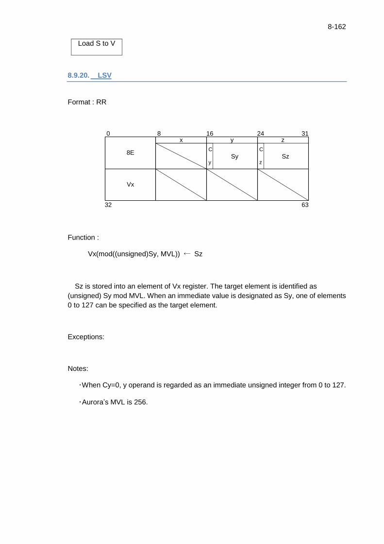
8-162
Load S to V
8.9.20. LSV
Format : RR
x
8E Sy
y
C
y
z8 16 24 31
32 63
0
Vx
SzC
z
Function :
Vx(mod((unsigned)Sy, MVL)) ← Sz
Sz is stored into an element of Vx register. The target element is identified as
(unsigned) Sy mod MVL. When an immediate value is designated as Sy, one of elements
0 to 127 can be specified as the target element.
Exceptions:
Notes:
・When Cy=0, y operand is regarded as an immediate unsigned integer from 0 to 127.
・Aurora’s MVL is 256.
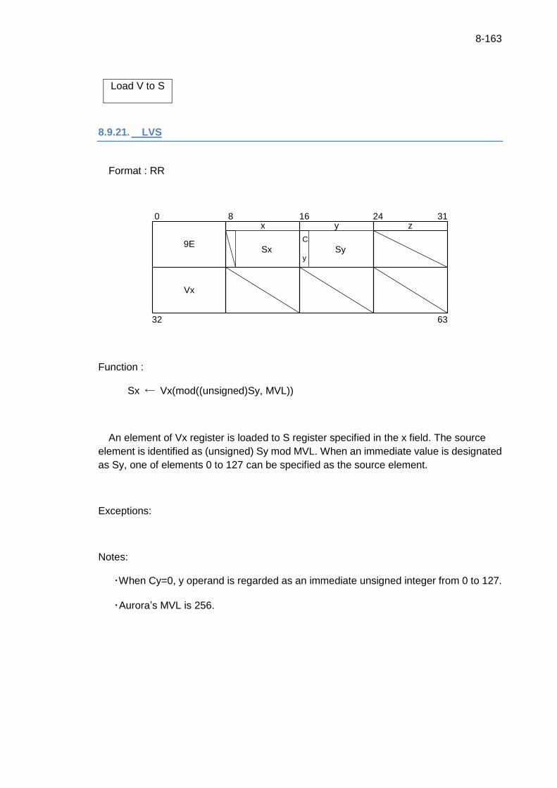
8-163
Load V to S
8.9.21. LVS
Format : RR
x
9E Sy
y
C
y
z8 16 24 31
32 63
0
Vx
Sx
Function :
Sx ← Vx(mod((unsigned)Sy, MVL))
An element of Vx register is loaded to S register specified in the x field. The source
element is identified as (unsigned) Sy mod MVL. When an immediate value is designated
as Sy, one of elements 0 to 127 can be specified as the source element.
Exceptions:
Notes:
・When Cy=0, y operand is regarded as an immediate unsigned integer from 0 to 127.
・Aurora’s MVL is 256.
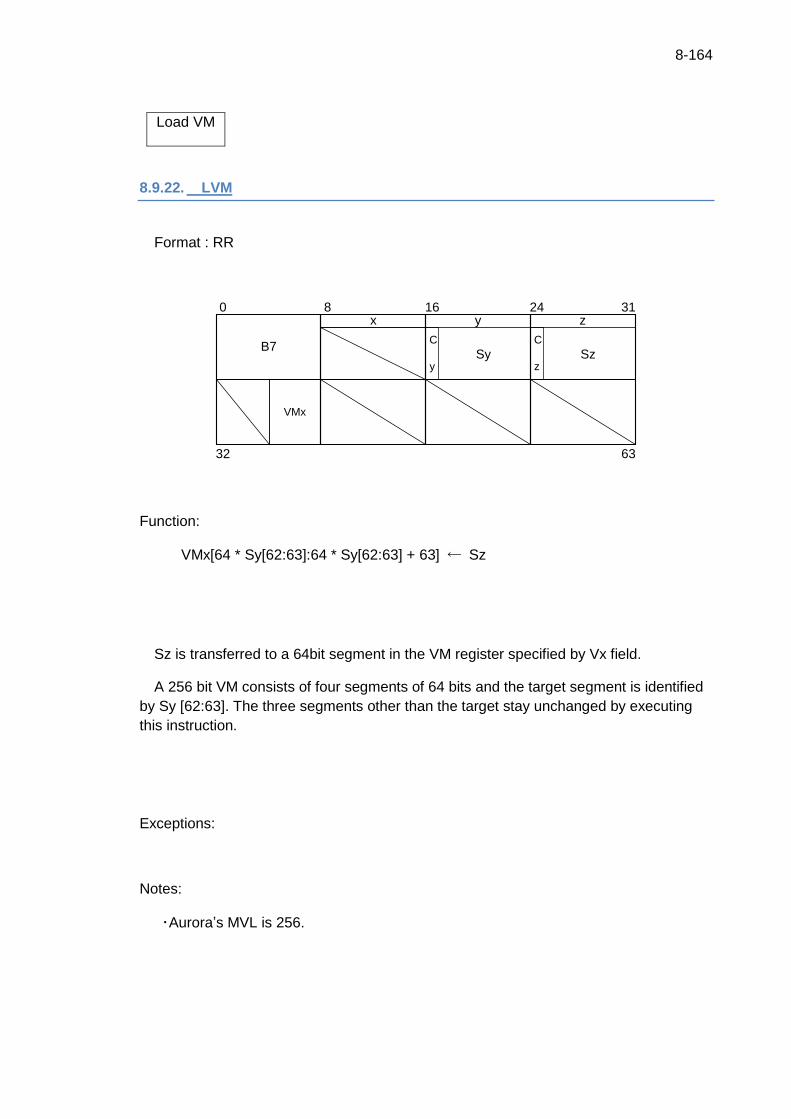
8-164
Load VM
8.9.22. LVM
Format : RR
x
B7 Sy
y
C
y
z8 16 24 31
32 63
0
VMx
SzC
z
Function:
VMx[64 * Sy[62:63]:64 * Sy[62:63] + 63] ← Sz
Sz is transferred to a 64bit segment in the VM register specified by Vx field.
A 256 bit VM consists of four segments of 64 bits and the target segment is identified
by Sy [62:63]. The three segments other than the target stay unchanged by executing
this instruction.
Exceptions:
Notes:
・Aurora’s MVL is 256.
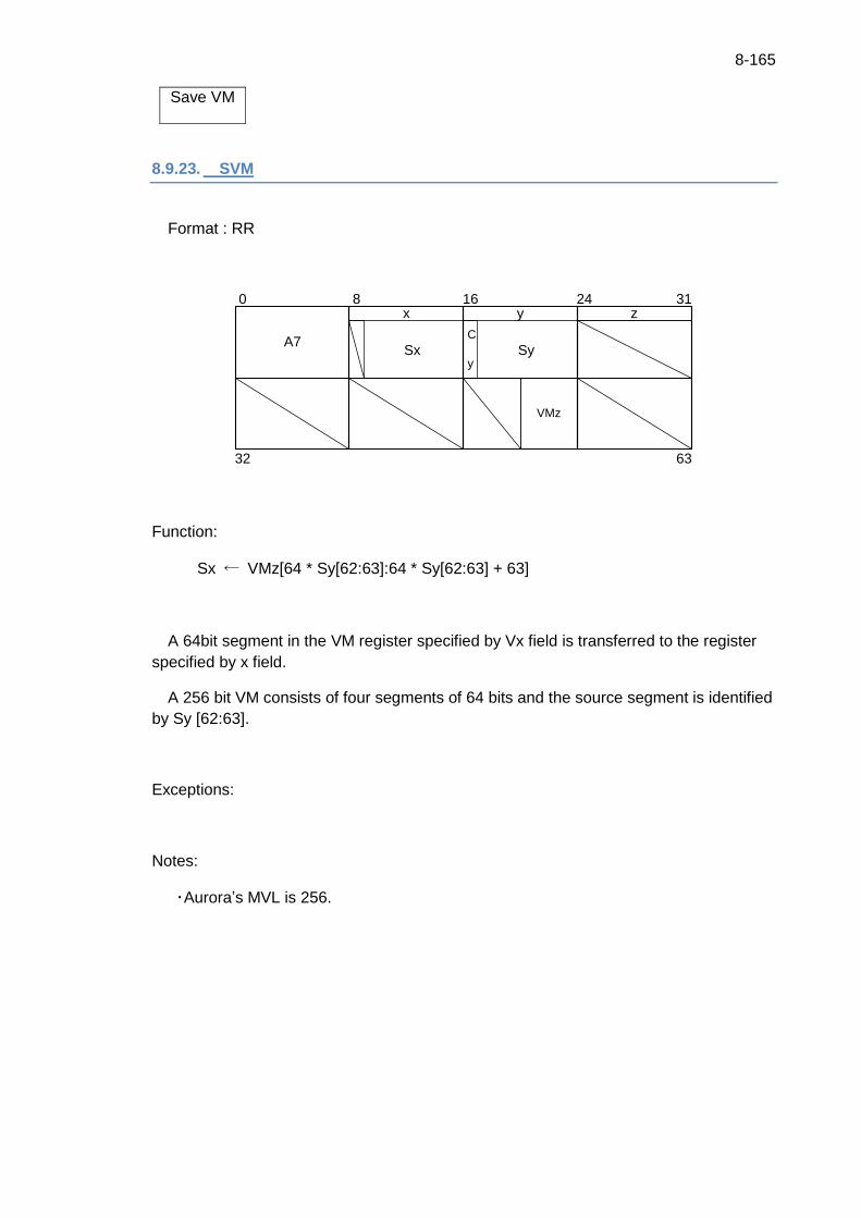
8-165
Save VM
8.9.23. SVM
Format : RR
x
A7
z8 16 24 31
32 63
0
Sx
VMz
Sy
y
C
y
Function:
Sx ← VMz[64 * Sy[62:63]:64 * Sy[62:63] + 63]
A 64bit segment in the VM register specified by Vx field is transferred to the register
specified by x field.
A 256 bit VM consists of four segments of 64 bits and the source segment is identified
by Sy [62:63].
Exceptions:
Notes:
・Aurora’s MVL is 256.
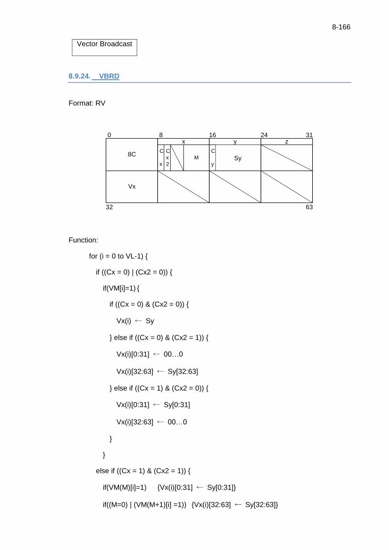
8-166
Vector Broadcast
8.9.24. VBRD
Format: RV
x
8C Sy
y
C
y
z8 16 24 31
32 63
0
Vx
M
C
x
2
C
x
Function:
for (i = 0 to VL-1) {
if ((Cx = 0) | (Cx2 = 0)) {
if(VM[i]=1) {
if ((Cx = 0) & (Cx2 = 0)) {
Vx(i) ← Sy
} else if ((Cx = 0) & (Cx2 = 1)) {
Vx(i)[0:31] ← 00…0
Vx(i)[32:63] ← Sy[32:63]
} else if ((Cx = 1) & (Cx2 = 0)) {
Vx(i)[0:31] ← Sy[0:31]
Vx(i)[32:63] ← 00…0
}
}
else if ((Cx = 1) & (Cx2 = 1)) {
if(VM(M)[i]=1) {Vx(i)[0:31] ← Sy[0:31]}
if((M=0) | (VM(M+1)[i] =1)) {Vx(i)[32:63] ← Sy[32:63]}
8-167
}
}
Sy is broadcasted to each element of the V register designated by Vx field according to
Cx and Cx2 fields. This instruction is an element-maskable vector instruction.
When Cx=Cx2=0, 64bit data Sy is broadcasted to each element of Vx elements 0 –
VL-1, where its corresponding bit in the VM(M) is 1. When M=0, all mask bits are
regarded as 1.
When Cx=0 and Cx2=1, Sy [32:63] are broadcasted to bits 32 to 63 in each element of
Vx elements 0 – VL-1, where its corresponding bit in the VM(M) is 1. Upper 32bits are
filled with zeros. When M=0, all mask bits are regarded as 1.
When Cx=1 and Cx2=0, Sy [0:31] are broadcasted to bits 0 to 31 in each element of Vx
elements 0 – VL-1, where its corresponding bit in the VM(M) is 1. Lower 32bits are filled
with zeros. When M=0, all mask bits are regarded as 1.
When Cx=Cx2=1, Sy [0:31] and Sy [32:63] are broadcasted to bits 0 to 31 and bits 32 to
63 of each element of Vx elements 0-VL-1. Two VM(M) and VM(M+1) are separately
used as masks for those two 32bit vectors. When M=0, only VM(0) is used for both of
upper and lower parts. In this case, M must be an even number. Otherwise an illegal
instruction format exception occurs.
Exceptions:
・Illegal instruction format exception
・Illegal data format exception : When VL > MVL
Notes:
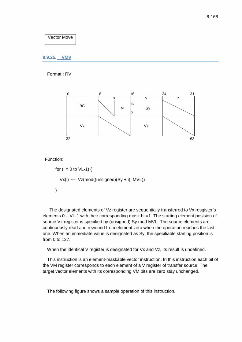
8-168
Vector Move
8.9.25. VMV
Format : RV
x
9C Sy
y
C
y
z8 16 24 31
32 63
0
Vx Vz
M
Function:
for (i = 0 to VL-1) {
Vx(i) ← Vz(mod((unsigned)(Sy + i), MVL))
}
The designated elements of Vz register are sequentially transferred to Vx resgister’s
elements 0 – VL-1 with their corresponding mask bit=1. The starting element posision of
source Vz register is specified by (unsigned) Sy mod MVL. The source elements are
continuously read and rewound from element zero when the operation reaches the last
one. When an immediate value is designated as Sy, the specifiable starting position is
from 0 to 127.
When the identical V register is designated for Vx and Vz, its result is undefined.
This instruction is an element-maskable vector instruction. In this instruction each bit of
the VM register corresponds to each element of a V register of transfer source. The
target vector elements with its corresponding VM bits are zero stay unchanged.
The following figure shows a sample operation of this instruction.
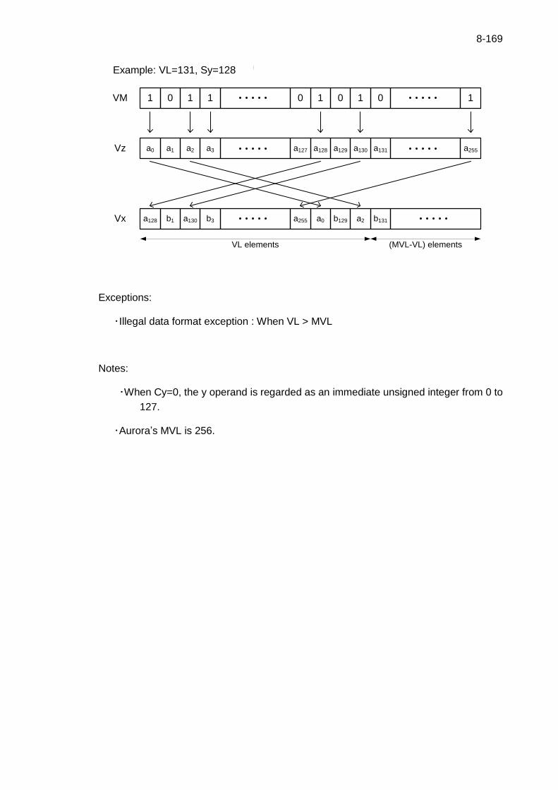
8-169
a0Vz a1 a2 a3 a127 a128 a129
1 0 1 1 1 0 1 1
a128 b1 a130 b3
VM
Vx
a130
0
a255
a0 b129 a2 b131a255
Example case: Sy=128, VL=130
a131
0
VL elements (MVL-VL) elements
Exceptions:
・Illegal data format exception : When VL > MVL
Notes:
・When Cy=0, the y operand is regarded as an immediate unsigned integer from 0 to
127.
・Aurora’s MVL is 256.
Example: VL=131, Sy=128
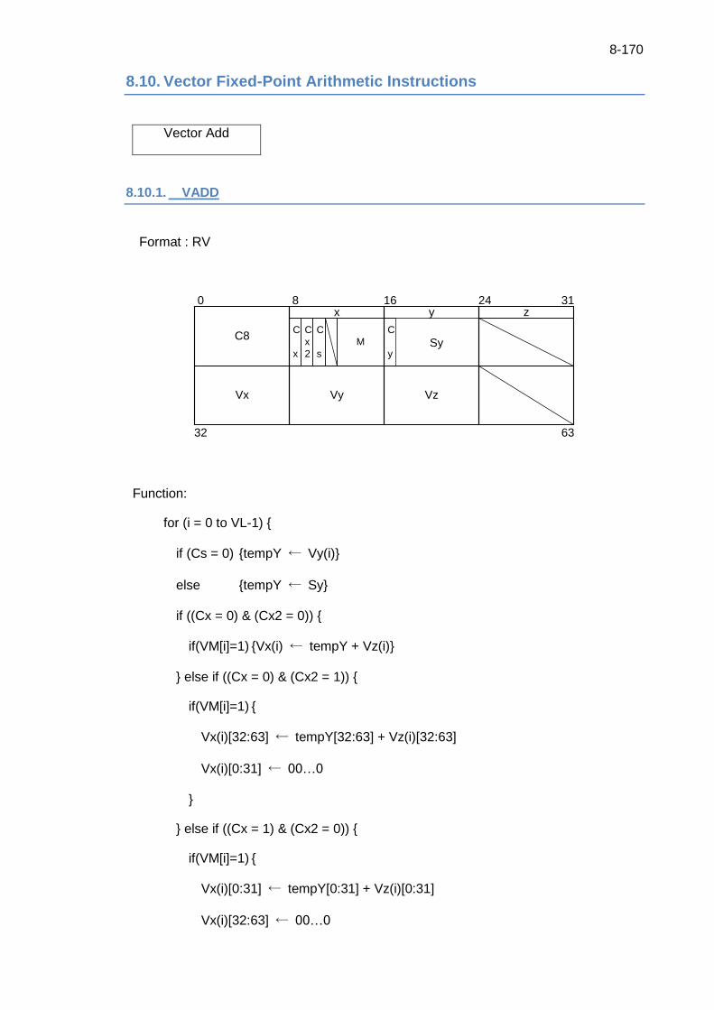
8-170
8.10. Vector Fixed-Point Arithmetic Instructions
Vector Add
8.10.1. VADD
Format : RV
x
C8 Sy
y
C
y
z8 16 24 31
32 63
0
Vx Vy Vz
M
C
s
C
x
C
x
2
Function:
for (i = 0 to VL-1) {
if (Cs = 0) {tempY ← Vy(i)}
else {tempY ← Sy}
if ((Cx = 0) & (Cx2 = 0)) {
if(VM[i]=1) {Vx(i) ← tempY + Vz(i)}
} else if ((Cx = 0) & (Cx2 = 1)) {
if(VM[i]=1) {
Vx(i)[32:63] ← tempY[32:63] + Vz(i)[32:63]
Vx(i)[0:31] ← 00…0
}
} else if ((Cx = 1) & (Cx2 = 0)) {
if(VM[i]=1) {
Vx(i)[0:31] ← tempY[0:31] + Vz(i)[0:31]
Vx(i)[32:63] ← 00…0
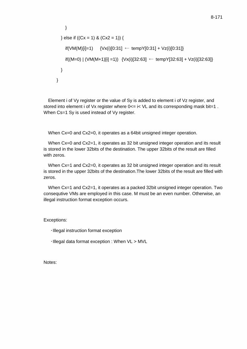
8-171
}
} else if ((Cx = 1) & (Cx2 = 1)) {
if(VM(M)[i]=1) {Vx(i)[0:31] ← tempY[0:31] + Vz(i)[0:31]}
if((M=0) | (VM(M+1)[i] =1)) {Vx(i)[32:63] ← tempY[32:63] + Vz(i)[32:63]}
}
}
Element i of Vy register or the value of Sy is added to element i of Vz register, and
stored into element i of Vx register where 0<= i< VL and its corresponding mask bit=1 .
When Cs=1 Sy is used instead of Vy register.
When Cx=0 and Cx2=0, it operates as a 64bit unsigned integer operation.
When Cx=0 and Cx2=1, it operates as 32 bit unsigned integer operation and its result
is stored in the lower 32bits of the destination. The upper 32bits of the result are filled
with zeros.
When Cx=1 and Cx2=0, it operates as 32 bit unsigned integer operation and its result
is stored in the upper 32bits of the destination.The lower 32bits of the result are filled with
zeros.
When Cx=1 and Cx2=1, it operates as a packed 32bit unsigned integer operation. Two
consequtive VMs are employed in this case. M must be an even number. Otherwise, an
illegal instruction format exception occurs.
Exceptions:
・Illegal instruction format exception
・Illegal data format exception : When VL > MVL
Notes:
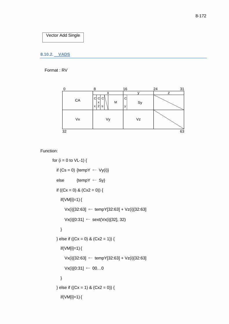
8-172
Vector Add Single
8.10.2. VADS
Format : RV
C
x
x
CA Sy
y
C
y
z8 16 24 31
32 63
0
Vx Vy Vz
M
C
s
C
x
2
Function:
for (i = 0 to VL-1) {
if (Cs = 0) {tempY ← Vy(i)}
else {tempY ← Sy}
if ((Cx = 0) & (Cx2 = 0)) {
if(VM[i]=1) {
Vx(i)[32:63] ← tempY[32:63] + Vz(i)[32:63]
Vx(i)[0:31] ← sext(Vx(i)[32], 32)
}
} else if ((Cx = 0) & (Cx2 = 1)) {
if(VM[i]=1) {
Vx(i)[32:63] ← tempY[32:63] + Vz(i)[32:63]
Vx(i)[0:31] ← 00…0
}
} else if ((Cx = 1) & (Cx2 = 0)) {
if(VM[i]=1) {
8-173
Vx(i)[0:31] ← tempY[0:31] + Vz(i)[0:31]
Vx(i)[32:63] ← 00…0
}
} else if ((Cx = 1) & (Cx2 = 1)) {
if(VM(M)[i]=1) {Vx(i)[0:31] ← tempY[0:31] + Vz(i)[0:31]}
if((M=0) | (VM(M+1)[i] =1)) {Vx(i)[32:63] ← tempY[32:63] + Vz(i)[32:63]}
}
}
Element i of Vy register or the value of Sy is added to element i of Vz register, and
stored into element i of Vx register where 0<= i< VL and its corresponding mask bit=1 .
When Cs=1 Sy is used instead of Vy register. Depending on the result a fixed-point
overflow exception can be detected.
When Cx=0 and Cx2=0, it operates as a 32-bit signed integer operation. The upper
32-bits of the result are filled with extended sign bits.
When Cx=0 and Cx2=1, it operates as 32 bit signed integer operation and its result is
stored in the lower 32bits of the destination. The upper 32bits of the result are filled with
zeros.
When Cx=1 and Cx2=0, it operates as 32 bit signed integer operation and its result is
stored in the upper 32bits of the destination.The lower 32bits of the result are filled with
zeros.
When Cx=1 and Cx2=1, it operates as a packed 32-bit signed integer operation. Two
VMs are employed in this case. M must be an even number. Otherwise, an illegal
instruction format exception is generated.
This instruction is an element-maskable vector instruction.
Exceptions:
・Illegal instruction format exception
・Fixed-point overflow exception
・Illegal data format exception : When VL > MVL
8-174
Vector Add
8.10.3. VADX
Format : RV
x
8B Sy
y
C
y
z8 16 24 31
32 63
0
Vx Vy Vz
M
C
s
Function:
for (i = 0 to VL-1) {
if (Cs = 0) {tempY ← Vy(i)}
else {tempY ← Sy}
if(VM[i]=1) {Vx(i) ← tempY + Vz(i)}
}
Element i of Vy register or the value of Sy is added to element i of Vz register, and
stored into element i of Vx register where 0<= i< VL and its corresponding mask bit=1 .
When Cs=1 Sy is used instead of Vy register. Depending on the result a fixed-point
overflow exception can be detected.
It operates as a 64-bit signed integer operation.
This instruction is an element-maskable vector instruction.
Exceptions:
・Fixed-point overflow exception
・Illegal data format exception : When VL > MVL
8-175
Vector Subtract
8.10.4. VSUB
Format : RV
x
D8 Sy
y
C
y
z8 16 24 31
32 63
0
Vx Vy Vz
M
C
s
C
x
C
x
2
Function:
for (i = 0 to VL-1) {
if (Cs = 0) {tempY ← Vy(i)}
else {tempY ← Sy}
if ((Cx = 0) & (Cx2 = 0)) {
if(VM[i]=1) {Vx(i) ← tempY - Vz(i)}
} else if ((Cx = 0) & (Cx2 = 1)) {
if(VM[i]=1) {
Vx(i)[32:63] ← tempY[32:63] - Vz(i)[32:63]
Vx(i)[0:31] ← 00…0
}
} else if ((Cx = 1) & (Cx2 = 0)) {
if(VM[i]=1) {
Vx(i)[0:31] ← tempY[0:31] - Vz(i)[0:31]
Vx(i)[32:63] ← 00…0
}
8-176
} else if ((Cx = 1) & (Cx2 = 1)) {
if(VM(M)[i]=1) {Vx(i)[0:31] ← tempY[0:31] - Vz(i)[0:31]}
if((M=0) | (VM(M+1)[i] =1)) {Vx(i)[32:63] ← tempY[32:63] - Vz(i)[32:63]}
}
}
Element i of Vz register is subtracted from element i of Vy register or the value of Sy,
and stored into element i of Vx register where 0<= i< VL and its corresponding mask
bit=1 . When Cs=1 Sy is used instead of Vy register.
When Cx=0 and Cx2=0, it operates as a 64-bit unsigned integer operation.
When Cx=0 and Cx2=1, it operates as 32 bit unsigned integer operation and its result
is stored in the lower 32bits of the destination. The upper 32bits of the result are filled
with zeros.
When Cx=1 and Cx2=0, it operates as 32 bit unsigned integer operation and its result
is stored in the upper 32bits of the destination.The lower 32bits of the result are filled with
zeros.
When Cx=1 and Cx2=1, it operates as a packed 32-bit unsigned integer operation.
Two consequtive VMs are employed in this case. M must be an even number. Otherwise
an illegal instruction format exception is generated.
This instruction is an element-maskable vector instruction.
Exceptions:
・Illegal instruction format exception
・Illegal data format exception : When VL > MVL
Notes:
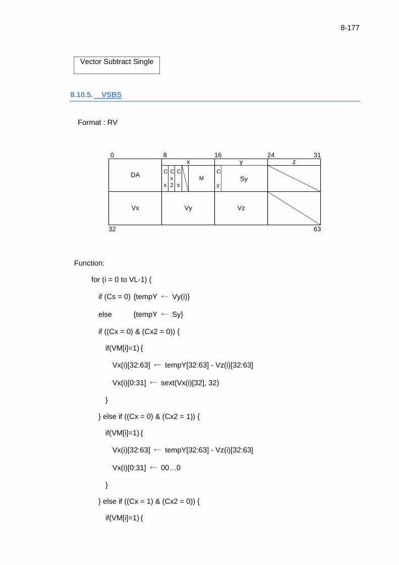
8-177
Vector Subtract Single
8.10.5. VSBS
Format : RV
x
DA Sy
y
C
y
z8 16 24 31
32 63
0
Vx Vy Vz
C
x
M
C
s
C
x
2
Function:
for (i = 0 to VL-1) {
if (Cs = 0) {tempY ← Vy(i)}
else {tempY ← Sy}
if ((Cx = 0) & (Cx2 = 0)) {
if(VM[i]=1) {
Vx(i)[32:63] ← tempY[32:63] - Vz(i)[32:63]
Vx(i)[0:31] ← sext(Vx(i)[32], 32)
}
} else if ((Cx = 0) & (Cx2 = 1)) {
if(VM[i]=1) {
Vx(i)[32:63] ← tempY[32:63] - Vz(i)[32:63]
Vx(i)[0:31] ← 00…0
}
} else if ((Cx = 1) & (Cx2 = 0)) {
if(VM[i]=1) {
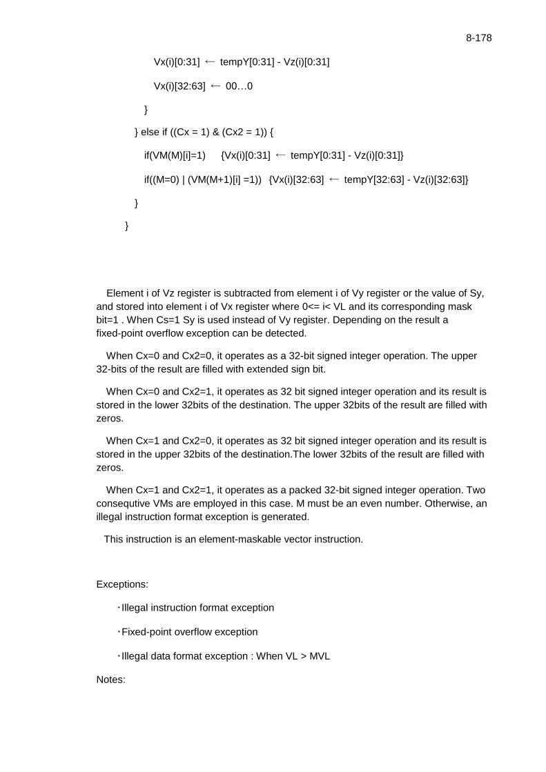
8-178
Vx(i)[0:31] ← tempY[0:31] - Vz(i)[0:31]
Vx(i)[32:63] ← 00…0
}
} else if ((Cx = 1) & (Cx2 = 1)) {
if(VM(M)[i]=1) {Vx(i)[0:31] ← tempY[0:31] - Vz(i)[0:31]}
if((M=0) | (VM(M+1)[i] =1)) {Vx(i)[32:63] ← tempY[32:63] - Vz(i)[32:63]}
}
}
Element i of Vz register is subtracted from element i of Vy register or the value of Sy,
and stored into element i of Vx register where 0<= i< VL and its corresponding mask
bit=1 . When Cs=1 Sy is used instead of Vy register. Depending on the result a
fixed-point overflow exception can be detected.
When Cx=0 and Cx2=0, it operates as a 32-bit signed integer operation. The upper
32-bits of the result are filled with extended sign bit.
When Cx=0 and Cx2=1, it operates as 32 bit signed integer operation and its result is
stored in the lower 32bits of the destination. The upper 32bits of the result are filled with
zeros.
When Cx=1 and Cx2=0, it operates as 32 bit signed integer operation and its result is
stored in the upper 32bits of the destination.The lower 32bits of the result are filled with
zeros.
When Cx=1 and Cx2=1, it operates as a packed 32-bit signed integer operation. Two
consequtive VMs are employed in this case. M must be an even number. Otherwise, an
illegal instruction format exception is generated.
This instruction is an element-maskable vector instruction.
Exceptions:
・Illegal instruction format exception
・Fixed-point overflow exception
・Illegal data format exception : When VL > MVL
Notes:
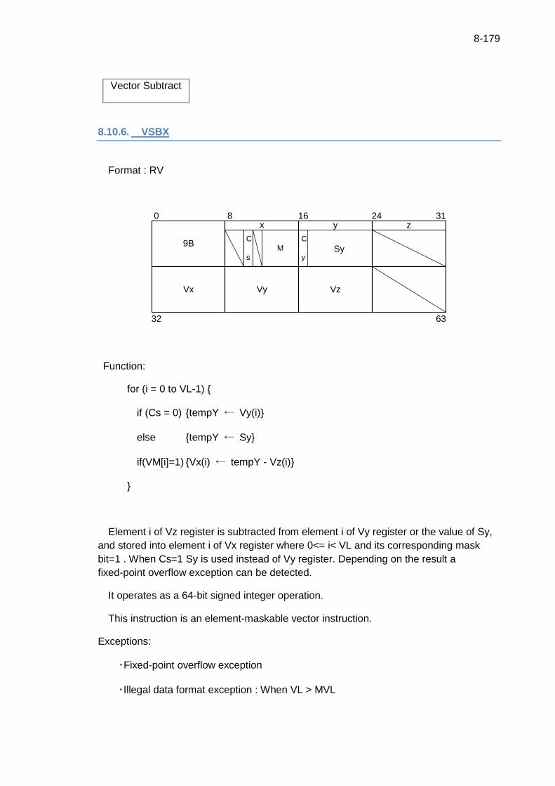
8-179
Vector Subtract
8.10.6. VSBX
Format : RV
x
9B Sy
y
C
y
z8 16 24 31
32 63
0
Vx Vy Vz
M
C
s
Function:
for (i = 0 to VL-1) {
if (Cs = 0) {tempY ← Vy(i)}
else {tempY ← Sy}
if(VM[i]=1) {Vx(i) ← tempY - Vz(i)}
}
Element i of Vz register is subtracted from element i of Vy register or the value of Sy,
and stored into element i of Vx register where 0<= i< VL and its corresponding mask
bit=1 . When Cs=1 Sy is used instead of Vy register. Depending on the result a
fixed-point overflow exception can be detected.
It operates as a 64-bit signed integer operation.
This instruction is an element-maskable vector instruction.
Exceptions:
・Fixed-point overflow exception
・Illegal data format exception : When VL > MVL
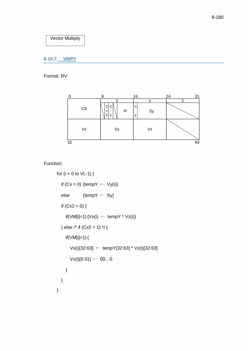
8-180
Vector Multiply
8.10.7. VMPY
Format: RV
x
C9 Sy
y
C
y
z8 16 24 31
32 63
0
Vx Vy Vz
M
C
s
C
x
2
Function:
for (i = 0 to VL-1) {
if (Cs = 0) {tempY ← Vy(i)}
else {tempY ← Sy}
if (Cx2 = 0) {
if(VM[i]=1) {Vx(i) ← tempY * Vz(i)}
} else /* if (Cx2 = 1) */ {
if(VM[i]=1) {
Vx(i)[32:63] ← tempY[32:63] * Vz(i)[32:63]
Vx(i)[0:31] ← 00…0
}
}
}
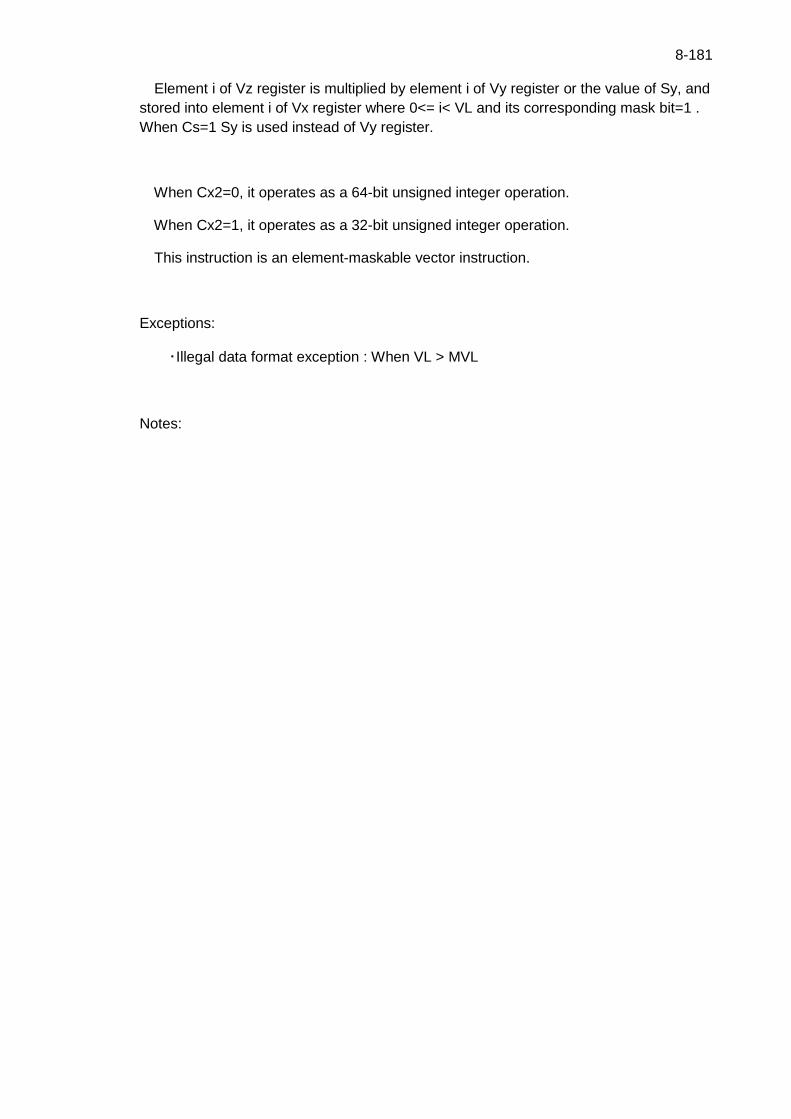
8-181
Element i of Vz register is multiplied by element i of Vy register or the value of Sy, and
stored into element i of Vx register where 0<= i< VL and its corresponding mask bit=1 .
When Cs=1 Sy is used instead of Vy register.
When Cx2=0, it operates as a 64-bit unsigned integer operation.
When Cx2=1, it operates as a 32-bit unsigned integer operation.
This instruction is an element-maskable vector instruction.
Exceptions:
・Illegal data format exception : When VL > MVL
Notes:
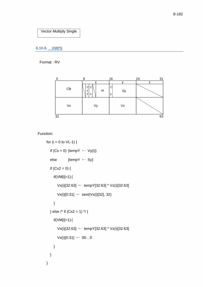
8-182
Vector Multiply Single
8.10.8. VMPS
Format : RV
x
CB Sy
y
C
y
z8 16 24 31
32 63
0
Vx Vy Vz
M
C
s
C
x
2
Function:
for (i = 0 to VL-1) {
if (Cs = 0) {tempY ← Vy(i)}
else {tempY ← Sy}
if (Cx2 = 0) {
if(VM[i]=1) {
Vx(i)[32:63] ← tempY[32:63] * Vz(i)[32:63]
Vx(i)[0:31] ← sext(Vx(i)[32], 32)
}
} else /* if (Cx2 = 1) */ {
if(VM[i]=1) {
Vx(i)[32:63] ← tempY[32:63] * Vz(i)[32:63]
Vx(i)[0:31] ← 00…0
}
}
}
8-183
Element i of Vz register is multiplied by element i of Vy register or the value of Sy, and
stored into element i of Vx register where 0<= i< VL and its corresponding mask bit=1 .
When Cs=1 Sy is used instead of Vy register. Depending on the result it can detect
fixed-point overflow exception.
It operates as a 32-bit signed integer operation.
When Cx2=0, the upper 32-bits of the result are filled with extended sign bit.
When Cx2=1, the upper 32-bits of the result are filled with zero.
This instruction is an element-maskable vector instruction.
Exceptions:
・Fixed-point overflow exception
・Illegal data format exception : When VL > MVL
Notes:
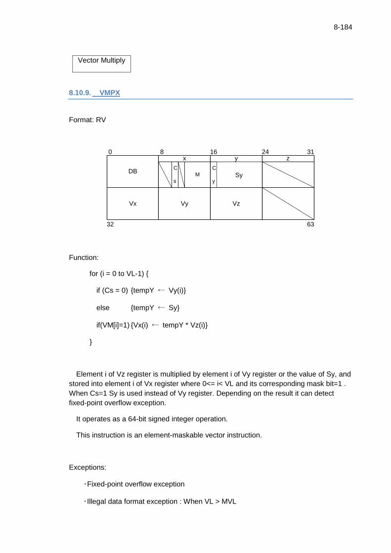
8-184
Vector Multiply
8.10.9. VMPX
Format: RV
x
DB Sy
y
C
y
z8 16 24 31
32 63
0
Vx Vy Vz
M
C
s
Function:
for (i = 0 to VL-1) {
if (Cs = 0) {tempY ← Vy(i)}
else {tempY ← Sy}
if(VM[i]=1) {Vx(i) ← tempY * Vz(i)}
}
Element i of Vz register is multiplied by element i of Vy register or the value of Sy, and
stored into element i of Vx register where 0<= i< VL and its corresponding mask bit=1 .
When Cs=1 Sy is used instead of Vy register. Depending on the result it can detect
fixed-point overflow exception.
It operates as a 64-bit signed integer operation.
This instruction is an element-maskable vector instruction.
Exceptions:
・Fixed-point overflow exception
・Illegal data format exception : When VL > MVL
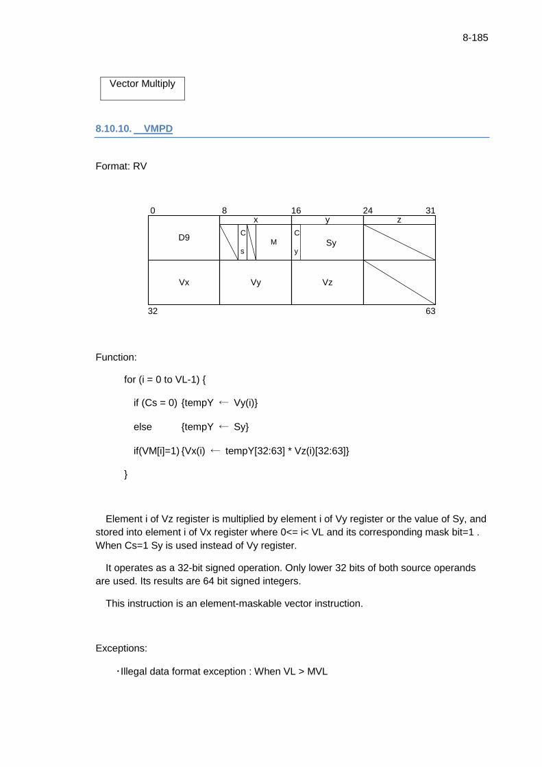
8-185
Vector Multiply
8.10.10. VMPD
Format: RV
x
D9 Sy
y
C
y
z8 16 24 31
32 63
0
Vx Vy Vz
M
C
s
Function:
for (i = 0 to VL-1) {
if (Cs = 0) {tempY ← Vy(i)}
else {tempY ← Sy}
if(VM[i]=1) {Vx(i) ← tempY[32:63] * Vz(i)[32:63]}
}
Element i of Vz register is multiplied by element i of Vy register or the value of Sy, and
stored into element i of Vx register where 0<= i< VL and its corresponding mask bit=1 .
When Cs=1 Sy is used instead of Vy register.
It operates as a 32-bit signed operation. Only lower 32 bits of both source operands
are used. Its results are 64 bit signed integers.
This instruction is an element-maskable vector instruction.
Exceptions:
・Illegal data format exception : When VL > MVL
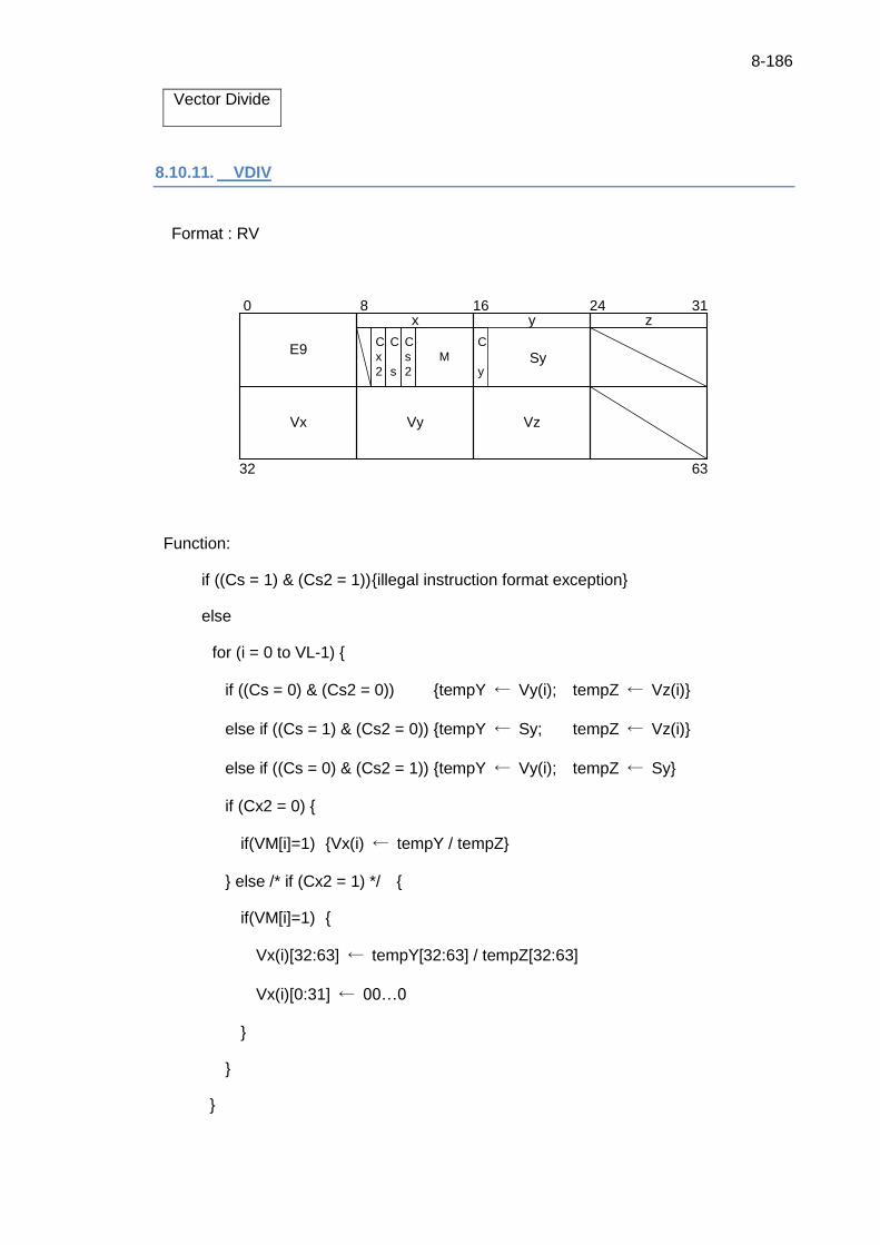
8-186
Vector Divide
8.10.11. VDIV
Format : RV
x
E9 Sy
y
C
y
z8 16 24 31
32 63
0
Vx Vy Vz
M
C
s
C
s
2
C
x
2
Function:
if ((Cs = 1) & (Cs2 = 1)) {illegal instruction format exception}
else
for (i = 0 to VL-1) {
if ((Cs = 0) & (Cs2 = 0)) {tempY ← Vy(i); tempZ ← Vz(i)}
else if ((Cs = 1) & (Cs2 = 0)) {tempY ← Sy; tempZ ← Vz(i)}
else if ((Cs = 0) & (Cs2 = 1)) {tempY ← Vy(i); tempZ ← Sy}
if (Cx2 = 0) {
if(VM[i]=1) {Vx(i) ← tempY / tempZ}
} else /* if (Cx2 = 1) */ {
if(VM[i]=1) {
Vx(i)[32:63] ← tempY[32:63] / tempZ[32:63]
Vx(i)[0:31] ← 00…0
}
}
}
8-187
The contents of V register designated by Vz field, or the contents of the S register or
the immediate value designated by Sy field are divided by the contents of V register
designated by Vy field, or the contents of the S register or the immediate value
designated by Sy field. The results are stored into the V register designated by Vx field.
The use of S register or immediate value is specified by Cs and Cs2 field.
Two operands of element i of Vz register, element i of Vy register and the value of Sy,
are used for devision, where 0<= i< VL and its corresponding mask bit=1. Which two of
the three operands are used follows this rule.
When Cs=0 and Cs2=0, it returns Vy / Vz.
When Cs=1 and Cs2=0, it returns Sy / Vz.
When Cs=0 and Cs2=1, it returns Vy / Sy.
When Cs=1 and Cs2=1, illegal instruction format exception occurs.
Cx2 field switches this operation’s data size.
When Cx2=0, it operates as a 64-bit unsigned integer operation.
When Cx2=1, it operates as a 32-bit unsigned integer operation.
This instruction is an element-maskable vector instruction.
When its divisor is zero, division exception is detected.
Exceptions:
・Illegal instruction format exception
・Division exception
・Illegal data format exception : When VL > MVL
Notes:
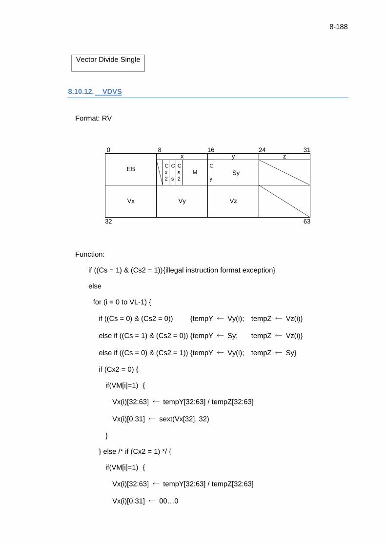
8-188
Vector Divide Single
8.10.12. VDVS
Format: RV
x
EB Sy
y
C
y
z8 16 24 31
32 63
0
Vx Vy Vz
M
C
s
C
s
2
C
x
2
Function:
if ((Cs = 1) & (Cs2 = 1)) {illegal instruction format exception}
else
for (i = 0 to VL-1) {
if ((Cs = 0) & (Cs2 = 0)) {tempY ← Vy(i); tempZ ← Vz(i)}
else if ((Cs = 1) & (Cs2 = 0)) {tempY ← Sy; tempZ ← Vz(i)}
else if ((Cs = 0) & (Cs2 = 1)) {tempY ← Vy(i); tempZ ← Sy}
if (Cx2 = 0) {
if(VM[i]=1) {
Vx(i)[32:63] ← tempY[32:63] / tempZ[32:63]
Vx(i)[0:31] ← sext(Vx[32], 32)
}
} else /* if (Cx2 = 1) */ {
if(VM[i]=1) {
Vx(i)[32:63] ← tempY[32:63] / tempZ[32:63]
Vx(i)[0:31] ← 00…0
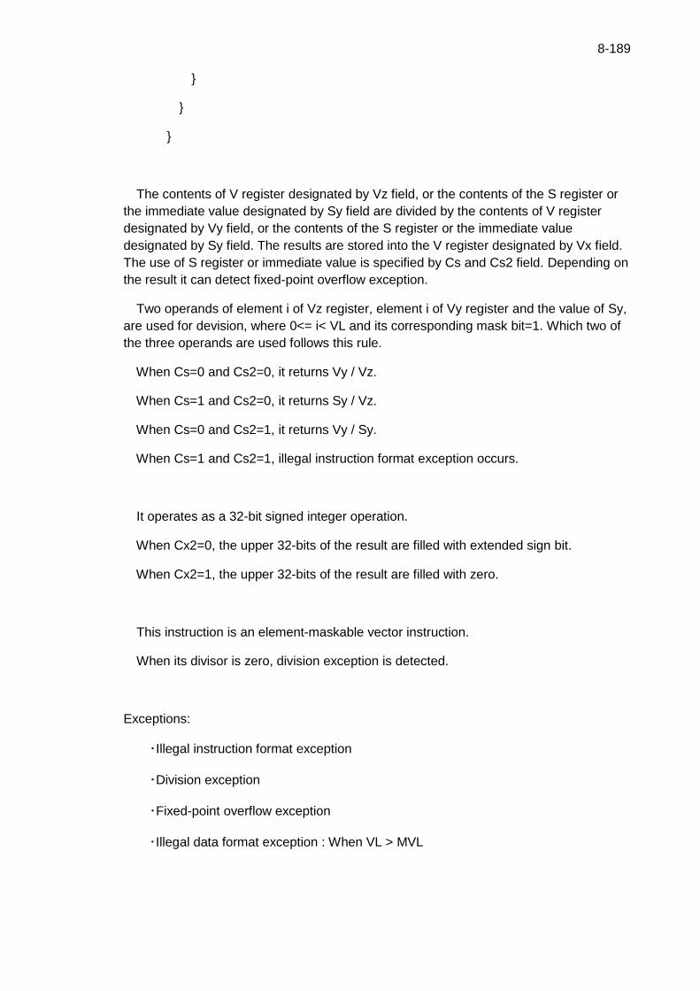
8-189
}
}
}
The contents of V register designated by Vz field, or the contents of the S register or
the immediate value designated by Sy field are divided by the contents of V register
designated by Vy field, or the contents of the S register or the immediate value
designated by Sy field. The results are stored into the V register designated by Vx field.
The use of S register or immediate value is specified by Cs and Cs2 field. Depending on
the result it can detect fixed-point overflow exception.
Two operands of element i of Vz register, element i of Vy register and the value of Sy,
are used for devision, where 0<= i< VL and its corresponding mask bit=1. Which two of
the three operands are used follows this rule.
When Cs=0 and Cs2=0, it returns Vy / Vz.
When Cs=1 and Cs2=0, it returns Sy / Vz.
When Cs=0 and Cs2=1, it returns Vy / Sy.
When Cs=1 and Cs2=1, illegal instruction format exception occurs.
It operates as a 32-bit signed integer operation.
When Cx2=0, the upper 32-bits of the result are filled with extended sign bit.
When Cx2=1, the upper 32-bits of the result are filled with zero.
This instruction is an element-maskable vector instruction.
When its divisor is zero, division exception is detected.
Exceptions:
・Illegal instruction format exception
・Division exception
・Fixed-point overflow exception
・Illegal data format exception : When VL > MVL
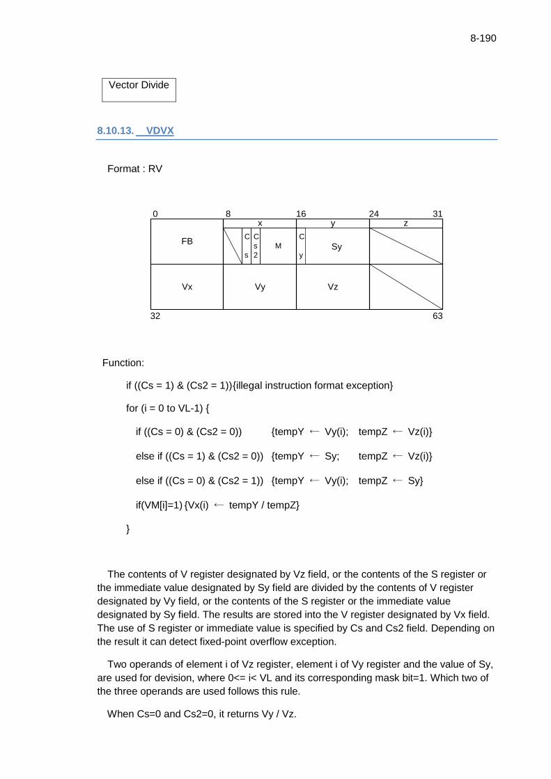
8-190
Vector Divide
8.10.13. VDVX
Format : RV
x
FB Sy
y
C
y
z8 16 24 31
32 63
0
Vx Vy Vz
M
C
s
C
s
2
Function:
if ((Cs = 1) & (Cs2 = 1)) {illegal instruction format exception}
for (i = 0 to VL-1) {
if ((Cs = 0) & (Cs2 = 0)) {tempY ← Vy(i); tempZ ← Vz(i)}
else if ((Cs = 1) & (Cs2 = 0)) {tempY ← Sy; tempZ ← Vz(i)}
else if ((Cs = 0) & (Cs2 = 1)) {tempY ← Vy(i); tempZ ← Sy}
if(VM[i]=1) {Vx(i) ← tempY / tempZ}
}
The contents of V register designated by Vz field, or the contents of the S register or
the immediate value designated by Sy field are divided by the contents of V register
designated by Vy field, or the contents of the S register or the immediate value
designated by Sy field. The results are stored into the V register designated by Vx field.
The use of S register or immediate value is specified by Cs and Cs2 field. Depending on
the result it can detect fixed-point overflow exception.
Two operands of element i of Vz register, element i of Vy register and the value of Sy,
are used for devision, where 0<= i< VL and its corresponding mask bit=1. Which two of
the three operands are used follows this rule.
When Cs=0 and Cs2=0, it returns Vy / Vz.
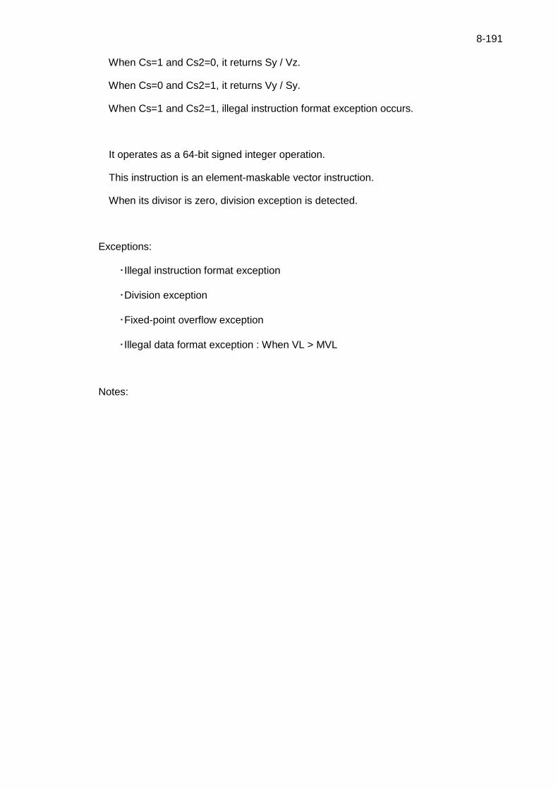
8-191
When Cs=1 and Cs2=0, it returns Sy / Vz.
When Cs=0 and Cs2=1, it returns Vy / Sy.
When Cs=1 and Cs2=1, illegal instruction format exception occurs.
It operates as a 64-bit signed integer operation.
This instruction is an element-maskable vector instruction.
When its divisor is zero, division exception is detected.
Exceptions:
・Illegal instruction format exception
・Division exception
・Fixed-point overflow exception
・Illegal data format exception : When VL > MVL
Notes:
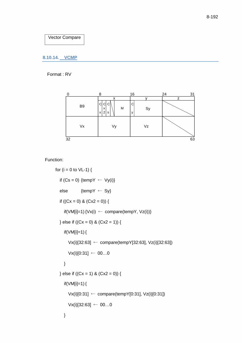
8-192
Vector Compare
8.10.14. VCMP
Format : RV
x
B9 Sy
y
C
y
z8 16 24 31
32 63
0
Vx Vy Vz
M
C
s
C
x
C
x
2
Function:
for (i = 0 to VL-1) {
if (Cs = 0) {tempY ← Vy(i)}
else {tempY ← Sy}
if ((Cx = 0) & (Cx2 = 0)) {
if(VM[i]=1) {Vx(i) ← compare(tempY, Vz(i))}
} else if ((Cx = 0) & (Cx2 = 1)) {
if(VM[i]=1) {
Vx(i)[32:63] ← compare(tempY[32:63], Vz(i)[32:63])
Vx(i)[0:31] ← 00…0
}
} else if ((Cx = 1) & (Cx2 = 0)) {
if(VM[i]=1) {
Vx(i)[0:31] ← compare(tempY[0:31], Vz(i)[0:31])
Vx(i)[32:63] ← 00…0
}
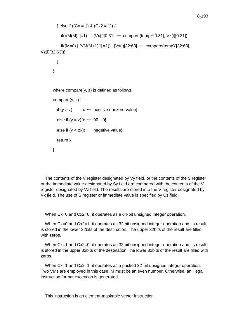
8-193
} else if ((Cx = 1) & (Cx2 = 1)) {
if(VM(M)[i]=1) {Vx(i)[0:31] ← compare(tempY[0:31], Vz(i)[0:31])}
if((M=0) | (VM(M+1)[i] =1)) {Vx(i)[32:63] ← compare(tempY[32:63],
Vz(i)[32:63])}
}
}
where compare(y, z) is defined as follows.
compare(y, z) {
if (y > z) {x ← positive nonzero value}
else if (y = z) {x ← 00…0}
else if (y < z) {x ← negative value}
return x
}
The contents of the V register designated by Vy field, or the contents of the S register
or the immediate value designated by Sy field are compared with the contents of the V
register designated by Vz field. The results are stored into the V register designated by
Vx field. The use of S register or immediate value is specified by Cs field.
When Cx=0 and Cx2=0, it operates as a 64-bit unsigned integer operation.
When Cx=0 and Cx2=1, it operates as 32 bit unsigned integer operation and its result
is stored in the lower 32bits of the destination. The upper 32bits of the result are filled
with zeros.
When Cx=1 and Cx2=0, it operates as 32 bit unsigned integer operation and its result
is stored in the upper 32bits of the destination.The lower 32bits of the result are filled with
zeros.
When Cx=1 and Cx2=1, it operates as a packed 32-bit unsigned integer operation.
Two VMs are employed in this case. M must be an even number. Otherwise, an illegal
instruction format exception is generated.
This instruction is an element-maskable vector instruction.

8-194
Exceptions:
・Illegal instruction format exception
・Illegal data format exception : When VL > MVL
Notes:
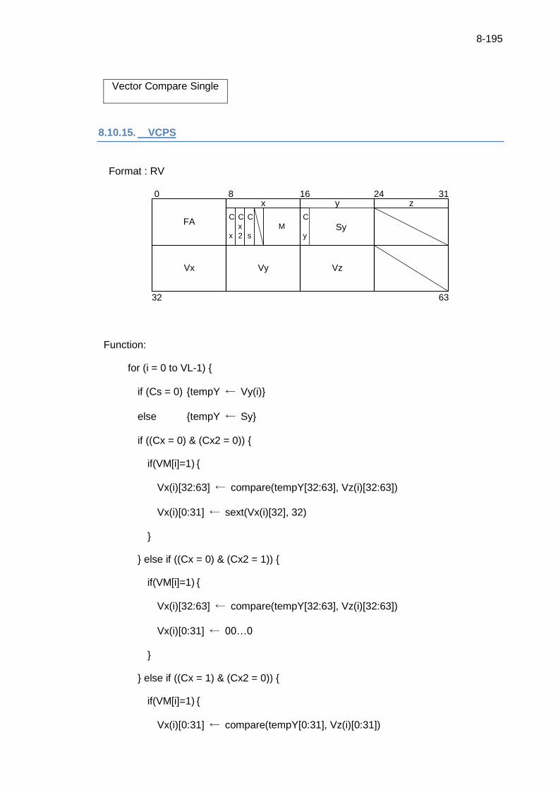
8-195
Vector Compare Single
8.10.15. VCPS
Format : RV
x
FA Sy
y
C
y
z8 16 24 31
32 63
0
Vx Vy Vz
C
x
M
C
s
C
x
2
Function:
for (i = 0 to VL-1) {
if (Cs = 0) {tempY ← Vy(i)}
else {tempY ← Sy}
if ((Cx = 0) & (Cx2 = 0)) {
if(VM[i]=1) {
Vx(i)[32:63] ← compare(tempY[32:63], Vz(i)[32:63])
Vx(i)[0:31] ← sext(Vx(i)[32], 32)
}
} else if ((Cx = 0) & (Cx2 = 1)) {
if(VM[i]=1) {
Vx(i)[32:63] ← compare(tempY[32:63], Vz(i)[32:63])
Vx(i)[0:31] ← 00…0
}
} else if ((Cx = 1) & (Cx2 = 0)) {
if(VM[i]=1) {
Vx(i)[0:31] ← compare(tempY[0:31], Vz(i)[0:31])
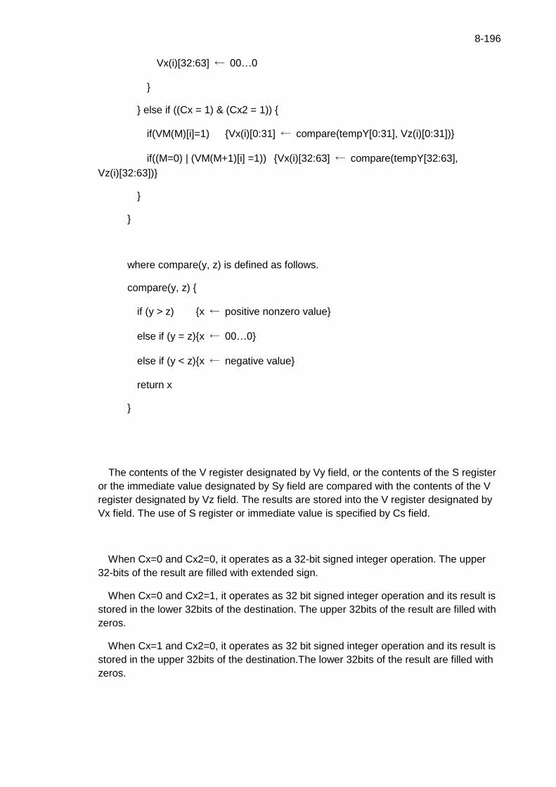
8-196
Vx(i)[32:63] ← 00…0
}
} else if ((Cx = 1) & (Cx2 = 1)) {
if(VM(M)[i]=1) {Vx(i)[0:31] ← compare(tempY[0:31], Vz(i)[0:31])}
if((M=0) | (VM(M+1)[i] =1)) {Vx(i)[32:63] ← compare(tempY[32:63],
Vz(i)[32:63])}
}
}
where compare(y, z) is defined as follows.
compare(y, z) {
if (y > z) {x ← positive nonzero value}
else if (y = z) {x ← 00…0}
else if (y < z) {x ← negative value}
return x
}
The contents of the V register designated by Vy field, or the contents of the S register
or the immediate value designated by Sy field are compared with the contents of the V
register designated by Vz field. The results are stored into the V register designated by
Vx field. The use of S register or immediate value is specified by Cs field.
When Cx=0 and Cx2=0, it operates as a 32-bit signed integer operation. The upper
32-bits of the result are filled with extended sign.
When Cx=0 and Cx2=1, it operates as 32 bit signed integer operation and its result is
stored in the lower 32bits of the destination. The upper 32bits of the result are filled with
zeros.
When Cx=1 and Cx2=0, it operates as 32 bit signed integer operation and its result is
stored in the upper 32bits of the destination.The lower 32bits of the result are filled with
zeros.
8-197
When Cx=1 and Cx2=1, it operates as a packed 32-bit signed integer operation. Two
VMs are employed in this case. M must be an even number. Otherwise, an illegal
instruction format exception is generated.
This instruction is an element-maskable vector instruction.
Exceptions:
・Illegal instruction format exception
・Illegal data format exception : When VL > MVL
Notes:
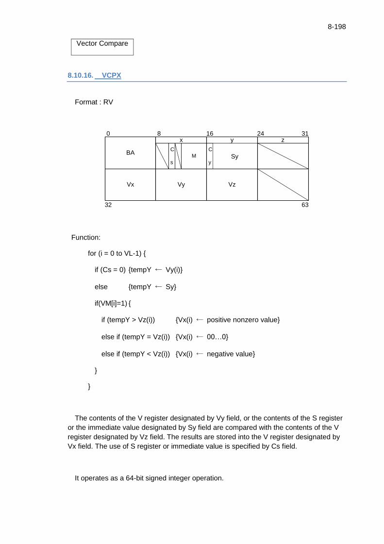
8-198
Vector Compare
8.10.16. VCPX
Format : RV
x
BA Sy
y
C
y
z8 16 24 31
32 63
0
Vx Vy Vz
M
C
s
Function:
for (i = 0 to VL-1) {
if (Cs = 0) {tempY ← Vy(i)}
else {tempY ← Sy}
if(VM[i]=1) {
if (tempY > Vz(i)) {Vx(i) ← positive nonzero value}
else if (tempY = Vz(i)) {Vx(i) ← 00…0}
else if (tempY < Vz(i)) {Vx(i) ← negative value}
}
}
The contents of the V register designated by Vy field, or the contents of the S register
or the immediate value designated by Sy field are compared with the contents of the V
register designated by Vz field. The results are stored into the V register designated by
Vx field. The use of S register or immediate value is specified by Cs field.
It operates as a 64-bit signed integer operation.
8-199
This instruction is an element-maskable vector instruction.
Exceptions:
・Illegal data format exception : When VL > MVL
Notes:
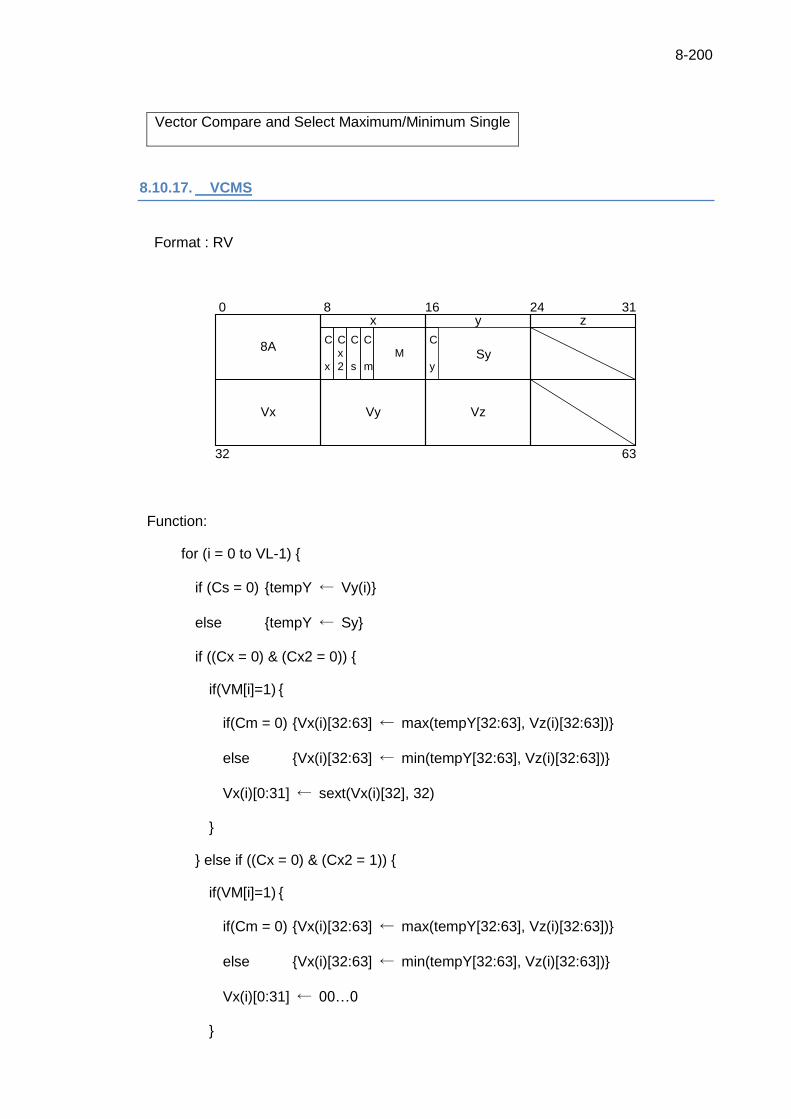
8-200
Vector Compare and Select Maximum/Minimum Single
8.10.17. VCMS
Format : RV
x
8A Sy
y
C
y
z8 16 24 31
32 63
0
Vx Vy Vz
C
x
M
C
s
C
m
C
x
2
Function:
for (i = 0 to VL-1) {
if (Cs = 0) {tempY ← Vy(i)}
else {tempY ← Sy}
if ((Cx = 0) & (Cx2 = 0)) {
if(VM[i]=1) {
if(Cm = 0) {Vx(i)[32:63] ← max(tempY[32:63], Vz(i)[32:63])}
else {Vx(i)[32:63] ← min(tempY[32:63], Vz(i)[32:63])}
Vx(i)[0:31] ← sext(Vx(i)[32], 32)
}
} else if ((Cx = 0) & (Cx2 = 1)) {
if(VM[i]=1) {
if(Cm = 0) {Vx(i)[32:63] ← max(tempY[32:63], Vz(i)[32:63])}
else {Vx(i)[32:63] ← min(tempY[32:63], Vz(i)[32:63])}
Vx(i)[0:31] ← 00…0
}
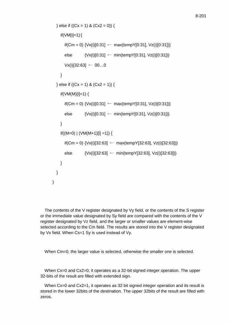
8-201
} else if ((Cx = 1) & (Cx2 = 0)) {
if(VM[i]=1) {
if(Cm = 0) {Vx(i)[0:31] ← max(tempY[0:31], Vz(i)[0:31])}
else {Vx(i)[0:31] ← min(tempY[0:31], Vz(i)[0:31])}
Vx(i)[32:63] ← 00…0
}
} else if ((Cx = 1) & (Cx2 = 1)) {
if(VM(M)[i]=1) {
if(Cm = 0) {Vx(i)[0:31] ← max(tempY[0:31], Vz(i)[0:31])}
else {Vx(i)[0:31] ← min(tempY[0:31], Vz(i)[0:31])}
}
if((M=0) | (VM(M+1)[i] =1)) {
if(Cm = 0) {Vx(i)[32:63] ← max(tempY[32:63], Vz(i)[32:63])}
else {Vx(i)[32:63] ← min(tempY[32:63], Vz(i)[32:63])}
}
}
}
The contents of the V register designated by Vy field, or the contents of the S register
or the immediate value designated by Sy field are compared with the contents of the V
register designated by Vz field, and the larger or smaller values are element-wise
selected according to the Cm field. The results are stored into the V register designated
by Vx field. When Cs=1 Sy is used instead of Vy.
When Cm=0, the larger value is selected, otherwise the smaller one is selected.
When Cx=0 and Cx2=0, it operates as a 32-bit signed integer operation. The upper
32-bits of the result are filled with extended sign.
When Cx=0 and Cx2=1, it operates as 32 bit signed integer operation and its result is
stored in the lower 32bits of the destination. The upper 32bits of the result are filled with
zeros.
8-202
When Cx=1 and Cx2=0, it operates as 32 bit signed integer operation and its result is
stored in the upper 32bits of the destination.The lower 32bits of the result are filled with
zeros.
When Cx=1 and Cx2=1, it operates as a packed 32-bit signed integer operation. Two
VMs are employed in this case. M must be an even number. Otherwise, an illegal
instruction format exception occurs.
This instruction is an element-maskable vector instruction.
Exceptions:
・Illegal instruction format exception
・Illegal data format exception : When VL > MVL
Notes:
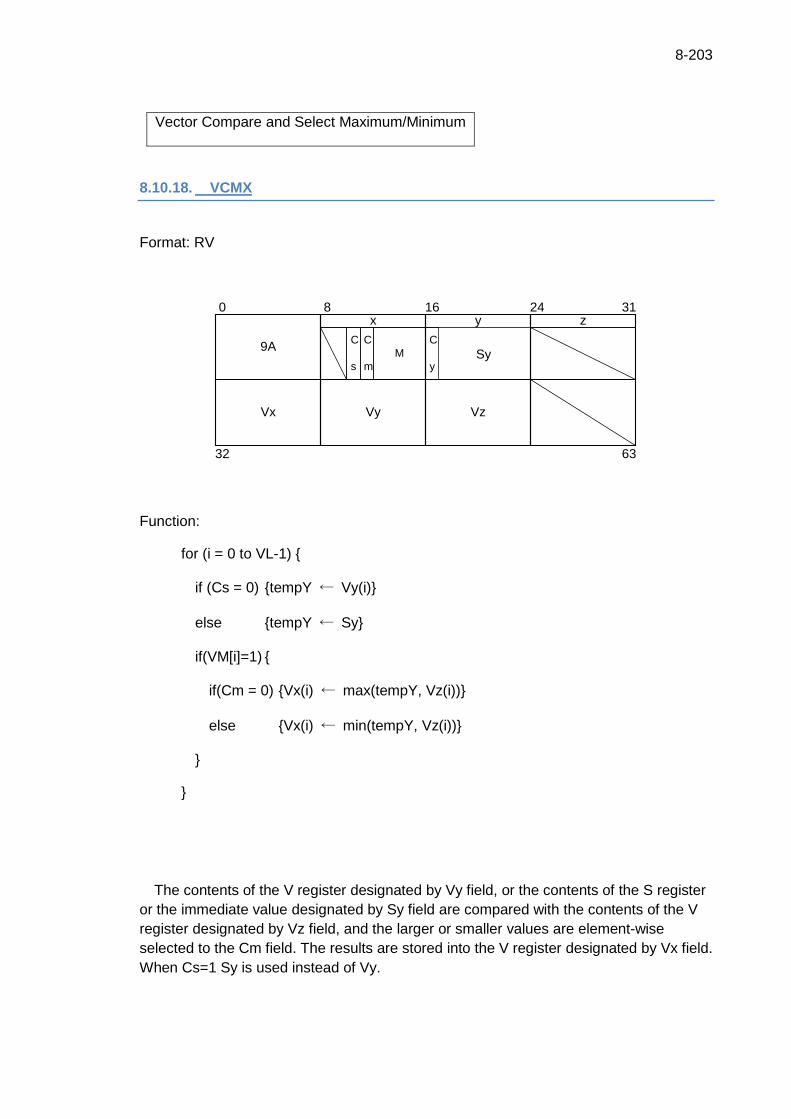
8-203
Vector Compare and Select Maximum/Minimum
8.10.18. VCMX
Format: RV
x
9A Sy
y
C
y
z8 16 24 31
32 63
0
Vx Vy Vz
M
C
s
C
m
Function:
for (i = 0 to VL-1) {
if (Cs = 0) {tempY ← Vy(i)}
else {tempY ← Sy}
if(VM[i]=1) {
if(Cm = 0) {Vx(i) ← max(tempY, Vz(i))}
else {Vx(i) ← min(tempY, Vz(i))}
}
}
The contents of the V register designated by Vy field, or the contents of the S register
or the immediate value designated by Sy field are compared with the contents of the V
register designated by Vz field, and the larger or smaller values are element-wise
selected to the Cm field. The results are stored into the V register designated by Vx field.
When Cs=1 Sy is used instead of Vy.
8-204
When Cm=0, the larger value is selected as the result, otherwise the smaller value is
selected.
It operates as a 64-bit signed integer operation.
This instruction is an element-maskable vector instruction.
Exceptions:
・Illegal data format exception : When VL > MVL
Notes:
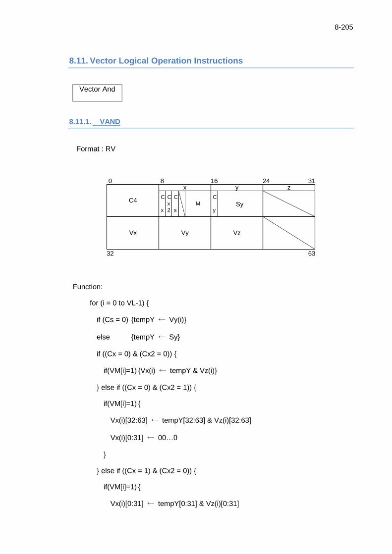
8-205
8.11. Vector Logical Operation Instructions
Vector And
8.11.1. VAND
Format : RV
x
C4 Sy
y
C
y
z8 16 24 31
32 63
0
Vx Vy Vz
M
C
s
C
x
C
x
2
Function:
for (i = 0 to VL-1) {
if (Cs = 0) {tempY ← Vy(i)}
else {tempY ← Sy}
if ((Cx = 0) & (Cx2 = 0)) {
if(VM[i]=1) {Vx(i) ← tempY & Vz(i)}
} else if ((Cx = 0) & (Cx2 = 1)) {
if(VM[i]=1) {
Vx(i)[32:63] ← tempY[32:63] & Vz(i)[32:63]
Vx(i)[0:31] ← 00…0
}
} else if ((Cx = 1) & (Cx2 = 0)) {
if(VM[i]=1) {
Vx(i)[0:31] ← tempY[0:31] & Vz(i)[0:31]
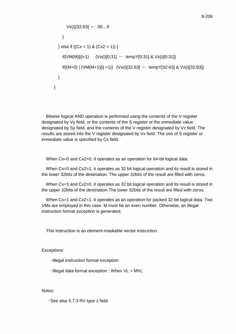
8-206
Vx(i)[32:63] ← 00…0
}
} else if ((Cx = 1) & (Cx2 = 1)) {
if(VM(M)[i]=1) {Vx(i)[0:31] ← tempY[0:31] & Vz(i)[0:31]}
if((M=0) | (VM(M+1)[i] =1)) {Vx(i)[32:63] ← tempY[32:63] & Vz(i)[32:63]}
}
}
Bitwise logical AND operation is performed using the contents of the V register
designated by Vy field, or the contents of the S register or the immediate value
designated by Sy field, and the contents of the V register designated by Vz field. The
results are stored into the V register designated by Vx field. The use of S register or
immediate value is specified by Cs field.
When Cx=0 and Cx2=0, it operates as an operation for 64-bit logical data.
When Cx=0 and Cx2=1, it operates as 32 bit logical operation and its result is stored in
the lower 32bits of the destination. The upper 32bits of the result are filled with zeros.
When Cx=1 and Cx2=0, it operates as 32 bit logical operation and its result is stored in
the upper 32bits of the destination.The lower 32bits of the result are filled with zeros.
When Cx=1 and Cx2=1, it operates as an operation for packed 32-bit logical data. Two
VMs are employed in this case. M must be an even number. Otherwise, an illegal
instruction format exception is generated.
This instruction is an element-maskable vector instruction.
Exceptions:
・Illegal instruction format exception
・Illegal data format exception : When VL > MVL
Notes:
・See also 5.7.3 RV type z field.
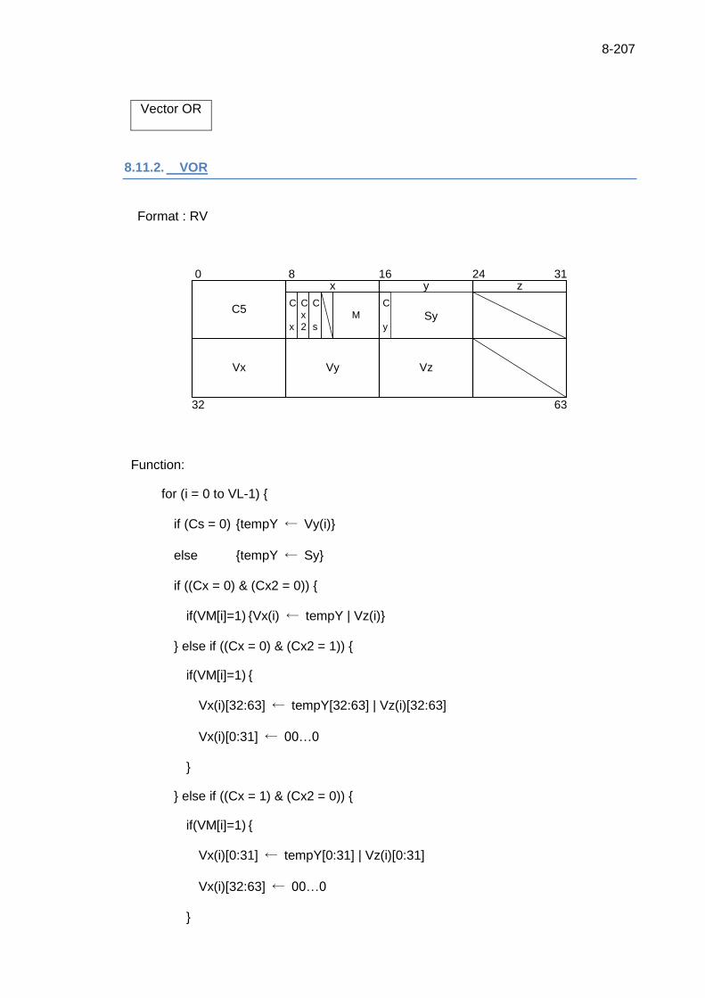
8-207
Vector OR
8.11.2. VOR
Format : RV
x
C5 Sy
y
C
y
z8 16 24 31
32 63
0
Vx Vy Vz
M
C
s
C
x
C
x
2
Function:
for (i = 0 to VL-1) {
if (Cs = 0) {tempY ← Vy(i)}
else {tempY ← Sy}
if ((Cx = 0) & (Cx2 = 0)) {
if(VM[i]=1) {Vx(i) ← tempY | Vz(i)}
} else if ((Cx = 0) & (Cx2 = 1)) {
if(VM[i]=1) {
Vx(i)[32:63] ← tempY[32:63] | Vz(i)[32:63]
Vx(i)[0:31] ← 00…0
}
} else if ((Cx = 1) & (Cx2 = 0)) {
if(VM[i]=1) {
Vx(i)[0:31] ← tempY[0:31] | Vz(i)[0:31]
Vx(i)[32:63] ← 00…0
}
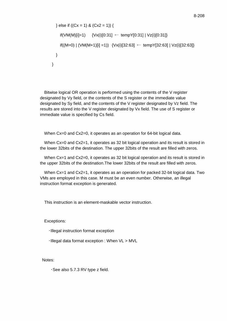
8-208
} else if ((Cx = 1) & (Cx2 = 1)) {
if(VM(M)[i]=1) {Vx(i)[0:31] ← tempY[0:31] | Vz(i)[0:31]}
if((M=0) | (VM(M+1)[i] =1)) {Vx(i)[32:63] ← tempY[32:63] | Vz(i)[32:63]}
}
}
Bitwise logical OR operation is performed using the contents of the V register
designated by Vy field, or the contents of the S register or the immediate value
designated by Sy field, and the contents of the V register designated by Vz field. The
results are stored into the V register designated by Vx field. The use of S register or
immediate value is specified by Cs field.
When Cx=0 and Cx2=0, it operates as an operation for 64-bit logical data.
When Cx=0 and Cx2=1, it operates as 32 bit logical operation and its result is stored in
the lower 32bits of the destination. The upper 32bits of the result are filled with zeros.
When Cx=1 and Cx2=0, it operates as 32 bit logical operation and its result is stored in
the upper 32bits of the destination.The lower 32bits of the result are filled with zeros.
When Cx=1 and Cx2=1, it operates as an operation for packed 32-bit logical data. Two
VMs are employed in this case. M must be an even number. Otherwise, an illegal
instruction format exception is generated.
This instruction is an element-maskable vector instruction.
Exceptions:
・Illegal instruction format exception
・Illegal data format exception : When VL > MVL
Notes:
・See also 5.7.3 RV type z field.
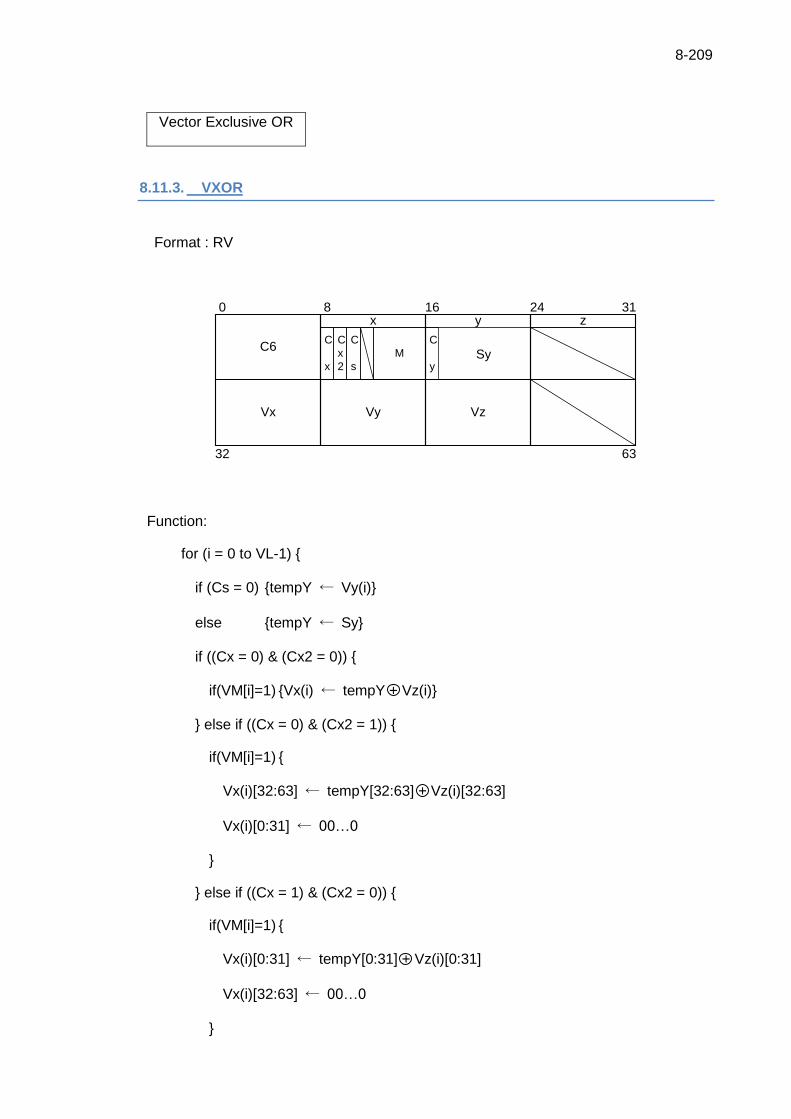
8-209
Vector Exclusive OR
8.11.3. VXOR
Format : RV
x
C6 Sy
y
C
y
z8 16 24 31
32 63
0
Vx Vy Vz
M
C
s
C
x
C
x
2
Function:
for (i = 0 to VL-1) {
if (Cs = 0) {tempY ← Vy(i)}
else {tempY ← Sy}
if ((Cx = 0) & (Cx2 = 0)) {
if(VM[i]=1) {Vx(i) ← tempY + Vz(i)}
} else if ((Cx = 0) & (Cx2 = 1)) {
if(VM[i]=1) {
Vx(i)[32:63] ← tempY[32:63] + Vz(i)[32:63]
Vx(i)[0:31] ← 00…0
}
} else if ((Cx = 1) & (Cx2 = 0)) {
if(VM[i]=1) {
Vx(i)[0:31] ← tempY[0:31] + Vz(i)[0:31]
Vx(i)[32:63] ← 00…0
}
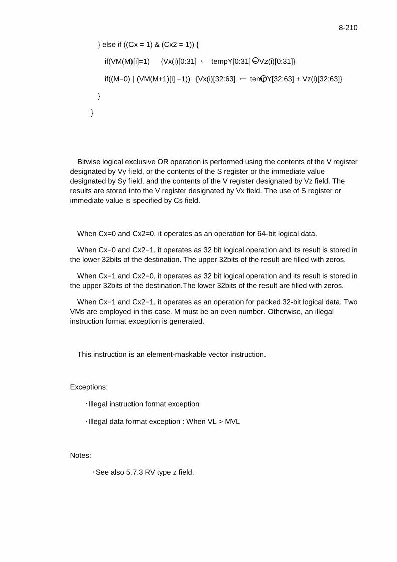
8-210
} else if ((Cx = 1) & (Cx2 = 1)) {
if(VM(M)[i]=1) {Vx(i)[0:31] ← tempY[0:31] + Vz(i)[0:31]}
if((M=0) | (VM(M+1)[i] =1)) {Vx(i)[32:63] ← tempY[32:63] + Vz(i)[32:63]}
}
}
Bitwise logical exclusive OR operation is performed using the contents of the V register
designated by Vy field, or the contents of the S register or the immediate value
designated by Sy field, and the contents of the V register designated by Vz field. The
results are stored into the V register designated by Vx field. The use of S register or
immediate value is specified by Cs field.
When Cx=0 and Cx2=0, it operates as an operation for 64-bit logical data.
When Cx=0 and Cx2=1, it operates as 32 bit logical operation and its result is stored in
the lower 32bits of the destination. The upper 32bits of the result are filled with zeros.
When Cx=1 and Cx2=0, it operates as 32 bit logical operation and its result is stored in
the upper 32bits of the destination.The lower 32bits of the result are filled with zeros.
When Cx=1 and Cx2=1, it operates as an operation for packed 32-bit logical data. Two
VMs are employed in this case. M must be an even number. Otherwise, an illegal
instruction format exception is generated.
This instruction is an element-maskable vector instruction.
Exceptions:
・Illegal instruction format exception
・Illegal data format exception : When VL > MVL
Notes:
・See also 5.7.3 RV type z field.
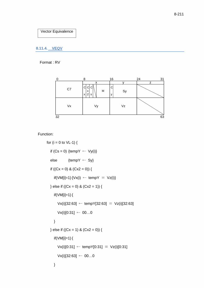
8-211
Vector Equivalence
8.11.4. VEQV
Format : RV
x
C7 Sy
y
C
y
z8 16 24 31
32 63
0
Vx Vy Vz
M
C
s
C
x
C
x
2
Function:
for (i = 0 to VL-1) {
if (Cs = 0) {tempY ← Vy(i)}
else {tempY ← Sy}
if ((Cx = 0) & (Cx2 = 0)) {
if(VM[i]=1) {Vx(i) ← tempY ≡ Vz(i)}
} else if ((Cx = 0) & (Cx2 = 1)) {
if(VM[i]=1) {
Vx(i)[32:63] ← tempY[32:63] ≡ Vz(i)[32:63]
Vx(i)[0:31] ← 00…0
}
} else if ((Cx = 1) & (Cx2 = 0)) {
if(VM[i]=1) {
Vx(i)[0:31] ← tempY[0:31] ≡ Vz(i)[0:31]
Vx(i)[32:63] ← 00…0
}
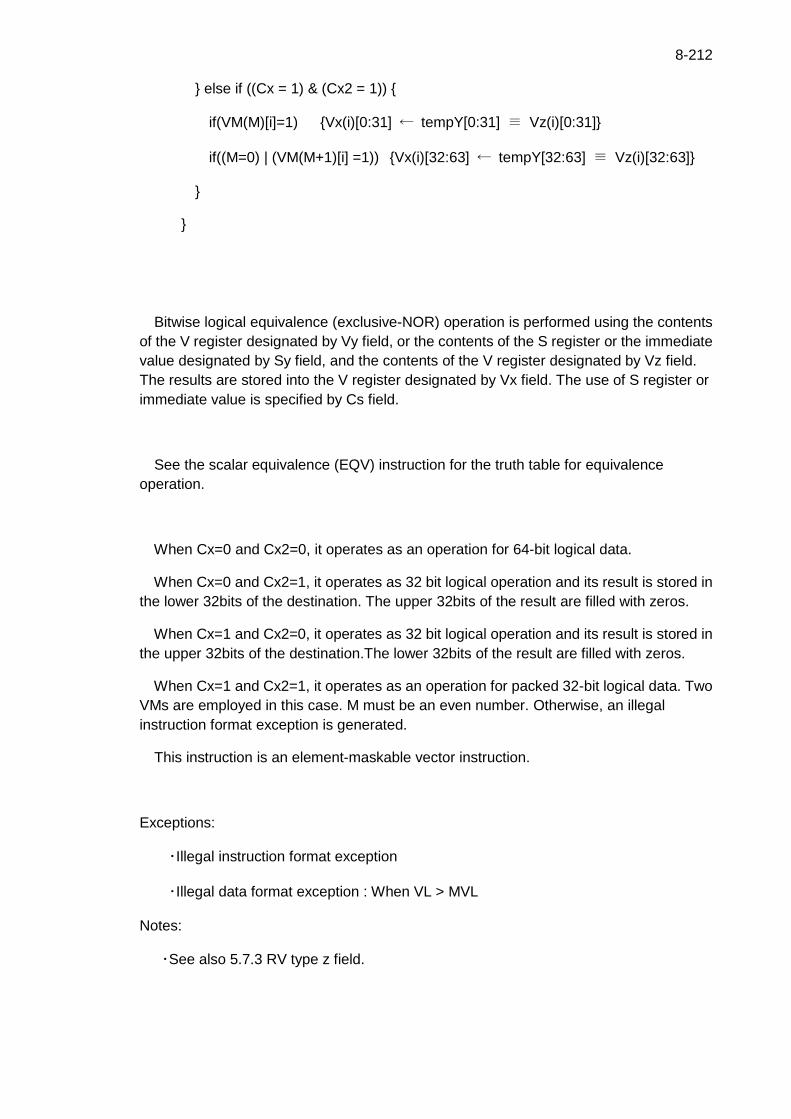
8-212
} else if ((Cx = 1) & (Cx2 = 1)) {
if(VM(M)[i]=1) {Vx(i)[0:31] ← tempY[0:31] ≡ Vz(i)[0:31]}
if((M=0) | (VM(M+1)[i] =1)) {Vx(i)[32:63] ← tempY[32:63] ≡ Vz(i)[32:63]}
}
}
Bitwise logical equivalence (exclusive-NOR) operation is performed using the contents
of the V register designated by Vy field, or the contents of the S register or the immediate
value designated by Sy field, and the contents of the V register designated by Vz field.
The results are stored into the V register designated by Vx field. The use of S register or
immediate value is specified by Cs field.
See the scalar equivalence (EQV) instruction for the truth table for equivalence
operation.
When Cx=0 and Cx2=0, it operates as an operation for 64-bit logical data.
When Cx=0 and Cx2=1, it operates as 32 bit logical operation and its result is stored in
the lower 32bits of the destination. The upper 32bits of the result are filled with zeros.
When Cx=1 and Cx2=0, it operates as 32 bit logical operation and its result is stored in
the upper 32bits of the destination.The lower 32bits of the result are filled with zeros.
When Cx=1 and Cx2=1, it operates as an operation for packed 32-bit logical data. Two
VMs are employed in this case. M must be an even number. Otherwise, an illegal
instruction format exception is generated.
This instruction is an element-maskable vector instruction.
Exceptions:
・Illegal instruction format exception
・Illegal data format exception : When VL > MVL
Notes:
・See also 5.7.3 RV type z field.
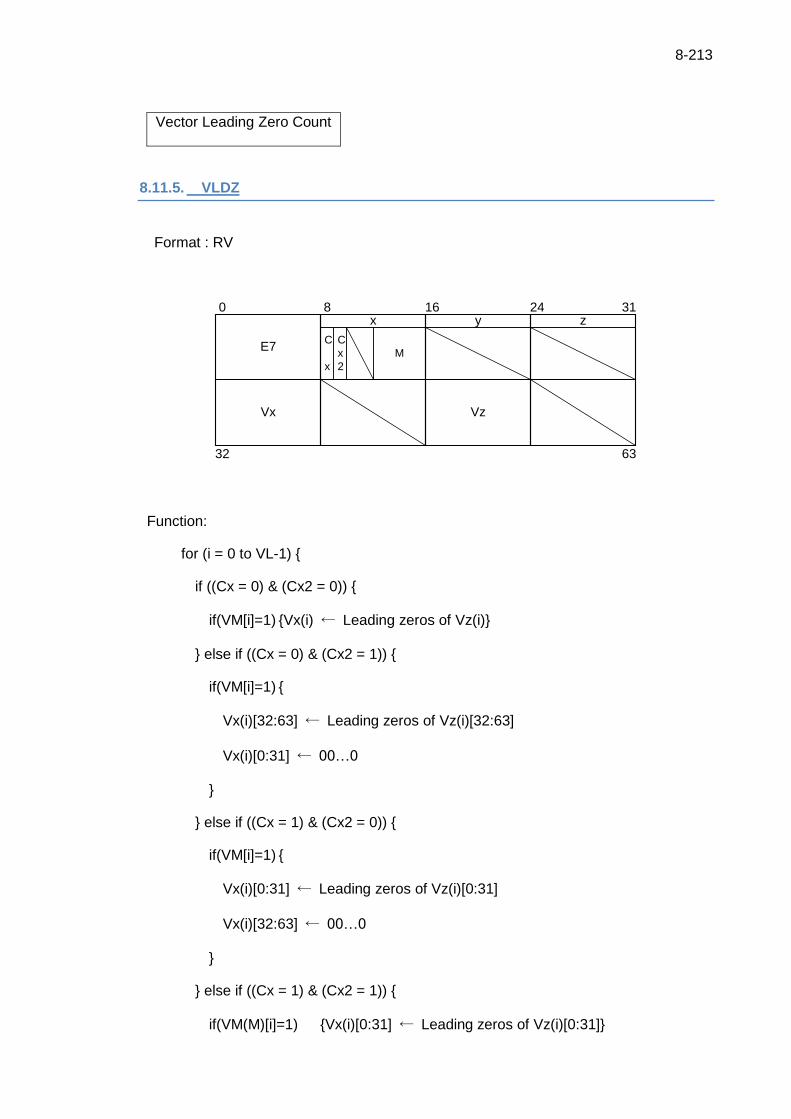
8-213
Vector Leading Zero Count
8.11.5. VLDZ
Format : RV
x
E7
y z8 16 24 31
32 63
0
Vx Vz
M
C
x
C
x
2
Function:
for (i = 0 to VL-1) {
if ((Cx = 0) & (Cx2 = 0)) {
if(VM[i]=1) {Vx(i) ← Leading zeros of Vz(i)}
} else if ((Cx = 0) & (Cx2 = 1)) {
if(VM[i]=1) {
Vx(i)[32:63] ← Leading zeros of Vz(i)[32:63]
Vx(i)[0:31] ← 00…0
}
} else if ((Cx = 1) & (Cx2 = 0)) {
if(VM[i]=1) {
Vx(i)[0:31] ← Leading zeros of Vz(i)[0:31]
Vx(i)[32:63] ← 00…0
}
} else if ((Cx = 1) & (Cx2 = 1)) {
if(VM(M)[i]=1) {Vx(i)[0:31] ← Leading zeros of Vz(i)[0:31]}
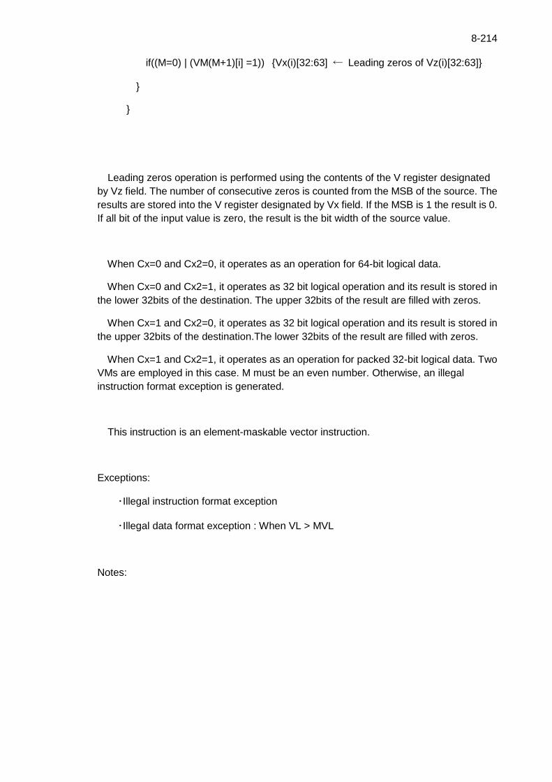
8-214
if((M=0) | (VM(M+1)[i] =1)) {Vx(i)[32:63] ← Leading zeros of Vz(i)[32:63]}
}
}
Leading zeros operation is performed using the contents of the V register designated
by Vz field. The number of consecutive zeros is counted from the MSB of the source. The
results are stored into the V register designated by Vx field. If the MSB is 1 the result is 0.
If all bit of the input value is zero, the result is the bit width of the source value.
When Cx=0 and Cx2=0, it operates as an operation for 64-bit logical data.
When Cx=0 and Cx2=1, it operates as 32 bit logical operation and its result is stored in
the lower 32bits of the destination. The upper 32bits of the result are filled with zeros.
When Cx=1 and Cx2=0, it operates as 32 bit logical operation and its result is stored in
the upper 32bits of the destination.The lower 32bits of the result are filled with zeros.
When Cx=1 and Cx2=1, it operates as an operation for packed 32-bit logical data. Two
VMs are employed in this case. M must be an even number. Otherwise, an illegal
instruction format exception is generated.
This instruction is an element-maskable vector instruction.
Exceptions:
・Illegal instruction format exception
・Illegal data format exception : When VL > MVL
Notes:
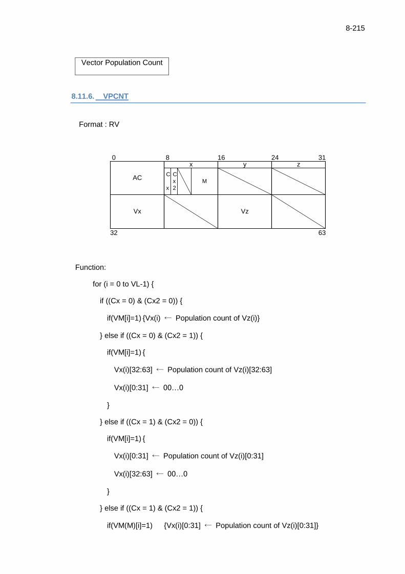
8-215
Vector Population Count
8.11.6. VPCNT
Format : RV
x
AC
y z8 16 24 31
32 63
0
Vx Vz
M
C
x
C
x
2
Function:
for (i = 0 to VL-1) {
if ((Cx = 0) & (Cx2 = 0)) {
if(VM[i]=1) {Vx(i) ← Population count of Vz(i)}
} else if ((Cx = 0) & (Cx2 = 1)) {
if(VM[i]=1) {
Vx(i)[32:63] ← Population count of Vz(i)[32:63]
Vx(i)[0:31] ← 00…0
}
} else if ((Cx = 1) & (Cx2 = 0)) {
if(VM[i]=1) {
Vx(i)[0:31] ← Population count of Vz(i)[0:31]
Vx(i)[32:63] ← 00…0
}
} else if ((Cx = 1) & (Cx2 = 1)) {
if(VM(M)[i]=1) {Vx(i)[0:31] ← Population count of Vz(i)[0:31]}
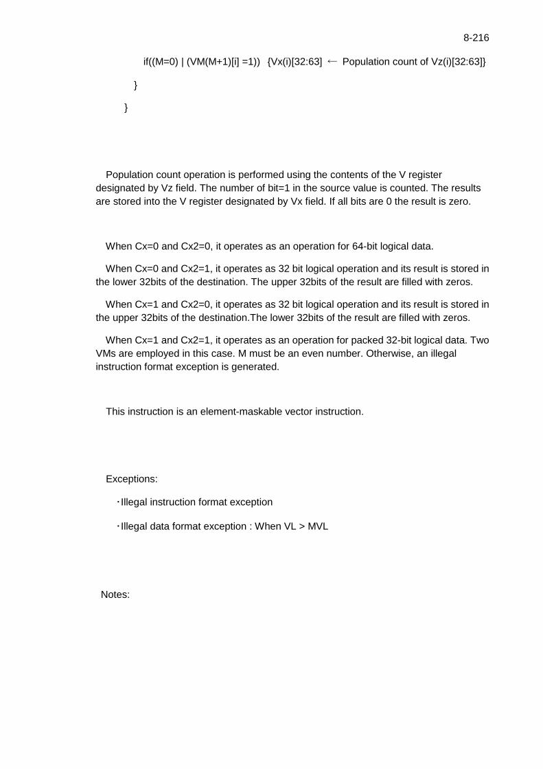
8-216
if((M=0) | (VM(M+1)[i] =1)) {Vx(i)[32:63] ← Population count of Vz(i)[32:63]}
}
}
Population count operation is performed using the contents of the V register
designated by Vz field. The number of bit=1 in the source value is counted. The results
are stored into the V register designated by Vx field. If all bits are 0 the result is zero.
When Cx=0 and Cx2=0, it operates as an operation for 64-bit logical data.
When Cx=0 and Cx2=1, it operates as 32 bit logical operation and its result is stored in
the lower 32bits of the destination. The upper 32bits of the result are filled with zeros.
When Cx=1 and Cx2=0, it operates as 32 bit logical operation and its result is stored in
the upper 32bits of the destination.The lower 32bits of the result are filled with zeros.
When Cx=1 and Cx2=1, it operates as an operation for packed 32-bit logical data. Two
VMs are employed in this case. M must be an even number. Otherwise, an illegal
instruction format exception is generated.
This instruction is an element-maskable vector instruction.
Exceptions:
・Illegal instruction format exception
・Illegal data format exception : When VL > MVL
Notes:
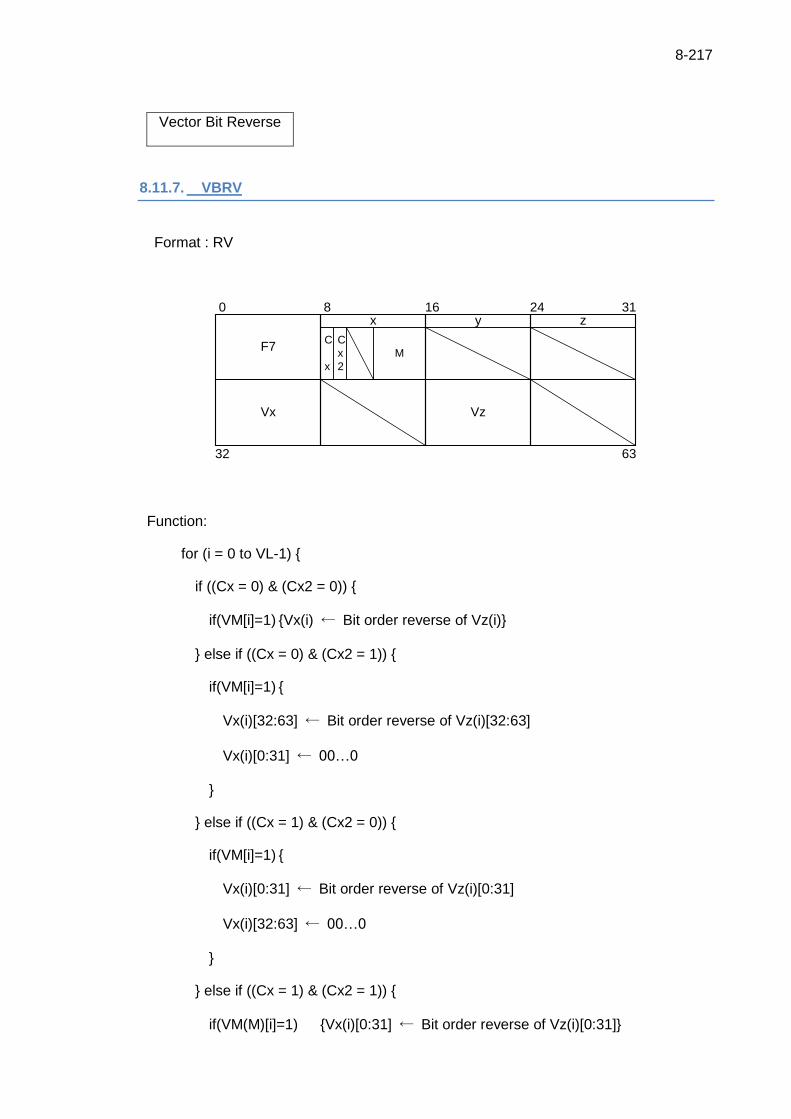
8-217
Vector Bit Reverse
8.11.7. VBRV
Format : RV
x
F7
y z8 16 24 31
32 63
0
Vx Vz
M
C
x
C
x
2
Function:
for (i = 0 to VL-1) {
if ((Cx = 0) & (Cx2 = 0)) {
if(VM[i]=1) {Vx(i) ← Bit order reverse of Vz(i)}
} else if ((Cx = 0) & (Cx2 = 1)) {
if(VM[i]=1) {
Vx(i)[32:63] ← Bit order reverse of Vz(i)[32:63]
Vx(i)[0:31] ← 00…0
}
} else if ((Cx = 1) & (Cx2 = 0)) {
if(VM[i]=1) {
Vx(i)[0:31] ← Bit order reverse of Vz(i)[0:31]
Vx(i)[32:63] ← 00…0
}
} else if ((Cx = 1) & (Cx2 = 1)) {
if(VM(M)[i]=1) {Vx(i)[0:31] ← Bit order reverse of Vz(i)[0:31]}
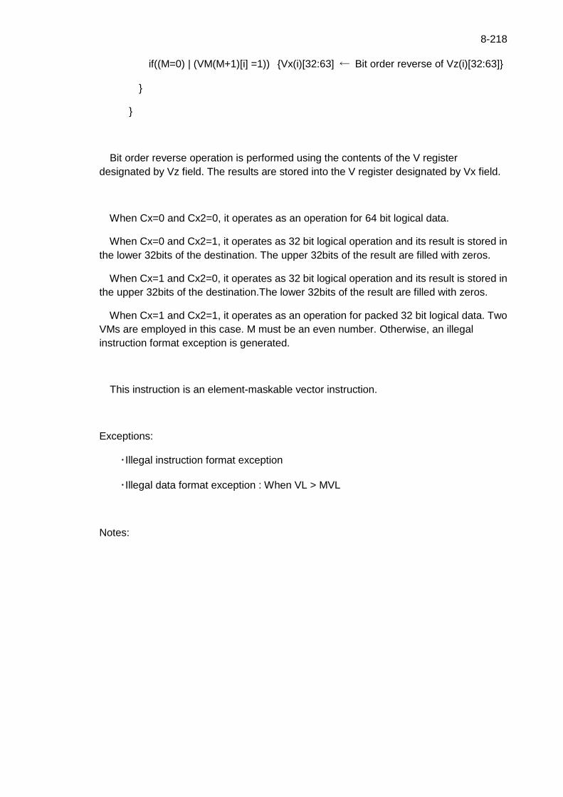
8-218
if((M=0) | (VM(M+1)[i] =1)) {Vx(i)[32:63] ← Bit order reverse of Vz(i)[32:63]}
}
}
Bit order reverse operation is performed using the contents of the V register
designated by Vz field. The results are stored into the V register designated by Vx field.
When Cx=0 and Cx2=0, it operates as an operation for 64 bit logical data.
When Cx=0 and Cx2=1, it operates as 32 bit logical operation and its result is stored in
the lower 32bits of the destination. The upper 32bits of the result are filled with zeros.
When Cx=1 and Cx2=0, it operates as 32 bit logical operation and its result is stored in
the upper 32bits of the destination.The lower 32bits of the result are filled with zeros.
When Cx=1 and Cx2=1, it operates as an operation for packed 32 bit logical data. Two
VMs are employed in this case. M must be an even number. Otherwise, an illegal
instruction format exception is generated.
This instruction is an element-maskable vector instruction.
Exceptions:
・Illegal instruction format exception
・Illegal data format exception : When VL > MVL
Notes:
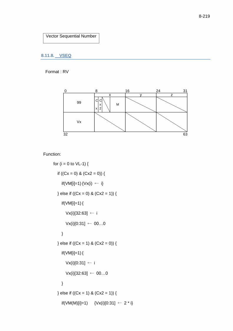
8-219
Vector Sequential Number
8.11.8. VSEQ
Format : RV
x
99
y z8 16 24 31
32 63
0
Vx
M
C
x
C
x
2
Function:
for (i = 0 to VL-1) {
if ((Cx = 0) & (Cx2 = 0)) {
if(VM[i]=1) {Vx(i) ← i}
} else if ((Cx = 0) & (Cx2 = 1)) {
if(VM[i]=1) {
Vx(i)[32:63] ← i
Vx(i)[0:31] ← 00…0
}
} else if ((Cx = 1) & (Cx2 = 0)) {
if(VM[i]=1) {
Vx(i)[0:31] ← i
Vx(i)[32:63] ← 00…0
}
} else if ((Cx = 1) & (Cx2 = 1)) {
if(VM(M)[i]=1) {Vx(i)[0:31] ← 2 * i}
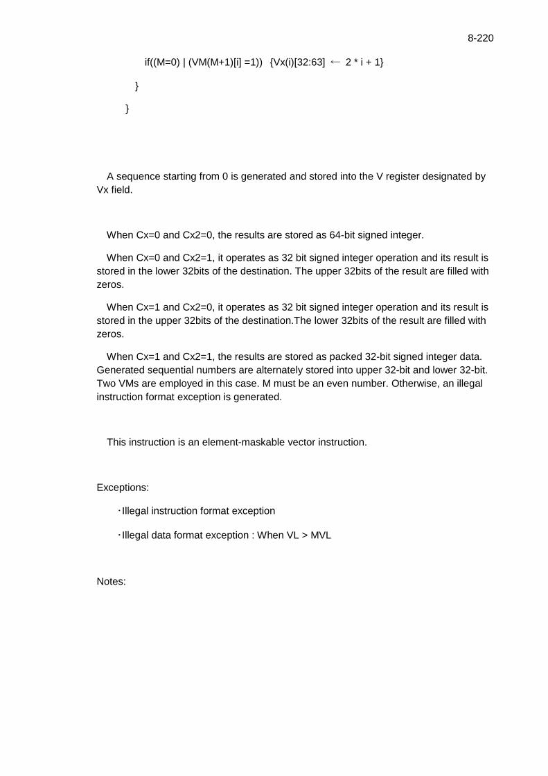
8-220
if((M=0) | (VM(M+1)[i] =1)) {Vx(i)[32:63] ← 2 * i + 1}
}
}
A sequence starting from 0 is generated and stored into the V register designated by
Vx field.
When Cx=0 and Cx2=0, the results are stored as 64-bit signed integer.
When Cx=0 and Cx2=1, it operates as 32 bit signed integer operation and its result is
stored in the lower 32bits of the destination. The upper 32bits of the result are filled with
zeros.
When Cx=1 and Cx2=0, it operates as 32 bit signed integer operation and its result is
stored in the upper 32bits of the destination.The lower 32bits of the result are filled with
zeros.
When Cx=1 and Cx2=1, the results are stored as packed 32-bit signed integer data.
Generated sequential numbers are alternately stored into upper 32-bit and lower 32-bit.
Two VMs are employed in this case. M must be an even number. Otherwise, an illegal
instruction format exception is generated.
This instruction is an element-maskable vector instruction.
Exceptions:
・Illegal instruction format exception
・Illegal data format exception : When VL > MVL
Notes:
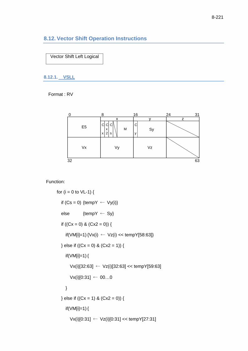
8-221
8.12. Vector Shift Operation Instructions
Vector Shift Left Logical
8.12.1. VSLL
Format : RV
x
E5 Sy
y
C
y
z8 16 24 31
32 63
0
Vx Vy Vz
M
C
s
C
x
C
x
2
Function:
for (i = 0 to VL-1) {
if (Cs = 0) {tempY ← Vy(i)}
else {tempY ← Sy}
if ((Cx = 0) & (Cx2 = 0)) {
if(VM[i]=1) {Vx(i) ← Vz(i) << tempY[58:63]}
} else if ((Cx = 0) & (Cx2 = 1)) {
if(VM[i]=1) {
Vx(i)[32:63] ← Vz(i)[32:63] << tempY[59:63]
Vx(i)[0:31] ← 00…0
}
} else if ((Cx = 1) & (Cx2 = 0)) {
if(VM[i]=1) {
Vx(i)[0:31] ← Vz(i)[0:31] << tempY[27:31]
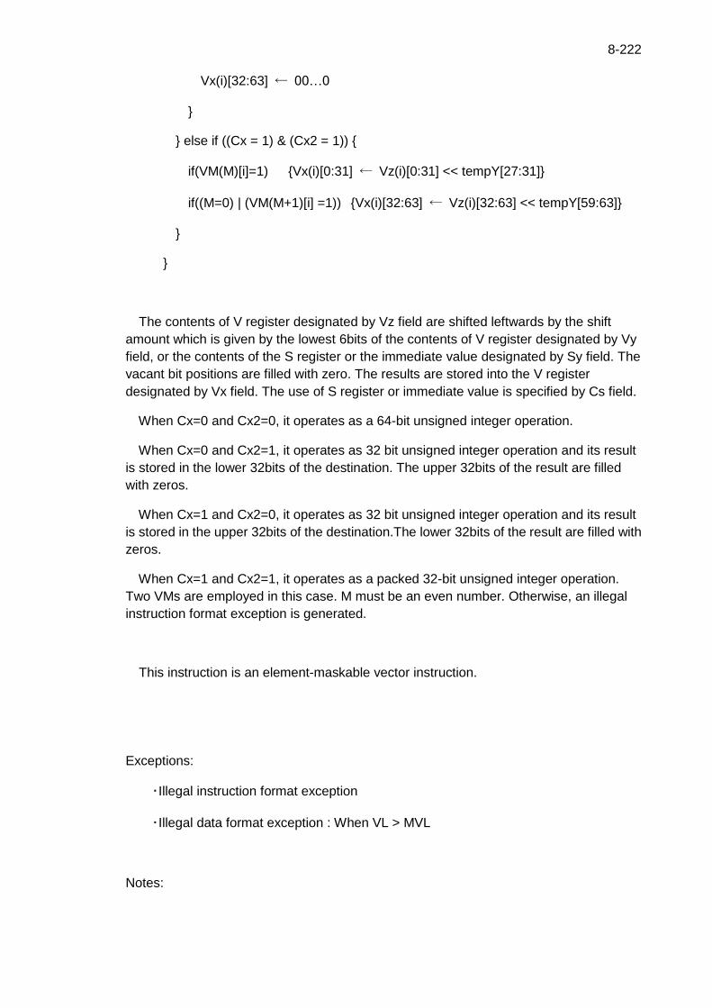
8-222
Vx(i)[32:63] ← 00…0
}
} else if ((Cx = 1) & (Cx2 = 1)) {
if(VM(M)[i]=1) {Vx(i)[0:31] ← Vz(i)[0:31] << tempY[27:31]}
if((M=0) | (VM(M+1)[i] =1)) {Vx(i)[32:63] ← Vz(i)[32:63] << tempY[59:63]}
}
}
The contents of V register designated by Vz field are shifted leftwards by the shift
amount which is given by the lowest 6bits of the contents of V register designated by Vy
field, or the contents of the S register or the immediate value designated by Sy field. The
vacant bit positions are filled with zero. The results are stored into the V register
designated by Vx field. The use of S register or immediate value is specified by Cs field.
When Cx=0 and Cx2=0, it operates as a 64-bit unsigned integer operation.
When Cx=0 and Cx2=1, it operates as 32 bit unsigned integer operation and its result
is stored in the lower 32bits of the destination. The upper 32bits of the result are filled
with zeros.
When Cx=1 and Cx2=0, it operates as 32 bit unsigned integer operation and its result
is stored in the upper 32bits of the destination.The lower 32bits of the result are filled with
zeros.
When Cx=1 and Cx2=1, it operates as a packed 32-bit unsigned integer operation.
Two VMs are employed in this case. M must be an even number. Otherwise, an illegal
instruction format exception is generated.
This instruction is an element-maskable vector instruction.
Exceptions:
・Illegal instruction format exception
・Illegal data format exception : When VL > MVL
Notes:
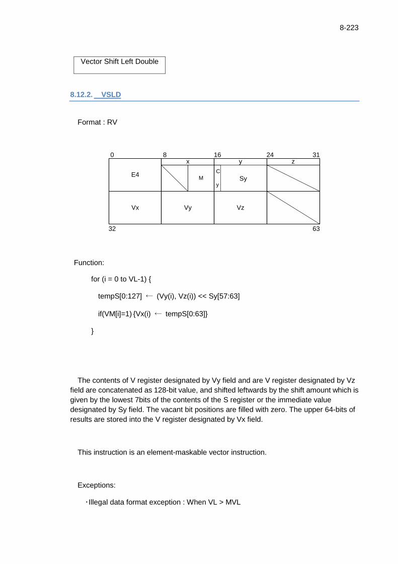
8-223
Vector Shift Left Double
8.12.2. VSLD
Format : RV
x
E4 Sy
y
C
y
z8 16 24 31
32 63
0
Vx Vy Vz
M
Function:
for (i = 0 to VL-1) {
tempS[0:127] ← (Vy(i), Vz(i)) << Sy[57:63]
if(VM[i]=1) {Vx(i) ← tempS[0:63]}
}
The contents of V register designated by Vy field and are V register designated by Vz
field are concatenated as 128-bit value, and shifted leftwards by the shift amount which is
given by the lowest 7bits of the contents of the S register or the immediate value
designated by Sy field. The vacant bit positions are filled with zero. The upper 64-bits of
results are stored into the V register designated by Vx field.
This instruction is an element-maskable vector instruction.
Exceptions:
・Illegal data format exception : When VL > MVL
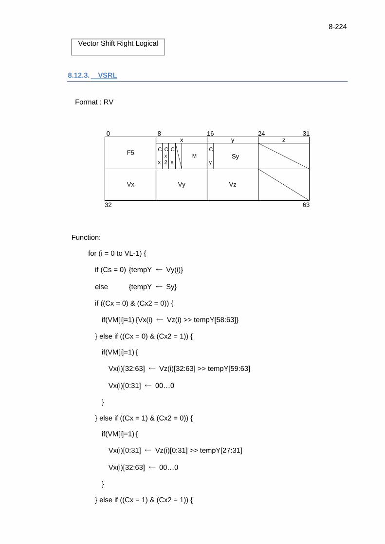
8-224
Vector Shift Right Logical
8.12.3. VSRL
Format : RV
x
F5 Sy
y
C
y
z8 16 24 31
32 63
0
Vx Vy Vz
M
C
s
C
x
C
x
2
Function:
for (i = 0 to VL-1) {
if (Cs = 0) {tempY ← Vy(i)}
else {tempY ← Sy}
if ((Cx = 0) & (Cx2 = 0)) {
if(VM[i]=1) {Vx(i) ← Vz(i) >> tempY[58:63]}
} else if ((Cx = 0) & (Cx2 = 1)) {
if(VM[i]=1) {
Vx(i)[32:63] ← Vz(i)[32:63] >> tempY[59:63]
Vx(i)[0:31] ← 00…0
}
} else if ((Cx = 1) & (Cx2 = 0)) {
if(VM[i]=1) {
Vx(i)[0:31] ← Vz(i)[0:31] >> tempY[27:31]
Vx(i)[32:63] ← 00…0
}
} else if ((Cx = 1) & (Cx2 = 1)) {
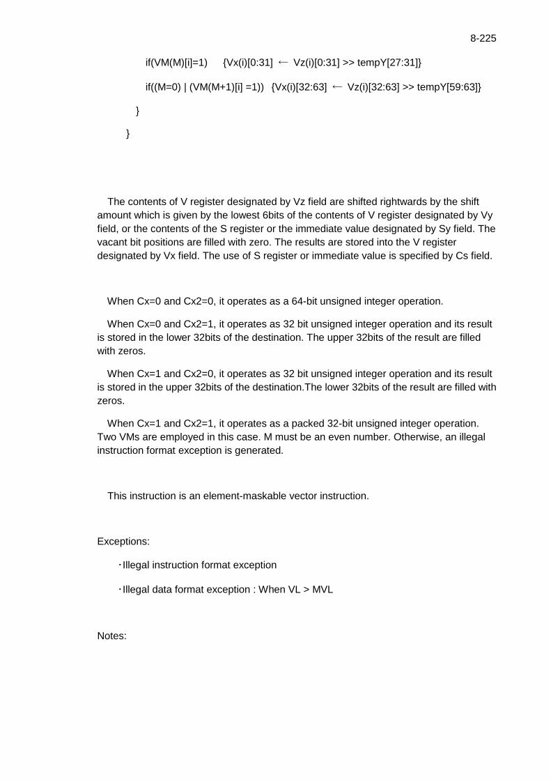
8-225
if(VM(M)[i]=1) {Vx(i)[0:31] ← Vz(i)[0:31] >> tempY[27:31]}
if((M=0) | (VM(M+1)[i] =1)) {Vx(i)[32:63] ← Vz(i)[32:63] >> tempY[59:63]}
}
}
The contents of V register designated by Vz field are shifted rightwards by the shift
amount which is given by the lowest 6bits of the contents of V register designated by Vy
field, or the contents of the S register or the immediate value designated by Sy field. The
vacant bit positions are filled with zero. The results are stored into the V register
designated by Vx field. The use of S register or immediate value is specified by Cs field.
When Cx=0 and Cx2=0, it operates as a 64-bit unsigned integer operation.
When Cx=0 and Cx2=1, it operates as 32 bit unsigned integer operation and its result
is stored in the lower 32bits of the destination. The upper 32bits of the result are filled
with zeros.
When Cx=1 and Cx2=0, it operates as 32 bit unsigned integer operation and its result
is stored in the upper 32bits of the destination.The lower 32bits of the result are filled with
zeros.
When Cx=1 and Cx2=1, it operates as a packed 32-bit unsigned integer operation.
Two VMs are employed in this case. M must be an even number. Otherwise, an illegal
instruction format exception is generated.
This instruction is an element-maskable vector instruction.
Exceptions:
・Illegal instruction format exception
・Illegal data format exception : When VL > MVL
Notes:
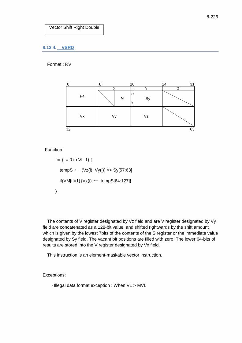
8-226
Vector Shift Right Double
8.12.4. VSRD
Format : RV
x
F4 Sy
y
C
y
z8 16 24 31
32 63
0
Vx Vy Vz
M
Function:
for (i = 0 to VL-1) {
tempS ← (Vz(i), Vy(i)) >> Sy[57:63]
if(VM[i]=1) {Vx(i) ← tempS[64:127]}
}
The contents of V register designated by Vz field and are V register designated by Vy
field are concatenated as a 128-bit value, and shifted rightwards by the shift amount
which is given by the lowest 7bits of the contents of the S register or the immediate value
designated by Sy field. The vacant bit positions are filled with zero. The lower 64-bits of
results are stored into the V register designated by Vx field.
This instruction is an element-maskable vector instruction.
Exceptions:
・Illegal data format exception : When VL > MVL
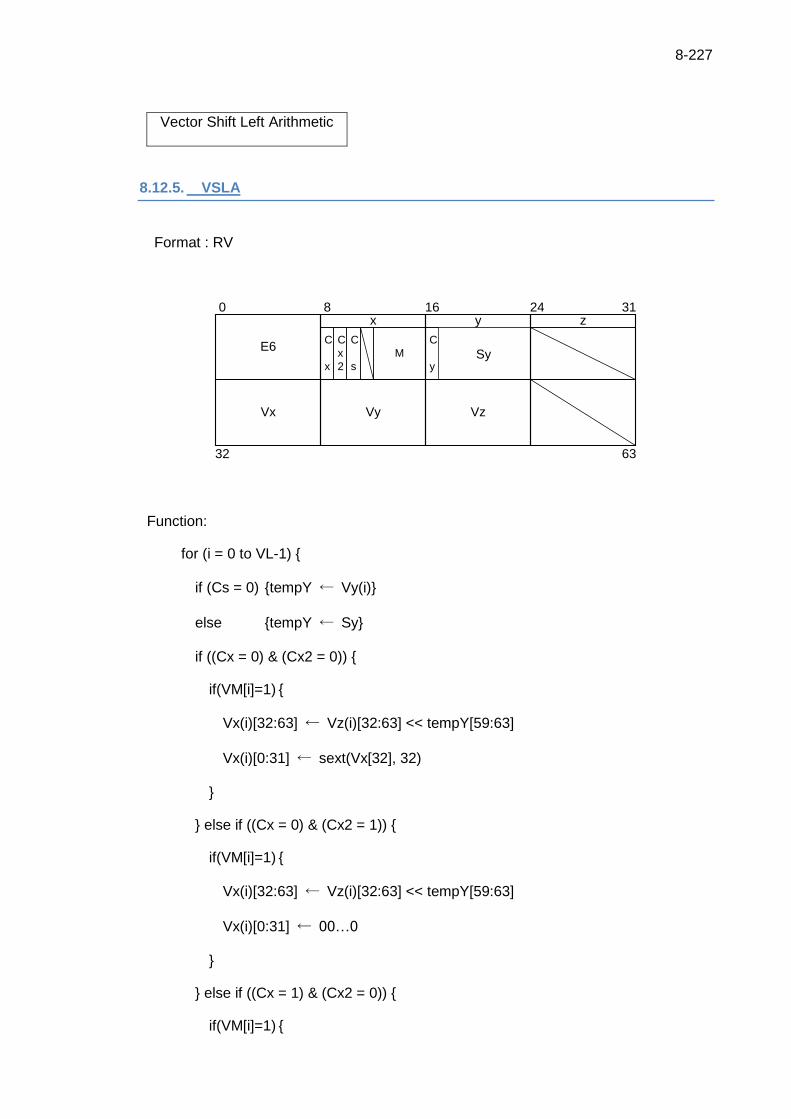
8-227
Vector Shift Left Arithmetic
8.12.5. VSLA
Format : RV
x
E6 Sy
y
C
y
z8 16 24 31
32 63
0
C
x
Vx Vy Vz
M
C
s
C
x
2
Function:
for (i = 0 to VL-1) {
if (Cs = 0) {tempY ← Vy(i)}
else {tempY ← Sy}
if ((Cx = 0) & (Cx2 = 0)) {
if(VM[i]=1) {
Vx(i)[32:63] ← Vz(i)[32:63] << tempY[59:63]
Vx(i)[0:31] ← sext(Vx[32], 32)
}
} else if ((Cx = 0) & (Cx2 = 1)) {
if(VM[i]=1) {
Vx(i)[32:63] ← Vz(i)[32:63] << tempY[59:63]
Vx(i)[0:31] ← 00…0
}
} else if ((Cx = 1) & (Cx2 = 0)) {
if(VM[i]=1) {
8-228
Vx(i)[0:31] ← Vz(i)[0:31] << tempY[27:31]
Vx(i)[32:63] ← 00…0
}
} else if ((Cx = 1) & (Cx2 = 1)) {
if(VM(M)[i]=1) {Vx(i)[0:31] ← Vz(i)[0:31] << tempY[27:31]}
if((M=0) | (VM(M+1)[i] =1)) {Vx(i)[32:63] ← Vz(i)[32:63] << tempY[59:63]}
}
}
The contents of V register designated by Vz field are shifted leftwards by the shift
amount which is given by the lowest 5bits of the contents of V register designated by Vy
field, or the contents of the S register or the immediate value designated by Sy field. The
vacant bit positions are filled with zero. The results are stored into the V register
designated by Vx field. The use of S register or immediate value is specified by Cs field.
When overflown a fixed-point overflow exception occurs.
When Cx=0 and Cx2=0, it operates as a 32-bit signed integer operation. The upper
32-bits of the result are filled with extended sign bits.
When Cx=0 and Cx2=1, it operates as 32 bit signed integer operation and its result is
stored in the lower 32bits of the destination. The upper 32bits of the result are filled with
zeros.
When Cx=1 and Cx2=0, it operates as 32 bit signed integer operation and its result is
stored in the upper 32bits of the destination.The lower 32bits of the result are filled with
zeros.
When Cx=1 and Cx2=1, it operates as a packed 32-bit signed integer operation. Two
VMs are employed in this case. M must be an even number. Otherwise, an illegal
instruction format exception is generated.
This instruction is an element-maskable vector instruction.
Exceptions:
・Illegal instruction format exception
・Fixed-point overflow exception
・Illegal data format exception : When VL > MVL
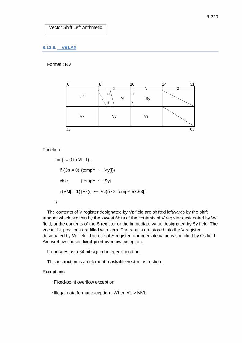
8-229
Vector Shift Left Arithmetic
8.12.6. VSLAX
Format : RV
x
D4 Sy
y
C
y
z8 16 24 31
32 63
0
Vx Vy Vz
M
C
s
Function :
for (i = 0 to VL-1) {
if (Cs = 0) {tempY ← Vy(i)}
else {tempY ← Sy}
if(VM[i]=1) {Vx(i) ← Vz(i) << tempY[58:63]}
}
The contents of V register designated by Vz field are shifted leftwards by the shift
amount which is given by the lowest 6bits of the contents of V register designated by Vy
field, or the contents of the S register or the immediate value designated by Sy field. The
vacant bit positions are filled with zero. The results are stored into the V register
designated by Vx field. The use of S register or immediate value is specified by Cs field.
An overflow causes fixed-point overflow exception.
It operates as a 64 bit signed integer operation.
This instruction is an element-maskable vector instruction.
Exceptions:
・Fixed-point overflow exception
・Illegal data format exception : When VL > MVL
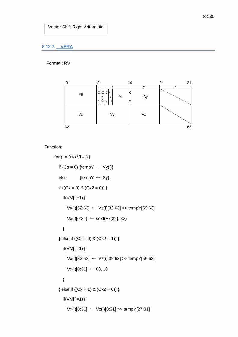
8-230
Vector Shift Right Arithmetic
8.12.7. VSRA
Format : RV
x
F6 Sy
y
C
y
z8 16 24 31
32 63
0
C
x
Vx Vy Vz
M
C
s
C
x
2
Function:
for (i = 0 to VL-1) {
if (Cs = 0) {tempY ← Vy(i)}
else {tempY ← Sy}
if ((Cx = 0) & (Cx2 = 0)) {
if(VM[i]=1) {
Vx(i)[32:63] ← Vz(i)[32:63] >> tempY[59:63]
Vx(i)[0:31] ← sext(Vx[32], 32)
}
} else if ((Cx = 0) & (Cx2 = 1)) {
if(VM[i]=1) {
Vx(i)[32:63] ← Vz(i)[32:63] >> tempY[59:63]
Vx(i)[0:31] ← 00…0
}
} else if ((Cx = 1) & (Cx2 = 0)) {
if(VM[i]=1) {
Vx(i)[0:31] ← Vz(i)[0:31] >> tempY[27:31]
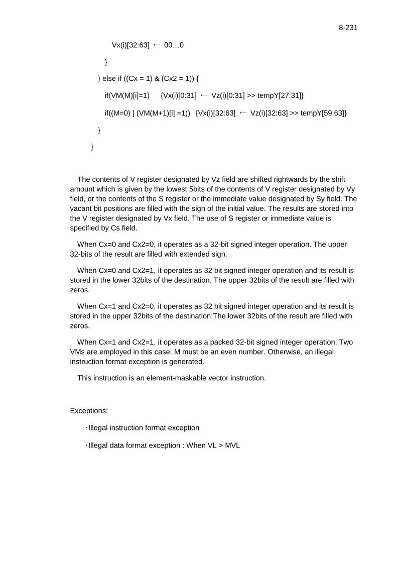
8-231
Vx(i)[32:63] ← 00…0
}
} else if ((Cx = 1) & (Cx2 = 1)) {
if(VM(M)[i]=1) {Vx(i)[0:31] ← Vz(i)[0:31] >> tempY[27:31]}
if((M=0) | (VM(M+1)[i] =1)) {Vx(i)[32:63] ← Vz(i)[32:63] >> tempY[59:63]}
}
}
The contents of V register designated by Vz field are shifted rightwards by the shift
amount which is given by the lowest 5bits of the contents of V register designated by Vy
field, or the contents of the S register or the immediate value designated by Sy field. The
vacant bit positions are filled with the sign of the initial value. The results are stored into
the V register designated by Vx field. The use of S register or immediate value is
specified by Cs field.
When Cx=0 and Cx2=0, it operates as a 32-bit signed integer operation. The upper
32-bits of the result are filled with extended sign.
When Cx=0 and Cx2=1, it operates as 32 bit signed integer operation and its result is
stored in the lower 32bits of the destination. The upper 32bits of the result are filled with
zeros.
When Cx=1 and Cx2=0, it operates as 32 bit signed integer operation and its result is
stored in the upper 32bits of the destination.The lower 32bits of the result are filled with
zeros.
When Cx=1 and Cx2=1, it operates as a packed 32-bit signed integer operation. Two
VMs are employed in this case. M must be an even number. Otherwise, an illegal
instruction format exception is generated.
This instruction is an element-maskable vector instruction.
Exceptions:
・Illegal instruction format exception
・Illegal data format exception : When VL > MVL
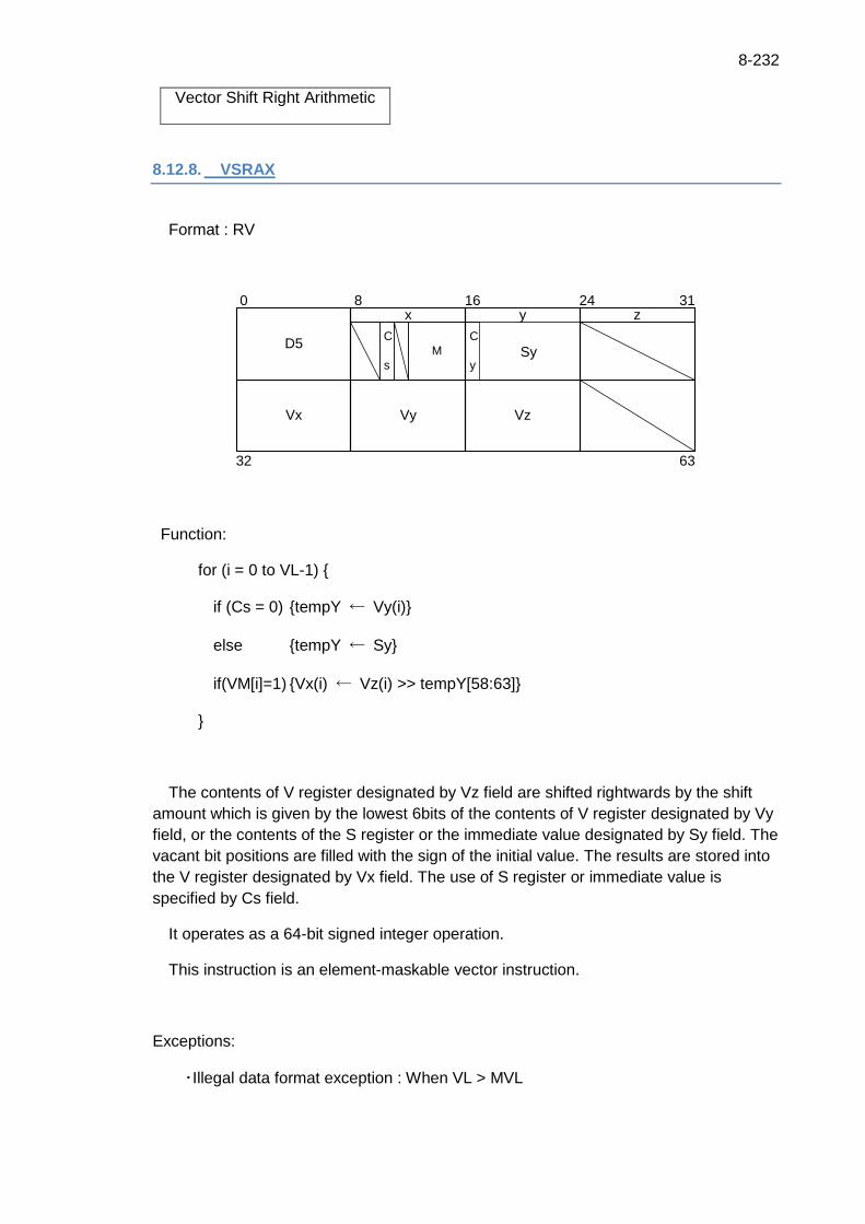
8-232
Vector Shift Right Arithmetic
8.12.8. VSRAX
Format : RV
x
D5 Sy
y
C
y
z8 16 24 31
32 63
0
Vx Vy Vz
M
C
s
Function:
for (i = 0 to VL-1) {
if (Cs = 0) {tempY ← Vy(i)}
else {tempY ← Sy}
if(VM[i]=1) {Vx(i) ← Vz(i) >> tempY[58:63]}
}
The contents of V register designated by Vz field are shifted rightwards by the shift
amount which is given by the lowest 6bits of the contents of V register designated by Vy
field, or the contents of the S register or the immediate value designated by Sy field. The
vacant bit positions are filled with the sign of the initial value. The results are stored into
the V register designated by Vx field. The use of S register or immediate value is
specified by Cs field.
It operates as a 64-bit signed integer operation.
This instruction is an element-maskable vector instruction.
Exceptions:
・Illegal data format exception : When VL > MVL
8-233
Vector Shift Left and Add
8.12.9. VSFA
Format : RV
x
D7 Sy
y
C
y
z8 16 24 31
32 63
0
Vx Vz
M SzC
z
Function:
for (i = 0 to VL-1) {
if(VM[i]=1) {Vx(i) ← Sz(i) + (Vz(i) << Sy[61:63])}
}
The contents of V register designated by Vz field are shifted left by the shift amount
which is given by the lowest 3bits of the contents of the S register or the immediate value
designated by Sy field, and added to the contents of the S register or the immediate
value designated by Sz field. The vacant bit positions are filled with zero. The results are
stored into the V register designated by Vx field. The use of S register or immediate value
is specified by Cs field.
It operates as a 64-bit unsigned integer operation.
This instruction is an element-maskable vector instruction.
Exceptions:
・Illegal data format exception : When VL > MVL
Notes:
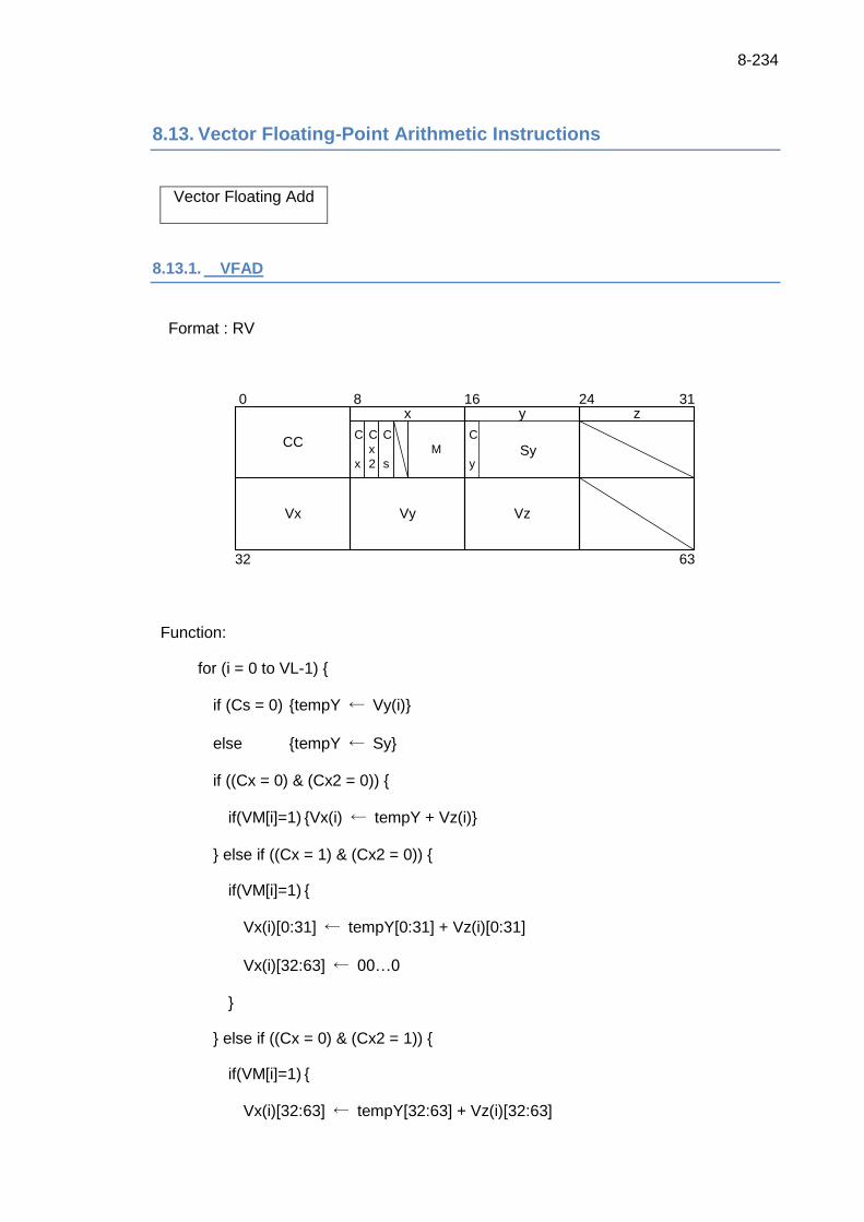
8-234
8.13. Vector Floating-Point Arithmetic Instructions
Vector Floating Add
8.13.1. VFAD
Format : RV
x
CC Sy
y
C
y
z8 16 24 31
32 63
0
C
x
Vx Vy Vz
M
C
s
C
x
2
Function:
for (i = 0 to VL-1) {
if (Cs = 0) {tempY ← Vy(i)}
else {tempY ← Sy}
if ((Cx = 0) & (Cx2 = 0)) {
if(VM[i]=1) {Vx(i) ← tempY + Vz(i)}
} else if ((Cx = 1) & (Cx2 = 0)) {
if(VM[i]=1) {
Vx(i)[0:31] ← tempY[0:31] + Vz(i)[0:31]
Vx(i)[32:63] ← 00…0
}
} else if ((Cx = 0) & (Cx2 = 1)) {
if(VM[i]=1) {
Vx(i)[32:63] ← tempY[32:63] + Vz(i)[32:63]
8-235
Vx(i)[0:31] ← 00…0
}
} else if ((Cx = 1) & (Cx2 = 1)) {
if(VM(M)[i]=1) {Vx(i)[0:31] ← tempY[0:31] + Vz(i)[0:31]}
if((M=0) | (VM(M+1)[i] =1)) {Vx(i)[32:63] ← tempY[32:63] + Vz(i)[32:63]}
}
}
The contents of the V register designated by Vy field, or the contents of the S register
or the immediate value designated by Sy field are added to the contents of the V register
designated by Vz field. The results are stored into the V register designated by Vx field.
The use of S register or immediate value is specified by Cs field.
When Cx=0 and Cx2=0, it operates as a double precision floating point operation.
When Cx=0 and Cx2=1, it operates as a 32 bit single precision floating point operation
and its result is stored in the lower 32bits of the destination. The upper 32bits of the result
are filled with zeros.
When Cx=1 and Cx2=0, it operates as a 32 bit single precision floating point operation
and its result is stored in the upper 32bits of the destination.The lower 32bits of the result
are filled with zeros.
When Cx=1 and Cx2=1, it operates as a packed single precision floating-point
operation. Two VMs are employed in this case. M must be an even number. Otherwise,
an illegal instruction format exception is generated.
This instruction is an element-maskable vector instruction.
Exceptions:
・Illegal instruction format exception
・Floating-point overflow exception
・Floating-point underflow exception
・Invalid operation exception
・Inexact exception
8-236
・Illegal data format exception : When VL > MVL
Notes:
・When (Cs=1) and (Cy=0)), y operand is the immediate value of signed integers( -64 ~
63).
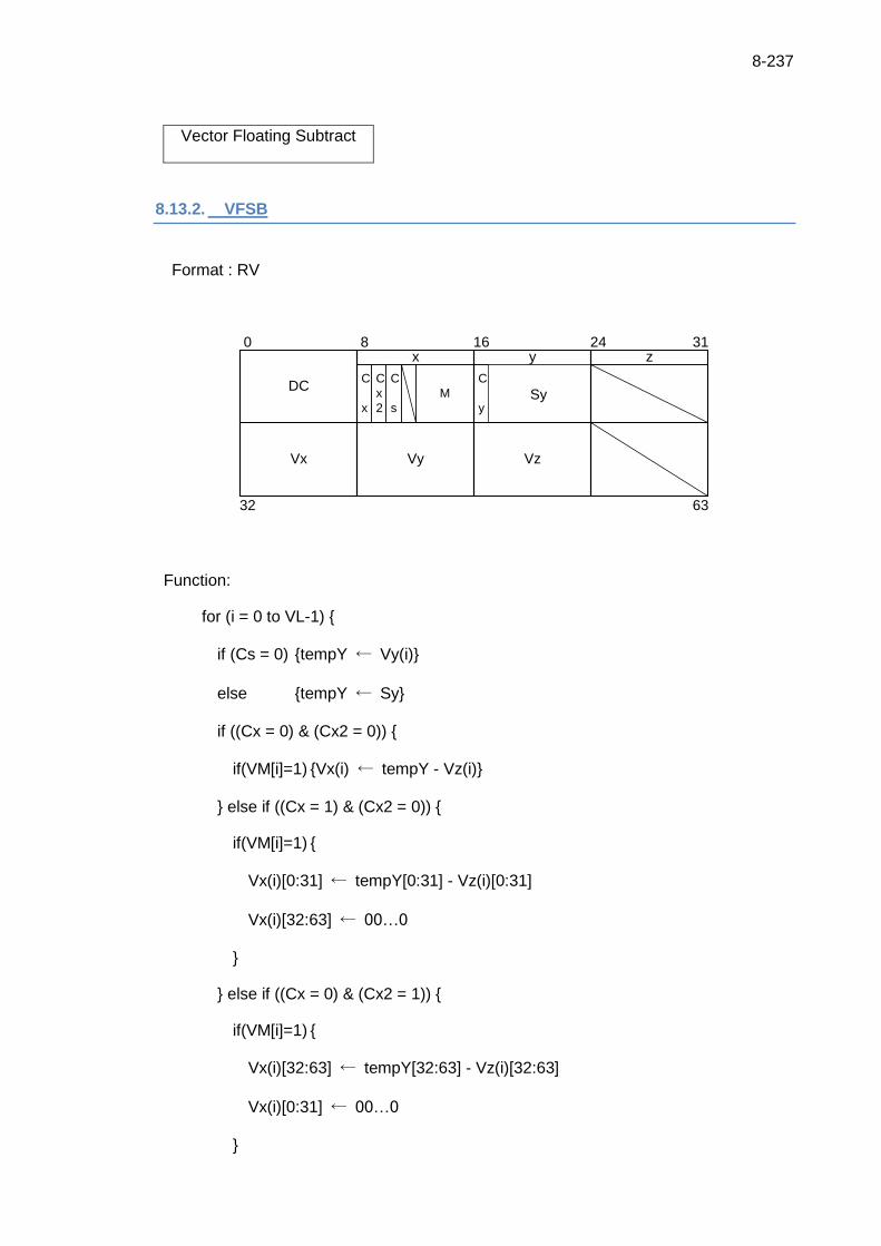
8-237
Vector Floating Subtract
8.13.2. VFSB
Format : RV
C
x
x
DC Sy
y
C
y
z8 16 24 31
32 63
0
Vx Vy Vz
M
C
s
C
x
2
Function:
for (i = 0 to VL-1) {
if (Cs = 0) {tempY ← Vy(i)}
else {tempY ← Sy}
if ((Cx = 0) & (Cx2 = 0)) {
if(VM[i]=1) {Vx(i) ← tempY - Vz(i)}
} else if ((Cx = 1) & (Cx2 = 0)) {
if(VM[i]=1) {
Vx(i)[0:31] ← tempY[0:31] - Vz(i)[0:31]
Vx(i)[32:63] ← 00…0
}
} else if ((Cx = 0) & (Cx2 = 1)) {
if(VM[i]=1) {
Vx(i)[32:63] ← tempY[32:63] - Vz(i)[32:63]
Vx(i)[0:31] ← 00…0
}

8-238
} else if ((Cx = 1) & (Cx2 = 1)) {
if(VM(M)[i]=1) {Vx(i)[0:31] ← tempY[0:31] - Vz(i)[0:31]}
if((M=0) | (VM(M+1)[i] =1)) {Vx(i)[32:63] ← tempY[32:63] - Vz(i)[32:63]}
}
}
The contents of V register designated by Vz field are subtracted from the contents of V
register designated by Vy field, or the contents of the S register or the immediate value
designated by Sy field. The results are stored into the V register designated by Vx field.
The use of S register or immediate value is specified by Cs field.
When Cx=0 and Cx2=0, it operates as a double precision floating-point operation.
When Cx=0 and Cx2=1, it operates as a 32 bit single precision floating point operation
and its result is stored in the lower 32bits of the destination. The upper 32bits of the result
are filled with zeros.
When Cx=1 and Cx2=0, it operates as a 32 bit single precision floating point operation
and its result is stored in the upper 32bits of the destination.The lower 32bits of the result
are filled with zeros.
When Cx=1 and Cx2=1, it operates as a packed single precision floating-point
operation. Two VMs are employed in this case. M must be an even number. Otherwise,
an illegal instruction format exception is generated.
This instruction is an element-maskable vector instruction.
Exceptions:
・Illegal instruction format exception
・Floating-point overflow exception
・Floating-point underflow exception
・Invalid operation exception
・Inexact exception
・Illegal data format exception : When VL > MVL

8-239
Notes:
・When (Cs=1) and (Cy=0)), y operand is the immediate value of signed integers( -64 ~
63).

8-240
Vector Floating Multiply
8.13.3. VFMP
Format : RV
x
CD Sy
y
C
y
z8 16 24 31
32 63
0
C
x
Vx Vy Vz
M
C
s
C
x
2
Function:
for (i = 0 to VL-1) {
if (Cs = 0) {tempY ← Vy(i)}
else {tempY ← Sy}
if ((Cx = 0) & (Cx2 = 0)) {
if(VM[i]=1) {Vx(i) ← tempY * Vz(i)}
} else if ((Cx = 1) & (Cx2 = 0)) {
if(VM[i]=1) {
Vx(i)[0:31] ← tempY[0:31] * Vz(i)[0:31]
Vx(i)[32:63] ← 00…0
}
} else if ((Cx = 0) & (Cx2 = 1)) {
if(VM[i]=1) {
Vx(i)[32:63] ← tempY[32:63] * Vz(i)[32:63]
Vx(i)[0:31] ← 00…0
}
8-241
} else if ((Cx = 1) & (Cx2 = 1)) {
if(VM(M)[i]=1) {Vx(i)[0:31] ← tempY[0:31] * Vz(i)[0:31]}
if((M=0) | (VM(M+1)[i] =1)) {Vx(i)[32:63] ← tempY[32:63] * Vz(i)[32:63]}
}
}
The contents of V register designated by Vz field are multiplied by the contents of V
register designated by Vy field, or the contents of the S register or the immediate value
designated by Sy field. The results are stored into the V register designated by Vx field.
The use of S register or immediate value is specified by Cs field.
When Cx=0 and Cx2=0, it operates as a double precision floating-point operation.
When Cx=0 and Cx2=1, it operates as a 32 bit single precision floating point operation
and its result is stored in the lower 32bits of the destination. The upper 32bits of the result
are filled with zeros.
When Cx=1 and Cx2=0, it operates as a 32 bit single precision floating point operation
and its result is stored in the upper 32bits of the destination.The lower 32bits of the result
are filled with zeros.
When Cx=1 and Cx2=1, it operates as a packed single precision floating-point
operation. Two VMs are employed in this case. M must be an even number. Otherwise,
an illegal instruction format exception is generated.
This instruction is an element-maskable vector instruction.
Exceptions:
・Illegal instruction format exception
・Floating-point overflow exception
・Floating-point underflow exception
・Invalid operation exception
・Inexact exception
・Illegal data format exception : When VL > MVL
8-242
Notes:
・When (Cs=1) and (Cy=0)), y operand is the immediate value of signed integers( -64 ~
63).
8-243
Vector Floating Divide
8.13.4. VFDV
Format : RV
x
DD Sy
y
C
y
z8 16 24 31
32 63
0
C
x
Vx Vy Vz
M
C
s
C
s
2
Function:
if ((Cs = 1) & (Cs2 = 1)) {illegal instruction format exception}
for (i = 0 to VL-1) {
if ((Cs = 0) & (Cs2 = 0)) {tempY ← Vy(i); tempZ ← Vz(i)}
else if ((Cs = 1) & (Cs2 = 0)) {tempY ← Sy; tempZ ← Vz(i)}
else if ((Cs = 0) & (Cs2 = 1)) {tempY ← Vy(i); tempZ ← Sy}
if (Cx = 0) {
if(VM[i]=1) {Vx(i) ← tempY / tempZ}
} else if (Cx = 1) {
if(VM[i]=1) {
Vx(i)[0:31] ← tempY[0:31] / tempZ[0:31]
Vx(i)[32:63] ← 00…0
}
}
}
8-244
The contents of V register designated by Vz field, or the contents of the S register or
the immediate value designated by Sy field are divided by the contents of V register
designated by Vy field, or the contents of the S register or the immediate value
designated by Sy field. The results are stored into the V register designated by Vx field.
The use of S register or immediate value is specified by Cs and Cs2 field.
When Cs=0 and Cs2=0, it divides Vy by Vz.
When Cs=1 and Cs2=0, it divides Sy by Vz.
When Cs=0 and Cs2=1, it divides Vy by Sy.
When Cs=1 and Cs2=1, illegal instruction format exception occurs.
When Cx=0, it operates as a double precision floating-point operation.
When Cx=1, it operates as a single precision floating-point operation. The lower 32-bits
of the result are filled with zero.
This instruction is an element-maskable vector instruction.
8-245
Exceptions:
・Divide exception
・Floating-point overflow exception
・Floating-point underflow exception
・Invalid operation exception
・Inexact exception
・Illegal instruction format exception
・Illegal data format exception : When VL > MVL
Notes:
・When (Cs=1) and (Cy=0)), y operand is the immediate value of signed integers( -64 ~
63).
8-246
Vector floating Square Root
8.13.5. VFSQRT
Format : RV
x
ED
y z8 16 24 31
32 63
0
C
x
Vx Vy
M
Function:
for (i = 0 to VL-1) {
if (Cx = 0) {
if(VM[i]=1) {Vx(i) ← Vy(i) }
} else {
if(VM[i]=1) {
Vx(i)[0:31] ← 31:0Vy(i)
Vx(i)[32:63] ← 00…0
}
}
}
Square root operation is performed using the contents of the V register designated by
the Vy field. The results are stored into the V register designated by Vx field.
8-247
When Cx=0, it operates as a double precision floating-point operation.
When Cx=1, it operates as a single precision floating-point operation. The lower 32-bits
of the result are filled with zero.
This instruction is an element-maskable vector instruction.
Exceptions:
・Invalid operation exception
・Inexact exception
・Illegal data format exception : When VL > MVL
Notes:

8-248
Vector Floating Compare
8.13.6. VFCP
Format : RV
x
FC Sy
y
C
y
z8 16 24 31
32 63
0
C
x
Vx Vy Vz
M
C
s
C
x
2
Function:
for (i = 0 to VL-1) {
if (Cs = 0) {tempY ← Vy(i)}
else {tempY ← Sy}
if ((Cx = 0) & (Cx2 = 0)) {
if(VM[i]=1) {Vx(i) ← compare(tempY, Vz(i))}
} else if ((Cx = 1) & (Cx2 = 0)) {
if(VM[i]=1) {
Vx(i)[0:31] ← compare(tempY[0:31], Vz(i)[0:31])
Vx(i)[32:63] ← 00…0
}
} else if ((Cx = 0) & (Cx2 = 1)) {
if(VM[i]=1) {
Vx(i)[32:63] ← compare(tempY[32:63], Vz(i)[32:63])
Vx(i)[0:31] ← 00…0
}
8-249
} else if ((Cx = 1) & (Cx2 = 1)) {
if(VM(M)[i]=1) {Vx(i)[0:31] ← compare(tempY[0:31], Vz(i)[0:31])}
if((M=0) | (VM(M+1)[i] =1)) {Vx(i)[32:63] ← compare(tempY[32:63],
Vz(i)[32:63])}
}
}
where compare(y, z) is defined as follows.
compare(y, z) {
if (y > z) {x ← positive nonzero value}
else if (y = z) {x ← 00…0}
else if (y < z) {x ← negative nonzero value}
else {x ← quiet NaN}
return x
}
The contents of the V register designated by Vy field, or the contents of the S register
or the immediate value designated by Sy field are compared with the contents of the V
register designated by Vz field. The results are stored into the V register designated by
Vx field. The use of S register or immediate value is specified by Cs field.
When Cx=0 and Cx2=0, it operates as a double precision floating-point operation.
When Cx=0 and Cx2=1, it operates as a 32 bit single precision floating point operation
and its result is stored in the lower 32bits of the destination. The upper 32bits of the result
are filled with zeros.
When Cx=1 and Cx2=0, it operates as a 32 bit single precision floating point operation
and its result is stored in the upper 32bits of the destination.The lower 32bits of the result
are filled with zeros.
When Cx=1 and Cx2=1, it operates as a packed single precision floating-point
operation. Two VMs are employed in this case. M must be an even number. Otherwise,
an illegal instruction format exception is generated.
8-250
This instruction is an element-maskable vector instruction.
Exceptions:
・Illegal instruction format exception
・Invalid operation exception
・Illegal data format exception : When VL > MVL
Notes:
・When (Cs=1) and (Cy=0)), y operand is the immediate value of signed integers( -64 ~
63).
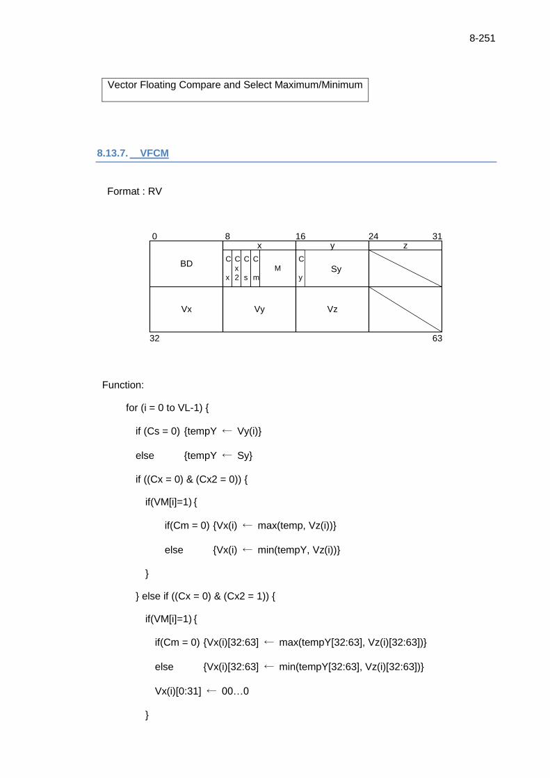
8-251
Vector Floating Compare and Select Maximum/Minimum
8.13.7. VFCM
Format : RV
x
BD Sy
y
C
y
z8 16 24 31
32 63
0
C
x
Vx Vy Vz
M
C
s
C
m
C
x
2
Function:
for (i = 0 to VL-1) {
if (Cs = 0) {tempY ← Vy(i)}
else {tempY ← Sy}
if ((Cx = 0) & (Cx2 = 0)) {
if(VM[i]=1) {
if(Cm = 0) {Vx(i) ← max(temp, Vz(i))}
else {Vx(i) ← min(tempY, Vz(i))}
}
} else if ((Cx = 0) & (Cx2 = 1)) {
if(VM[i]=1) {
if(Cm = 0) {Vx(i)[32:63] ← max(tempY[32:63], Vz(i)[32:63])}
else {Vx(i)[32:63] ← min(tempY[32:63], Vz(i)[32:63])}
Vx(i)[0:31] ← 00…0
}
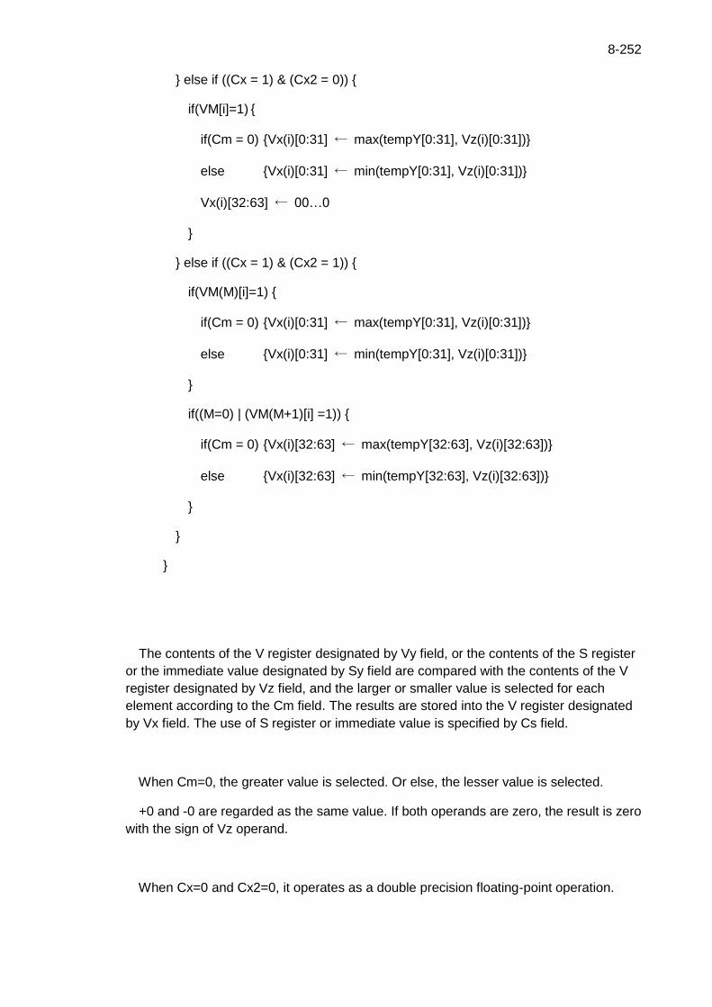
8-252
} else if ((Cx = 1) & (Cx2 = 0)) {
if(VM[i]=1) {
if(Cm = 0) {Vx(i)[0:31] ← max(tempY[0:31], Vz(i)[0:31])}
else {Vx(i)[0:31] ← min(tempY[0:31], Vz(i)[0:31])}
Vx(i)[32:63] ← 00…0
}
} else if ((Cx = 1) & (Cx2 = 1)) {
if(VM(M)[i]=1) {
if(Cm = 0) {Vx(i)[0:31] ← max(tempY[0:31], Vz(i)[0:31])}
else {Vx(i)[0:31] ← min(tempY[0:31], Vz(i)[0:31])}
}
if((M=0) | (VM(M+1)[i] =1)) {
if(Cm = 0) {Vx(i)[32:63] ← max(tempY[32:63], Vz(i)[32:63])}
else {Vx(i)[32:63] ← min(tempY[32:63], Vz(i)[32:63])}
}
}
}
The contents of the V register designated by Vy field, or the contents of the S register
or the immediate value designated by Sy field are compared with the contents of the V
register designated by Vz field, and the larger or smaller value is selected for each
element according to the Cm field. The results are stored into the V register designated
by Vx field. The use of S register or immediate value is specified by Cs field.
When Cm=0, the greater value is selected. Or else, the lesser value is selected.
+0 and -0 are regarded as the same value. If both operands are zero, the result is zero
with the sign of Vz operand.
When Cx=0 and Cx2=0, it operates as a double precision floating-point operation.
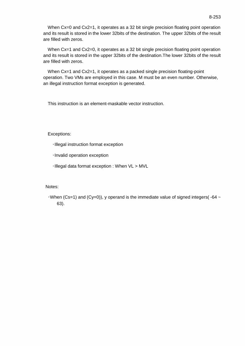
8-253
When Cx=0 and Cx2=1, it operates as a 32 bit single precision floating point operation
and its result is stored in the lower 32bits of the destination. The upper 32bits of the result
are filled with zeros.
When Cx=1 and Cx2=0, it operates as a 32 bit single precision floating point operation
and its result is stored in the upper 32bits of the destination.The lower 32bits of the result
are filled with zeros.
When Cx=1 and Cx2=1, it operates as a packed single precision floating-point
operation. Two VMs are employed in this case. M must be an even number. Otherwise,
an illegal instruction format exception is generated.
This instruction is an element-maskable vector instruction.
Exceptions:
・Illegal instruction format exception
・Invalid operation exception
・Illegal data format exception : When VL > MVL
Notes:
・When (Cs=1) and (Cy=0)), y operand is the immediate value of signed integers( -64 ~
63).
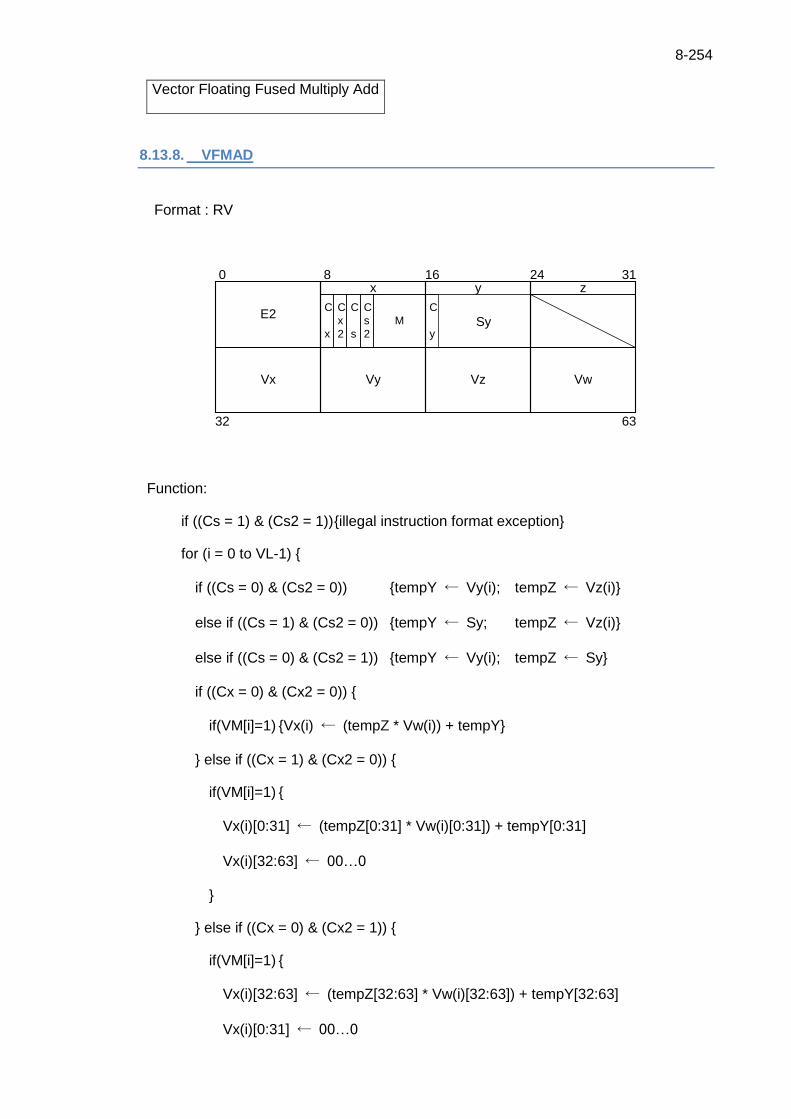
8-254
Vector Floating Fused Multiply Add
8.13.8. VFMAD
Format : RV
x
E2 Sy
y
C
y
z8 16 24 31
32 63
0
C
x
Vx Vy Vz Vw
M
C
s
C
s
2
C
x
2
Function:
if ((Cs = 1) & (Cs2 = 1)) {illegal instruction format exception}
for (i = 0 to VL-1) {
if ((Cs = 0) & (Cs2 = 0)) {tempY ← Vy(i); tempZ ← Vz(i)}
else if ((Cs = 1) & (Cs2 = 0)) {tempY ← Sy; tempZ ← Vz(i)}
else if ((Cs = 0) & (Cs2 = 1)) {tempY ← Vy(i); tempZ ← Sy}
if ((Cx = 0) & (Cx2 = 0)) {
if(VM[i]=1) {Vx(i) ← (tempZ * Vw(i)) + tempY}
} else if ((Cx = 1) & (Cx2 = 0)) {
if(VM[i]=1) {
Vx(i)[0:31] ← (tempZ[0:31] * Vw(i)[0:31]) + tempY[0:31]
Vx(i)[32:63] ← 00…0
}
} else if ((Cx = 0) & (Cx2 = 1)) {
if(VM[i]=1) {
Vx(i)[32:63] ← (tempZ[32:63] * Vw(i)[32:63]) + tempY[32:63]
Vx(i)[0:31] ← 00…0
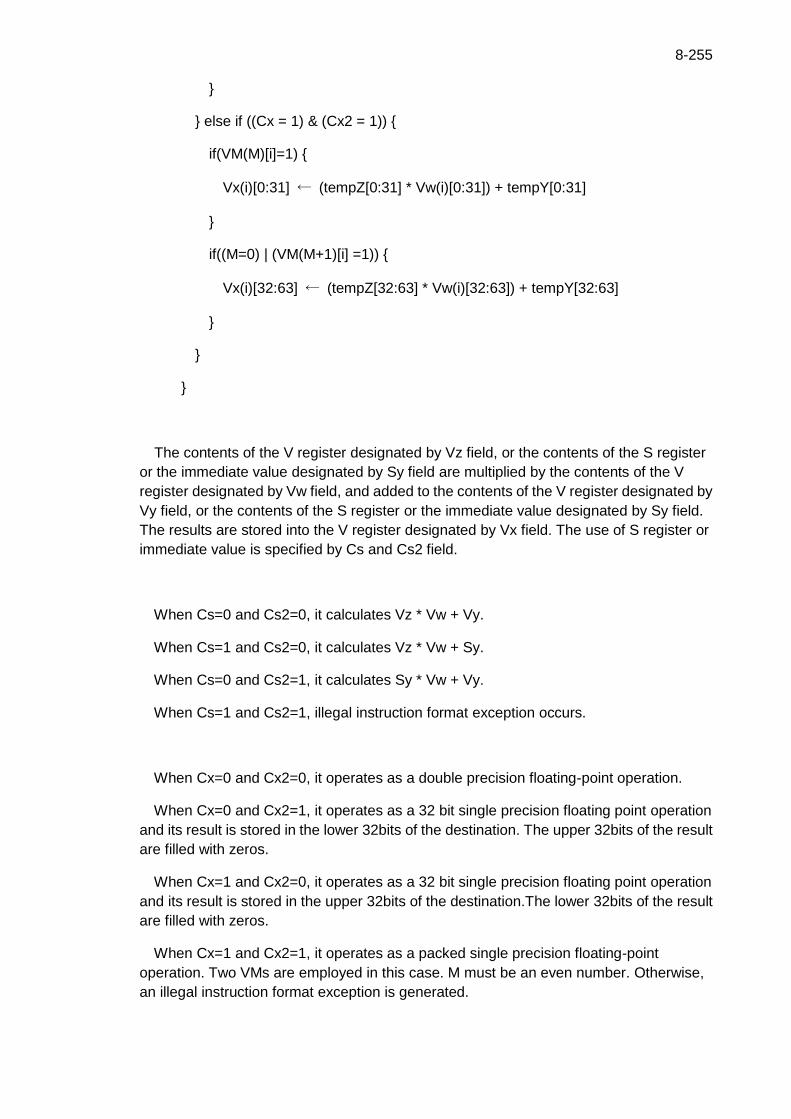
8-255
}
} else if ((Cx = 1) & (Cx2 = 1)) {
if(VM(M)[i]=1) {
Vx(i)[0:31] ← (tempZ[0:31] * Vw(i)[0:31]) + tempY[0:31]
}
if((M=0) | (VM(M+1)[i] =1)) {
Vx(i)[32:63] ← (tempZ[32:63] * Vw(i)[32:63]) + tempY[32:63]
}
}
}
The contents of the V register designated by Vz field, or the contents of the S register
or the immediate value designated by Sy field are multiplied by the contents of the V
register designated by Vw field, and added to the contents of the V register designated by
Vy field, or the contents of the S register or the immediate value designated by Sy field.
The results are stored into the V register designated by Vx field. The use of S register or
immediate value is specified by Cs and Cs2 field.
When Cs=0 and Cs2=0, it calculates Vz * Vw + Vy.
When Cs=1 and Cs2=0, it calculates Vz * Vw + Sy.
When Cs=0 and Cs2=1, it calculates Sy * Vw + Vy.
When Cs=1 and Cs2=1, illegal instruction format exception occurs.
When Cx=0 and Cx2=0, it operates as a double precision floating-point operation.
When Cx=0 and Cx2=1, it operates as a 32 bit single precision floating point operation
and its result is stored in the lower 32bits of the destination. The upper 32bits of the result
are filled with zeros.
When Cx=1 and Cx2=0, it operates as a 32 bit single precision floating point operation
and its result is stored in the upper 32bits of the destination.The lower 32bits of the result
are filled with zeros.
When Cx=1 and Cx2=1, it operates as a packed single precision floating-point
operation. Two VMs are employed in this case. M must be an even number. Otherwise,
an illegal instruction format exception is generated.
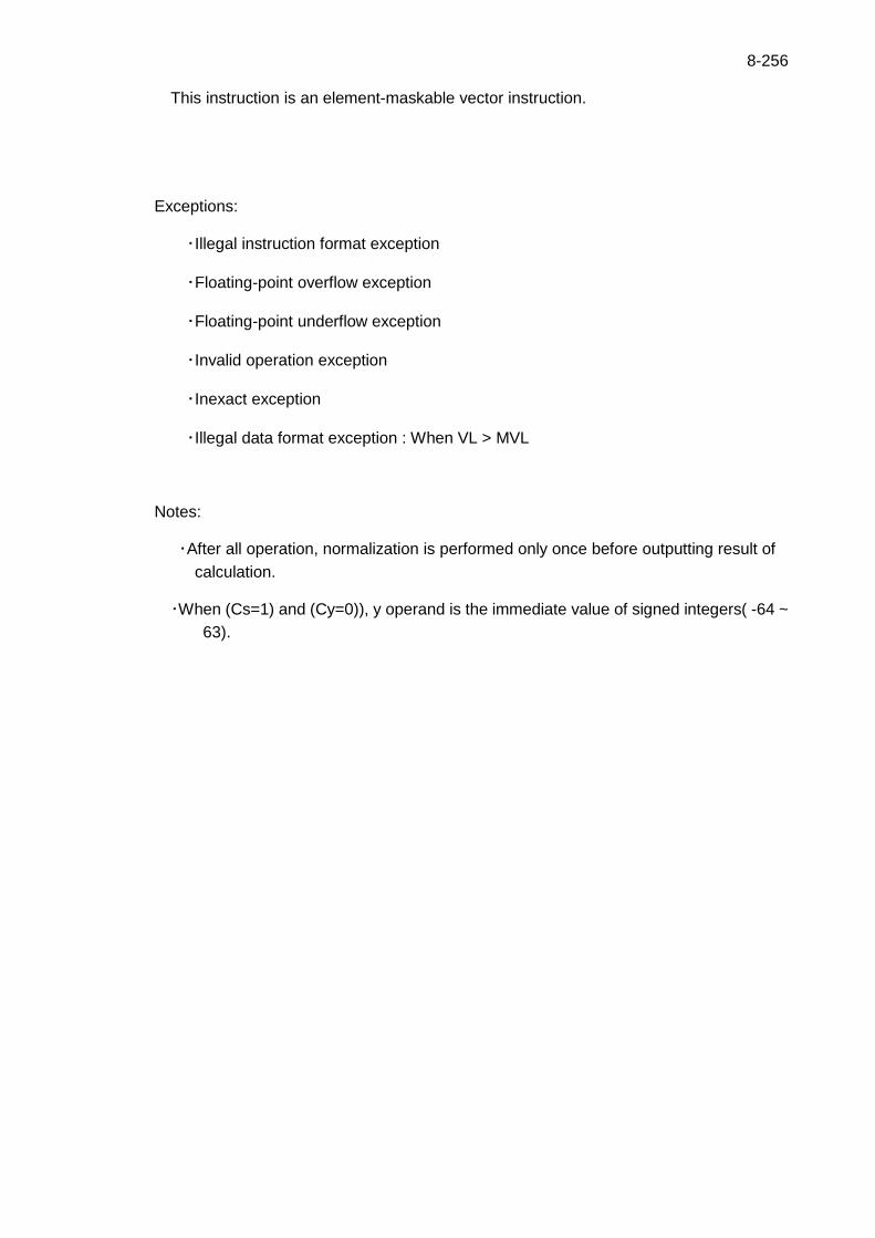
8-256
This instruction is an element-maskable vector instruction.
Exceptions:
・Illegal instruction format exception
・Floating-point overflow exception
・Floating-point underflow exception
・Invalid operation exception
・Inexact exception
・Illegal data format exception : When VL > MVL
Notes:
・After all operation, normalization is performed only once before outputting result of
calculation.
・When (Cs=1) and (Cy=0)), y operand is the immediate value of signed integers( -64 ~
63).
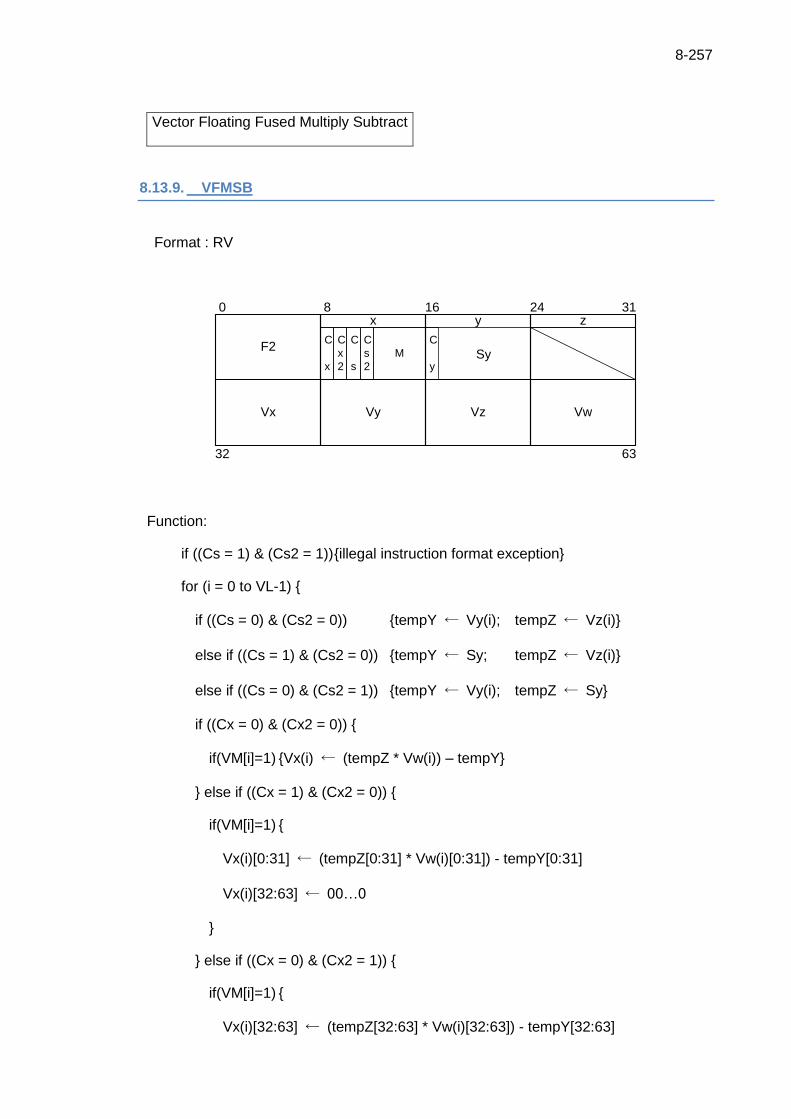
8-257
Vector Floating Fused Multiply Subtract
8.13.9. VFMSB
Format : RV
x
F2 Sy
y
C
y
z8 16 24 31
32 63
0
C
x
Vx Vy Vz Vw
M
C
s
C
s
2
C
x
2
Function:
if ((Cs = 1) & (Cs2 = 1)) {illegal instruction format exception}
for (i = 0 to VL-1) {
if ((Cs = 0) & (Cs2 = 0)) {tempY ← Vy(i); tempZ ← Vz(i)}
else if ((Cs = 1) & (Cs2 = 0)) {tempY ← Sy; tempZ ← Vz(i)}
else if ((Cs = 0) & (Cs2 = 1)) {tempY ← Vy(i); tempZ ← Sy}
if ((Cx = 0) & (Cx2 = 0)) {
if(VM[i]=1) {Vx(i) ← (tempZ * Vw(i)) – tempY}
} else if ((Cx = 1) & (Cx2 = 0)) {
if(VM[i]=1) {
Vx(i)[0:31] ← (tempZ[0:31] * Vw(i)[0:31]) - tempY[0:31]
Vx(i)[32:63] ← 00…0
}
} else if ((Cx = 0) & (Cx2 = 1)) {
if(VM[i]=1) {
Vx(i)[32:63] ← (tempZ[32:63] * Vw(i)[32:63]) - tempY[32:63]
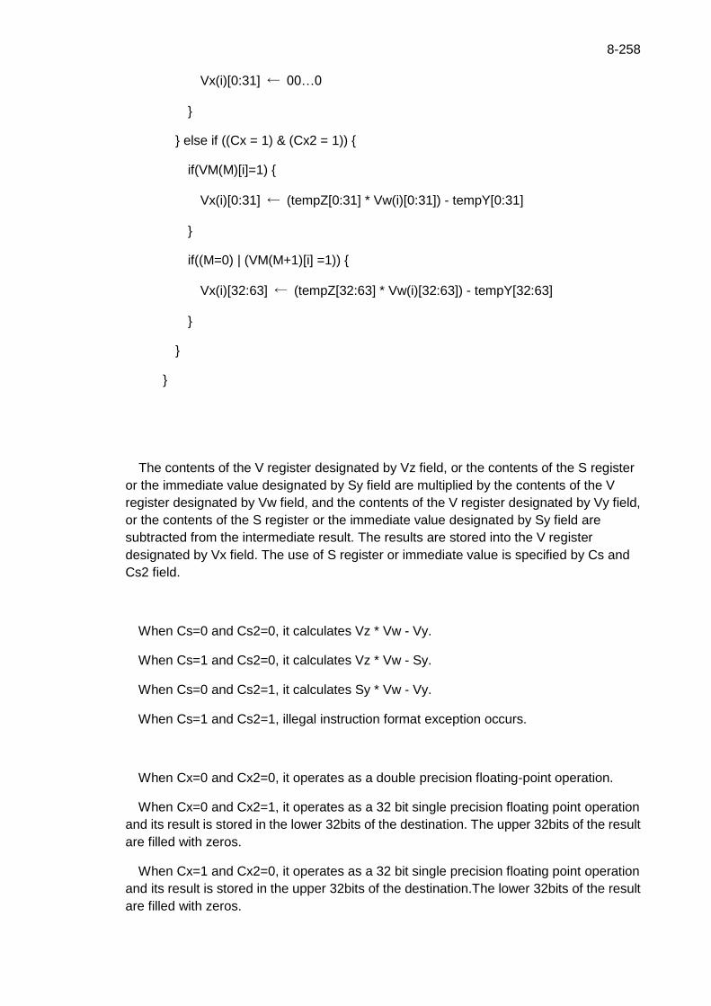
8-258
Vx(i)[0:31] ← 00…0
}
} else if ((Cx = 1) & (Cx2 = 1)) {
if(VM(M)[i]=1) {
Vx(i)[0:31] ← (tempZ[0:31] * Vw(i)[0:31]) - tempY[0:31]
}
if((M=0) | (VM(M+1)[i] =1)) {
Vx(i)[32:63] ← (tempZ[32:63] * Vw(i)[32:63]) - tempY[32:63]
}
}
}
The contents of the V register designated by Vz field, or the contents of the S register
or the immediate value designated by Sy field are multiplied by the contents of the V
register designated by Vw field, and the contents of the V register designated by Vy field,
or the contents of the S register or the immediate value designated by Sy field are
subtracted from the intermediate result. The results are stored into the V register
designated by Vx field. The use of S register or immediate value is specified by Cs and
Cs2 field.
When Cs=0 and Cs2=0, it calculates Vz * Vw - Vy.
When Cs=1 and Cs2=0, it calculates Vz * Vw - Sy.
When Cs=0 and Cs2=1, it calculates Sy * Vw - Vy.
When Cs=1 and Cs2=1, illegal instruction format exception occurs.
When Cx=0 and Cx2=0, it operates as a double precision floating-point operation.
When Cx=0 and Cx2=1, it operates as a 32 bit single precision floating point operation
and its result is stored in the lower 32bits of the destination. The upper 32bits of the result
are filled with zeros.
When Cx=1 and Cx2=0, it operates as a 32 bit single precision floating point operation
and its result is stored in the upper 32bits of the destination.The lower 32bits of the result
are filled with zeros.
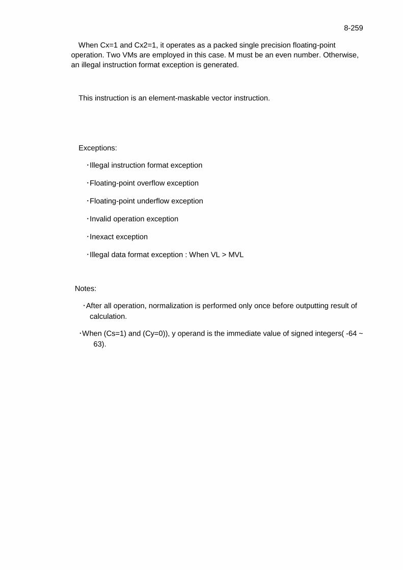
8-259
When Cx=1 and Cx2=1, it operates as a packed single precision floating-point
operation. Two VMs are employed in this case. M must be an even number. Otherwise,
an illegal instruction format exception is generated.
This instruction is an element-maskable vector instruction.
Exceptions:
・Illegal instruction format exception
・Floating-point overflow exception
・Floating-point underflow exception
・Invalid operation exception
・Inexact exception
・Illegal data format exception : When VL > MVL
Notes:
・After all operation, normalization is performed only once before outputting result of
calculation.
・When (Cs=1) and (Cy=0)), y operand is the immediate value of signed integers( -64 ~
63).
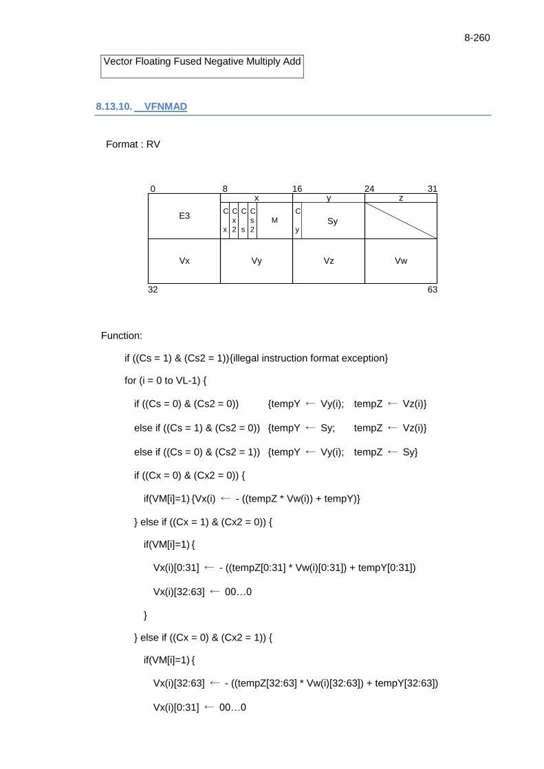
8-260
Vector Floating Fused Negative Multiply Add
8.13.10. VFNMAD
Format : RV
x
E3 Sy
y
C
y
z8 16 24 31
32 63
0
C
x
Vx Vy Vz Vw
M
C
s
C
s
2
C
x
2
Function:
if ((Cs = 1) & (Cs2 = 1)) {illegal instruction format exception}
for (i = 0 to VL-1) {
if ((Cs = 0) & (Cs2 = 0)) {tempY ← Vy(i); tempZ ← Vz(i)}
else if ((Cs = 1) & (Cs2 = 0)) {tempY ← Sy; tempZ ← Vz(i)}
else if ((Cs = 0) & (Cs2 = 1)) {tempY ← Vy(i); tempZ ← Sy}
if ((Cx = 0) & (Cx2 = 0)) {
if(VM[i]=1) {Vx(i) ← - ((tempZ * Vw(i)) + tempY)}
} else if ((Cx = 1) & (Cx2 = 0)) {
if(VM[i]=1) {
Vx(i)[0:31] ← - ((tempZ[0:31] * Vw(i)[0:31]) + tempY[0:31])
Vx(i)[32:63] ← 00…0
}
} else if ((Cx = 0) & (Cx2 = 1)) {
if(VM[i]=1) {
Vx(i)[32:63] ← - ((tempZ[32:63] * Vw(i)[32:63]) + tempY[32:63])
Vx(i)[0:31] ← 00…0
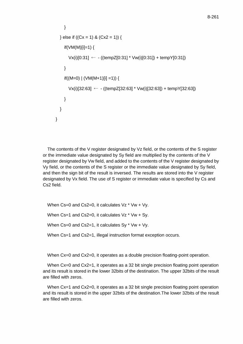
8-261
}
} else if ((Cx = 1) & (Cx2 = 1)) {
if(VM(M)[i]=1) {
Vx(i)[0:31] ← - ((tempZ[0:31] * Vw(i)[0:31]) + tempY[0:31])
}
if((M=0) | (VM(M+1)[i] =1)) {
Vx(i)[32:63] ← - ((tempZ[32:63] * Vw(i)[32:63]) + tempY[32:63])
}
}
}
The contents of the V register designated by Vz field, or the contents of the S register
or the immediate value designated by Sy field are multiplied by the contents of the V
register designated by Vw field, and added to the contents of the V register designated by
Vy field, or the contents of the S register or the immediate value designated by Sy field,
and then the sign bit of the result is inversed. The results are stored into the V register
designated by Vx field. The use of S register or immediate value is specified by Cs and
Cs2 field.
When Cs=0 and Cs2=0, it calculates Vz * Vw + Vy.
When Cs=1 and Cs2=0, it calculates Vz * Vw + Sy.
When Cs=0 and Cs2=1, it calculates Sy * Vw + Vy.
When Cs=1 and Cs2=1, illegal instruction format exception occurs.
When Cx=0 and Cx2=0, it operates as a double precision floating-point operation.
When Cx=0 and Cx2=1, it operates as a 32 bit single precision floating point operation
and its result is stored in the lower 32bits of the destination. The upper 32bits of the result
are filled with zeros.
When Cx=1 and Cx2=0, it operates as a 32 bit single precision floating point operation
and its result is stored in the upper 32bits of the destination.The lower 32bits of the result
are filled with zeros.
8-262
When Cx=1 and Cx2=1, it operates as a packed single precision floating-point
operation. Two VMs are employed in this case. M must be an even number. Otherwise,
an illegal instruction format exception is generated.
This instruction is an element-maskable vector instruction.
Exceptions:
・Illegal instruction format exception
・Floating-point overflow exception
・Floating-point underflow exception
・Invalid operation exception
・Inexact exception
・Illegal data format exception : When VL > MVL
Notes:
・After all operation, normalization is performed only once before outputting result of
calculation.
・When (Cs=1) and (Cy=0)), y operand is the immediate value of signed integers( -64 ~
63).
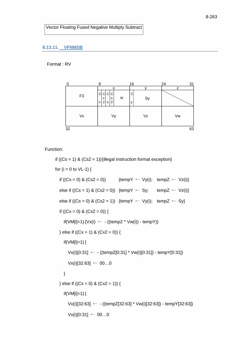
8-263
Vector Floating Fused Negative Multiply Subtract
8.13.11. VFNMSB
Format : RV
x
F3 Sy
y
C
y
z8 16 24 31
32 63
0
C
x
Vx Vy Vz Vw
M
C
s
C
s
2
C
x
2
Function:
if ((Cs = 1) & (Cs2 = 1)) {illegal instruction format exception}
for (i = 0 to VL-1) {
if ((Cs = 0) & (Cs2 = 0)) {tempY ← Vy(i); tempZ ← Vz(i)}
else if ((Cs = 1) & (Cs2 = 0)) {tempY ← Sy; tempZ ← Vz(i)}
else if ((Cs = 0) & (Cs2 = 1)) {tempY ← Vy(i); tempZ ← Sy}
if ((Cx = 0) & (Cx2 = 0)) {
if(VM[i]=1) {Vx(i) ← - ((tempZ * Vw(i)) - tempY)}
} else if ((Cx = 1) & (Cx2 = 0)) {
if(VM[i]=1) {
Vx(i)[0:31] ← - ((tempZ[0:31] * Vw(i)[0:31]) - tempY[0:31])
Vx(i)[32:63] ← 00…0
}
} else if ((Cx = 0) & (Cx2 = 1)) {
if(VM[i]=1) {
Vx(i)[32:63] ← - ((tempZ[32:63] * Vw(i)[32:63]) - tempY[32:63])
Vx(i)[0:31] ← 00…0
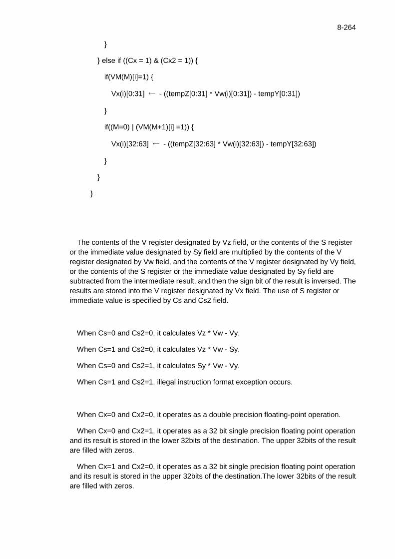
8-264
}
} else if ((Cx = 1) & (Cx2 = 1)) {
if(VM(M)[i]=1) {
Vx(i)[0:31] ← - ((tempZ[0:31] * Vw(i)[0:31]) - tempY[0:31])
}
if((M=0) | (VM(M+1)[i] =1)) {
Vx(i)[32:63] ← - ((tempZ[32:63] * Vw(i)[32:63]) - tempY[32:63])
}
}
}
The contents of the V register designated by Vz field, or the contents of the S register
or the immediate value designated by Sy field are multiplied by the contents of the V
register designated by Vw field, and the contents of the V register designated by Vy field,
or the contents of the S register or the immediate value designated by Sy field are
subtracted from the intermediate result, and then the sign bit of the result is inversed. The
results are stored into the V register designated by Vx field. The use of S register or
immediate value is specified by Cs and Cs2 field.
When Cs=0 and Cs2=0, it calculates Vz * Vw - Vy.
When Cs=1 and Cs2=0, it calculates Vz * Vw - Sy.
When Cs=0 and Cs2=1, it calculates Sy * Vw - Vy.
When Cs=1 and Cs2=1, illegal instruction format exception occurs.
When Cx=0 and Cx2=0, it operates as a double precision floating-point operation.
When Cx=0 and Cx2=1, it operates as a 32 bit single precision floating point operation
and its result is stored in the lower 32bits of the destination. The upper 32bits of the result
are filled with zeros.
When Cx=1 and Cx2=0, it operates as a 32 bit single precision floating point operation
and its result is stored in the upper 32bits of the destination.The lower 32bits of the result
are filled with zeros.
8-265
When Cx=1 and Cx2=1, it operates as a packed single precision floating-point
operation. Two VMs are employed in this case. M must be an even number. Otherwise,
an illegal instruction format exception is generated.
This instruction is an element-maskable vector instruction.
Exceptions:
・Illegal instruction format exception
・Floating-point overflow exception
・Floating-point underflow exception
・Invalid operation exception
・Inexact exception
・Illegal data format exception : When VL > MVL
Notes:
・After all operation, normalization is performed only once before outputting result of
calculation.
・When (Cs=1) and (Cy=0)), y operand is the immediate value of signed integers( -64 ~
63).
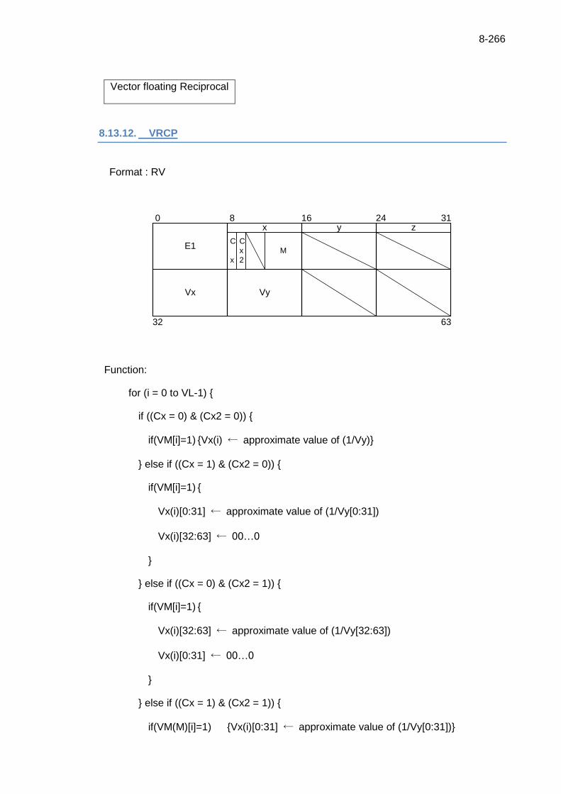
8-266
Vector floating Reciprocal
8.13.12. VRCP
Format : RV
x
E1
y z8 16 24 31
32 63
0
C
x
Vx Vy
M
C
x
2
Function:
for (i = 0 to VL-1) {
if ((Cx = 0) & (Cx2 = 0)) {
if(VM[i]=1) {Vx(i) ← approximate value of (1/Vy)}
} else if ((Cx = 1) & (Cx2 = 0)) {
if(VM[i]=1) {
Vx(i)[0:31] ← approximate value of (1/Vy[0:31])
Vx(i)[32:63] ← 00…0
}
} else if ((Cx = 0) & (Cx2 = 1)) {
if(VM[i]=1) {
Vx(i)[32:63] ← approximate value of (1/Vy[32:63])
Vx(i)[0:31] ← 00…0
}
} else if ((Cx = 1) & (Cx2 = 1)) {
if(VM(M)[i]=1) {Vx(i)[0:31] ← approximate value of (1/Vy[0:31])}
8-267
if((M=0) | (VM(M+1)[i] =1)) {Vx(i)[32:63] ← approximate value of
(1/Vy[32:63])}
}
}
The approximate value for the reciprocal of the contents of V register designated by Vy
is calculated. The results are stored into the V register designated by the Vx field.
When Cx=0 and Cx2=0, it operates as a double precision floating-point operation.
When Cx=0 and Cx2=1, it operates as a 32 bit single precision floating point operation
and its result is stored in the lower 32bits of the destination. The upper 32bits of the result
are filled with zeros.
When Cx=1 and Cx2=0, it operates as a 32 bit single precision floating point operation
and its result is stored in the upper 32bits of the destination.The lower 32bits of the result
are filled with zeros.
When Cx=1 and Cx2=1, it operates as a packed single precision floating-point
operation. Two VMs are employed in this case. M must be an even number. Otherwise,
an illegal instruction format exception is generated.
The precision of the approximation is system dependent.
This instruction is an element-maskable vector instruction.
Exceptions:
・Illegal instruction format exception
・Divide exception
・Floating-point underflow exception
・Invalid operation exception
・Inexact exception
・Illegal data format exception : When VL > MVL
Notes:
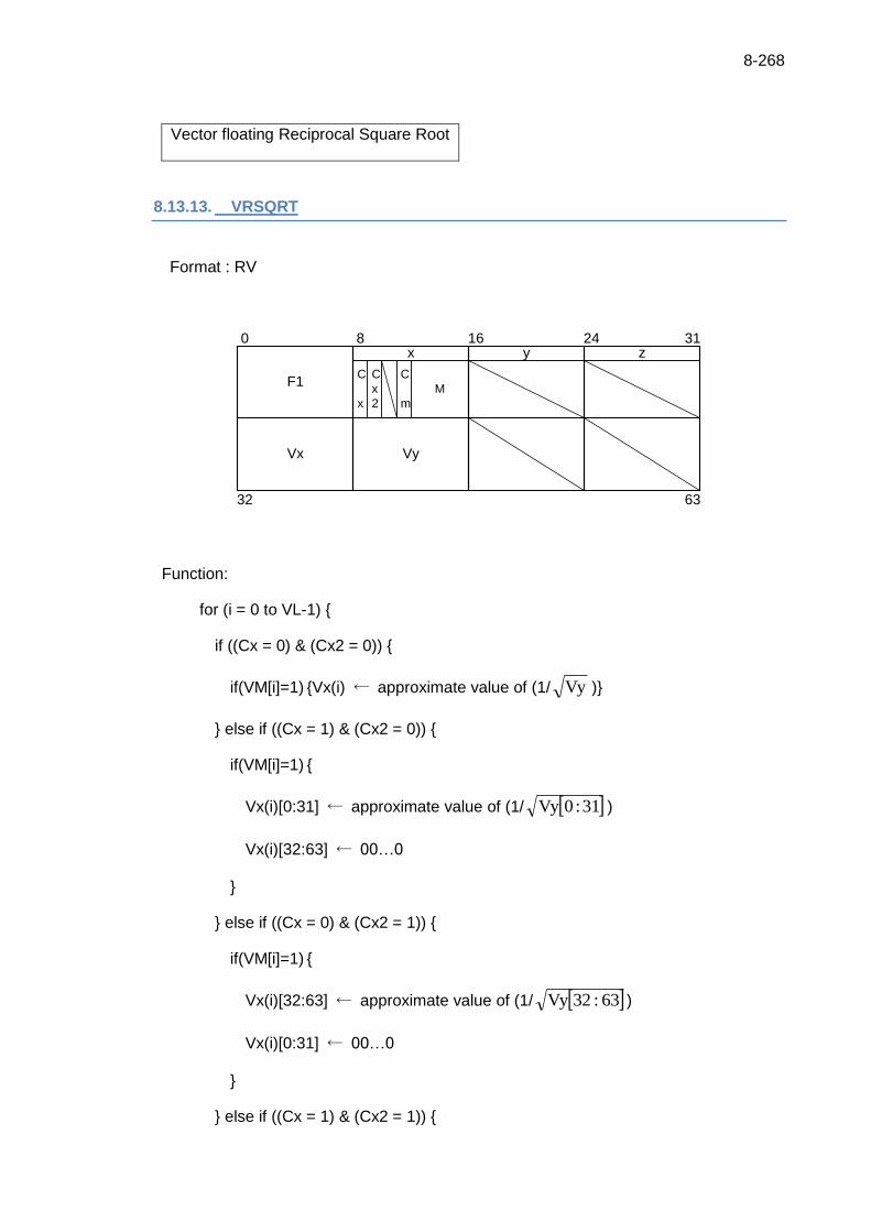
8-268
Vector floating Reciprocal Square Root
8.13.13. VRSQRT
Format : RV
x
F1
y z8 16 24 31
32 63
0
C
x
Vx Vy
M
C
m
C
x
2
Function:
for (i = 0 to VL-1) {
if ((Cx = 0) & (Cx2 = 0)) {
if(VM[i]=1) {Vx(i) ← approximate value of (1/ Vy )}
} else if ((Cx = 1) & (Cx2 = 0)) {
if(VM[i]=1) {
Vx(i)[0:31] ← approximate value of (1/ 31:0Vy )
Vx(i)[32:63] ← 00…0
}
} else if ((Cx = 0) & (Cx2 = 1)) {
if(VM[i]=1) {
Vx(i)[32:63] ← approximate value of (1/ 63:32Vy )
Vx(i)[0:31] ← 00…0
}
} else if ((Cx = 1) & (Cx2 = 1)) {
8-269
if(VM(M)[i]=1) {Vx(i)[0:31] ← approximate value of (1/ 31:0Vy )}
if((M=0) | (VM(M+1)[i] =1)) {Vx(i)[32:63] ← approximate value of (1/
63:32Vy )}
}
}
The approximate value for the reciprocal square root of the contents of V register
designated by Vy is calculated. The results are stored into the V register designated by
the Vx field.
The Cm field specifies the behavior of this operation at zero division. When Cm=0, a
division exception occurs and the result is infinity which has same sign with the input
value. When Cm=1, divide exception does not occur and the result is positive zero.
When Cx=0 and Cx2=0, it operates as a double precision floating-point operation.
When Cx=0 and Cx2=1, it operates as a 32 bit single precision floating point operation
and its result is stored in the lower 32bits of the destination. The upper 32bits of the result
are filled with zeros.
When Cx=1 and Cx2=0, it operates as a 32 bit single precision floating point operation
and its result is stored in the upper 32bits of the destination.The lower 32bits of the result
are filled with zeros.
When Cx=1 and Cx2=1, it operates as a packed single precision floating-point
operation. Two VMs are employed in this case. M must be an even number. Otherwise,
an illegal instruction format exception is generated.
The precision of the approximation is system dependent.
This instruction is an element-maskable vector instruction.
Exceptions:
・Illegal instruction format exception
・Divide exception
・Invalid operation exception
・Inexact exception
・Illegal data format exception : When VL > MVL
8-270
Vector Convert to Fixed Point
8.13.14. VFIX
Format : RV
x
E8
y z8 16 24 31
32 63
0
Vx Vy
M
C
x
C
m
Rvz
C
x
2
Function:
if ((Cm = 1) & (Cx = 0) & (Cx2 = 0)) {illegal instruction format exception}
for (i = 0 to VL-1) {
if (Cm = 0) {
if(VM[i]=1) {
if (Cx = 0) {Vx(i)[32:63] ← Convert double to int32(Vy)}
else {Vx(i)[32:63] ← Convert single to int32(Vy[0:31])}
if (Cx2 = 0) {Vx(i)[0:31] ← sext(Vx[32], 32)}
else {Vx(i)[0:31] ← 00…0}
}
} else /* if (Cm = 1) */ {
if ((Cx = 1) & (Cx2 = 0)) {
if(VM[i]=1) {
Vx(i)[0:31] ← Convert single to int32(Vy[0:31])
Vx(i)[32:63] ← 00…0
}
8-271
} else if ((Cx = 0) & (Cx2 = 1)) {
if(VM[i]=1) {
Vx(i)[32:63] ← Convert single to int32(Vy[32:63])
Vx(i)[0:31] ← 00…0
}
} else if ((Cx = 1) & (Cx2 = 1)) {
if(VM(M)[i]=1) {Vx(i)[0:31] ← Convert single to int32(Vy[0:31])}
if((M=0) | (VM(M+1)[i] =1)) {Vx(i)[32:63] ← Convert single to
int32(Vy[32:63])}
}
}
The contents of the V register designated by Vy field are converted from floating-point
data format to fixed-point data format. The results are stored into the V register
designated by Vx field.
The result is rounded to an integer according to the rounding mode specified by the
lowest 4bit of Rvz field as follows. When Rvz is not specified as a valid mode, the
conversion result is undefined.
0000:Round according to the IRM field in PSW.
1000:Round towards Zero
1001:Round towards Plus infinity
1010:Round towards Minus infinity
1011:Round to Nearest (ties to even)
1100:Round to Nearest (ties to away)
other:RFU
When Cm=0 and Cx=0, it operates as a conversion from double precision
floating-point data to 32-bit signed integer. The upper 32-bits of the result are filled with
extended sign if Cx2=0, or else filled with zero.
When Cm=0 and Cx=1, it operates as conversion from single precision floating-point
data to 32-bit signed integer. The upper 32-bits of the result are filled with extended sign
if Cx2=0, or else filled with zero.*
8-272
When Cm=1 and Cx=1 and Cx2=0, it operates like conversion from packed single
precision floating-point data to packed 32-bit signed integer, but the lower 32-bits of the
result are filled with zeros. Having M of an odd number is allowed.
When Cm=1 and Cx=0 and Cx2=1, it operates like conversion from packed single
precision floating-point data to packed 32-bit signed integer, but the upper 32 bits of the
result are filled with zeros. Having M of an odd number is allowed.
When Cm=1 and Cx=1 and Cx2=1, it operates as conversion from packed single
precision floating-point data to packed 32-bit signed integer. Two VMs are employed in
this case. M must be an even number. Otherwise, an illegal instruction format exception
is generated.
When Cm=1 and Cx=0 and Cs2=0, illegal instruction format exception occurs.
When the conversion result exceeds the representable range of 32-bit signed integer,
an invalid operation exception occurs. When an invalid operation exception occurs, the
result is undefined.
This instruction is an element-maskable vector instruction.
Exceptions:
・Illegal instruction format exception
・Invalid operation exception
・Inexact exception
・Illegal data format exception : When VL > MVL
Notes:
・Refer to a form change item in Chapter 4 about the numerical value expression
range of the change (restriction).
8-273
Vector Convert to Fixed Point
8.13.15. VFIXX
Format : RV
x
A8
y z8 16 24 31
32 63
0
Vx Vy
M
Rvz
Function:
for (i = 0 to VL-1) {
if(VM[i]=1) {Vx(i) ← Convert double to int64(Vy(i))}
}
The contents of the V register designated by Vy field are converted from floating-point
data format to fixed-point data format. The results are stored into the V register
designated by Vx field.
The result is rounded to an integer according to the rounding mode which is specified
by the lowest 4bit of Rvz field as follows. When Rvz =RFU, the conversion result is
undefined.
0000:Round according to the IRM field in PSW.
1000:Round toward Zero
1001:Round toward Plus infinity
1010:Round toward Minus infinity
1011:Round to Nearest (ties to even)
1100:Round to Nearest (ties to away)
8-274
other:RFU
It operates as a conversion from double precision floating-point data to 64-bit signed
integer.
When the conversion result exceeds the representable range of 64-bit signed integer,
an invalid operation exception occurs. When an invalid operation exception occurs, the
result is undefined.
This instruction is an element-maskable vector instruction.
Exceptions:
・Invalid operation exception
・Inexact exception
・Illegal data format exception : When VL > MVL
Notes:
・Refer to a form change item in Chapter 4 about the numerical value expression
range of the change (restriction).
8-275
Vector Convert to Floating Point
8.13.16. VFLT
Format : RV
x
F8
y z8 16 24 31
32 63
0
Vx Vy
M
C
x
C
m
C
x
2
Function:
if ((Cm = 1) & (Cx = 0) & (Cx2 = 0)) {illegal instruction format exception}
for (i = 0 to VL-1) {
if (Cm = 0) {
if(VM[i]=1) {
if (Cx = 0) {
Vx(i) ← Convert int32 to double(Vy)}
} else {
Vx(i)[0:31] ← Convert int32 to single(Vy[32:63])
Vx(i)[32:63] ← 00…0
}
}
} else {
if ((Cx = 1) & (Cx2 = 0)) {
if(VM[i]=1) {
Vx(i)[0:31] ← Convert int32 to single(Vy[0:31])
8-276
Vx(i)[32:63] ← 00…0
}
} else if ((Cx = 0) & (Cx2 = 1)) {
if(VM[i]=1) {
Vx(i)[32:63] ← Convert int32 to single(Vy[32:63])
Vx(i)[0:31] ← 00…0
}
} else if ((Cx = 1) & (Cx2 = 1)) {
if(VM(M)[i]=1) {Vx(i)[0:31] ← Convert int32 to single(Vy[0:31])}
if((M=0) | (VM(M+1)[i] =1)) {Vx(i)[32:63] ← Convert int32 to
single(Vy[32:63])}
}
}
The contents of the V register designated by Vy field are converted from fixed-point
data format to floating-point data format. The results are stored into the V register
designated by Vx field.
When Cm=0 and Cx=0, it operates as a conversion from 32-bit signed integer to
double precision floating-point data.
When Cm=0 and Cx=1, it operates as a conversion from 32-bit signed integer to single
precision floating-point data. The lower 32-bits of the result are filled with zero.
When Cm=1 and Cx=1 and Cx2=0, it operates as a conversion from packed 32-bit
signed integer to packed single precision floating-point data, but the lower 32-bits of the
result are filled with zeros. Having M of an odd number is allowed.
When Cm=1 and Cx=0 and Cx2=1, it operates like a conversion from packed 32-bit
signed integer to packed single precision floating-point data, but the upper 32 bits of the
result are filled with zeros. Having M of an odd number is allowed.
When Cm=1 and Cx=1 and Cx2=1, it operates like a conversion from packed 32-bit
signed integer to packed single precision floating-point data. Two VMs are employed in
this case. M must be an even number. Otherwise, an illegal instruction format exception
is generated.
When Cm=1 and Cx=0 and Cs2=0, illegal instruction format exception occurs.
8-277
An inexact exception is raised when the conversion results in degradation of the
precision.
This instruction is an element-maskable vector instruction.
Exceptions:
・Illegal instruction format exception
・Inexact exception
・Illegal data format exception : When VL > MVL
Notes:
8-278
Vector Convert to Floating Point
8.13.17. VFLTX
Format : RV
x
B8
y z8 16 24 31
32 63
0
Vx Vy
M
Function:
for (i = 0 to VL-1) {
if(VM[i]=1) {Vx(i) ← Convert int64 to double(Vy(i))}
}
The contents of the V register designated by Vy field are converted from fixed-point
data format to floating-point data format. The results are stored into the V register
designated by Vx field.
It operates as a conversion from 64-bit signed integer to double precision floating-point
data.
An inexact exception is raised when the conversion results in degradation of the
precision.
This instruction is an element-maskable vector instruction.
Exceptions:
・Inexact exception
・Illegal data format exception : When VL > MVL
8-279
Vector Convert to Single-format
8.13.18. VCVS
Format : RV
x
9F
y z8 16 24 31
32 63
0
Vx Vy
M
Function:
for (i = 0 to VL-1) {
if(VM[i]=1) {
Vx(i)[0:31]← Convert double to single(Vy(i))
Vx(i)[32:63]← 00…0
}
}
The contents of the V register designated by Vy field are converted from double
precision floating-point data format to single precision floating-point data format. The
results are stored into the V register designated by Vx field.
This instruction is an element-maskable vector instruction.
Exceptions:
・floating-point overflow exception
・floating-point underflow exception
・Invalid operation exception
・Inexact exception
・Illegal data format exception : When VL > MVL
8-280
Vector Convert to Double-format
8.13.19. VCVD
Format : RV
x
8F
y z8 16 24 31
32 63
0
Vx Vy
M
Function:
for (i = 0 to VL-1) {
if(VM[i]=1) {Vx(i) ← Convert single to double(Vy(i)[0:31])}
}
The contents of the V register designated by Vy field are converted from single
precision floating-point data format to double precision floating-point data format. The
results are stored into the V register designated by Vx field.
This instruction is an element-maskable vector instruction.
Exceptions:
・Invalid operation exception
・Illegal data format exception : When VL > MVL
Notes:
8-281
8.14. Vector Reduction Instructions
Vector Sum Single
8.14.1. VSUMS
Format : RV
x
EA
y z8 16 24 31
32 63
0
Vx Vy
M
C
x
2
Function:
for (i = 0 to VL-1) {
if(VM[i]=1) {tempY(i) ← Vy(i)}
else {tempY(i) ← 0}
}
Vx(0)[32:63] ← Σ(tempY(0)[32:63], tempY(1)[32:63], ……, tempY(VL-1)[32:63])
if (Cx2 = 0) {Vx(0)[0:31] ← sext(Vx(0)[32], 32)}
else {Vx(0)[0:31] ← 00…0}
The 32-bit signed interger sum of elements 0 to VL of the V register designated by Vy
field is calculated, and the result is stored in the lower 32 bits of element 0 of the V
register designated by Vx field.
When Cx2=0, the bits 0 to 31 of V register designated by Vx field are filled with the
value of bit 32 for sign extension. When Cx2=1, the bits 0 to 31 of V register designated
by Vx field are filled with zero.
8-282
The calculation order of the summation is system dependent.
This instruction is an element-maskable vector instruction. The elements with mask=1
are only taken for calculation. The elements with mask=0 are ignored.
When the masks for elements 0 to VL-1 are all 0, the result is 0.
When Fixed-point overflow exception occurs by the calculation, the result is undefined.
Exceptions:
・Fixed-point overflow exception
・Illegal data format exception : When VL > MVL
Notes:
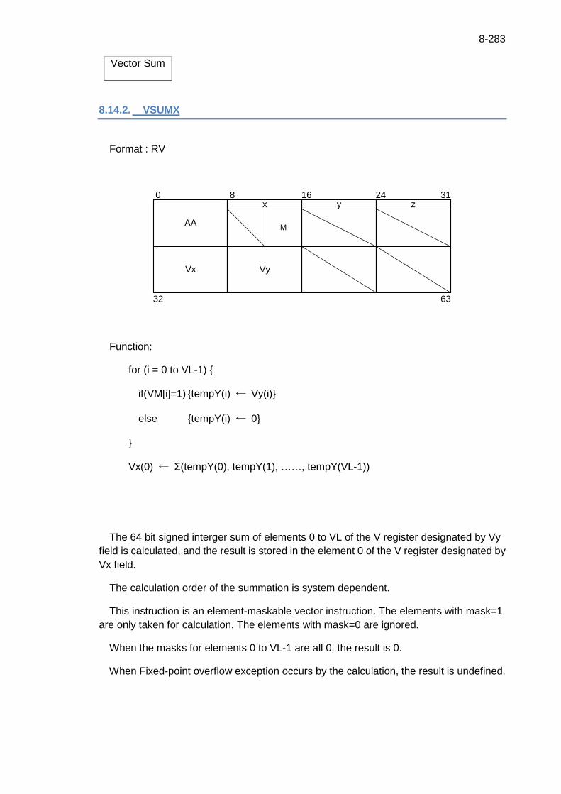
8-283
Vector Sum
8.14.2. VSUMX
Format : RV
x
AA
y z8 16 24 31
32 63
0
Vx Vy
M
Function:
for (i = 0 to VL-1) {
if(VM[i]=1) {tempY(i) ← Vy(i)}
else {tempY(i) ← 0}
}
Vx(0) ← Σ(tempY(0), tempY(1), ……, tempY(VL-1))
The 64 bit signed interger sum of elements 0 to VL of the V register designated by Vy
field is calculated, and the result is stored in the element 0 of the V register designated by
Vx field.
The calculation order of the summation is system dependent.
This instruction is an element-maskable vector instruction. The elements with mask=1
are only taken for calculation. The elements with mask=0 are ignored.
When the masks for elements 0 to VL-1 are all 0, the result is 0.
When Fixed-point overflow exception occurs by the calculation, the result is undefined.

8-284
Exceptions:
・Fixed-point overflow exception
・Illegal data format exception : When VL > MVL
Notes:
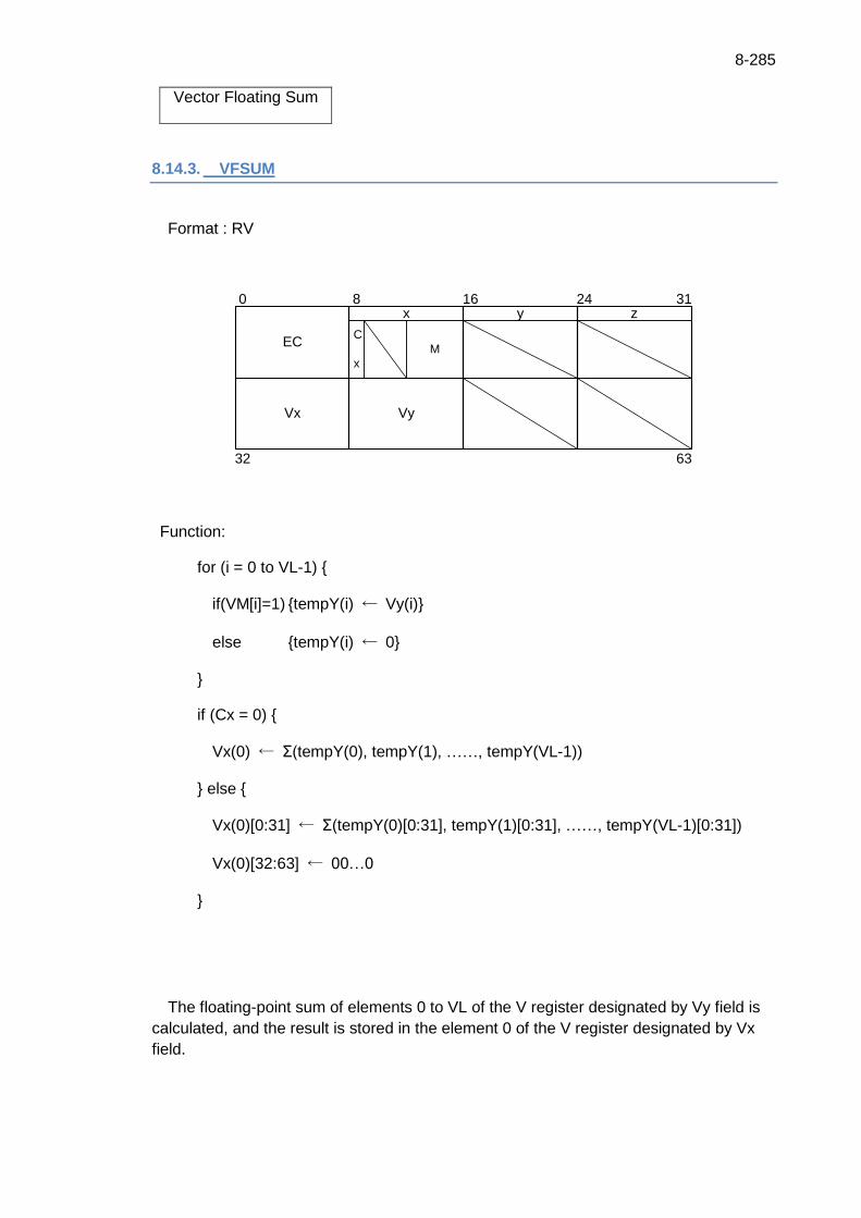
8-285
Vector Floating Sum
8.14.3. VFSUM
Format : RV
x
EC
y z8 16 24 31
32 63
0
C
x
Vx Vy
M
Function:
for (i = 0 to VL-1) {
if(VM[i]=1) {tempY(i) ← Vy(i)}
else {tempY(i) ← 0}
}
if (Cx = 0) {
Vx(0) ← Σ(tempY(0), tempY(1), ……, tempY(VL-1))
} else {
Vx(0)[0:31] ← Σ(tempY(0)[0:31], tempY(1)[0:31], ……, tempY(VL-1)[0:31])
Vx(0)[32:63] ← 00…0
}
The floating-point sum of elements 0 to VL of the V register designated by Vy field is
calculated, and the result is stored in the element 0 of the V register designated by Vx
field.
8-286
When Cx=0, the input data and the result are regarded as double-precision floating
point data. When Cx=1, it is regarded as single-precision floating point data.
The calculation order of the summation and normalization is system dependent.
When Floating-point overflow exception or Floating-point underflow exception occurs
by the calculation, the result is undefined.
When the input data is NaN, invalid operation exception occurs and the result is NaN.
This instruction is an element-maskable vector instruction. The elements with mask=1
are only taken for calculation. The elements with mask=0 are ignored.
When the masks for elements 0 to VL-1 are all 0, the result is 0.
Exceptions:
・Floating-point overflow exception
・Floating-point underflow exception
・Invalid operation exception
・Inexact exception
・Illegal data format exception : When VL > MVL
Notes:
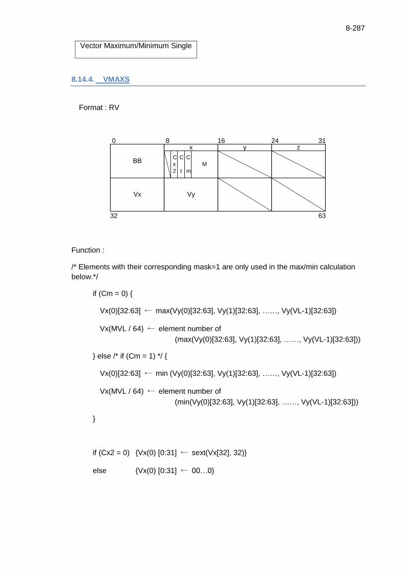
8-287
Vector Maximum/Minimum Single
8.14.4. VMAXS
Format : RV
x
BB
y z8 16 24 31
32 63
0
Vx Vy
M
C
t
C
m
C
x
2
Function :
/* Elements with their corresponding mask=1 are only used in the max/min calculation
below.*/
if (Cm = 0) {
Vx(0)[32:63] ← max(Vy(0)[32:63], Vy(1)[32:63], ……, Vy(VL-1)[32:63])
Vx(MVL / 64) ← element number of
(max(Vy(0)[32:63], Vy(1)[32:63], ……, Vy(VL-1)[32:63]))
} else /* if (Cm = 1) */ {
Vx(0)[32:63] ← min (Vy(0)[32:63], Vy(1)[32:63], ……, Vy(VL-1)[32:63])
Vx(MVL / 64) ← element number of
(min(Vy(0)[32:63], Vy(1)[32:63], ……, Vy(VL-1)[32:63]))
}
if (Cx2 = 0) {Vx(0) [0:31] ← sext(Vx[32], 32)}
else {Vx(0) [0:31] ← 00…0}
8-288
An element with the largest/smallest value as a 32 bit signed integer is searched from
the elements 0 to VL-1 of the V register specified by Vy field. The upper 32 bits of the Vy
register elements are not referred in this operation. When Cm=0, largest element is
chosen, otherwise the smallest one is taken as the result. The max/min result is stored in
element 0 of the V register specified by the x field.
When Cx2=0, the upper 32-bits of the result are filled with extended sign bits. When
Cx2=1, the upper 32-bits of the result are filled with zeros.
The element position corresponding to the maximum value (Cm=0) or the minimum
value (Cm=1) is also stored in the element MVL/64 of the V register specified by the x
field at the same time.
When multiple elements contain the maximum (Cm=0) or minimum value (Cm=1), the
result element position is specified by the Ct bit as follows. If Ct=0, the result is the
element position at which the result value is firstly found (the smallest position number.) If
Ct=1, the result is the last element position at which the result value is found (the largest
position number.)
This instruction is an element-maskable vector instruction. Only elements with mask =
1 are taken for this computation. The elements with mask = 0 are ignored. When mask
bits for elements 0 to VL-1 are all 0, the result max/min value of this operation is 0 and
the element number returned for this operation is 64bits of 1 (111..111) .
Exceptions:
・Illegal data format exception : When VL > MVL
Notes:
・MVL is 256 in Aurora.
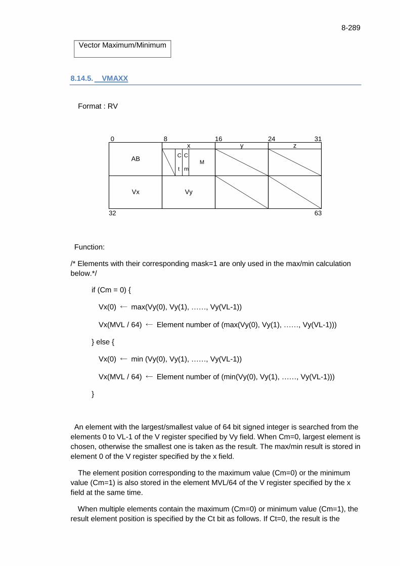
8-289
Vector Maximum/Minimum
8.14.5. VMAXX
Format : RV
x
AB
y z8 16 24 31
32 63
0
Vx Vy
M
C
t
C
m
Function:
/* Elements with their corresponding mask=1 are only used in the max/min calculation
below.*/
if (Cm = 0) {
Vx(0) ← max(Vy(0), Vy(1), ……, Vy(VL-1))
Vx(MVL / 64) ← Element number of (max(Vy(0), Vy(1), ……, Vy(VL-1)))
} else {
Vx(0) ← min (Vy(0), Vy(1), ……, Vy(VL-1))
Vx(MVL / 64) ← Element number of (min(Vy(0), Vy(1), ……, Vy(VL-1)))
}
An element with the largest/smallest value of 64 bit signed integer is searched from the
elements 0 to VL-1 of the V register specified by Vy field. When Cm=0, largest element is
chosen, otherwise the smallest one is taken as the result. The max/min result is stored in
element 0 of the V register specified by the x field.
The element position corresponding to the maximum value (Cm=0) or the minimum
value (Cm=1) is also stored in the element MVL/64 of the V register specified by the x
field at the same time.
When multiple elements contain the maximum (Cm=0) or minimum value (Cm=1), the
result element position is specified by the Ct bit as follows. If Ct=0, the result is the
8-290
element position at which the result value is firstly found (the smallest position number.) If
Ct=1, the result is the last element position at which the result value is found (the largest
position number.)
This instruction is an element-maskable vector instruction. Only elements with mask =
1 are taken for this computation. The elements with mask = 0 are ignored. When mask
bits for elements 0 to VL-1 are all 0, the result max/min value of this operation is 0 and
the element number returned for this operation is 64bits of 1 (111..111) .
Exceptions:
・Illegal data format exception : When VL > MVL
Notes:
・MVL is 256 in Aurora.
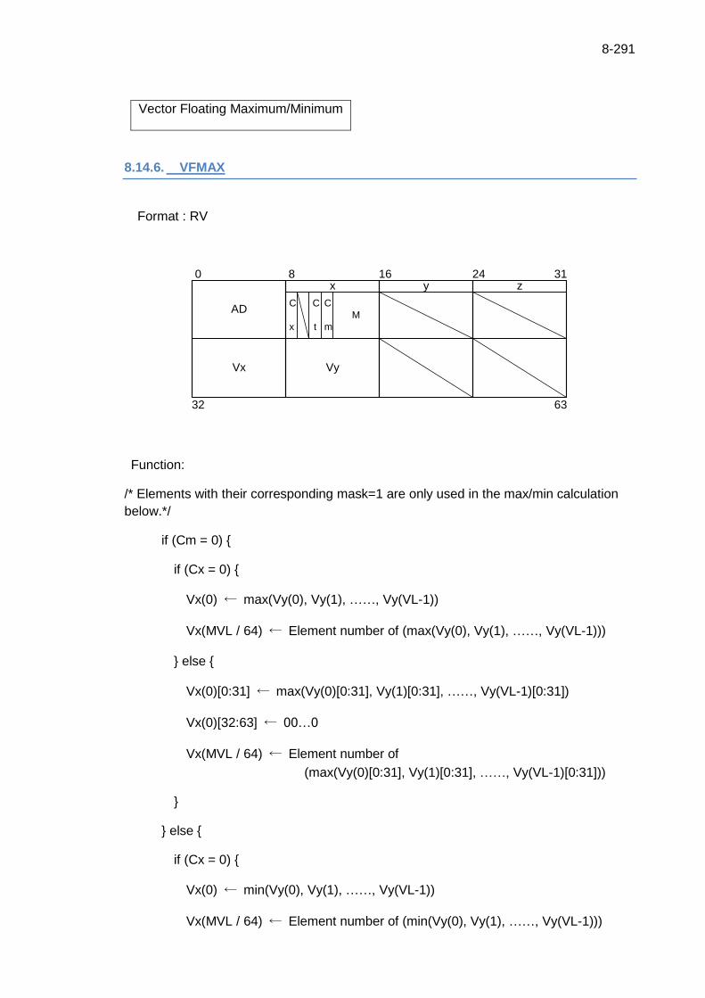
8-291
Vector Floating Maximum/Minimum
8.14.6. VFMAX
Format : RV
x
AD
y z8 16 24 31
32 63
0
C
x
Vx Vy
M
C
t
C
m
Function:
/* Elements with their corresponding mask=1 are only used in the max/min calculation
below.*/
if (Cm = 0) {
if (Cx = 0) {
Vx(0) ← max(Vy(0), Vy(1), ……, Vy(VL-1))
Vx(MVL / 64) ← Element number of (max(Vy(0), Vy(1), ……, Vy(VL-1)))
} else {
Vx(0)[0:31] ← max(Vy(0)[0:31], Vy(1)[0:31], ……, Vy(VL-1)[0:31])
Vx(0)[32:63] ← 00…0
Vx(MVL / 64) ← Element number of
(max(Vy(0)[0:31], Vy(1)[0:31], ……, Vy(VL-1)[0:31]))
}
} else {
if (Cx = 0) {
Vx(0) ← min(Vy(0), Vy(1), ……, Vy(VL-1))
Vx(MVL / 64) ← Element number of (min(Vy(0), Vy(1), ……, Vy(VL-1)))
8-292
} else {
Vx(0)[0:31] ← min(Vy(0)[0:31], Vy(1)[0:31], ……, Vy(VL-1)[0:31])
Vx(0)[32:63] ← 00…0
Vx(MVL / 64) ← Element number of
(min(Vy(0)[0:31], Vy(1)[0:31], ……, Vy(VL-1)[0:31]))
}
}
An element with the largest/smallest floating point value is searched from the elements
0 to VL-1 of the V register specified by Vy field. When Cm=0, largest element is chosen,
otherwise the smallest one is taken as the result. The max/min result is stored in element
0 of the V register specified by the x field.
The element position corresponding to the maximum value (Cm=0) or the minimum
value (Cm=1) is also stored in the element MVL/64 of the V register specified by the x
field at the same time.
When multiple elements contain the maximum (Cm=0) or minimum value (Cm=1), the
result element position is specified by the Ct bit as follows. If Ct=0, the result is the
element position at which the result value is firstly found (the smallest position number.) If
Ct=1, the result is the last element position at which the result value is found (the largest
position number.)
This instruction is an element-maskable vector instruction. Only elements with mask =
1 are taken for this computation. The elements with mask = 0 are ignored. When mask
bits for elements 0 to VL-1 are all 0, the result max/min value of this operation is 0 and
the element number returned for this operation is 64bits of 1 (111..111) .
When Cx=0, the input data and the result are regarded as double-precision floating
point data. When Cx=1, it is regarded as single-precision floating point data.
When any of the input data is sNaN, invalid operation exception occurs and the results
are undefined.
When all of the input data is qNaN, the result for maximum/minimum value is qNaN and
the element number is any of element number which mask is ‘1’.
+0 and -0 are regarded as the same value. If the maximum/minimum value is zero and
there are multiple elements equal to zero, the result for maximum/minimum value is zero
with the sign of the element which is specified by the Ct bit in the same manner with
element number result.
Exceptions:

8-293
・Invalid operation exception
・Illegal data format exception : When VL > MVL
Notes:
・MVL is 256 in Aurora.
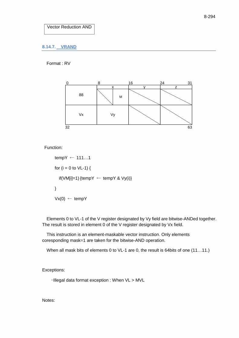
8-294
Vector Reduction AND
8.14.7. VRAND
Format : RV
x
88
y z8 16 24 31
32 63
0
Vx Vy
M
Function:
tempY ← 111…1
for (i = 0 to VL-1) {
if(VM[i]=1) {tempY ← tempY & Vy(i)}
}
Vx(0) ← tempY
Elements 0 to VL-1 of the V register designated by Vy field are bitwise-ANDed together.
The result is stored in element 0 of the V register designated by Vx field.
This instruction is an element-maskable vector instruction. Only elements
coresponding mask=1 are taken for the bitwise-AND operation.
When all mask bits of elements 0 to VL-1 are 0, the result is 64bits of one (11…11.)
Exceptions:
・Illegal data format exception : When VL > MVL
Notes:
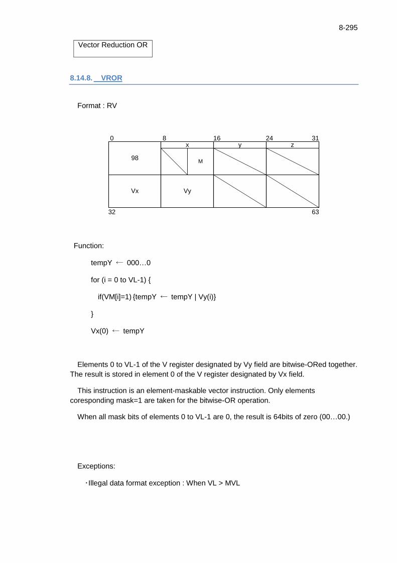
8-295
Vector Reduction OR
8.14.8. VROR
Format : RV
x
98
y z8 16 24 31
32 63
0
Vx Vy
M
Function:
tempY ← 000…0
for (i = 0 to VL-1) {
if(VM[i]=1) {tempY ← tempY | Vy(i)}
}
Vx(0) ← tempY
Elements 0 to VL-1 of the V register designated by Vy field are bitwise-ORed together.
The result is stored in element 0 of the V register designated by Vx field.
This instruction is an element-maskable vector instruction. Only elements
coresponding mask=1 are taken for the bitwise-OR operation.
When all mask bits of elements 0 to VL-1 are 0, the result is 64bits of zero (00…00.)
Exceptions:
・Illegal data format exception : When VL > MVL
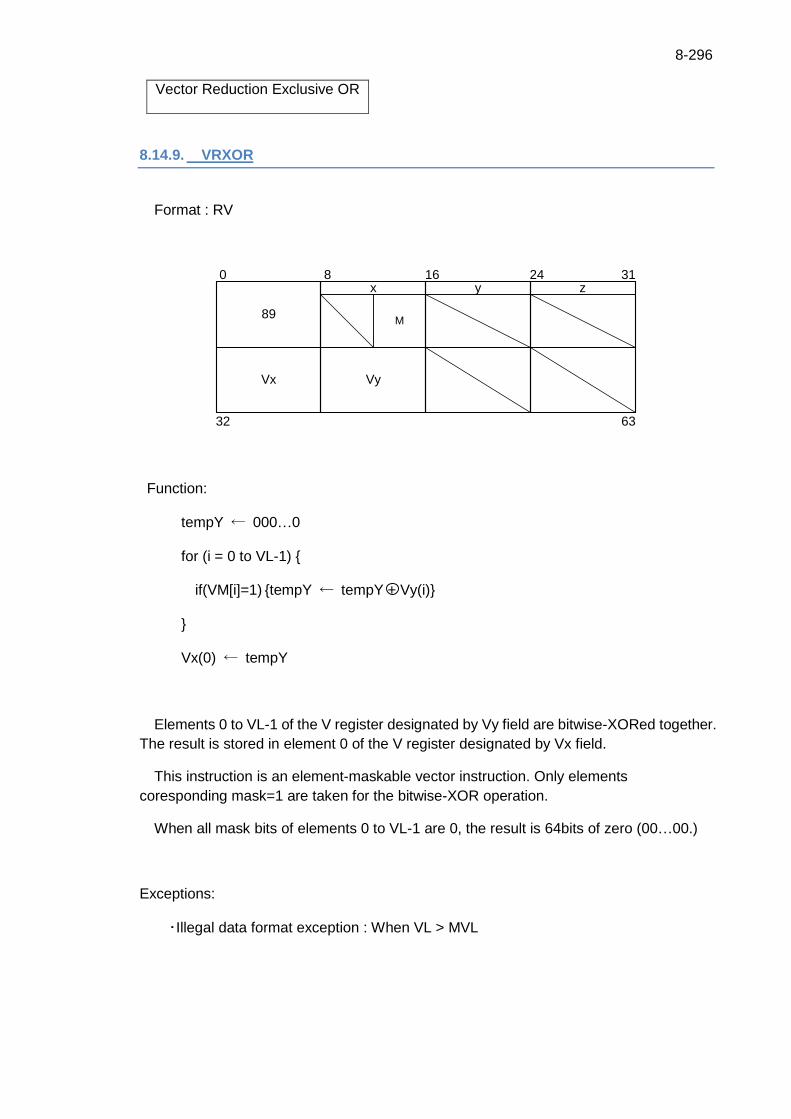
8-296
Vector Reduction Exclusive OR
8.14.9. VRXOR
Format : RV
x
89
y z8 16 24 31
32 63
0
Vx Vy
M
Function:
tempY ← 000…0
for (i = 0 to VL-1) {
if(VM[i]=1) {tempY ← tempY + Vy(i)}
}
Vx(0) ← tempY
Elements 0 to VL-1 of the V register designated by Vy field are bitwise-XORed together.
The result is stored in element 0 of the V register designated by Vx field.
This instruction is an element-maskable vector instruction. Only elements
coresponding mask=1 are taken for the bitwise-XOR operation.
When all mask bits of elements 0 to VL-1 are 0, the result is 64bits of zero (00…00.)
Exceptions:
・Illegal data format exception : When VL > MVL
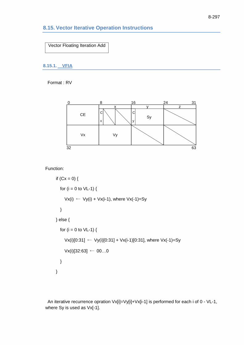
8-297
8.15. Vector Iterative Operation Instructions
Vector Floating Iteration Add
8.15.1. VFIA
Format : RV
x
CE
y z8 16 24 31
32 63
0
Vx Vy
SyC
x
C
y
Function:
if (Cx = 0) {
for (i = 0 to VL-1) {
Vx(i) ← Vy(i) + Vx(i-1), where Vx(-1)=Sy
}
} else {
for (i = 0 to VL-1) {
Vx(i)[0:31] ← Vy(i)[0:31] + Vx(i-1)[0:31], where Vx(-1)=Sy
Vx(i)[32:63] ← 00…0
}
}
An iterative recurrence opration Vx[i]=Vy[i]+Vx[i-1] is performed for each i of 0 - VL-1,
where Sy is used as Vx[-1].
8-298
Vx indicates the V register designated by Vx field, and Vy is the V register designated
by Vy field. Vx[i] is the i-th element of Vx, Vy[i] is Vy’s element i.
When Cx=0, the input data and the result are regarded as double-precision floating
point data, otherwise (when Cx=1) it is regarded as single-precision floating point data.
This instruction doesn’t have the element masking feature.
Exceptions:
・Floating-point overflow exception
・Floating-point underflow exception
・Invalid operation exception
・Inexact exception
・Illegal data format exception : When VL > MVL
Notes:
・When Cy=0, y operand is the immediate value of signed integers( -64 ~ 63).
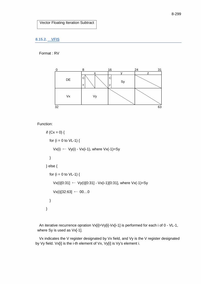
8-299
Vector Floating Iteration Subtract
8.15.2. VFIS
Format : RV
x
DE
y z8 16 24 31
32 63
0
Vx Vy
SyC
x
C
y
Function:
if (Cx = 0) {
for (i = 0 to VL-1) {
Vx(i) ← Vy(i) - Vx(i-1), where Vx(-1)=Sy
}
} else {
for (i = 0 to VL-1) {
Vx(i)[0:31] ← Vy(i)[0:31] - Vx(i-1)[0:31], where Vx(-1)=Sy
Vx(i)[32:63] ← 00…0
}
}
An iterative recurrence opration Vx[i]=Vy[i]-Vx[i-1] is performed for each i of 0 - VL-1,
where Sy is used as Vx[-1].
Vx indicates the V register designated by Vx field, and Vy is the V register designated
by Vy field. Vx[i] is the i-th element of Vx, Vy[i] is Vy’s element i.

8-300
When Cx=0, the input data and the result are regarded as double-precision floating
point data, otherwise (when Cx=1) it is regarded as single-precision floating point data.
This instruction doesn’t have the element masking feature.
Exceptions:
・Floating-point overflow exception
・Floating-point underflow exception
・Invalid operation exception
・Inexact exception
・Illegal data format exception : When VL > MVL
Notes:
・When Cy=0, y operand is the immediate value of signed integers( -64 ~ 63).
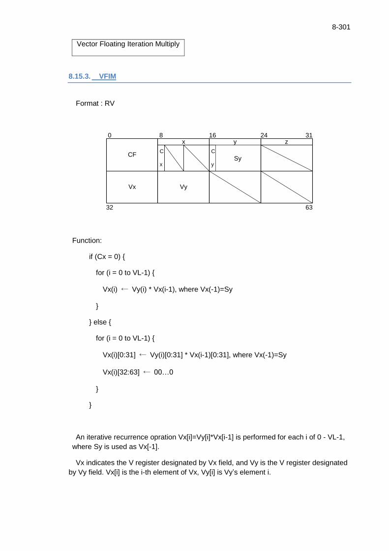
8-301
Vector Floating Iteration Multiply
8.15.3. VFIM
Format : RV
x
CF
y z8 16 24 31
32 63
0
Vx Vy
C
x Sy
C
y
Function:
if (Cx = 0) {
for (i = 0 to VL-1) {
Vx(i) ← Vy(i) * Vx(i-1), where Vx(-1)=Sy
}
} else {
for (i = 0 to VL-1) {
Vx(i)[0:31] ← Vy(i)[0:31] * Vx(i-1)[0:31], where Vx(-1)=Sy
Vx(i)[32:63] ← 00…0
}
}
An iterative recurrence opration Vx[i]=Vy[i]*Vx[i-1] is performed for each i of 0 - VL-1,
where Sy is used as Vx[-1].
Vx indicates the V register designated by Vx field, and Vy is the V register designated
by Vy field. Vx[i] is the i-th element of Vx, Vy[i] is Vy’s element i.

8-302
When Cx=0, the input data and the result are regarded as double-precision floating
point data, otherwise (when Cx=1) it is regarded as single-precision floating point data.
This instruction doesn’t have the element masking feature.
Exceptions:
・Floating-point overflow exception
・Floating-point underflow exception
・Invalid operation exception
・Inexact exception
・Illegal data format exception : When VL > MVL
Notes:
・When Cy=0, y operand is the immediate value of signed integers( -64 ~ 63).
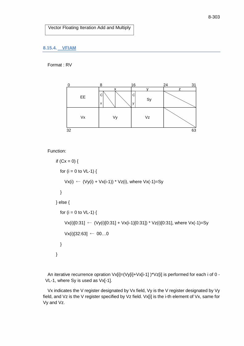
8-303
Vector Floating Iteration Add and Multiply
8.15.4. VFIAM
Format : RV
x
EE Sy
y
C
y
z8 16 24 31
32 63
0
Vx Vy Vz
C
x
Function:
if (Cx = 0) {
for (i = 0 to VL-1) {
Vx(i) ← (Vy(i) + Vx(i-1)) * Vz(i), where Vx(-1)=Sy
}
} else {
for (i = 0 to VL-1) {
Vx(i)[0:31] ← (Vy(i)[0:31] + Vx(i-1)[0:31]) * Vz(i)[0:31], where Vx(-1)=Sy
Vx(i)[32:63] ← 00…0
}
}
An iterative recurrence opration Vx[i]=(Vy[i]+Vx[i-1] )*Vz[i] is performed for each i of 0 -
VL-1, where Sy is used as Vx[-1].
Vx indicates the V register designated by Vx field, Vy is the V register designated by Vy
field, and Vz is the V register specified by Vz field. Vx[i] is the i-th element of Vx, same for
Vy and Vz.

8-304
When Cx=0, the input data and the result are regarded as double-precision floating
point data, otherwise (when Cx=1) it is regarded as single-precision floating point data.
This instruction doesn’t have the element masking feature.
Exceptions:
・Floating-point overflow exception
・Floating-point underflow exception
・Invalid operation exception
・Inexact exception
・Illegal data format exception : When VL > MVL
Notes:
・When Cy=0, y operand is the immediate value of signed integers( -64 ~ 63).
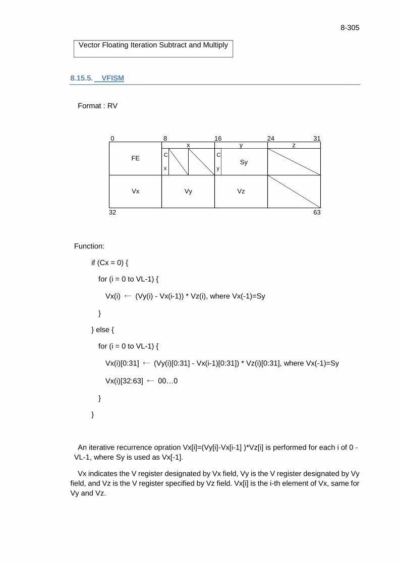
8-305
Vector Floating Iteration Subtract and Multiply
8.15.5. VFISM
Format : RV
x
FE Sy
y
C
y
z8 16 24 31
32 63
0
Vx Vy Vz
C
x
Function:
if (Cx = 0) {
for (i = 0 to VL-1) {
Vx(i) ← (Vy(i) - Vx(i-1)) * Vz(i), where Vx(-1)=Sy
}
} else {
for (i = 0 to VL-1) {
Vx(i)[0:31] ← (Vy(i)[0:31] - Vx(i-1)[0:31]) * Vz(i)[0:31], where Vx(-1)=Sy
Vx(i)[32:63] ← 00…0
}
}
An iterative recurrence opration Vx[i]=(Vy[i]-Vx[i-1] )*Vz[i] is performed for each i of 0 -
VL-1, where Sy is used as Vx[-1].
Vx indicates the V register designated by Vx field, Vy is the V register designated by Vy
field, and Vz is the V register specified by Vz field. Vx[i] is the i-th element of Vx, same for
Vy and Vz.

8-306
When Cx=0, the input data and the result are regarded as double-precision floating
point data, otherwise (when Cx=1) it is regarded as single-precision floating point data.
This instruction doesn’t have the element masking feature.
Exceptions:
・Floating-point overflow exception
・Floating-point underflow exception
・Invalid operation exception
・Inexact exception
・Illegal data format exception : When VL > MVL
Notes:
・When Cy=0, y operand is the immediate value of signed integers( -64 ~ 63).
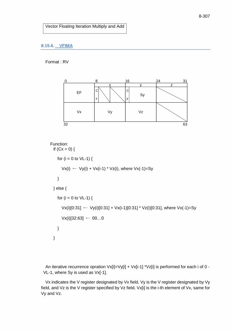
8-307
Vector Floating Iteration Multiply and Add
8.15.6. VFIMA
Format : RV
x
EF Sy
y
C
y
z8 16 24 31
32 63
0
Vx Vy Vz
C
x
Function: if (Cx = 0) {
for (i = 0 to VL-1) {
Vx(i) ← Vy(i) + Vx(i-1) * Vz(i), where Vx(-1)=Sy
}
} else {
for (i = 0 to VL-1) {
Vx(i)[0:31] ← Vy(i)[0:31] + Vx(i-1)[0:31] * Vz(i)[0:31], where Vx(-1)=Sy
Vx(i)[32:63] ← 00…0
}
}
An iterative recurrence opration Vx[i]=Vy[i] + Vx[i-1] *Vz[i] is performed for each i of 0 -
VL-1, where Sy is used as Vx[-1].
Vx indicates the V register designated by Vx field, Vy is the V register designated by Vy
field, and Vz is the V register specified by Vz field. Vx[i] is the i-th element of Vx, same for
Vy and Vz.
8-308
When Cx=0, the input data and the result are regarded as double-precision floating
point data, otherwise (when Cx=1) it is regarded as single-precision floating point data.
This instruction doesn’t have the element masking feature.
Exceptions:
・Floating-point overflow exception
・Floating-point underflow exception
・Invalid operation exception
・Inexact exception
・Illegal data format exception : When VL > MVL
Notes:
・When Cy=0, y operand is the immediate value of signed integers( -64 ~ 63).
8-309
Vector Floating Iteration Multiply and Subtract
8.15.7. VFIMS
Format : RV
x
FF
y z8 16 24 31
32 63
0
Vx Vy Vz
SyC
y
C
x
Function:
if (Cx = 0) {
for (i = 0 to VL-1) {
Vx(i) ← Vy(i) - Vx(i-1) * Vz(i), where Vx(-1)=Sy
}
} else {
for (i = 0 to VL-1) {
Vx(i)[0:31] ← Vy(i)[0:31] - Vx(i-1)[0:31] * Vz(i)[0:31], where Vx(-1)=Sy
Vx(i)[32:63] ← 00…0
}
}
An iterative recurrence opration Vx[i]=Vy[i] - Vx[i-1] *Vz[i] is performed for each i of 0 -
VL-1, where Sy is used as Vx[-1].
Vx indicates the V register designated by Vx field, Vy is the V register designated by Vy
field, and Vz is the V register specified by Vz field. Vx[i] is the i-th element of Vx, same for
Vy and Vz.

8-310
When Cx=0, the input data and the result are regarded as double-precision floating
point data, otherwise (when Cx=1) it is regarded as single-precision floating point data.
This instruction doesn’t have the element masking feature.
Exceptions:
・Floating-point overflow exception
・Floating-point underflow exception
・Invalid operation exception
・Inexact exception
・Illegal data format exception : When VL > MVL
Notes:
・When Cy=0, y operand is the immediate value of signed integers( -64 ~ 63).

8-311
8.16. Vector Merger Operation Instructions
Vector Merge
8.16.1. VMRG
Format : RV
x
D6 Sy
y
C
y
z8 16 24 31
32 63
0
Vx Vy Vz
M
C
s
C
x
Function: for (i = 0 to VL-1) {
if(Cx = 0) {
if(Cs = 0) {Vx(i) ← VM[i] ? Vz(i) : Vy(i)}
else {Vx(i) ← VM[i] ? Vz(i) : Sy}
} else {
if(Cs = 0) {
Vx(i)[0:31] ← VM(M)[i] ? Vz(i)[0:31] : Vy(i)[0:31]
Vx(i)[32:63] ← VM(M+1)[i] ? Vz(i)[32:63] : Vy(i)[32:63]
} else {
Vx(i)[0:31] ← VM(M)[i] ? Vz(i)[0:31] : Sy[0:31]
Vx(i)[32:63] ← VM(M+1)[i] ? Vz(i)[32:63] : Sy[32:63]
}
}
}
8-312
Note: When M=0, VM(0) is used instead of VM(M+1).
A ternary operation using a VM register as a condition is performed and the result is
stored to each of elements 0 to VL-1 of the V register specified by Vx field.
The VM register is specified by the M field. According to each mask bit in the VM, Vz, Vy
or Sy value is selected. When the VM’s mask bit is 1, Vz is selected. Otherwise Sy is
chosen if Cs=1, or Vz is selected if Cs=0.
This operation doesn’t support element masking feature.
When Cx=0, it operates as a 64-bit logical operation.
When Cx=1, it operates as an operation for packed 32-bit logical data. Two VMs are
employed, and M must be an even number then. Otherwise an illegal instruction format
exception is generated.
Exceptions:
・Illegal instruction format exception
・Illegal data format exception : When VL > MVL
Notes:
・When (Cs=1) and (Cy=0)), y operand is the immediate value of signed integers( -64 ~
63).
8-313
Vector Shuffle
8.16.2. VSHF
Format : RV
x
BC Sy
y
C
y
z8 16 24 31
32 63
0
Vx Vy Vz
Function:
for (i = 0 to VL-1) {
if (Sy[60:61] = 00) {Vx[0:31] ← Vy[0:31]}
else if (Sy[60:61] = 01) {Vx[0:31] ← Vy[32:63]}
else if (Sy[60:61] = 10) {Vx[0:31] ← Vz[0:31]}
else if (Sy[60:61] = 11) {Vx[0:31] ← Vz[32:63]}
if (Sy[62:63] = 00) {Vx[32:63] ← Vy[0:31]}
else if (Sy[62:63] = 01) {Vx[32:63] ← Vy[32:63]}
else if (Sy[62:63] = 10) {Vx[32:63] ← Vz[0:31]}
else if (Sy[62:63] = 11) {Vx[32:63] ← Vz[32:63]}
}
The contents of the Vy and Vz register are shuffled according to the contents of the S
register or the immediate value designated by Sy field. The results are stored into the Vx
register.
8-314
The shuffling follows these rules. Sy[60:61] and Sy[63:64] are used as shuffling
specifiers, respectively for Vx’s upper and lower 32bits.
When the shuffling specifier is 00, Vy[0:31] is selected.
When the shuffling specifier is 01, Vy[32:63] is selected.
When the shuffling specifier is 10, Vz[0:31] is selected.
When the shuffling specifier is 11, Vz[32:63] is selected.
Exceptions:
・Illegal data format exception : When VL > MVL
Notes:
8-315
Vector Compress
8.16.3. VCP
Format : RV
x
8D
y z8 16 24 31
32 63
0
Vx Vz
M
Function:
i ← 0
for (j=0 to VL-1) {
if (VM[j] = 1) {
Vx(i) ← Vz(j)
i ← i + 1
}
}
Each of elements 0 to VL-1 of the Vz register with corresponding mask bit = 1 is picked
up and packed into the Vx register from the element position 0 in a sequential manner.
The other elements of Vx stay unchanged. The VM register is specified by M the field.
When Vx and Vz specify the identical V register, the result is undefined.
The next figure outlines how this operation is performed.
8-316
a0Vz a1 a2 a3 a4 a5 a6
1 0 0 1 1 0 1
a0 a3 a4 a6
VM
Vx
Exceptions:
・Illegal data format exception : When VL > MVL
Notes:
8-317
Vector Expand
8.16.4. VEX
Format : RV
x
9D
y z8 16 24 31
32 63
0
Vx Vz
M
Function:
j ← 0
for (i = 0 to VL-1) {
if (VM[i] = 1) {
Vx(i) ← Vz(j)
j ← j + 1
}
}
Starting with an imaginary pointer j=0. Mask bits 0 to VL-1 of the VM are tested
sequentially. When 1 is found at the position i (less than VL), the element j of Vz is copied
to Vx’s element i, to which the mask bit =1 corresponds, then the pointer j increases. The
VM register is specified by M field.
When Vx and Vz specify the identical V register, the result is undefined.
The next figure outlines how this operation is performed.
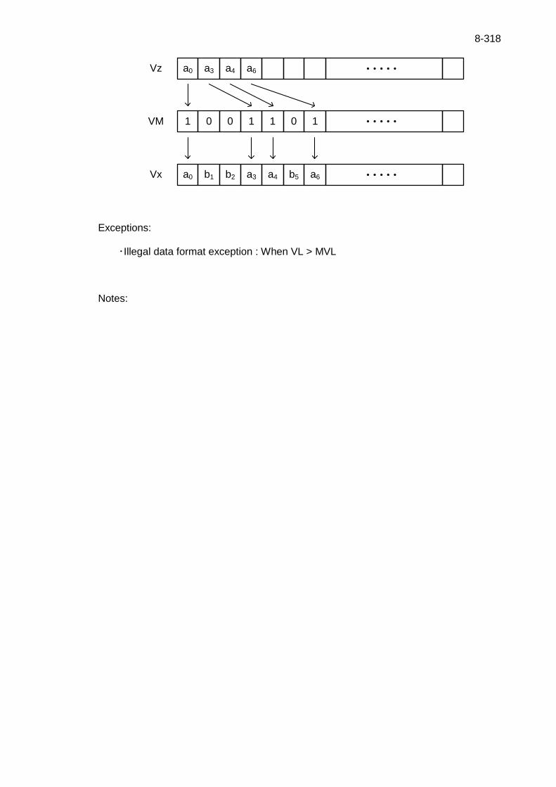
8-318
a0
Vz
b1 b2 a3 a4 b5 a6
1 0 0 1 1 0 1
a0 a3 a4 a6
VM
Vx
Exceptions:
・Illegal data format exception : When VL > MVL
Notes:
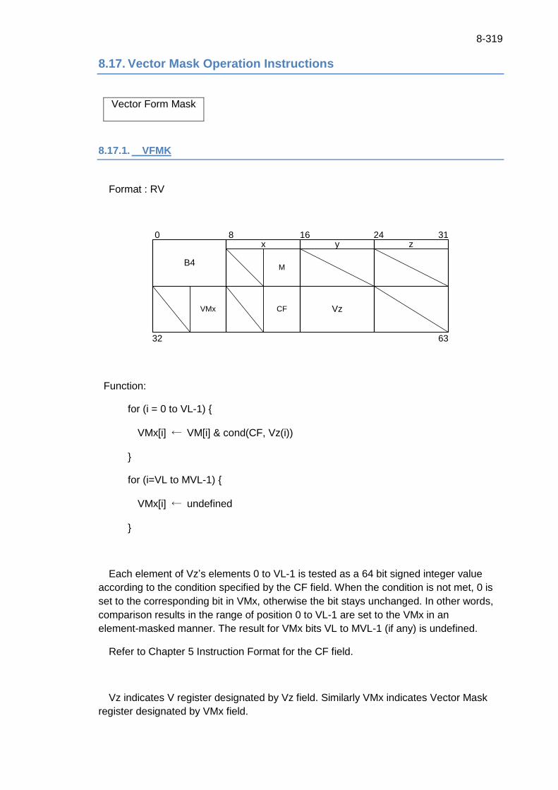
8-319
8.17. Vector Mask Operation Instructions
Vector Form Mask
8.17.1. VFMK
Format : RV
x
B4
y z8 16 24 31
32 63
0
Vz
M
VMx CF
Function:
for (i = 0 to VL-1) {
VMx[i] ← VM[i] & cond(CF, Vz(i))
}
for (i=VL to MVL-1) {
VMx[i] ← undefined
}
Each element of Vz’s elements 0 to VL-1 is tested as a 64 bit signed integer value
according to the condition specified by the CF field. When the condition is not met, 0 is
set to the corresponding bit in VMx, otherwise the bit stays unchanged. In other words,
comparison results in the range of position 0 to VL-1 are set to the VMx in an
element-masked manner. The result for VMx bits VL to MVL-1 (if any) is undefined.
Refer to Chapter 5 Instruction Format for the CF field.
Vz indicates V register designated by Vz field. Similarly VMx indicates Vector Mask
register designated by VMx field.

8-320
This operation on VM0 does nothing.
Exceptions:
・Illegal data format exception : When VL > MVL
Notes:
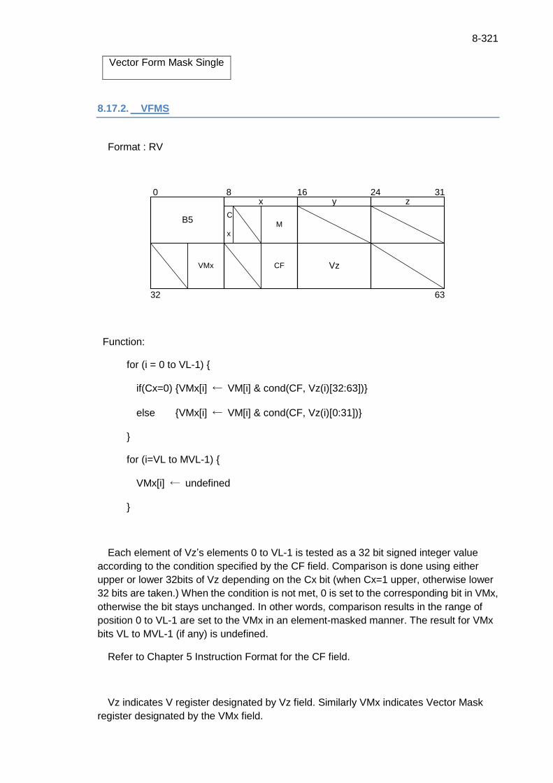
8-321
Vector Form Mask Single
8.17.2. VFMS
Format : RV
x
B5
y z8 16 24 31
32 63
0
Vz
M
VMx CF
C
x
Function:
for (i = 0 to VL-1) {
if(Cx=0) {VMx[i] ← VM[i] & cond(CF, Vz(i)[32:63])}
else {VMx[i] ← VM[i] & cond(CF, Vz(i)[0:31])}
}
for (i=VL to MVL-1) {
VMx[i] ← undefined
}
Each element of Vz’s elements 0 to VL-1 is tested as a 32 bit signed integer value
according to the condition specified by the CF field. Comparison is done using either
upper or lower 32bits of Vz depending on the Cx bit (when Cx=1 upper, otherwise lower
32 bits are taken.) When the condition is not met, 0 is set to the corresponding bit in VMx,
otherwise the bit stays unchanged. In other words, comparison results in the range of
position 0 to VL-1 are set to the VMx in an element-masked manner. The result for VMx
bits VL to MVL-1 (if any) is undefined.
Refer to Chapter 5 Instruction Format for the CF field.
Vz indicates V register designated by Vz field. Similarly VMx indicates Vector Mask
register designated by the VMx field.

8-322
This operation on VM0 does nothing.
Exceptions:
・Illegal data format exception : When VL > MVL
Notes:
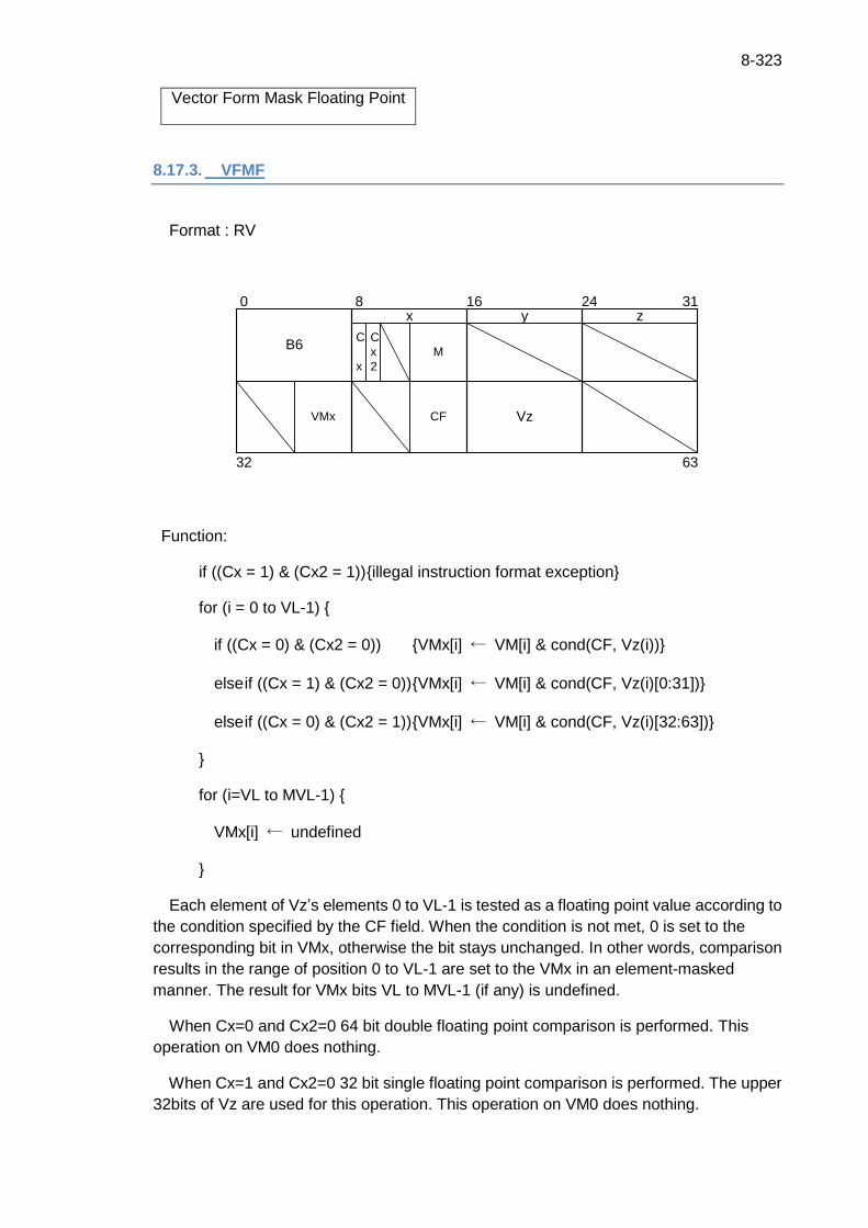
8-323
Vector Form Mask Floating Point
8.17.3. VFMF
Format : RV
x
B6
y z8 16 24 31
32 63
0
Vz
C
x
M
VMx CF
C
x
2
Function:
if ((Cx = 1) & (Cx2 = 1)) {illegal instruction format exception}
for (i = 0 to VL-1) {
if ((Cx = 0) & (Cx2 = 0)) {VMx[i] ← VM[i] & cond(CF, Vz(i))}
else if ((Cx = 1) & (Cx2 = 0)) {VMx[i] ← VM[i] & cond(CF, Vz(i)[0:31])}
else if ((Cx = 0) & (Cx2 = 1)) {VMx[i] ← VM[i] & cond(CF, Vz(i)[32:63])}
}
for (i=VL to MVL-1) {
VMx[i] ← undefined
}
Each element of Vz’s elements 0 to VL-1 is tested as a floating point value according to
the condition specified by the CF field. When the condition is not met, 0 is set to the
corresponding bit in VMx, otherwise the bit stays unchanged. In other words, comparison
results in the range of position 0 to VL-1 are set to the VMx in an element-masked
manner. The result for VMx bits VL to MVL-1 (if any) is undefined.
When Cx=0 and Cx2=0 64 bit double floating point comparison is performed. This
operation on VM0 does nothing.
When Cx=1 and Cx2=0 32 bit single floating point comparison is performed. The upper
32bits of Vz are used for this operation. This operation on VM0 does nothing.
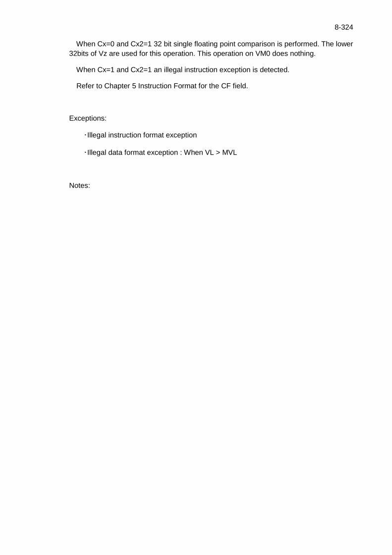
8-324
When Cx=0 and Cx2=1 32 bit single floating point comparison is performed. The lower
32bits of Vz are used for this operation. This operation on VM0 does nothing.
When Cx=1 and Cx2=1 an illegal instruction exception is detected.
Refer to Chapter 5 Instruction Format for the CF field.
Exceptions:
・Illegal instruction format exception
・Illegal data format exception : When VL > MVL
Notes:
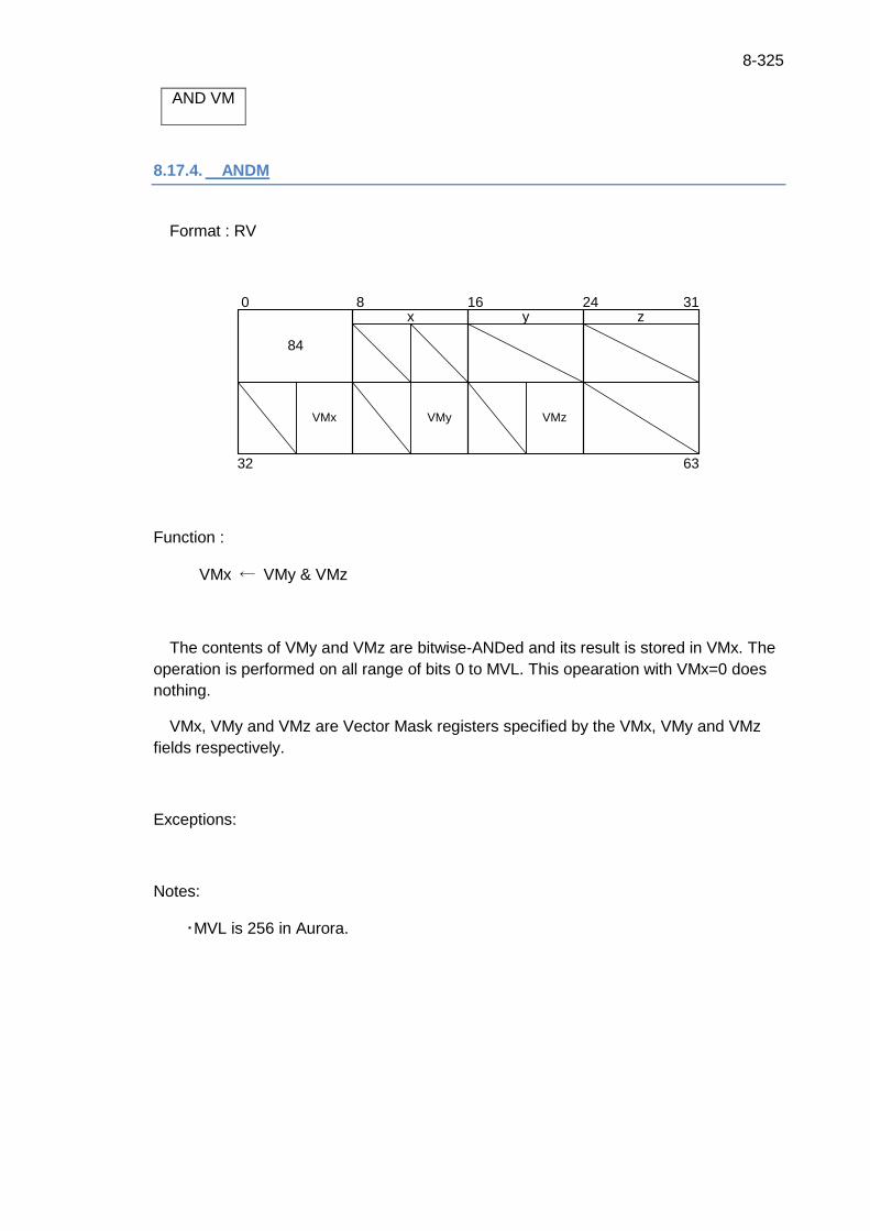
8-325
AND VM
8.17.4. ANDM
Format : RV
x
84
y z8 16 24 31
32 63
0
VMx VMy VMz
Function :
VMx ← VMy & VMz
The contents of VMy and VMz are bitwise-ANDed and its result is stored in VMx. The
operation is performed on all range of bits 0 to MVL. This opearation with VMx=0 does
nothing.
VMx, VMy and VMz are Vector Mask registers specified by the VMx, VMy and VMz
fields respectively.
Exceptions:
Notes:
・MVL is 256 in Aurora.
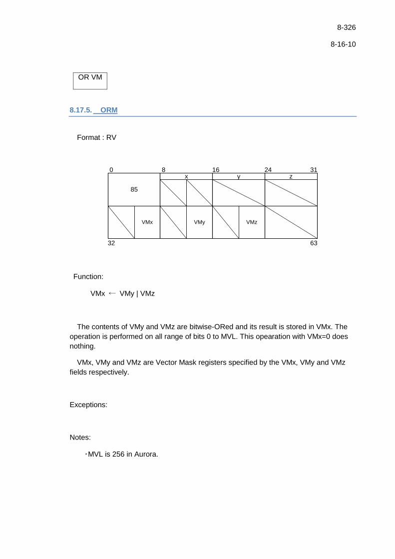
8-326
8-16-10
OR VM
8.17.5. ORM
Format : RV
x
85
y z8 16 24 31
32 63
0
VMx VMy VMz
Function:
VMx ← VMy | VMz
The contents of VMy and VMz are bitwise-ORed and its result is stored in VMx. The
operation is performed on all range of bits 0 to MVL. This opearation with VMx=0 does
nothing.
VMx, VMy and VMz are Vector Mask registers specified by the VMx, VMy and VMz
fields respectively.
Exceptions:
Notes:
・MVL is 256 in Aurora.
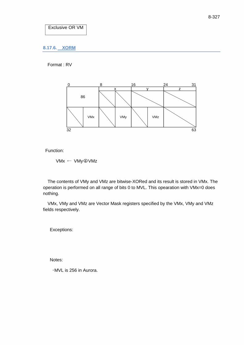
8-327
Exclusive OR VM
8.17.6. XORM
Format : RV
x
86
y z8 16 24 31
32 63
0
VMx VMy VMz
Function:
VMx ← VMy + VMz
The contents of VMy and VMz are bitwise-XORed and its result is stored in VMx. The
operation is performed on all range of bits 0 to MVL. This opearation with VMx=0 does
nothing.
VMx, VMy and VMz are Vector Mask registers specified by the VMx, VMy and VMz
fields respectively.
Exceptions:
Notes:
・MVL is 256 in Aurora.
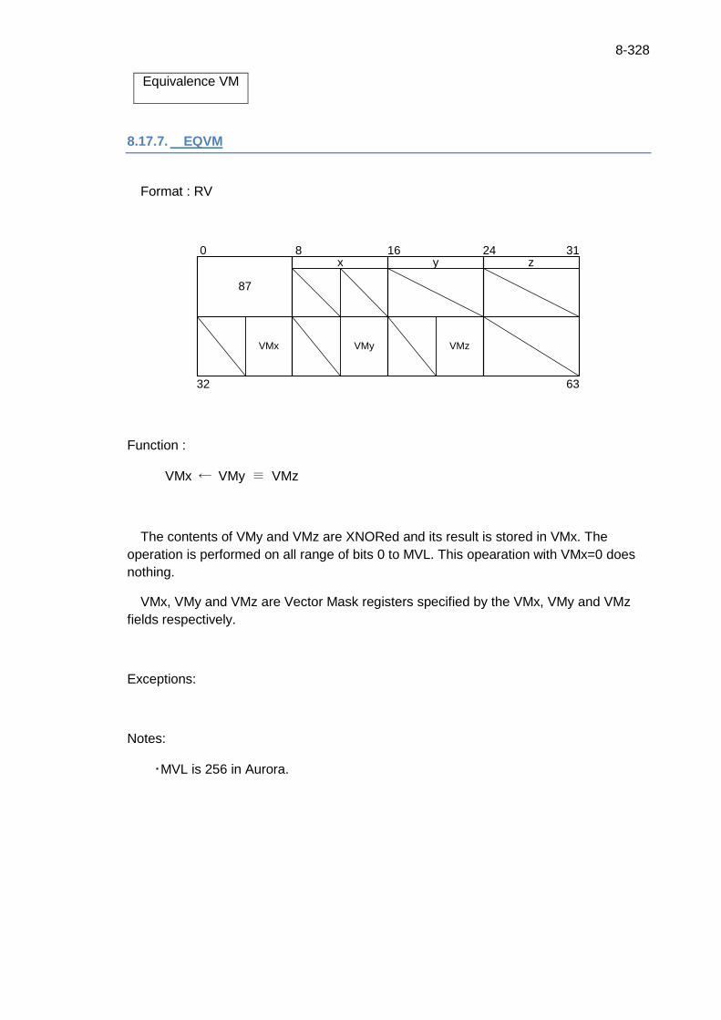
8-328
Equivalence VM
8.17.7. EQVM
Format : RV
x
87
y z8 16 24 31
32 63
0
VMx VMy VMz
Function :
VMx ← VMy ≡ VMz
The contents of VMy and VMz are XNORed and its result is stored in VMx. The
operation is performed on all range of bits 0 to MVL. This opearation with VMx=0 does
nothing.
VMx, VMy and VMz are Vector Mask registers specified by the VMx, VMy and VMz
fields respectively.
Exceptions:
Notes:
・MVL is 256 in Aurora.
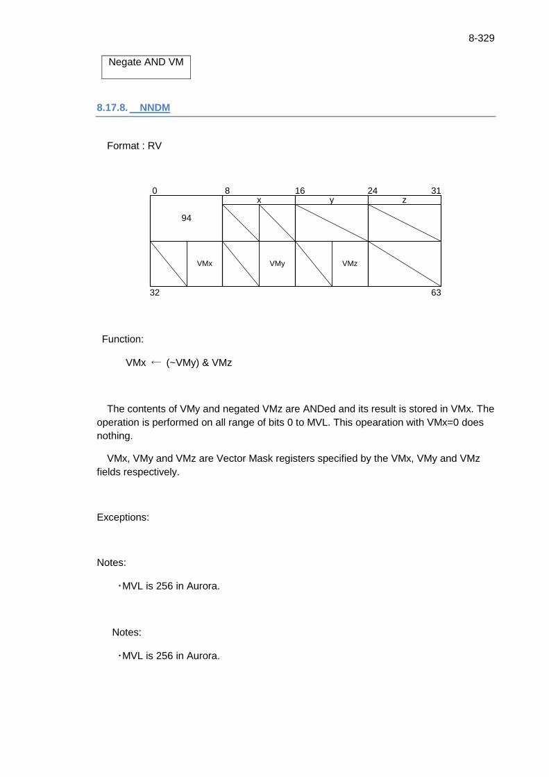
8-329
Negate AND VM
8.17.8. NNDM
Format : RV
x
94
y z8 16 24 31
32 63
0
VMx VMy VMz
Function:
VMx ← (~VMy) & VMz
The contents of VMy and negated VMz are ANDed and its result is stored in VMx. The
operation is performed on all range of bits 0 to MVL. This opearation with VMx=0 does
nothing.
VMx, VMy and VMz are Vector Mask registers specified by the VMx, VMy and VMz
fields respectively.
Exceptions:
Notes:
・MVL is 256 in Aurora.
Notes:
・MVL is 256 in Aurora.
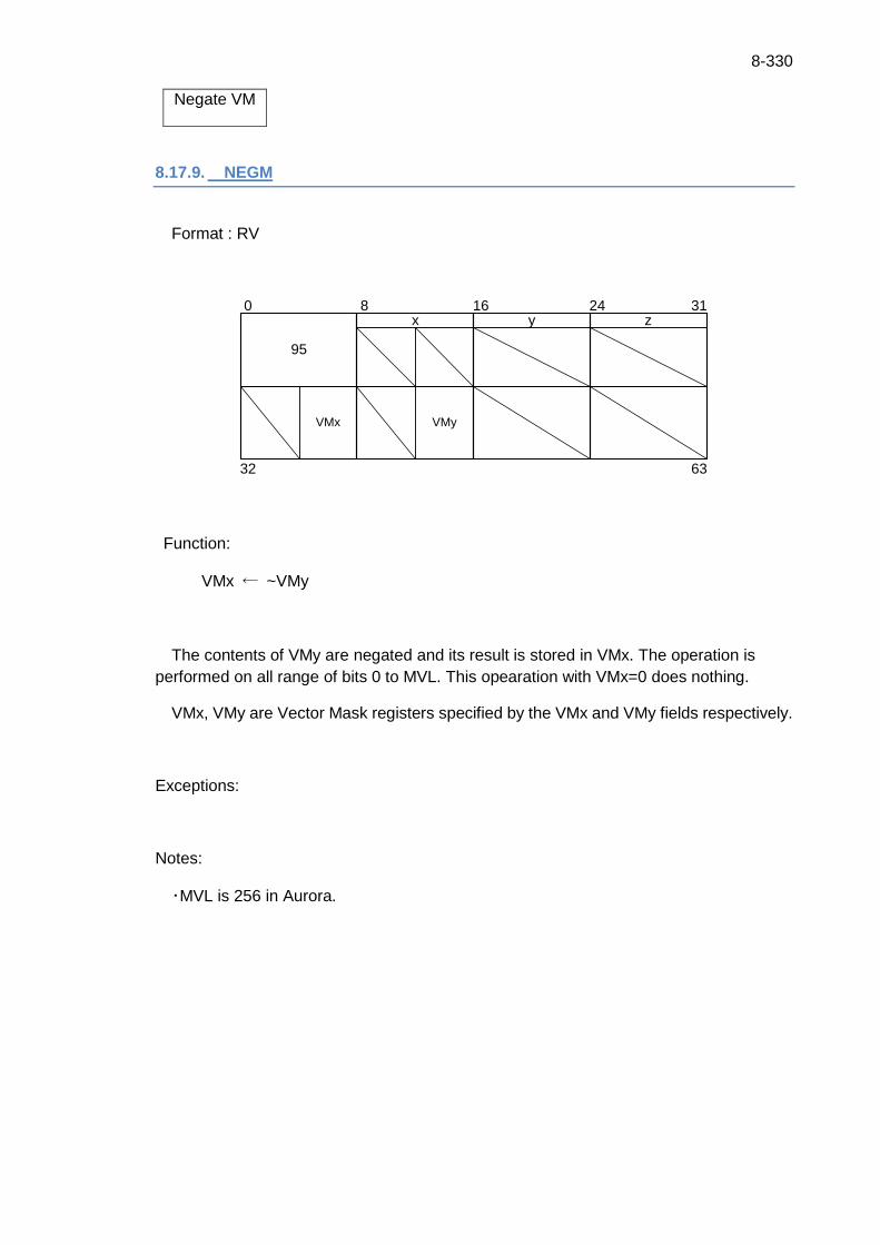
8-330
Negate VM
8.17.9. NEGM
Format : RV
x
95
y z8 16 24 31
32 63
0
VMx VMy
Function:
VMx ← ~VMy
The contents of VMy are negated and its result is stored in VMx. The operation is
performed on all range of bits 0 to MVL. This opearation with VMx=0 does nothing.
VMx, VMy are Vector Mask registers specified by the VMx and VMy fields respectively.
Exceptions:
Notes:
・MVL is 256 in Aurora.
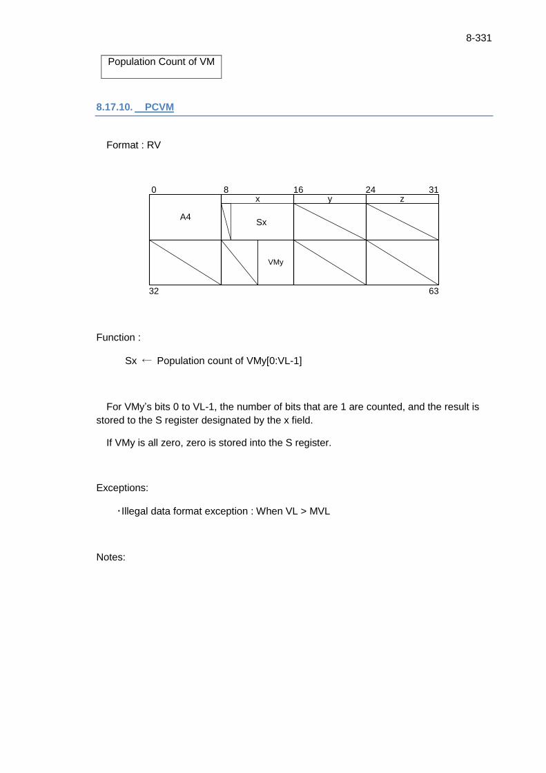
8-331
Population Count of VM
8.17.10. PCVM
Format : RV
x
A4
y z8 16 24 31
32 63
0
Sx
VMy
Function :
Sx ← Population count of VMy[0:VL-1]
For VMy’s bits 0 to VL-1, the number of bits that are 1 are counted, and the result is
stored to the S register designated by the x field.
If VMy is all zero, zero is stored into the S register.
Exceptions:
・Illegal data format exception : When VL > MVL
Notes:
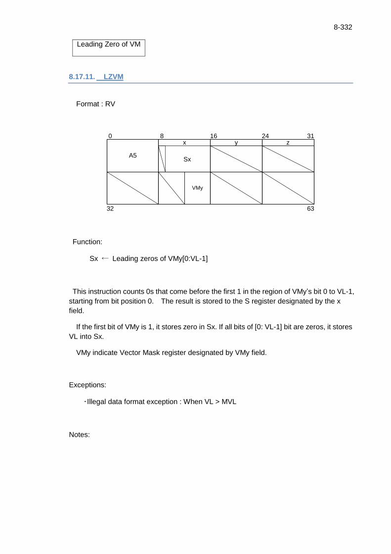
8-332
Leading Zero of VM
8.17.11. LZVM
Format : RV
x
A5
y z8 16 24 31
32 63
0
Sx
VMy
Function:
Sx ← Leading zeros of VMy[0:VL-1]
This instruction counts 0s that come before the first 1 in the region of VMy’s bit 0 to VL-1,
starting from bit position 0. The result is stored to the S register designated by the x
field.
If the first bit of VMy is 1, it stores zero in Sx. If all bits of [0: VL-1] bit are zeros, it stores
VL into Sx.
VMy indicate Vector Mask register designated by VMy field.
Exceptions:
・Illegal data format exception : When VL > MVL
Notes:
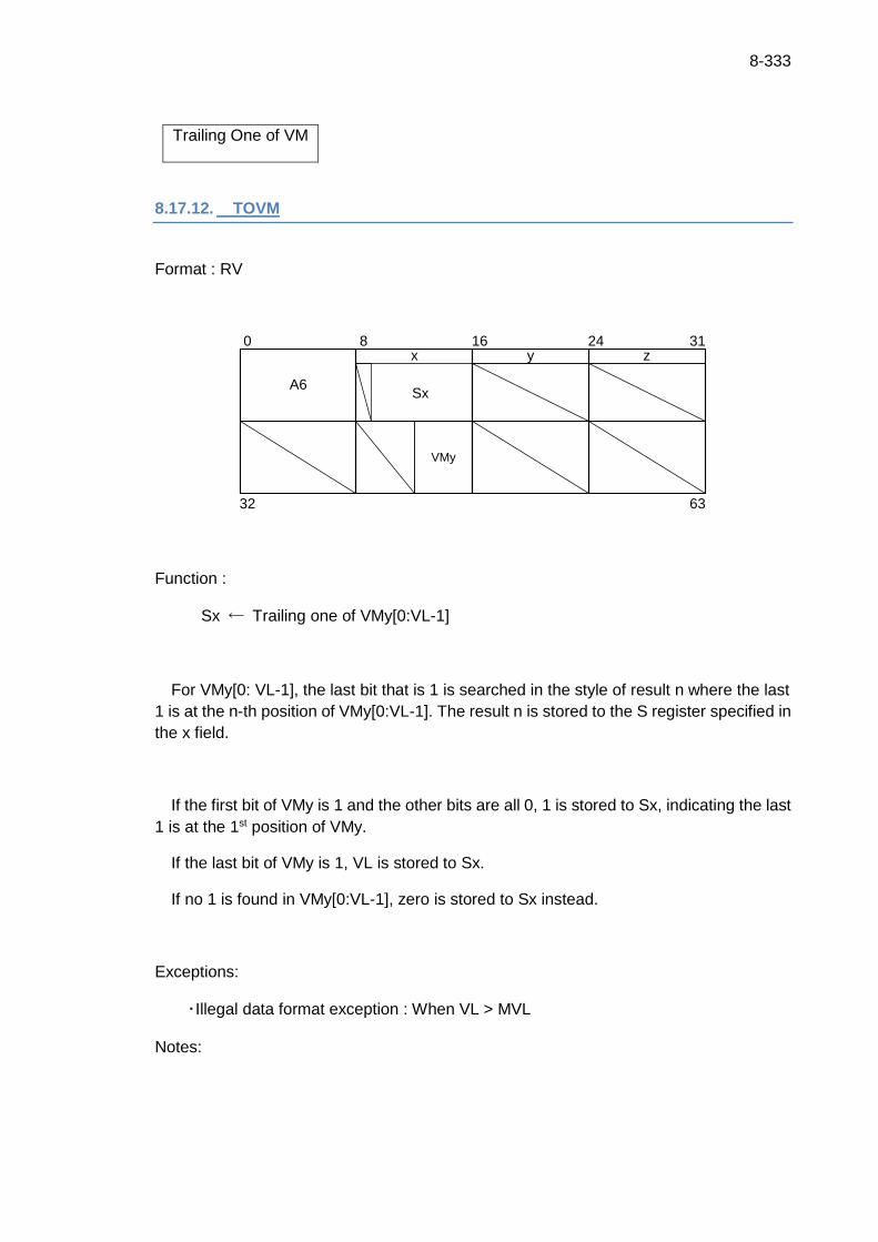
8-333
Trailing One of VM
8.17.12. TOVM
Format : RV
x
A6
y z8 16 24 31
32 63
0
Sx
VMy
Function :
Sx ← Trailing one of VMy[0:VL-1]
For VMy[0: VL-1], the last bit that is 1 is searched in the style of result n where the last
1 is at the n-th position of VMy[0:VL-1]. The result n is stored to the S register specified in
the x field.
If the first bit of VMy is 1 and the other bits are all 0, 1 is stored to Sx, indicating the last
1 is at the 1st position of VMy.
If the last bit of VMy is 1, VL is stored to Sx.
If no 1 is found in VMy[0:VL-1], zero is stored to Sx instead.
Exceptions:
・Illegal data format exception : When VL > MVL
Notes:
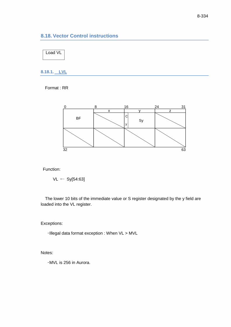
8-334
8.18. Vector Control instructions
Load VL
8.18.1. LVL
Format : RR
x
BF Sy
y
C
y
z8 16 24 31
32 63
0
Function:
VL ← Sy[54:63]
The lower 10 bits of the immediate value or S register designated by the y field are
loaded into the VL register.
Exceptions:
・Illegal data format exception : When VL > MVL
Notes:
・MVL is 256 in Aurora.
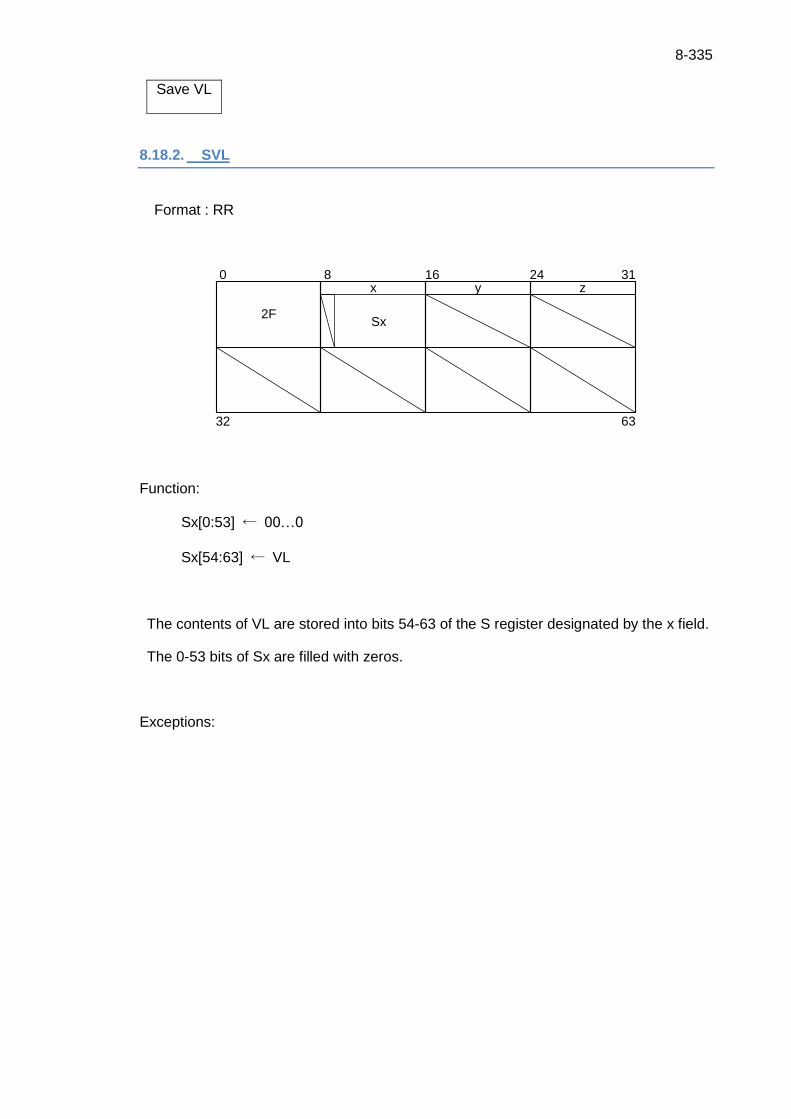
8-335
Save VL
8.18.2. SVL
Format : RR
x
2F
y z8 16 24 31
32 63
0
Sx
Function:
Sx[0:53] ← 00…0
Sx[54:63] ← VL
The contents of VL are stored into bits 54-63 of the S register designated by the x field.
The 0-53 bits of Sx are filled with zeros.
Exceptions:
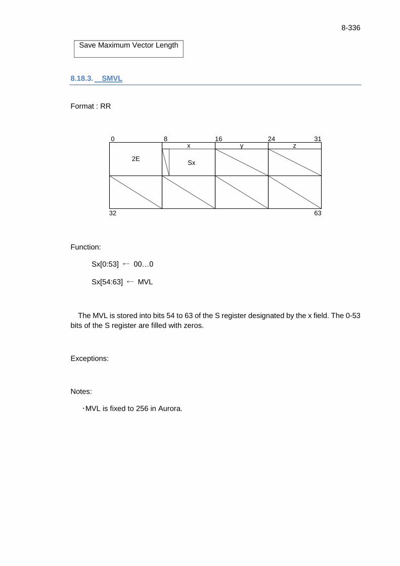
8-336
Save Maximum Vector Length
8.18.3. SMVL
Format : RR
x
2E
y z8 16 24 31
32 63
0
Sx
Function:
Sx[0:53] ← 00…0
Sx[54:63] ← MVL
The MVL is stored into bits 54 to 63 of the S register designated by the x field. The 0-53
bits of the S register are filled with zeros.
Exceptions:
Notes:
・MVL is fixed to 256 in Aurora.
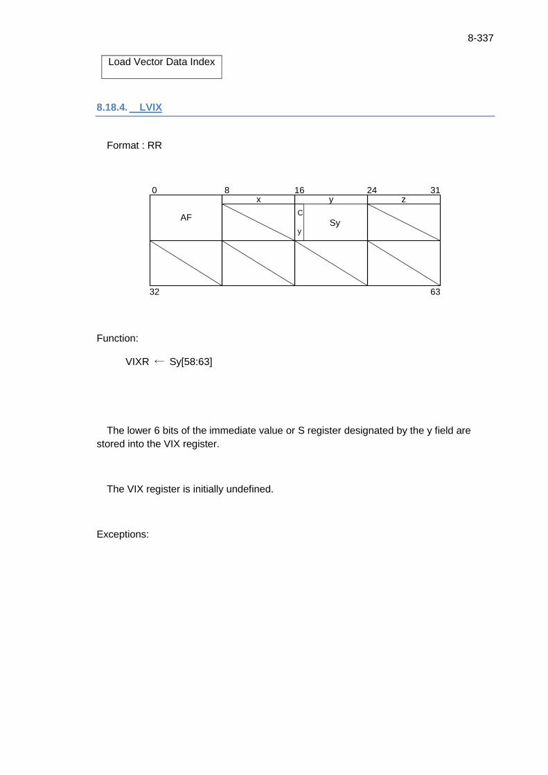
8-337
Load Vector Data Index
8.18.4. LVIX
Format : RR
x
AF Sy
y
C
y
z8 16 24 31
32 63
0
Function:
VIXR ← Sy[58:63]
The lower 6 bits of the immediate value or S register designated by the y field are
stored into the VIX register.
The VIX register is initially undefined.
Exceptions:
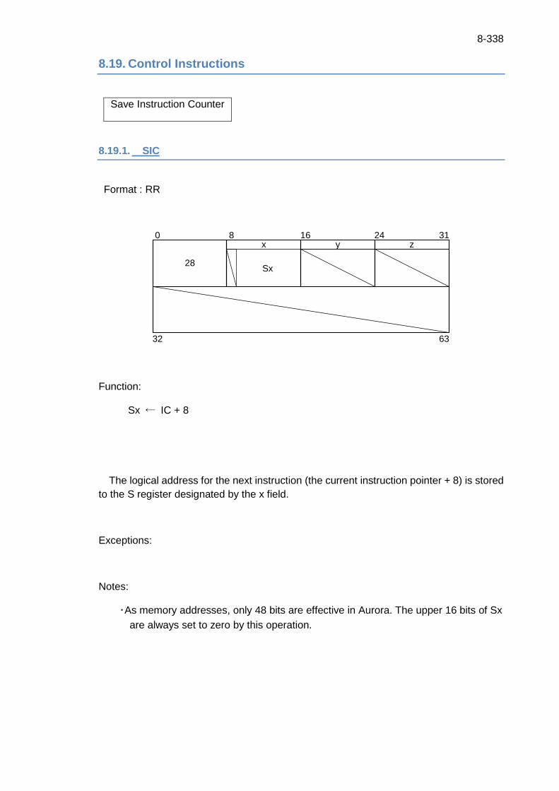
8-338
8.19. Control Instructions
Save Instruction Counter
8.19.1. SIC
Format : RR
x
28 Sx
y z8 16 24 31
32 63
0
Function:
Sx ← IC + 8
The logical address for the next instruction (the current instruction pointer + 8) is stored
to the S register designated by the x field.
Exceptions:
Notes:
・As memory addresses, only 48 bits are effective in Aurora. The upper 16 bits of Sx
are always set to zero by this operation.
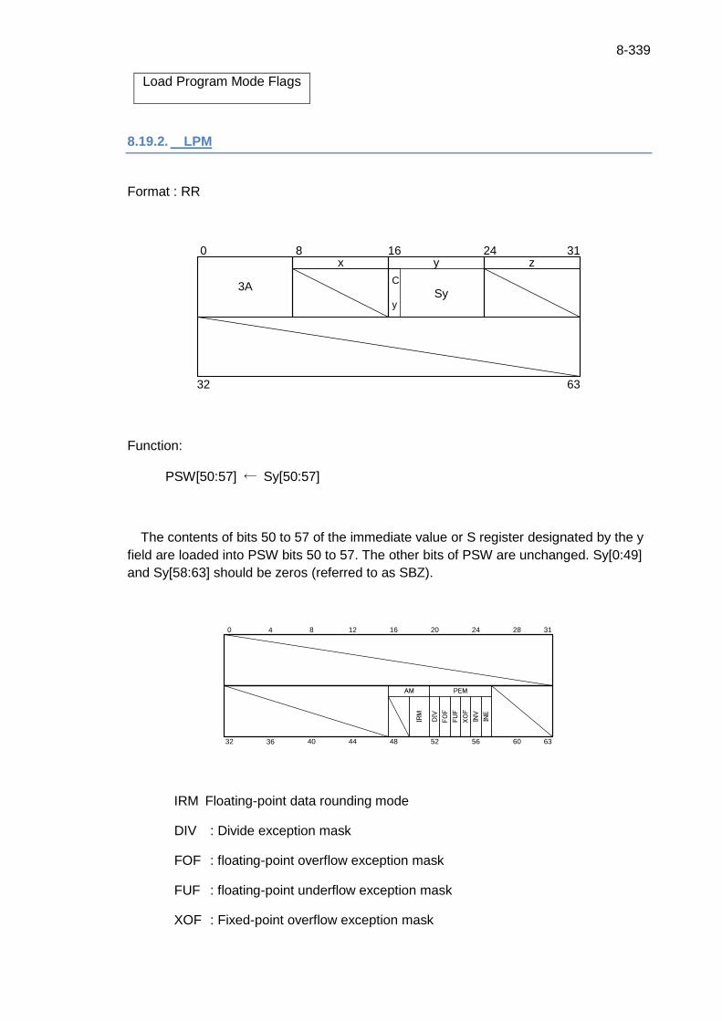
8-339
Load Program Mode Flags
8.19.2. LPM
Format : RR
x
3A Sy
y
C
y
z8 16 24 31
32 63
0
Function:
PSW[50:57] ← Sy[50:57]
The contents of bits 50 to 57 of the immediate value or S register designated by the y
field are loaded into PSW bits 50 to 57. The other bits of PSW are unchanged. Sy[0:49]
and Sy[58:63] should be zeros (referred to as SBZ).
0 4 8 12 16 20 24 28 31
DIV
FO
F
FU
F
XO
F
PEM
INV
INE
AM
IRM
32 36 40 44 48 52 56 60 63
IRM Floating-point data rounding mode
DIV : Divide exception mask
FOF : floating-point overflow exception mask
FUF : floating-point underflow exception mask
XOF : Fixed-point overflow exception mask

8-340
INV Invalid operation exception mask
INE Inexact exception mask
Exceptions:
Notes:
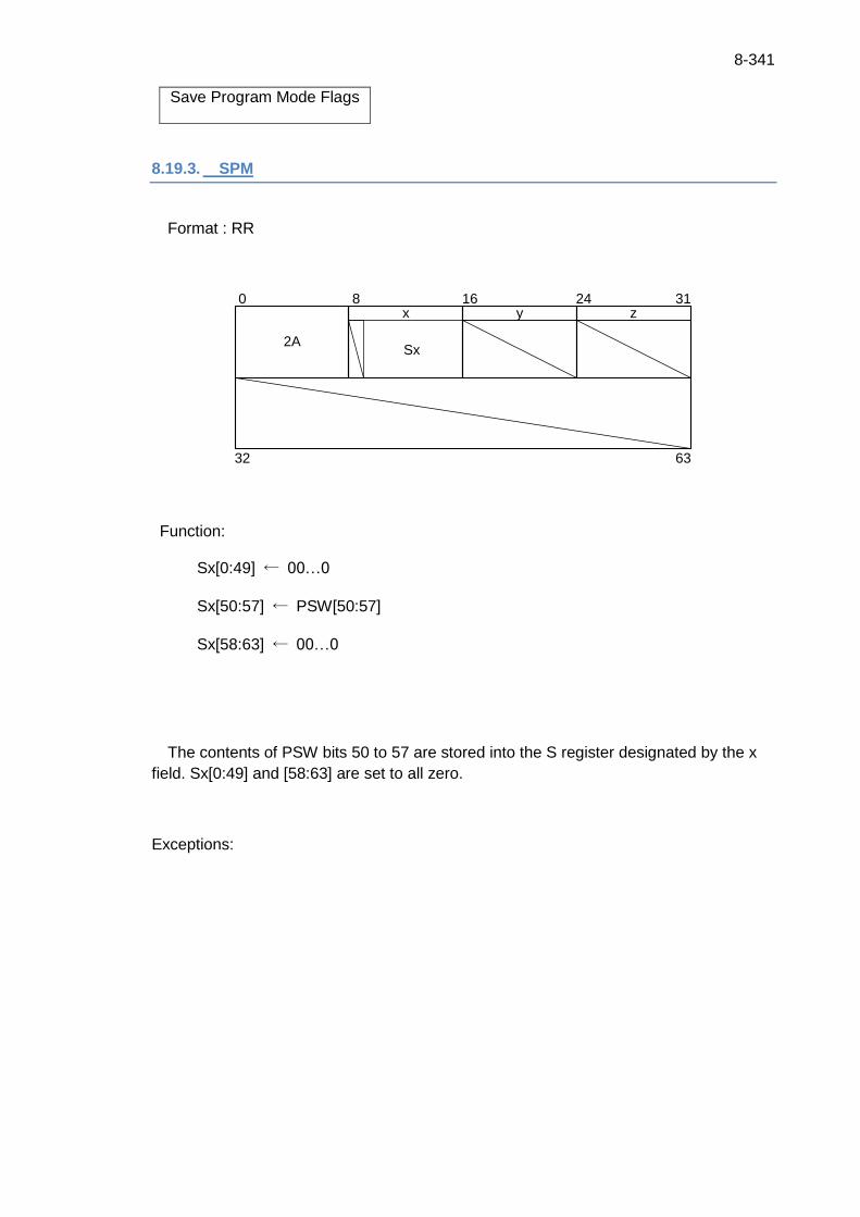
8-341
Save Program Mode Flags
8.19.3. SPM
Format : RR
x
2A Sx
y z8 16 24 31
32 63
0
Function:
Sx[0:49] ← 00…0
Sx[50:57] ← PSW[50:57]
Sx[58:63] ← 00…0
The contents of PSW bits 50 to 57 are stored into the S register designated by the x
field. Sx[0:49] and [58:63] are set to all zero.
Exceptions:
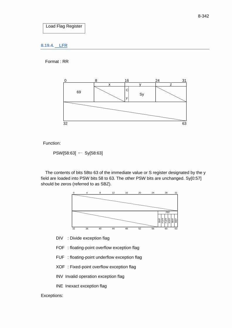
8-342
Load Flag Register
8.19.4. LFR
Format : RR
x
69 Sy
y
C
y
z8 16 24 31
32 63
0
Function:
PSW[58:63] ← Sy[58:63]
The contents of bits 58to 63 of the immediate value or S register designated by the y
field are loaded into PSW bits 58 to 63. The other PSW bits are unchanged. Sy[0:57]
should be zeros (referred to as SBZ).
0 4 8 12 16 20 24 28 31
DIV
F
FO
FF
FU
FF
XO
FF
PEF
INV
F
INEF
32 36 40 44 48 52 56 60 63
DIV : Divide exception flag
FOF : floating-point overflow exception flag
FUF : floating-point underflow exception flag
XOF : Fixed-point overflow exception flag
INV Invalid operation exception flag
INE Inexact exception flag
Exceptions:
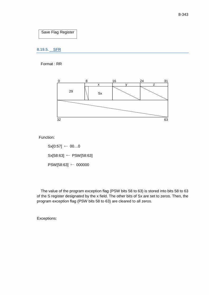
8-343
Save Flag Register
8.19.5. SFR
Format : RR
x
29 Sx
y z8 16 24 31
32 63
0
Function:
Sx[0:57] ← 00…0
Sx[58:63] ← PSW[58:63]
PSW[58:63] ← 000000
The value of the program exception flag (PSW bits 58 to 63) is stored into bits 58 to 63
of the S register designated by the x field. The other bits of Sx are set to zeros. Then, the
program exception flag (PSW bits 58 to 63) are cleared to all zeros.
Exceptions:
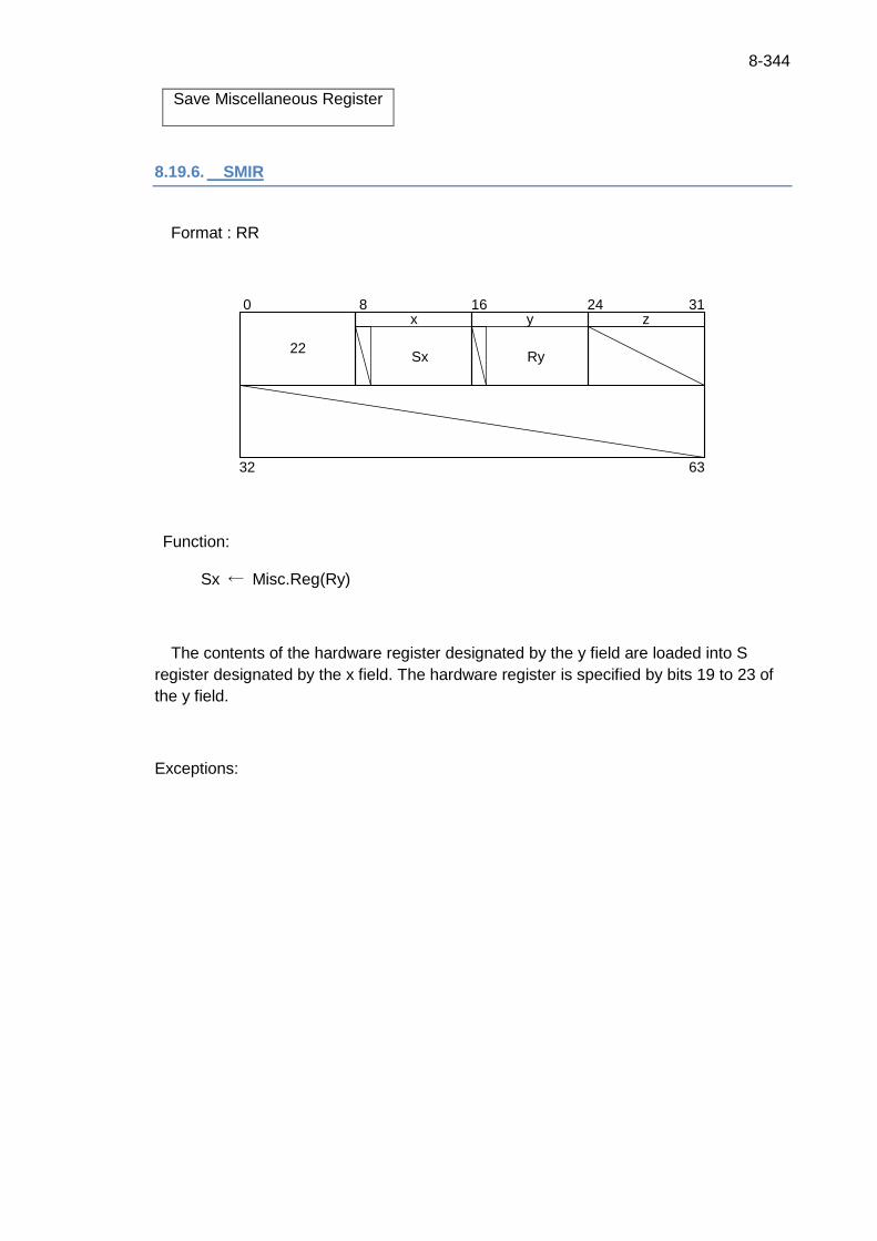
8-344
Save Miscellaneous Register
8.19.6. SMIR
Format : RR
x
22 Sx Ry
y z8 16 24 31
32 63
0
Function:
Sx ← Misc.Reg(Ry)
The contents of the hardware register designated by the y field are loaded into S
register designated by the x field. The hardware register is specified by bits 19 to 23 of
the y field.
Exceptions:
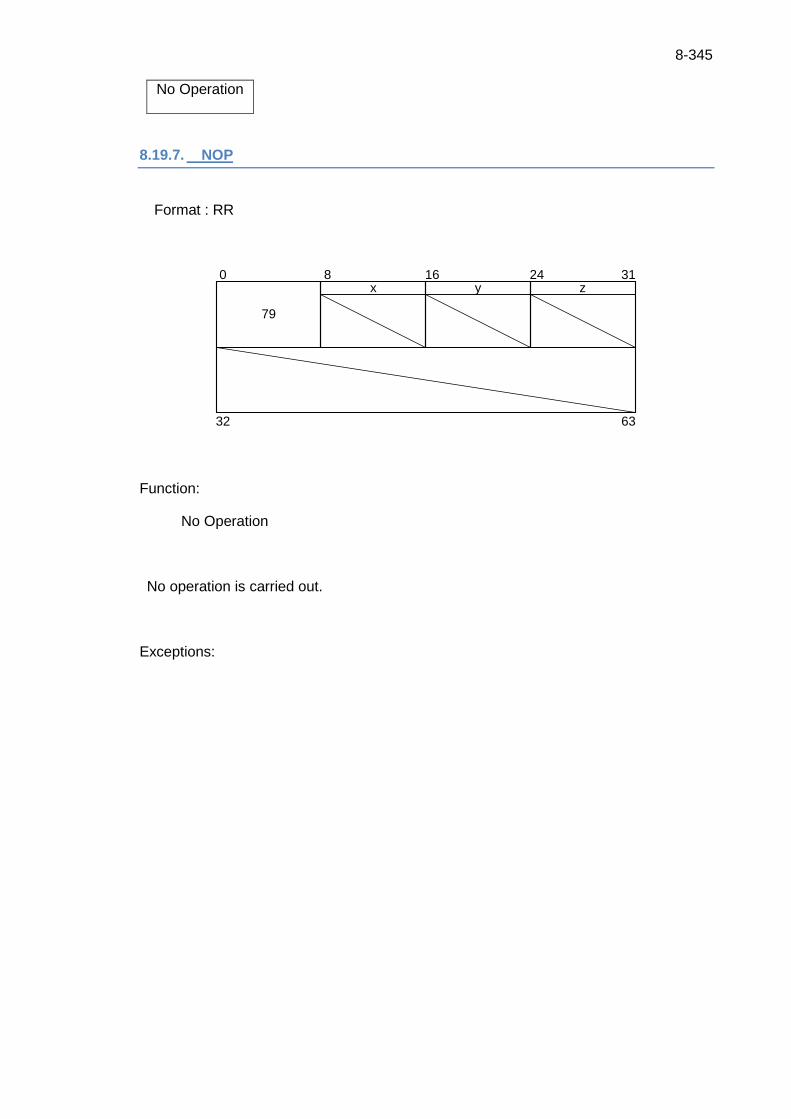
8-345
No Operation
8.19.7. NOP
Format : RR
x
79
y z8 16 24 31
32 63
0
Function:
No Operation
No operation is carried out.
Exceptions:
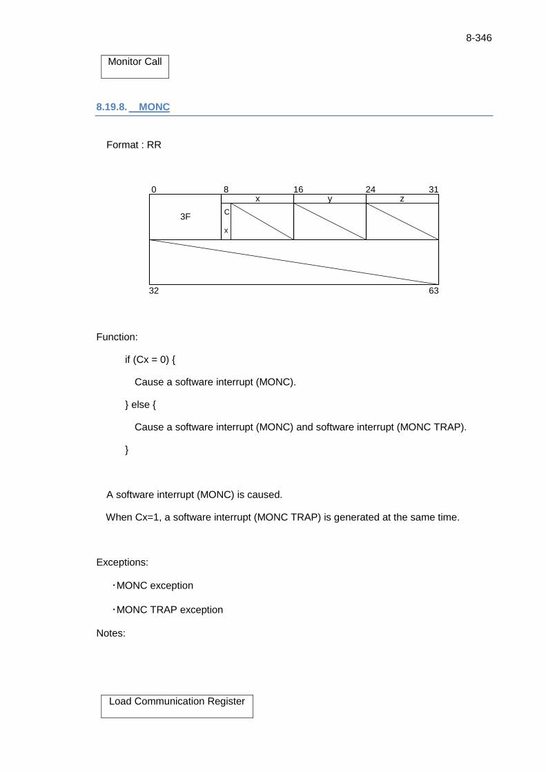
8-346
Monitor Call
8.19.8. MONC
Format : RR
x
3F
y z8 16 24 31
32 63
0
C
x
Function:
if (Cx = 0) {
Cause a software interrupt (MONC).
} else {
Cause a software interrupt (MONC) and software interrupt (MONC TRAP).
}
A software interrupt (MONC) is caused.
When Cx=1, a software interrupt (MONC TRAP) is generated at the same time.
Exceptions:
・MONC exception
・MONC TRAP exception
Notes:
Load Communication Register
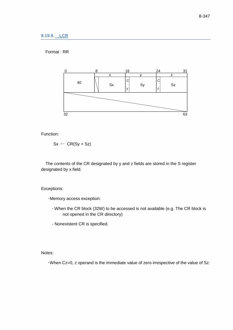
8-347
8.19.9. LCR
Format : RR
x
40 Sx Sy Sz
y
C
y
z
C
z
8 16 24 31
32 63
0
Function:
Sx ← CR(Sy + Sz)
The contents of the CR designated by y and z fields are stored in the S register
designated by x field.
Exceptions:
・Memory access exception:
- When the CR block (32W) to be accessed is not available (e.g. The CR block is
not opened in the CR directory)
- Nonexistent CR is specified.
Notes:
・When Cz=0, z operand is the immediate value of zero irrespective of the value of Sz.
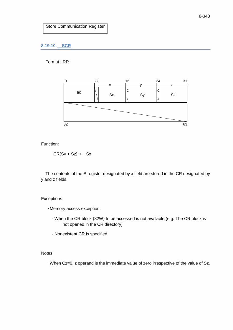
8-348
Store Communication Register
8.19.10. SCR
Format : RR
x
50 Sx Sy Sz
y
C
y
z
C
z
8 16 24 31
32 63
0
Function:
CR(Sy + Sz) ← Sx
The contents of the S register designated by x field are stored in the CR designated by
y and z fields.
Exceptions:
・Memory access exception:
- When the CR block (32W) to be accessed is not available (e.g. The CR block is
not opened in the CR directory)
- Nonexistent CR is specified.
Notes:
・When Cz=0, z operand is the immediate value of zero irrespective of the value of Sz.
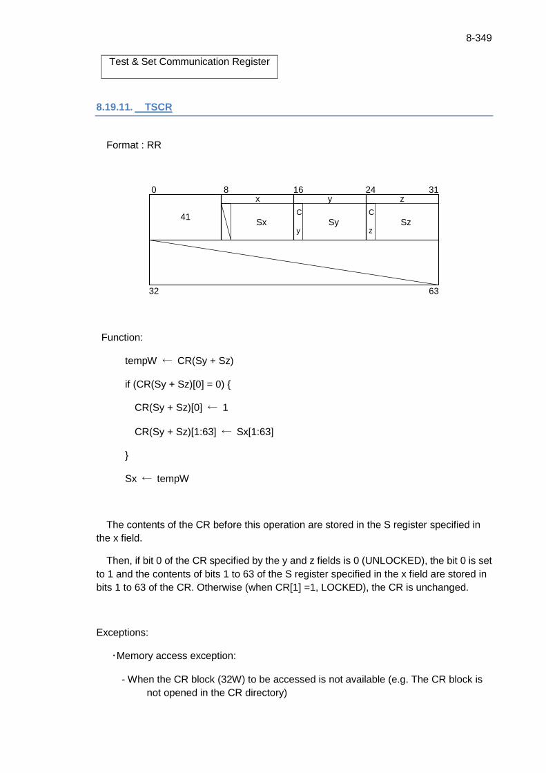
8-349
Test & Set Communication Register
8.19.11. TSCR
Format : RR
x
41 Sx Sy Sz
y
C
y
z
C
z
8 16 24 31
32 63
0
Function:
tempW ← CR(Sy + Sz)
if (CR(Sy + Sz)[0] = 0) {
CR(Sy + Sz)[0] ← 1
CR(Sy + Sz)[1:63] ← Sx[1:63]
}
Sx ← tempW
The contents of the CR before this operation are stored in the S register specified in
the x field.
Then, if bit 0 of the CR specified by the y and z fields is 0 (UNLOCKED), the bit 0 is set
to 1 and the contents of bits 1 to 63 of the S register specified in the x field are stored in
bits 1 to 63 of the CR. Otherwise (when CR[1] =1, LOCKED), the CR is unchanged.
Exceptions:
・Memory access exception:
- When the CR block (32W) to be accessed is not available (e.g. The CR block is
not opened in the CR directory)
8-350
- Nonexistent CR is specified.
Notes:
・When Cz=0, z operand is the immediate value of zero irrespective of the value of Sz.
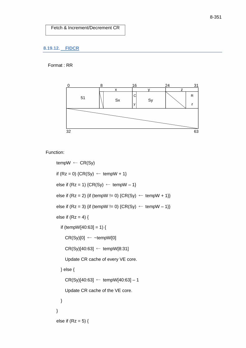
8-351
Fetch & Increment/Decrement CR
8.19.12. FIDCR
Format : RR
x
51 Sx Sy
y
C
y
z
R
z
8 16 24 31
32 63
0
Function:
tempW ← CR(Sy)
if (Rz = 0) {CR(Sy) ← tempW + 1}
else if (Rz = 1) {CR(Sy) ← tempW – 1}
else if (Rz = 2) {if (tempW != 0) {CR(Sy) ← tempW + 1}}
else if (Rz = 3) {if (tempW != 0) {CR(Sy) ← tempW – 1}}
else if (Rz = 4) {
if (tempW[40:63] = 1) {
CR(Sy)[0] ← ~tempW[0]
CR(Sy)[40:63] ← tempW[8:31]
Update CR cache of every VE core.
} else {
CR(Sy)[40:63] ← tempW[40:63] – 1
Update CR cache of the VE core.
}
}
else if (Rz = 5) {
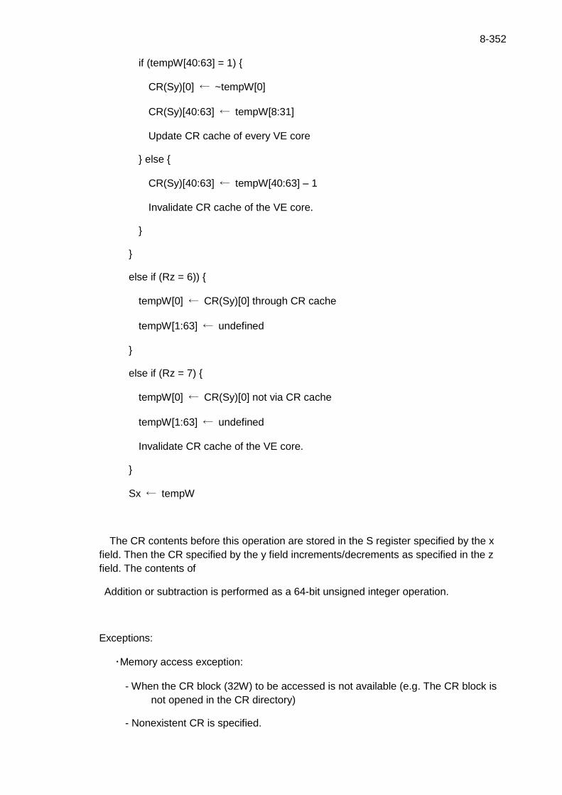
8-352
if (tempW[40:63] = 1) {
CR(Sy)[0] ← ~tempW[0]
CR(Sy)[40:63] ← tempW[8:31]
Update CR cache of every VE core
} else {
CR(Sy)[40:63] ← tempW[40:63] – 1
Invalidate CR cache of the VE core.
}
}
else if (Rz = 6)) {
tempW[0] ← CR(Sy)[0] through CR cache
tempW[1:63] ← undefined
}
else if (Rz = 7) {
tempW[0] ← CR(Sy)[0] not via CR cache
tempW[1:63] ← undefined
Invalidate CR cache of the VE core.
}
Sx ← tempW
The CR contents before this operation are stored in the S register specified by the x
field. Then the CR specified by the y field increments/decrements as specified in the z
field. The contents of
Addition or subtraction is performed as a 64-bit unsigned integer operation.
Exceptions:
・Memory access exception:
- When the CR block (32W) to be accessed is not available (e.g. The CR block is
not opened in the CR directory)
- Nonexistent CR is specified.

8-353
Notes:
Unless the use of CR cache is explicitly intended by specifying Rz=4 or 6, processor
core accesses the CR bypassing the CR cache. Since the intended CR data may be
evicted from the CR cache by other accesses, software should take care not to incur
performance loss due to that.
8-354
8.20. Host Memory Access Instructions
Load Host Memory
8.20.1. LHM
Format : RRM
x
21 Sx Sz
y z
C
z
8 16 24 31
32 63
0
R
y
D
Function:
EA ← Sz + sext(D, 64)
Sx ← Host memory space(EA)
Data is loaded from the location in the VE host virtual address space addressed by the
z and D fields, to the S register designated by x field, in the size specified by the y field.
The transfer data size is as follows.
00:1byte
01:2byte
10:4byte
11:8byte
When the designated data size is less than 8 bytes, the load data is stored into lower
bytes of the S register designated by x field, and its sign bit is extended and stored into
higher bits of the S register.

8-355
The host memory address designated by z and D fields must be aligned to transfer
data size boundary. Otherwise memory access exception occurs.
Exceptions:
・Host missing page exception
・Host missing space exception
・Host memory access exception
・I/O Access exception
Notes:
・When Cz=0, z operand is the immediate value of zero irrespective of the value of
Sz.
8-356
Store Host Memory
8.20.2. SHM
Format : RRM
x
31 Sx Sz
y z
C
z
8 16 24 31
32 63
0
R
y
D
Function:
EA ← Sz + sext(D, 64)
Host memory space(EA) ← Sx
Sx is stored to the location in the VE host virtual address space addressed by the z and
D fields, in the size specified by the y field. The transfer data size is as follows.
The transfer data size is designated by 2 bits of Ry as follows.
00:1byte
01:2byte
10:4byte
11:8byte
When the designated data size is less than 8 byte, it is assumed the write data is
stored into lower bytes of S register designated by x field.
The host memory address designated by z and D fields must be aligned to transfer
data size boundary, otherwise memory access exception occurs.
8-357
Exceptions:
・Host memory protection exception
・Host missing page exception
・Host missing space exception
・Host memory access exception
Notes:
・When Cz=0, z operand is the immediate value of zero irrespective of the value of
Sz.
9. Appendix-1 Microarchitecture of SX-Aurora
TSUBASA
9.1. VE CPU
The Aurora VE CPU is the central processing component of the Aurora VE. The CPU
executes programs compiled for Aurora systems, holds data on its own memory and
communicates with other PCIe devices and the VE host.
Figure 9-1 shows a diagram of the VE CPU for SX-Aurora TSUABASA systems, For
SX-Aurora TSUBASA generation systems, the VE CPU contains eight VE cores, LLC
(Last level cache), MCU (Memory control unit) and DMU (DMA management unit), XIU
(AXI bus interface unit) and PEU (PCIe unit). It also has DGU (Diagnosis unit) and a ring
bus connecting DMU and LLCs.
The cores and LLCs are connected by a 2D mesh styled NoC (network on chip).
MCUs controls memory transaction to external HBMs (high bandwidth memory).
The Aurora VE has 6 HBMs on the interposer module, and the CPU has 6 MCUs as
their counterparts.
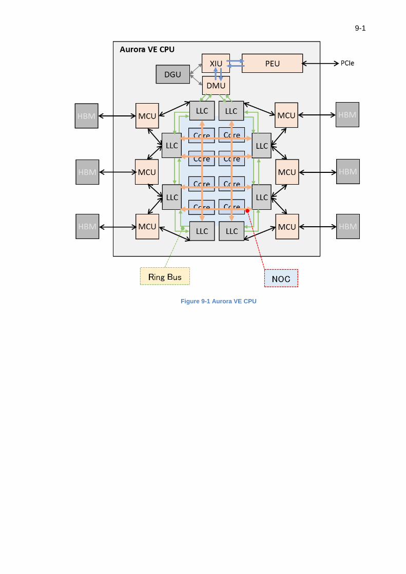
9-1
Figure 9-1 Aurora VE CPU
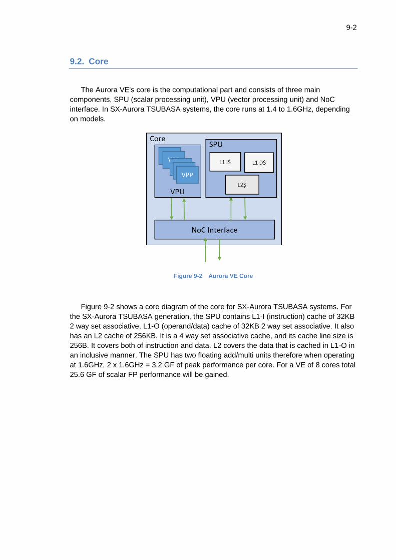
9-2
9.2. Core
The Aurora VE's core is the computational part and consists of three main
components, SPU (scalar processing unit), VPU (vector processing unit) and NoC
interface. In SX-Aurora TSUBASA systems, the core runs at 1.4 to 1.6GHz, depending
on models.
Figure 9-2 Aurora VE Core
Figure 9-2 shows a core diagram of the core for SX-Aurora TSUBASA systems. For
the SX-Aurora TSUBASA generation, the SPU contains L1-I (instruction) cache of 32KB
2 way set associative, L1-O (operand/data) cache of 32KB 2 way set associative. It also
has an L2 cache of 256KB. It is a 4 way set associative cache, and its cache line size is
256B. It covers both of instruction and data. L2 covers the data that is cached in L1-O in
an inclusive manner. The SPU has two floating add/multi units therefore when operating
at 1.6GHz, 2 x 1.6GHz = 3.2 GF of peak performance per core. For a VE of 8 cores total
25.6 GF of scalar FP performance will be gained.
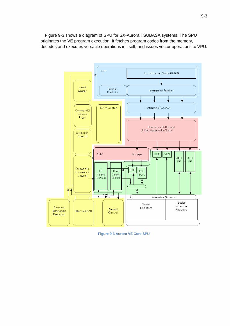
9-3
Figure 9-3 shows a diagram of SPU for SX-Aurora TSUBASA systems. The SPU
originates the VE program execution. It fetches program codes from the memory,
decodes and executes versatile operations in itself, and issues vector operations to VPU.
Figure 9-3 Aurora VE Core SPU
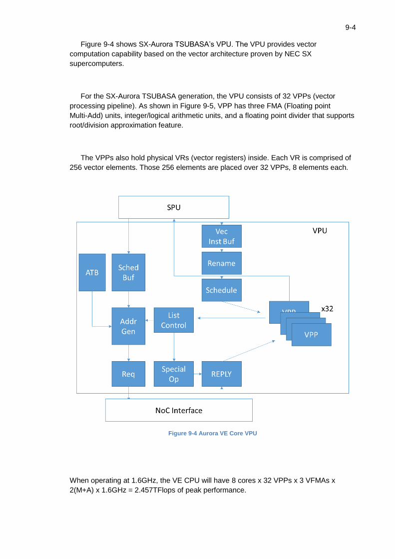
9-4
Figure 9-4 shows SX-Aurora TSUBASA’s VPU. The VPU provides vector
computation capability based on the vector architecture proven by NEC SX
supercomputers.
For the SX-Aurora TSUBASA generation, the VPU consists of 32 VPPs (vector
processing pipeline). As shown in Figure 9-5, VPP has three FMA (Floating point
Multi-Add) units, integer/logical arithmetic units, and a floating point divider that supports
root/division approximation feature.
The VPPs also hold physical VRs (vector registers) inside. Each VR is comprised of
256 vector elements. Those 256 elements are placed over 32 VPPs, 8 elements each.
Figure 9-4 Aurora VE Core VPU
When operating at 1.6GHz, the VE CPU will have 8 cores x 32 VPPs x 3 VFMAs x
2(M+A) x 1.6GHz = 2.457TFlops of peak performance.
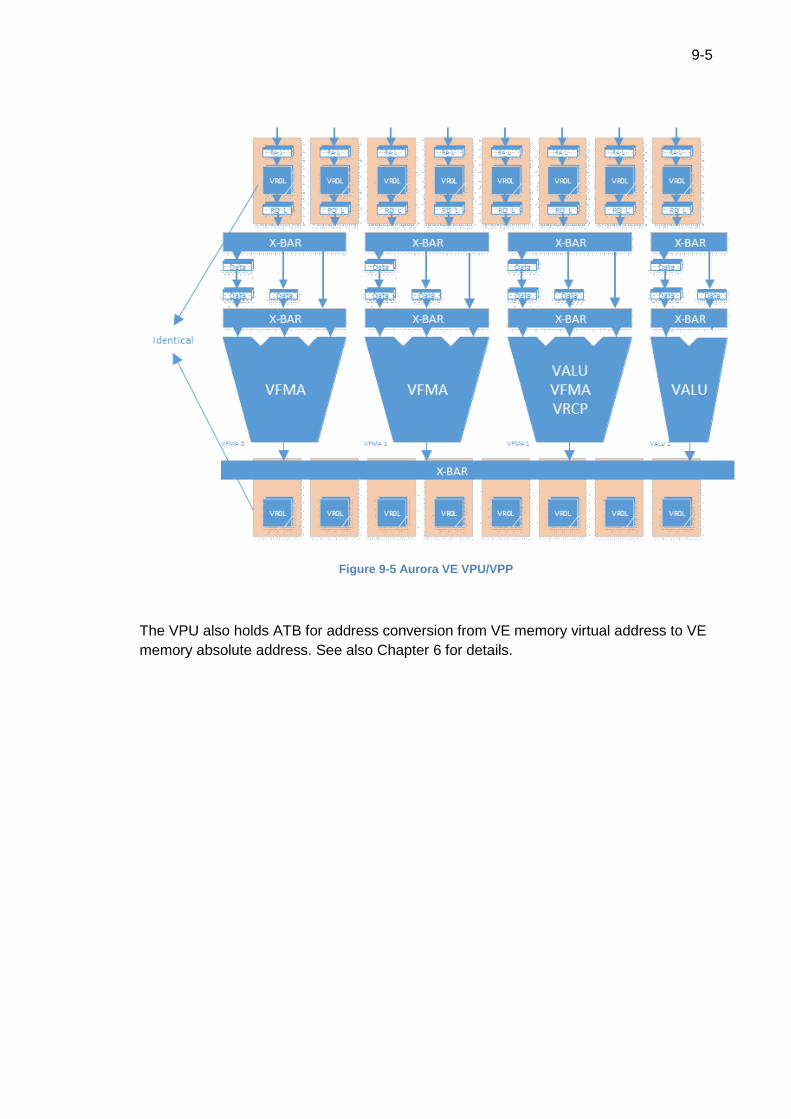
9-5
Figure 9-5 Aurora VE VPU/VPP
The VPU also holds ATB for address conversion from VE memory virtual address to VE
memory absolute address. See also Chapter 6 for details.
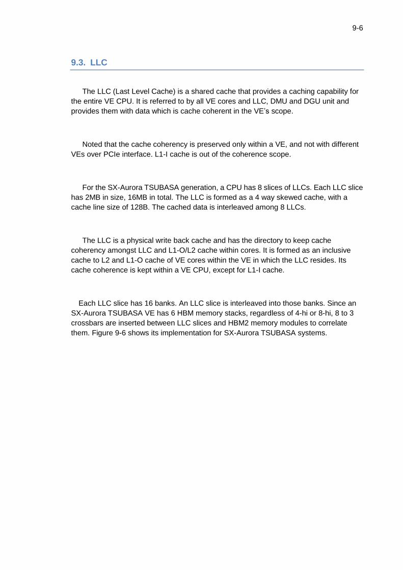
9-6
9.3. LLC
The LLC (Last Level Cache) is a shared cache that provides a caching capability for
the entire VE CPU. It is referred to by all VE cores and LLC, DMU and DGU unit and
provides them with data which is cache coherent in the VE’s scope.
Noted that the cache coherency is preserved only within a VE, and not with different
VEs over PCIe interface. L1-I cache is out of the coherence scope.
For the SX-Aurora TSUBASA generation, a CPU has 8 slices of LLCs. Each LLC slice
has 2MB in size, 16MB in total. The LLC is formed as a 4 way skewed cache, with a
cache line size of 128B. The cached data is interleaved among 8 LLCs.
The LLC is a physical write back cache and has the directory to keep cache
coherency amongst LLC and L1-O/L2 cache within cores. It is formed as an inclusive
cache to L2 and L1-O cache of VE cores within the VE in which the LLC resides. Its
cache coherence is kept within a VE CPU, except for L1-I cache.
Each LLC slice has 16 banks. An LLC slice is interleaved into those banks. Since an
SX-Aurora TSUBASA VE has 6 HBM memory stacks, regardless of 4-hi or 8-hi, 8 to 3
crossbars are inserted between LLC slices and HBM2 memory modules to correlate
them. Figure 9-6 shows its implementation for SX-Aurora TSUBASA systems.
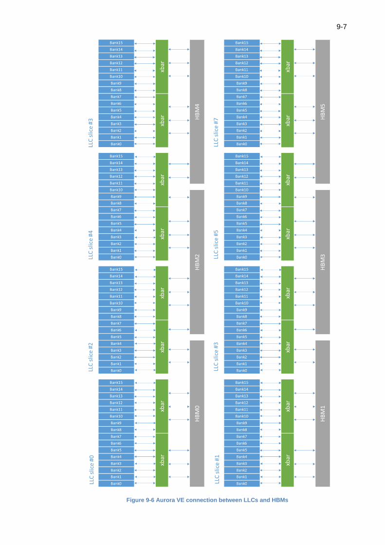
9-7
Figure 9-6 Aurora VE connection between LLCs and HBMs
9-8
9.4. NoC
The SX-Aurora TSUBASA VE has NoC (Network on Chip) to connect 8 cores and
LLC slices. It is formed as a 2D mesh shown in the Figure. The bidirectional bandwidth
per link is 819.2GB/s.
9.5. Ring bus
The SX-Aurora TSUBASA VE has a ring styled bus connecting LLC slices and DMU.
This ring bus is used for LHM/SHM data transfer, PIO access and for direct memory
access data transfer.
9.6. MCU and VE memory
For the main memory of the VE, the MCU supports 1.6Gbps HBM2 memory. The
SX-Aurora TSUBASA VE supports HBM2 memory of 4 or 8 level stacking memory
(referred to as 4-hi and 8-hi respectively). With the 4-hi HBM2 memory x 6 configuration
VE's total memory will be 24GB in size, while 48GB with the 8-hi HBM memory x 6
configuration. And VE's maximum memory bandwidth reaches 1.2TB/s with 8-hi HBM
memory.
9-9
9.7. DMU
The DMU controls the direct memory access between the VE and other external PCIe
devices or the VE host using Aurora VE's PCIe interface. It reads/writes data from/to
HBM through LLCs, therefore the consistency amongst core accesses and DMA is safely
kept (L1-I is outside of this scope). Internally The SX-Aurora TSUBASA has four DMA
engines and can operate four DMA transaction in parallel.
The DMU contains DMAATB, which controls address conversion of a VE host virtual
address to a PCIe physical address as a VH system absolute address, VE memory
absolute address or VE communication register absolute address space. It also contains
DMAATB tables and DMAATB directory. See Chapter 6 and 9 for details.
9.8. DGU
The DGU has a diagnosis/error reporting feature to keep the whole VE safe to use.
When any serious error is reported from a unit, it attempts to stop the circuit and raise
MSI-X styled interrupt(s) to the VE host, so that the VE driver component on the VE host
fetches the interrupt and then starts an error handling procedure.
9.9. PEU
The PEU is a PCI express controller that supports PCI express generation 1, 2 and 3
x 16 lanes. PEU also works as an interface block to convert protocols between PCI
express and AMBA AXI4 interface.
9.10. XIU
The XIU is a bridging unit amongst PEU, DGU and DMU. It also operates AMBA AXI4
formatted messages and translates them into hardware protocol packets, and vice versa.
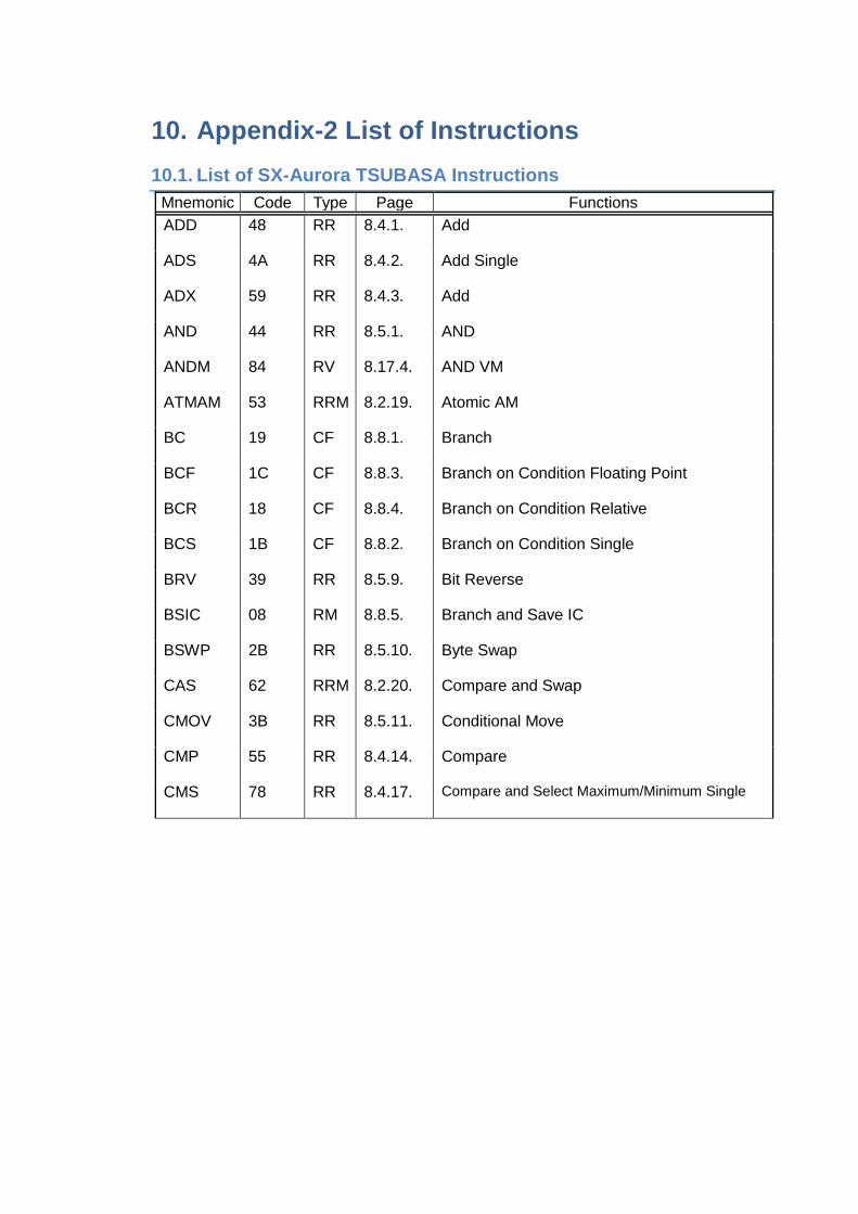
10. Appendix-2 List of Instructions
10.1. List of SX-Aurora TSUBASA Instructions
Mnemonic Code Type Page Functions
ADD 48 RR 8.4.1. Add
ADS 4A RR 8.4.2. Add Single
ADX 59 RR 8.4.3. Add
AND 44 RR 8.5.1. AND
ANDM 84 RV 8.17.4. AND VM
ATMAM 53 RRM 8.2.19. Atomic AM
BC 19 CF 8.8.1. Branch
BCF 1C CF 8.8.3. Branch on Condition Floating Point
BCR 18 CF 8.8.4. Branch on Condition Relative
BCS 1B CF 8.8.2. Branch on Condition Single
BRV 39 RR 8.5.9. Bit Reverse
BSIC 08 RM 8.8.5. Branch and Save IC
BSWP 2B RR 8.5.10. Byte Swap
CAS 62 RRM 8.2.20. Compare and Swap
CMOV 3B RR 8.5.11. Conditional Move
CMP 55 RR 8.4.14. Compare
CMS 78 RR 8.4.17. Compare and Select Maximum/Minimum Single
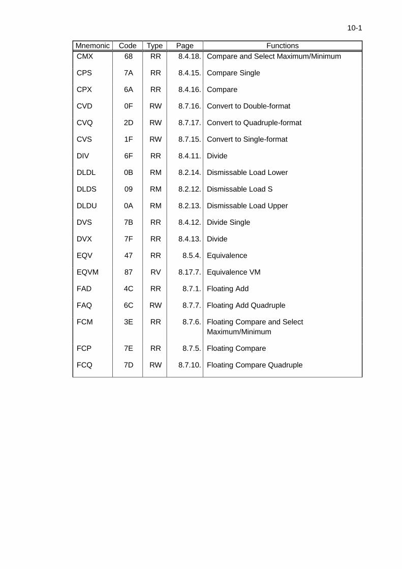
10-1
Mnemonic Code Type Page Functions
CMX 68 RR 8.4.18. Compare and Select Maximum/Minimum
CPS 7A RR 8.4.15. Compare Single
CPX 6A RR 8.4.16. Compare
CVD 0F RW 8.7.16. Convert to Double-format
CVQ 2D RW 8.7.17. Convert to Quadruple-format
CVS 1F RW 8.7.15. Convert to Single-format
DIV 6F RR 8.4.11. Divide
DLDL 0B RM 8.2.14. Dismissable Load Lower
DLDS 09 RM 8.2.12. Dismissable Load S
DLDU 0A RM 8.2.13. Dismissable Load Upper
DVS 7B RR 8.4.12. Divide Single
DVX 7F RR 8.4.13. Divide
EQV 47 RR 8.5.4. Equivalence
EQVM 87 RV 8.17.7. Equivalence VM
FAD 4C RR 8.7.1. Floating Add
FAQ 6C RW 8.7.7. Floating Add Quadruple
FCM 3E RR 8.7.6. Floating Compare and Select
Maximum/Minimum
FCP 7E RR 8.7.5. Floating Compare
FCQ 7D RW 8.7.10. Floating Compare Quadruple
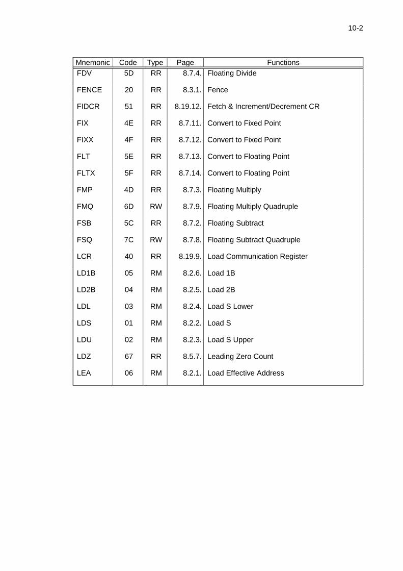
10-2
Mnemonic Code Type Page Functions
FDV 5D RR 8.7.4. Floating Divide
FENCE 20 RR 8.3.1. Fence
FIDCR 51 RR 8.19.12. Fetch & Increment/Decrement CR
FIX 4E RR 8.7.11. Convert to Fixed Point
FIXX 4F RR 8.7.12. Convert to Fixed Point
FLT 5E RR 8.7.13. Convert to Floating Point
FLTX 5F RR 8.7.14. Convert to Floating Point
FMP 4D RR 8.7.3. Floating Multiply
FMQ 6D RW 8.7.9. Floating Multiply Quadruple
FSB 5C RR 8.7.2. Floating Subtract
FSQ 7C RW 8.7.8. Floating Subtract Quadruple
LCR 40 RR 8.19.9. Load Communication Register
LD1B 05 RM 8.2.6. Load 1B
LD2B 04 RM 8.2.5. Load 2B
LDL 03 RM 8.2.4. Load S Lower
LDS 01 RM 8.2.2. Load S
LDU 02 RM 8.2.3. Load S Upper
LDZ 67 RR 8.5.7. Leading Zero Count
LEA 06 RM 8.2.1. Load Effective Address
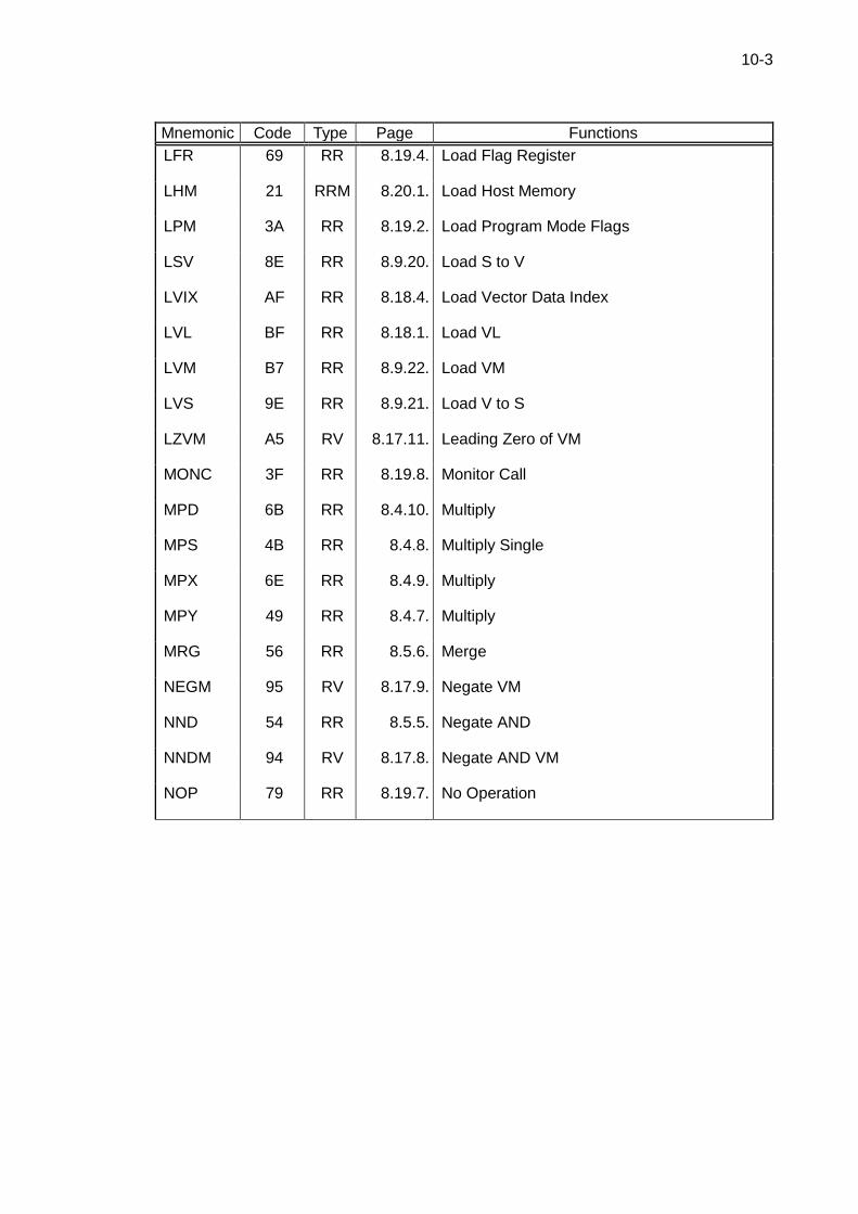
10-3
Mnemonic Code Type Page Functions
LFR 69 RR 8.19.4. Load Flag Register
LHM 21 RRM 8.20.1. Load Host Memory
LPM 3A RR 8.19.2. Load Program Mode Flags
LSV 8E RR 8.9.20. Load S to V
LVIX AF RR 8.18.4. Load Vector Data Index
LVL BF RR 8.18.1. Load VL
LVM B7 RR 8.9.22. Load VM
LVS 9E RR 8.9.21. Load V to S
LZVM A5 RV 8.17.11. Leading Zero of VM
MONC 3F RR 8.19.8. Monitor Call
MPD 6B RR 8.4.10. Multiply
MPS 4B RR 8.4.8. Multiply Single
MPX 6E RR 8.4.9. Multiply
MPY 49 RR 8.4.7. Multiply
MRG 56 RR 8.5.6. Merge
NEGM 95 RV 8.17.9. Negate VM
NND 54 RR 8.5.5. Negate AND
NNDM 94 RV 8.17.8. Negate AND VM
NOP 79 RR 8.19.7. No Operation
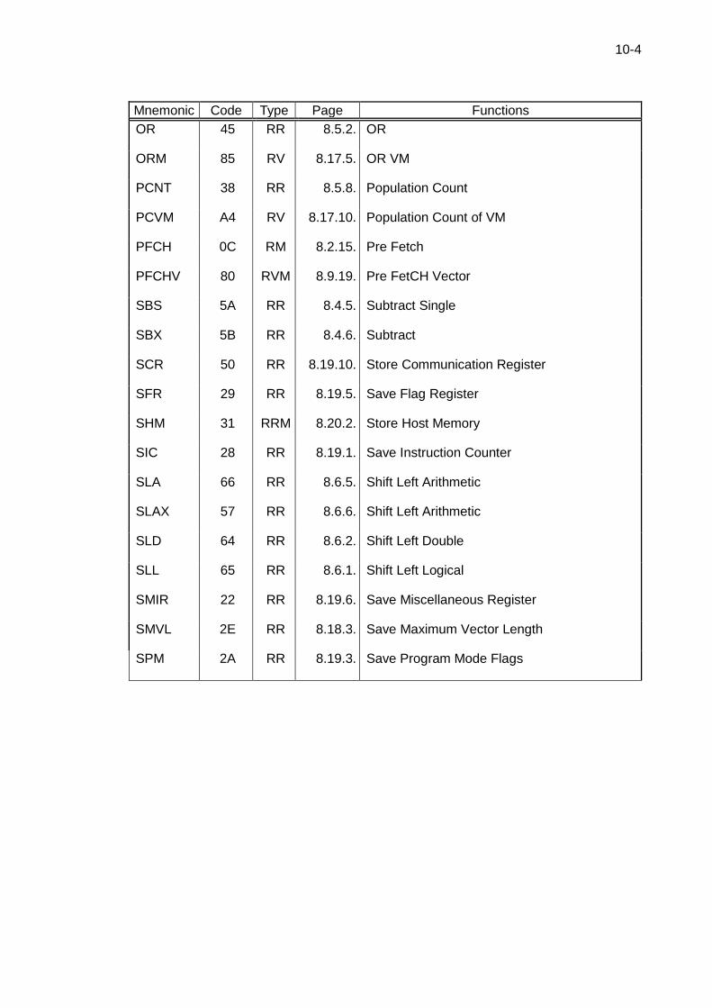
10-4
Mnemonic Code Type Page Functions
OR 45 RR 8.5.2. OR
ORM 85 RV 8.17.5. OR VM
PCNT 38 RR 8.5.8. Population Count
PCVM A4 RV 8.17.10. Population Count of VM
PFCH 0C RM 8.2.15. Pre Fetch
PFCHV 80 RVM 8.9.19. Pre FetCH Vector
SBS 5A RR 8.4.5. Subtract Single
SBX 5B RR 8.4.6. Subtract
SCR 50 RR 8.19.10. Store Communication Register
SFR 29 RR 8.19.5. Save Flag Register
SHM 31 RRM 8.20.2. Store Host Memory
SIC 28 RR 8.19.1. Save Instruction Counter
SLA 66 RR 8.6.5. Shift Left Arithmetic
SLAX 57 RR 8.6.6. Shift Left Arithmetic
SLD 64 RR 8.6.2. Shift Left Double
SLL 65 RR 8.6.1. Shift Left Logical
SMIR 22 RR 8.19.6. Save Miscellaneous Register
SMVL 2E RR 8.18.3. Save Maximum Vector Length
SPM 2A RR 8.19.3. Save Program Mode Flags
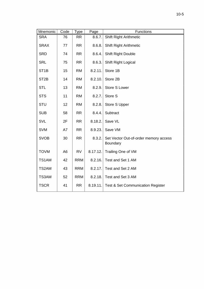
10-5
Mnemonic Code Type Page Functions
SRA 76 RR 8.6.7. Shift Right Arithmetic
SRAX 77 RR 8.6.8. Shift Right Arithmetic
SRD 74 RR 8.6.4. Shift Right Double
SRL 75 RR 8.6.3. Shift Right Logical
ST1B 15 RM 8.2.11. Store 1B
ST2B 14 RM 8.2.10. Store 2B
STL 13 RM 8.2.9. Store S Lower
STS 11 RM 8.2.7. Store S
STU 12 RM 8.2.8. Store S Upper
SUB 58 RR 8.4.4. Subtract
SVL 2F RR 8.18.2. Save VL
SVM A7 RR 8.9.23. Save VM
SVOB 30 RR 8.3.2. Set Vector Out-of-order memory access
Boundary
TOVM A6 RV 8.17.12. Trailing One of VM
TS1AM 42 RRM 8.2.16. Test and Set 1 AM
TS2AM 43 RRM 8.2.17. Test and Set 2 AM
TS3AM 52 RRM 8.2.18. Test and Set 3 AM
TSCR 41 RR 8.19.11. Test & Set Communication Register
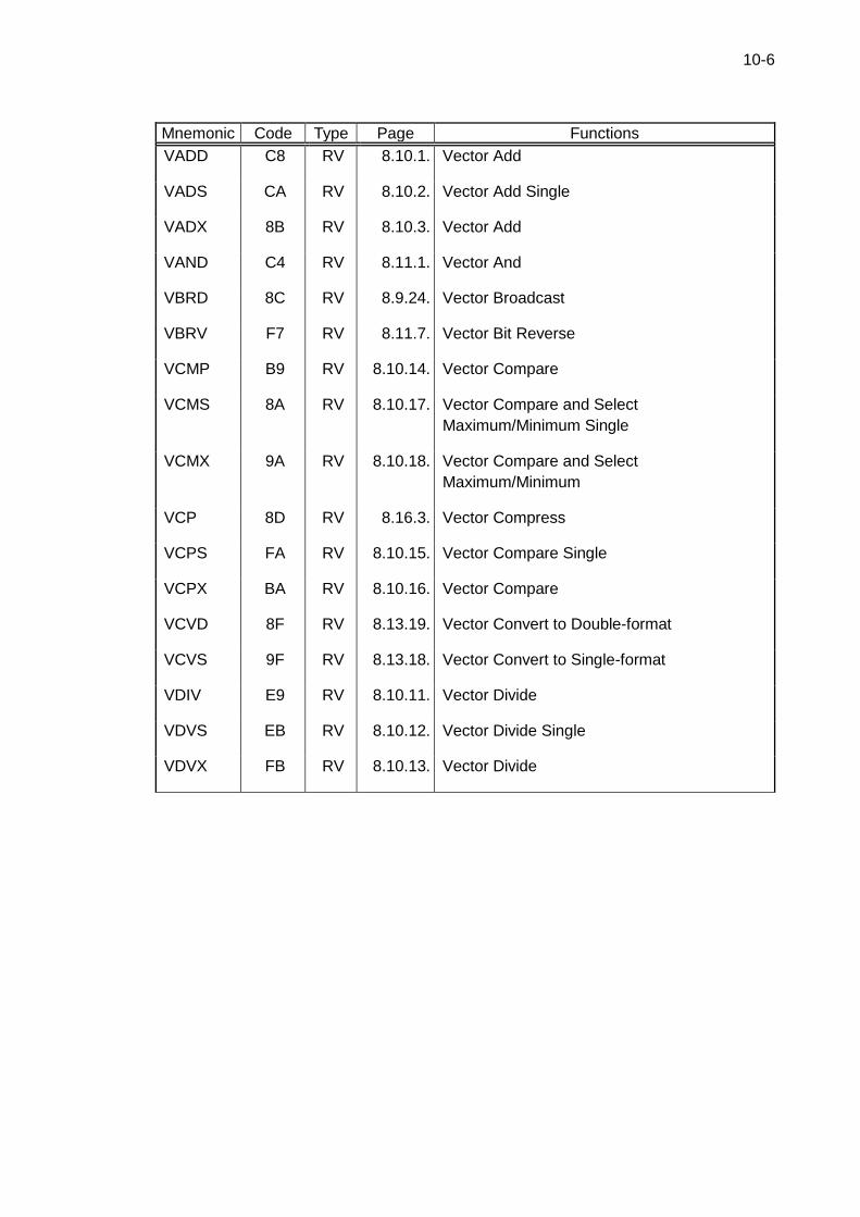
10-6
Mnemonic Code Type Page Functions
VADD C8 RV 8.10.1. Vector Add
VADS CA RV 8.10.2. Vector Add Single
VADX 8B RV 8.10.3. Vector Add
VAND C4 RV 8.11.1. Vector And
VBRD 8C RV 8.9.24. Vector Broadcast
VBRV F7 RV 8.11.7. Vector Bit Reverse
VCMP B9 RV 8.10.14. Vector Compare
VCMS 8A RV 8.10.17. Vector Compare and Select
Maximum/Minimum Single
VCMX 9A RV 8.10.18. Vector Compare and Select
Maximum/Minimum
VCP 8D RV 8.16.3. Vector Compress
VCPS FA RV 8.10.15. Vector Compare Single
VCPX BA RV 8.10.16. Vector Compare
VCVD 8F RV 8.13.19. Vector Convert to Double-format
VCVS 9F RV 8.13.18. Vector Convert to Single-format
VDIV E9 RV 8.10.11. Vector Divide
VDVS EB RV 8.10.12. Vector Divide Single
VDVX FB RV 8.10.13. Vector Divide
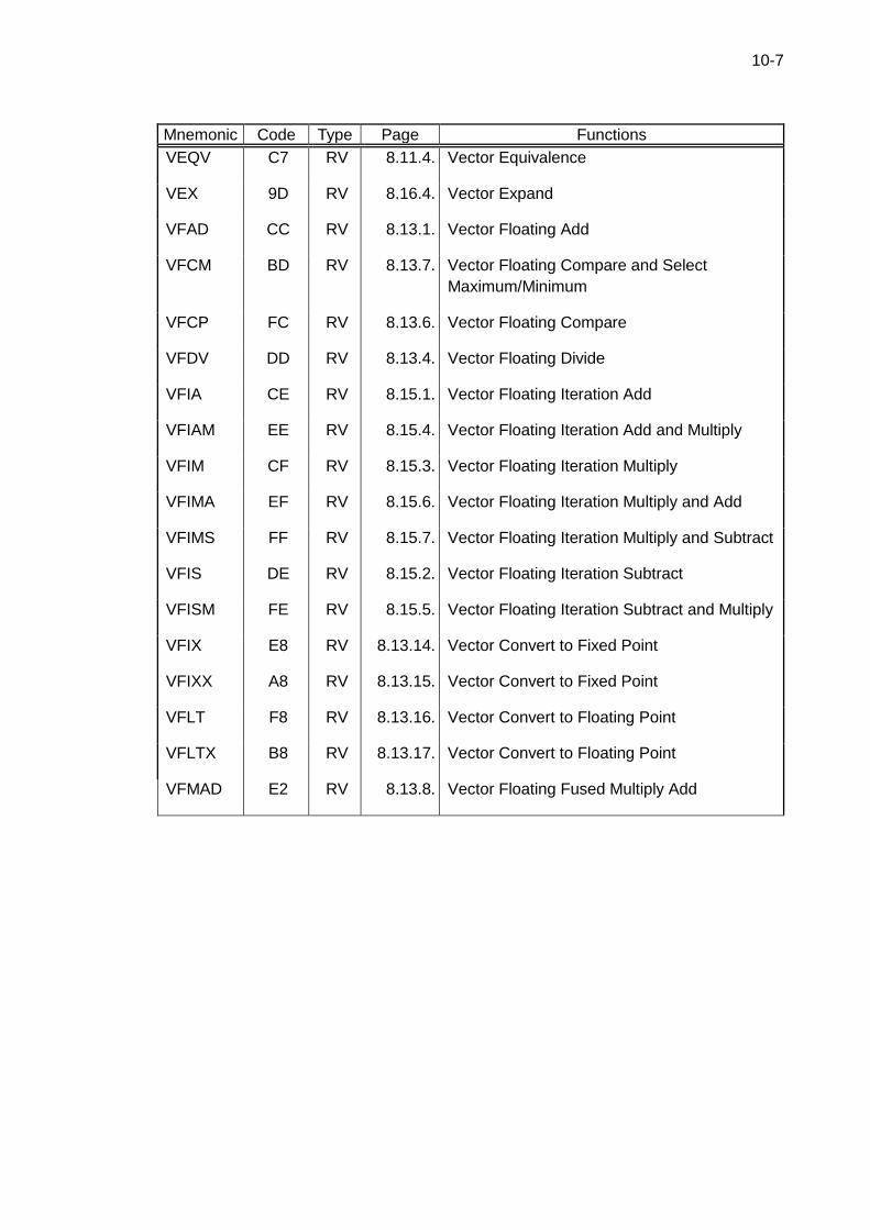
10-7
Mnemonic Code Type Page Functions
VEQV C7 RV 8.11.4. Vector Equivalence
VEX 9D RV 8.16.4. Vector Expand
VFAD CC RV 8.13.1. Vector Floating Add
VFCM BD RV 8.13.7. Vector Floating Compare and Select
Maximum/Minimum
VFCP FC RV 8.13.6. Vector Floating Compare
VFDV DD RV 8.13.4. Vector Floating Divide
VFIA CE RV 8.15.1. Vector Floating Iteration Add
VFIAM EE RV 8.15.4. Vector Floating Iteration Add and Multiply
VFIM CF RV 8.15.3. Vector Floating Iteration Multiply
VFIMA EF RV 8.15.6. Vector Floating Iteration Multiply and Add
VFIMS FF RV 8.15.7. Vector Floating Iteration Multiply and Subtract
VFIS DE RV 8.15.2. Vector Floating Iteration Subtract
VFISM FE RV 8.15.5. Vector Floating Iteration Subtract and Multiply
VFIX E8 RV 8.13.14. Vector Convert to Fixed Point
VFIXX A8 RV 8.13.15. Vector Convert to Fixed Point
VFLT F8 RV 8.13.16. Vector Convert to Floating Point
VFLTX B8 RV 8.13.17. Vector Convert to Floating Point
VFMAD E2 RV 8.13.8. Vector Floating Fused Multiply Add
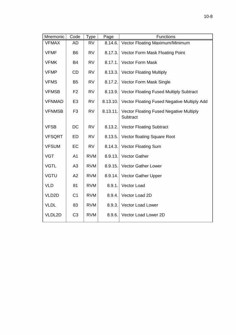
10-8
Mnemonic Code Type Page Functions
VFMAX AD RV 8.14.6. Vector Floating Maximum/Minimum
VFMF B6 RV 8.17.3. Vector Form Mask Floating Point
VFMK B4 RV 8.17.1. Vector Form Mask
VFMP CD RV 8.13.3. Vector Floating Multiply
VFMS B5 RV 8.17.2. Vector Form Mask Single
VFMSB F2 RV 8.13.9. Vector Floating Fused Multiply Subtract
VFNMAD E3 RV 8.13.10. Vector Floating Fused Negative Multiply Add
VFNMSB F3 RV 8.13.11. Vector Floating Fused Negative Multiply
Subtract
VFSB DC RV 8.13.2. Vector Floating Subtract
VFSQRT ED RV 8.13.5. Vector floating Square Root
VFSUM EC RV 8.14.3. Vector Floating Sum
VGT A1 RVM 8.9.13. Vector Gather
VGTL A3 RVM 8.9.15. Vector Gather Lower
VGTU A2 RVM 8.9.14. Vector Gather Upper
VLD 81 RVM 8.9.1. Vector Load
VLD2D C1 RVM 8.9.4. Vector Load 2D
VLDL 83 RVM 8.9.3. Vector Load Lower
VLDL2D C3 RVM 8.9.6. Vector Load Lower 2D
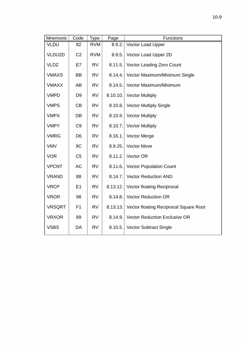
10-9
Mnemonic Code Type Page Functions
VLDU 82 RVM 8.9.2. Vector Load Upper
VLDU2D C2 RVM 8.9.5. Vector Load Upper 2D
VLDZ E7 RV 8.11.5. Vector Leading Zero Count
VMAXS BB RV 8.14.4. Vector Maximum/Minimum Single
VMAXX AB RV 8.14.5. Vector Maximum/Minimum
VMPD D9 RV 8.10.10. Vector Multiply
VMPS CB RV 8.10.8. Vector Multiply Single
VMPX DB RV 8.10.9. Vector Multiply
VMPY C9 RV 8.10.7. Vector Multiply
VMRG D6 RV 8.16.1. Vector Merge
VMV 9C RV 8.9.25. Vector Move
VOR C5 RV 8.11.2. Vector OR
VPCNT AC RV 8.11.6. Vector Population Count
VRAND 88 RV 8.14.7. Vector Reduction AND
VRCP E1 RV 8.13.12. Vector floating Reciprocal
VROR 98 RV 8.14.8. Vector Reduction OR
VRSQRT F1 RV 8.13.13. Vector floating Reciprocal Square Root
VRXOR 89 RV 8.14.9. Vector Reduction Exclusive OR
VSBS DA RV 8.10.5. Vector Subtract Single
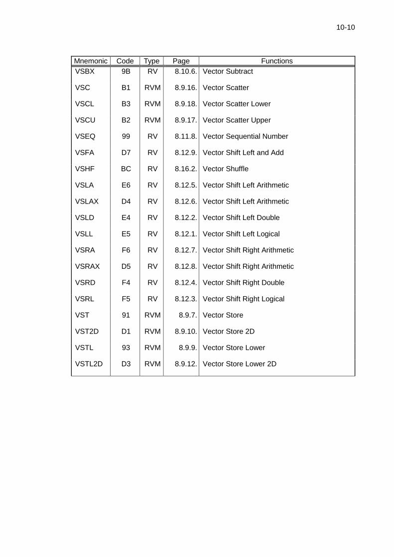
10-10
Mnemonic Code Type Page Functions
VSBX 9B RV 8.10.6. Vector Subtract
VSC B1 RVM 8.9.16. Vector Scatter
VSCL B3 RVM 8.9.18. Vector Scatter Lower
VSCU B2 RVM 8.9.17. Vector Scatter Upper
VSEQ 99 RV 8.11.8. Vector Sequential Number
VSFA D7 RV 8.12.9. Vector Shift Left and Add
VSHF BC RV 8.16.2. Vector Shuffle
VSLA E6 RV 8.12.5. Vector Shift Left Arithmetic
VSLAX D4 RV 8.12.6. Vector Shift Left Arithmetic
VSLD E4 RV 8.12.2. Vector Shift Left Double
VSLL E5 RV 8.12.1. Vector Shift Left Logical
VSRA F6 RV 8.12.7. Vector Shift Right Arithmetic
VSRAX D5 RV 8.12.8. Vector Shift Right Arithmetic
VSRD F4 RV 8.12.4. Vector Shift Right Double
VSRL F5 RV 8.12.3. Vector Shift Right Logical
VST 91 RVM 8.9.7. Vector Store
VST2D D1 RVM 8.9.10. Vector Store 2D
VSTL 93 RVM 8.9.9. Vector Store Lower
VSTL2D D3 RVM 8.9.12. Vector Store Lower 2D
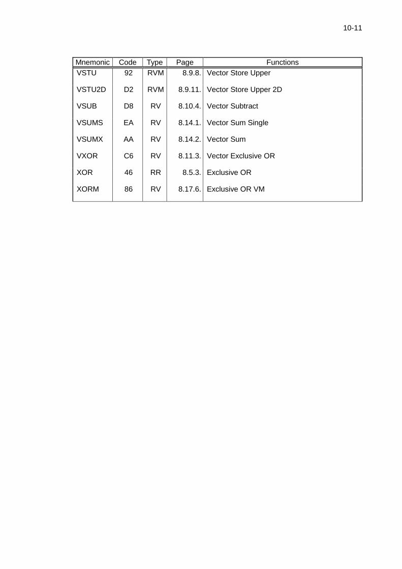
10-11
Mnemonic Code Type Page Functions
VSTU 92 RVM 8.9.8. Vector Store Upper
VSTU2D D2 RVM 8.9.11. Vector Store Upper 2D
VSUB D8 RV 8.10.4. Vector Subtract
VSUMS EA RV 8.14.1. Vector Sum Single
VSUMX AA RV 8.14.2. Vector Sum
VXOR C6 RV 8.11.3. Vector Exclusive OR
XOR 46 RR 8.5.3. Exclusive OR
XORM 86 RV 8.17.6. Exclusive OR VM
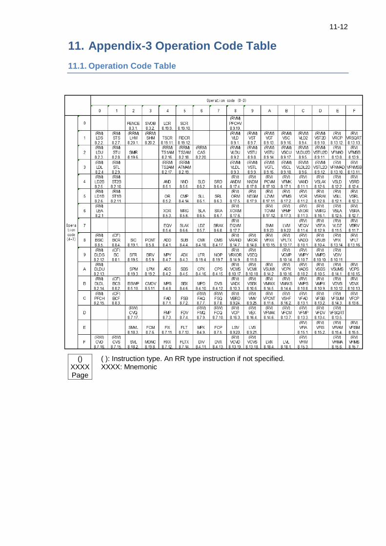
11-12
11. Appendix-3 Operation Code Table
11.1. Operation Code Table
() XXXX Page
( ): Instruction type. An RR type instruction if not specified. XXXX: Mnemonic

11-13