Embed Size (px)
Citation preview

Power Supply Design Seminar
Topic Categories:Basic Switching TechnologySpecific Power Topologies
Reproduced from1984 Unitrode Power Supply Design Seminar
SEM300, Topic 1TI Literature Number: SLUP067
© 1984 Unitrode Corporation© 2011 Texas Instruments Incorporated
Power Seminar topics and online power- training modules are available at:
power.ti.com/seminars
Switching Power Supply Topology Review

TexasInstruments 1 SLUP067
Switching Power Supply Topology ReviewLloyd H. Dixon, Jr.
This paper reviews the characteristics of the three basic circuit families commonly used in switching regulated power supplies: buck, boost and flyback (or buck-boost). These three circuit topologies may be operated in one of two modes: the discontinuous or continuous inductor current modes. The choice of operational mode has great effect on the overall characteristics. The control method used can also help to minimize the problems associated with any topology and operational mode. Three control methods that operate at fi xed frequency are exami ned: di rect duty cycl e control, voltage feedforward, and current mode (two-loop) control. Several extensions of the basic circuits are also discussed, with the relative merits of each topology--operational mode--control method combination.
THREE BASIC TOPOLOGIES:
The three basic configurations shown in Figure 1 are: Buck, Boost and Flyback. The Cuk converter, which is not discussed, is an inversion of the flyback topology. The three different switching circuits employ the same three elements: inductor, transistor and diode, but arranged in a different manner (the output capacitors are filter elements, not part of the switching circuits). Theoretically, there are three other circuits possible using the same three elements with T configuration, but these are simply mirror images of the fi rst three and coupl e power in the opposi te di recti on.
~f] BUCK
BOOST
One common principle that applies to Figure 1. all three topologies, regardless of operational mode or control method is: In steady state operation, the vol tage across the inductor, averaged over each switching cycle, must equal zero. Otherwise, the average inductor current would change, violating the steady state premise.

TexasInstruments 2 SLUP067
Each of the three basic circuit families has a unique set of relationships between input and output voltages, currents, and duty cycle. For example, the basic buck regulator functions only with output vol tage, Vo , less than Vin and with the same polarity. The basic boost circuit requires Vo greater than Vin with the same polarity. The f1yback topology functions with Vo either greater or less than Vin, but the polarity must be opposite.
DISCONTINUOUS MODE OPERATION:
In the discontinuous inductor current mode, or "discontinuous mode", buck, boost and flyback circuits behave in a similar way. The inductor current is zero (hence discontinuous) during the last part of each switching cycle. During the first part of the cycle, the inductor current increases from zero, storing energy taken from the input. During the second part, all of this stored energy is discharged into the load, pumping energy from input to output.
Current Waveforms. Discontinuous mode current waveforms are shown in Figure 2. The inductor, transistor and diode waveforms are the same regardless of circuit topology, but the input and output current waveforms differ for each circuit according to which of the three elements are in series with the input and the output.
Three S ta tes. The re are th ree distinct operational states during each switching cycle:
1. During the transistor "on" time, ton, inductor current IL rises from zero to the peak value i p• This peak current equates to energy stored in the inductor, LI2/2, at the end of ton. During this time the inductor current is drawn from the input, and this energy stored in the inductor each cycle is power taken from the input source.
2. When the transistor turns off, the inductor voltage reverses and its stored energy forces the same peak current to flow through the diode. During the diode conduction time, td, the inductor current drives the output and linearly decreases to zero. At the end of td, all the energy that was stored in the inductor has been delivered to the output.
3. When the current reaches zero, the inductor has no more energy. The current in all switching circuit elements is zero for the remainder of the switching period. During
1--
lin: 10:
T
Buck Boost Flyback
IQ IL IQ
IL Id Id
Fi gure 2.

TexasInstruments 3 SLUP067
this idle time, tiP the circuit waits for the next clock pulse to turn the transistor back on and begin the next cycle.
Discontinuous Mode Boundary. When load current increases, the control circuit causes transistor ton (duty cycle) to increase. Peak inductor current then becomes greater and diode conduction time td must also increase. Consequently, an increase in load current causes a steady state reduction in the idl e time, ti' When load current increases to a certain level, ti becomes zero, and the discontinuous mode boundary is reached. If the load current is further increased, the inductor current will no longer discharge to zero every CYCle, and continuous mode operation results. The circuit will become unstable because the loop gain compensati on requi red for stabl e di scontinuous mode operation is not adequate to prevent oscillation in the continuous mode. It is imperative for the control circuit to sense and limit the inductor current to prevent crossing this mode boundary.
Excellent Closed Loop Response. In the di scontinuous mode, it is easy to obtain excellent response in correcting disturbances that result from large step changes in line voltage and load current, because the inductor alway starts each switching cycle with zero stored energy. This makes it possible for the control circuit to obtain any energy level (and power output) required, from zero to full output, on a cyel e-by-cycl e basis. The inductor "vanishes" from the small signal closed loop characteristic, leaving only the output capacitor with its 90 degree phase lag. The resulting Single-pole characteristic is inherently stable and easy to deal with in closing the loop (see the separate paper on "ClOSing the Feedback Loop"). The right-half-plane (RHP) zero which severely limits closed loop response in continuous mode boost and flyback circuits is not present in the discontinuous mode topologies.
High Peak Current. The one main disadvantage of the discontinuous mode is the high peak current through the tranSistor, diode and output fit tel" capaci tor. Thi s requi res semi conductors wi th hi gher current capability and puts an extreme burden on the output filter capacitor ESR (equivalent series resistance) and RMS current rating requirements. For example, in both boost and flyback cirCUits, the diode is in the output, and therefore the average diode current, Id, must equal the DC output current, 10 , Under full load conditions, if diode time td is 50% of the switching period, the peak current is 4 times the full load 10 ,
In the buck circuit the inductor current with its better form factor drives the output, so the peak current is somewhat less in proportion to the output current. However, the buck topology is seldom used in the discontinuous mode because the continuous mode provides much better performance.
Poor Open Loop Line and Load Regulation. The basic DC equation for the flyback topology operated in discontinuous mode is given below. The boost regulator has a similar but more complex formula (see "Closing the Feedback LoOpll). For the f1yback circuit:
1

TexasInstruments 4 SLUP067
It can be seen from this equation that if the duty cycle is fixed (open control loop), Va varies directly with Vin and the square root of the output load reSistance, Ro. In other words, the open loop line and load regulation is quite poor, and duty cycle D must be changed considerably by the control circuit to maintain the desired output voltage under the full range of line and load conditions.
Control Method. In all th ree constant frequency contra I methods [direct duty cycle, voltage feedforward, and current model, the output voltage is compared with a fixed reference voltage. The resulting error voltage is amplified and used as the closed loop control voltage, Vc.
Direct Duty Cycle Control: Transistor duty cycle 0 = ton/T is varied in proportion to control voltage VC' Poor open loop line and load regulation requires fairly high loop gain for correction. The output filter capacitor is part of the closed loop system and introduces a phase lag which delays correction of Vin changes.
Voltage Feedforward Control: A sample of the input voltage is fed directly into the control circuit and causes the duty cycle to vary inversely with Vin as well as directly with Vc [0 = KVc/Vin}' If Vin increases, 0 decreases automatically so that the input volt-seconds (VinO) remains constant for a fixed Vc. Thus, Vc controls input volt-seconds directly. Open loop line regulation is good, so that less closed loop gain is required to meet DC regula~on requirements. Equa~on 1 becomes:
(2)
where K is the feedforward ratio = VinO/Vc'
Current Mode Control: An inner, Second control loop compares the peak inductor current, Ip, to the control voltage, VC' In the outer loop, Vc now controls Ip directly. The inner loop provides good inherent line regulation, similar to voltage feedforward. Equation 1 becomes:
(3)
where K is the inner loop current control factor = maxIp/maxVc •
Either voltage feedforward or current mode control is recommended. They both have essentially the same good effect -- improved open loop line regulation, providing instantaneous correction to line changes and requi ri ng less closed loop gai n.
CONTINUOUS MODE OPERATION
In the continuous inductor current mode (continuous model, the inductor current is never zero during any part of the switching cycle (see Figure 3). Compared to the discontinuous mode for the same application parameters, the continuous mode requires much greater inductance. The inductor ripple current is small compared to the full load output current.

TexasInstruments 5 SLUP067
Current Waveforms. Continuous mode waveforms are shown in Figure 3. Just as with the discontinuous mode, the inductor, transistor and diode current waveforms are exactly the same for the buck, boost 0 r fl yback circuits, but the input and output waveforms differ according to which of the three elements are in series wi th input and output.
The boost and fl yback ci rcui ts have similar behavior. In both cases, the output current is the diode current, Id, which is discontinuous. The peak output current is slightly more than half the value encountered in the discontinuous mode. This reduces the burden on the output capacitor.
The buck regulator behaves very differently. Its output current is the inductor current, which is not di sconti nuous, but has a rei ative I y gentle slope and small ripple
r--- T
Buck Boost
Figure 3.
[ -I
Flyback
III Id
amplitude. This waveform is easy to filter, substantially reducing the output capacitor ESR and current rating requirements. For this reason, the continuous mode buck regulator is the most popular switching power supply configuration, particularly at higher power levels where the much higher peak current encountered with all other configurations put an intolerable burden on the output fit te r capaci to r.
Two States, Because the inductor current is never zero, there is no idle time in the continuous mode and only two operational states during each switching cycle.
1. During transistor "on" time, ton, inductor current IL increases from an initial value (greater than zero) to a higher value, replacing the inductor energy given up during the "off" time. Current (and power) is drawn from the input.
2. When the transistor is off, the diode conducts for the rest of each cycle. IL declines to the initial value, never reaching zero but giving up energy to the output.
In continuous mode operation, the upslope and downslope of inductor current are dependent only upon the input and output voltage levels and totally independent of the average inductor current or output load current. Without the flexibility provided by the third (idle) state of the discontinuous mode, Vin, Vo and duty cycle D are related differently for each topology. In the buck regulator, for example, the average voltage at the input side of the inductor is Vinton/T, or VinD, while the voltage at the inductor output is Vo. In the steady state, the average voltage

TexasInstruments 6 SLUP067
across the inductor must be zero, so Vo = VinD. This is the basic DC equation for the buck regulator. There are no terms relating to load current or resistance, which indicates excellent open loop load regulation. When Io changes, steady-state IL also changes, but the inductor ripple current and Vo do not change.
Continuous Mode Boundary -- Minimum Load Current. When the load current decreases, the duty cycle and inductor ripple current do not change (except momenta ri I y), but the average inductor current declines proportionately. For the buck regulator Io = IL, for boost and flyback Io = (1-DlIL. At a certain critical load current level, the inductor current reaches zero at the minimum of the ripple waveform. This is the boundary for continuous mode operation. If the load current further decreases, the third state idle time appears, and the circuit operates discontinuously, with completely different operating characteristics. DC regulation degrades radically. In a continuous mode regulator, the load current must not be allowed to drop below the critical level where this boundary is crossed. This minimum load requirement is a disadvantage of continuous mode systems.
Poor Closed Looo Resoonse. Small signal response of continuous mode regulators is much worse than discontinuous mode circuits because of the two pole second order characteristic of the resonant LC filter. Boost and flyback circuits also have a righthalf-plane zero in their loop gain characteristic. While it is theoretically possible to compensate for the two filter poles, the capacitors used in the compensation network charge to unusual voltage levels during periods of large signal limited operation, when inductor current cannot keep up with changes in load current. This causes output voltage offset errors which take considerable time for correction (see separate paper: "Closing the Feedback Loop"). Current mode control overcomes this problem in continuous mode buck regulators by eliminating the inductor pole. Only the single first order filter capacitor pole remains, the same as in th e di sconti nuous mode ci rcuits.
The RHP zero associated with boost and flyback continuous mode circuits is much more difficult to deal with. In buck regulators, output current Io equals inductor current IL, but in boost and flyback circuits, Io = IL(1-D). Consider the process in a f1yback regulator. When load current increases, the output capacitor voltage immediately starts to drop. The resulting error voltage temporarily increases the duty cycle, 0, causing the inductor current to rise to accommodate the increased load. However, it may take many cycles for the inductor current to complete its rise. During this time, increased 0 makes (1-0) smaller, so the output current is temporarily decreased, the opposite of what is desired. This additional lag because of the RHP zero inevitably forces the loop gain crossover frequency to be much lower than otherwise desired.
There is in addition a large signal problem with continuous mode circuits--the inability to rapidly slew the inductor current as desired with large step changes in load. This is because of the I a rge i nducto r va I ues used in conti nuous mode ci rcui ts. The

TexasInstruments 7 SLUP067
problem is most severe when attempting to increase the inductor current when operating near minimum Vin, especially if the circuit has been designed with input volt-second capability, VinD, only sl ightly greater than requi red for steady state operation.
Good Open Loop Load Regulation, Poor Line Regulatign. The basic DC equations for the continuous mode are:
Buck: Boost: Flyback: [4) Vo :: VinD Vo = Vin/ [1-D) Vo :: VinD/[1-D)
Unlike the discontinuous mode, tha above equations reveal that the DC output voltage, Va' is totally independent of output current or reSistance, depending only upon Vin and D. The duty cycle does not change with steady-state changes in load current, but D must be changed to make correction for changes in Vine
Direct Duty Cycle Control. Moderately high loop gain is required to correct the inherent poor open loop line regulation. It is difficul t to design the closed loop, and many problems cannot be overcome. See earlier comments under "Poor Closed Loop Response. 1I
Voltage Feedforward. Voltage feedforward applied in the same way as the discontinuous mode topologies provides good open loop line regulation in the continuous mode buck regUlator. Equation 4 (buck) becomes:
(5)
Open loop line and load regulation are both good. Closed loop gain is now required only for good dynamiC response to changes in load. Boost and flyback topologies in the continuous mode are only partially compensated by this simple feedforward technique. Methods that are more complex will achieve compensation, but they are beyond the scope of this paper.£1)
Current Mode Control. Applied to continuous mode buck regulators, current mode control provides greatly improved performance. First, the inner current control loop provides inherent good line regulation, even with the outer loop open. Second, the inner loop eliminates the filter inductor pole so that the outer loop no longer has a two-pole second order resonant characteristic, but only the Single filter capaCitor pole. The gain characteristic becomes very easy to compensate. Thi I'd, compensation capaci tors at the error amplifier input [which cause output voltage errors after large signal I imi ted operation) are not requi red because the inductor pole is eliminated. Current mode control has the single disadvantage that it introduces load current dependency which does need closed loop correction. Buck regulator Equation 4 becomes:
[6 ) K = maxIL/maxVc
Current mode control also facilitates the paralleling of several individual power supply modul es. The current control loop insures that each module will always deliver its assigned proportion of the total load current.

TexasInstruments 8 SLUP067
In the continuous boost and flyback topologies, the performance improvements from current mode control are less dramatic. Only partial voltage feedforward compensation is accomplished. When Vin changes, the inner current control loop maintains IL constant, but 10 will change because the (1-0) factor relating IL to 10 in boost and f1yback ci rcui ts changes wi th Vi n'
Current mode control does eliminate the inductor pole and thereby simplifies the closed loop design, but it does not eliminate the RHP zero, which is the worst limitation of the continuous mode boost and flyback circuits.
TRANSFORMER COUPLED ADAPTATIONS OF THE BASIC TOPOLOGIES:
Transformer coupled versions of the basic circuits provide several important advantages, particularly in applications where primary power is the 120 V or 230 V AC line. First, the transformer provides the isolation required for off-line power supplies. Second, the transformer permits a turns ratio adjustment which avoids the very small duty cycle and high peak currents that would otherwise occur when input and output voltages are very different, as in most off-line applications. The ability to set the turns ratio also removes the Vin vs. Vo and polarity restrictions that apply to the basic topologies. Also, multiple outputs at various voltages are easily obtained with multiple secondary windings.
Transformer coupling introduces some new problems, however. These include: additional cost, size and weight, losses in the core and windings, potential core saturation (especially in push-pull circuits), core reset in single-ended circuits, and voltage spikes and losses due to transformer leakage reactance.
Forward Converter (Buck). single ended forward converter +~
The
i n Fig u r e 4. i sid e n tic a Ito pWM J the basi c buck regul ato r with J the addition of a transformer and series diode. The trans- - 0.------'
former provides line isolation
L
and usually a large step-down Figure 4. Forward Converter turns ratio when operated off the rectified and crudely filtered AC line. For example, with 200-400 V DC input and 5 V output, a turns ratio of 15:1 is typical, to increase the duty cycle to near 50% and reduce the peak primary current.
The steady-state vol tage across any transformer or inductor must average zero, or the current must change (which is not steadystate) and the core will saturate. In a push-pull system, this naturally occurs because of the symmetry of the al ternating positive and negative waveform applied to the windings. In a single ended forward converter, this does not happen naturally. Specific provision must be made to reset the core by allowing the voltage across the windings to backswing during the transistor "off" ti me so that the reverse vol t-seconds equal and cancel the volt-seconds applied during the "on" time.

TexasInstruments 9 SLUP067
The series diode is required to decouple the secondary and permit this vol tage backswing. To protect the transistor, the backswing must be limited by some kind of clamp. This is often accomplished by a tertiary transformer winding, bifilar with the primary, which is diode clamped to Vin (the clamp is essential, but not shown in Figure 4). With the backswing thus clamped to Vin, the backswing vol tage is the same as the forward vol tage appl ied during the nonn time. This means ton (and D) must be limited to 50%, otherwise the forward volt-seconds will exceed the reverSe volt-second capability and the transformer will saturate. In summary, (1) clamp the backswing, and (2) clamp the maximum duty cycle so the forward volt-seconds can never exceed the reverse volt-second capability. With the backswing clamped to a reverse voltage equal to the forward, the voltage applied to the transistor will be 2 times Vin.
Tr-ansformer uti I ization in the singl e-ended forward converter is not as good as in a push pull converter, because power is not transferred during the time allowed for core reset. However, the forward converter is very popular at power levels up to 1 KW because the single ended base drive circuitry costs less.
Additional secondaries are often used when multiple output voltages are required. The continuous mode is always used because of the ease of fil tering the small inductor ripple current. Current mode control is definitely advantageous.
Push-Pull Center-tap (Buck] Figure 5 shows a push-pull centertap version of the buck regulator with two outputs whose vol tages wi II
PWM IIIp
proportion according to . PWM
their respective secondary ~ turns. The push-pull drive automatically provides core reset on alternate half cycles, but these alternate half cycles must be quite symmetrical or the vol t-
Figure 5. Push-Pull Centertap
seconds will not cancel, resulting in core saturation. Symmetry can be spoiled by unequal transistor storage times or Vce[sat]. Many papers have been written on symmetry correction circuits, but the best method is to use a current mode controf IC such as the UC1846, which senses unbalance in the primary current waveform and automatically corrects by changing the pulse widths of alternate hal f cycl es.
Transistor voltage ratings must be 2 times Vin because of the doubling effect of the centertap primary. Peak reverse rectifier voltage may be 5 or 6 times Va, assuming 2:1 Vin range. Dual base drive circuits ~re ~equired.
Buck regulators are inherently "vol tage-fed", that is they are driven from a voltage source and there are only low impedance

TexasInstruments 10 SLUP067
elements in the input circuit. This creates a substantial risk of damage or destruction of the switching transformers in the event of a temporary downstream faul t condition, such as transformer saturation due to drive asymmetry, poor rectifier recovery characteristics, or transistor conduction overlap due to storage time with inadequate deadband provided by the control IC. These events, often transitory, have been responsible for many switching power supply failures, and they are hard to prove. These problems are eliminated by proper design and component selection.
In any buck regulator with multiple outputs, when unbalanced step changes in load occur, dynamic cross-regulation between outputs is extremely poor because of the dynamic isolation caused by the filter inductors in series with each output. This problem may be corrected by eliminating the individual inductors, coupling them by placing all the inductor windings on a common core. Perfect coupling should not be sought, however, because slight voltage differentials due to such things as unmatched rectifier forward drops will cause high circulating ripple currents. Design the coupled inductor to have 10-20% leakage inductance. This controls the circulating currents with little impairment of dynamic crossregulation.(2)
With any topology, to get good dynamic response with large step change from light load to full load, and during full load startup, the short ci rcuit current limit must be substantially greater than the fu II load cu rrent.
Half Bridge (Buck). The +o---__ --~ half bridge is also a push-pull version of the buck regulator. As shown in Figure 6, two series bulk fit ter capacitors provide a tapped input sou rce. The two transistors connect the
PWM
single transformer primary -o--~-~ '----' across the two capacitors alternately. The primary voltages and currents are symmetrical AC. DC current is not drawn from the center-tap
Figure 6. Half Bridge
of the input suppl y.
The bi g advantage of the ha I f b ri dge agai nst the push-pu II centertap configuration discussed previously is that the transistor voltage ratings are cut in half (although the current is doubled). This has become less important with higher voltage rating transistors more available. Base drive transformers must be used because the two base-emitters do not have common reference unless complementary NPN/PNP transistor are used, which they seldom are. The same problem with transformer drive asymmetry potentially exists.
This configuration has been extremely popular in the past. In 1983, most designers would question its cost-effectiveness at power levels under 1 KW.
TexasInstruments 11 SLUP067
Full B ri dge (Buck). The full bridge (not shown) is a higher power extension of the half bridge. the circuit is identical to Figure 6 except the two series capacitors are replaced by two more transistors identical to the first two which complete the bridge. For a given power level, the transformer primary voltage is double that of the half bridge and the current is halved. The transistor voltage ratings are the same, but there are twice as many, and the transistor currents are halved.
PWM
Single-Ended Flyback. At first glance, the circuit of Figure 7 looks much like the forward converter of Figure 4. However, the transformer in Figure 4 is not a transformer, but an inductor with primary and seconda ry wi ndi ngs. Its purpose is to store energy.
Figure 7. Single-Ended Flyback
(The purpose of a true transformer is to directly couple not to store it.) This is the shunt inductor of the topology, as in Figure 1.
energy, fl yback
The inductor primary and secondary have polarity opposite the forward converter transformer. When the transi stor is "on", primary current (and inductor energy) is increaSing, but during this time the output rectifer is reverse biased. When the transistor turns off, the inductor voltage reverses and maintains the same instantaneous ampere-turns through the secondary and the rectifier to the output, in order to maintain the energy stored in the core (or gap). Just as with the previous buck regulators, the multiple windings provide line isolation and the opportunity to adjust the turns ratio to optimize the duty cycle and minimize peak primary current.
The flyback topology is quite amenable to multiple outputs by applying additional secondari es wi ththe approp ri ate tu rns rati os. The dynamic cross-regulation between these multiple outputs is theoretically quite good, because there is no filter inductor in series with each output to spoil the dynamic coupling, as in the buck regulator ci rcuits. However, I eakage inductance between the secondaries can severely hurt the cross-regulation, and considerable care must be applied to the design of the inductor in this respect.
The single ended flyback circuit is quite popular at low power levels because of its simplicity and low cost. Its big disadvantage in the discontinuous operating mode is the high peak current in the transistor and the output which makes the filter capacitor problem quite painful. The continuous mode does not quite cut the peak current in half, but brings in other problems such as the RHP zero and difficul t compensation methods with poor transient response. In 1983, many sophisticated designers use this flyback technique up to 200-300 Watts.
TexasInstruments 12 SLUP067
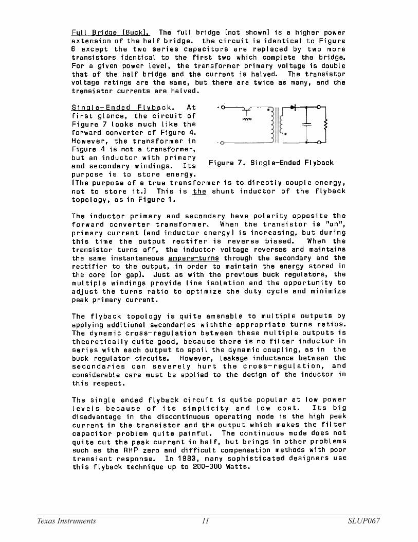
Push-Pull Boost. This last exam pi e--compare the pushpull boost regulator in Figure 8 with Figure 1. The transistors alternately apply the input inductor current to the transformer primary and the outputs. Where is the shunt transistor in the Figure 1 boost regulator that "recharges" the inductor? The two transistors in the primary
Figure 8. Push-Pull Boost
of the transformer provide this switching function by del iberatel y making them conduct simultaneously, thus shorting out the primary, when it is desired to recharge the inductor. In this method, which eliminates the need for a third, shunt transistor, the two transistors are either both on, or on individually. They are never both off, as in the push-pull buck regulators. A little innovation in the control-base drive technique is necessary.
Like the flyback, the boost regulator has no filter inductor in series with each output, so the dynamic cross-regulation is good.
All boost topologies are inherently "current-fed", because of the inductor in series with the input. Because of this, boost regulators can shrug off temporary downstream fault conditions such as core saturation, poor rectifier recovery, or transistor conduction overlap. All these things do is help recharge the inductor current. Boost converters also generate much less EMI at the input because the input current waveform has small AC content.
RECOMMENDATIONS: For post regulation, point of load regulation and for developing additional voltages from an existing line isolated DC supply (CM = Current mode, FF = Feedforward):
For step-down: Buck, Continuous, CM For step-up: For reverse polarity:
Boost, Discontinuous, FF or CM Flyback, Discontinuous, FF or CM
For applications that require transformer coupled circuits for isolation and/or multiple outputs:
Under 200 W: 200 W--1 kW: Over 1 kW:
REFERENCES:
Flyback, Discontinuous, FF or CM Forward Converter (Buck), Continuous, CM Half Bridge, Ful I Bridge, Continuous, CM
1 L. H. Dixon, Jr., "Pulse Width Modulator Control Methods with Complementary Optimization," Powerconversion International, January 1982, pp 14-21.
2. H. Matsuo and K. Harada, "New Energy Storage DC-DC Converter with Multiple Outputs," Solid State Power Conversion, Nov./Dec. 1978, pp 54-5a.

TI Worldwide Technical Support
InternetTI Semiconductor Product Information Center Home Pagesupport.ti.com
TI E2E™ Community Home Pagee2e.ti.com
Product Information CentersAmericas Phone +1(972)644-5580
Brazil Phone 0800-891-2616
Mexico Phone 0800-670-7544
Fax +1(972)927-6377 Internet/Email support.ti.com/sc/pic/americas.htm
Europe, Middle East, and AfricaPhone EuropeanFreeCall 00800-ASK-TEXAS (0080027583927) International +49(0)8161802121 RussianSupport +7(4)959810701
Note:TheEuropeanFreeCall(TollFree)numberisnotactiveinallcountries.Ifyouhavetechnicaldifficultycallingthefreecallnumber,pleaseusetheinternationalnumberabove.
Fax +(49)(0)8161802045Internet support.ti.com/sc/pic/euro.htmDirectEmail [email protected]
JapanPhone Domestic 0120-92-3326
Fax International +81-3-3344-5317 Domestic 0120-81-0036
Internet/Email International support.ti.com/sc/pic/japan.htm Domestic www.tij.co.jp/pic
AsiaPhone International +91-80-41381665 Domestic Toll-FreeNumber Note:Toll-freenumbersdonotsupport
mobileandIPphones. Australia 1-800-999-084 China 800-820-8682 HongKong 800-96-5941 India 1-800-425-7888 Indonesia 001-803-8861-1006 Korea 080-551-2804 Malaysia 1-800-80-3973 NewZealand 0800-446-934 Philippines 1-800-765-7404 Singapore 800-886-1028 Taiwan 0800-006800 Thailand 001-800-886-0010Fax +8621-23073686Email [email protected]@ti.comInternet support.ti.com/sc/pic/asia.htm
A122010
Important Notice:TheproductsandservicesofTexasInstrumentsIncorporatedanditssubsidiariesdescribedhereinaresoldsubjecttoTI’sstandardtermsandconditionsofsale.CustomersareadvisedtoobtainthemostcurrentandcompleteinformationaboutTIproductsandservicesbeforeplacingorders.TIassumesnoliabilityforapplicationsassistance,customer’sapplicationsorproductdesigns,softwareperformance,orinfringementofpatents.Thepublicationofinformationregardinganyothercompany’sproductsorservicesdoesnotconstituteTI’sapproval,warrantyorendorsementthereof.
E2EandUnitrodearetrademarksofTexasInstruments.Allothertrademarksarethepropertyoftheirrespectiveowners.
SLUP067

IMPORTANT NOTICE FOR TI DESIGN INFORMATION AND RESOURCES
Texas Instruments Incorporated (‘TI”) technical, application or other design advice, services or information, including, but not limited to,reference designs and materials relating to evaluation modules, (collectively, “TI Resources”) are intended to assist designers who aredeveloping applications that incorporate TI products; by downloading, accessing or using any particular TI Resource in any way, you(individually or, if you are acting on behalf of a company, your company) agree to use it solely for this purpose and subject to the terms ofthis Notice.TI’s provision of TI Resources does not expand or otherwise alter TI’s applicable published warranties or warranty disclaimers for TIproducts, and no additional obligations or liabilities arise from TI providing such TI Resources. TI reserves the right to make corrections,enhancements, improvements and other changes to its TI Resources.You understand and agree that you remain responsible for using your independent analysis, evaluation and judgment in designing yourapplications and that you have full and exclusive responsibility to assure the safety of your applications and compliance of your applications(and of all TI products used in or for your applications) with all applicable regulations, laws and other applicable requirements. Yourepresent that, with respect to your applications, you have all the necessary expertise to create and implement safeguards that (1)anticipate dangerous consequences of failures, (2) monitor failures and their consequences, and (3) lessen the likelihood of failures thatmight cause harm and take appropriate actions. You agree that prior to using or distributing any applications that include TI products, youwill thoroughly test such applications and the functionality of such TI products as used in such applications. TI has not conducted anytesting other than that specifically described in the published documentation for a particular TI Resource.You are authorized to use, copy and modify any individual TI Resource only in connection with the development of applications that includethe TI product(s) identified in such TI Resource. NO OTHER LICENSE, EXPRESS OR IMPLIED, BY ESTOPPEL OR OTHERWISE TOANY OTHER TI INTELLECTUAL PROPERTY RIGHT, AND NO LICENSE TO ANY TECHNOLOGY OR INTELLECTUAL PROPERTYRIGHT OF TI OR ANY THIRD PARTY IS GRANTED HEREIN, including but not limited to any patent right, copyright, mask work right, orother intellectual property right relating to any combination, machine, or process in which TI products or services are used. Informationregarding or referencing third-party products or services does not constitute a license to use such products or services, or a warranty orendorsement thereof. Use of TI Resources may require a license from a third party under the patents or other intellectual property of thethird party, or a license from TI under the patents or other intellectual property of TI.TI RESOURCES ARE PROVIDED “AS IS” AND WITH ALL FAULTS. TI DISCLAIMS ALL OTHER WARRANTIES ORREPRESENTATIONS, EXPRESS OR IMPLIED, REGARDING TI RESOURCES OR USE THEREOF, INCLUDING BUT NOT LIMITED TOACCURACY OR COMPLETENESS, TITLE, ANY EPIDEMIC FAILURE WARRANTY AND ANY IMPLIED WARRANTIES OFMERCHANTABILITY, FITNESS FOR A PARTICULAR PURPOSE, AND NON-INFRINGEMENT OF ANY THIRD PARTY INTELLECTUALPROPERTY RIGHTS.TI SHALL NOT BE LIABLE FOR AND SHALL NOT DEFEND OR INDEMNIFY YOU AGAINST ANY CLAIM, INCLUDING BUT NOTLIMITED TO ANY INFRINGEMENT CLAIM THAT RELATES TO OR IS BASED ON ANY COMBINATION OF PRODUCTS EVEN IFDESCRIBED IN TI RESOURCES OR OTHERWISE. IN NO EVENT SHALL TI BE LIABLE FOR ANY ACTUAL, DIRECT, SPECIAL,COLLATERAL, INDIRECT, PUNITIVE, INCIDENTAL, CONSEQUENTIAL OR EXEMPLARY DAMAGES IN CONNECTION WITH ORARISING OUT OF TI RESOURCES OR USE THEREOF, AND REGARDLESS OF WHETHER TI HAS BEEN ADVISED OF THEPOSSIBILITY OF SUCH DAMAGES.You agree to fully indemnify TI and its representatives against any damages, costs, losses, and/or liabilities arising out of your non-compliance with the terms and provisions of this Notice.This Notice applies to TI Resources. Additional terms apply to the use and purchase of certain types of materials, TI products and services.These include; without limitation, TI’s standard terms for semiconductor products http://www.ti.com/sc/docs/stdterms.htm), evaluationmodules, and samples (http://www.ti.com/sc/docs/sampterms.htm).
Mailing Address: Texas Instruments, Post Office Box 655303, Dallas, Texas 75265Copyright © 2017, Texas Instruments Incorporated