Embed Size (px)
Citation preview
SWITCHING POWER SUPPLY DESIGN REVIEW
60 WATT FLYBACK REGULATOR
By Raoji Patel and Glenn Fritz
This paper gives a practical example of the design of an off-line switching power supply.Factors governing the choice of a discontinuous flyback topology are discussed. The designuses a pulsed-width modulation (PWM) control scheme implemented with a UnitrodeUC3840 IC. This chip's voltage-feed-forward feature is used to achieve improved outputregulation. The paper discusses closing the control loop to achieve both stability andadequate dynamic regulation, and provides guidelines for transformer design and compo-nent selection.
The circuit developed herein operates from a l17V (::!::15%), 60 Hz line and meets the
following objectives:
I. Output voltages:
a. +5V, :!::5%: 2.5A-5ARipple voltage: 50mV p-p maximum
b. +12V, :!::3%: IA-2.9ARipple voltage: lOOmV p-p maximum
2. Fificiency: 70% minimum
3. Line isolation: 3750V
These objectives are met by using a flyback converter topology with a MOSFET powerswitch operating at 80kHz. The design features primary side control.
I. SELECTION OF FLYBACK TOPOLOGY
The flyback, when compared to other switching regulator topologies, has several cost and
performance advantages:
Cost Advantages:
1. For output power levels less than -150W, the design of the power transformer(coupled inductor) is relatively simple.
2. Assembly costs for the flyback regulator are low due to a low overall component count.In particular, only one magnetic element (i.e., the transformer) is employed as noinductors are used in the output filters.
3. Output rectifier BY requirements are low, since they do not need to block voltageswhich in other topologies are developed across the fIlter inductor.
8-1
UNITRODE CORPORATION. 5 FORBES ROAD. LEXINGTON, MA 02173. TEL. (617) 861-6540 .TWX (710) 326-6509 .TELEX 95-1064
UNITRODE CORPORATION. 5 FORBES ROAD. LEXINGTON. MA 02173. TEL. (617) 661-6540 .TWX (710) 326-6509 .TELEX 95-1064
0>.D (X)
::JoUC")x I
e~'-0
Ifw
8-2
~0
-
~~0)(1)
a:
~uca
..0>-
ii:
~(1)c
:,:jI
--
p
3:oto
or-(1)~~0)
ii:
Performance Advantages:
I. The flyback topology offers good voltage tracking in multiple output supplies due tothe lack of intervening inductances in the secondary circuits.
2. Since there is no need to charge an output inductor each cycle, good transient responseis achievable.
For these reasons, the flyback topology was chosen for this 6OW, dual-output regulator.
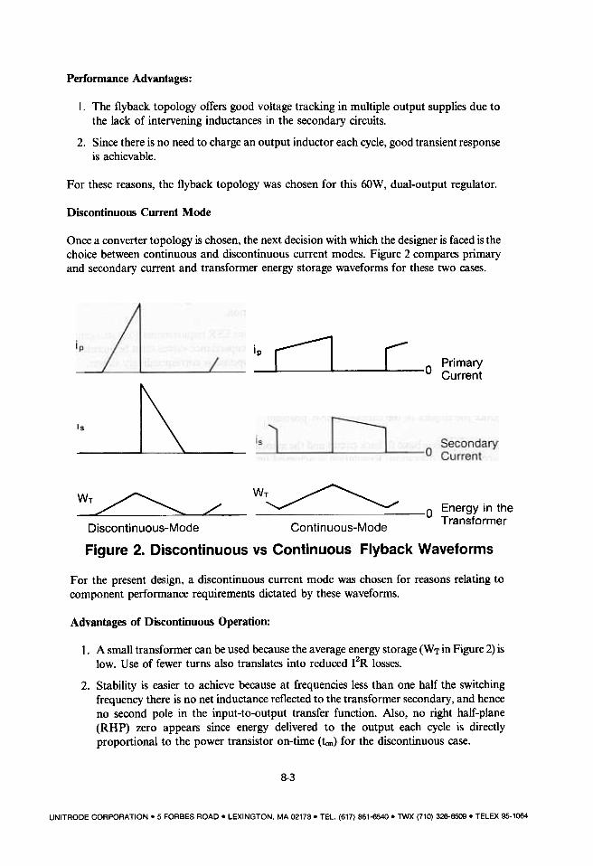
Discontinuous Current Mode
Once a converter topology is chosen, the next decision with which the designer is faced is thechoice between continuous and discontinuous current modes. Figure 2 compares primaryand secondary current and transformer energy storage waveforms for these two cases.
in .--1 ,..- Primary
~ I I 0 Current
WT~/W~ ~
Discontinuous-Mode Continuous-Mode
Figure 2. Discontinuous vs Continuous Flyback Waveforms
O Energy in the
Transformer
For the present design, a discontinuous current mode was chosen for reasons relating tocomponent performance requirements dictated by these waveforms.
Advantages of Discontinuous Operation:
I. A small transformer can be used because the average energy storage (WT in Figure 2) islow. Use of fewer turns also translates into reduced 12R losses.
2. Stability is easier to achieve because at frequencies less than one half the switchingfrequency there is no net inductance reflected to the transformer secondary, and henceno second pole in the input-to-output transfer function. Also, no right half-plane(RHP) zero appears since energy delivered to the output each cycle is directlyproportional to the power transistor on-time (100) for the discontinuous case.
8-3
UNITRODE CORPORATION. 5 FORBES ROAD. LEXINGTON, MA 02173. TEL. (617) 861-6540 .TWX (710) 326-6509 .TELEX 95-1064
3. Output rectifiers are operating at zero current just prior to becoming reverse biased.Therefore, reverse recovery requirements are not critical for these rectifiers.
4. Similarly, the power transistor turns on to a current level which is initially zero, so itsturn-on time is not critical.
5. Transistor turn-on to zero current also results in low RFI generation.
Unfortunately, some disadvantages also accrue from the use of a discontinuous current
scheme.
Disadvantages of Discontinuous Operations:
I. Transistor and diode peak current requirements are approximately twice what theywould be in a continuous mode design. Average current requirements remain
unchanged.
2. Transformer d<f>/dt and leakage inductance are both high under discontinuousoperation, resulting in some loss of cross-regulation.
3. High values of ripple current make output capacitor ESR requirements quite stringent.In most practical discontinuous flyback circuits, capacitance values must be increasedin order to achieve adequate ESR. Transient response is correspondingly slower.
In the present design, these few disadvantages were not deemed sufficient to warrant a choiceof continuous mode operation. In particular, low output current requirements (SA max.)reduce the impact of the capacitor ESR problem.
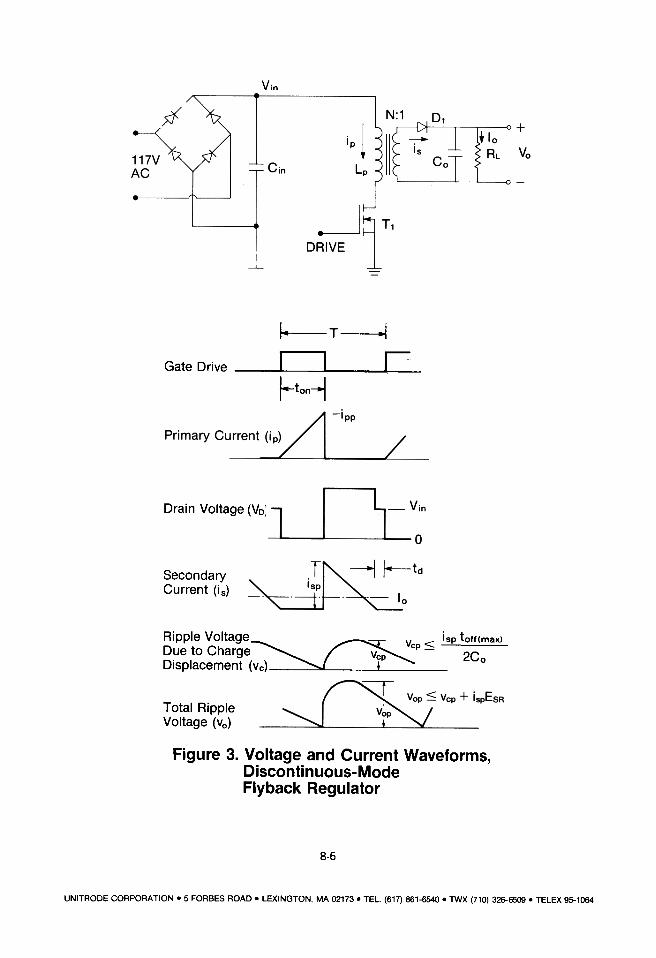
Figure 3 shows a basic flyback circuit and the associated voltage and current waveforms fordiscontinuous operation. Regulation is achieved by varying the duty cycle of power switchT 1. During the period when Ql is on, energy is transferred from input capacitor Cm to theprimary inductance Lp of the transformer. The magnitude of this stored energy is given by:
1 .2W= -Lplpp (I)
2
where ipp = peak primary current
No energy is transferred to the secondary circuit during this period. When Ql is off, energystored in the transformer is delivered by way of the secondary winding to the output filtercapacitor and load. The average power delivered to the load is given by:
.2~
2T
w
TPo= (2)
where T = switching period
8-4
UNITRODE CORPORATION. 5 FORBES ROAD. LEXINGTON, MA 02173. TEL. (617) 861-6540. TWX (710) 326-6509 .TELEX 95-1064
The peak primary current (ipp) is dependent on the input voltage (V in), the primaryinductance Lp, and the on-time of Ql (ton):
v in ton
LpIpp
Also, the average power output is related to the output voltage and load resistance:
v~Po=
Substituting for p o and ipp in equation 2, one obtains:
v~y 2 2
-= in ton
RL 2LpT
The DC output voltage is therefore:
(3)= VinD vton
T
where duty cycle D =
N ote that for a discontinuous flyback, the output voltage varies directly with both V in and
.J"RZ when a conventional PWM control chip is used.
II. SELECnON OF A CONTROL CIRCUIT
A PWM control technique is used in this design rather than a variable frequency scheme.Reasons for this decision follow, and are again related to cost and performance.
I. The transformer design can be optimized with PWM control because switching occursat a fixed frequency.
2. Fixed frequency operation results in a narrow EMI spectrum. EMI is, therefore,filterable.
3. Output ripple under light load conditions is minimized with a PWM technique.
4. Integrated circuits are available for PWM control, while variable frequency techniquesrequire discrete implementation. Modern PWM control ICs, such as the UC3840, alsoprovide various auxiliary functions which further reduce the overall number of
components required.
5. Implementation with PWM control allows for the use of a voltage-feed-forwardtechnique to achieve improved output regulation and volumetric efficiency.
6. Power supply switching can be synchronized with external circuits, such as CRTamplifiers, to reduce the display interferences.
8-5
UNITRODE CORPORATION. 5 FORBES ROAD. LEXINGTON. MA 02173. TEL. (617) 661-6540 .TWX (710) 326-6509 .TELEX 95-1064
RLT
2Lp
Vin
~
ioo--T--i
r-l CGate Drive L ~
,toni
Drain Voltage (VD)
Secondary
Current (is)
Ripple Voltage :: ~~bp ::; .::vcp < isp toff(maxl
Due to Charge Vcp -2CDisplacement (Vc) o
Total Ripple
Voltage (vo)
Figure 3. Voltage and Current Waveforms,Discontinuous-ModeFlyback Regulator
8-6
UNITRODE CORPORATION. 5 FORBES ROAD. LEXINGTON, MA 02173. TEL. (617) 861-6540 .TWX (710) 326-6509 .TELEX 95-1064
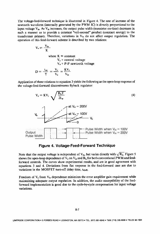
The voltage-feed-forward technique is illustrated in Figure 4. The rate of increase of thesawtooth waveform (internally generated by the PWM IC) is directly proportional to theinput voltage Vin. As Vin increases, the output pulse width (transistor on-time) decreases insuch a manner as to provide a constant "volt-second" product (constant energy) to thetransformer primary .Therefore, variations in V in do not affect output regulation. Theoperation of this feed-forward scheme is described by two relations:
V.=~K
where K = constant
V c = control voltage
V. = p- p sawtooth voltage
Vc KVcion
T
D= --
v. Vin
Application of these relations to equation 3 yields the following as the open-loop response ofthe voltage-feed-forward discontinuous flyback regulator:
(4)
Figure 4. VoItage-Feed-Forward Technique
Note that the output voltage is independent of V in, but varies directly with v-R-;; Figure 5shows the open-loop dependence of Vo on V in and RL for both conventional PWM and feed-forward controls. The curves show experimental results, and are in good agreement withequations 3 and 4. Deviations from flat response in the feed-forward case are due tovariations in the MOSFET turn-off delay time, td(off).
Freedom of Vo from V in dependence minimizes the error amplifier gain requirement whilemaintaining adequate output regulation. In addition, the audio susceptibility of the feed-
forward implementation is good due to the cycle-by-cycle compensation for input voltage
variations.
8-7
UNITRODE CORPORATION. 5 FORBES ROAD. LEXINGTON, MA 02173. TEL. (617) 861-6540 .1WX (710) 326-6509 .TELEX 95-1064
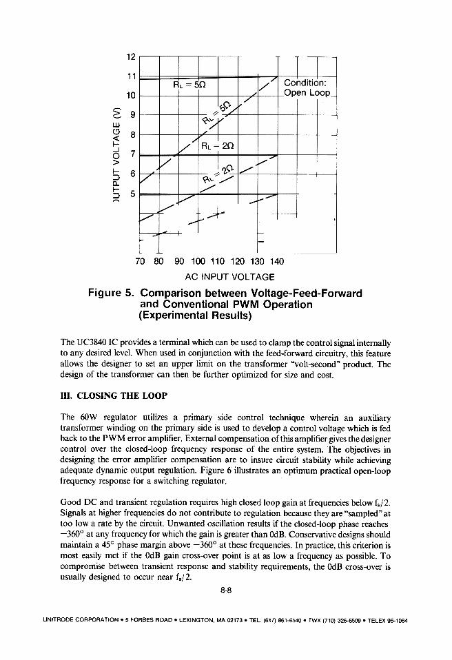
12 ~
11
10
~
LU<9~1--.JO>
1-::>0..1-::>0
9
8
7
6
5
4
3 --
2
~ I-'--' RL = 1.00 Feed-Forward
I I
-ConventionalPWM
70 80 90 100110 120130140
AC INPUT VOl TAGE
Figure 5. Comparison between VoItage-Feed-Forwardand Conventional PWM Operation
(Experimental Results)
The UC3840 IC provides a terminal which can be used to clamp the control signal internallyto any desired level. When used in conjunction with the feed-forward circuitry, this featureallows the designer to set an upper limit on the transformer "volt-second" product. Thedesign of the transformer can then be further optimized for size and cost.
III. CLOSING THE LOOP
The 6OW regulator utilizes a primary side control technique wherein an auxiliarytransformer winding on the primary side is used to develop a control voltage which is fedback to the PWM error amplifier. External compensation of this amplifier gives the designercontrol over the closed-loop frequency response of the entire system. The objectives indesigning the error amplifier compensation are to insure circuit stability while achievingadequate dynamic output regulation. Figure 6 illustrates an optimum practical open-loopfrequency response for a switching regulator.
Good DC and transient regulation requires high closed loop gain at frequencies below fs/ 2.Signals at higher frequencies do not contribute to regulation because they are "sampled" attoo Iowa rate by the circuit. Unwanted oscillation results if the closed-loop phase reaches
-360° at any frequency for which the gain is greater than OdB. Conservative designs shouldmaintain a 45° phase margin above -360° at these frequencies. In practice, this criterion ismost easily met if the OdB gain cross-over point is at as Iowa frequency as possible. To
compromise between transient response and stability requirements, the OdB cross-over is
usually designed to occur near fs/2.
8-8
UNITRODE CORPORATION. 5 FORBES ROAD. LEXINGTON, MA 02173. TEL, (617) 861-6540. TWX (710) 326-6509 .TELEX 95-1064
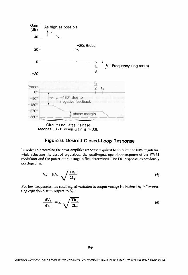
Gain
(dB)
40
-20dB/dec,20+
0,15 Frequency (109 scale)fs
2-20
Figure 6. Desired Closed-Loop Response
In order to determine the error amplifier response required to stabilize the 6OW regulator,while achieving the desired regulation, the small-signal open-loop response of the PWM
modulator and the power output stage is first determined. The DC response, as previously
developed, is:
Vo=KVc J ~
2lp
(5)
For low frequencies, the small signal variation in output voltage is obtained by differentia-ting equation 5 with respect to Vc:
dVo
dVc(6)
8-9
UNITRODE CORPORATION. 5 FORBES ROAD. LEXINGTON. MA 02173. TEL (617) 861-6540. TWX (710) 326-6509 .TELEX 95-1064
Circuit Oscillates if Phasereaches -360° when Gain is > OdB
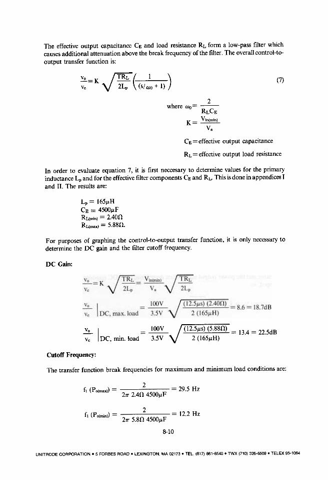
The effective output capacitance CE and load resistance RL form a low-pass filter whichcauses additional attenuation above the break frequency of the filter. The overall control-to-
output transfer function is:
Yo -K r!!!;:" i 1
~- V "2r:- \~(7)
CE = effective output capacitance
RL=effective output load resistance
In order to evaluate equation 7, it is first neccesary to determine values for the primaryinductance Lp and for the effective filter components CE and RL. This is done in appendices I
and II. The results are:
Lp = 165,uH
CE = 4500,uF
Rumin) = 2.400
Rumax) = 5.880.
For purposes of graphing the control-to-output transfer function, it is only necessary todetermine the DC gain and the fIlter cutoff frequency.
DC Gain:
Vo
Vc I DC, min. load
Cutoff Frequency:
The transfer function break frequencies for maximum and minimum load conditions are:
8-10
UNITRODE CORPORATION. 5 FORBES ROAD. LEXINGTON, MA 02173. TEL. (617) 661-6540 .TWX (710) 326-6509 .TELEX 95-1064
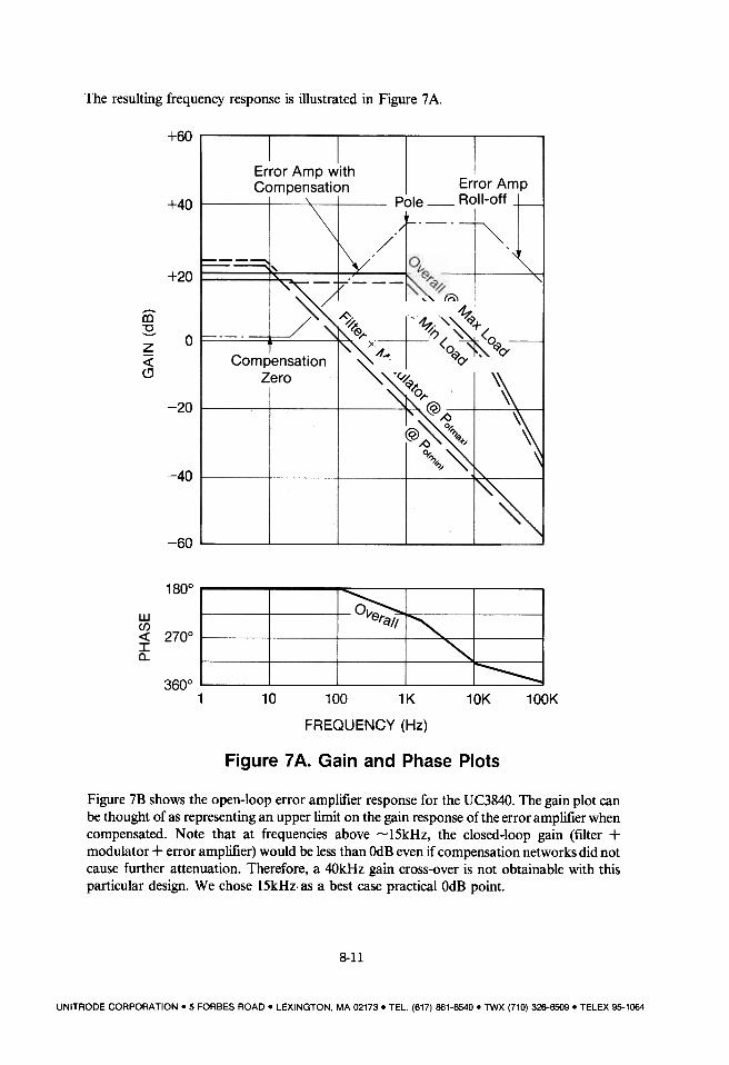
The resulting frequency response is illustrated in Figure 7 A.
+60
Error Amp with
C<:>mpensationError AmpRoll-off LPole-+40
"
cF+20
rD:3.z<{(9
~/
0
CompensationZero
-20
Ot;
'»">.1
-40
-60
180°
Overq//
~360°1 10 100 1K
FREQUENCY (Hz)
10K 100K
Figure 7 A. Gain and Phase Plots
Figure 7B shows the open-loop error amplifier response for the UC3840. The gain plot canbe thought of as representing an upper limit on the gain response of the error amplifier whencompensated. Note that at frequencies above -15kHz, the closed-loop gain (filter +modulator + error amplifier) would be less than OdB even if compensation networks did notcause further attenuation. Therefore, a 4OkHz gain cross-over is not obtainable with thisparticular design. We chose l5kHz. as a best case practical OdB point.
8-11
UNITRODE CORPORATION. 5 FORBES ROAD. LEXINGTON, MA 02173. TEL. (617) 661-6540. TWX (710) 326-6509 .TELEX 95-1064
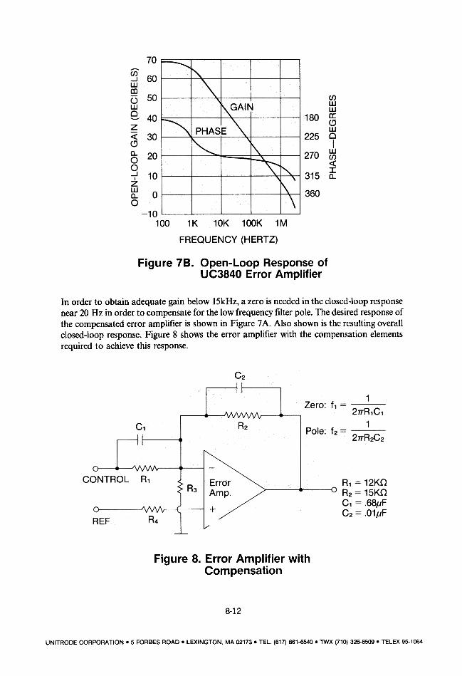
Figure 78. Open-Loop Response ofUC3840 Error Amplifier
In order to obtain adequate gain below lSkHz, a zero is needed in the closed-loop responsenear 20 Hz in order to compensate for the low frequency filter pole. The desired response ofthe compensated error amplifier is shown in Figure 7 A. Also shown is the resulting overallclosed-loop response. Figure 8 shows the error amplifier with the compensation elementsrequired to achieve this response.
Figure 8. Error Amplifier withCompensation
8-12
UNITRODE CORPORATION 0 5 FORBES ROAD 0 LEXINGTON. MA 02173 0 TEL. (617) 861-6540 o1WX (710) 326-6509 0 TELEX 95-1064
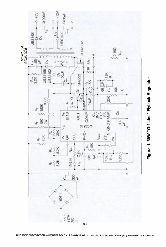
IV. DESIGN DETAILS AND PERFORMANCE (Refer to Figure I)
The AC input voltage for this supply is rectified with a full-wave bridge and filtered by inputcapacitor Cn. The UC3840 control chip is equipped with under- and over-voltage lockoutfeatures. The under-voltage feature initially disables all internal circuits except the (lowcurrent) reference voltage circuit. The lockout voltage is set by divider network ~-~-~ inFigure I. This feature allows capacitor CA to charge through ~ and to store enough energyto power the drive circuitry. The UC3840 under-voltage lockout has built-in hysteresis toprevent hesitant start-up.
After the control IC is enabled, drive energy is provided each cycle from an auxiliary primaryside transformer winding W 1. In conjunction with CA and diode Dl, this winding forms aregulated 12V drive supply. This supply is also used to provide primary-side control for the 5and 12V outputs. This voltage is fed to the UC3840 control input through Rl. This low-costcontrol scheme is not optimum in terms of output coupling, but, with a careful transformerdesign, :t2% regulation is still achievable.
The u C3840 operates at a fixed frequency f. = 1/ (RM). This frequency is independent of
the ramp slope, which varies directly with input voltage V in, to provide voltage-feed-forwardcompensation. This ramp slope variation is accomplished as follows. Control chip input V. isno more than one forward-biased diode drop above ground. Therefore, the current throughR9 is almost directly proportional to V in. This current is fed internally to a current mirrorwhich in turn drives ramp-control capacitor CR at a charging rate proportional to Vin. Ramplinearity is better than 2%.
In order to optimize the transformer, it is desirable to limit the maximum duty cycle, aspreviously mentioned. This is accomplished with the UC3840 by clamping the control
voltage to a level determined by voltage divider R7-Rlo and diode O2.
Transistor Q2 and diode 03 provide a low impedance drive for fast switching of power FET
Ql. An internal transistor always pulls the UC3840 bias output to a level near supply voltage
V c unless the under-voltage lockout is active. When the open-collector control chip output ishigh, then drive to Q2 is provided from the bias output through Rll. In this way the input
capacitance of Ql is quickly charged for fast turn-on. This input capacitance is discharged
through 03 at turn-off.
The UC3840 also provides dynamic current limiting to protect costly power components.Primary current flows through R12 to develop a current-limit input signal at point A. This
signal is compared to a reference signal established by R15 and R3. When the current-limitsignal exceeds this reference by 4OOm V, an internal error latch forces the PWM output low
but leaves the bias output enabled. Capacitor CA discharges through Ru until the under-voltage feature is activated, turning off the bias transistor. Not until this time does the control
chip attempt a restart.
The snubber network R14-CTD4 prevents turn-off voltage spikes from exceeding the FETbreakdown voltage. This snubber does not provide load-Iine shaping.
Power FET Ql and output rectifiers 05 and 06 are all in TO-220 packages to provide highvolumetric efficiency. The rectifiers were chosen for fast forward recovery to minimize
8-13
UNITRODE CORPORATION. 5 FORBES ROAD. LEXINGTON, MA 02173. TEL (617) 861-6540 .TWX (710) 326-6509 .TELEX 95-1064
switching losses. The higher-current SV output utilizes a Schottky rectifier for low forward-biased power dissipation. The power PET provides fast switching when driven with thesimple, efficient circuit already described.
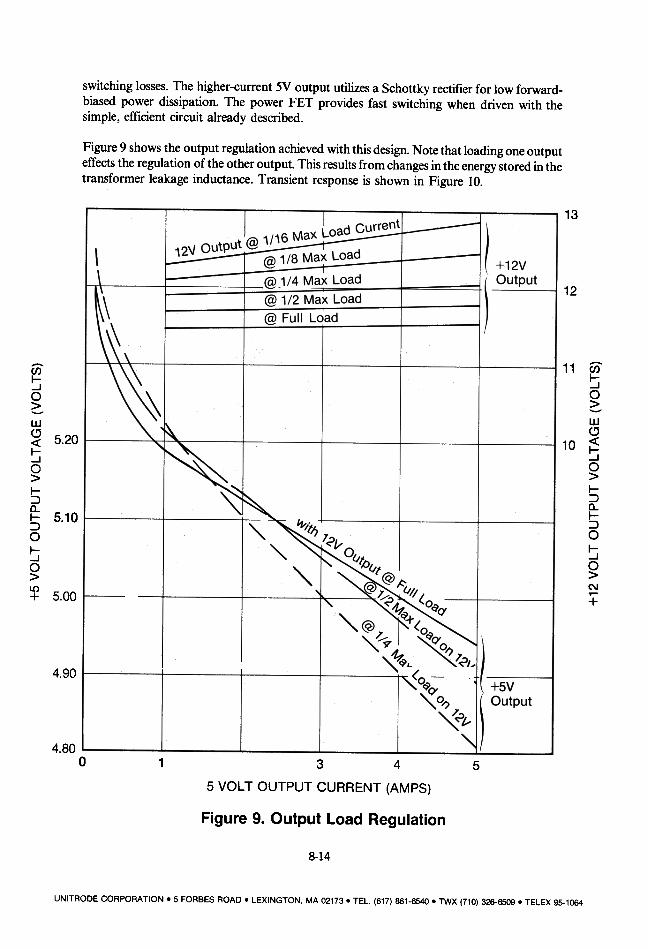
Figure 9 shows the output regulation achieved with this design. Note that loading one outputeffects the regulation of the other output. This results from changes in the energy stored in thetransformer leakage inductance. Transient response is shown in Figure 10.
1312V output @1/16 Max Load Currenl
+12V\( Output
12
~~\
--
~-@-1/4 Max Load:.-@ 1/2 Max Load
I@ Full Load
\\
11 ffj
-.JOC:.w~
10 ~-.J0>1-=>c..1-=>01--.J0>(\I.-+
,,
001--.JOGw"«1--.J0>1-~Q.1-~0
~0>I/)+
If,.tii)~""' ~
~ VI; ~ -
~ OqQ'"'
" (§) ?~,
,
,( ':::':Q'-
Qo.J..I
4.90+5VOutput
4.800 1 3 4
5 VOl T OUTPUT CURRENT (AMPS)
5
Figure 9. Output Load Regulation
8-14
UNITRODE CORPORATION. 5 FORBES ROAD. LEXINGTON, MA 02173. TEL. (617) 661-6540 .TWX (710) 326-6509 .TELEX 95-1064
5.20
5.10
5.00

Yo
Vos
io
0
Figure 10A. Drain Voltage andCurrent Waveform Showingthe Effect of theDe-Spiking Network
Figure 108. Transient Response:Step Change of LoadCurrent from 1A to 3Ain +12V Output
8-15
UNITRODE CORPORATION. 5 FORBES ROAD. LEXINGTON, MA 02173. TEL. (617) 861-6540 .TWX (710) 326-6509 .TELEX 9&-1064

IMPORTANT NOTICE
Texas Instruments and its subsidiaries (TI) reserve the right to make changes to their products or to discontinueany product or service without notice, and advise customers to obtain the latest version of relevant informationto verify, before placing orders, that information being relied on is current and complete. All products are soldsubject to the terms and conditions of sale supplied at the time of order acknowledgment, including thosepertaining to warranty, patent infringement, and limitation of liability.
TI warrants performance of its products to the specifications applicable at the time of sale in accordance withTI’s standard warranty. Testing and other quality control techniques are utilized to the extent TI deems necessaryto support this warranty. Specific testing of all parameters of each device is not necessarily performed, exceptthose mandated by government requirements.
Customers are responsible for their applications using TI components.
In order to minimize risks associated with the customer’s applications, adequate design and operatingsafeguards must be provided by the customer to minimize inherent or procedural hazards.
TI assumes no liability for applications assistance or customer product design. TI does not warrant or representthat any license, either express or implied, is granted under any patent right, copyright, mask work right, or otherintellectual property right of TI covering or relating to any combination, machine, or process in which suchproducts or services might be or are used. TI’s publication of information regarding any third party’s productsor services does not constitute TI’s approval, license, warranty or endorsement thereof.
Reproduction of information in TI data books or data sheets is permissible only if reproduction is withoutalteration and is accompanied by all associated warranties, conditions, limitations and notices. Representationor reproduction of this information with alteration voids all warranties provided for an associated TI product orservice, is an unfair and deceptive business practice, and TI is not responsible nor liable for any such use.
Resale of TI’s products or services with statements different from or beyond the parameters stated by TI forthat product or service voids all express and any implied warranties for the associated TI product or service,is an unfair and deceptive business practice, and TI is not responsible nor liable for any such use.
Also see: Standard Terms and Conditions of Sale for Semiconductor Products. www.ti.com/sc/docs/stdterms.htm
Mailing Address:
Texas InstrumentsPost Office Box 655303Dallas, Texas 75265
Copyright 2001, Texas Instruments Incorporated