Embed Size (px)
Citation preview

Switched-mode power supply charger
Aarne Liski
Jere Kinnunen
Final presentation
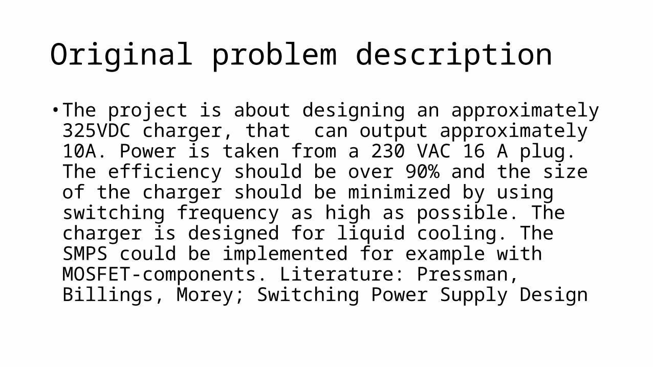
Original problem description
• The project is about designing an approximately 325VDC charger, that can output approximately 10A. Power is taken from a 230 VAC 16 A plug. The efficiency should be over 90% and the size of the charger should be minimized by using switching frequency as high as possible. The charger is designed for liquid cooling. The SMPS could be implemented for example with MOSFET-components. Literature: Pressman, Billings, Morey; Switching Power Supply Design
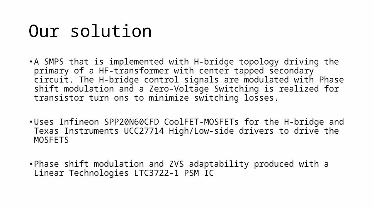
Our solution
• A SMPS that is implemented with H-bridge topology driving the primary of a HF-transformer with center tapped secondary circuit. The H-bridge control signals are modulated with Phase shift modulation and a Zero-Voltage Switching is realized for transistor turn ons to minimize switching losses.
• Uses Infineon SPP20N60CFD CoolFET-MOSFETs for the H-bridge and Texas Instruments UCC27714 High/Low-side drivers to drive the MOSFETS
• Phase shift modulation and ZVS adaptability produced with a Linear Technologies LTC3722-1 PSM IC
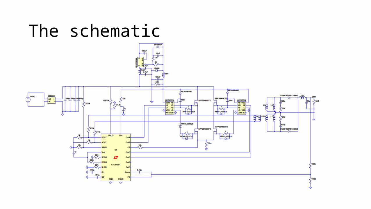
The schematic
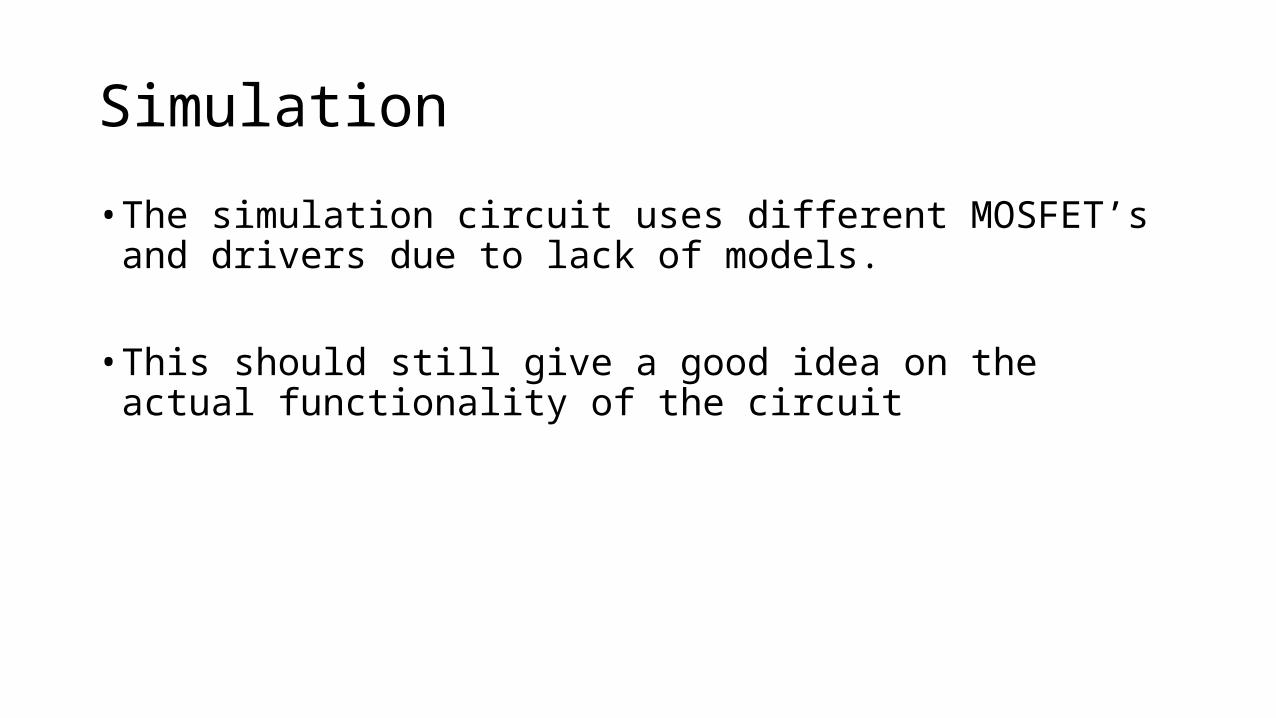
Simulation
• The simulation circuit uses different MOSFET’s and drivers due to lack of models.
• This should still give a good idea on the actual functionality of the circuit
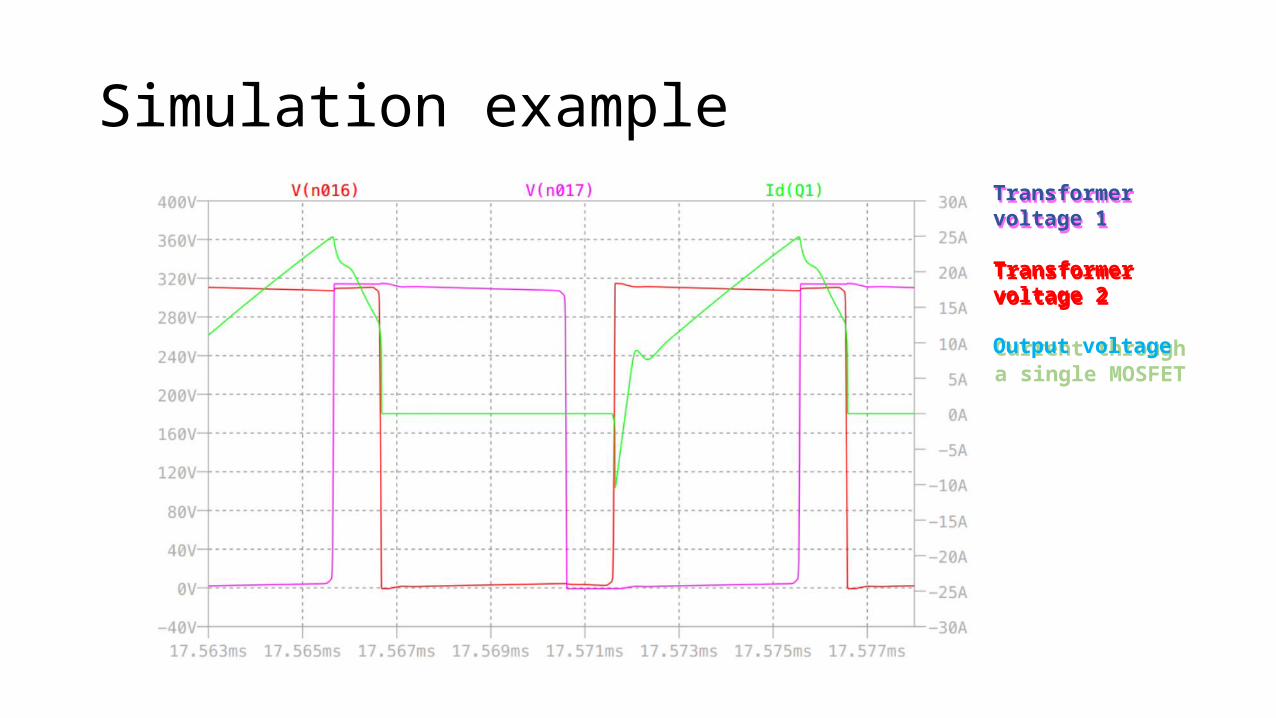
Simulation exampleTransformer voltage 1
Transformer voltage 2
Current through a single MOSFET
Transformer voltage 1
Transformer voltage 2
Output voltage
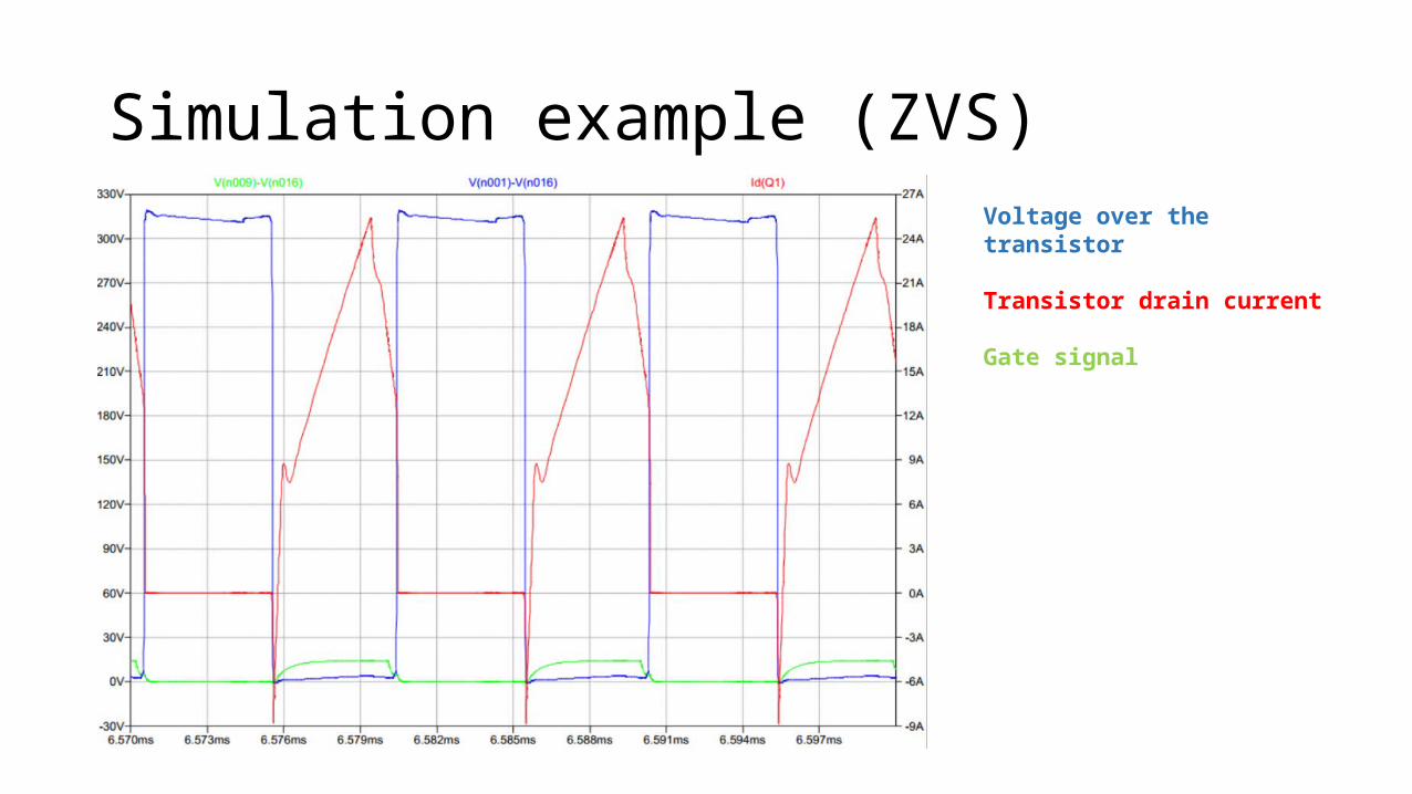
Simulation example (ZVS)Voltage over the transistor
Transistor drain current
Gate signal
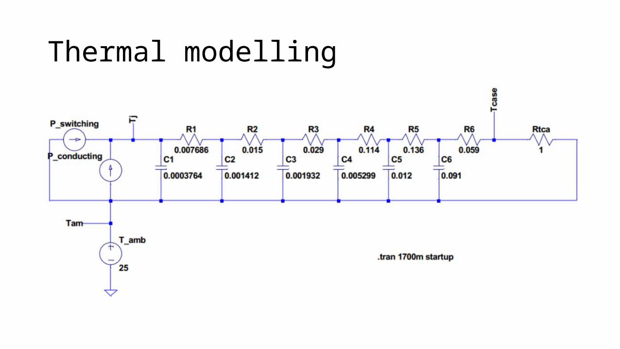
Thermal modelling
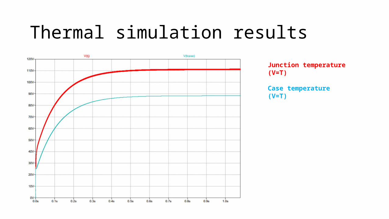
Thermal simulation results
Junction temperature (V=T)
Case temperature (V=T)
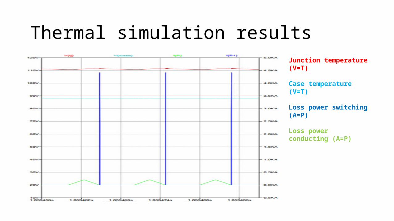
Thermal simulation resultsJunction temperature (V=T)
Case temperature (V=T)
Loss power switching (A=P)
Loss power conducting (A=P)
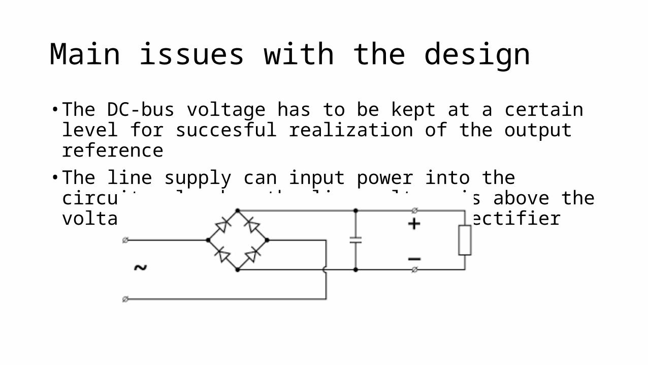
Main issues with the design
• The DC-bus voltage has to be kept at a certain level for succesful realization of the output reference• The line supply can input power into the circuit only when the line
voltage is above the voltage of the output of the input rectifier
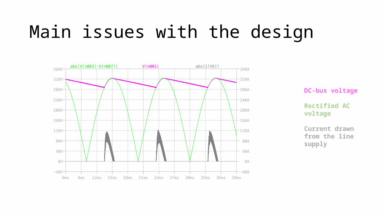
Main issues with the design
DC-bus voltage
Rectified AC voltage
Current drawn from the line supply
Main issues with the design
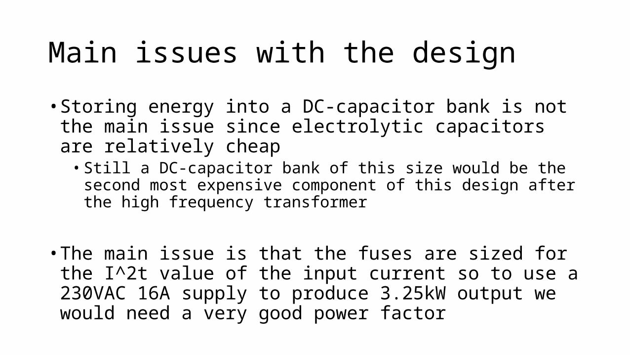
• Storing energy into a DC-capacitor bank is not the main issue since electrolytic capacitors are relatively cheap • Still a DC-capacitor bank of this size would be the second most expensive
component of this design after the high frequency transformer
• The main issue is that the fuses are sized for the I^2t value of the input current so to use a 230VAC 16A supply to produce 3.25kW output we would need a very good power factor
Proposed modifications to current design• There were two solutions proposed in order to lengthen the time
during which energy can be drawn from the line input and to increase the power factor
• 1. Increase the transformer ratio to allow for lower DC-bus voltage
• 2 Use a passive choke to aid storing energy and correct the power factor
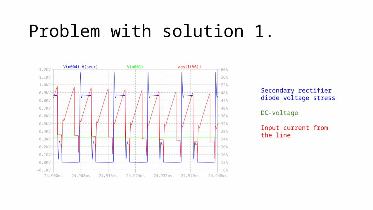
Problem with solution 1.
• Because of the increased turns ratio the secondary side rectifier diodes need to withstand huge voltages when the input is highest (close to 325VDC)
• 1.2kV is a practical limit with stock-made components that are feasibly priced considering this application• The max input current was still over 45 amps when this limit was reached
Problem with solution 1.
Secondary rectifier diode voltage stress
DC-voltage
Input current from the line
Problem with solution 2. (choke)
• Passive chokes are very bulky and expensive
• Choke of this size would also introduce considerable losses
• Chokes of this size are not made to stock
• The goal was to design a SMPS that is affordable, lightweight and small and this solution is none of these
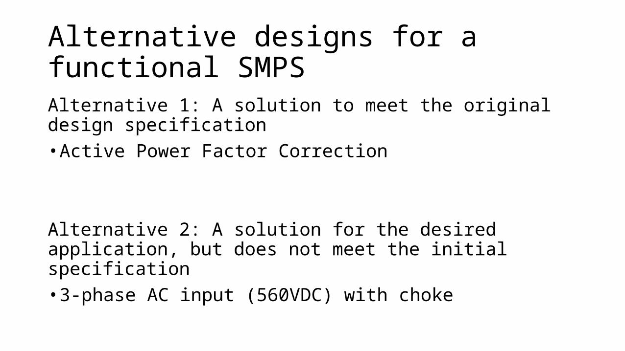
Alternative designs for a functional SMPSAlternative 1: A solution to meet the original design specification• Active Power Factor Correction
Alternative 2: A solution for the desired application, but does not meet the initial specification• 3-phase AC input (560VDC) with choke
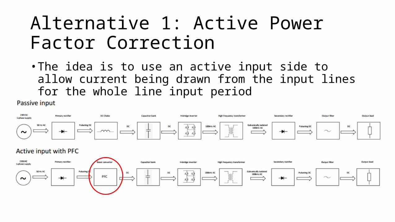
Alternative 1: Active Power Factor Correction• The idea is to use an active input side to allow current being drawn
from the input lines for the whole line input period
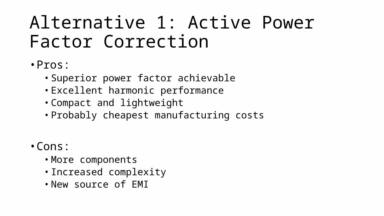
Alternative 1: Active Power Factor Correction• Pros:• Superior power factor achievable• Excellent harmonic performance • Compact and lightweight• Probably cheapest manufacturing costs
• Cons:• More components• Increased complexity• New source of EMI
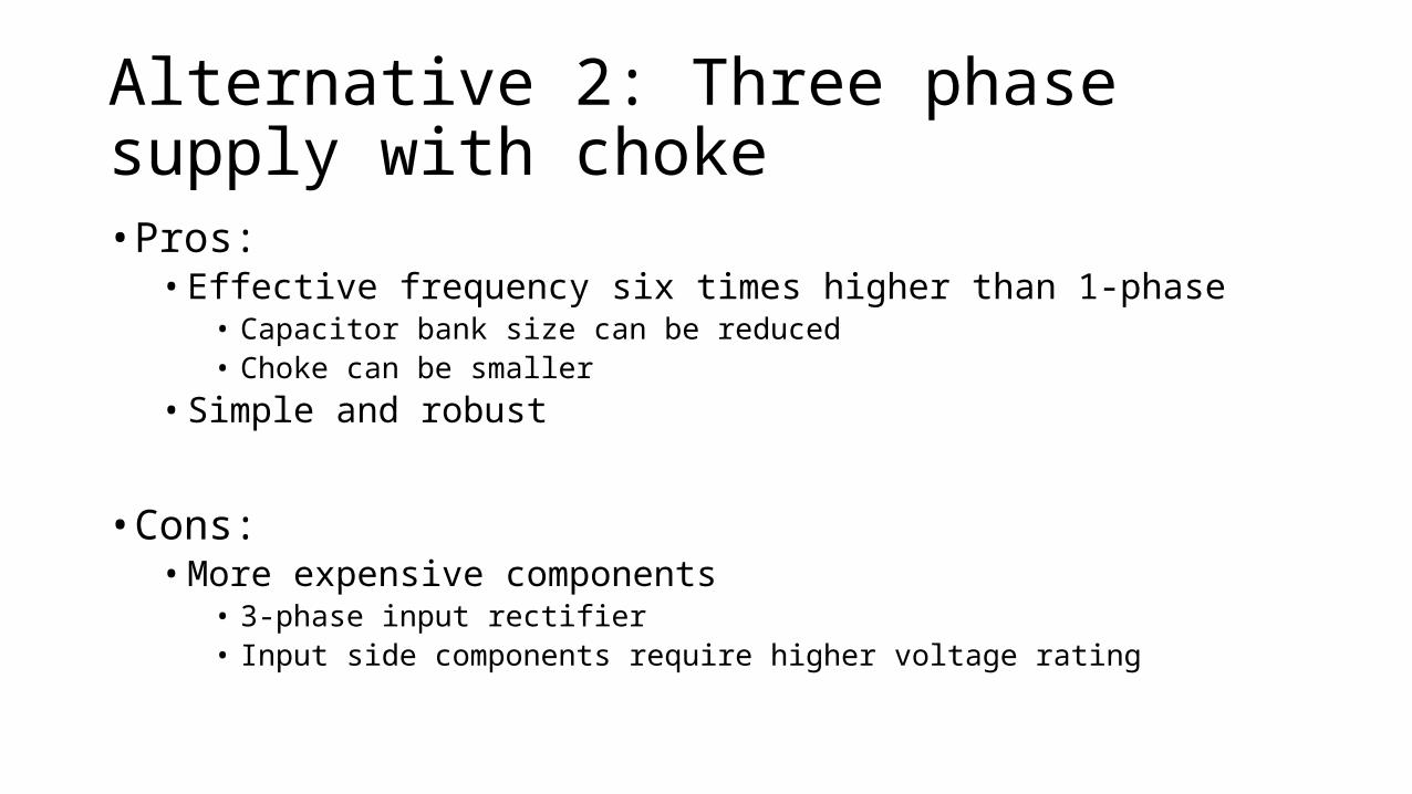
Alternative 2: Three phase supply with choke• Pros:• Effective frequency six times higher than 1-phase
• Capacitor bank size can be reduced• Choke can be smaller
• Simple and robust
• Cons:• More expensive components
• 3-phase input rectifier• Input side components require higher voltage rating
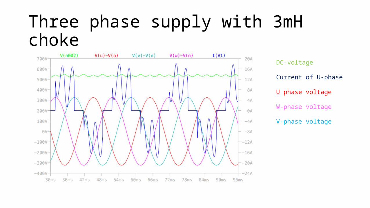
Three phase supply with 3mH choke
DC-voltage
Current of U-phase
U phase voltage
W-phase voltage
V-phase voltage
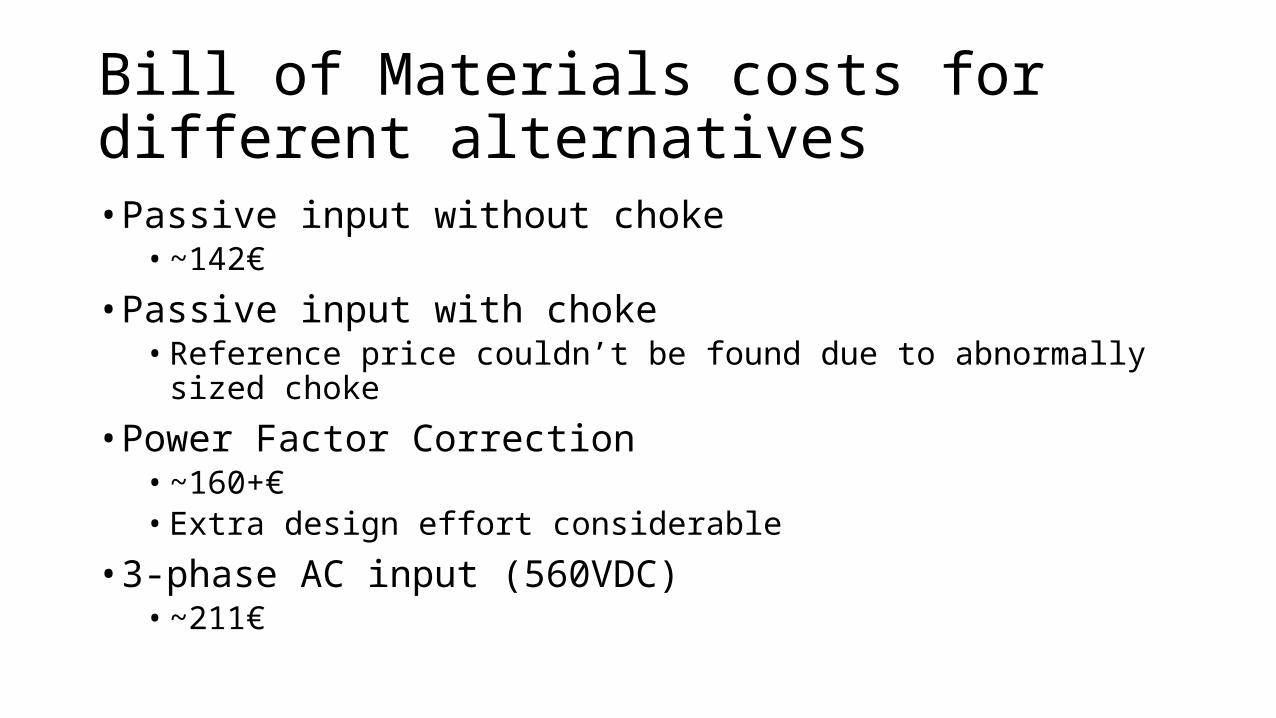
Bill of Materials costs for different alternatives• Passive input without choke• ~142€
• Passive input with choke• Reference price couldn’t be found due to abnormally sized choke
• Power Factor Correction• ~160+€ • Extra design effort considerable
• 3-phase AC input (560VDC)• ~211€
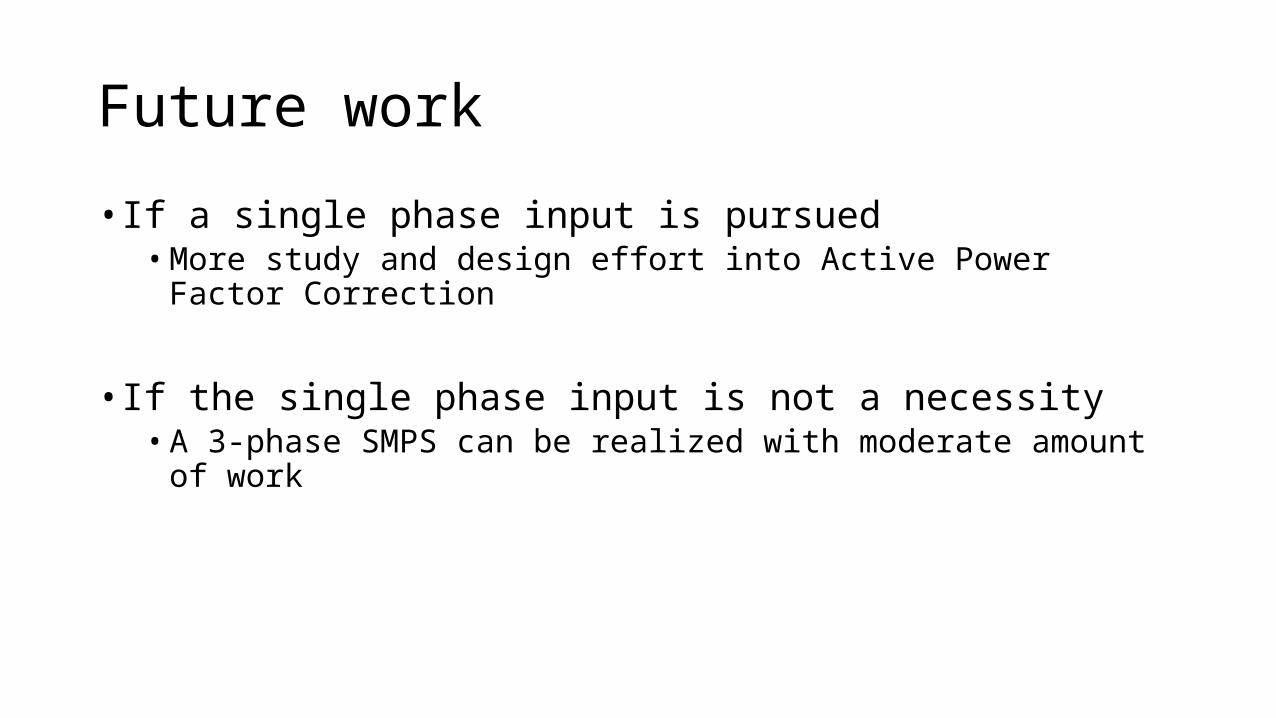
Future work
• If a single phase input is pursued• More study and design effort into Active Power Factor Correction
• If the single phase input is not a necessity• A 3-phase SMPS can be realized with moderate amount of work
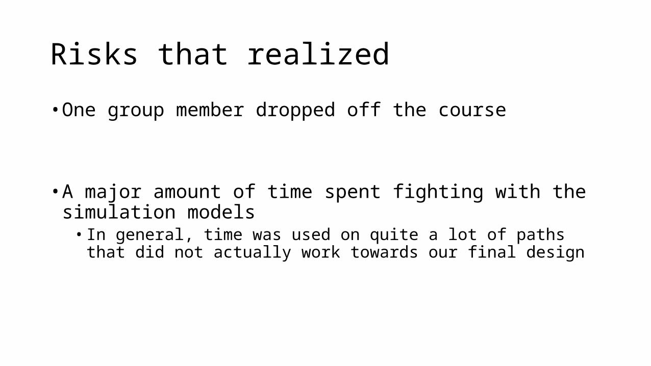
Risks that realized
• One group member dropped off the course
• A major amount of time spent fighting with the simulation models• In general, time was used on quite a lot of paths that did not actually work
towards our final design
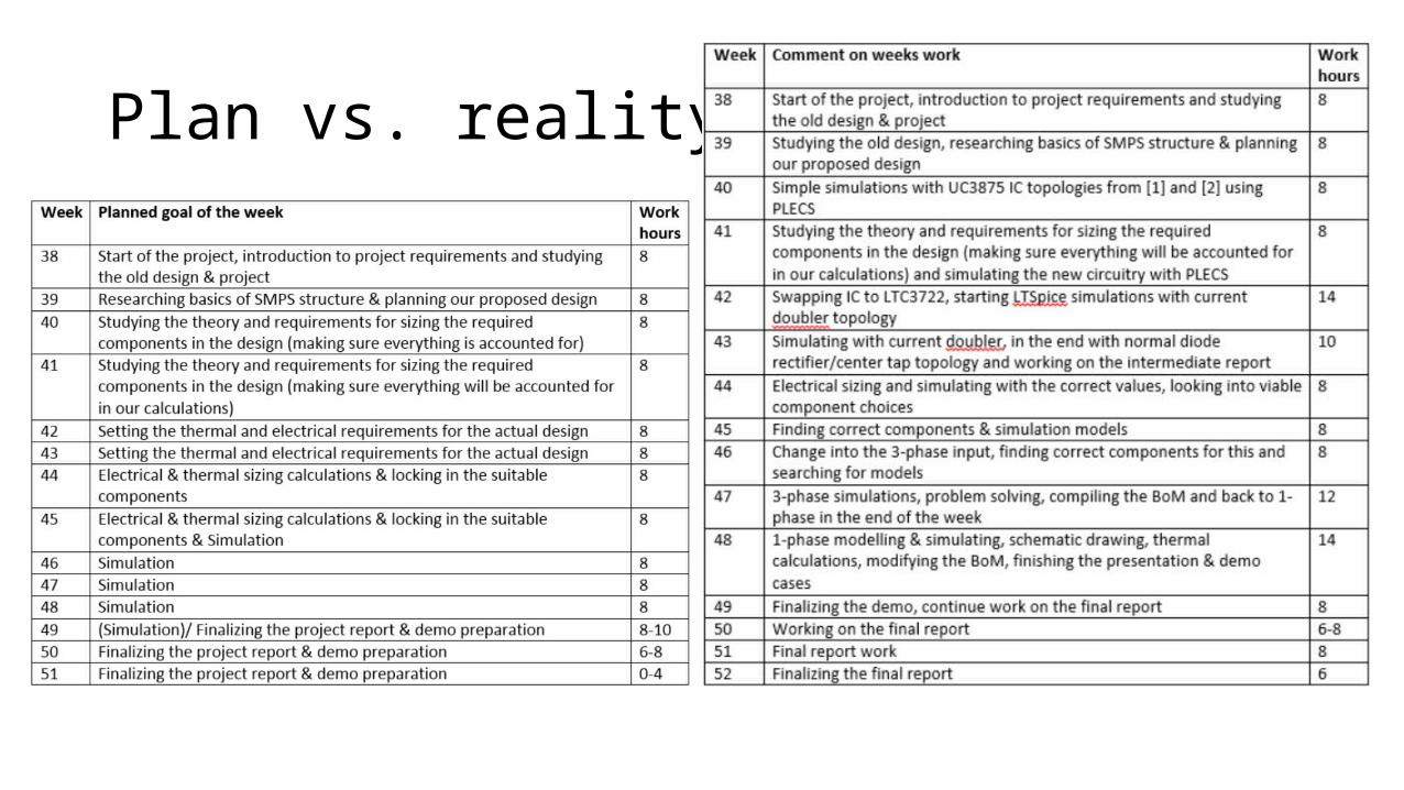
Plan vs. reality

Questions?