Embed Size (px)
Citation preview

1
© 2008 Microchip Technology Incorporated. All Rights Reserved. Switch Mode Power Supply Topologies Slide 1
Switch Mode Power Supply Topologies
The Forward Converter
Welcome to this Web seminar on Switch Mode Power Supply Topologies. In this webinar, we will analyze the Forward Converter. It is a transformer-isolated converter, based on the basic buck converter topology.

2
© 2008 Microchip Technology Incorporated. All Rights Reserved. Switch Mode Power Supply Topologies Slide 2
Topics
• Forward Converter Basics
• Circuit Operation
• Design Equations
We will start with a brief description of the basic operation of the converter. We will then analyze the behaviour of the system in its various operating conditions, and we will derive the basic equations. We will then analyze how to determine and select the components to build such a converter.

3
© 2008 Microchip Technology Incorporated. All Rights Reserved. Switch Mode Power Supply Topologies Slide 3
Forward Converter
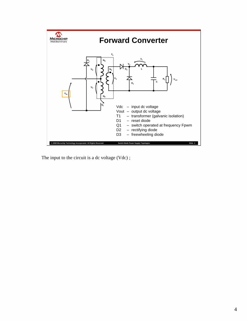
Vdc – input dc voltageVout – output dc voltageT1 – transformer (galvanic isolation)D1 – reset diodeQ1 – switch operated at frequency FpwmD2 – rectifying diodeD3 – freewheeling diode
NR
NP
NS
D1
D2
D3
L
CRo Vout
VP
VR
VS
Q1
VL
Vdc
VV22
TT11
This is the basic circuit of a forward converter.
4
© 2008 Microchip Technology Incorporated. All Rights Reserved. Switch Mode Power Supply Topologies Slide 4
Forward Converter
Vdc – input dc voltageVout – output dc voltageT1 – transformer (galvanic isolation)D1 – reset diodeQ1 – switch operated at frequency FpwmD2 – rectifying diodeD3 – freewheeling diode
NR
NP
NS
D1
D2
D3
L
CRo Vout
VP
VR
VS
Q1
VL
Vdc
VV22
TT11
The input to the circuit is a dc voltage (Vdc) ;
5
© 2008 Microchip Technology Incorporated. All Rights Reserved. Switch Mode Power Supply Topologies Slide 5
Forward Converter
Vdc – input dc voltageVout – output dc voltageT1 – transformer (galvanic isolation)D1 – reset diodeQ1 – switch operated at frequency FpwmD2 – rectifying diodeD3 – freewheeling diode
NR
NP
NS
D1
D2
D3
L
CRo Vout
VP
VR
VS
Q1
VL
Vdc
VV22
TT11
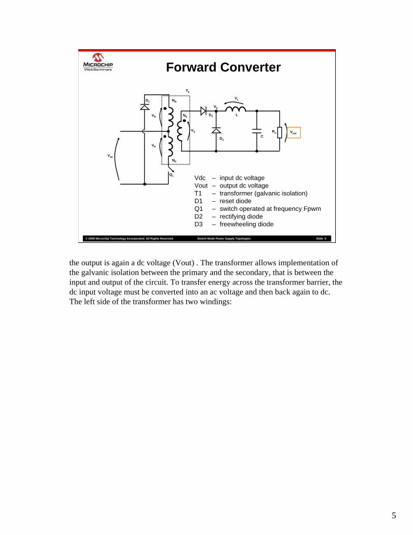
the output is again a dc voltage (Vout) . The transformer allows implementation of the galvanic isolation between the primary and the secondary, that is between the input and output of the circuit. To transfer energy across the transformer barrier, the dc input voltage must be converted into an ac voltage and then back again to dc. The left side of the transformer has two windings:

6
© 2008 Microchip Technology Incorporated. All Rights Reserved. Switch Mode Power Supply Topologies Slide 6
Forward Converter
Vdc – input dc voltageVout – output dc voltageT1 – transformer (galvanic isolation)D1 – reset diodeQ1 – switch operated at frequency FpwmD2 – rectifying diodeD3 – freewheeling diode
NR
NP
NS
D1
D2
D3
L
CRo Vout
VP
VR
VS
Q1
VL
Vdc
VV22
TT11
Np is the primary winding ,
7
© 2008 Microchip Technology Incorporated. All Rights Reserved. Switch Mode Power Supply Topologies Slide 7
Forward Converter
Vdc – input dc voltageVout – output dc voltageT1 – transformer (galvanic isolation)D1 – reset diodeQ1 – switch operated at frequency FpwmD2 – rectifying diodeD3 – freewheeling diode
NR
NP
NS
D1
D2
D3
L
CRo Vout
VP
VR
VS
Q1
VL
Vdc
VV22
TT11
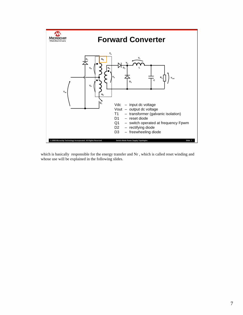
which is basically responsible for the energy transfer and Nr , which is called reset winding and whose use will be explained in the following slides.
8
© 2008 Microchip Technology Incorporated. All Rights Reserved. Switch Mode Power Supply Topologies Slide 8
Forward Converter
Vdc – input dc voltageVout – output dc voltageT1 – transformer (galvanic isolation)D1 – reset diodeQ1 – switch operated at frequency FpwmD2 – rectifying diodeD3 – freewheeling diode
NR
NP
NS
D1
D2
D3
L
CRo Vout
VP
VR
VS
Q1
VL
Vdc
VV22
TT11
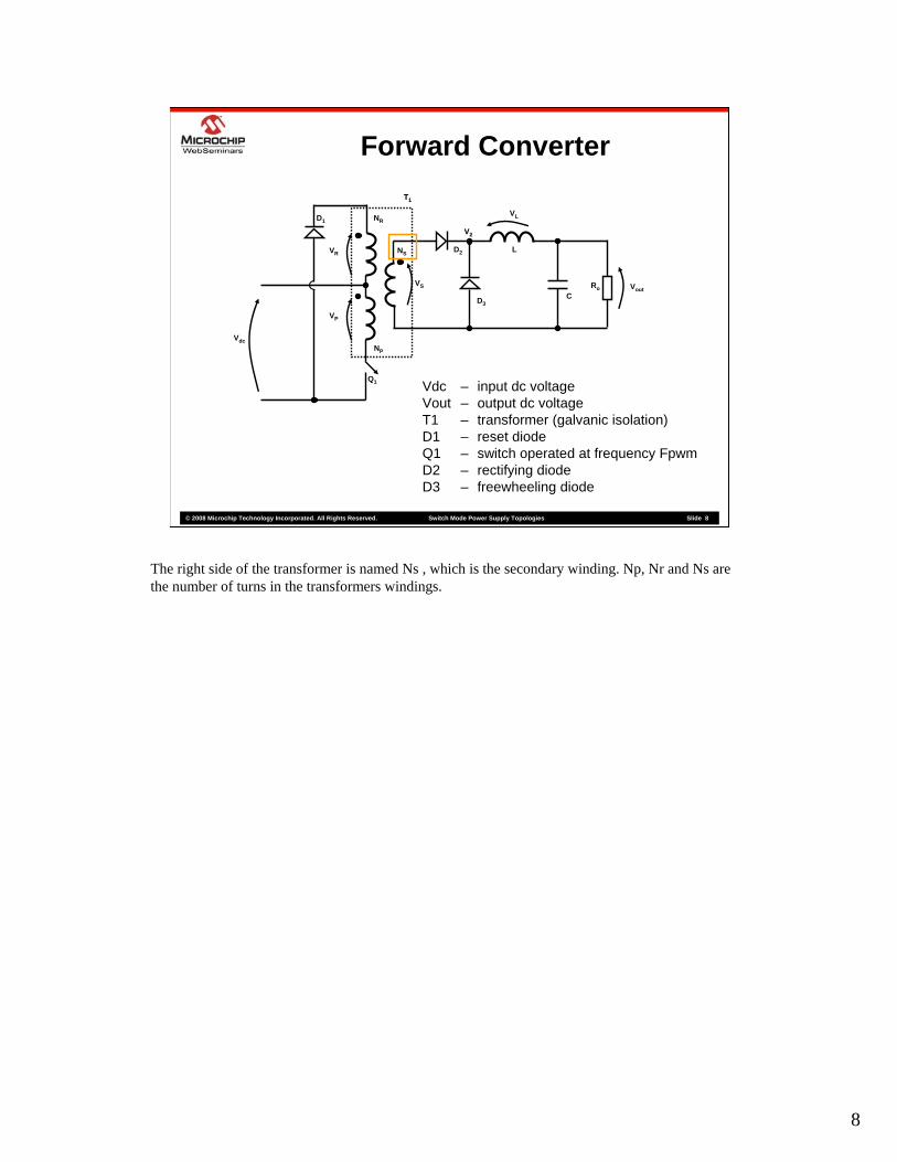
The right side of the transformer is named Ns , which is the secondary winding. Np, Nr and Ns are the number of turns in the transformers windings.

9
© 2008 Microchip Technology Incorporated. All Rights Reserved. Switch Mode Power Supply Topologies Slide 9
Forward Converter
Vdc – input dc voltageVout – output dc voltageT1 – transformer (galvanic isolation)D1 – reset diodeQ1 – switch operated at frequency FpwmD2 – rectifying diodeD3 – freewheeling diode
NR
NP
NS
D1
D2
D3
L
CRo Vout
VP
VR
VS
Q1
VL
Vdc
VV22
TT11
Diode D1 is used, with Nr, to create a path to discharge the energy stored into the transformer while the switch is open.
10
© 2008 Microchip Technology Incorporated. All Rights Reserved. Switch Mode Power Supply Topologies Slide 10
Forward Converter
Vdc – input dc voltageVout – output dc voltageT1 – transformer (galvanic isolation)D1 – reset diodeQ1 – switch operated at frequency FpwmD2 – rectifying diodeD3 – freewheeling diode
NR
NP
NS
D1
D2
D3
L
CRo Vout
VP
VR
VS
Q1
VL
Vdc
VV22
TT11
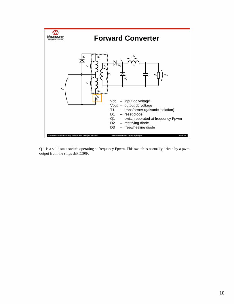
Q1 is a solid state switch operating at frequency Fpwm. This switch is normally driven by a pwm output from the smps dsPIC30F.

11
© 2008 Microchip Technology Incorporated. All Rights Reserved. Switch Mode Power Supply Topologies Slide 11
Forward Converter
Vdc – input dc voltageVout – output dc voltageT1 – transformer (galvanic isolation)D1 – reset diodeQ1 – switch operated at frequency FpwmD2 – rectifying diodeD3 – freewheeling diode
NR
NP
NS
D1
D2
D3
L
CRo Vout
VP
VR
VS
Q1
VL
Vdc
VV22
TT11
Diodes D2 and D3 rectify the secondary voltage; diode D3 is commonly called a freewheeling diode.
12
© 2008 Microchip Technology Incorporated. All Rights Reserved. Switch Mode Power Supply Topologies Slide 12
Forward Converter
Vdc – input dc voltageVout – output dc voltageT1 – transformer (galvanic isolation)D1 – reset diodeQ1 – switch operated at frequency FpwmD2 – rectifying diodeD3 – freewheeling diode
NR
NP
NS
D1
D2
D3
L
CRo Vout
VP
VR
VS
Q1
VL
Vdc
VV22
TT11
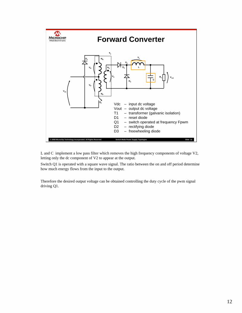
L and C implement a low pass filter which removes the high frequency components of voltage V2, letting only the dc component of V2 to appear at the output.Switch Q1 is operated with a square wave signal. The ratio between the on and off period determine how much energy flows from the input to the output.
Therefore the desired output voltage can be obtained controlling the duty cycle of the pwm signal driving Q1.
13
© 2008 Microchip Technology Incorporated. All Rights Reserved. Switch Mode Power Supply Topologies Slide 13
Forward Converter
NR
NP
NS
D1
D2
D3
L
CRo Vout
VP
VR
VS
Q1
VL
Vdc
TONTOFF
T
Q1command
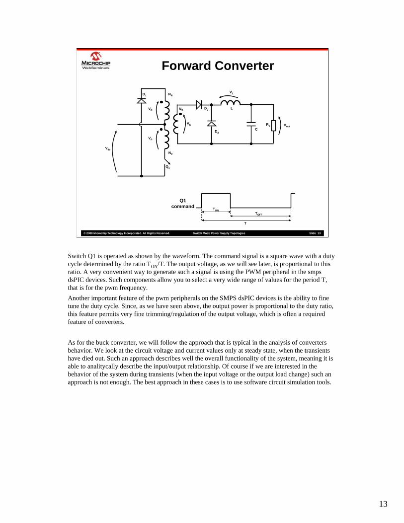
Switch Q1 is operated as shown by the waveform. The command signal is a square wave with a duty cycle determined by the ratio TON/T. The output voltage, as we will see later, is proportional to this ratio. A very convenient way to generate such a signal is using the PWM peripheral in the smps dsPIC devices. Such components allow you to select a very wide range of values for the period T, that is for the pwm frequency.Another important feature of the pwm peripherals on the SMPS dsPIC devices is the ability to fine tune the duty cycle. Since, as we have seen above, the output power is proportional to the duty ratio, this feature permits very fine trimming/regulation of the output voltage, which is often a required feature of converters.
As for the buck converter, we will follow the approach that is typical in the analysis of converters behavior. We look at the circuit voltage and current values only at steady state, when the transients have died out. Such an approach describes well the overall functionality of the system, meaning it is able to analitycally describe the input/output relationship. Of course if we are interested in the behavior of the system during transients (when the input voltage or the output load change) such an approach is not enough. The best approach in these cases is to use software circuit simulation tools.
14
© 2008 Microchip Technology Incorporated. All Rights Reserved. Switch Mode Power Supply Topologies Slide 14
Forward ConverterNR
NP
NS
D1
D2
D3
L
CRo Vout
VP
VR
VS
Q1
VL
Vdc
P
S
P
S
NN
VV
=
Transformer Basic Equations
S
P
P
S
NN
II
=
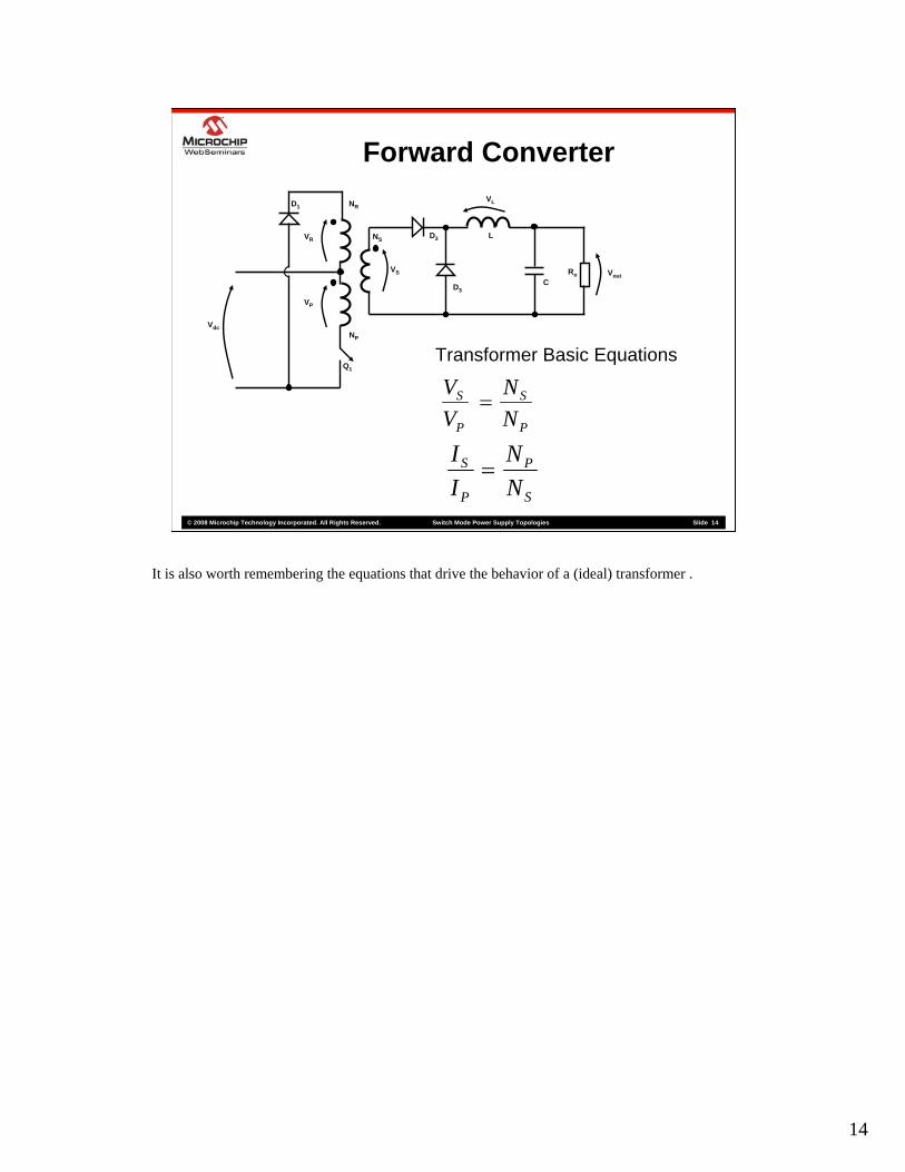
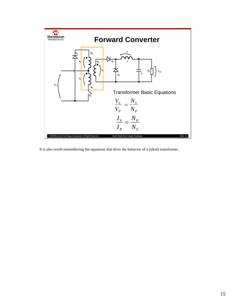
It is also worth remembering the equations that drive the behavior of a (ideal) transformer .
15
© 2008 Microchip Technology Incorporated. All Rights Reserved. Switch Mode Power Supply Topologies Slide 15
Forward ConverterNR
NP
NS
D1
D2
D3
L
CRo Vout
VP
VR
VS
Q1
VL
Vdc
P
S
P
S
NN
VV
=
Transformer Basic Equations
S
P
P
S
NN
II
=
It is also worth remembering the equations that drive the behavior of a (ideal) transformer .
16
© 2008 Microchip Technology Incorporated. All Rights Reserved. Switch Mode Power Supply Topologies Slide 16
Forward ConverterNR
NP
NS
D1
D2
D3
L
CRo Vout
VP
VR
VS
Q1
VL
Vdc
P
S
P
S
NN
VV
=
Transformer Basic Equations
S
P
P
S
NN
II
=
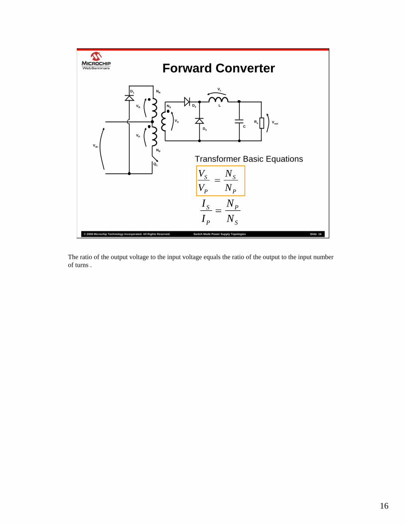
The ratio of the output voltage to the input voltage equals the ratio of the output to the input number of turns .
17
© 2008 Microchip Technology Incorporated. All Rights Reserved. Switch Mode Power Supply Topologies Slide 17
Forward ConverterNR
NP
NS
D1
D2
D3
L
CRo Vout
VP
VR
VS
Q1
VL
Vdc
P
S
P
S
NN
VV
=
Transformer Basic Equations
S
P
P
S
NN
II
=
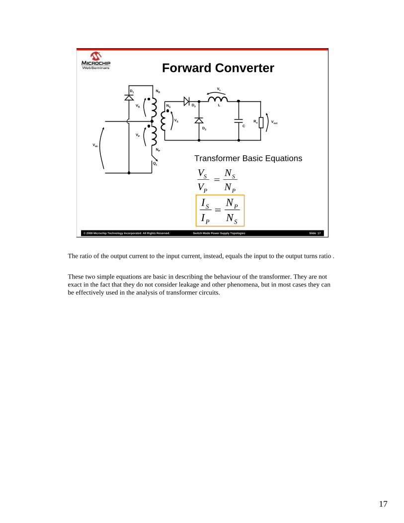
The ratio of the output current to the input current, instead, equals the input to the output turns ratio .
These two simple equations are basic in describing the behaviour of the transformer. They are not exact in the fact that they do not consider leakage and other phenomena, but in most cases they can be effectively used in the analysis of transformer circuits.

18
© 2008 Microchip Technology Incorporated. All Rights Reserved. Switch Mode Power Supply Topologies Slide 18
Forward ConverterLo
Co
Ro
Vout
VP
VR
VS
Q1
VL
Vdc
Q1Q1cmdcmd
TON TOFF
The analysis of the forward converter, because of the presence of the transformer, must be split, considering first what happens at the primary side and then the behaviour of the output circuuit. This approach is therefore a little bit more complex than the case of a buck converter.Moreover, we will see that, because of the specificity of the converter operation, time TOFF must be divided into two sub-intervals to get a full understanding of the circuit behavior.
19
© 2008 Microchip Technology Incorporated. All Rights Reserved. Switch Mode Power Supply Topologies Slide 19
Forward ConverterLo
Co
Ro
Vout
VP
VR
VS
Q1
VL
Vdc
Q1Q1cmdcmd
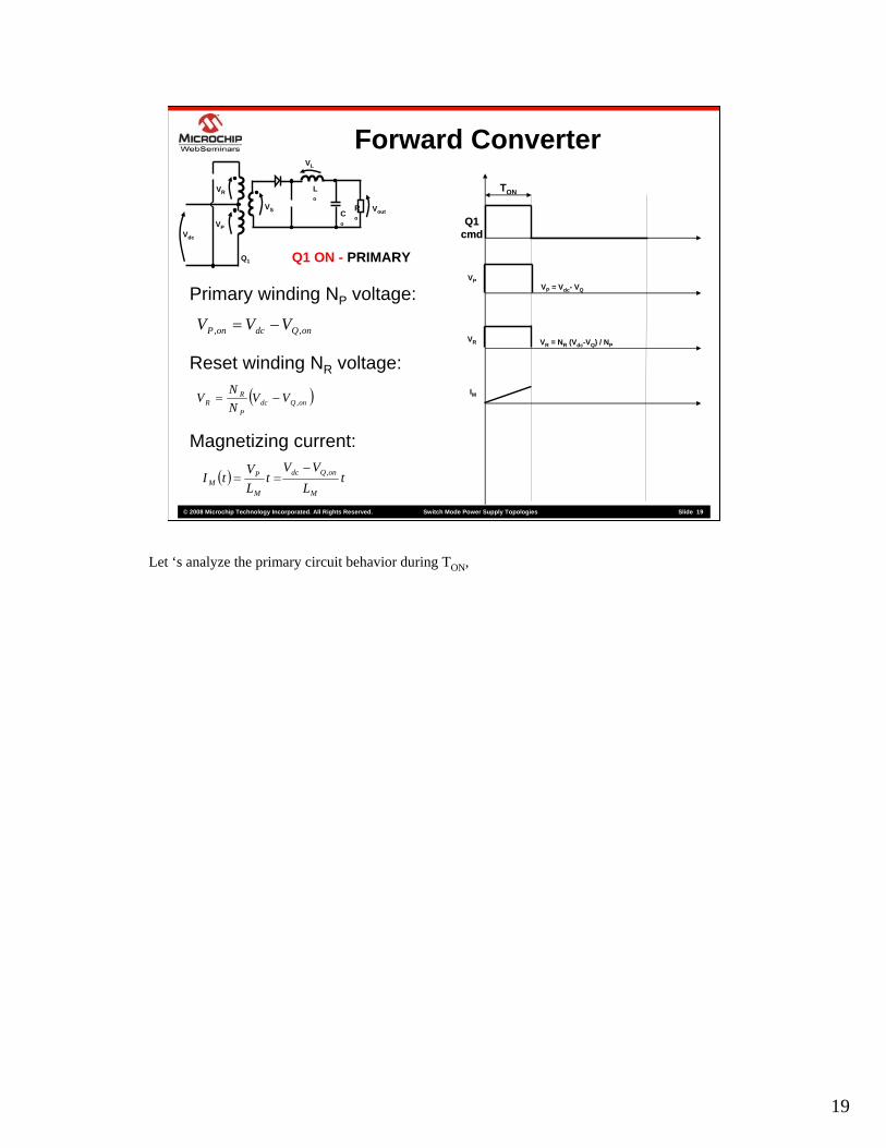
TON
onQdconP VVV ,, −=
VP = Vdc- VQPrimary winding NP voltage:
Reset winding NR voltage:
( )onQdcP
RR VV
NNV ,−=
VR = NR (Vdc-VQ) / NP
IM
Magnetizing current:
( ) tL
VVt
LV
tIM
onQdc
M
PM
,−==
Q1 ON - PRIMARYVP
VR
Let ‘s analyze the primary circuit behavior during TON,
20
© 2008 Microchip Technology Incorporated. All Rights Reserved. Switch Mode Power Supply Topologies Slide 20
Forward ConverterLo
Co
Ro
Vout
VP
VR
VS
Q1
VL
Vdc
Q1Q1cmdcmd
TON
onQdconP VVV ,, −=
VP = Vdc- VQPrimary winding NP voltage:
Reset winding NR voltage:
( )onQdcP
RR VV
NNV ,−=
VR = NR (Vdc-VQ) / NP
IM
Magnetizing current:
( ) tL
VVt
LV
tIM
onQdc
M
PM
,−==
Q1 ON - PRIMARYVP
VR
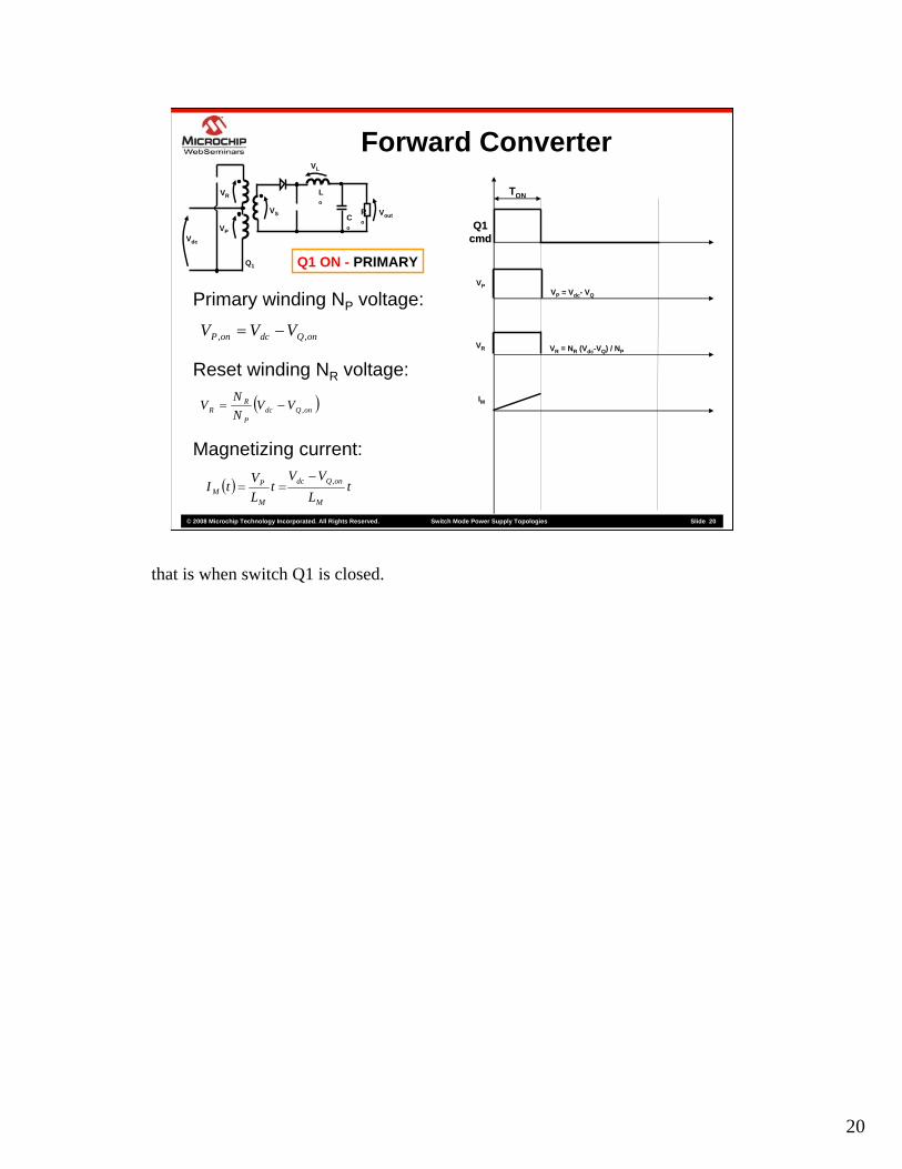
that is when switch Q1 is closed.
21
© 2008 Microchip Technology Incorporated. All Rights Reserved. Switch Mode Power Supply Topologies Slide 21
Forward ConverterLo
Co
Ro
Vout
VP
VR
VS
Q1
VL
Vdc
Q1Q1cmdcmd
TON
onQdconP VVV ,, −=
VP = Vdc- VQPrimary winding NP voltage:
Reset winding NR voltage:
( )onQdcP
RR VV
NNV ,−=
VR = NR (Vdc-VQ) / NP
IM
Magnetizing current:
( ) tL
VVt
LV
tIM
onQdc
M
PM
,−==
Q1 ON - PRIMARYVP
VR
+_
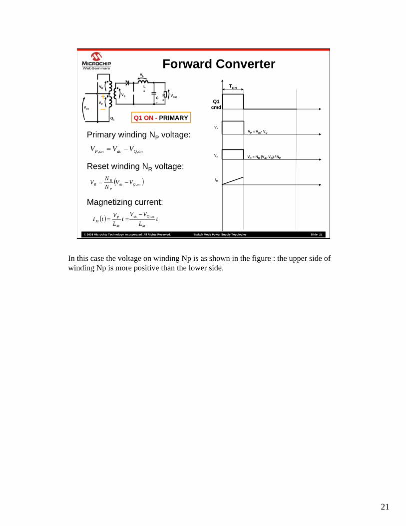
In this case the voltage on winding Np is as shown in the figure : the upper side of winding Np is more positive than the lower side.
22
© 2008 Microchip Technology Incorporated. All Rights Reserved. Switch Mode Power Supply Topologies Slide 22
Forward ConverterLo
Co
Ro
Vout
VP
VR
VS
Q1
VL
Vdc
Q1Q1cmdcmd
TON
onQdconP VVV ,, −=
VP = Vdc- VQPrimary winding NP voltage:
Reset winding NR voltage:
( )onQdcP
RR VV
NNV ,−=
VR = NR (Vdc-VQ) / NP
IM
Magnetizing current:
( ) tL
VVt
LV
tIM
onQdc
M
PM
,−==
Q1 ON - PRIMARYVP
VR
+_
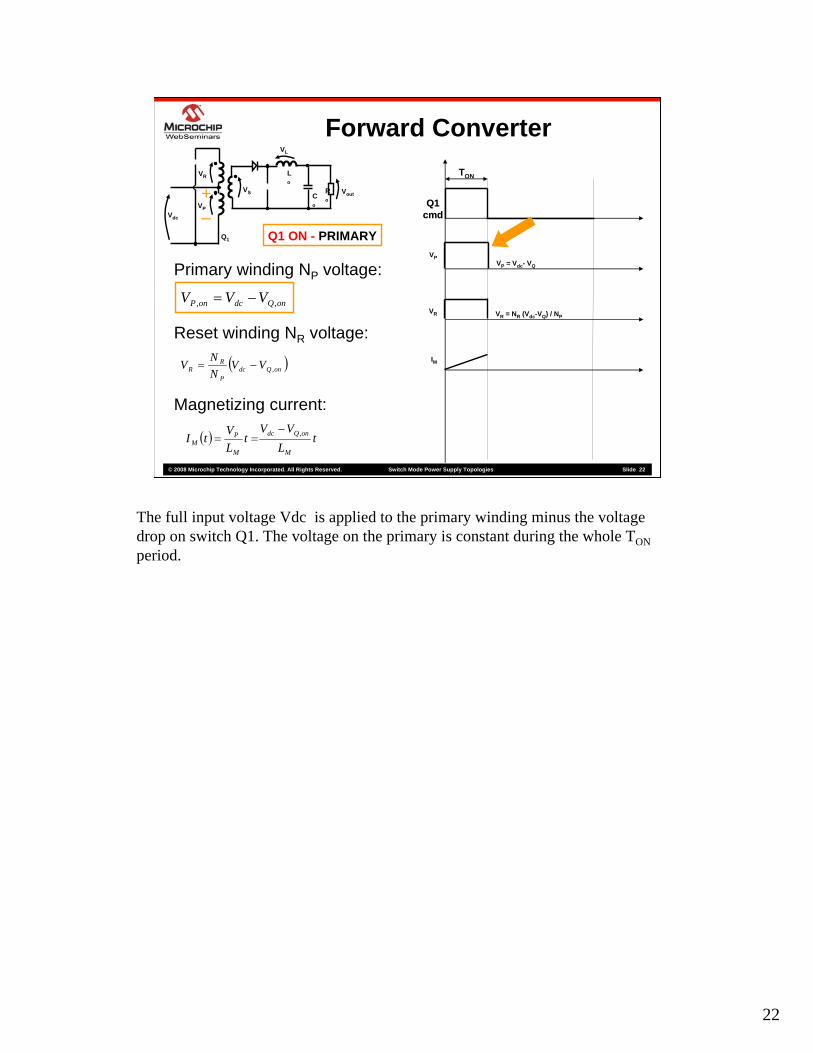
The full input voltage Vdc is applied to the primary winding minus the voltage drop on switch Q1. The voltage on the primary is constant during the whole TONperiod.

23
© 2008 Microchip Technology Incorporated. All Rights Reserved. Switch Mode Power Supply Topologies Slide 23
Forward ConverterLo
Co
Ro
Vout
VP
VR
VS
Q1
VL
Vdc
Q1Q1cmdcmd
TON
onQdconP VVV ,, −=
VP = Vdc- VQPrimary winding NP voltage:
Reset winding NR voltage:
( )onQdcP
RR VV
NNV ,−=
VR = NR (Vdc-VQ) / NP
IM
Magnetizing current:
( ) tL
VVt
LV
tIM
onQdc
M
PM
,−==
Q1 ON - PRIMARYVP
VR
+_
As a consequence diode D2 is reverse biased and can be removed from the circuit analysis; no current flows in the upper (reset) winding of the transformer.
24
© 2008 Microchip Technology Incorporated. All Rights Reserved. Switch Mode Power Supply Topologies Slide 24
Forward ConverterLo
Co
Ro
Vout
VP
VR
VS
Q1
VL
Vdc
Q1Q1cmdcmd
TON
onQdconP VVV ,, −=
VP = Vdc- VQPrimary winding NP voltage:
Reset winding NR voltage:
( )onQdcP
RR VV
NNV ,−=
VR = NR (Vdc-VQ) / NP
IM
Magnetizing current:
( ) tL
VVt
LV
tIM
onQdc
M
PM
,−==
Q1 ON - PRIMARYVP
VR
+_
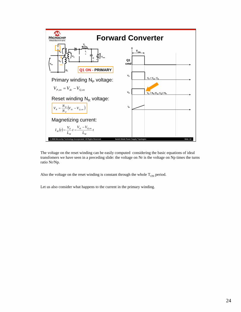
The voltage on the reset winding can be easily computed considering the basic equations of ideal transfomers we have seen in a preceding slide: the voltage on Nr is the voltage on Np times the turns ratio Nr/Np.
Also the voltage on the reset winding is constant through the whole TON period.
Let us also consider what happens to the current in the primary winding.
25
© 2008 Microchip Technology Incorporated. All Rights Reserved. Switch Mode Power Supply Topologies Slide 25
Forward ConverterLo
Co
Ro
Vout
VP
VR
VS
Q1
VL
Vdc
Q1Q1cmdcmd
TON
onQdconP VVV ,, −=
VP = Vdc- VQPrimary winding NP voltage:
Reset winding NR voltage:
( )onQdcP
RR VV
NNV ,−=
VR = NR (Vdc-VQ) / NP
IM
Magnetizing current:
( ) tL
VVt
LV
tIM
onQdc
M
PM
,−==
Q1 ON - PRIMARYVP
VR
+_
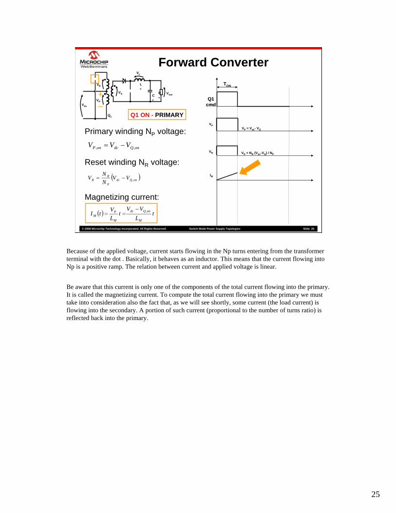
Because of the applied voltage, current starts flowing in the Np turns entering from the transformer terminal with the dot . Basically, it behaves as an inductor. This means that the current flowing into Np is a positive ramp. The relation between current and applied voltage is linear.
Be aware that this current is only one of the components of the total current flowing into the primary. It is called the magnetizing current. To compute the total current flowing into the primary we must take into consideration also the fact that, as we will see shortly, some current (the load current) is flowing into the secondary. A portion of such current (proportional to the number of turns ratio) is reflected back into the primary.

26
© 2008 Microchip Technology Incorporated. All Rights Reserved. Switch Mode Power Supply Topologies Slide 26
Forward Converter
Q1Q1cmdcmd
TON TOFF
Secondary winding voltage:
( )onQdcP
SS VV
NN
V ,−=VL
Output inductor voltage:( ) outonDonQdc
P
SL VVVV
NN
V −−−= ,,
IL
Output inductor current:( ) ( ) t
LV
iti LLL += 0
Lo
Co
Ro
Vout
VP
VR
VS
Q1
VL
Vdc
L
VS VS = NS (Vdc-VQ) / NP
Q1 ON - SECONDARY
Let us now analyze what happens at the secondary,
27
© 2008 Microchip Technology Incorporated. All Rights Reserved. Switch Mode Power Supply Topologies Slide 27
Forward Converter
Q1Q1cmdcmd
TON TOFF
Secondary winding voltage:
( )onQdcP
SS VV
NN
V ,−=VL
Output inductor voltage:( ) outonDonQdc
P
SL VVVV
NN
V −−−= ,,
IL
Output inductor current:( ) ( ) t
LV
iti LLL += 0
Lo
Co
Ro
Vout
VP
VR
VS
Q1
VL
Vdc
L
VS VS = NS (Vdc-VQ) / NP
Q1 ON - SECONDARY
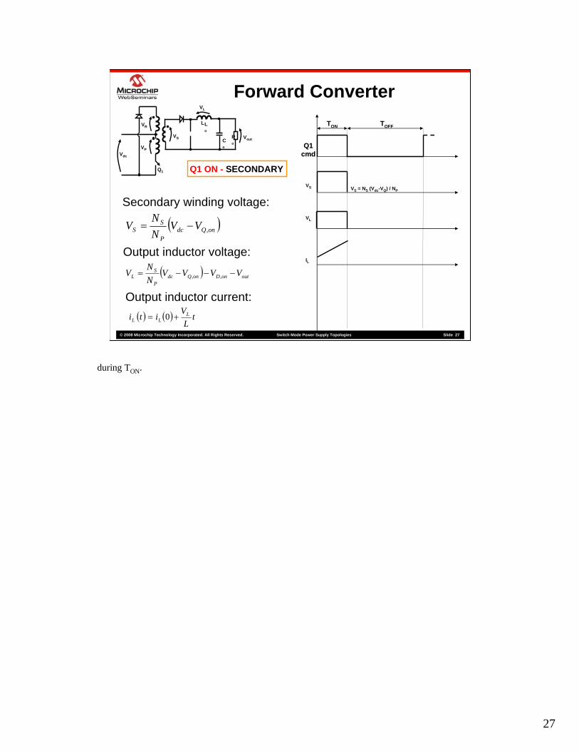
during TON.

28
© 2008 Microchip Technology Incorporated. All Rights Reserved. Switch Mode Power Supply Topologies Slide 28
Forward Converter
Q1Q1cmdcmd
TON TOFF
Secondary winding voltage:
( )onQdcP
SS VV
NN
V ,−=VL
Output inductor voltage:( ) outonDonQdc
P
SL VVVV
NN
V −−−= ,,
IL
Output inductor current:( ) ( ) t
LV
iti LLL += 0
Lo
Co
Ro
Vout
VP
VR
VS
Q1
VL
Vdc
L
VS VS = NS (Vdc-VQ) / NP
Q1 ON - SECONDARY
+_
The upper edge of the secondary winding is more positive (because of the voltage on the primary) than the lower edge,

29
© 2008 Microchip Technology Incorporated. All Rights Reserved. Switch Mode Power Supply Topologies Slide 29
Forward Converter
Q1Q1cmdcmd
TON TOFF
Secondary winding voltage:
( )onQdcP
SS VV
NN
V ,−=VL
Output inductor voltage:( ) outonDonQdc
P
SL VVVV
NN
V −−−= ,,
IL
Output inductor current:( ) ( ) t
LV
iti LLL += 0
Lo
Co
Ro
Vout
VP
VR
VS
Q1
VL
Vdc
L
VS VS = NS (Vdc-VQ) / NP
Q1 ON - SECONDARY
+_
consequently diode D2 is forward biased and D3 is reverse biased (open circuit) .
30
© 2008 Microchip Technology Incorporated. All Rights Reserved. Switch Mode Power Supply Topologies Slide 30
Forward Converter
Q1Q1cmdcmd
TON TOFF
Secondary winding voltage:
( )onQdcP
SS VV
NN
V ,−=VL
Output inductor voltage:( ) outonDonQdc
P
SL VVVV
NN
V −−−= ,,
IL
Output inductor current:( ) ( ) t
LV
iti LLL += 0
Lo
Co
Ro
Vout
VP
VR
VS
Q1
VL
Vdc
L
VS VS = NS (Vdc-VQ) / NP
Q1 ON - SECONDARY
+_
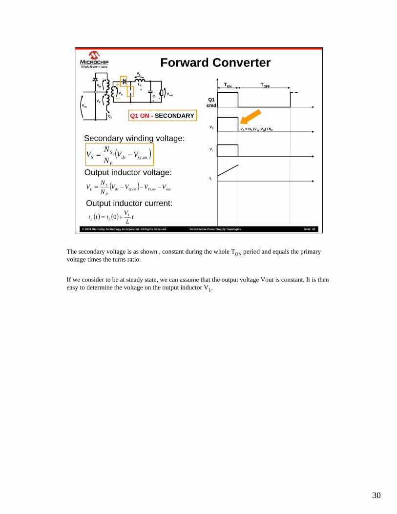
The secondary voltage is as shown , constant during the whole TON period and equals the primary voltage times the turns ratio.
If we consider to be at steady state, we can assume that the output voltage Vout is constant. It is then easy to determine the voltage on the output inductor VL.
31
© 2008 Microchip Technology Incorporated. All Rights Reserved. Switch Mode Power Supply Topologies Slide 31
Forward Converter
Q1Q1cmdcmd
TON TOFF
Secondary winding voltage:
( )onQdcP
SS VV
NN
V ,−=VL
Output inductor voltage:( ) outonDonQdc
P
SL VVVV
NN
V −−−= ,,
IL
Output inductor current:( ) ( ) t
LV
iti LLL += 0
Lo
Co
Ro
Vout
VP
VR
VS
Q1
VL
Vdc
L
VS VS = NS (Vdc-VQ) / NP
+ -
Q1 ON - SECONDARY
+_
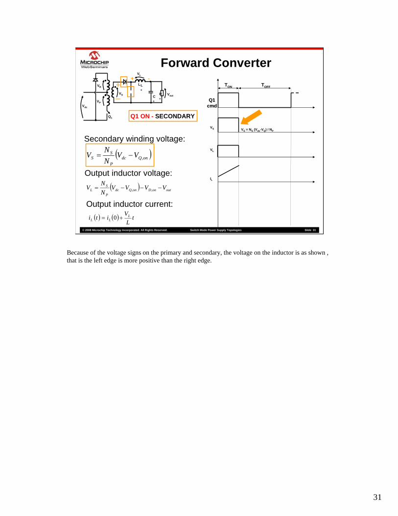
Because of the voltage signs on the primary and secondary, the voltage on the inductor is as shown , that is the left edge is more positive than the right edge.
32
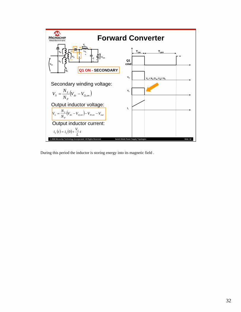
© 2008 Microchip Technology Incorporated. All Rights Reserved. Switch Mode Power Supply Topologies Slide 32
Forward Converter
Q1Q1cmdcmd
TON TOFF
Secondary winding voltage:
( )onQdcP
SS VV
NN
V ,−=VL
Output inductor voltage:( ) outonDonQdc
P
SL VVVV
NN
V −−−= ,,
IL
Output inductor current:( ) ( ) t
LV
iti LLL += 0
Lo
Co
Ro
Vout
VP
VR
VS
Q1
VL
Vdc
L
VS VS = NS (Vdc-VQ) / NP
+ -
Q1 ON - SECONDARY
+_
During this period the inductor is storing energy into its magnetic field .
33
© 2008 Microchip Technology Incorporated. All Rights Reserved. Switch Mode Power Supply Topologies Slide 33
Forward Converter
Q1Q1cmdcmd
TON TOFF
Secondary winding voltage:
( )onQdcP
SS VV
NN
V ,−=VL
Output inductor voltage:( ) outonDonQdc
P
SL VVVV
NN
V −−−= ,,
IL
Output inductor current:( ) ( ) t
LV
iti LLL += 0
Lo
Co
Ro
Vout
VP
VR
VS
Q1
VL
Vdc
L
VS VS = NS (Vdc-VQ) / NP
+ -
Q1 ON - SECONDARY
+_
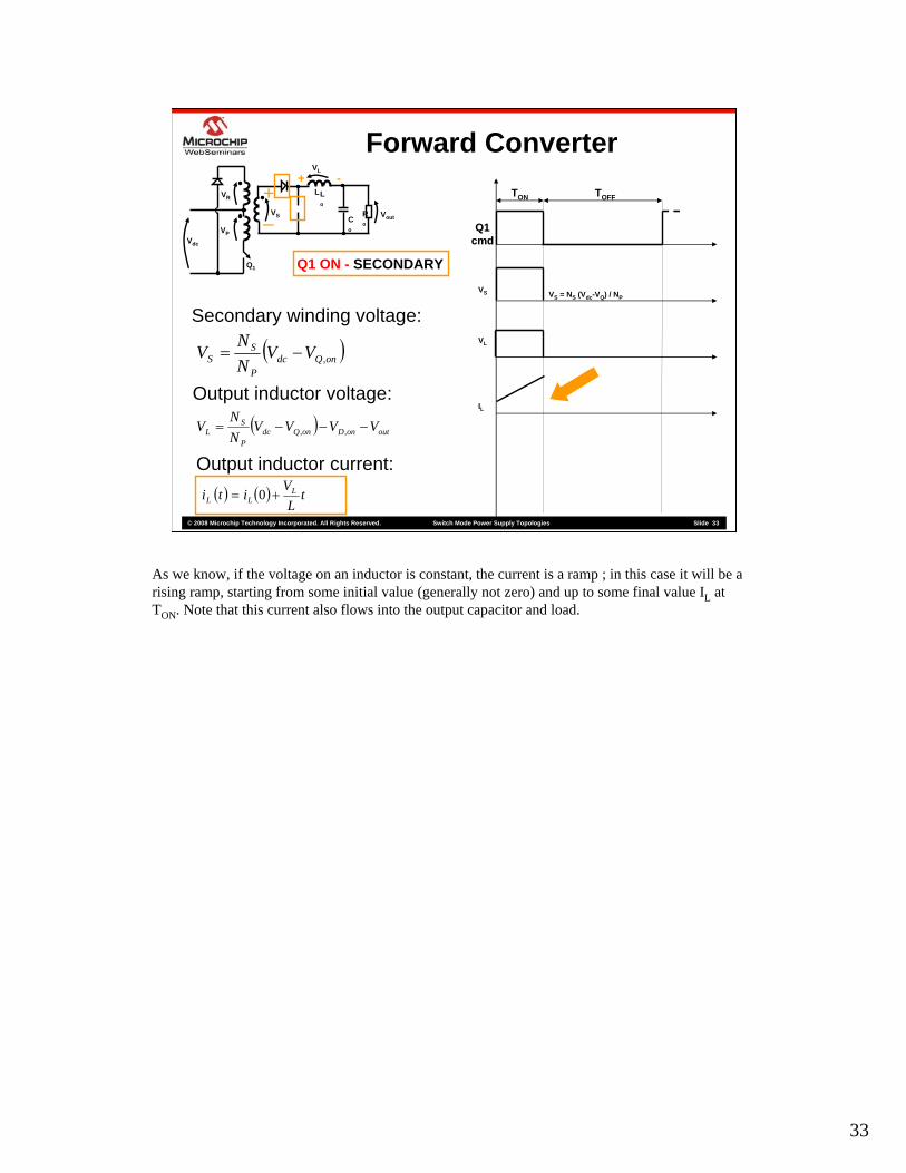
As we know, if the voltage on an inductor is constant, the current is a ramp ; in this case it will be a rising ramp, starting from some initial value (generally not zero) and up to some final value IL at TON. Note that this current also flows into the output capacitor and load.
34
© 2008 Microchip Technology Incorporated. All Rights Reserved. Switch Mode Power Supply Topologies Slide 34
Forward Converter
Q1Q1cmdcmd
TON TOFF
VL
IL
Lo
Co
Ro
Vout
VP
VR
VS
Q1
VL
Vdc
L
IP total
primary magnetizing current
output inductor reflected current
primary total current
Primary winding total current:
( ) ( )tINN
tIII LP
SMPtotalP ++= )(0,
VS
Q1 ON - PRIMARY
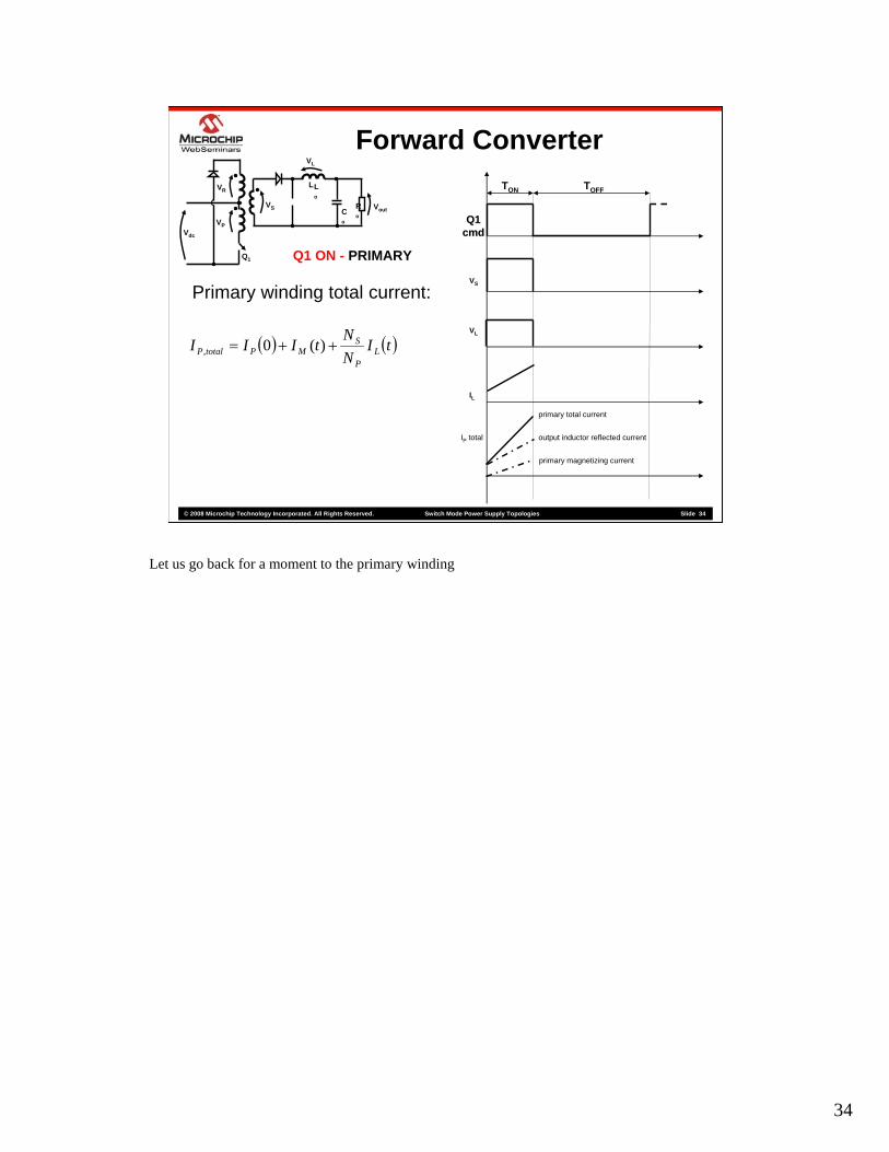
Let us go back for a moment to the primary winding
35
© 2008 Microchip Technology Incorporated. All Rights Reserved. Switch Mode Power Supply Topologies Slide 35
Forward Converter
Q1Q1cmdcmd
TON TOFF
VL
IL
Lo
Co
Ro
Vout
VP
VR
VS
Q1
VL
Vdc
L
IP total
primary magnetizing current
output inductor reflected current
primary total current
Primary winding total current:
( ) ( )tINN
tIII LP
SMPtotalP ++= )(0,
VS
Q1 ON - PRIMARY
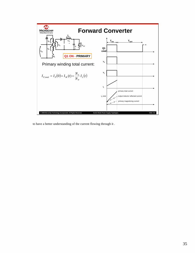
to have a better understanding of the current flowing through it .

36
© 2008 Microchip Technology Incorporated. All Rights Reserved. Switch Mode Power Supply Topologies Slide 36
Forward Converter
Q1Q1cmdcmd
TON TOFF
VL
IL
Lo
Co
Ro
Vout
VP
VR
VS
Q1
VL
Vdc
L
IP total
primary magnetizing current
output inductor reflected current
primary total current
Primary winding total current:
( ) ( )tINN
tIII LP
SMPtotalP ++= )(0,
VS
Q1 ON - PRIMARY
As we have seen in a previous slide, one component of the primary current is the magnetizing current , which is a ramp whose slope is directly proportional to the input voltage and inversely to the magnetizing inductance of the transformer.
37
© 2008 Microchip Technology Incorporated. All Rights Reserved. Switch Mode Power Supply Topologies Slide 37
Forward Converter
Q1Q1cmdcmd
TON TOFF
VL
IL
Lo
Co
Ro
Vout
VP
VR
VS
Q1
VL
Vdc
L
IP total
primary magnetizing current
output inductor reflected current
primary total current
Primary winding total current:
( ) ( )tINN
tIII LP
SMPtotalP ++= )(0,
VS
Q1 ON - PRIMARY
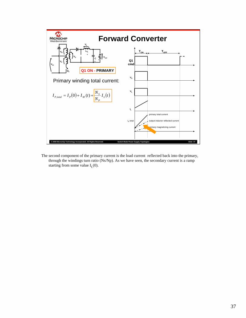
The second component of the primary current is the load current reflected back into the primary, through the windings turn ratio (Ns/Np). As we have seen, the secondary current is a ramp starting from some value IL(0).
38
© 2008 Microchip Technology Incorporated. All Rights Reserved. Switch Mode Power Supply Topologies Slide 38
Forward Converter
Q1Q1cmdcmd
TON TOFF
VL
IL
Lo
Co
Ro
Vout
VP
VR
VS
Q1
VL
Vdc
L
IP total
primary magnetizing current
output inductor reflected current
primary total current
Primary winding total current:
( ) ( )tINN
tIII LP
SMPtotalP ++= )(0,
VS
Q1 ON - PRIMARY
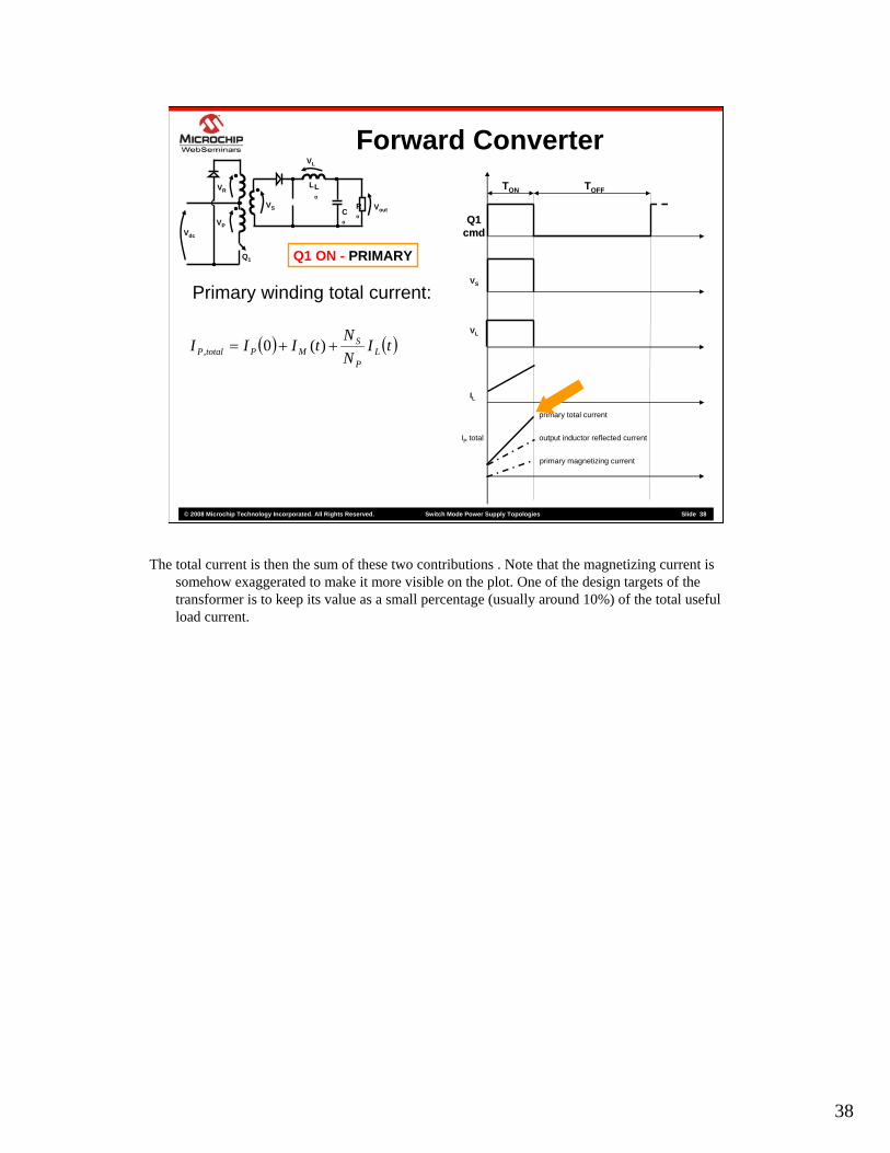
The total current is then the sum of these two contributions . Note that the magnetizing current is somehow exaggerated to make it more visible on the plot. One of the design targets of the transformer is to keep its value as a small percentage (usually around 10%) of the total useful load current.
39
© 2008 Microchip Technology Incorporated. All Rights Reserved. Switch Mode Power Supply Topologies Slide 39
Forward ConverterLo
Co
Ro
Vout
VP
VR
VS
Q1
VL
Vdc
Q1Q1cmdcmd
TOFF
Voltage on the reset winding:
( )onDdcR VVV ,+−=
VP
VR = - NP (Vdc+ VD,on) / NR
Voltage on the primary winding:
( )onDdcR
PP VV
NN
V ,+−=
VR
Reset winding current:
MR
PR I
NNI =
IM
Q1 OFF - PRIMARY
VR = - (Vdc+ VD,on)
TR
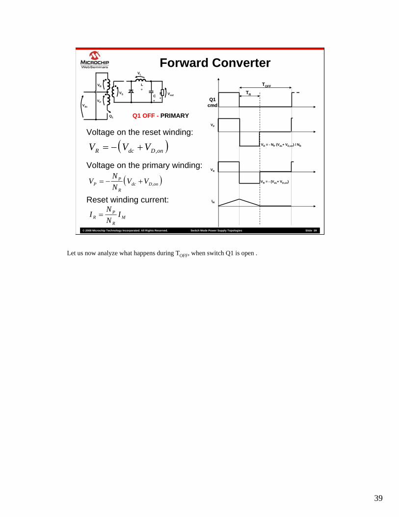
Let us now analyze what happens during TOFF, when switch Q1 is open .
40
© 2008 Microchip Technology Incorporated. All Rights Reserved. Switch Mode Power Supply Topologies Slide 40
Forward ConverterLo
Co
Ro
Vout
VP
VR
VS
Q1
VL
Vdc
Q1Q1cmdcmd
TOFF
Voltage on the reset winding:
( )onDdcR VVV ,+−=
VP
VR = - NP (Vdc+ VD,on) / NR
Voltage on the primary winding:
( )onDdcR
PP VV
NN
V ,+−=
VR
Reset winding current:
MR
PR I
NNI =
IM
Q1 OFF - PRIMARY
VR = - (Vdc+ VD,on)
TR
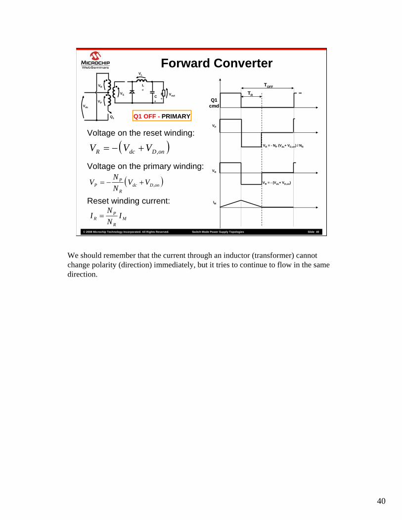
We should remember that the current through an inductor (transformer) cannot change polarity (direction) immediately, but it tries to continue to flow in the same direction.
41
© 2008 Microchip Technology Incorporated. All Rights Reserved. Switch Mode Power Supply Topologies Slide 41
Forward ConverterLo
Co
Ro
Vout
VP
VR
VS
Q1
VL
Vdc
Q1Q1cmdcmd
TOFF
Voltage on the reset winding:
( )onDdcR VVV ,+−=
VP
VR = - NP (Vdc+ VD,on) / NR
Voltage on the primary winding:
( )onDdcR
PP VV
NN
V ,+−=
VR
Reset winding current:
MR
PR I
NNI =
IM
Q1 OFF - PRIMARY
VR = - (Vdc+ VD,on)
TR
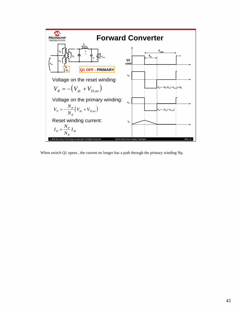
When switch Q1 opens , the current no longer has a path through the primary winding Np.
42
© 2008 Microchip Technology Incorporated. All Rights Reserved. Switch Mode Power Supply Topologies Slide 42
Forward ConverterLo
Co
Ro
Vout
VP
VR
VS
Q1
VL
Vdc
Q1Q1cmdcmd
TOFF
Voltage on the reset winding:
( )onDdcR VVV ,+−=
VP
VR = - NP (Vdc+ VD,on) / NR
Voltage on the primary winding:
( )onDdcR
PP VV
NN
V ,+−=
VR
Reset winding current:
MR
PR I
NNI =
IM
Q1 OFF - PRIMARY
_
+
VR = - (Vdc+ VD,on)
TR
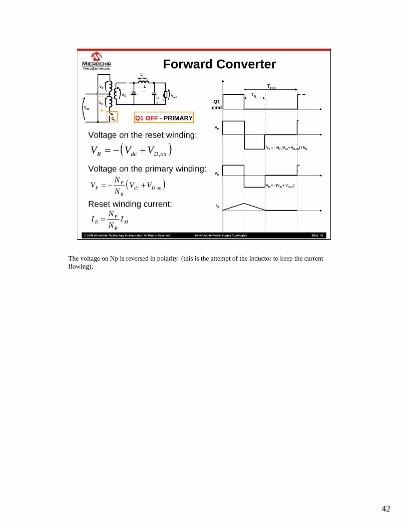
The voltage on Np is reversed in polarity (this is the attempt of the inductor to keep the current flowing),
43
© 2008 Microchip Technology Incorporated. All Rights Reserved. Switch Mode Power Supply Topologies Slide 43
Forward ConverterLo
Co
Ro
Vout
VP
VR
VS
Q1
VL
Vdc
Q1Q1cmdcmd
TOFF
Voltage on the reset winding:
( )onDdcR VVV ,+−=
VP
VR = - NP (Vdc+ VD,on) / NR
Voltage on the primary winding:
( )onDdcR
PP VV
NN
V ,+−=
VR
Reset winding current:
MR
PR I
NNI =
IM
Q1 OFF - PRIMARY
_
+
_
+
VR = - (Vdc+ VD,on)
TR
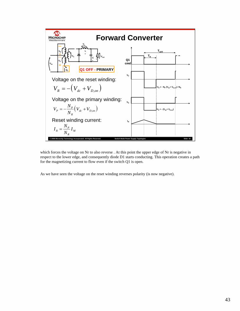
which forces the voltage on Nr to also reverse . At this point the upper edge of Nr is negative in respect to the lower edge, and consequently diode D1 starts conducting. This operation creates a path for the magnetizing current to flow even if the switch Q1 is open.
As we have seen the voltage on the reset winding reverses polarity (is now negative).
44
© 2008 Microchip Technology Incorporated. All Rights Reserved. Switch Mode Power Supply Topologies Slide 44
Forward ConverterLo
Co
Ro
Vout
VP
VR
VS
Q1
VL
Vdc
Q1Q1cmdcmd
TOFF
Voltage on the reset winding:
( )onDdcR VVV ,+−=
VP
VR = - NP (Vdc+ VD,on) / NR
Voltage on the primary winding:
( )onDdcR
PP VV
NN
V ,+−=
VR
Reset winding current:
MR
PR I
NNI =
IM
Q1 OFF - PRIMARY
_
+
_
+
VR = - (Vdc+ VD,on)
TR
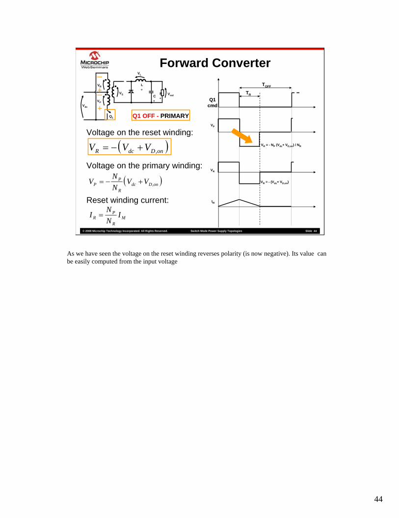
As we have seen the voltage on the reset winding reverses polarity (is now negative). Its value can be easily computed from the input voltage

45
© 2008 Microchip Technology Incorporated. All Rights Reserved. Switch Mode Power Supply Topologies Slide 45
Forward ConverterLo
Co
Ro
Vout
VP
VR
VS
Q1
VL
Vdc
Q1Q1cmdcmd
TOFF
Voltage on the reset winding:
( )onDdcR VVV ,+−=
VP
VR = - NP (Vdc+ VD,on) / NR
Voltage on the primary winding:
( )onDdcR
PP VV
NN
V ,+−=
VR
Reset winding current:
MR
PR I
NNI =
IM
Q1 OFF - PRIMARY
_
+
_
+
VR = - (Vdc+ VD,on)
TR
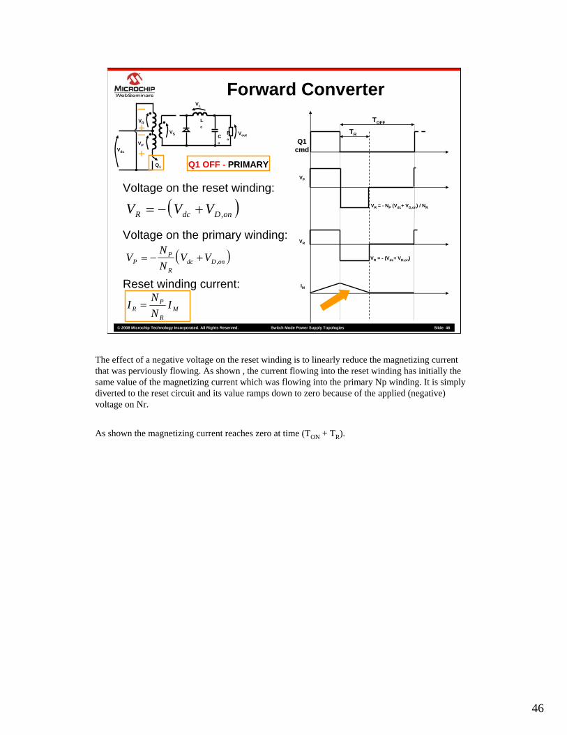
The voltage on the primary can then be otained from the reset voltage multiplied by the Nr/Np transformer turns ratio.The effect of a negative voltage on the reset winding is to linearly reduce the magnetizing current that was perviously flowing.
46
© 2008 Microchip Technology Incorporated. All Rights Reserved. Switch Mode Power Supply Topologies Slide 46
Forward ConverterLo
Co
Ro
Vout
VP
VR
VS
Q1
VL
Vdc
Q1Q1cmdcmd
TOFF
Voltage on the reset winding:
( )onDdcR VVV ,+−=
VP
VR = - NP (Vdc+ VD,on) / NR
Voltage on the primary winding:
( )onDdcR
PP VV
NN
V ,+−=
VR
Reset winding current:
MR
PR I
NNI =
IM
Q1 OFF - PRIMARY
_
+
_
+
VR = - (Vdc+ VD,on)
TR
The effect of a negative voltage on the reset winding is to linearly reduce the magnetizing current that was perviously flowing. As shown , the current flowing into the reset winding has initially the same value of the magnetizing current which was flowing into the primary Np winding. It is simply diverted to the reset circuit and its value ramps down to zero because of the applied (negative) voltage on Nr.
As shown the magnetizing current reaches zero at time (TON + TR).

47
© 2008 Microchip Technology Incorporated. All Rights Reserved. Switch Mode Power Supply Topologies Slide 47
Forward ConverterLo
Co
Ro
Vout
VP
VR
VS
Q1
VL
Vdc
Q1Q1cmdcmd
TOFF
Voltage on the reset winding:
( )onDdcR VVV ,+−=
VP
VR = - NP (Vdc+ VD,on) / NR
Voltage on the primary winding:
( )onDdcR
PP VV
NN
V ,+−=
VR
Reset winding current:
MR
PR I
NNI =
IM
Q1 OFF - PRIMARY
_
+
_
+
VR = - (Vdc+ VD,on)
TR
In this presentation we suppose that TOFF is longer than TR, so that the primary winding is completely de enegized before the next pwm cycle.
48
© 2008 Microchip Technology Incorporated. All Rights Reserved. Switch Mode Power Supply Topologies Slide 48
Forward ConverterLo
Co
Ro
Vout
VP
VR
VS
Q1
VL
Vdc
Q1Q1cmdcmd
TOFF
Output inductor voltage:
onDoutL VVV ,−−=
Output inductor current:
( ) ( ) tLVV
TItI onDoutONL
,+−=
VL
IL
TR
Q1 OFF - SECONDARY
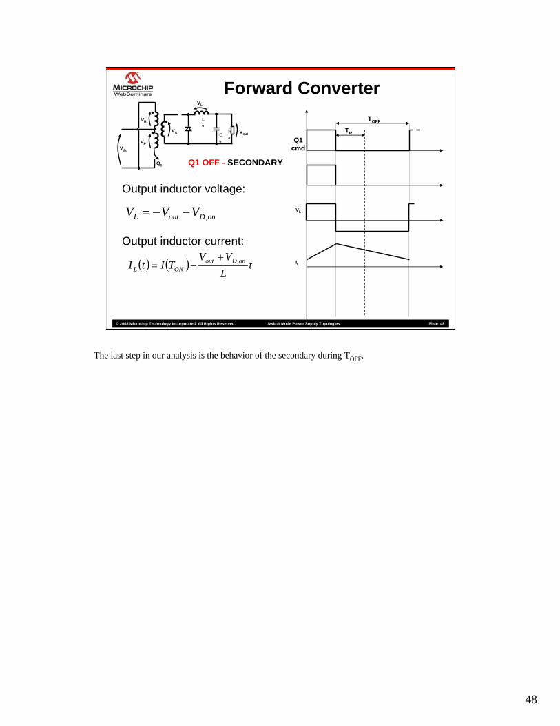
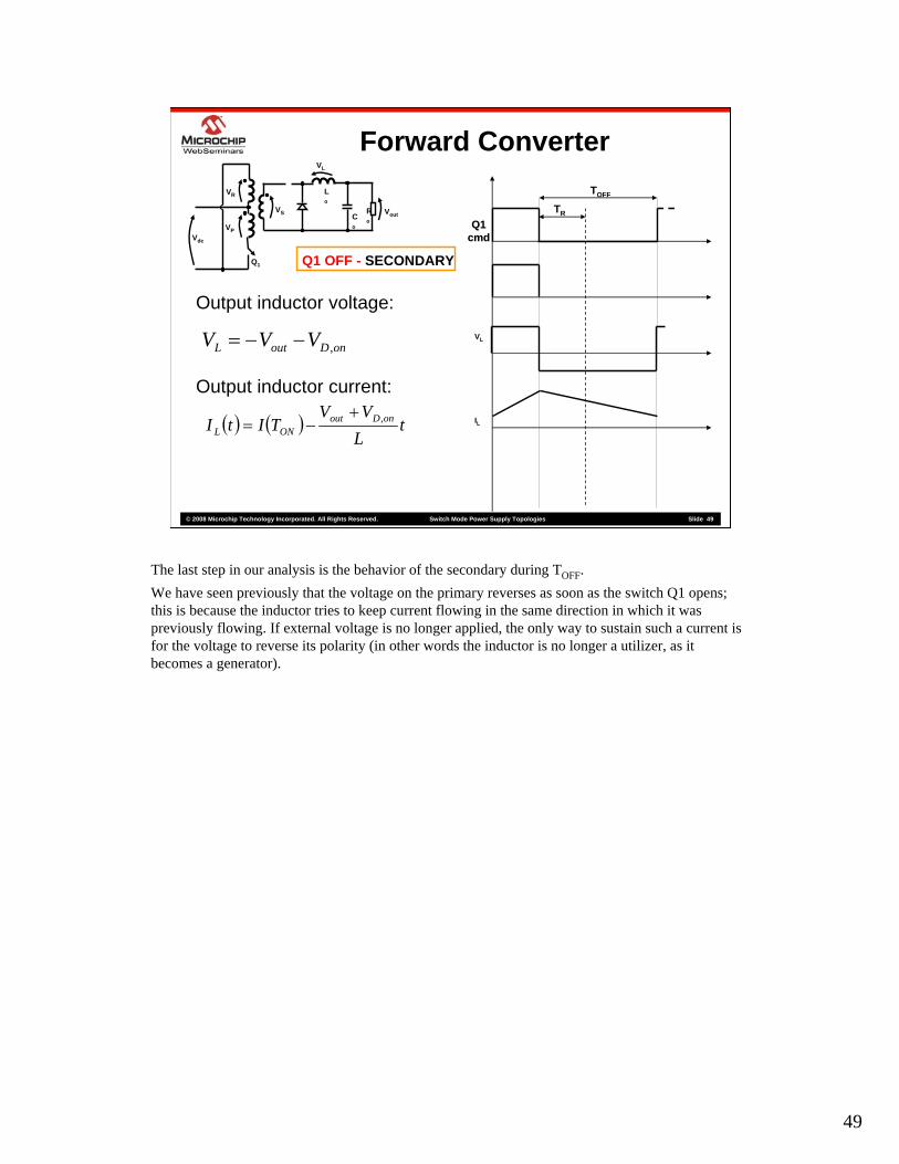
The last step in our analysis is the behavior of the secondary during TOFF.
49
© 2008 Microchip Technology Incorporated. All Rights Reserved. Switch Mode Power Supply Topologies Slide 49
Forward ConverterLo
Co
Ro
Vout
VP
VR
VS
Q1
VL
Vdc
Q1Q1cmdcmd
TOFF
Output inductor voltage:
onDoutL VVV ,−−=
Output inductor current:
( ) ( ) tLVV
TItI onDoutONL
,+−=
VL
IL
TR
Q1 OFF - SECONDARY
The last step in our analysis is the behavior of the secondary during TOFF. We have seen previously that the voltage on the primary reverses as soon as the switch Q1 opens; this is because the inductor tries to keep current flowing in the same direction in which it was previously flowing. If external voltage is no longer applied, the only way to sustain such a current is for the voltage to reverse its polarity (in other words the inductor is no longer a utilizer, as it becomes a generator).
50
© 2008 Microchip Technology Incorporated. All Rights Reserved. Switch Mode Power Supply Topologies Slide 50
Forward ConverterLo
Co
Ro
Vout
VP
VR
VS
Q1
VL
Vdc
Q1Q1cmdcmd
TOFF
Output inductor voltage:
onDoutL VVV ,−−=
Output inductor current:
( ) ( ) tLVV
TItI onDoutONL
,+−=
VL
IL
TR
Q1 OFF - SECONDARY
_
+
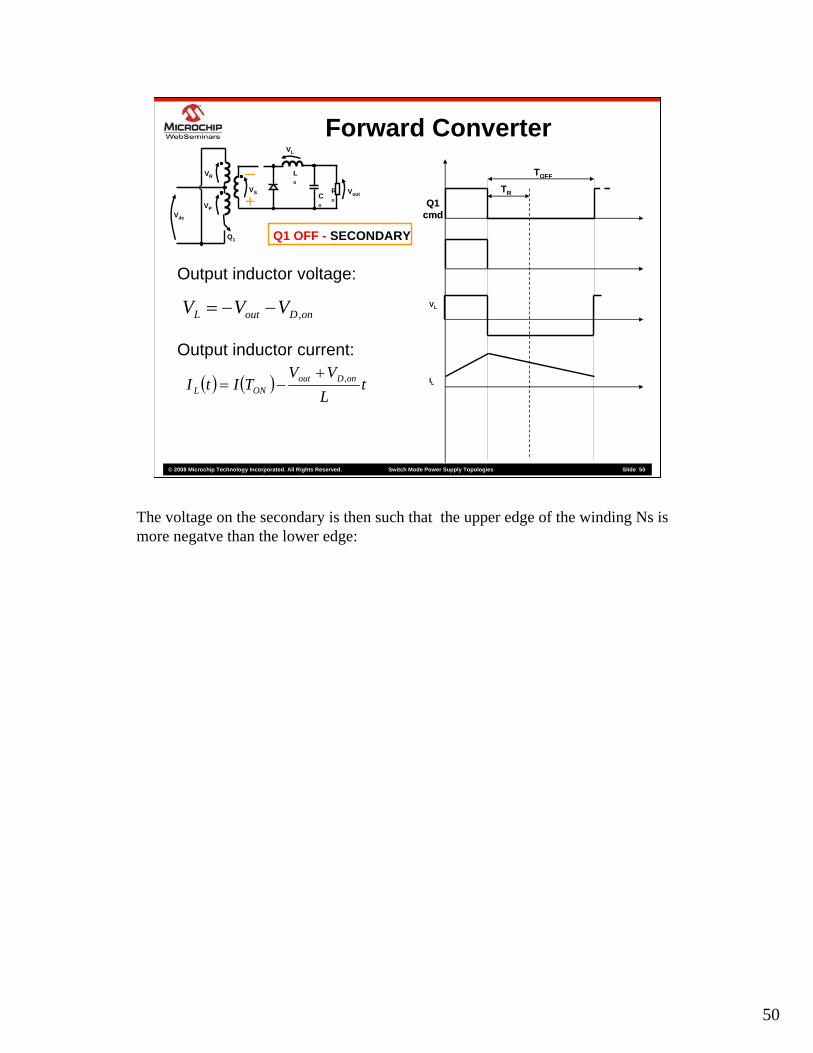
The voltage on the secondary is then such that the upper edge of the winding Ns is more negatve than the lower edge:
51
© 2008 Microchip Technology Incorporated. All Rights Reserved. Switch Mode Power Supply Topologies Slide 51
Forward ConverterLo
Co
Ro
Vout
VP
VR
VS
Q1
VL
Vdc
Q1Q1cmdcmd
TOFF
Output inductor voltage:
onDoutL VVV ,−−=
Output inductor current:
( ) ( ) tLVV
TItI onDoutONL
,+−=
VL
IL
TR
Q1 OFF - SECONDARY
_
+
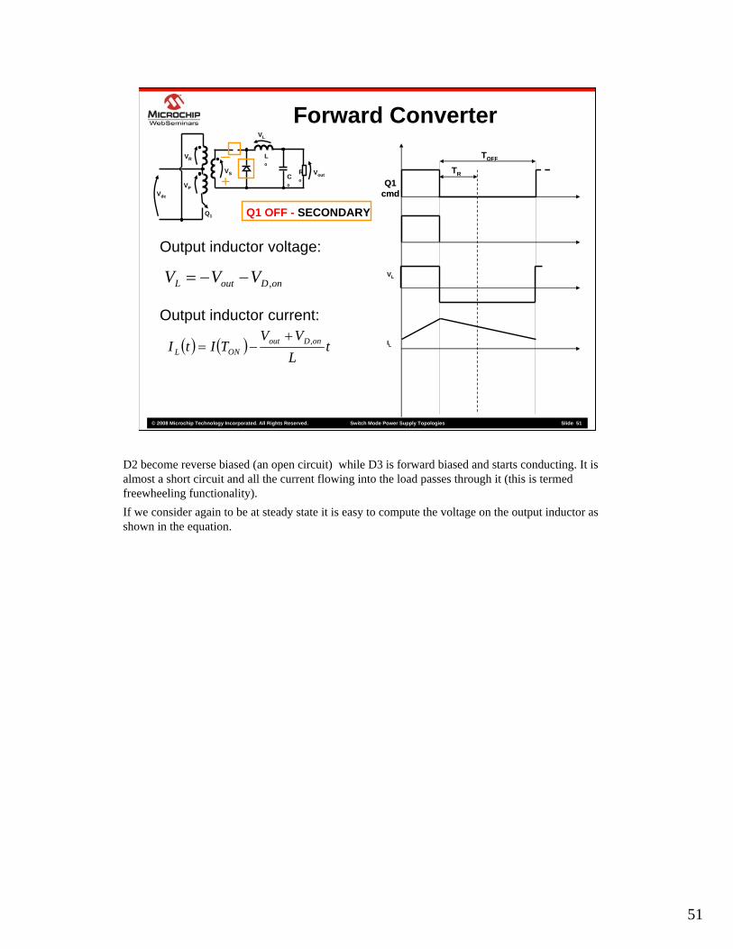
D2 become reverse biased (an open circuit) while D3 is forward biased and starts conducting. It is almost a short circuit and all the current flowing into the load passes through it (this is termed freewheeling functionality).If we consider again to be at steady state it is easy to compute the voltage on the output inductor as shown in the equation.
52
© 2008 Microchip Technology Incorporated. All Rights Reserved. Switch Mode Power Supply Topologies Slide 52
Forward ConverterLo
Co
Ro
Vout
VP
VR
VS
Q1
VL
Vdc
Q1Q1cmdcmd
TOFF
Output inductor voltage:
onDoutL VVV ,−−=
Output inductor current:
( ) ( ) tLVV
TItI onDoutONL
,+−=
VL
IL
TR
Q1 OFF - SECONDARY
_
+
- +
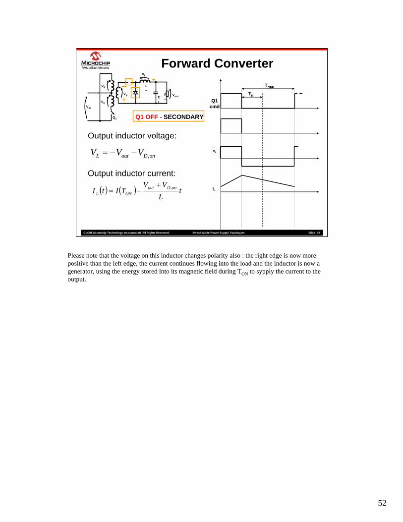
Please note that the voltage on this inductor changes polarity also : the right edge is now more positive than the left edge, the current continues flowing into the load and the inductor is now a generator, using the energy stored into its magnetic field during TON to sypply the current to the output.
53
© 2008 Microchip Technology Incorporated. All Rights Reserved. Switch Mode Power Supply Topologies Slide 53
Forward ConverterLo
Co
Ro
Vout
VP
VR
VS
Q1
VL
Vdc
Q1Q1cmdcmd
TOFF
Output inductor voltage:
onDoutL VVV ,−−=
Output inductor current:
( ) ( ) tLVV
TItI onDoutONL
,+−=
VL
IL
TR
Q1 OFF - SECONDARY
_
+
- +
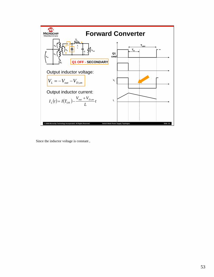
Since the inductor voltage is constant ,
54
© 2008 Microchip Technology Incorporated. All Rights Reserved. Switch Mode Power Supply Topologies Slide 54
Forward ConverterLo
Co
Ro
Vout
VP
VR
VS
Q1
VL
Vdc
Q1Q1cmdcmd
TOFF
Output inductor voltage:
onDoutL VVV ,−−=
Output inductor current:
( ) ( ) tLVV
TItI onDoutONL
,+−=
VL
IL
TR
Q1 OFF - SECONDARY
_
+
- +
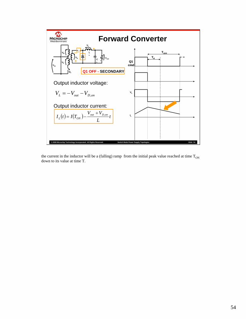
the current in the inductor will be a (falling) ramp from the initial peak value reached at time TONdown to its value at time T.
55
© 2008 Microchip Technology Incorporated. All Rights Reserved. Switch Mode Power Supply Topologies Slide 55
Forward ConverterLo
Co
Ro
Vout
VP
VR
VS
Q1
VL
Vdc
Q1Q1cmdcmd
TOFF
Output inductor voltage:
onDoutL VVV ,−−=
Output inductor current:
( ) ( ) tLVV
TItI onDoutONL
,+−=
VL
IL
TR
Q1 OFF - SECONDARY
_
+
- +
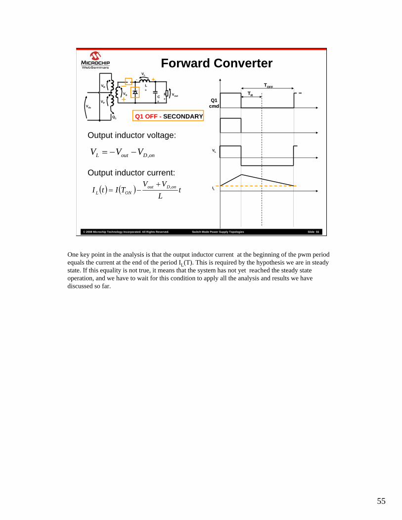
One key point in the analysis is that the output inductor current at the beginning of the pwm period equals the current at the end of the period IL(T). This is required by the hypothesis we are in steady state. If this equality is not true, it means that the system has not yet reached the steady state operation, and we have to wait for this condition to apply all the analysis and results we have discussed so far.
56
© 2008 Microchip Technology Incorporated. All Rights Reserved. Switch Mode Power Supply Topologies Slide 56
Forward ConverterLo
Co
Ro
Vout
VP
VR
VS
Q1
VL
Vdc
Q1Q1cmdcmd
TTON + TR
Q1 OFF VP
VR
VL
IL
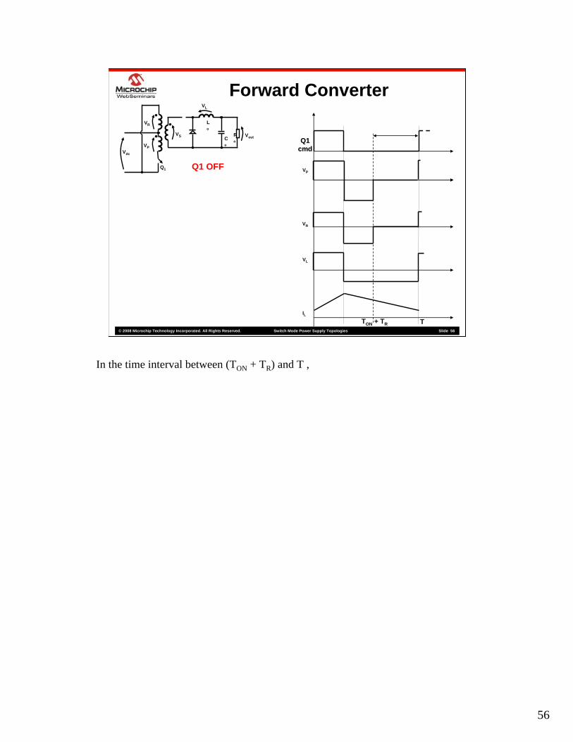
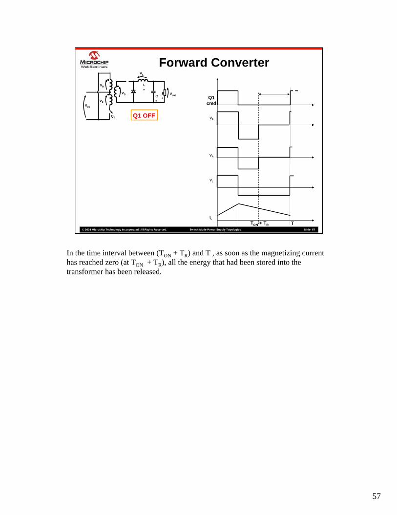
In the time interval between (TON + TR) and T ,
57
© 2008 Microchip Technology Incorporated. All Rights Reserved. Switch Mode Power Supply Topologies Slide 57
Forward ConverterLo
Co
Ro
Vout
VP
VR
VS
Q1
VL
Vdc
Q1Q1cmdcmd
TTON + TR
Q1 OFF VP
VR
VL
IL
In the time interval between (TON + TR) and T , as soon as the magnetizing current has reached zero (at TON + TR), all the energy that had been stored into the transformer has been released.

58
© 2008 Microchip Technology Incorporated. All Rights Reserved. Switch Mode Power Supply Topologies Slide 58
Forward ConverterLo
Co
Ro
Vout
VP
VR
VS
Q1
VL
Vdc
Q1Q1cmdcmd
TTON + TR
Q1 OFF VP
VR
VL
IL
The voltage drop on NR becomes zero and the voltages at both ends of NR equal Vdc. Diode D1 becomes reverse biased and is no longer conducting.

59
© 2008 Microchip Technology Incorporated. All Rights Reserved. Switch Mode Power Supply Topologies Slide 59
Forward ConverterLo
Co
Ro
Vout
VP
VR
VS
Q1
VL
Vdc
Q1Q1cmdcmd
TTON + TR
Q1 OFF VP
VR
VL
IL
The voltage drop on NP becomes zero .
As for the output circuit, nothing changes compared to the time interval from TON to (TON + TR).
60
© 2008 Microchip Technology Incorporated. All Rights Reserved. Switch Mode Power Supply Topologies Slide 60
Forward Converter
Input-output relationship:Q1Q1
cmdcmd
TON TOFF
VL
IL
TR
A1
A2
dcP
So VD
NN
V =
Where:
TT
D ON=
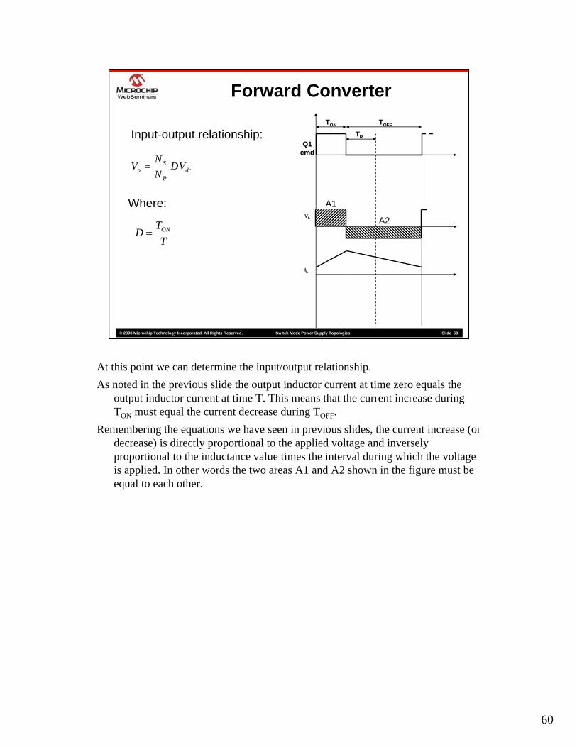
At this point we can determine the input/output relationship.As noted in the previous slide the output inductor current at time zero equals the
output inductor current at time T. This means that the current increase during TON must equal the current decrease during TOFF.
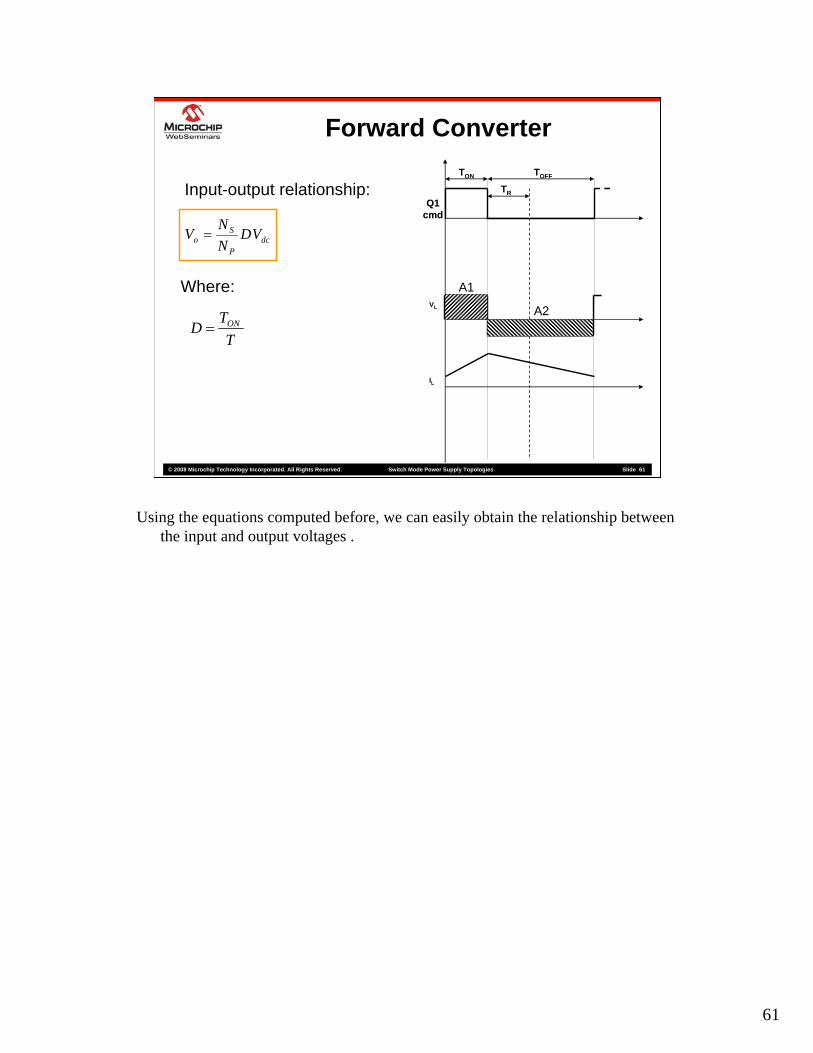
Remembering the equations we have seen in previous slides, the current increase (or decrease) is directly proportional to the applied voltage and inversely proportional to the inductance value times the interval during which the voltage is applied. In other words the two areas A1 and A2 shown in the figure must be equal to each other.
61
© 2008 Microchip Technology Incorporated. All Rights Reserved. Switch Mode Power Supply Topologies Slide 61
Forward Converter
Input-output relationship:Q1Q1
cmdcmd
TON TOFF
VL
IL
TR
A1
A2
dcP
So VD
NN
V =
Where:
TT
D ON=
Using the equations computed before, we can easily obtain the relationship between the input and output voltages .

62
© 2008 Microchip Technology Incorporated. All Rights Reserved. Switch Mode Power Supply Topologies Slide 62
Forward Converter
Input-output relationship:Q1Q1
cmdcmd
TON TOFF
VL
IL
TR
A1
A2
dcP
So VD
NN
V =
Where:
TT
D ON=
The relationship is linear and it is proportional to:1. D, which is the duty cycle , and to2. The ratio (Ns / Np),which is the transformer windings turns ratio.This is an important result. It tells us that the transformer turns ratio can also be
used to define, in the design step, the output voltage value.

63
© 2008 Microchip Technology Incorporated. All Rights Reserved. Switch Mode Power Supply Topologies Slide 63
Forward Converter
Design Equations: Transformer primary
Flux change during TON:
coreP
ONP
ANTV
B =Δ
Solving respect to NP and considering to run the system at maximum TON:
min,max
dccorePWM
P VBAF
DN
Δ=
BAFV
NcorePWM
oS Δ=
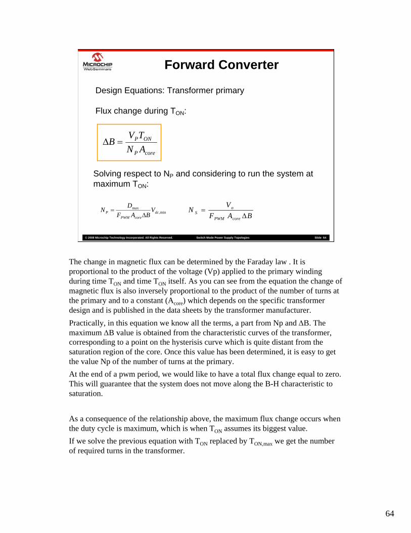
Design Equations.We will now present the design equations.Let us start with the selection of the magnetics. During a switching period the transformer core operates along its hysterisis curve in its B-H plot.
64
© 2008 Microchip Technology Incorporated. All Rights Reserved. Switch Mode Power Supply Topologies Slide 64
Forward Converter
Design Equations: Transformer primary
Flux change during TON:
coreP
ONP
ANTV
B =Δ
Solving respect to NP and considering to run the system at maximum TON:
min,max
dccorePWM
P VBAF
DN
Δ=
BAFV
NcorePWM
oS Δ=
The change in magnetic flux can be determined by the Faraday law . It is proportional to the product of the voltage (Vp) applied to the primary winding during time TON and time TON itself. As you can see from the equation the change of magnetic flux is also inversely proportional to the product of the number of turns at the primary and to a constant (Acore) which depends on the specific transformer design and is published in the data sheets by the transformer manufacturer.Practically, in this equation we know all the terms, a part from Np and ΔB. The maximum ΔB value is obtained from the characteristic curves of the transformer, corresponding to a point on the hysterisis curve which is quite distant from the saturation region of the core. Once this value has been determined, it is easy to get the value Np of the number of turns at the primary.At the end of a pwm period, we would like to have a total flux change equal to zero. This will guarantee that the system does not move along the B-H characteristic to saturation.
As a consequence of the relationship above, the maximum flux change occurs when the duty cycle is maximum, which is when TON assumes its biggest value.If we solve the previous equation with TON replaced by TON,max we get the number of required turns in the transformer.

65
© 2008 Microchip Technology Incorporated. All Rights Reserved. Switch Mode Power Supply Topologies Slide 65
Forward Converter
Design Equations: Transformer primary
Flux change during TON:
coreP
ONP
ANTV
B =Δ
Solving respect to NP and considering to run the system at maximum TON:
min,max
dccorePWM
P VBAF
DN
Δ=
BAFV
NcorePWM
oS Δ=
The dependance of the number of primary turns from the maximum value of the TON period, is expressed in this equation by the term Dmax.

66
© 2008 Microchip Technology Incorporated. All Rights Reserved. Switch Mode Power Supply Topologies Slide 66
Forward Converter
Design Equations: Transformer primary
Flux change during TON:
coreP
ONP
ANTV
B =Δ
Solving respect to NP and considering to run the system at maximum TON:
min,max
dccorePWM
P VBAF
DN
Δ=
BAFV
NcorePWM
oS Δ=
Moreover using the input/output relationship we found in the previous slide, we can also easily determine the number of turns at the secondary to sustain the specified output voltage Vo.

67
© 2008 Microchip Technology Incorporated. All Rights Reserved. Switch Mode Power Supply Topologies Slide 67
Forward Converter
Design Equations: Mosfet
Voltage on Q1:
Q1Q1cmdcmd
TON TOFF
TR
Vdc
2 Vdc
dcR
PoffQ V
NNV ⎟⎟
⎠
⎞⎜⎜⎝
⎛+= 1,
offQQ VV ,max, 3.1=
With some margin::
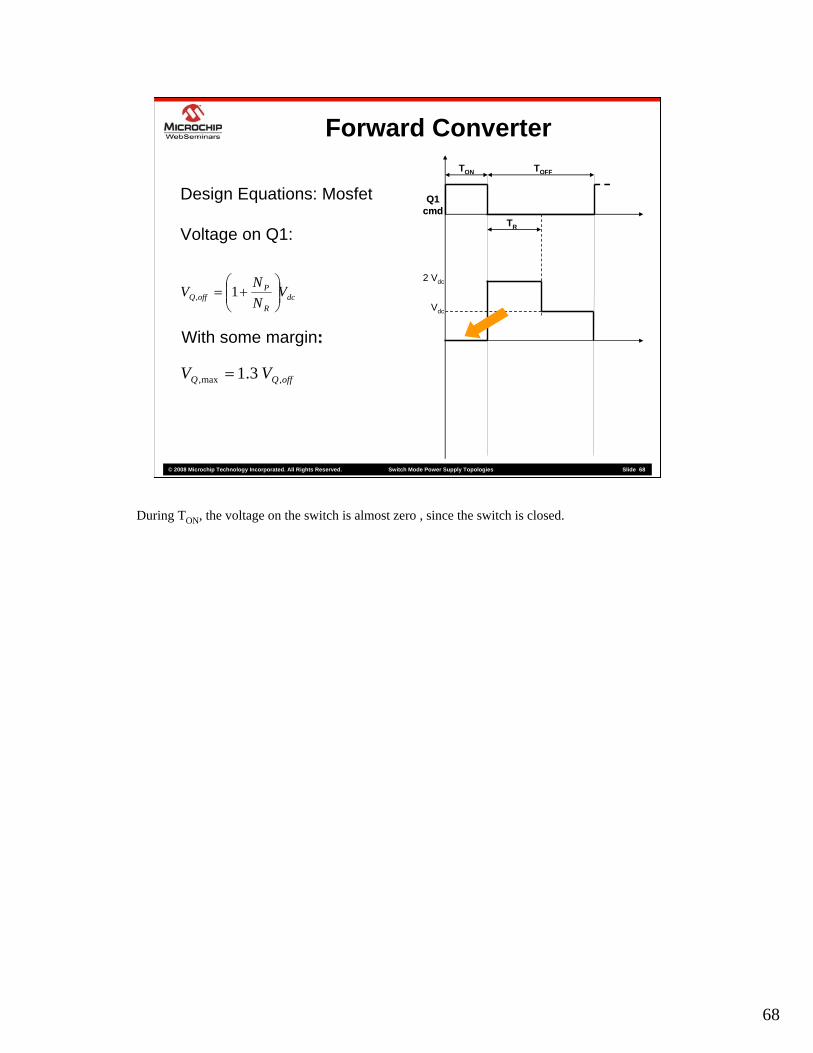
Design Equations: Mosfet selection.The selection of the MOSFET switch should be done analyzing the maximum voltage it has to withstand.
68
© 2008 Microchip Technology Incorporated. All Rights Reserved. Switch Mode Power Supply Topologies Slide 68
Forward Converter
Design Equations: Mosfet
Voltage on Q1:
Q1Q1cmdcmd
TON TOFF
TR
Vdc
2 Vdc
dcR
PoffQ V
NNV ⎟⎟
⎠
⎞⎜⎜⎝
⎛+= 1,
offQQ VV ,max, 3.1=
With some margin::
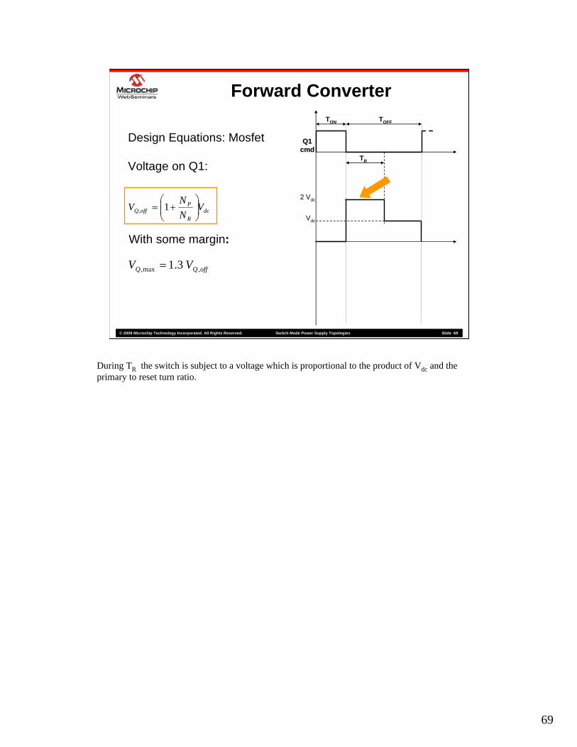
During TON, the voltage on the switch is almost zero , since the switch is closed.
69
© 2008 Microchip Technology Incorporated. All Rights Reserved. Switch Mode Power Supply Topologies Slide 69
Forward Converter
Design Equations: Mosfet
Voltage on Q1:
Q1Q1cmdcmd
TON TOFF
TR
Vdc
2 Vdc
dcR
PoffQ V
NNV ⎟⎟
⎠
⎞⎜⎜⎝
⎛+= 1,
offQQ VV ,max, 3.1=
With some margin::
During TR the switch is subject to a voltage which is proportional to the product of Vdc and the primary to reset turn ratio.

70
© 2008 Microchip Technology Incorporated. All Rights Reserved. Switch Mode Power Supply Topologies Slide 70
Forward Converter
Design Equations: Mosfet
Voltage on Q1:
Q1Q1cmdcmd
TON TOFF
TR
Vdc
2 Vdc
dcR
PoffQ V
NNV ⎟⎟
⎠
⎞⎜⎜⎝
⎛+= 1,
offQQ VV ,max, 3.1=
With some margin::
During the time interval from (TON + TR) to T the voltage on the switch is Vdc.
The maximum current that is flowing through the switch is the sum of the magnetizing current and the load current reflected back into the primary.The Np / Nr ratio gives us an additional degree of freedom, to set the output voltage level. But on the other side it also is responsible for an increase on the voltage that must be sustained by the switch. In the case where NP = NR, the voltage on Q1 is twice the input voltage (as shown in the figure)
Because of spikes due to leakage current, a margin of about 30% is normally used, so that the total voltage on the switch is greater than what is computed by the equation.

71
© 2008 Microchip Technology Incorporated. All Rights Reserved. Switch Mode Power Supply Topologies Slide 71
Forward Converter
Design Equations: Mosfet
Voltage on Q1:
Q1Q1cmdcmd
TON TOFF
TR
Vdc
2 Vdc
dcR
PoffQ V
NNV ⎟⎟
⎠
⎞⎜⎜⎝
⎛+= 1,
offQQ VV ,max, 3.1=
With some margin::
Because of spikes due to leakage current, a margin of about 30% is normally used, so that the total voltage on the switch is greater than what is computed by the equation.

72
© 2008 Microchip Technology Incorporated. All Rights Reserved. Switch Mode Power Supply Topologies Slide 72
Forward Converter
Q1Q1cmdcmd
TON TOFF
TR
max,max,3
max,max,2
max,max,1 1
dcP
SD
dcR
SD
dcP
RD
VNN
V
VNN
V
VNN
V
−=
−=
⎟⎟⎠
⎞⎜⎜⎝
⎛+−=
Diodes selection:
VD1
VD2
VD3
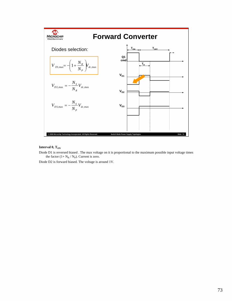
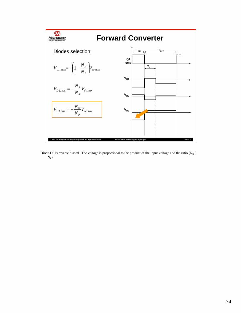
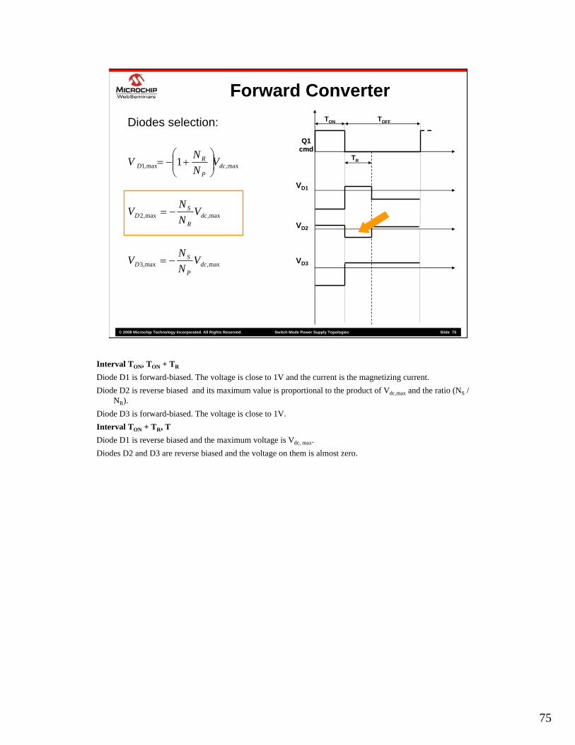
Design Equations: Diodes.In order to select the diodes used in the forward converter we have to analyze the maximum current and voltage
they have to sustain. Note that we can only be in one of the following two conditions at any time:1. The diode is conducting: the voltage across the diode is close to 1V (its real value depends on the type of
diode and the intensity of the flowing current). The current is detemined by the rest of the external circuit (and the diode must be dimensioned in order to be able to sustain such a current)
2. The diode is not conducting: The current through the diode is zero (because it operates as an open circuit), but the voltage is imposed by the rest of the circuit. And, as for the current, we must ensure that the diode can withstand such a voltage.
If we consider the three intervals of time in which the pwm period is split, we see that:
73
© 2008 Microchip Technology Incorporated. All Rights Reserved. Switch Mode Power Supply Topologies Slide 73
Forward Converter
Q1Q1cmdcmd
TON TOFF
TR
max,max,3
max,max,2
max,max,1 1
dcP
SD
dcR
SD
dcP
RD
VNN
V
VNN
V
VNN
V
−=
−=
⎟⎟⎠
⎞⎜⎜⎝
⎛+−=
Diodes selection:
VD1
VD2
VD3
Interval 0, TON
Diode D1 is reversed biased . The max voltage on it is proportional to the maximum possible input voltage times the factor (1+ NR / NP). Current is zero.
Diode D2 is forward biased. The voltage is around 1V.
74
© 2008 Microchip Technology Incorporated. All Rights Reserved. Switch Mode Power Supply Topologies Slide 74
Forward Converter
Q1Q1cmdcmd
TON TOFF
TR
max,max,3
max,max,2
max,max,1 1
dcP
SD
dcR
SD
dcP
RD
VNN
V
VNN
V
VNN
V
−=
−=
⎟⎟⎠
⎞⎜⎜⎝
⎛+−=
Diodes selection:
VD1
VD2
VD3
Diode D3 is reverse biased . The voltage is proportional to the product of the input voltage and the ratio (NS / NP)
75
© 2008 Microchip Technology Incorporated. All Rights Reserved. Switch Mode Power Supply Topologies Slide 75
Forward Converter
Q1Q1cmdcmd
TON TOFF
TR
max,max,3
max,max,2
max,max,1 1
dcP
SD
dcR
SD
dcP
RD
VNN
V
VNN
V
VNN
V
−=
−=
⎟⎟⎠
⎞⎜⎜⎝
⎛+−=
Diodes selection:
VD1
VD2
VD3
Interval TON, TON + TR
Diode D1 is forward-biased. The voltage is close to 1V and the current is the magnetizing current.Diode D2 is reverse biased and its maximum value is proportional to the product of Vdc,max and the ratio (NS /
NR).Diode D3 is forward-biased. The voltage is close to 1V.Interval TON + TR, TDiode D1 is reverse biased and the maximum voltage is Vdc, max.Diodes D2 and D3 are reverse biased and the voltage on them is almost zero.
76
© 2008 Microchip Technology Incorporated. All Rights Reserved. Switch Mode Power Supply Topologies Slide 76
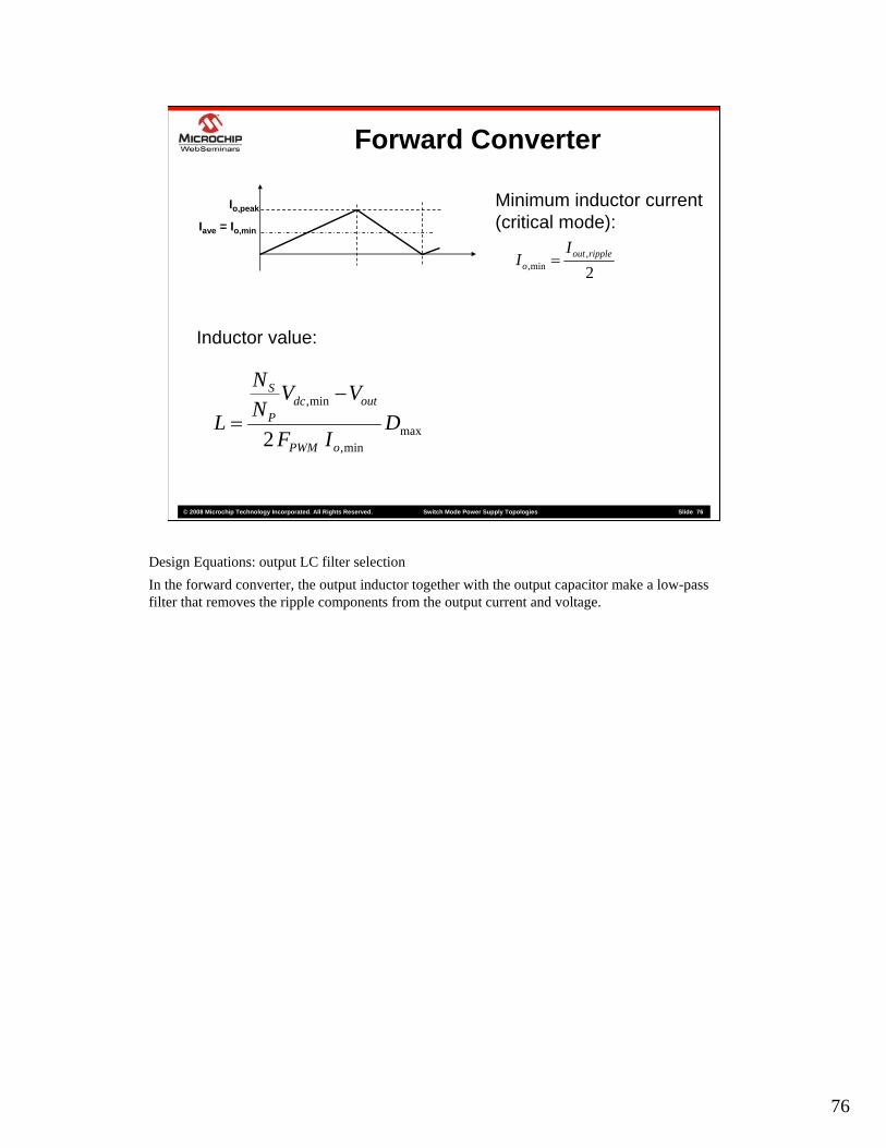
Forward Converter
Iave = Io,min
Io,peak
2,
min,rippleout
o
II =
Minimum inductor current(critical mode):
maxmin,
min,
2D
IF
VVNN
LoPWM
outdcP
S −=
Inductor value:
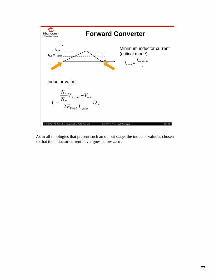
Design Equations: output LC filter selectionIn the forward converter, the output inductor together with the output capacitor make a low-pass filter that removes the ripple components from the output current and voltage.
77
© 2008 Microchip Technology Incorporated. All Rights Reserved. Switch Mode Power Supply Topologies Slide 77
Forward Converter
Iave = Io,min
Io,peak
2,
min,rippleout
o
II =
Minimum inductor current(critical mode):
maxmin,
min,
2D
IF
VVNN
LoPWM
outdcP
S −=
Inductor value:
As in all topologies that present such an output stage, the inductor value is chosen so that the inductor current never goes below zero .
78
© 2008 Microchip Technology Incorporated. All Rights Reserved. Switch Mode Power Supply Topologies Slide 78
Forward Converter
Iave = Io,min
Io,peak
2,
min,rippleout
o
II =
Minimum inductor current(critical mode):
maxmin,
min,
2D
IF
VVNN
LoPWM
outdcP
S −=
Inductor value:
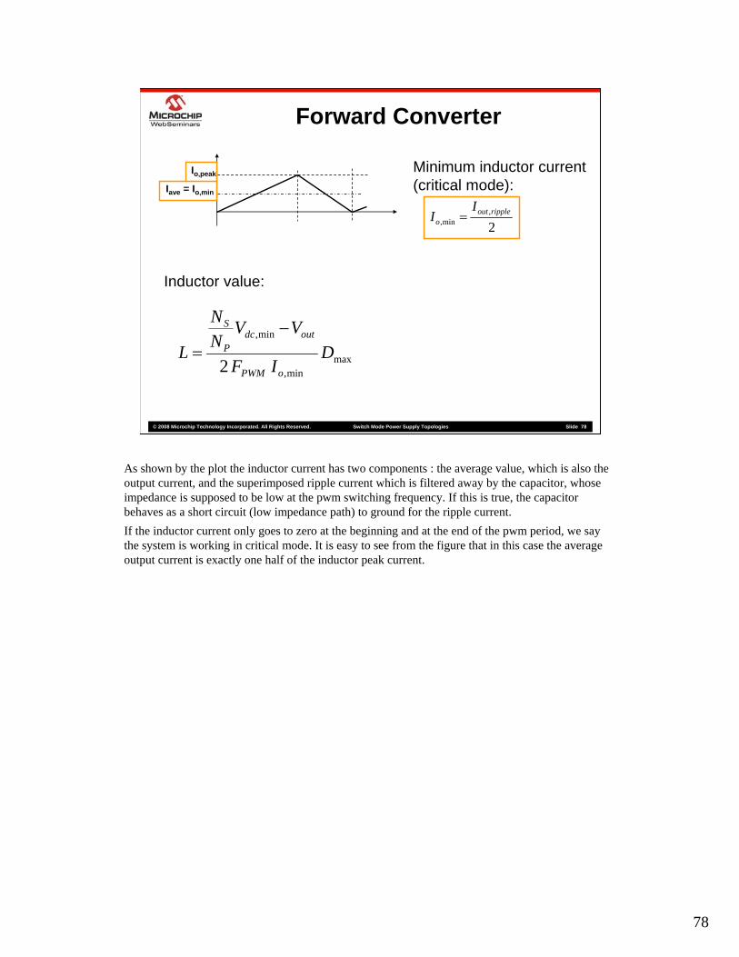
As shown by the plot the inductor current has two components : the average value, which is also the output current, and the superimposed ripple current which is filtered away by the capacitor, whose impedance is supposed to be low at the pwm switching frequency. If this is true, the capacitor behaves as a short circuit (low impedance path) to ground for the ripple current.If the inductor current only goes to zero at the beginning and at the end of the pwm period, we say the system is working in critical mode. It is easy to see from the figure that in this case the average output current is exactly one half of the inductor peak current.
79
© 2008 Microchip Technology Incorporated. All Rights Reserved. Switch Mode Power Supply Topologies Slide 79
Forward Converter
Iave = Io,min
Io,peak
2,
min,rippleout
o
II =
Minimum inductor current(critical mode):
maxmin,
min,
2D
IF
VVNN
LoPWM
outdcP
S −=
Inductor value:
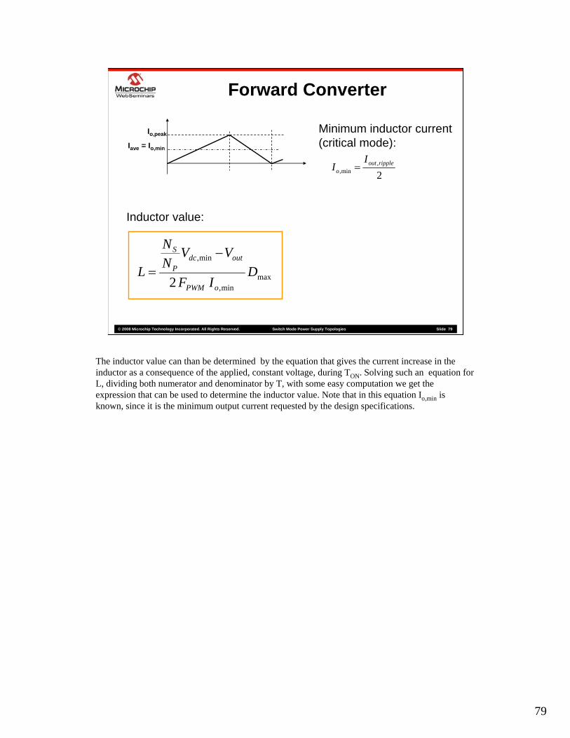
The inductor value can than be determined by the equation that gives the current increase in the inductor as a consequence of the applied, constant voltage, during TON. Solving such an equation for L, dividing both numerator and denominator by T, with some easy computation we get the expression that can be used to determine the inductor value. Note that in this equation Io,min is known, since it is the minimum output current requested by the design specifications.

80
© 2008 Microchip Technology Incorporated. All Rights Reserved. Switch Mode Power Supply Topologies Slide 80
Forward Converter
Design Equations: Output CapacitorContributions:1. Capacitor model equivalent resistace (RESR):
( ) LESRESRESRr IRIIRV Δ=−= 12,
∫= dttiC
V cCr )(10,
[ ]LESRtotalrPWM
L
IRVFDIC
Δ−ΔΔ
=,
0
2. voltage drop on the capacitor (Vr,Co):
Summing and rearranging terms, we have:
Design Equations: Output CapacitorAs we have seen in the previous slide the capacitor impedance sould be as low as possible to appear as a short circuit to ground for the ripple current flowing into the inductor.The selection of the output capacitor is related to the maximum amount of ripple voltage allowed by the design specifications. We consequently have to analyze with some detail, what are the contributions to the output ripple. To do so, we should consider the capacitor equivalent circuit, where we have an ideal capacitor, plus a resistor. In the model you can also normally find an inductor but its value is normally such that it does not significantly influence the output ripple amplitude.

81
© 2008 Microchip Technology Incorporated. All Rights Reserved. Switch Mode Power Supply Topologies Slide 81
Forward Converter
Design Equations: Output CapacitorContributions:1. Capacitor model equivalent resistace (RESR):
( ) LESRESRESRr IRIIRV Δ=−= 12,
∫= dttiC
V cCr )(10,
[ ]LESRtotalrPWM
L
IRVFDIC
Δ−ΔΔ
=,
0
2. voltage drop on the capacitor (Vr,Co):
Summing and rearranging terms, we have:
The presence of a resistor in the model (RESR), has as a consequence that the inductor ripple current will generate a ripple voltage at its terminals.

82
© 2008 Microchip Technology Incorporated. All Rights Reserved. Switch Mode Power Supply Topologies Slide 82
Forward Converter
Design Equations: Output CapacitorContributions:1. Capacitor model equivalent resistace (RESR):
( ) LESRESRESRr IRIIRV Δ=−= 12,
∫= dttiC
V cCr )(10,
[ ]LESRtotalrPWM
L
IRVFDIC
Δ−ΔΔ
=,
0
2. voltage drop on the capacitor (Vr,Co):
Summing and rearranging terms, we have:
The second contribution directly comes from the capacitor . Current flowing into the capacitor will generate a voltage drop which can be computed as the integral over time of the current itself. The capacitor value appears in this equation as a proportionality factor.Summing these two contributions gives the maximum ripple voltage that will be developed at the capacitor terminals. This value must be lower than the maximum acceptable ripple voltage, as defined by design specifications.

83
© 2008 Microchip Technology Incorporated. All Rights Reserved. Switch Mode Power Supply Topologies Slide 83
Forward Converter
Design Equations: Output CapacitorContributions:1. Capacitor model equivalent resistace (RESR):
( ) LESRESRESRr IRIIRV Δ=−= 12,
∫= dttiC
V cCr )(10,
[ ]LESRtotalrPWM
L
IRVFDIC
Δ−ΔΔ
=,
0
2. voltage drop on the capacitor (Vr,Co):
Summing and rearranging terms, we have:
With some computation , it is easy to determine the value of the capacitor as shown by the last equation.

84
© 2008 Microchip Technology Incorporated. All Rights Reserved. Switch Mode Power Supply Topologies Slide 84
Thank You
Thank you for attending this WebSeminar. For more information please visit the microchip website at www.microchip.com


![Ethernet Switch Enhanced [Compatibility Mode]](https://img.pdfslide.us/doc/110x75/5695cfd31a28ab9b028fb725/ethernet-switch-enhanced-compatibility-mode.jpg)