Embed Size (px)
Citation preview
© KEMET Electronics Corporation • P.O. Box 5928 • Greenville, SC 29606 • 864-963-6300 • www.kemet.com C1035_C0G_PULSE_SMD • 5/25/2018 1One world. One KEMET
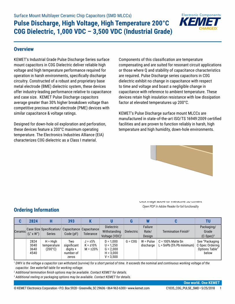
Ordering Information
C 2824 H 393 K U G W C TU
CeramicCase Size (L" x W")
Specification/Series
Capacitance Code (pF)
Capacitance Tolerance
Dielectric Withstanding
Voltage (VDC)1
DielectricFailure Rate/
DesignTermination Finish2
Packaging/ Grade
(C-Spec)3
2824304036404540
H = High temperature
(200°C)
Two significant
digits + number of
zeros
J = ±5%K = ±10%M = ±20%
D = 1,000U = 1,250G = 2,000H = 3,000V = 3,500
G = C0G W = Pulse discharge
C = 100% Matte SnL = SnPb (5% Pb minimum)
See “Packaging C-Spec Ordering Options Table”
below
1 DWV is the voltage a capacitor can withstand (survive) for a short period of time. It exceeds the nominal and continuous working voltage of the capacitor. See waterfall table for working voltage.
2 Additional termination finish options may be available. Contact KEMET for details.3 Additional reeling or packaging options may be available. Contact KEMET for details.
Overview
KEMET’s Industrial Grade Pulse Discharge Series surface mount capacitors in C0G Dielectric deliver reliable high voltage and high temperature performance required for operation in harsh environments, specifically discharge circuitry. Constructed of a robust and proprietary base metal electrode (BME) dielectric system, these devices offer industry-leading performance relative to capacitance and case size. KEMET Pulse Discharge capacitors average greater than 30% higher breakdown voltage than competitive precious metal electrode (PME) devices with similar capacitance & voltage ratings.
Designed for down-hole oil exploration and perforation, these devices feature a 200°C maximum operating temperature. The Electronics Industries Alliance (EIA) characterizes C0G dielectric as a Class I material.
Components of this classification are temperature compensating and are suited for resonant circuit applications or those where Q and stability of capacitance characteristics are required. Pulse Discharge series capacitors in C0G dielectric exhibit no change in capacitance with respect to time and voltage and boast a negligible change in capacitance with reference to ambient temperature. These devices retain high insulation resistance with low dissipation factor at elevated temperatures up 200°C.
KEMET’s Pulse Discharge surface mount MLCCs are manufactured in state-of-the-art ISO/TS 16949:2009 certified facilities and are proven to function reliably in harsh, high temperature and high humidity, down-hole environments.
Surface Mount Multilayer Ceramic Chip Capacitors (SMD MLCCs)
Pulse Discharge, High Voltage, High Temperature 200°CC0G Dielectric, 1,000 VDC – 3,500 VDC (Industrial Grade)
© KEMET Electronics Corporation • P.O. Box 5928 • Greenville, SC 29606 • 864-963-6300 • www.kemet.com C1035_C0G_PULSE_SMD • 5/25/2018 2
Surface Mount Multilayer Ceramic Chip Capacitors (SMD MLCCs)Pulse Discharge, High Voltage, High Temperature 200°C C0G Dielectric, 1,000 VDC – 3,500 VDC (Industrial Grade)
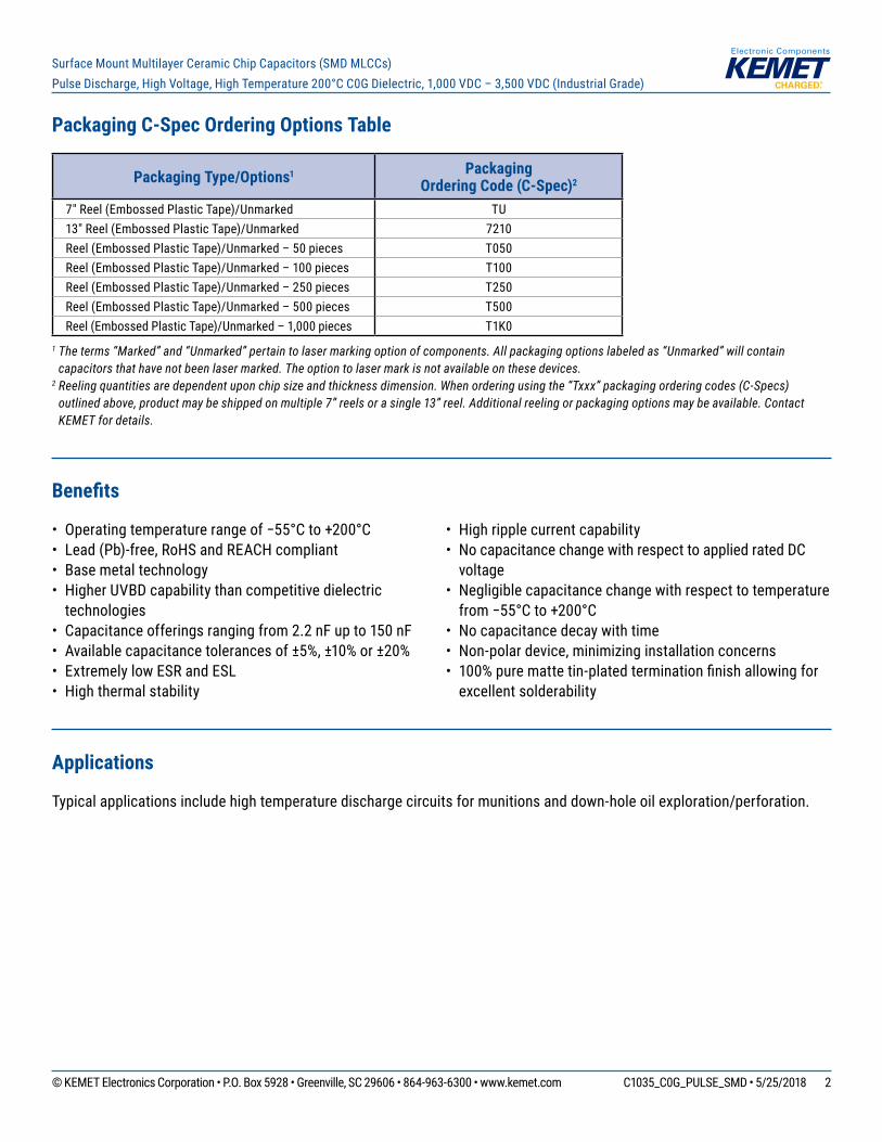
Packaging C-Spec Ordering Options Table
Packaging Type/Options1 Packaging Ordering Code (C-Spec)2
7" Reel (Embossed Plastic Tape)/Unmarked TU13" Reel (Embossed Plastic Tape)/Unmarked 7210Reel (Embossed Plastic Tape)/Unmarked – 50 pieces T050Reel (Embossed Plastic Tape)/Unmarked – 100 pieces T100Reel (Embossed Plastic Tape)/Unmarked – 250 pieces T250Reel (Embossed Plastic Tape)/Unmarked – 500 pieces T500Reel (Embossed Plastic Tape)/Unmarked – 1,000 pieces T1K0
1 The terms “Marked” and “Unmarked” pertain to laser marking option of components. All packaging options labeled as “Unmarked” will contain capacitors that have not been laser marked. The option to laser mark is not available on these devices.
2 Reeling quantities are dependent upon chip size and thickness dimension. When ordering using the “Txxx” packaging ordering codes (C-Specs) outlined above, product may be shipped on multiple 7” reels or a single 13” reel. Additional reeling or packaging options may be available. Contact KEMET for details.
Benefits
• Operating temperature range of −55°C to +200°C• Lead (Pb)-free, RoHS and REACH compliant• Base metal technology• Higher UVBD capability than competitive dielectric
technologies• Capacitance offerings ranging from 2.2 nF up to 150 nF• Available capacitance tolerances of ±5%, ±10% or ±20%• Extremely low ESR and ESL• High thermal stability
• High ripple current capability• No capacitance change with respect to applied rated DC
voltage• Negligible capacitance change with respect to temperature
from −55°C to +200°C• No capacitance decay with time• Non-polar device, minimizing installation concerns• 100% pure matte tin-plated termination finish allowing for
excellent solderability
Applications
Typical applications include high temperature discharge circuits for munitions and down-hole oil exploration/perforation.
© KEMET Electronics Corporation • P.O. Box 5928 • Greenville, SC 29606 • 864-963-6300 • www.kemet.com C1035_C0G_PULSE_SMD • 5/25/2018 3
Surface Mount Multilayer Ceramic Chip Capacitors (SMD MLCCs)Pulse Discharge, High Voltage, High Temperature 200°C C0G Dielectric, 1,000 VDC – 3,500 VDC (Industrial Grade)
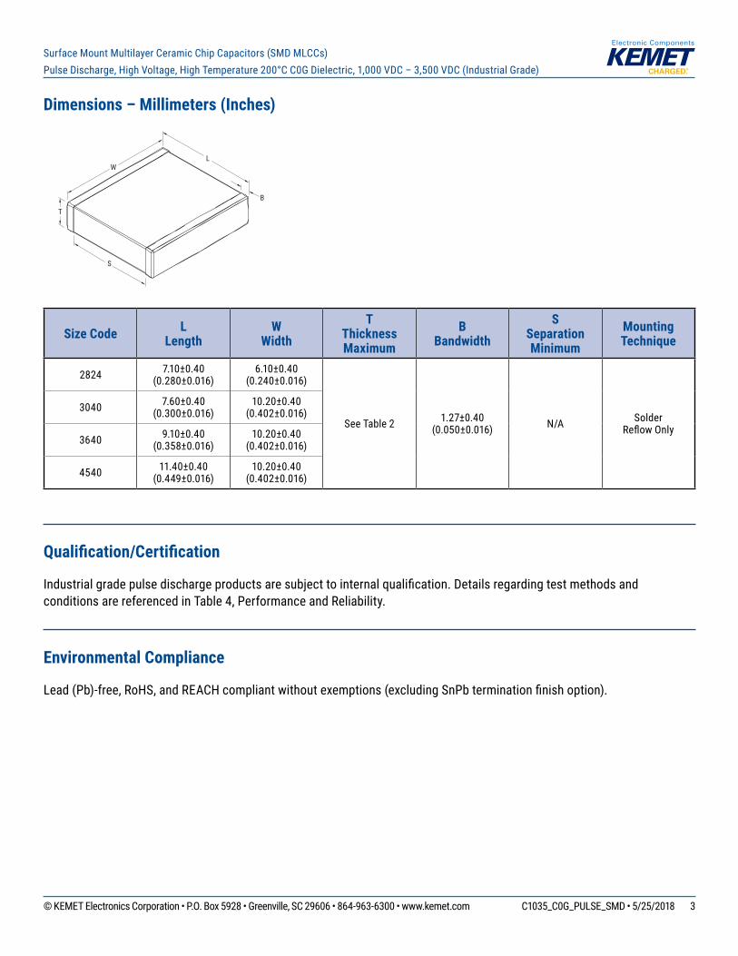
Dimensions – Millimeters (Inches)
T
S
W L
B
Size Code L Length
W Width
T Thickness Maximum
B Bandwidth
SSeparation Minimum
Mounting Technique
2824 7.10±0.40 (0.280±0.016)
6.10±0.40 (0.240±0.016)
See Table 2 1.27±0.40(0.050±0.016) N/A Solder
Reflow Only
3040 7.60±0.40 (0.300±0.016)
10.20±0.40 (0.402±0.016)
3640 9.10±0.40 (0.358±0.016)
10.20±0.40 (0.402±0.016)
4540 11.40±0.40 (0.449±0.016)
10.20±0.40 (0.402±0.016)
Qualification/Certification
Industrial grade pulse discharge products are subject to internal qualification. Details regarding test methods and conditions are referenced in Table 4, Performance and Reliability.
Environmental Compliance
Lead (Pb)-free, RoHS, and REACH compliant without exemptions (excluding SnPb termination finish option).
© KEMET Electronics Corporation • P.O. Box 5928 • Greenville, SC 29606 • 864-963-6300 • www.kemet.com C1035_C0G_PULSE_SMD • 5/25/2018 4
Surface Mount Multilayer Ceramic Chip Capacitors (SMD MLCCs)Pulse Discharge, High Voltage, High Temperature 200°C C0G Dielectric, 1,000 VDC – 3,500 VDC (Industrial Grade)
Electrical Parameters/Characteristics
Item Parameters/CharacteristicsOperating Temperature Range −55°C to +200°C
Capacitance Change with Reference to +25°C and 0 VDC Applied (TCC) ±30 ppm/ºC
Aging Rate (Maximum % Capacitance Loss/Decade Hour) 0%
1Dielectric Withstanding Voltage (DWV) See product selection table (product waterfall) for available ratings
2Dissipation Factor (DF) Maximum Limit at 25ºC 0.1%
3Insulation Resistance (IR) Minimum Limit at 25°C 1,000 megohm microfarads or 100 GΩ (500 VDC applied for 120±5 seconds at 25°C)
1 DWV is the voltage a capacitor can withstand (survive) for a short period of time. It exceeds the nominal and continuous working voltage of the capacitor.
2 Capacitance and dissipation factor (DF) measured under the following conditions: 1 MHz ±100 kHz and 1.0 Vrms ±0.2 V if capacitance ≤ 1,000 pF 1 kHz ± 50 Hz and 1.0 Vrms ±0.2 V if capacitance > 1,000 pF3 To obtain IR limit, divide MΩ-µF value by the capacitance and compare to GΩ limit. Select the lower of the two limits.Note: When measuring capacitance it is important to ensure the set voltage level is held constant. The HP4284 and Agilent E4980 have a feature known as Automatic Level Control (ALC). The ALC feature should be switched to “ON.”
Post Environmental Limits
High Temperature Life, Biased Humidity, Moisture Resistance
Dielectric Rated DCVoltage
CapacitanceValue
Dissipation Factor (Maximum %)
CapacitanceShift
Insulation Resistance
C0G All All 0.5 0.3% or ±0.25 pF 10% of Initial Limit
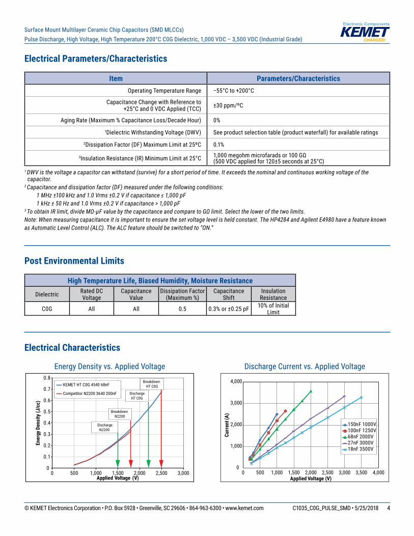
Electrical Characteristics
Discharge Current vs. Applied Voltage
0
1,000
2,000
3,000
4,000
0 500 1,000 1,500 2,000 2,500 3,000 3,500 4,000
Curr
ent (
A)
Applied Voltage (V)
150nF 1000V100nF 1250V68nF 2000V27nF 3000V18nF 3500V
Energy Density vs. Applied Voltage
0
0.1
0.2
0.3
0.4
0.5
0.6
0.7
0.8
0 500 1,000 1,500 2,000 2,500 3,000
Ener
gy D
ensi
ty (J
/cc)
Applied Voltage (V)
KEMET HT C0G 4540 68nF
Competitor N2200 3640 200nF
Breakdown HT C0G
BreakdownN2200
DischargeN2200
DischargeHT C0G
© KEMET Electronics Corporation • P.O. Box 5928 • Greenville, SC 29606 • 864-963-6300 • www.kemet.com C1035_C0G_PULSE_SMD • 5/25/2018 5
Surface Mount Multilayer Ceramic Chip Capacitors (SMD MLCCs)Pulse Discharge, High Voltage, High Temperature 200°C C0G Dielectric, 1,000 VDC – 3,500 VDC (Industrial Grade)
Table 1 – Pulse Discharge Series, Capacitance Range Waterfall
These products are protected under US Patents 7,172,985 and 7,670,981, other patents pending, and any foreign counterparts.
Capacitance Cap Code
Case Size/ Series C2824H C3040H C3640H C4540H
Voltage Code D U G H V D U G H V D U G H V D U G H V
Dielectric Withstanding Voltage (DWV) 10
00
1250
2000
3000
3500
1000
1250
2000
3000
3500
1000
1250
2000
3000
3500
1000
1250
2000
3000
3500
Working Voltage 500
630
1000
1500
2000
500
630
1000
1500
2000
500
630
1000
1500
2000
500
630
1000
1500
2000
Capacitance Tolerance Product Availability and Chip Thickness Codes See Table 2 for Chip Thickness Dimensions
1,800 pF 182 J K M2,000 pF 202 J K M2,200 pF 222 J K M TA TA TA TA TA2,700 pF 272 J K M TA TA TA TA TA3,300 pF 332 J K M TA TA TA TA TA QB QB QB QB QB3,900 pF 392 J K M TA TA TA TA TB QB QB QB QB QB MA MA MA MA MA4,700 pF 472 J K M TA TA TA TB TB QB QB QB QB QB MA MA MA MA MA SA SA SA SA SA5,600 pF 562 J K M TA TA TA TB TC QB QB QB QB QB MA MA MA MA MA SA SA SA SA SA6,800 pF 682 J K M TA TA TA TB QB QB QB QB QC MA MA MA MA MA SA SA SA SA SA8,200 pF 822 J K M TA TA TA TC QB QB QB QC QC MA MA MA MA MB SA SA SA SA SA
10,000 pF 103 J K M TA TA TA QB QB QB QC QD MA MA MA MA MB SA SA SA SA SB12,000 pF 123 J K M TA TA TA QB QB QB QD MA MA MA MB MB SA SA SA SA SB15,000 pF 153 J K M TA TA TB QB QB QB QD MA MA MA MB MC SA SA SA SB SB18,000 pF 183 J K M TA TA TB QB QB QB MA MA MA MC SA SA SA SB SC22,000 pF 223 J K M TA TB TC QB QB QC MA MA MA SA SA SA SB27,000 pF 273 J K M TA TB QB QB QC MA MA MA SA SA SA SC33,000 pF 333 J K M TB TB QB QC QC MA MA MB SA SA SA39,000 pF 393 J K M TB TC QB QC QD MA MA MB SA SA SB47,000 pF 473 J K M TB QB QC MA MB MC SA SA SB56,000 pF 563 J K M TC QC QD MA MB SA SA SB68,000 pF 683 J K M QC QD MB MC SA SB SC82,000 pF 823 J K M QC MB SA SB
0.10 µF 104 J K M QD MC SB SC0.12 µF 124 J K M MC SB0.15 µF 154 J K M SC
Capacitance Cap Code
Working Voltage 500
630
1000
1500
2000
500
630
1000
1500
2000
500
630
1000
1500
2000
500
630
1000
1500
2000
Dielectric Withstanding Voltage (DWV) 10
00
1250
2000
3000
3500
1000
1250
2000
3000
3500
1000
1250
2000
3000
3500
1000
1250
2000
3000
3500
Voltage Code D U G H V D U G H V D U G H V D U G H V
Case Size/Series C2824H C3040H C3640H C4540H
© KEMET Electronics Corporation • P.O. Box 5928 • Greenville, SC 29606 • 864-963-6300 • www.kemet.com C1035_C0G_PULSE_SMD • 5/25/2018 6
Surface Mount Multilayer Ceramic Chip Capacitors (SMD MLCCs)Pulse Discharge, High Voltage, High Temperature 200°C C0G Dielectric, 1,000 VDC – 3,500 VDC (Industrial Grade)
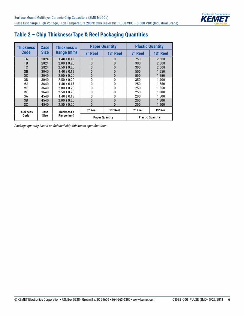
Table 2 – Chip Thickness/Tape & Reel Packaging Quantities
Thickness Code
Case Size
Thickness ± Range (mm)
Paper Quantity Plastic Quantity7" Reel 13" Reel 7" Reel 13" Reel
TA 2824 1.40 ± 0.15 0 0 750 2,500TB 2824 2.00 ± 0.20 0 0 300 2,000 TC 2824 2.50 ± 0.20 0 0 300 2,000 QB 3040 1.40 ± 0.15 0 0 500 1,650QC 3040 2.00 ± 0.20 0 0 500 1,650QD 3040 2.50 ± 0.20 0 0 350 1,400MA 3640 1.40 ± 0.15 0 0 250 1,550MB 3640 2.00 ± 0.20 0 0 250 1,550MC 3640 2.50 ± 0.20 0 0 250 1,000SA 4540 1.40 ± 0.15 0 0 200 1,500SB 4540 2.00 ± 0.20 0 0 200 1,500SC 4540 2.50 ± 0.20 0 0 200 1,500
Thickness Code
Case Size
Thickness ± Range (mm)
7" Reel 13" Reel 7" Reel 13" Reel
Paper Quantity Plastic Quantity
Package quantity based on finished chip thickness specifications.
© KEMET Electronics Corporation • P.O. Box 5928 • Greenville, SC 29606 • 864-963-6300 • www.kemet.com C1035_C0G_PULSE_SMD • 5/25/2018 7
Surface Mount Multilayer Ceramic Chip Capacitors (SMD MLCCs)Pulse Discharge, High Voltage, High Temperature 200°C C0G Dielectric, 1,000 VDC – 3,500 VDC (Industrial Grade)
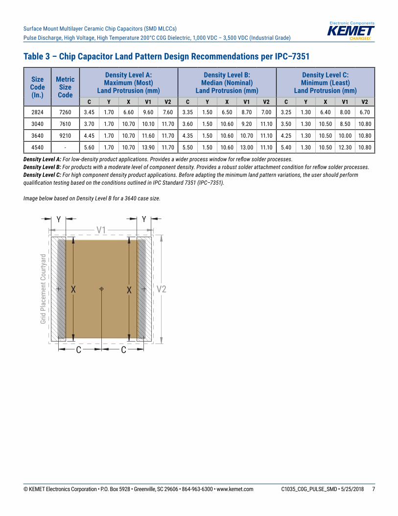
Table 3 – Chip Capacitor Land Pattern Design Recommendations per IPC–7351
Size Code (In.)
Metric Size Code
Density Level A: Maximum (Most)
Land Protrusion (mm)
Density Level B: Median (Nominal)
Land Protrusion (mm)
Density Level C: Minimum (Least)
Land Protrusion (mm)C Y X V1 V2 C Y X V1 V2 C Y X V1 V2
2824 7260 3.45 1.70 6.60 9.60 7.60 3.35 1.50 6.50 8.70 7.00 3.25 1.30 6.40 8.00 6.70
3040 7610 3.70 1.70 10.70 10.10 11.70 3.60 1.50 10.60 9.20 11.10 3.50 1.30 10.50 8.50 10.80
3640 9210 4.45 1.70 10.70 11.60 11.70 4.35 1.50 10.60 10.70 11.10 4.25 1.30 10.50 10.00 10.80
4540 - 5.60 1.70 10.70 13.90 11.70 5.50 1.50 10.60 13.00 11.10 5.40 1.30 10.50 12.30 10.80
Density Level A: For low-density product applications. Provides a wider process window for reflow solder processes. Density Level B: For products with a moderate level of component density. Provides a robust solder attachment condition for reflow solder processes.Density Level C: For high component density product applications. Before adapting the minimum land pattern variations, the user should perform qualification testing based on the conditions outlined in IPC Standard 7351 (IPC–7351).
Image below based on Density Level B for a 3640 case size.
C C
X X
V1
V2
Grid
Pla
cem
ent C
ourty
ard
YY
© KEMET Electronics Corporation • P.O. Box 5928 • Greenville, SC 29606 • 864-963-6300 • www.kemet.com C1035_C0G_PULSE_SMD • 5/25/2018 8
Surface Mount Multilayer Ceramic Chip Capacitors (SMD MLCCs)Pulse Discharge, High Voltage, High Temperature 200°C C0G Dielectric, 1,000 VDC – 3,500 VDC (Industrial Grade)
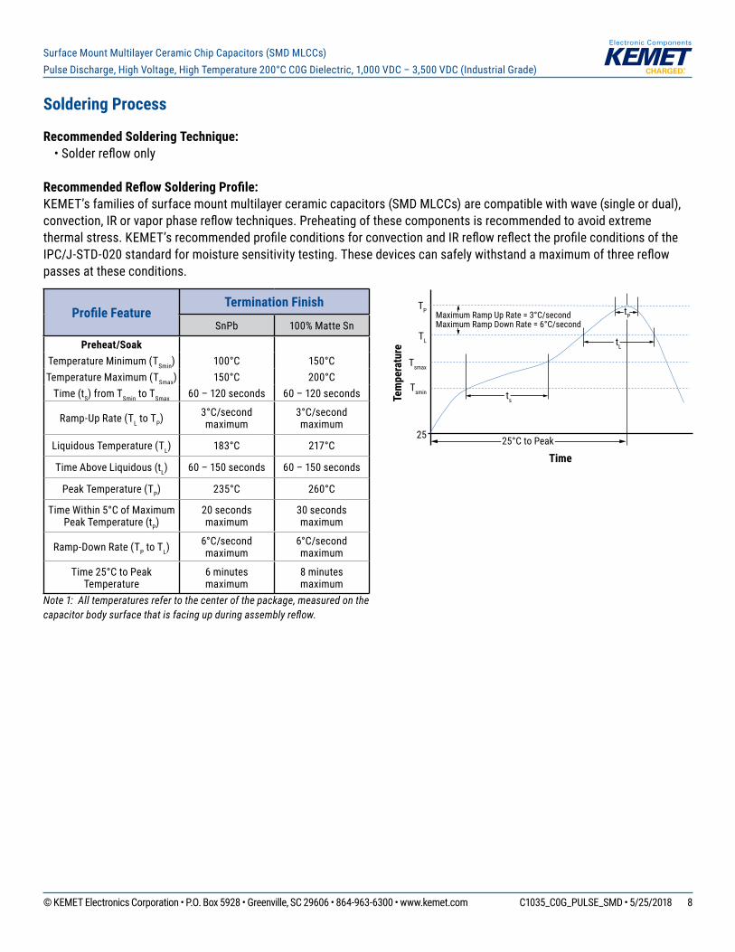
Soldering Process
Recommended Soldering Technique: • Solder reflow only
Recommended Reflow Soldering Profile:KEMET’s families of surface mount multilayer ceramic capacitors (SMD MLCCs) are compatible with wave (single or dual), convection, IR or vapor phase reflow techniques. Preheating of these components is recommended to avoid extreme thermal stress. KEMET’s recommended profile conditions for convection and IR reflow reflect the profile conditions of the IPC/J-STD-020 standard for moisture sensitivity testing. These devices can safely withstand a maximum of three reflow passes at these conditions.
Profile FeatureTermination Finish
SnPb 100% Matte Sn
Preheat/SoakTemperature Minimum (TSmin) 100°C 150°CTemperature Maximum (TSmax) 150°C 200°C
Time (tS) from TSmin to TSmax 60 – 120 seconds 60 – 120 seconds
Ramp-Up Rate (TL to TP) 3°C/second maximum
3°C/second maximum
Liquidous Temperature (TL) 183°C 217°C
Time Above Liquidous (tL) 60 – 150 seconds 60 – 150 seconds
Peak Temperature (TP) 235°C 260°C
Time Within 5°C of Maximum Peak Temperature (tP)
20 seconds maximum
30 seconds maximum
Ramp-Down Rate (TP to TL)6°C/second maximum
6°C/second maximum
Time 25°C to Peak Temperature
6 minutes maximum
8 minutes maximum
Note 1: All temperatures refer to the center of the package, measured on the capacitor body surface that is facing up during assembly reflow.
Time
Tem
pera
ture
Tsmin
25
Tsmax
TL
TP Maximum Ramp Up Rate = 3°C/secondMaximum Ramp Down Rate = 6°C/second
tP
tL
ts
25°C to Peak
© KEMET Electronics Corporation • P.O. Box 5928 • Greenville, SC 29606 • 864-963-6300 • www.kemet.com C1035_C0G_PULSE_SMD • 5/25/2018 9
Surface Mount Multilayer Ceramic Chip Capacitors (SMD MLCCs)Pulse Discharge, High Voltage, High Temperature 200°C C0G Dielectric, 1,000 VDC – 3,500 VDC (Industrial Grade)
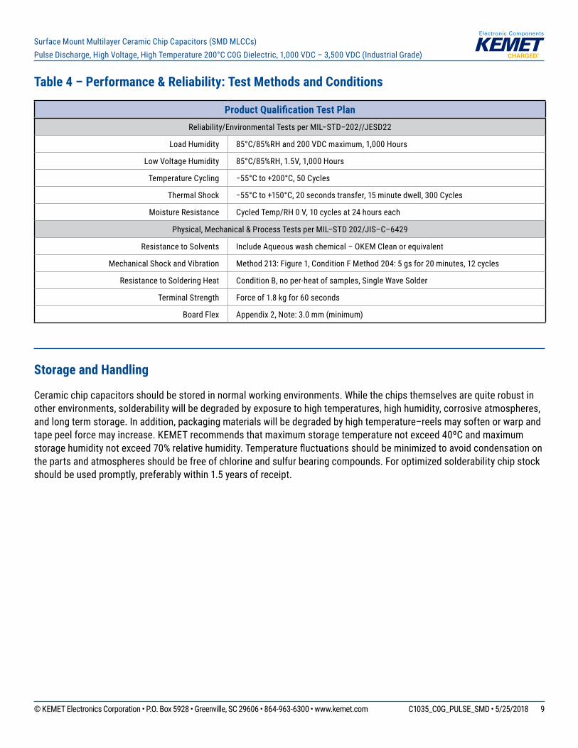
Table 4 – Performance & Reliability: Test Methods and Conditions
Product Qualification Test PlanReliability/Environmental Tests per MIL–STD–202//JESD22
Load Humidity 85°C/85%RH and 200 VDC maximum, 1,000 Hours
Low Voltage Humidity 85°C/85%RH, 1.5V, 1,000 Hours
Temperature Cycling −55°C to +200°C, 50 Cycles
Thermal Shock −55°C to +150°C, 20 seconds transfer, 15 minute dwell, 300 Cycles
Moisture Resistance Cycled Temp/RH 0 V, 10 cycles at 24 hours each
Physical, Mechanical & Process Tests per MIL–STD 202/JIS–C–6429
Resistance to Solvents Include Aqueous wash chemical – OKEM Clean or equivalent
Mechanical Shock and Vibration Method 213: Figure 1, Condition F Method 204: 5 gs for 20 minutes, 12 cycles
Resistance to Soldering Heat Condition B, no per-heat of samples, Single Wave Solder
Terminal Strength Force of 1.8 kg for 60 seconds
Board Flex Appendix 2, Note: 3.0 mm (minimum)
Storage and Handling
Ceramic chip capacitors should be stored in normal working environments. While the chips themselves are quite robust in other environments, solderability will be degraded by exposure to high temperatures, high humidity, corrosive atmospheres, and long term storage. In addition, packaging materials will be degraded by high temperature–reels may soften or warp and tape peel force may increase. KEMET recommends that maximum storage temperature not exceed 40ºC and maximum storage humidity not exceed 70% relative humidity. Temperature fluctuations should be minimized to avoid condensation on the parts and atmospheres should be free of chlorine and sulfur bearing compounds. For optimized solderability chip stock should be used promptly, preferably within 1.5 years of receipt.
© KEMET Electronics Corporation • P.O. Box 5928 • Greenville, SC 29606 • 864-963-6300 • www.kemet.com C1035_C0G_PULSE_SMD • 5/25/2018 10
Surface Mount Multilayer Ceramic Chip Capacitors (SMD MLCCs)Pulse Discharge, High Voltage, High Temperature 200°C C0G Dielectric, 1,000 VDC – 3,500 VDC (Industrial Grade)
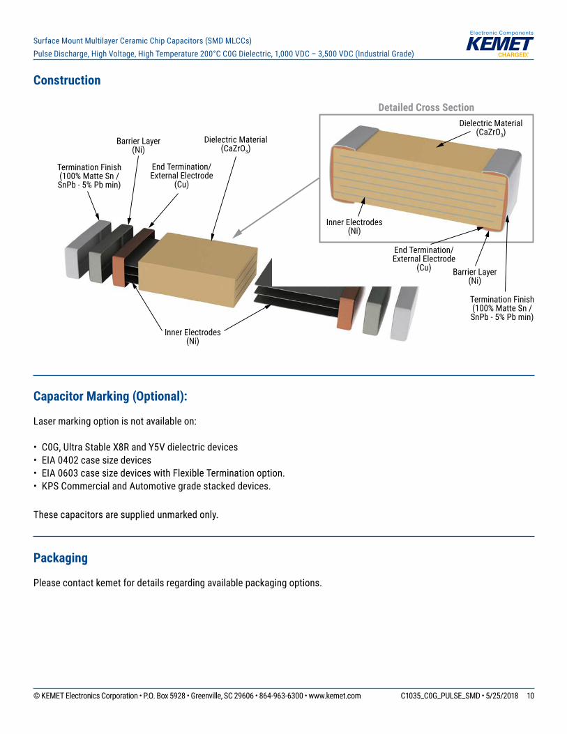
Construction
Detailed Cross Section
Barrier Layer(Ni)
Inner Electrodes(Ni)
Barrier Layer(Ni)
Inner Electrodes(Ni)
Dielectric Material(CaZrO3)Dielectric Material
(CaZrO3)
Termination Finish(100% Matte Sn / SnPb - 5% Pb min)
Termination Finish(100% Matte Sn / SnPb - 5% Pb min)
End Termination/External Electrode
(Cu)
End Termination/External Electrode
(Cu)
Capacitor Marking (Optional):
Laser marking option is not available on:
• C0G, Ultra Stable X8R and Y5V dielectric devices • EIA 0402 case size devices • EIA 0603 case size devices with Flexible Termination option.• KPS Commercial and Automotive grade stacked devices.
These capacitors are supplied unmarked only.
Packaging
Please contact kemet for details regarding available packaging options.
© KEMET Electronics Corporation • P.O. Box 5928 • Greenville, SC 29606 • 864-963-6300 • www.kemet.com C1035_C0G_PULSE_SMD • 5/25/2018 11
Surface Mount Multilayer Ceramic Chip Capacitors (SMD MLCCs)Pulse Discharge, High Voltage, High Temperature 200°C C0G Dielectric, 1,000 VDC – 3,500 VDC (Industrial Grade)
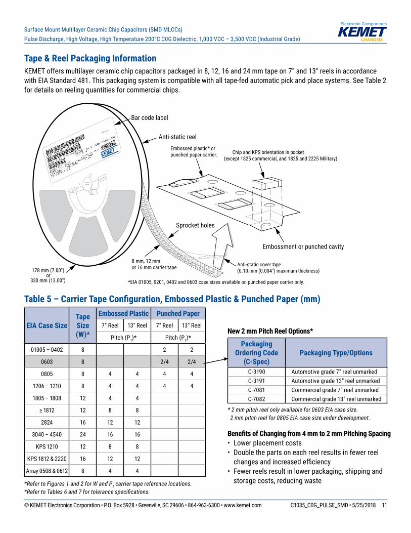
Tape & Reel Packaging InformationKEMET offers multilayer ceramic chip capacitors packaged in 8, 12, 16 and 24 mm tape on 7" and 13" reels in accordance with EIA Standard 481. This packaging system is compatible with all tape-fed automatic pick and place systems. See Table 2 for details on reeling quantities for commercial chips.
8 mm, 12 mmor 16 mm carrier tape 178 mm (7.00")
or330 mm (13.00")
Anti-static reel
Embossed plastic* or punched paper carrier.
Embossment or punched cavity
Anti-static cover tape(0.10 mm (0.004") maximum thickness)
Chip and KPS orientation in pocket(except 1825 commercial, and 1825 and 2225 Military)
*EIA 01005, 0201, 0402 and 0603 case sizes available on punched paper carrier only.
KEMET®
Bar code label
Sprocket holes
Table 5 – Carrier Tape Confi guration, Embossed Plastic & Punched Paper (mm)
EIA Case SizeTape Size (W)*
Embossed Plastic Punched Paper7" Reel 13" Reel 7" Reel 13" Reel
Pitch (P1)* Pitch (P1)*
01005 – 0402 8 2 2
0603 8 2/4 2/4
0805 8 4 4 4 4
1206 – 1210 8 4 4 4 4
1805 – 1808 12 4 4
≥ 1812 12 8 8
2824 16 12 12
3040 – 4540 24 16 16
KPS 1210 12 8 8
KPS 1812 & 2220 16 12 12
Array 0508 & 0612 8 4 4
*Refer to Figures 1 and 2 for W and P1 carrier tape reference locations.*Refer to Tables 6 and 7 for tolerance specifi cations.
New 2 mm Pitch Reel Options*
PackagingOrdering Code
(C-Spec)Packaging Type/Options
C-3190 Automotive grade 7" reel unmarkedC-3191 Automotive grade 13" reel unmarkedC-7081 Commercial grade 7" reel unmarkedC-7082 Commercial grade 13" reel unmarked
* 2 mm pitch reel only available for 0603 EIA case size. 2 mm pitch reel for 0805 EIA case size under development.
Benefi ts of Changing from 4 mm to 2 mm Pitching Spacing• Lower placement costs• Double the parts on each reel results in fewer reel
changes and increased effi ciency• Fewer reels result in lower packaging, shipping and
storage costs, reducing waste
© KEMET Electronics Corporation • P.O. Box 5928 • Greenville, SC 29606 • 864-963-6300 • www.kemet.com C1035_C0G_PULSE_SMD • 5/25/2018 12
Surface Mount Multilayer Ceramic Chip Capacitors (SMD MLCCs)Pulse Discharge, High Voltage, High Temperature 200°C C0G Dielectric, 1,000 VDC – 3,500 VDC (Industrial Grade)
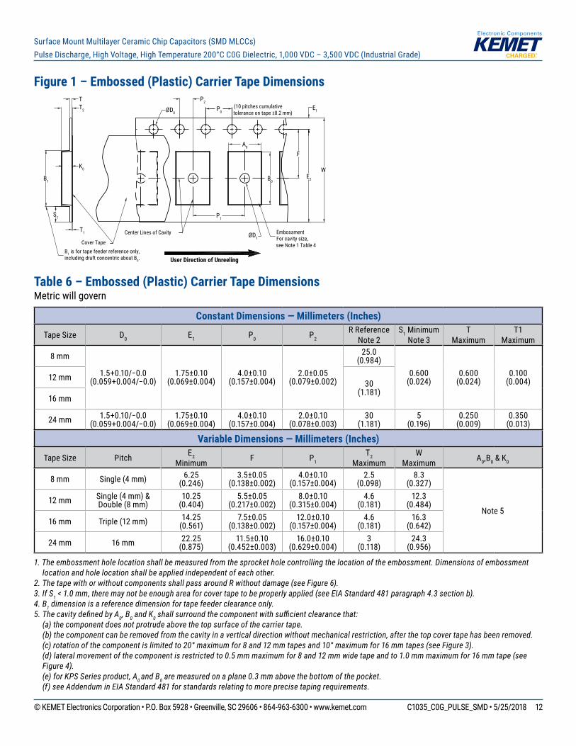
Figure 1 – Embossed (Plastic) Carrier Tape Dimensions
P0
T
F
W
Center Lines of Cavity
A0
B0
User Direction of Unreeling
Cover Tape
K0
B1 is for tape feeder reference only, including draft concentric about B0.
T2
ØD1
ØD0
B1
S1
T1
E1
E2
P1
P2
EmbossmentFor cavity size,see Note 1 Table 4
(10 pitches cumulativetolerance on tape ±0.2 mm)
Table 6 – Embossed (Plastic) Carrier Tape DimensionsMetric will govern
Constant Dimensions — Millimeters (Inches)
Tape Size D0 E1 P0 P2 R Reference
Note 2S1 Minimum
Note 3T
MaximumT1
Maximum
8 mm
1.5+0.10/−0.0(0.059+0.004/−0.0)
1.75±0.10(0.069±0.004)
4.0±0.10(0.157±0.004)
2.0±0.05(0.079±0.002)
25.0(0.984)
0.600(0.024)
0.600(0.024)
0.100(0.004)12 mm
30(1.181)
16 mm
24 mm 1.5+0.10/−0.0(0.059+0.004/−0.0)
1.75±0.10(0.069±0.004)
4.0±0.10(0.157±0.004)
2.0±0.10(0.078±0.003)
30(1.181)
5(0.196)
0.250(0.009)
0.350(0.013)
Variable Dimensions — Millimeters (Inches)
Tape Size Pitch E2Minimum F P1
T2Maximum
WMaximum A0,B0 & K0
8 mm Single (4 mm) 6.25(0.246)
3.5±0.05(0.138±0.002)
4.0±0.10(0.157±0.004)
2.5(0.098)
8.3(0.327)
Note 512 mm Single (4 mm) &
Double (8 mm)10.25
(0.404)5.5±0.05
(0.217±0.002)8.0±0.10
(0.315±0.004)4.6
(0.181)12.3
(0.484)
16 mm Triple (12 mm) 14.25(0.561)
7.5±0.05(0.138±0.002)
12.0±0.10(0.157±0.004)
4.6(0.181)
16.3(0.642)
24 mm 16 mm 22.25(0.875)
11.5±0.10(0.452±0.003)
16.0±0.10(0.629±0.004)
3(0.118)
24.3(0.956)
1. The embossment hole location shall be measured from the sprocket hole controlling the location of the embossment. Dimensions of embossment location and hole location shall be applied independent of each other.
2. The tape with or without components shall pass around R without damage (see Figure 6).3. If S1 < 1.0 mm, there may not be enough area for cover tape to be properly applied (see EIA Standard 481 paragraph 4.3 section b).4. B1 dimension is a reference dimension for tape feeder clearance only.5. The cavity defi ned by A0, B0 and K0 shall surround the component with suffi cient clearance that: (a) the component does not protrude above the top surface of the carrier tape. (b) the component can be removed from the cavity in a vertical direction without mechanical restriction, after the top cover tape has been removed. (c) rotation of the component is limited to 20° maximum for 8 and 12 mm tapes and 10° maximum for 16 mm tapes (see Figure 3). (d) lateral movement of the component is restricted to 0.5 mm maximum for 8 and 12 mm wide tape and to 1.0 mm maximum for 16 mm tape (see
Figure 4). (e) for KPS Series product, A0 and B0 are measured on a plane 0.3 mm above the bottom of the pocket. (f) see Addendum in EIA Standard 481 for standards relating to more precise taping requirements.
© KEMET Electronics Corporation • P.O. Box 5928 • Greenville, SC 29606 • 864-963-6300 • www.kemet.com C1035_C0G_PULSE_SMD • 5/25/2018 13
Surface Mount Multilayer Ceramic Chip Capacitors (SMD MLCCs)Pulse Discharge, High Voltage, High Temperature 200°C C0G Dielectric, 1,000 VDC – 3,500 VDC (Industrial Grade)
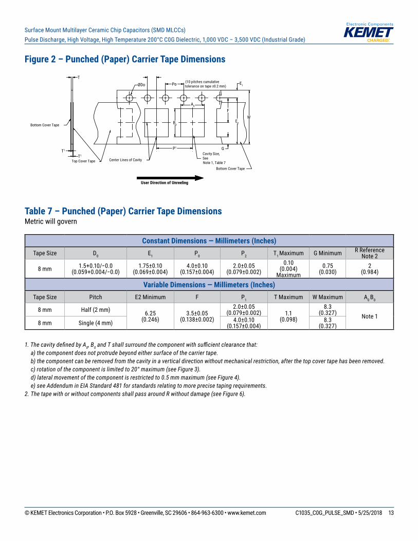
Figure 2 – Punched (Paper) Carrier Tape Dimensions
User Direction of Unreeling
Top Cover Tape
T
Center Lines of Cavity
P1
ØDo Po E1
F
E2
W
G
A0
B0
Cavity Size,SeeNote 1, Table 7
Bottom Cover Tape
T1
T1
Bottom Cover Tape
(10 pitches cumulativetolerance on tape ±0.2 mm)
Table 7 – Punched (Paper) Carrier Tape Dimensions Metric will govern
Constant Dimensions — Millimeters (Inches)Tape Size D0 E1 P0 P2 T1 Maximum G Minimum R Reference
Note 2
8 mm 1.5+0.10/−0.0(0.059+0.004/−0.0)
1.75±0.10(0.069±0.004)
4.0±0.10(0.157±0.004)
2.0±0.05(0.079±0.002)
0.10(0.004)
Maximum0.75
(0.030) 2
(0.984)
Variable Dimensions — Millimeters (Inches)Tape Size Pitch E2 Minimum F P1 T Maximum W Maximum A0 B0
8 mm Half (2 mm) 6.25(0.246)
3.5±0.05(0.138±0.002)
2.0±0.05(0.079±0.002) 1.1
(0.098)
8.3(0.327) Note 1
8 mm Single (4 mm) 4.0±0.10(0.157±0.004)
8.3(0.327)
1. The cavity defi ned by A0, B0 and T shall surround the component with suffi cient clearance that: a) the component does not protrude beyond either surface of the carrier tape. b) the component can be removed from the cavity in a vertical direction without mechanical restriction, after the top cover tape has been removed. c) rotation of the component is limited to 20° maximum (see Figure 3). d) lateral movement of the component is restricted to 0.5 mm maximum (see Figure 4). e) see Addendum in EIA Standard 481 for standards relating to more precise taping requirements.2. The tape with or without components shall pass around R without damage (see Figure 6).
© KEMET Electronics Corporation • P.O. Box 5928 • Greenville, SC 29606 • 864-963-6300 • www.kemet.com C1035_C0G_PULSE_SMD • 5/25/2018 14
Surface Mount Multilayer Ceramic Chip Capacitors (SMD MLCCs)Pulse Discharge, High Voltage, High Temperature 200°C C0G Dielectric, 1,000 VDC – 3,500 VDC (Industrial Grade)
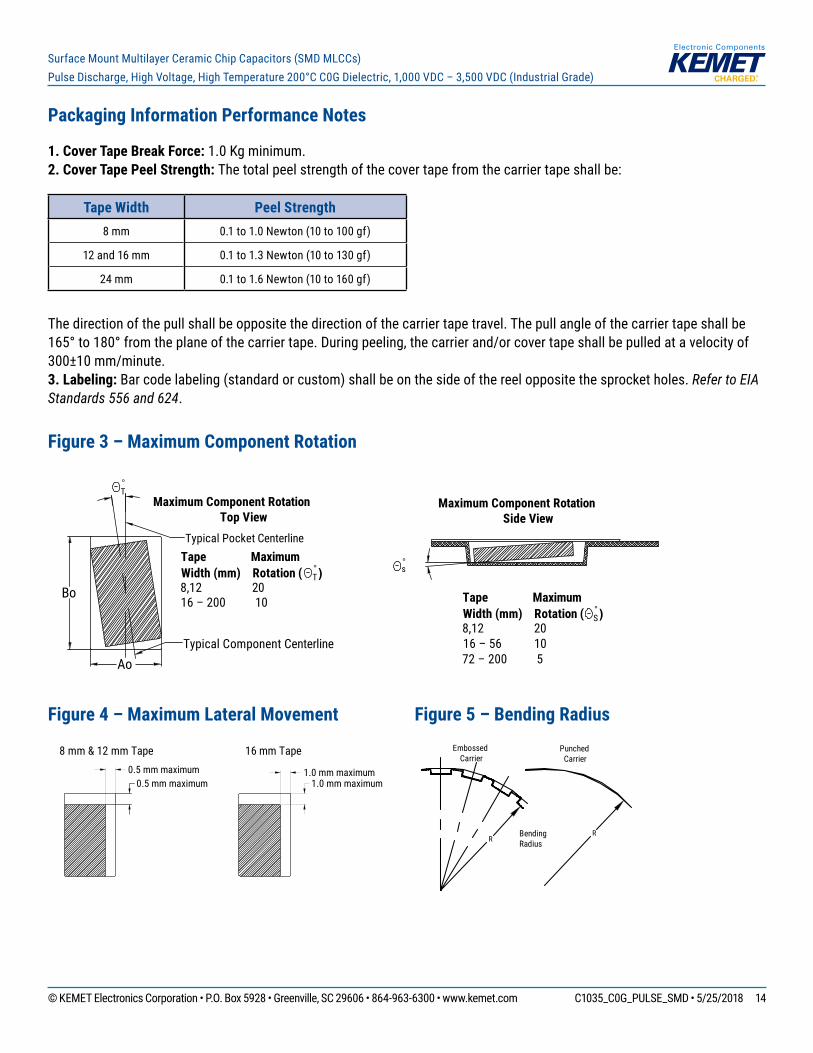
Packaging Information Performance Notes
1. Cover Tape Break Force: 1.0 Kg minimum.2. Cover Tape Peel Strength: The total peel strength of the cover tape from the carrier tape shall be:
Tape Width Peel Strength8 mm 0.1 to 1.0 Newton (10 to 100 gf)
12 and 16 mm 0.1 to 1.3 Newton (10 to 130 gf)
24 mm 0.1 to 1.6 Newton (10 to 160 gf)
The direction of the pull shall be opposite the direction of the carrier tape travel. The pull angle of the carrier tape shall be 165° to 180° from the plane of the carrier tape. During peeling, the carrier and/or cover tape shall be pulled at a velocity of 300±10 mm/minute.3. Labeling: Bar code labeling (standard or custom) shall be on the side of the reel opposite the sprocket holes. Refer to EIA Standards 556 and 624.
Figure 3 – Maximum Component Rotation
Ao
Bo
°T
°s
Maximum Component RotationTop View
Maximum Component RotationSide View
Tape MaximumWidth (mm) Rotation ( °
T)8,12 20 16 – 200 10 Tape Maximum
Width (mm) Rotation ( °S)
8,12 20 16 – 56 1072 – 200 5
Typical Pocket Centerline
Typical Component Centerline
Figure 4 – Maximum Lateral Movement
0.5 mm maximum0.5 mm maximum
8 mm & 12 mm Tape
1.0 mm maximum1.0 mm maximum
16 mm Tape
Figure 5 – Bending Radius
RRBending
Radius
EmbossedCarrier
PunchedCarrier
© KEMET Electronics Corporation • P.O. Box 5928 • Greenville, SC 29606 • 864-963-6300 • www.kemet.com C1035_C0G_PULSE_SMD • 5/25/2018 15
Surface Mount Multilayer Ceramic Chip Capacitors (SMD MLCCs)Pulse Discharge, High Voltage, High Temperature 200°C C0G Dielectric, 1,000 VDC – 3,500 VDC (Industrial Grade)
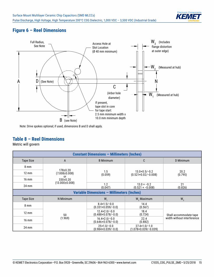
Figure 6 – Reel Dimensions
A D (See Note)
Full Radius,See Note
B (see Note)
Access Hole atSlot Location(Ø 40 mm minimum)
If present,tape slot in corefor tape start:2.5 mm minimum width x10.0 mm minimum depth
W3 (Includes flange distortion at outer edge)
W2 (Measured at hub)
W1 (Measured at hub)
C(Arbor holediameter)
Note: Drive spokes optional; if used, dimensions B and D shall apply.
N
Table 8 – Reel DimensionsMetric will govern
Constant Dimensions — Millimeters (Inches) Tape Size A B Minimum C D Minimum
8 mm178±0.20
(7.008±0.008) or
330±0.20(13.000±0.008)
1.5 (0.059)
13.0+0.5/−0.2 (0.521+0.02/−0.008)
20.2 (0.795)12 mm
16 mm
24 mm 1.2(0.047)
13.0 + −0.2 (0.521 + −0.008)
21(0.826)
Variable Dimensions — Millimeters (Inches) Tape Size N Minimum W1 W2 Maximum W3
8 mm
50 (1.969)
8.4+1.5/−0.0(0.331+0.059/−0.0)
14.4 (0.567)
Shall accommodate tape width without interference
12 mm 12.4+2.0/−0.0(0.488+0.078/−0.0)
18.4 (0.724)
16 mm 16.4+2.0/−0.0(0.646+0.078/−0.0)
22.4 (0.882)
24 mm 25+1.0/−0.0(0.984+0.039/−0.0)
27.4+1.0/−1.0(1.078+0.039/−0.039)
© KEMET Electronics Corporation • P.O. Box 5928 • Greenville, SC 29606 • 864-963-6300 • www.kemet.com C1035_C0G_PULSE_SMD • 5/25/2018 16
Surface Mount Multilayer Ceramic Chip Capacitors (SMD MLCCs)Pulse Discharge, High Voltage, High Temperature 200°C C0G Dielectric, 1,000 VDC – 3,500 VDC (Industrial Grade)
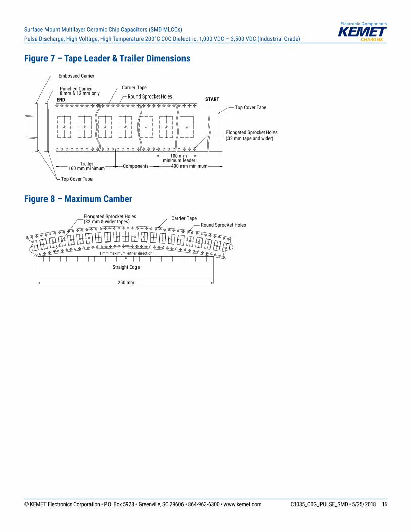
Figure 7 – Tape Leader & Trailer Dimensions
Trailer160 mm minimum
Carrier Tape
END STARTRound Sprocket Holes
Elongated Sprocket Holes(32 mm tape and wider)
Top Cover Tape
Top Cover Tape
Punched Carrier8 mm & 12 mm only
Embossed Carrier
Components
100 mm minimum leader
400 mm minimum
Figure 8 – Maximum Camber
Carrier TapeRound Sprocket Holes
1 mm maximum, either direction
Straight Edge
250 mm
Elongated Sprocket Holes(32 mm & wider tapes)
© KEMET Electronics Corporation • P.O. Box 5928 • Greenville, SC 29606 • 864-963-6300 • www.kemet.com C1035_C0G_PULSE_SMD • 5/25/2018 17
Surface Mount Multilayer Ceramic Chip Capacitors (SMD MLCCs)Pulse Discharge, High Voltage, High Temperature 200°C C0G Dielectric, 1,000 VDC – 3,500 VDC (Industrial Grade)
KEMET Electronics Corporation Sales Offi ces
For a complete list of our global sales offi ces, please visit www.kemet.com/sales.
DisclaimerAll product specifi cations, statements, information and data (collectively, the “Information”) in this datasheet are subject to change. The customer is responsible for checking and verifying the extent to which the Information contained in this publication is applicable to an order at the time the order is placed.
All Information given herein is believed to be accurate and reliable, but it is presented without guarantee, warranty, or responsibility of any kind, expressed or implied.
Statements of suitability for certain applications are based on KEMET Electronics Corporation’s (“KEMET”) knowledge of typical operating conditions for such applications, but are not intended to constitute – and KEMET specifi cally disclaims – any warranty concerning suitability for a specifi c customer application or use. The Information is intended for use only by customers who have the requisite experience and capability to determine the correct products for their application. Any technical advice inferred from this Information or otherwise provided by KEMET with reference to the use of KEMET’s products is given gratis, and KEMET assumes no obligation or liability for the advice given or results obtained.
Although KEMET designs and manufactures its products to the most stringent quality and safety standards, given the current state of the art, isolated component failures may still occur. Accordingly, customer applications which require a high degree of reliability or safety should employ suitable designs or other safeguards (such as installation of protective circuitry or redundancies) in order to ensure that the failure of an electrical component does not result in a risk of personal injury or property damage.
Although all product–related warnings, cautions and notes must be observed, the customer should not assume that all safety measures are indicted or that other measures may not be required.
KEMET is a registered trademark of KEMET Electronics Corporation.