Embed Size (px)
Citation preview

SURFACE-MODIFIED FERRITIC INTERCONNECT MATERIALS FOR SOLID OXIDE FUEL CELLS
FINAL REPORT SwRI® Project No. 18.06195
DE-FC26-O2NT41579
Reporting Period 10/01/02 through 12/31/03
Prepared for U.S. Department of Energy
National Energy Technology Laboratory Pittsburgh, PA 15236-0940
Prepared by Bruce R. Lanning, Ph.D.
James Arps, Ph.D. Ronghua Wei, Ph.D.
Goeff Dearnaley, Ph.D.
Phone (210) 522-2934 Fax (210) 522-6220
e-mail [email protected]
Southwest Research Institute 6220 Culebra Road
San Antonio, TX 78238
March 15, 2004 S O U T H W E S T R E S E A R C H I N S T I T U T E
SAN ANTONIO HOUSTON WASHINGTON, DC

SURFACE-MODIFIED FERRITIC INTERCONNECT MATERIALS FOR SOLID OXIDE FUEL CELLS
FINAL REPORT SwRI® Project No. 18.06195
DE-FC26-O2NT41579
Reporting Period 10/01/02 through 12/31/03
Prepared for U.S. Department of Energy
National Energy Technology Laboratory Pittsburgh, PA 15236-0940
Prepared by Bruce R. Lanning, Ph.D.
James Arps, Ph.D. Ronghua Wei, Ph.D.
Goeff Dearnaley, Ph.D.
Phone (210) 522-2934 Fax (210) 522-6220
e-mail [email protected]
Southwest Research Institute 6220 Culebra Road
San Antonio, TX 78238
March 15, 2004 APPROVED: ______________________________ James Lankford, Ph.D., Director
Materials Engineering Department

DISCLAIMER
This report was prepared as an account of work sponsored by an agency of the United States Government. Neither the United States Government nor any agency thereof, nor any of their employees, makes any warranty, express or implied, or assumes any legal liability or responsibility for the accuracy, completeness, or usefulness of any information, apparatus, product, or process disclosed, or represents that its use would not infringe privately owned rights. Reference herein to any specific commercial product, process, or service by trade name, trademark, manufacturer, or otherwise does not necessarily constitute or imply its endorsement, recommendation, or favoring by the United States Government or any agency thereof. The views and opinions of authors expressed herein do not necessarily state or reflect those of the United States Government or any agency thereof.

ABSTRACT
Interconnects are a critical element of an SOFC assembly and although much work has
focused on chromium and chromium-iron alloys containing an oxide that is both oxidation resistant and electrically conductive, the thermal instability of typical native metal oxides allow interdiffusion of cations across the interconnect-electrode boundary that ultimately leads to degradation of SOFC performance. Phase I of the SECA Core Technology Program has been a one-year effort to investigate and evaluate the feasibility of: 1) Ion implanting an alumina-scale forming ferritic steel, such as FeCrAlY, to form an interconnect material with low resistance (< 0.1 Ω/cm2) in oxidizing/reducing environments up to 800oC, and 2) Maintaining the above low resistance metric for an extended time (> 1000 hours at 800oC) in contact with an LSF cathode material.
We confirmed, as part of our oxidation kinetics evaluation of FeCrAlY and 430 ferritic steel, the parabolic growth of a mixed chromia/alumina scale on FeCrAlY and a single chromia layer in the case of the 430 stainless steel; the outer contiguous layer of Al2O3, in the case of FeCrAlY, forming a stable, self-limiting, protective scale with no detectable cation interdiffusion between FeCrAlY and an LSF electrode even after 1000 hours at 800°C in air. To render the alumina scale conductive, we implanted either titanium or niobium ions into FeCrAlY scales to a fixed depth (0.12 µm), varying only the thickness of the oxide. ASR for an un-doped FeCrAlY oxide scale (i.e., alumina) was more than an order of magnitude greater than the 430 control sample whereas, the ASR for the doped FeCrAlY oxide scale sample was comparable to the 430 control sample; hence, the resistance of a doped alumina scale on FeCrAlY was equal to the resistance of a chromia-scale forming alloy, such as 430 (chromia scales of which are typically < 0.1 Ω-cm).
Along with the ASR measurements, AC impedance measurements were conducted to evaluate conduction mechanisms. From the AC impedance measurements, we observed that the addition of niobium resulted in at least a two order of magnitude reduction in resistance over the un-doped specimen and that the conduction in the doped alumina scale was pure electronic conduction, as opposed to mixed ionic-electronic conduction (dominated by intrinsic (ionic) defects) for the un-doped alumina scales. The DC resistance component was ~ 4 Ω although when this value is adjusted to account for the system resistance (i.e., leads, junctions, etc.), the ASR was determined to be < 0.1 Ω-cm; even after 1000 hours at 800°C in air.
Our results have clearly shown that dopant additions increase the electronic conductivity of alumina forming scale alloys, such as FeCrAlY, transforming from a mixed ionic/electronic conduction mechanism. Just as importantly, the demonstrated stable formation of an alumina scale was shown to be an advantage over conventional pure chromia forming alloys as interconnect materials.
i

TABLE OF CONTENTS
Page
ABSTRACT......................................................................................................................... i 1.0 INTRODUCTION..................................................................................................... 1 1.1 Technical Need/Issues Addressed.............................................................. 1 1.2 Technical Approach..................................................................................... 1 1.3 Program Objectives..................................................................................... 2 2.0 EXECUTIVE SUMMARY ........................................................................................ 3 3.0 EXPERIMENTAL .................................................................................................... 4 3.1 Specimen Preparation................................................................................. 4 3.2 Oxidation ..................................................................................................... 5 3.3 Small-area Ion Implantation ........................................................................ 5 3.4 Electrical Measurements (ASR/AC Impedance).......................................... 6 3.5 Interconnect/Cathode Diffusion Couple....................................................... 9 4.0 RESULTS/DISCUSSION ........................................................................................ 10 4.1 Pre-oxidation Behavior (Kinetics) of Alumina-forming Scales on FeCrAlY.. 10 4.2 Scale Resistance Measurements ................................................................ 13 4.2.1 ASR Measurements......................................................................... 13 4.2.2 AC Impedance Measurement .......................................................... 16 4.3 Long Term Testing of Interconnect/LSF Cathode Materials at 800°C......... 20 4.4 Large Area Ion Source Development .......................................................... 22 4.4.1 Introduction (PII and PIIP) ............................................................... 23 4.4.2 Metal Plasma Source Design .......................................................... 24 5.0 CONCLUSIONS...................................................................................................... 27 6.0 REFERENCES........................................................................................................ 28 7.0 ACKNOWLEDGEMENTS ....................................................................................... 28
LIST OF TABLE Table Page
1 Composition of Alloys Used in this Study ..................................................... 4
ii

LIST OF FIGURES Figure Page
1 AES of Nb-implanted FeCrAlY scale at 0.09 µm depth. Scale growth conditions: 900°C in air for 2 hours (~ 0.15 µm-thick oxide). .......................
5
2 Schematic of contacting configurations for high-temperature resistance
measurements. ...................................................................................................
6
3 Load Fixture and corresponding test station for high temperature DC and AC Impedance Measurements. ........................................................................
7
4 Verification of linear resistance behavior at different temperatures. ............ 7
5 AC impedance plots for un-doped FeCrAlY @ 900°C for different exposure times....................................................................................................
8
6 Verification of Ohm’s law at different temperatures............................................... 9
7 Weight gain of FeCrAlY and 430 stainless steels at 900°C in dry air. ......... 10
8 Parabolic rate constants for oxide growth on FeCrAlY alloy in dry air......... 11
9 X-ray diffraction patterns of the oxide scale thermally grown on the surface of FeCrAlY at different temperatures. ................................................
12
10 AES depth profile of thermally grown oxide scale in air (2 hr. @ 900oC)
on FeCrAlY. ................................................................................................
12
11 Comparison of ASR of un-doped FeCrAlY scale (thermally grown at 950oC for 24 hours) with platinum paste electrodes at different exposure times............................................................................................
13
12 Comparison of ASR of niobium-doped (scales of various thicknesses), un-doped, FeCrAlY alloy scales, and 430 stainless steel with platinum paste electrodes; exposure times greater than 24 hours.. ..........................
14
13 Comparison of ASR of titanium-doped (scales of various thicknesses) and un-doped, FeCrAlY alloy scales with platinum paste electrodes..........
15
14 AC impedance response of un-doped FeCrAlY as a function of
temperature (platinum paste contact). ........................................................
17
15 AC impedance response of un-doped FeCrAlY alloy during cool-down (platinum paste contact)..............................................................................
18
iii
LIST OF FIGURES (Continued) Figure Page
16 AC impedance response of niobium-doped FeCrAlY scale, 0.15 µm-thick as a function of temperature (platinum paste contact). ...............................
18
17 AC impedance plot for un-doped and Nb-doped FeCrAlY alumina scales
after 1000 hours at 800oC in air; enlarged view around origin shown by inset. ...........................................................................................................
19
18 AC impedance response for titanium-doped FeCrAlY alloy as a function of temperature (platinum paste contact). ....................................................
19
19 LSF/FeCrALY contact @800oC for 1000 hours (intimate contact); SEM
and X-ray dot maps for: a) SEM, b) aluminum, c) oxygen, d) lanthanum, e) chromium, f) iron.....................................................................................
21
20 LSF/FeCrAlY contact @800oC for 1000 hours (slight gap); SEM and X-ray dot maps for: a) SEM, b) aluminum, c) oxygen, d) lanthanum, e) strontium, and f) iron...............................................................................
22
21 Comparison of ion beam processing and plasma processing. .................... 23
22 Schematic and mechanical of the metal ion source for plasma processing. .................................................................................................
24
23 Schematic of the MPIII and MPIIP system.................................................. 25
24 (a) Mechanical design, and (b) physical structure of the metal plasma source. ........................................................................................................
26
25 Metal plasma source with (a) discharge chamber, and (b) with solenoid
(fully assembled).........................................................................................
26
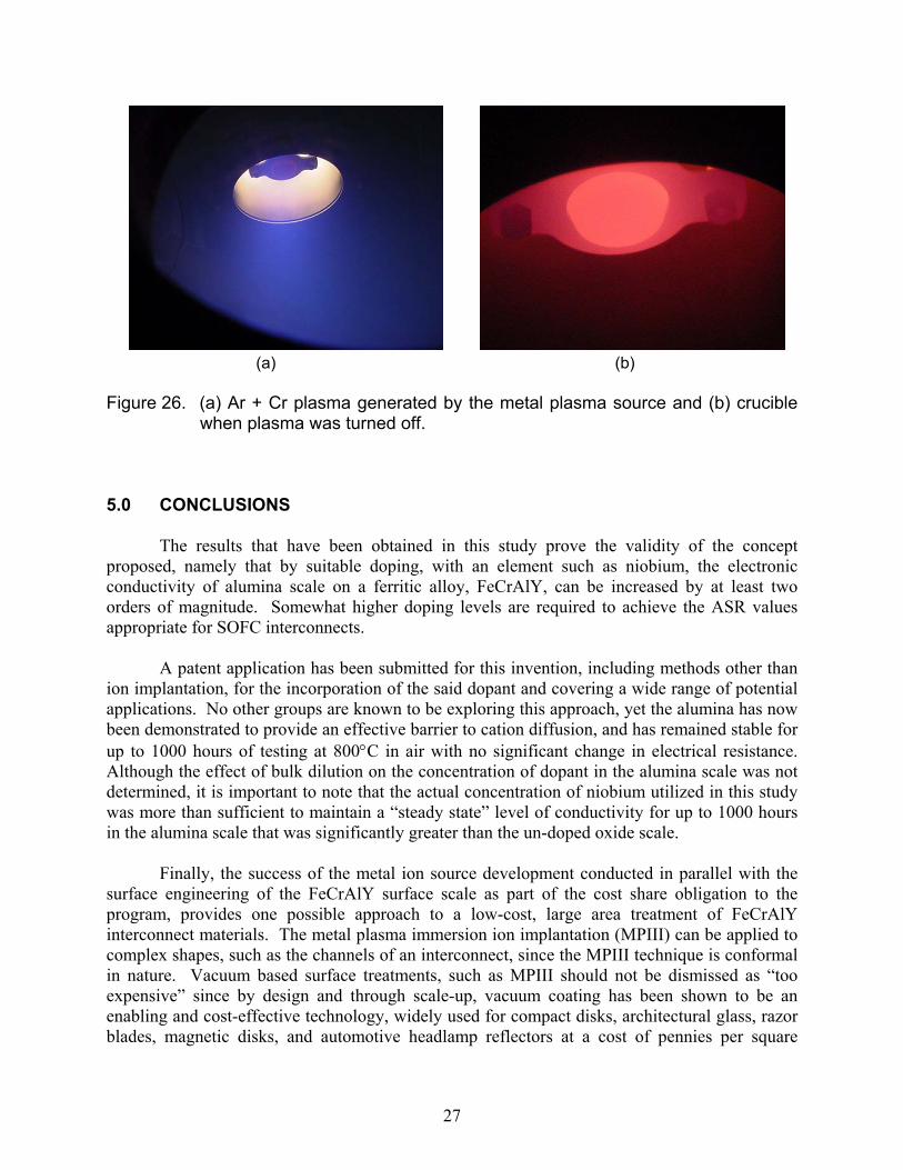
26 (a) Ar + Cr plasma generated by the metal plasma source and (b) crucible when plasma was turned off. .........................................................
27
iv

1.0 INTRODUCTION 1.1 Technical Needs/Issues Addressed
As the trend in planar SOFC development is driven to lower temperatures (i.e., <800oC), oxidation-resistant metal alloys become feasible as candidate interconnect materials. Although much work has focused on metal alloys for interconnect materials and in particular chromium alloys containing an oxide that is both oxidation resistant and electrically conductive, the thermal instability of typical native metal oxides allow interdiffusion of cations across the interconnect-electrode boundary that ultimately leads to degradation of SOFC performance. The instability, in the case of chromium alloys, is due in part to the volatile nature of the chromium oxide in combination with the outward migration of highly mobile chromium cations in the process of oxidation. In brief, the continued growth of chromia-forming scales at high temperatures leads to spallation and instability at the interconnect-electrode boundary. 1.2 Technical Approach
Realizing that without taking the first step of establishing a stable oxide at the electrode/interconnect interface or boundary, SOFC cell performance will be severely constrained as the cell resistance will continue to increase during repeated thermal cycling and sustained use at high temperature. For protection in oxidizing environments, interconnect metals must develop a surface scale that is slow-growing, adherent, and will serve as a diffusion barrier between the oxidant and the underlying alloy. Although alloying has been used to improve resistance of surface oxide scales, this comes at the expense of mechanical durability. Similarly, coatings can be applied to increase resistance, although oxidants can often easily permeate through the coatings and the parent material ultimately relies on its own scale for protection.
Since ferritic steels are well matched in expansion coefficients to the ceramic elements of an SOFC cell, the challenge for use of these materials at high temperatures is the formation of a stable scale in light of the chromia-forming tendencies of the ferritic (high chrome) alloy matrix. Formation of chromia scales at the interconnect-electrode boundary has been shown to degrade SOFC performance due in part to the volatile nature of the chromium oxide in combination with the outward migration of a highly mobile chromium cation in the process of oxidation affecting cathode performance.
The addition of rare earth elements, on the other hand, in alumina or chromia-forming alloys is known to stabilize surface scales as a result of the higher affinity for oxygen (as well as other impurity elements such as sulfur) of the scale-forming component; i.e., yttrium, for example, is known to preferentially migrate to the surface in ferritic alloys, reducing cation mobility as it accumulates, also, along grain boundaries. Reactive elements at the surface can reduce growth rates, increase scale adherence, and even change the transport mechanisms through the scale from predominantly metal transport outward to oxygen transport inward. They produce a smother, finer-grained scale.
To address the issue of thermal stability of a metal alloy for use in oxidizing/reducing environments at elevated temperatures, our approach was to first use a material that had prior
1

service history in these environments; namely, FeCrAlY, an alloy that was developed as a cladding material for fuel elements in an Advanced Gas-Cooled Reactor (AGR) project conducted in the U.K. The alloy has been shown to withstand temperatures up to 950oC in a mixture of carbon dioxide, carbon monoxide and methane for very extended periods (typically over 40,000 hours) and thousands of thermal cycles without spallation since any formation of a weakly bound radioactive oxide would have created major problems in the coolant loop. Similarly, this general class of alloy has also been successfully and extensively used as a bond coat layer as part of a thermal barrier coating system on turbine blades and the thermodynamic and kinetic behavior of FeCrAlY in this thermally demanding, “sandwich-type” structure, analogous to the layered SOFC flat plate structure, is well documented.
Although the high-temperature stability of the yttrium-containing alumina oxide on FeCrAlY is well established, the thin oxide scale does not provide sufficient electronic conductivity at 800oC and it is this challenge of rendering the native oxide electronically conductive at 800oC that was the basis for the second component of our approach. For comparison, the electronic conductivity of Cr2O3 at 900°C is 10-3 to 10-2 S cm-1 and that of lanthanum chromite is similar. However, Dearnaley and Goode have shown [1] that the conductivity of alumina can be raised by many orders of magnitude, even at room temperature, by the ion implantation of selected quadrivalent dopants such as tin or lead. It is not known whether these act as donors within the lattice or by segregation to form conductive oxides. In the latter case, it is likely that the dual implantation of indium and tin into a thin film of alumina would be even more effective in reducing the electrical resistivity. Conductivities as great as 10-2 to 10-1 S cm–1 have been measured in lead-implanted polycrystalline alumina at room temperature at dopant concentrations of a few atomic percent [2]. Additionally, ion implantation has been shown to increase, strongly, the electrical conductivity of rutile and MgO, and other types of insulating metal oxides [3,4]. Based on these reported results in the literature, the second aspect of our approach was to implant candidate ions at dosages of a few atomic percent into the surface (100-150 nm) of a pre-conditioned FeCrAlY alloy in order to reduce the high-temperature resistance. 1.3 Program Objectives
Phase I of the SECA Core Technology Program has been a one-year effort to investigate and evaluate the feasibility of the following specific objectives:
1. Engineer a surface oxide scale on a ferritic stainless steel that is: a. Mechanically and chemically stable at 800°C in oxidizing and reducing
environments, and b. Electrically conductive to minimize stack IR losses.
2. Develop/implement treatment process for rendering the alumina scale electrically conductive (such as metal ion implantation) that is inherently scaleable for manufacturing.
3. Demonstrate stable electrical conductivity of interconnects for an extended time (> 1000 hours) at 800°C in contact with cathode materials ((La0.8Sr0.2)FeO3 and (La0.6Sr0.4)(Fe0.8Co0.2)O3).
2

2.0 EXECUTIVE SUMMARY
Interconnects are a critical element of an SOFC assembly in that they must: (1) be easily formable and machinable, (2) be thermally matched to adjoining ceramic cell components, (3) have mechanical integrity and fracture toughness over prolonged periods of exposure to high temperature, reducing/oxidizing environments, and (4) develop surface scales that are not only stable and electrically conductive over a large O2 concentration range, but prevent ion migration or gas permeation across the interconnect-electrode boundary. Although much work has focused on metal alloys for interconnect materials and in particular chromium alloys containing an oxide that is both oxidation resistant and electrically conductive, the thermal instability of typical native metal oxides allow interdiffusion of cations across the interconnect-electrode boundary that ultimately leads to degradation of SOFC performance.
Phase I of the SECA Core Technology Program has been a one-year effort to investigate and evaluate the feasibility of:
1. Ion implanting an alumina-scale forming ferritic steel, such as FeCrAlY, to form an interconnect material with low resistance (< 0.1 Ω/cm2) in oxidizing/reducing environments up to 800°C, and
2. Maintaining the above low resistance metric for an extended time (> 1000 hours
at 800°C) in contact with an LSF cathode material.
We confirmed, as part of our oxidation kinetics evaluation of FeCrAlY and 430 much thicker steel, the parabolic growth of a mixed chromia/alumina scale on FeCrAlY and a single chromia layer in the case of the 430 stainless steel; the outer contiguous layer of Al2O3, in the case of FeCrAlY, forming a stable, self-limiting, protective scale. To render the alumina scale conductive, we then implanted either titanium or niobium ions into FeCrAlY scales to a fixed depth, varying only the thickness of the oxide. Area Specific Resistance (ASR) was measured as a function of temperature and time at temperature using both a modified 4-point DC and AC impedance techniques.
As a result of the relatively high lead/system resistance component of the overall ASR measurement, a consequence of the test configuration, a qualitative measurement of the DC resistance was obtained, using an oxidized 430 SS specimen as a means for comparison. ASR for an un-doped FeCrAlY oxide scale (i.e., alumina) was more than an order of magnitude greater than the 430 control sample whereas, the ASR for the doped FeCrAlY oxide scale sample was comparable to the 430 control sample; hence, the resistance of a doped alumina scale on FeCrAlY was found to be equal to the resistance of a chromia-scale forming alloy, such as 430 (typically < 0.1 Ω-cm).
Along with the DC ASR measurements, AC impedance measurements were used to assess basic conduction mechanisms across the various interfaces of the contact up to 800°C, providing confirmation of the effect of the dopant. Based on the AC impedance results, un-doped alumina scales exhibited mixed conduction and the transport limited mechanisms of a high impedance, solid state electrolyte. Addition of niobium resulted in at least a two order of
3

magnitude reduction in resistance over the un-doped specimen, resulted in pure electronic conduction, as opposed to mixed ionic-electronic conduction, even after 1000 hours at 800°C (DC resistance component was less than the system resistance (i.e., leads, junctions, etc.).
A diffusion couple experiment, placing a doped FeCrAlY alumina scale in contact with an LSF cathode material for 1000 hours at 800°C confirmed the stability of the interface region. No detectable cation interdiffusion took place across the contiguous alumina layer and thickness of the scale layer remained essentially unchanged after 500 hours at temperature. This stability of the alumina scale on FeCrAlY is consistent with its reported long-term stability (~ 40,000 hours at 950°C) in Advanced Gas Cooled Reactors for the nuclear industry.
Our results have clearly shown that dopant additions increase the electronic conductivity of alumina forming scale alloys, such as FeCrAlY, transforming from a mixed ionic/electronic conduction mechanism. Just as importantly, the demonstrated stable formation of an alumina scale is a clear advantage over conventional pure chromia forming alloys for interconnect materials. Future work in this area would be to optimize the dopant addition/concentration and any possible effects of bulk dilution (although none were observed in the limited 1000 hour tests of this study), as well as the type of dopant addition; i.e., strontium and TiO2 as opposed to pure titanium. Since we have proved the concept of this procedure (patent application submitted) the next step would be to develop more scaleable manufacturing processes that achieve the same oxide composition, e.g., by magnetron sputtering, sol-gel or other similar processes. 3.0 EXPERIMENTAL 3.1 Specimen Preparation
Two commercial alloys were tested in this study, FeCrAlY, 0.05 mm foil and 5 mm sheet from Goodfellow, and stainless steel type 430 from Allegheny Ludlum (3 mil thick). The compositions of these two alloys are shown in Table 1 below.
Table 1. Composition of Alloys Used in this Study
Composition Alloy
Fe Cr Al Si Y C Mn Mo P S
FeCrAlY Bal.
(72.6) 22 4.8 0.3 0.3
430 (UNS43000) Bal. 16-18 1.0* 0.12* 1.0* 0.5* 0.04* 0.03*
* Note: Refers to maximum concentration.
4

All samples were either sheared or milled into 1 cm × 1 cm squares and for the oxide growth experiments in air, a small hole was drilled in one corner to suspend the samples. Prior to oxidation, samples were polished on both faces with 1200 grit paper, ultrasonically cleaned in acetone, and rinsed with methanol. 3.2 Oxidation
Alloy specimens, after polishing, were tested at different temperatures under different atmospheres; specimens were suspended in a tube furnace through which air or humidified air (purged in H2O bath) was flowed across the specimen surface at elevated temperatures (700 - 1100°C). Specimens were exposed for specific durations (up to 24 hours) at the test temperatures, removed, and then allowed to air quench outside the furnace. Weight change was determined with a micro-balance. 3.3 Small-area Ion Implantation
FeCrAlY test coupons (1 cm x 1 cm x 0.5 cm-thick) were first polished and then annealed in air at temperatures greater than 850oC to grow oxides of three different thicknesses, 0.15 µm, 0.3 µm, and 0.6 µm. Along with an un-oxidized control sample, the three samples were then implanted with niobium and titanium ions at energies of 280 and 150 keV, respectively. Nominal penetration depth was 0.12 µm and the ion dose was 1 × 10¹⁶ atoms/cm2. Niobium penetration depth was confirmed by Auger Electron Spectroscopy (AES) and based on results from the sputter profile, niobium concentration was greatest at around 0.09 µm below the surface. Even at the maximum concentration, the observed niobium concentration was near the detectibility limits of AES (refer to Figure 1 below).
Figure 1. AES of Nb-implanted FeCrAlY scale at 0.09 µm depth. Scale growth
conditions: 900°C in air for 2 hours (~ 0.15 µm-thick oxide).
5

3.4 Electrical Measurements (ASR/AC Impedance)
In a typical electrical measurement, tabs, wire leads, junctions, and contacts can all contribute to the overall resistance and can each vary, non-linearly, as a function of time, and temperature. Cation/anion interdiffusion and penetration of conductive electrode material through cracks or fissures in the oxide scale, all of which are enhanced at higher temperatures, can have a significant impact on the resistance measurement. To understand and account for these effects in the overall electrical resistance measurement, three different contacting methods were investigated in the Phase I effort. Two methods utilized conductive paste combinations whereas the third method consisted of a mechanical, pressure contact.
A schematic of the platinum paste and the mechanical load type of contacting methods is shown in Figure 2 (the third method, not shown, is a variation of the “Pt paste” configuration, consisting of a combination of platinum paste on top of a mixed ceramic conductor ink (i.e., LSF)). The oxidized interconnect alloy sample is sandwiched between the two electrodes (top and bottom) in a modified 4-point measurement configuration (i.e., current applied through two separate leads and voltage measured across the remaining two isolated leads).
I
I
V
V
OxideAlloy
I
I Ceramic Disc I
I
V
V
OxideAlloy
I
I Ceramic Disc
Cured Pt Paste Mechanical Contact Figure 2. Schematic of contacting configurations for high-temperature resistance
measurements.
A load fixture was designed and built in order to accurately control the applied load in the case of the mechanical contact configuration (refer to Figure 3 below for fixture and relation to test station). Various nickel-based alloys, such as Inconel, were used in the load frame to minimize thermal expansion differences with the test specimens and a 100# load cell, as opposed to a constant spring force, was used to accurately control the applied load.
Both DC and AC impedance measurements were conducted using the experimental set-up shown in Figure 3 on metal alloy samples that were 1 cm × 1 cm in area by 0.5 cm-thick. Area Specific Resistance (ASR) was determined by multiplying the measured resistance times the 1 cm2 area (divided by two in the event comparable scales were present on both sides of the sample). DC resistances were determined at low currents and a typical linear verification of Ohm’s law as a function of temperature is shown in Figure 4. The resistance of the bulk alloy was assumed to be negligible in comparison to the other resistances in the system.
6

Sample
Load Fixture
Test Station
Figure 3. Load Fixture and corresponding test station for high temperature DC and
AC Impedance Measurements.
0
100
200
300
400
500
600
700
0 2 4 6 8 10
Current (mA)
Volta
ge (m
V)
30 C
400 C
800 C
12
Figure 4. Verification of linear resistance behavior at different temperatures.
7

AC impedance measurements were also conducted alongside the DC resistance measurements in order to better delineate the different mechanisms that contribute to impedance across the interconnect-electrode junction. A representative impedance plot for an un-doped, thermally-grown oxide on FeCrAlY alloy is shown in Figure 5. The observed semicircle or impedance arc can be represented by the electrical circuit analog shown in the upper left portion of the figure; the DC resistance is represented by the first element (i.e., high-frequency intercept at left hand side of arc). Since the thickness of the oxide is proportional to the inverse of the capacitance, or constant phase element (cpe), the oxide is seen to increase in thickness with time. It is also important to note that Rp, polarization (i.e., charge transfer) resistance, which is inversely proportional to rate, decreases with time (i.e., rate increases). Though not always true, a single impedance arc is usually indicative of a single impedance mechanism or in physical terms, a contiguous oxide scale not undergoing spalling.
Real Impedance (Ohm)
0 10 20 30 40 50 60
Imag
inar
y Im
peda
nce
(Ohm
)
0
10
20
30
40
50
60
Measured Impedance (0 V)Initial (900 C, 24 hr)Model Fit (Initial)Measured Impedance (0 V)Final (900 C, 45 hr)Model Fit (Final)
Z j ZZ Z
jEn
En E
nEn
( ")( ),
, ,ωωτ β= +
−+∞
∞0
1
Inititial Final Rdc : 7.77 Ω 8.10 ΩRp : 38.3 Ω 34.0 ΩCPE: 153 nF 145 nFβ: 0.852 0.868
Figure 5. AC impedance plots for un-doped FeCrAlY @ 900°C for different exposure
times.
The above impedance data was generated using the mechanical contacting set-up shown in Figure 2. When using the mechanical contacting method, we observed that the shape of the impedance arc (radius) decreased dramatically as the load increased. The curve would change
8

from a semicircle to a straight line, with negative ‘imaginary impedance’ (i.e., representative of a purely “inductive” element) as the contacting load increased to the point where the oxide appeared to break down. An inductive behavior would relate to properties of the contacting electrode.
When contacting the interconnect with platinum paste as opposed to the mechanical contacting method referred to above, the impedance arc decreased dramatically along with the magnitude of the DC resistance. This drop in DC resistance and impedance is apparently due to the conformal nature of the platinum paste. To further understand the effect(s) of directly contacting the interconnect material with platinum paste, we separated the platinum paste from the surface by introducing a mixed conductor oxide ink, Lanthanum Strontium Ferrite (LSF), below the platinum paste. The use of a mixed ceramic conductor to offset the platinum paste was a suggestion offered by Diane England from Delphi Automotive during the SECA program review meeting in February 2003 and subsequently was incorporated into our experimental plan. Initially, the AC impedance response of the LSF/Pt paste electrode was similar to the platinum paste by itself; however, with extended exposure at high temperature, 900oC, the impedance arc and DC resistance increased to a magnitude similar to that of the mechanical contacting method. This increase may have been due to the formation of cracks in the cured LSF ink (no further testing with an LSF/Pt paste electrode was attempted in Phase I). 3.5 Interconnect/Cathode Diffusion Couple
To investigate the effects of interconnect scale stability in contact with SOFC cathode material, such as LSF, at high temperature, a fixture was designed and built. A schematic of the fixture is shown in Figure 6.
Figure 6. Schematic of interconnect/cathode, high-temperature test fixture.
9

Mixed conductor ceramic electrodes were prepared by W. J. Wan and Dr. J. B. Goodenough from the Materials Science and Engineering Dept. at the University of Texas at Austin. Initially, one Lanthanum Strontium Ferrite (La0.8Sr0.2FeO3, LSF) cathode was fabricated by the team at Austin and delivered to SwRI® for testing. The pellet (disc) was approximately 2.5 cm in diameter by 3 mm in thickness. 4.0 RESULTS/DISCUSSION 4.1 Pre-oxidation Behavior(Kinetics) of Alumina-forming Scales on FeCrAlY
For the Phase I effort, the oxidation kinetics for both FeCrAlY and a typical chromia-forming ferritic steel (430) were investigated. Weight gain of the two alloys as a function of time at 900oC in dry air is shown in Figure 7. The 430 alloy is shown to have a considerably higher scale growth in comparison to the FeCrAlY; for the short duration of the test, neither scales exhibited any evidence of spallation. Oxide weight gain was then measured for FeCrAlY for different temperatures and the results are presented in Figure 8. The observed oxidation approximates parabolic behavior, wherein:
Thickness (t) = [rate constant, kp]½ × [time] (1)
Assuming a fully dense Al2O3 at the surface, rate constants were determined at each of the temperatures shown. Not surprisingly, the rate constants appear to increase linearly as a function of temperature.
0
0.05
0.1
0.15
0.2
0.25
0.3
0.35
0.4
0 5 10 15 20 25 30
Time (hours)
Wei
ght G
ain
(mg/
cm2)
FeCrAlY
430
Figure 7. Weight gain of FeCrAlY and 430 stainless steels at 900°C in dry air.
10

0
0.05
0.1
0.15
0.2
0.25
0.3
0 5 10 15 20 25 30
Time (hours)
Wei
ght G
ain
(mg/
cm2)
1050 C
900 C
800 C
kp = 0.257 µm/hr1/2
kp = 0.126 µm/hr1/2
kp = 0.051 µm/hr1/2
Figure 8. Parabolic rate constants for oxide growth on FeCrAlY alloy in dry air.
Oxidized FeCrAlY alloys were then examined by X-ray diffraction (XRD) and Auger Electron Spectroscopy (AES) in order to establish the nature of the surface scale. As shown in Figure 9, both (Cr,Fe)2O3 and Al2O3 compounds form at temperatures of 800oC and above with a noticeable increase in the Al2O3 fraction at the higher temperatures. Comparing this result with the AES sputter profiling results shown in Figure 10, it is apparent that Al2O3 preferentially segregates to the surface and the (Cr,Fe)2O3 appears to selectively form at a depth just below the alumina layer. The corresponding transition from segregated oxide compounds at the surface to the bulk alloy composition appears to occur at a depth that is consistent with oxide thickness predicted from the empirically-derived, parabolic rate constant. Scales were also formed in a moist (saturated) air environment and since the results were similar they have not been included in detail.
11

2 Theta (deg)
Inte
nsity
(Cou
nts)
AS-RECEIVED
800o C, 24 hr
900o C, 24 hr
1050o C, 2 hr
X (Cr,Fe)2O3O Al2O3
x
x
o
x
x
x
x
x
x
x
xo
oo
o
x
x
xo
o
o
x
x
x
x
x
2 Theta (deg)
Inte
nsity
(Cou
nts)
AS-RECEIVED
800o C, 24 hr
900o C, 24 hr
1050o C, 2 hr
X (Cr,Fe)2O3O Al2O3
2 Theta (deg)
Inte
nsity
(Cou
nts)
AS-RECEIVED
800o C, 24 hr
900o C, 24 hr
1050o C, 2 hr
2 Theta (deg)
Inte
nsity
(Cou
nts)
2 Theta (deg)2 Theta (deg)2 Theta (deg)
Inte
nsity
(Cou
nts)
AS-RECEIVED
800o C, 24 hr
900o C, 24 hr
1050o C, 2 hr
X (Cr,Fe)2O3O Al2O3
x
x
o
x
x
x
x
x
x
x
xo
oo
o
x
x
xo
o
o
x
x
x
x
x
x
x
x
x
x
x
x
xo
oo
o
x
x
xo
o
o
x
x
x
x
x
Figure 9. X-ray diffraction patterns of the oxide scale thermally grown on the surface
of FeCrAlY at different temperatures.
0
10
20
30
40
50
60
70
0 1000 2000 3000 4000 5000 6000 7000
Depth (Angstroms)
Con
cent
ratio
n (a
/o)
AlCNOCrFe
Figure 10. AES depth profile of thermally grown oxide scale in air (2 hr. @ 900oC)
on FeCrAlY.
12

4.2 Scale Resistance Measurements 4.2.1 ASR Measurements
Measured ASR values as a function of temperature are presented for the un-doped scale on FeCrAlY alloy in Figure 11, in which the logarithm of ASR/T is plotted versus 1000/T (where T is temperature in degrees Kelvin). The bottom two curves represent two separate samples, pre-oxidized in air for 24 hours, contacted with platinum paste, and then exposed to elevated temperatures in air; these curves represent a typical response for pre-oxidized FeCrAlY within the first 24 hours of high-temperature exposure. With extended exposure times, oxide resistance increases as the oxide thickness increases (refer to top curve in which ASR shifts to higher values with time). A significant feature in these curves is the change in slope between 700 - 900oC (or 1.02 to 0.85). Though not shown, the slope below 600 - 700oC would be a continuation of the small linear segment shown. The observed effect (inflection) is consistent and reproducible and appears to be an intrinsic characteristic of the alumina oxide scale.
-3.5
-3
-2.5
-2
-1.5
-10.8 0.85 0.9 0.95 1 1.05 1.1 1.15 1.2
1000/T
LOG
(ASR
/T)
<24 hours
>48 hours
Figure 11. Comparison of ASR of un-doped FeCrAlY scale (thermally grown at 950o C
for 24 hours) with platinum paste electrodes at different exposure times.
13

Addition of niobium to the alumina scale not only lowers the resistance, but appears to affect the shape of the curve as well (refer to Figure 12 and noting that the measured resistances are for exposure times greater than 24 hours). The higher the ratio of dopant concentration to oxide thickness, the more significant the effect of the dopant as exhibited by the curve for the 0.15 µm-thick film. It is also interesting to note that, in comparison to the un-doped sample, the 0.3 µm and 0.6 µm-thick oxide scales have similar inflection behavior (albeit shifted) at the higher temperatures.
-3.5
-3
-2.5
-2
-1.5
-10.8 0.85 0.9 0.95 1 1.05 1.1 1.15 1.2
1000/T
LOG
(ASR
/T)
Undoped
1.4 hr.
4 hr.
22 hr.
430 ss
Niobium Doped
Figure 12. Comparison of ASR of niobium-doped (scale thickness proportional to
pre-conditioning times (hr.) listed), un-doped, FeCrAlY alloy scales, and 430 stainless steel with platinum paste electrodes; exposure times greater than 24 hours.
Addition of titanium to the alumina scale on FeCrAlY also lowers the resistance (ASR) and changes the shape of the curve; again, an inflection in the curve is present and appears to shift to higher temperatures as the thickness increases (refer to Figure 13). As in the case of niobium, the inflections in the curve shifted to higher temperatures. Although not shown in Figure 13, the curves for 0.15 µm and 0.3 µm scale thicknesses approach that of the 0.6 µm-thick film at longer exposure times; the 0.6 µm-thick film remained essentially the same over the 48-hour exposure time investigated.
Clearly, additions of niobium and titanium lower the scale resistance in comparison to the un-doped oxide, and appear to alter the activation behavior in different temperature
14

regimes. For the case of niobium, it is also clear that increasing the ratio of dopant to scale thickness had the greatest effect on the ASR. Hence, we believe that future efforts need to focus on increasing the dopant concentration and maximizing the distribution throughout the oxide layer. Although the effect of the dopant on increasing the conductivity of the scale is clearly evident in these results, the absolute value of the ASR is considerably higher than expected.
-3.5
-3
-2.5
-2
-1.5
-10.8 0.85 0.9 0.95 1 1.05 1.1 1.15 1.2
1000/T
LOG
(ASR
/T)
1.4 hr
undoped
4 hr
22 hr
430 ss
Titanium Doped
Figure 13. Comparison of ASR of titanium-doped (scale thickness proportional to
pre-conditioning times (hr.) listed) and un-doped, FeCrAlY alloy scales with platinum paste electrodes.
In making the measurements and in the subsequent presentation of the data, it was assumed that the resistance of interconnect to platinum foil contact was greater than the other resistances in the system, i.e., tabs, wire leads, junctions, and other contacts. Upon careful examination of the resistances in the system, we later discovered that platinum paste was a major contributor to the overall resistance measurement and although the paste resistance was constant, irrespective of preparation procedures, it was a significant fraction of the overall resistance value (it is important to note that platinum paste was used to “join” or contact the platinum leads to the platinum foil and only in certain tests, was platinum paste used to contact directly to the interconnect specimen). Hence, the resistance of the platinum paste was determined to be on the order of 3 Ω at 800oC, the same order of magnitude as the entire measurement with the “conductive” interconnect material (Assuming an interconnect resistance less than 0.1 Ω, then the resistance of a platinum paste contact would dominate the resistance measurement).
15

To better assess the effect of the overall system resistance on the contact resistance measurement, we then tested a known, chromia-scale forming steel, such as 430 stainless steel, as a means for comparison to the FeCrAlY material in this study. The results for the 430 stainless steel are presented alongside the doped and un-doped oxide scales of the FeCrAlY material (refer to Figures 12 and 13). The resistance of the doped FeCrAlY specimens was comparable to the resistance of a chromia scale on 430 stainless steel (the ASR for a chromia scale is typically less than 0.1 Ω-cm). Since platinum paste had also been used to make contacts with the 430 SS, the contribution of the paste resistance, as in the case of the FeCrAlY case, was shown to be significant, albeit constant and predictable, in the overall measurement.
Finally, AC impedance measurements, as presented below, were also used to better understand the conduction mechanisms across the interfaces and to better delineate the effect of dopant additions on the resistance of the FeCrAlY alumina scale. The observed change in conduction mechanism across the alumina scale, as shown below with the AC impedance measurements, is convincing evidence of the positive effect of ion implanted dopants on lowering the resistance of the alumina scale and overall FeCrAlY interconnect material to a level comparable with that of the chromia-forming interconnect materials. 4.2.2 AC Impedance Measurement
Niobium and titanium-doped, aluminum scales, along with un-doped oxide scales on FeCrAly alloys were analyzed with AC impedance as a function of exposure time and temperature. Samples were contacted with both platinum paste and mechanically in the configuration shown previously. In the case of an un-doped alumina scale (24-hour pre-treatment at 950oC in air), the impedance behavior transitions from a pure inductance-type of response at temperatures below 400oC (characteristic of the contacting electrode) to an RC-type of response (i.e., polarization resistance in parallel with capacitive element that relates directly to the surface scale) at the higher temperatures as shown in Figure 14. The single impedance arc (semicircle) is indicative of a contiguous oxide scale whereas multiple arcs would suggest multiple impedance mechanisms such as grain boundaries and the like. The relative thickness of the scale appears to decrease somewhat as the sample reaches equilibrium at a given temperature (i.e., increase in impedance arc radius with time at temperature). As described earlier, the polarization resistance, Rp, is inversely proportional to rate and, therefore, the conduction rate (both ionic and electronic) appear to increase at the higher temperatures (from 800oC to 900oC). The response during cool-down of the un-doped oxide is shown in Figure 15. It is important to note that the data in Figures 14 and 15 were acquired within the first 24 hours of exposure to elevated temperatures (i.e., beginning of life) and the results for extended exposure to elevated temperature are presented later in this section.
The effect of niobium addition on the impedance behavior is best illustrated by the thinnest pre-oxidized FeCrAlY sample (i.e., 0.15 µm-thick oxide). As shown in Figure 16, addition of niobium suppresses the impedance arc at higher temperatures and maintains good conduction across the interface. With extended time at temperature, the behavior of the conduction across the niobium-doped oxide, though exhibiting primarily electronic conduction, begins to exhibit some aspects of mixed conduction, possibly due to effects from the platinum paste.
16

Long term exposures at elevated temperatures (i.e., 800°C) were subsequently conducted using the mechanical contacting configuration presented above and the results for Nb-doped and un-doped alumina scales after 1000 hour tests are shown in Figure 17 below. Clearly, the un-doped oxide establishes a mixed conduction behavior, indicative of the transport limited features of a high impedance, solid state electrolyte, with a DC resistance of ~ 400 Ω; whereas, the Nb-doped oxide specimen maintained essentially pure electronic conduction with low DC resistance of 4 Ω . As discussed earlier, a 4 Ω DC resistance is dominated by lead and other contact resistances of the system and the actual contact resistance of the interconnect is would be consistent with a valve considerably less than 1 Ω.
Impedance results for titanium-doped scales during initial elevated temperature testing (< 48 hours) are shown in Figure 18. Unlike niobium, a titanium dopant appears to transform the alumina scale into more of a semiconducting type behavior at higher temperatures, i.e., decreasing resistance with increasing temperature.
Z' (Ω )
0 2 4 6 8 10 12 14 16 1
-Z"
( Ω)
4
2
0
-2
-4
Room Temp.200 °C400 °C600 °C800 °C800 °C, > 1 hr900 °C900 °C, > 1 hrModel Fits
8
Figure 14. AC impedance response of un-doped FeCrAlY as a function of temperature (platinum paste contact).
17

Z' (Ω)
0 100 200 300 400
-Z"
( Ω)
300
250
200
150
100
50
0
700 °C, Cool Down500 °C, Cool DownRoom Temp., Cool DownModel Fits
Figure 15. AC impedance response of un-doped FeCrAlY alloy during cool-down
(platinum paste contact).
Z' (Ω)
-2 0 2 4 6 8 10
-Z"
( Ω)
4
2
0
-2
-4
Room Temp.700 °C900 °C200 °C, Cool Down900 °C, ReheatRoom Temp., Cool Down900 °C, > 24 hrs.Model Fits
2.7 2.8 2.9 3.0 3.1 3.2
0.10
0.05
0.00
-0.05
-0.10
-0.15
-0.20
12
Figure 16. AC impedance response of niobium-doped FeCrAlY scale, 0.15 µm-thick as a function of temperature (platinum paste contact).
18

Z' (kΩ)
0 20 40 60 80 100 120 140 160 180
-Z"
(kΩ
)
0
20
40
60
80
100
120
140
160
180
UndopedModel FitDoped
Rdc CPE
Rp W1
Rdc CPE
Rp W1
Rdc = 400 ΩCPE = 0.207 nFβ = 0.925Rp = 101 kΩRW1 = 1.17 MΩTW1 = 3725 sφ = 0.239
Z' (Ω)
0 1 2 3 4 5
-Z"
( Ω)
-5
-4
-3
-2
-1
0
Rdc = 4.15 Ω
Inset: Nb-doped
Figure 17. AC impedance plot for un-doped and Nb-doped FeCrAlY alumina scales after 1000 hours at 800oC in air; enlarged view around origin shown by inset.
Z' (Ω)
0 1000 2000 3000 4000
-Z"
( Ω)
4000
3000
2000
1000
0
Room Temp.600 °C700 °C800 °C900 °CModel Fit
0 20 40 60 80 100 120 140 160
-160
-140
-120
-100
-80
-60
-40
-20
0
Figure 18. AC impedance response for titanium-doped FeCrAlY alloy as a function of
temperature (platinum paste contact).
19

In order to better understand the effect of either a niobium or titanium dopant, it is useful to begin with a discussion of the reported defect structure in metal oxides, such as alumina. According to Smyth [5], at low dopant concentrations, aliovalent dopants can be compensated by anion or cation defects and negatively charged intrinsic ionic defects, such as cation vacancies, are energetically favored over electrons (“extrinsic electronic disorder”). In the case of alumina, with only one oxidation state, the conclusion is that it cannot be effectively doped at low concentrations. At higher concentrations, the aliovalent impurity can exceed (saturate) the concentration of the intrinsic defects and achieve what is called the “impurity-controlled region” (“extrinsic non-stoichiometry”). Within this region, a metal oxide can be effectively doped. Fortunately, alumina is relatively defect free due to the strong ionic bonding that maintains order and the necessary level of impurity saturation is fairly low; therefore, it is possible to induce electronic conduction at a fairly “low” dopant concentration (the concentration necessary to exceed saturation). In addition to the defect models presented above, there is an alternative mechanism that has been proposed in which impurities, not necessarily associated with defect sites, are present as fine precipitates. In this case, the conduction mechanism is the result of carriers “hopping” between closely-spaced precipitate sites.
The observation of mixed conduction with AC impedance measurements for un-doped alumina scales on FeCrAlY is consistent with a low concentration, conduction mechanism dominated by intrinsic (ionic) defects. Introduction of either niobium or titanium appears to alter the conduction mechanism and in the case of niobium, transforms conduction to one that is more electronic in nature. In the case of titanium, there still appears to be some indication of mixed conduction, possibly due to a “hopping” mechanism between fine precipitates in the alumina scale. 4.3 Long Term Testing of Interconnect/LSF Cathode Materials at 800°C
One of the most critical requirements of the choice of interconnect material is the potential for interdiffusion of mobile elements between the cathode and the scale that forms on the interconnect. Matsuzaki and Yasuda [6] found that the chromia-forming alloy Inconel 600 in contact with an LSM electrode at 800°C gave rise to a severe increase in over-voltage due to chromium poisoning of the cathode in as little as one hour. They attributed this to an increase in the charge-transfer resistance of the couple.
In our work, the substitution of an alumina-forming ferritic alloy for the standard chromia-forming interconnect was intended to suppress this cross contamination and atomic diffusion. In order to demonstrate the effectiveness of this strategy, a niobium-doped, oxidized FeCrAlY steel plate was pressed in contact with a plate (pallet) of LSF cathode material and held at 800°C for a period of 1000 hours (i.e., diffusion couple). The entire diffusion couple specimen, along with fixture was cross-sectioned using Electronic Discharge Machining (EDM) and then polished prior to an energy dispersive X-ray analysis to produce the elemental “dot” maps shown below in Figures 19 and 20.
20
Other than a minor level of false indications in the dark background, there was essentially no interdiffusion of the critical cations, i.e., chromium, aluminum, lanthanum, or strontium. Since oxygen and iron are present in both materials, it is difficult to assess the degree of interdiffusion of these elements.
As a result of local asperities at the contacting surfaces, we had the opportunity to evaluate not only the effects of interdiffusion, but the stability of the alumina oxide as well. In the case where the surfaces are not in contact, a clear enrichment of aluminum (i.e., white band) can be observed at the surface of the FeCrAlY indicative of an alumina scale. This same contiguous band can be observed for the case when surfaces are in direct contact; the edge of the alumina scale is sharp and not diffuse, demonstrating the ability of the alumina scale to form a stable protective barrier layer.
LSF Cathode
FeCrAlY
Figure
d)
19. LSF/FeCrAlY contacX-ray dot maps foe) chromium, f) iron.
b)
t @ 800°C for 1000 hoursr: a) SEM, b) aluminum
21
c)
a)e)
f)(intimate contact); SEM and , c) oxygen, d) lanthanum,
c)b)a)
d) e) f)
Figure 20. LSF/FeCrAlY contact @ 800°C for 1000 hours (slight gap); SEM and X-ray
dot maps for: a) SEM, b) aluminum, c) oxygen, d) lanthanum, e) strontium, and f) iron.
In addition to evaluating the stability of the interface, we also attempted to measure the ASR across the interface of the diffusion couple. The initial ASR of 5 Ω-cm2 after one hour appeared to level out at a value of ~ 2 20 Ω-cm2 with long term exposure. As part of the experimental configuration, we used platinum paste in more than one contact and it was felt that these contact resistances may have been contributing to a large part of the contact resistance measured. Further testing would be needed to support this assessment. 4.4 Large Area Ion Source Development
To meet the cost-share obligation for the Phase I effort, we have investigated in parallel, using internal research funds from SwRI, a scaleable implantation process that utilizes a unique metal plasma source. Using this metal plasma source, we have generated pure metal plasmas of Cu, Cr, and Ti and implanted and coated test samples on Si wafers, FeCralloy and 52100 steel. The new technology can be applied to many areas such as in tribology to fight against wear, corrosion and fatigue, and metallurgy such as alloying materials that cannot be obtained using conventional methods in addition to the application investigated in Phase I; namely the doping of planar metal interconnects. A brief overview of the plasma ion immersion implantation (PIII) technique is presented below along with a brief overview of the metal plasma source design.
22

4.4.1 Introduction (PIII and PIIP)
Plasma Immersion Ion Implantation (PIII) and Plasma Immersion Ion Processing (PIIP) are two fairly new technologies, which have been used to combat against wear, corrosion and fatigue. PIII is a process in which ions, typically nitrogen or carbon, are accelerated at a high energy (50 - 200 keV) and then injected into the surface to form a layer of hard nitrides or carbides. In contrast, PIIP is a coating process in which ions are accelerated at a much lower energy (0.5 – 5 keV) and then deposited on the surface to form an “add-on” layer. Regardless of these differences, both have received significant attention because they share a significant advantage over conventional Beamline Ion Implantation (BII) and Ion Beam Assisted Deposition (IBAD) in that they are non line-of-sight processes, with which large surface areas can be treated without manipulation. PIII/PIIP utilizes plasma generated from a gas discharge that fills in the entire processing chamber. With the application of a negative voltage to the component(s), ions are drawn from the plasma omni-directionally to achieve the implantation or deposition. Figure 21 compares the PIII/PIIP process to the BII and IBAD processes. Clearly, the non-line- of-sight processing feature presents numerous advantages over the line-of-sight processing, particularly for the efficient processing of large quantity, 3-D objects.
Figure 21. Comparison of ion beam processing and plasma processing.
Though PIII and PIIP have advantages over conventional BII and IBAD, their applications have been limited to only the areas where a suitable precursor can be found. In particular, the ability to implant metal ion species or deposit metal-based coatings using these methods has been difficult. It happens that, from BII studies, metal-ion implantation has shown significant advantages over gaseous ion implantation in various applications, such as for improving corrosion and wear resistance of steel bearings and forging dies. As mentioned above, BII is a higher cost line-of-sight process and can generally be used for processing flat components or those with gentle features. Therefore, the objective of this project is to develop a technology, using which metal plasma immersion ion implantation (MPIII) and metal plasma immersion ion processing (MPIIP) to treat interconnect materials over large areas (several square feet) at a reasonable cost (pennies per square inch).
23

4.4.2 Metal Plasma Source Design
Based on our experience with metal ion sources, we designed the first ion source schematically shown in Figure 22. The functions of the components and the operation principle of the ion source are discussed in the following. The source consists of a crucible to contain the solid material (metal such as Cr and Ti and non-metal such as B and Si). Located on top of the crucible is a filament (tungsten wire). Surrounding the crucible is a cylinder for plasma generation called discharge chamber, which supports a top plate to prevent plasma from extending to the large base plate. All the components are suspended, using proper electric feed-throughs, on a large flange, which is mounted on top of a vacuum chamber. Not shown in the schematic is a solenoid, a copper coil, which surrounds the plasma source.
Figure 22. Schematic and mechanical of the metal ion source for plasma processing.
Shown in Figure 23 is a schematic of the MPIII and MPIIP system. To operate the system, first, Ar gas is fed into the discharge chamber. Then the filament is heated, using an AC power supply, to a thermionic temperature to generate electrons. Now a bias voltage is applied between the filament and the discharge chamber. In this way, the electrons (primary) are drawn to the wall of the discharge chamber. Due to the collisions with the gas, Ar plasma is generated, thereby generating more electrons (secondary). Now if a positive voltage is applied on the crucible with respect to the discharge chamber, electrons will be drawn to the crucible. Due to
24

the intense electron heating, the solid material will melt or sublimate. As a result, metal vapor fills in the discharge chamber, in which the metal atoms and clusters will also be ionized. Now if the gas is gradually turned off, a pure metal plasma is obtained. If a current is supplied to the solenoid to generate an electromagnetic field in the source, the ionization process will be significantly intensified.
Figure 23. Schematic of the MPIII and MPIIP system.
To accomplish MPIII or MPIIP, parts can be placed underneath the plasma source on top of a table. When a pulsed negative voltage is applied, metal ions are accelerated towards the parts. If the applied voltage is high, implantation is performed. On the other hand, if the voltage is low, deposition is accomplished. It is noted that an RF antenna is inserted between the plasma source and the parts to enhance ionization, and spread the plasma to a large region.
Shown in Figures 24 and 25 are a mechanical drawing and a few photographs for the metal plasma source. It is noted that most of the components of the plasma source, including the supporting rods, are made of graphite because of the high temperature. The solenoid is, however, made of copper tubing, which is cooled with water, for high currents.
25

(a) (b)
Figure 24. (a) Mechanical design, and (b) physical structure of the metal plasma
source.
(a) (b) Figure 25. Metal plasma source with (a) discharge chamber, and (b) with solenoid (fully
assembled).
Shown in Figure 26 are photographs of the metal plasma source when it was running on Ar + Cr metal. Ar was present only for the purpose of illumination. When plasma was turned off, as can be seen in Figure 21(b), the temperature of the crucible was more pronounced.
Under the internal research funding at SwRI, we have successfully developed the MPIII/MPIIP technology, which includes the metal plasma source and the processing techniques. Energy dispersive spectroscopic data has shown a clear evidence of Cr and Ti implanted into Si and FeCrAlY samples.
26
(a) (b) Figure 26. (a) Ar + Cr plasma generated by the metal plasma source and (b) crucible
when plasma was turned off. 5.0 CONCLUSIONS
The results that have been obtained in this study prove the validity of the concept proposed, namely that by suitable doping, with an element such as niobium, the electronic conductivity of alumina scale on a ferritic alloy, FeCrAlY, can be increased by at least two orders of magnitude. Somewhat higher doping levels are required to achieve the ASR values appropriate for SOFC interconnects.
A patent application has been submitted for this invention, including methods other than ion implantation, for the incorporation of the said dopant and covering a wide range of potential applications. No other groups are known to be exploring this approach, yet the alumina has now been demonstrated to provide an effective barrier to cation diffusion, and has remained stable for up to 1000 hours of testing at 800°C in air with no significant change in electrical resistance. Although the effect of bulk dilution on the concentration of dopant in the alumina scale was not determined, it is important to note that the actual concentration of niobium utilized in this study was more than sufficient to maintain a “steady state” level of conductivity for up to 1000 hours in the alumina scale that was significantly greater than the un-doped oxide scale.
Finally, the success of the metal ion source development conducted in parallel with the surface engineering of the FeCrAlY surface scale as part of the cost share obligation to the program, provides one possible approach to a low-cost, large area treatment of FeCrAlY interconnect materials. The metal plasma immersion ion implantation (MPIII) can be applied to complex shapes, such as the channels of an interconnect, since the MPIII technique is conformal in nature. Vacuum based surface treatments, such as MPIII should not be dismissed as “too expensive” since by design and through scale-up, vacuum coating has been shown to be an enabling and cost-effective technology, widely used for compact disks, architectural glass, razor blades, magnetic disks, and automotive headlamp reflectors at a cost of pennies per square
27

foot. SOFC interconnect plates would be good candidates for load-lock insertion and removal from vacuum, just like silicon wafers or flat panel displays, by passage through slots (or “slit”-type valves). In the case of complimentary, non-vacuum processing techniques, species could also be incorporated into an alumina-forming scale using the process of rapid thermal annealing of an applied film or the process of Plasma Electrolytic Oxidation (PEO), a hydrothermal process that utilizes high voltage (500 V) pulses in a potassium hydroxide-containing, aqueous electrolyte at ambient pressures. 6.0 REFERENCES 1. G. Dearnaley and P. D. Goode (Unpublished work) 1979. 2. L. Romana, P. Thevaneard, B. Canut, G. Massouras, and R. Brenier, Nucl. Instr. and
Meth., B46 (1990) p. 94. 3. S.M.M. Ramos, B. Canut, R. Brenier, L. Gea. L. Romana, M. Brunel, and P. Thevenard,
Nucl. Instr. and Meth., B80/81 (1993), p1123. 4. R. Meaudre, and A. Perez, Nucl. Instr. and Meth., B32, (1988), p.75. 5. D. H. Smyth, “The Defect Chemistry of Metal Oxides”, (Oxford, 2000). 6. Y. Matsuzaki and I Yasuda, Sol. State Ionics, 132 (2000), 271-278. 7.0 ACKNOWLEDGEMENTS
We gratefully acknowledge the support of Michael Miller and John Campbell in the analysis and test measurement, respectively, as well as Bob Wilson for assistance with ion implantation.
Though not directly involved with project activities, we would, however, like to acknowledge the support, both in terms of discussions and fabrication, of a Lanthanum Strontium Ferrite (La0.8Sr0.2 FeO3 – LSF) pallet, of W. J. Wan, and J. B. Gooedenough, Materials Science and Engineering, UTA.
28