Embed Size (px)
Citation preview

2
Surface-Barrier Solar Cells Based On Monocrystalline Cadmium Telluride
with the Modified Boundary
PМ Gorley1 VP Makhniy1 PP Horley12 YuV Vorobiev3 and J Gonzaacutelez-Hernaacutendez2
1Science and Education Center ldquoSemiconductor Material Science and Energy- Efficient Technologyrdquo at Yuri Fedkovych Chernivtsi National University
58012 Chernivtsi 2Centro de Investigacioacuten en Materiales Avanzados SC Chihuahua Monterrey
31109 Chihuahua 3Centro de Investigacioacuten y de Estudios Avanzados del IPN Unidad Quereacutetaro
76230 Quereacutetaro 1Ukraine 23Meacutexico
1 Introduction
Cadmium telluride is one of the most promising materials for solar cell (SC) applications due to its unique physical and chemical parameters In the first place it has the band gap Eg asymp 15 eV (300 K) close to the optimal value for photovoltaic conversion (Fahrenbruch amp Bube 1983 Donnet 2001) The highest temperature and radiation stability of CdTe in comparison with Si and GaAs (Ryzhikov 1989 Korbutyak et al 2000) permits to use SCs based on cadmium telluride under elevated temperatures and a considerable flux of ionizing radiation The possible alternative to CdTe with the similar band gap ndash gallium arsenide and its solid solutions ndash are far more difficult to obtain and expensive due to the rarity of Ga (Mizetskaya et al 1986 Kesamanly amp Nasledov 1973 Andreev et al 1975) Solar cells may use diode structures of different kind p-n-junction heterojunction (HJ) or surface barrier contact Despite CdTe has a bipolar conductivity creation of p-n junction cell based on it is impractical due to high resistivity of p-CdTe and technological difficulty to make ohmic contacts to this material Therefore heterojunctions offer more versatile solution by allowing larger parameter variation of junction components than those acceptable for p-n junctions (Alferov 1998) Additionally direct band gap of cadmium telluride allows to use this material in thin film form which was confirmed experimentally for thin film junction nCdSpCdTe (Sites amp Pan 2007) Alas the crystalline parameters and coefficients of thermal expansion for CdS (as well as the other semiconductors with wider band gap) significantly differ from those of CdTe (Milnes amp Feucht 1972 Sharma amp Purohit 1979 Simashkevich 1980) so that the resulting HJ would inherit a significant concentration of the defects at the junction boundary which will decrease the performance of the solar
Source Solar Energy Book edited by Radu D Rugescu ISBN 978-953-307-052-0 pp 432 February 2010 INTECH Croatia downloaded from SCIYOCOM
wwwintechopencom
Solar Energy
26
cell Moreover despite the low cost of thin film cells comparing to those based on the bulk material the technology for the thin-film CdTe has a significant perspectives to be improved (Chopra amp Das 1983 Britt amp Ferekides 1993) Therefore it seems more appropriate to use monocrystalline cadmium telluride which has well established and reliable technology (Ryzhikov 1989 Korbutyak et al 2000 Mizetskaya et al 1986) It is preferable to design a technological method for manufacturing photovoltaic devices that could be easily adapted for creation of similar structures based on thin film form of CdTe after minute correction of the corresponding technological regimes For this type of applications surface-barrier diode (SBD) is definitely a good candidate due to its advantages over other diode types (Strikha amp Kilrsquochitskaya 1992) ndash simple single-cycle technology necessary to create mono- and multi-element photodiodes of arbitrary area and topology over mono- or poly-crystalline substrates as well as anomalously low temperatures of barrier contact deposition so that the parameters of the base substrates do not undergo any significant changes in the process Additionally substrates of any conductivity type are suitable for formation of SBDs including those with pre-deposited ohmic contacts The presence of a strong sub-surface electric field favors efficient separation of non-equilibrium carriers generated by the high-energy phonons Finally SBDs can have much lower values of series resistance R0 comparing with the p-n junctions and hetero-junctions as they have one semiconductor region in place of two However many of the recent papers (Amanullah 2003 Mason et al 2004 Kim et al 2009 2009 Gnatyuk et al 2005 Higa et al 2007) are rather dedicated to ionizing radiation detectors based on high-resistive CdTe In contrast with SC here the surface effects are of far lower importance because ionizing particles penetrate deeper into the material Independently on the application area of the SBD devices they should have the largest possible height of the potential barrier Analysis of literature sources points the impossibility to obtain SBDs with high barrier minimal series resistance and surface recombination rate using the traditional technological methods (Milnes amp Feucht 1972 Strikha amp Kilrsquochitskaya 1992 Rhoderick 1978 Valiev et al 1981 Sze amp Kwok 2007) ndash thus the new methodology should be involved One of the perspective ways to solve this problem involves technologies that modify the sub-surface properties of the base substrates at the same time keeping parameters of bulk material free from significant changes Here we analyze the experimental results concerning electrical optical and photoelectric properties of n-CdTe substrates with the modified substrate and surface-barrier solar cells based on them
2 Objects and methodology of investigations
The base substrates with dimensions 4times4times1 mm3 were cut from the bulk CdTe monocrystal grown by Bridgeman method The base material featured intrinsic defect electron
conductivity 01 ndash 005 Ω-1cm-1 at 300 K as was not doped during the growth process The substrates were polished mechanically and chemically in the solution of K2Cr2O7H2OHNO3 in proportion 42010 with further rinsing in de-ionized water As a result the surface of the substrates gained a mirror-reflective look and the samples featured a weak photo-luminescence (PL) at 300 K The similar luminescence is also observed for the cleft surfaces but it is completely absent in the mechanically-polished plates One of the largest sides of the plates with the mirror-reflective surface was deposited with indium ohmic contacts by soldering Before the creation of a rectifying contact which was formed with a semitransparent layer of gold deposited by vacuum sputtering the contact-
wwwintechopencom
Surface-Barrier Solar Cells Based On Monocrystalline Cadmium Telluride with the Modified Boundary
27
bearing side of the substrate was subjected to a different additional treatment The first group of the samples was annealed in the air further on they will be referred to as CdTeO2 (Makhniy et al 2009) The second group was processed in boiling aquatic suspension of base metal salts (Li2CO3 K2CO3 and Na2CO3) further addressed CdTeAS (Makhniy amp Skrypnyk 2008) The third group of the samples was formed by chemically-etched substrates not subjected to any additional treatment these will be further referred to as CdTe The SBDs based on them served as reference material for comparative studies of modified surface diodes made of the samples belonging to CdTeO2 and CdTeAS groups The dark current-voltage and capacitance-voltage curves (CVC and CpVC) were measured using the common methodology (Vorobiev et al 1988 Batavin et al 1985) The luminescence of the samples was excited with He-Ne and N2-lasers (wave lengths 063 and 0337 μm respectively) The radiation reflection and transmission spectra (Nω Rω and Тω) were obtained with a universal setup allowing measurements in standard and differential modes (Makhniy et al 2004) The spectra were registered automatically with a recording equipment KS-2 also allowing to obtain relaxation curves for the photoluminescence intensity The light source for measurements of reflection and transmission spectra was a xenon lamp with a smooth spectrum in the investigated energy ranges All the obtained spectra were corrected for non-linearity of the measuring system PL spectra were plotted as a number of photons per unitary energy interval Nω versus photon energy ħω The light source used for measuring of photoelectric characteristics was an incandescent lamp with a tungsten filament and a deuterium lamp Fine tuning of the illumination level in the ranges of 4-5 orders of magnitude was done using a set of calibrated filters The integral light and loading characteristics of the solar cell were measured with a common methodology (Koltun 1985 Koltun 1987) To study the spectral distribution of photosensitivity Sω we used monochromator DMR-4 with energy dispersion 05 ndash 60 eV and precision 0025 eVmm The Si and ZnSe photodiodes with known absolute current sensitivity were used as reference detectors The temperature measurements were performed in the ranges 300 ndash 450 K The sample was deposited into a specially designed thermal chamber allowing appropriate illumination quick variation and steady temperature maintenance with the precision of plusmn1 K The photovoltaic efficiency of the solar cells was studied by comparing their photoelectric parameters with the reference ITO-Si cell which under 300 K had the efficiency of 10 for AM2 illumination
3 Optical properties
As it was shown by the previous studies (Makhniy et al 2004) the surface modification of the n-CdTe substrates changes their optical properties in a different way depending on the annealing conditions This approach also works for CdTeAS and CdTeO2 samples featuring a sharp efficiency increase for the edge A-band of luminescence η (Fig 1) which at 300 K can reach several percents At the same time for the substrates with mirror-reflecting surface this parameter does not exceed 001 As the effective length of laser radiation in cadmium telluride is ℓPLle10-5 cm the photoluminescence takes place in a narrow sub-surface layer Therefore the luminescence intensity IPL in the first approximation can be considered inversely proportional to the concentration of surface defects NS As surface modification decreases this concentration for more than two orders of magnitude it makes a good motivation to use the substrates with modified surface for photodiode applications sensitive in short-wave region
wwwintechopencom
Solar Energy
28
Fig 1 PL spectra for the substrates CdTeO2 with 1) free surface and 2) covered with a golden film
To the contrast to CdTeAS the PL spectra of CdTeO2 samples feature a wide B-band situated in the intrinsic absorption area of CdTe at ħωgtEg Fig 1 The half-width Δħω12 of this band at 300 K is about 07 ndash 08 eV It was found that the intensity of this high-energy band changes with time but that of A-band remains stable also the peak of A-band ħωm shifts towards the low-energy region It is important to mention that the stationary values of intensity IPL and energy ħωm can be achieved several minutes after enabling the laser excitation (Fig 2) Photoluminescence spectrum shown in Fig 1 curve 1 was measured namely under such conditions The experimental dependence of time constant for B-band t12(T) can be described by the Arrhenius law (inset to Fig 2) with activation energy ~ 02 eV Our investigations revealed that the deposition of a semitransparent golden film onto the
surface of CdTeO2 stabilizes IPL (Fig 2 curve 2) Despite the figure shows only the initial
part of the IPL(t) curve it remains unchanged not only after several hours but also after
switching laser illumination on and off for several times This result is very important from
the applied point of view because semitransparent golden film works as an efficient barrier
contact required for the optimal performance of SCs based on CdTeO2 substrates (Ciach et
al 1999)
The existence of high-energy B-band in the PL spectra of CdTeO2 samples can be explained by quantization of carrier energy caused by the presence of nano-scale structure formations which is confirmed with the images obtained by the AFM Nanoscope-III in the periodic contact mode (Fig 3) As one can see the surface of annealed CdTeO2 samples is composed with granules some 10 ndash 50 nm in size (Fig 3a) which may eventually join into a larger (100 ndash 500 nm) formations (Fig 3b) Annealing the samples under the optimal conditions (eg temperature and time) will result in optimization of A-band intensity corresponding to the edge luminescence (Makhniy et al 2009) Using the relation IPL~NS-1 one may come to the conclusion that such high-luminescent samples should have the minimal surface recombination rate The AFM image of such substrates CdTeO2 reveals formation of nano-grains of various sizes (Fig 3b) It is
wwwintechopencom
Surface-Barrier Solar Cells Based On Monocrystalline Cadmium Telluride with the Modified Boundary
29
Fig 2 Time dependence of B-band intensity at 300 K for CdTeO2 samples 1) with free surface and 2) covered with golden film The inset shows the temperature dependence of time variable t12
а)
05 10
15 μm
b)
05 10
15 μm
Fig 3 AFM images of a) the original and b) air-annealed n-CdTe substrates
worth mentioning that large and small grains play a different role for the properties of surface-modified CdTeO2 The transition energy is defined by the quantization rule (Zayachuk 2006 Pool amp Owens 2006)
2 2
2
1 1
2 n p
nE
d m mlowast lowast⎛ ⎞Δ = +⎜ ⎟⎜ ⎟⎝ ⎠
yen (1)
where nmlowast and pmlowast are the effective masses of electron and a hole d is lateral dimension of
nano-object responsible for the energy peak ħωm in the PL spectrum The depth of the
quantum well for such objects is
m gE EωΔ = minusyen (2)
Using the values nmlowast = 011 m0 pmlowast = 035m0 Eg=15 eV and ħωmasymp25 eV defined from the
experiment we applied expressions (1) and (2) to estimate nano-particle dimension d to be
wwwintechopencom
Solar Energy
30
about 5 nm which is two times smaller than the minimum observed size of the small grains
(d asymp 10 nm) appearing in the AFM images This controversy can be removed taking into
account that the majority of the grains have a pyramidal shape (Fig 3b) so that the B-band
may be formed by contribution from their top parts which are narrower than their base The
secondary proof of such possibility consists in presence of the photons with energy ħω gt
ħωm most probably caused by nano-objects with dimensions smaller than 5 nm It is important to emphasize that B-band can not be caused by the luminescence of CdO film that may be eventually formed during the annealing process In the first place we did not observe any visible radiation for the samples with CdO film created by photo-thermal oxidation over the substrates with mirror-smooth surface Moreover the differential
reflection spectrum Rωrsquo of such samples has a peak corresponding to Eg of cadmium oxide which is absent in the spectra of the modified substrates Fig 4
Fig 4 Differential reflection spectra for various substrates 1) CdTe 2) CdTeO2 and 3) heterostructures CdOCdTe at T = 300 K
The peaks located at 15 and 24 eV will correspond to the energy distance between the
conduction band EC and the edges of the valence band the main sub-band EVА and spin-
orbital split band EVB The peak at ħωm asymp 26 eV correlates with the band gap of CdO at 300 K
(Madelung 2004) The high-energy ldquotailrdquo of B-band continues much further than it should if
being solely defined by Eg(CdTe) It is worth noting that optical transmission absorption of
the samples is defined with the sample group The ldquosmoothrdquo transmission curve Tω for
CdTe and CdTeAS substrates has a sharp high-energy edge at ħωm asymp 15 eV corresponding to
the band gap of CdTe Fig 5
In contrast the samples annealed in the air feature a significant decrease of Tω with red-shifted high-energy transmission edge intercepting the abscissa axis at the energy 13 eV which is significantly lower than Eg of cadmium telluride The detected peculiarities of transmission spectrum can be explained by the presence of super-grains (100 ndash 500 nm in size) at the surface of the samples Such grains may cause light scattering and multiple reflections decreasing the absolute value of Tω As these processes intensify for the larger ħω it may be the cause of the observed red-shift of Tω curve It is worth mentioning that in the
wwwintechopencom
Surface-Barrier Solar Cells Based On Monocrystalline Cadmium Telluride with the Modified Boundary
31
Fig 5 Optical transmission spectra for different substrates 1) CdTe and CdTeAS 2) CdTeO2 at 300 K
photosensitivity spectra Sω of Au- CdTeO2 diodes the sensitivity increases drastically for the energies exceeding the band gap of CdTe It seems feasible to suggest that the observed quantum-scale surface texture is most probably formed by some kind of self-organization phenomena This hypothesis is confirmed by a considerably narrow temperature and time intervals of the annealing process (Makhniy et al 2003) that enable formation of the modified structure Moreover reproducing the same parameters under the different conditions (noble gas atmosphere or vacuum) does not lead to the desired effect suggesting that one of the atmosphere components (in particular oxygen) plays an important role in the formation of a nano-crystalline surface structure The definition of such dependence requires additional experimental and theoretical studies
4 Electrical properties and carrier transport mechanisms
41 Potential barrier height
The height of the potential barrier φ0 is one of the most important parameters of SBD it
limits open-circuit voltage UOC of the photovoltaic device and enters the exponent in the
expression describing over-barrier and tunneling currents which with increase of φ0 will
yield a lower dark current Also higher barrier will favor a larger working temperature of a
solar cell
It was found out that the SBDs based on CdTeAS and CdTeO2 feature significantly higher
barrier than that achievable for the devices based on the non-modified CdTe This point can
be clearly seen from Fig 6 where we plot forward-biased branches of current-voltage
curves (CVCs) of the studied structures in their linearity region It is important to highlight
that the difference between the slopes of the segments for all three groups of diodes studied
is insignificant proving the close similarity of series resistance in the system diode base ndash
deposited contacts On the other hand it also suggests that the contribution of the modified
layer into the value of R0 is negligibly small
wwwintechopencom
Solar Energy
32
Fig 6 Direct branches of CVC for the SBDs based on different substrates 1) CdTe 2) CdTeAS 3) CdTeO2 at 300 K
The latter can be confirmed by the equal I(U) dependence for the different diode types (Fig 6) The same φ0 and R0 observable for the SBDs that differ by processing of their substrates (treatment in the solutions of Li Na and K salts) suggest that various impurities have the same behavior in the resulting device It is worth noting that the values of φ0 determined from the direct CVC branches agree with the results obtained from the capacity measurements The further analysis of the electrical properties revealed that the surface state apart from influencing φ0 also change the character of physical processes in the SBDs which is reflected in the dependences of forward reverse currents as a function of voltage
42 Direct current formation mechanisms in the surface barrier diodes
Figure 7 displays the initial segments of direct CVC branches measured for the modified surface diodes As one can see from the figure for eU ge 3kT the curves can be successfully approximated with the following expression (Rhoderick 1978 Fahrenbruch amp Bube 1983)
I = I0 exp ( eU nkT ) (3)
where I0 is a cut-off current at U = 0 and n is the non-ideality coefficient which can be easily found as a slope of the straight CVC segments plotted in semi-logarithmic coordinates For Au-CdTe diodes the value of n is equal to the unity suggesting the dominating over-barrier carrier transport for the SBDs made on the base of moderately-doped substrates (Rhoderick 1978 Makhniy 1992) It also means that the dielectric layer between metal and semiconductor is tunneling-transparent with the barrier height lower than Eg2 The dependence I0(T) is mainly defined by the factor (Sze amp Kwok 2007)
I0 asymp ( ndash φ0 kT ) (4)
which gets an excellent confirmation in the experiment Plotting I0(T) in ln I0 ndash 1T coor-
dinates one can achieve a good linear fit with the slope of 09 eV corresponding to φ0 at 0 K
wwwintechopencom
Surface-Barrier Solar Cells Based On Monocrystalline Cadmium Telluride with the Modified Boundary
33
Fig 7 The direct CVC branches of the diodes based on 1) CdTe 2) CdTeAS and 3) CdTeO2 at 300 K
In contrast to Au-CdTe contacts the potential barrier height in the SBD with a modified
surface will significantly exceed the value of Eg(CdTe)2 = 075 eV at 300 K (Fig 6) For such
diodes the dominating carrier transport mechanism (Makhniy 1992) is a recombination
current in the space charge region (SCR) involving deep impurity levels It can be also
described by formula (3) with non-ideality coefficient n = 2 As one can see from Fig 7 the
initial direct CVC branches for Au-CdTeAS and Au-CdTeO2 diodes fit excellently with the
expression (3) for the temperature T = 300 K However it is also possible to approximate the
experimental data with another exponential factor (Makhniy 1992)
I0 asymp ( ndashφ0 kT) (5)
For this case the measured I0(T) plotted in ln I0 ndash 1T coordinates will represent a straight
line with a slope 16 eV corresponding to the band gap of cadmium telluride at 0 K
Deviation of the experimental points from a straight line under the higher bias is caused by
the voltage drop over series resistance of the diode reducing the applied voltage U to the
voltage at the barrier U0 as
U0 = U ndash IR (6)
Taking into account (6) one can re-write the expression (3) in the form (Makhniy 1992)
00ln ln
eU eRI I I
kT nkTminus = minus (7)
When the over-barrier current is dominating (which is correct for the voltages about φ0) the
non-ideality coefficient is equal to the unity and the direct branches of CVC can be
efficiently plotted in the coordinates ln I0 ndash eUkT These experimental data can be nicely fit
with expression (7) in the case of the diodes with modified surface (Fig 8) with ordinate
interception yielding the ln I0 for the given temperature
wwwintechopencom
Solar Energy
34
Fig 8 Comparison of experimental data for direct CVC branches (Au-CdTeAS diode) with theoretical formula (7) for the temperatures 1) 300 K 2) 320 K 3) 340 K and 4) 360 K
The dependence I0(T) obeys the expression (4) with φ0 = 16 eV which corresponds to the barrier height at 0 K Taking into account the linear dependence φ0(T) = φ0(0) ndash φT and using φ = 1410-3 eVK one can estimate φ0 = 118 eV at the room temperature which correlates well with the experimental result 12 eV Fig 6 While Fig 8 presents the data for Au-CdTeAS diode only the similar results were obtained for all the structures studied Therefore the direct current transport in surface-barrier diodes based on CdTe has a predominant over-barrier character In the diodes based on the substrates with a modified surface the current is defined by carrier recombination in the space charge region (low direct bias) or over-barrier emission (high bias)
43 Reverse current in surface barrier diodes
It is important to emphasize that over-barrier and recombination cut-off currents I0 at 300 K are always below 10-10 A (Fig 7) Moreover these currents in a theoretical model feature a weak dependence on the voltage such as U12 (Rhoderick 1978 Sze amp Kwok 2007) However in the experiments we obtained steeper curve of inverse current Iinv(U) suggesting other current transport mechanisms It is logical to assume that in the SBDs based on wide-band semiconductors (which holds for CdTe) subjected to inverse bias tunneling of the carriers will become a dominating mechanism including both inter-band tunneling and tunneling via the local levels (Makhniy 1992) The validity of this hypothesis is supported by Fig 9 where the inverse CVC exhibit a good fitting with the formula for tunneling current in an abrupt junction
0
expinv
bI a
eUϕ⎛ ⎞= minus⎜ ⎟⎜ ⎟minus⎝ ⎠ (8)
Here a and b are the coefficients that can be found from the parameter substrate and the diode structure The negative sign under the square root reflects the negative bias and the voltage in the expression (8) should be substituted with the negative sign The high slope of
wwwintechopencom
Surface-Barrier Solar Cells Based On Monocrystalline Cadmium Telluride with the Modified Boundary
35
Fig 9 Comparison of theoretical calculations according to (8) with the inverse CVC branches for the diodes based on 1) CdTe 2) CdTeAS and 3) CdTeO2 at 300 K
the initial branches of inverse CVCs signals the parameter difference for the diode structures but not the substrates themselves It is worth noting that the coefficient b depends on the height and width of the barrier the depth of the local centers in the SCR and some other parameters (Makhniy 1992) which requires more detailed study The same can be commented concerning the dependence Iinv(U) under high bias (Fig 9) which in addition to tunneling may have also include the avalanche processes (Mizetskaya et al 1986) While the solution of the aforementioned tasks is important for the photodiodes it is not that much crucial for solar cell applications that require a special attention to the parameters φ0 n I0 and Eg appearing in the expression for the direct current
5 Photoelectric properties of surface barrier diodes
51 Integral illuminated current voltage curves
The CVC of illuminated diode can be described as (Fahrenbruch amp Bube 1983 Koltun 1987)
0 exp 1 p
eUI I I
nkT
⎡ ⎤⎛ ⎞= minus minus⎜ ⎟⎢ ⎥⎝ ⎠⎣ ⎦ (9)
with photocurrent Ip dark current I0(U = 0) and non-ideality coefficient n which is determined by the current transport mechanism To determine the exact mechanisms involved in formation of CVCs for illuminated solar cells we need introduce open circuit voltage (at I = 0) and short circuit current ISC (for U = 0) that upon being substituted into (9) for a particular case eU ge 3kT would yield the expression
( )0 exp p SC SC LI I I eU nkT= = (10)
Here 0SCI denotes the cut-off current for illuminated cell voltage UL = 0 which may coincide
with I0 only in the case if the formation mechanisms for the light and dark currents are the same Therefore investigation of the integral light CVCs allow to determine the corresponding current formation mechanism as well as to reveal both common and
wwwintechopencom
Solar Energy
36
different traits between the electric and photoelectric properties of the materials studied Analysis of ISC(UOC) curves shows that they are qualitatively similar differing only in non-ideality value for the various SBD groups Thus for Au-CdTe diodes the value of n = 1 suggests over-barrier transport of photo-generated carriers which can be also illustrated by
fitting data presented in Fig 10 (curve 1) It is worth mentioning that 0SCI is close to the cut-
off current I0 obtained for the dark CVC for the same diode at 300 K
The energy slope of the segment 0ln 1 SCI Tminus yields the value of 09 eV that coincide with the
potential barrier height φ0 at 0 K determined from the temperature dependence of the dark cut-off current I0 In this way one can conclude that dark and light currents of Au-CdTe contacts are formed by over-barrier emission of the carriers To the contrary the measured CVC of the illuminated SBDs with a modified surface will require non-ideality coefficient to be n=2 equation (10) to achieve the appropriate fitting illustrated in Fig 10 (curve 2) for Au-CdTeAS diode As it was mentioned before such dependence is characteristic for carrier recombination in the space charge region involving local centers while the photosensitivity data for Au-CdTe suggests the dominating inter-band generation of the carriers
Fig 10 Dependence of short circuit current on the open circuit voltage for Au-CdTe (1) and Au-CdTeAS (2) diodes
This controversy can be eliminated (Ryzhikov 1989) under the stationary conditions the carrier generation rate G should be equal to the recombination rate R However if these phenomena are caused by distinct mechanisms they will be described by the different analytical expressions It is worth mentioning that the measurement of the dependences ISC(UOC) is performed in so-called compensation mode when the photocurrent is equalized with dark current under the presence of direct bias Due to this one actually monitors recombination of photo-carriers which yields the expression similar to that of the dark current It is important that for the SBDs based on the substrates with a modified surface the dark current under the low direct bias is controlled by the recombination processes in space charge region (see Section 4) As carrier generation in the surface barrier diodes takes place in the space charge region due to the fundamental absorption of high-energy photons with ħω gt Eg it is more probable that they will recombine at the same device region taking advantage of the local impurity centers rather than via the inter-band recombination
wwwintechopencom
Surface-Barrier Solar Cells Based On Monocrystalline Cadmium Telluride with the Modified Boundary
37
52 Dependence of ISC and UOC on illumination level and the temperature
For all the SBDs studied the short circuit current depends linearly on the power of the incident light flux L which is a consequence of linearity of photo-carrier generation as
ISC = L (11)
where is a proportionality coefficient independent on L As one can see from Fig 11 the
equation (11) holds well for illumination power spanning over several orders of magnitude
Using the expressions (10) and (11) it is easy to show that
( )( ) ( )β= =0 0ln ln OC SC SC SCU nkT I I nkT L I (12)
As one can see from Fig 12 expression (12) describes well the experimental dependences of
UOC(L) for the low illumination conditions The tendency of UOC(L) curves to saturate under
high L is caused by the potential barrier compensation The higher value of UOC for the SBDs
with a modified surface in comparison with that of Au-CdTe diodes is explained by the
significant difference of potential barrier heights for these rectifying structures (see Sec 2)
Fig 11 Dependence of short circuit current on radiation power for Au-CdTe (1) and Au-CdTeAS (2) diodes
Our investigations revealed that the temperature increase leads to a slight growth of short
circuit current which is caused by an insignificant decrease of series resistance R0
characterizing the device Under high illumination open circuit voltage tends to saturate so
that in the first approximation UOC asymp φ0 or Eg depending on formation mechanism of the
light CVCs (see above) Therefore under otherwise equal conditions the open circuit
voltage should diminish with increase of temperature which was confirmed experimentally
for all SBDs studied It is important to emphasize that UOC(T) curve for SBDs with a
modified surface features much weaker slope than that observable for the reference diodes
This can be explained by the different temperature dependence of variation coefficient for
the band gap Eg and barrier height φ (see Sec 4)
wwwintechopencom
Solar Energy
38
Fig 12 Dependence of open circuit voltage on the illumination level for Au-CdTe (1) and Au-CdTeAS (2) diodes
53 Spectral characteristics
The previous investigations of optical electrical and photoelectrical properties of the SBDs predict several peculiar and promising characteristics of these structures In the first place the low energy limit ħωmin of the photosensitivity spectrum Sω is determined with high-energy edge of the transmission spectrum According to the data presented in Fig 5 the low-energy edge of Sω curves for Au-CdTe and Au-CdTeAS diodes will be about 15 eV while for Au-CdTeO2 contacts it is somewhat lower reaching 13 eV (Fig 13)
Fig 13 Photosensitivity spectra for the SBD based on the substrates of CdTe (1) CdTeAS (2) and CdTeO2 (3) at 300 K
High-energy photosensitivity as it was discussed above is defined by the surface
recombination rate which in turn depends on concentration of the defects NS at the junction
wwwintechopencom
Surface-Barrier Solar Cells Based On Monocrystalline Cadmium Telluride with the Modified Boundary
39
boundary Thus high short-wave sensitivity should be expected in SBDs based on the
substrates with a maximum efficiency of edge luminescence band This conclusion is
confirmed by the data presented in Fig 13 featuring wider photo-sensitivity peaks for Au-
CdTeO2 diodes which are based on the substrates with the most intensive A-band (see
Section 3) reaching 10 for 300 K At the same time for case of CdTeAS and CdTe
substrates the corresponding A-band values would be 1-2 and 001 respectively
strongly influencing the behavior of Sω spectra for photon energies ħω gt Eg (Fig 13)
Investigation of the temperature dependence of the SBD spectra reveals that higher values
of Т mainly affect their low-energy ldquotailrdquo The edge of Sω under the temperature varying in
the ranges 300-450 K almost replicates the dependence Eg(T) In the contrast to this the
temperature dependence of the surface defects (ie their concentration energy distribution
and scattering cross-sections) is negligibly weak as one may conclude from the
photosensitivity spectra for ħω gt Eg
Type of the surface barrier diode
Au-CdTe Au-CdTeAS Au-CdTeO2
φ0 eV 07 12 135
R0 Ω 30 30 32
UOC V 04 06 07
ISC mAcm2 10 15 22 Par
amet
ers
Efficiency 5 9 13
Table 1 Main parameters of the solar cells
54 Main parameters of surface barrier solar cells
The diodes with the effective photosensitive area of 210-2 cm2 were illuminated from the side of a semi-transparent golden contact by light equivalent to AM2 solar illumination conditions All the measurements were performed at 300 K and the best results obtained were summarized in Table 1 The values characterize photovoltaic devices in ldquoas-obtainedrdquo form without anti-reflection
coatings or any special optimization of solar cell design Due to this the values of fill factor
ff are under 07 because of considerable series resistance (see Table 1) The reduction of the
latter would allow increase of both ISC and ff improving the efficiency of the SCs
6 Conclusions
The authors developed a special technological approach consisting in a special surface
treatment of monocrystalline plates of cadmium telluride before deposition of the barrier
contact which significantly improves the electrical and photoelectric properties of the
surface-barrier devices of metal-semiconductor junction type created on their base The
wwwintechopencom
Solar Energy
40
annealing of n-CdTe substrates (ρ ~ 10-20 Ω cm) in the air or aquatic suspense of alkaline
metals increases the potential barrier height φ0 up to 12-14 eV in comparison with φ0 asymp 07
eV for non-annealed substrates The SBDs with modified surface features much better open
circuit voltage and short circuit current The efficiency of solar cells based on the diodes
studied under AM2 illumination was within the ranges 8-13 at the room temperature The
developed technology for surface-barrier solar cells is simple cheap and ecologically clean
In addition the proposed technological principles can be used for producing photovoltaic
devices based on thin films of cadmium telluride
7 Acknowledgements
This research was supported in part by the Ministry for Education and Science (Ukraine)
through the financing provided for the scientific projects carried out at the Department of
Optoelectronics Department of Energy Engineering and Electronics as well as at the
Science and Education Center ldquoSemiconductor Material Science and Energy-Efficient
Technologyrdquo at the Chernivtsi National University Research Project SU447-2009 for the
years 2009-2010 We also acknowledge the financial support of CONACYT (Meacutexico) for the
research performed in CINVESTAV-Quereacutetaro Research Project CB-2005-01-48792 for the
years 2007-2010
8 References
Alferov ZhI (1998) The history and the future of semiconductor structures Fiz Tekhn
Poluprov Vol 32 No 1 3-19
Amanullah FM (2003) Effect of isochronal annealing on CdTe and the study of electrical
properties of AundashCdTe Schottky devices Canadian Journal of Physics Vol 81 No 3
617-624
Andreev VM Dolginov LM amp Tretrsquoyakov DN (1975) Liquid epitaxy in technology of
semiconductor devices Soviet radio Moscow
Batavin VV Kontsevoj YuA amp Fedorovich YuV (1985) Measurement of the parameters of
semiconductor materials and structures Radio i svyazrsquo Moscow
Britt J amp Ferekides C (1993) Thin film CdSCdTe solar cell with 158 efficiency Applied
Physics Letters Vol 62 2851-2852
Chopra KL amp Das SR (1983) Thin film solar cells Springer New York
Ciach R Demich MV Gorley PM Kuznicki Z Makhniy VP Malimon IV amp
Swiatek Z (1999) Photo and X-ray sensitive heterostructures based on cadmium
telluride J Cryst Growth Vol 197 No 3 675-679
Donnet D (2001) Cadmium telluride solar sells In Crean Electricity from Photovoltaic
Archer MD amp Hill R (Eds) 245-276 Imperial College Press
Fahrenbruch AL amp Bube RH (1983) Fundamentals of solar cells photovoltaic solar energy
conversion Academic Press New York
Gnatyuk VA Aoki T Hatanaka Y amp Vlasenko OI (2005) Metalndashsemiconductor
interfaces in CdTe crystals and modification of their properties by laser pulses
Applied Surface Science Vol 244 528-532
wwwintechopencom
Surface-Barrier Solar Cells Based On Monocrystalline Cadmium Telluride with the Modified Boundary
41
Higa A Owan I Toyama H Yamazato M Ohno R amp Toguchi M (2007) Properties of
Al Schottky Contacts on CdTe(111)Cd Surface Treated by He and H2 Plasmas
Japanese Journal of Applied Physics Vol 46 2869-2872
Kesamanly FP amp Nasledov DN (Eds) (1973) Gallium arsenide production properties and
applications Nauka Moscow
Kim K Cho S Suh J Won J Hong J amp Kim S (2009) Schottky-type polycrystalline
CdZnTe X-ray detectors Current Applied Physics Vol 9 No 2 306-310
Koltun MM (1985) Optics and metrology of the solar cells Nauka Moscow
Koltun MM (1987) Solar cells Nauka Moscow
Korbutyak DV Melrsquonychuk SV Korbut YeV amp Borysyuk MM (2000) Cadmium
telluride impurity defect states and detector properties Ivan Fedoriv Kyiv
Madelung O (2004) Semiconductors Data Handbook Springer
Makhniy VP amp Skrypnyk MV (2008) Patent for the useful model UA 31891 published
25042008
Makhniy VP (1992) Physical processes in the diode structures based on wide-band A2B6
semiconductors Dissertation of the Doctor in Physics and Mathematics Chernivtsi
Makhniy VP Demych MV amp Slyotov MM (2003) Declaration patent UA 5010А
published 22042003
Makhniy VP Skrypnyk MV amp Demych MV (2009a) Patent for a useful model UA
40056 published 23052009
Makhniy VP Slyotov MM amp Skrypnyk NV (2009b) Peculiar optical properties of
modified surface of monocrystalline cadmium telluride Ukr J Phys Opt Vol 10
No 1 54-60
Makhniy VP Slyotov MM Stets EV Tkachenko IV Gorley VV amp Horley PP
(2004) Application of modulation spectroscopy for determination of recombination
center parameters Thin Solid Films Vol 450 222-225
Mason W Almeida LA Kaleczyc AW amp Dinan JH (2004) Electrical characterization of
CdCdTe Schottky barrier diodes Applied Physics Letters Vol 85 No 10 1730-1732
Milnes A amp Feucht D (1972) Heterojucntions and metal semiconductor junctions Academic
Press New York
Mizetskaya IB Oleynik GS Budennaya LD Tomashek VN amp Olejnik ND (1986) Physico-chemical bases for the synthesis of monocrystals of semiconductor solid solutions
AIIBVI Naukova dumka Kiev
Pool Ch Jr amp Owens F (2006) Nanotechnologies Tekhnosfera Moscow
Rhoderick EH (1982) Metal-semiconductor contacts Clarendon Press Oxford
Ryzhikov VD (1989) Scintillating crystals of the semiconductor compounds A2B6 Obtaining
properties applications NIITEKhIM Moscow
Sharma BL amp Purohit RK (1979) Semiconductor heterojunctions Soviet radio Moscow
Simashkevich AV (1980) Heterojunctions based on semiconductor AIIBVI compounds Sthtiintsa
Kishinev
Sites J amp Pan J (2007) Strategies to increase CdTe solar-cell voltage Thin Solid Films Vol
515 No 15 6099-6102
Strikha VI amp Kilrsquochitskaya SS (1992) Solar cells based on the contact metal-semiconductor
Energoatomizdat St Petersburg
wwwintechopencom
Solar Energy
42
Sze SM amp Kwok KNg (2007) Physics of semiconductor devices J Willey amp Sons New Jersey
Valiev KA Pashintsev YuI amp Petrov GV (1981) Using contacts metal-semiconductor in
electronics Soviet radio Moscow
Vorobiev YuV Dobrovolrsquoskiy VN amp Strikha VI (1988) Methods in semiconductor studies
Vyshcha shkola Kiev
Zayachuk DM (2006) Low-scale structures and super-lattices Lviv Polytechnic Lviv
wwwintechopencom
Solar EnergyEdited by Radu D Rugescu
ISBN 978-953-307-052-0Hard cover 432 pagesPublisher InTechPublished online 01 February 2010Published in print edition February 2010
InTech EuropeUniversity Campus STeP Ri Slavka Krautzeka 83A 51000 Rijeka Croatia Phone +385 (51) 770 447 Fax +385 (51) 686 166wwwintechopencom
InTech ChinaUnit 405 Office Block Hotel Equatorial Shanghai No65 Yan An Road (West) Shanghai 200040 China
Phone +86-21-62489820 Fax +86-21-62489821
The present ldquoSolar Energyrdquo science book hopefully opens a series of other first-hand texts in new technologieswith practical impact and subsequent interest They might include the ecological combustion of fossil fuelsspace technology in the benefit of local and remote communities new trends in the development of secureInternet Communications on an interplanetary scale new breakthroughs in the propulsion technology andothers The editors will be pleased to see that the present book is open to debate and they will wait for thereadersrsquo reaction with great interest Critics and proposals will be equally welcomed
How to referenceIn order to correctly reference this scholarly work feel free to copy and paste the following
PМ Gorley VP Makhniy PP Horley YuV Vorobiev and J Gonzaacutelez-Hernaacutendez (2010) Surface-BarrierSolar Cells Based On Monocrystalline Cadmium Telluride with the Modified Boundary Solar Energy Radu DRugescu (Ed) ISBN 978-953-307-052-0 InTech Available from httpwwwintechopencombookssolar-energysurface-barrier-solar-cells-based-on-monocrystalline-cadmium-telluride-with-the-modified-boundary
copy 2010 The Author(s) Licensee IntechOpen This chapter is distributedunder the terms of the Creative Commons Attribution-NonCommercial-ShareAlike-30 License which permits use distribution and reproduction fornon-commercial purposes provided the original is properly cited andderivative works building on this content are distributed under the samelicense

Solar Energy
26
cell Moreover despite the low cost of thin film cells comparing to those based on the bulk material the technology for the thin-film CdTe has a significant perspectives to be improved (Chopra amp Das 1983 Britt amp Ferekides 1993) Therefore it seems more appropriate to use monocrystalline cadmium telluride which has well established and reliable technology (Ryzhikov 1989 Korbutyak et al 2000 Mizetskaya et al 1986) It is preferable to design a technological method for manufacturing photovoltaic devices that could be easily adapted for creation of similar structures based on thin film form of CdTe after minute correction of the corresponding technological regimes For this type of applications surface-barrier diode (SBD) is definitely a good candidate due to its advantages over other diode types (Strikha amp Kilrsquochitskaya 1992) ndash simple single-cycle technology necessary to create mono- and multi-element photodiodes of arbitrary area and topology over mono- or poly-crystalline substrates as well as anomalously low temperatures of barrier contact deposition so that the parameters of the base substrates do not undergo any significant changes in the process Additionally substrates of any conductivity type are suitable for formation of SBDs including those with pre-deposited ohmic contacts The presence of a strong sub-surface electric field favors efficient separation of non-equilibrium carriers generated by the high-energy phonons Finally SBDs can have much lower values of series resistance R0 comparing with the p-n junctions and hetero-junctions as they have one semiconductor region in place of two However many of the recent papers (Amanullah 2003 Mason et al 2004 Kim et al 2009 2009 Gnatyuk et al 2005 Higa et al 2007) are rather dedicated to ionizing radiation detectors based on high-resistive CdTe In contrast with SC here the surface effects are of far lower importance because ionizing particles penetrate deeper into the material Independently on the application area of the SBD devices they should have the largest possible height of the potential barrier Analysis of literature sources points the impossibility to obtain SBDs with high barrier minimal series resistance and surface recombination rate using the traditional technological methods (Milnes amp Feucht 1972 Strikha amp Kilrsquochitskaya 1992 Rhoderick 1978 Valiev et al 1981 Sze amp Kwok 2007) ndash thus the new methodology should be involved One of the perspective ways to solve this problem involves technologies that modify the sub-surface properties of the base substrates at the same time keeping parameters of bulk material free from significant changes Here we analyze the experimental results concerning electrical optical and photoelectric properties of n-CdTe substrates with the modified substrate and surface-barrier solar cells based on them
2 Objects and methodology of investigations
The base substrates with dimensions 4times4times1 mm3 were cut from the bulk CdTe monocrystal grown by Bridgeman method The base material featured intrinsic defect electron
conductivity 01 ndash 005 Ω-1cm-1 at 300 K as was not doped during the growth process The substrates were polished mechanically and chemically in the solution of K2Cr2O7H2OHNO3 in proportion 42010 with further rinsing in de-ionized water As a result the surface of the substrates gained a mirror-reflective look and the samples featured a weak photo-luminescence (PL) at 300 K The similar luminescence is also observed for the cleft surfaces but it is completely absent in the mechanically-polished plates One of the largest sides of the plates with the mirror-reflective surface was deposited with indium ohmic contacts by soldering Before the creation of a rectifying contact which was formed with a semitransparent layer of gold deposited by vacuum sputtering the contact-
wwwintechopencom
Surface-Barrier Solar Cells Based On Monocrystalline Cadmium Telluride with the Modified Boundary
27
bearing side of the substrate was subjected to a different additional treatment The first group of the samples was annealed in the air further on they will be referred to as CdTeO2 (Makhniy et al 2009) The second group was processed in boiling aquatic suspension of base metal salts (Li2CO3 K2CO3 and Na2CO3) further addressed CdTeAS (Makhniy amp Skrypnyk 2008) The third group of the samples was formed by chemically-etched substrates not subjected to any additional treatment these will be further referred to as CdTe The SBDs based on them served as reference material for comparative studies of modified surface diodes made of the samples belonging to CdTeO2 and CdTeAS groups The dark current-voltage and capacitance-voltage curves (CVC and CpVC) were measured using the common methodology (Vorobiev et al 1988 Batavin et al 1985) The luminescence of the samples was excited with He-Ne and N2-lasers (wave lengths 063 and 0337 μm respectively) The radiation reflection and transmission spectra (Nω Rω and Тω) were obtained with a universal setup allowing measurements in standard and differential modes (Makhniy et al 2004) The spectra were registered automatically with a recording equipment KS-2 also allowing to obtain relaxation curves for the photoluminescence intensity The light source for measurements of reflection and transmission spectra was a xenon lamp with a smooth spectrum in the investigated energy ranges All the obtained spectra were corrected for non-linearity of the measuring system PL spectra were plotted as a number of photons per unitary energy interval Nω versus photon energy ħω The light source used for measuring of photoelectric characteristics was an incandescent lamp with a tungsten filament and a deuterium lamp Fine tuning of the illumination level in the ranges of 4-5 orders of magnitude was done using a set of calibrated filters The integral light and loading characteristics of the solar cell were measured with a common methodology (Koltun 1985 Koltun 1987) To study the spectral distribution of photosensitivity Sω we used monochromator DMR-4 with energy dispersion 05 ndash 60 eV and precision 0025 eVmm The Si and ZnSe photodiodes with known absolute current sensitivity were used as reference detectors The temperature measurements were performed in the ranges 300 ndash 450 K The sample was deposited into a specially designed thermal chamber allowing appropriate illumination quick variation and steady temperature maintenance with the precision of plusmn1 K The photovoltaic efficiency of the solar cells was studied by comparing their photoelectric parameters with the reference ITO-Si cell which under 300 K had the efficiency of 10 for AM2 illumination
3 Optical properties
As it was shown by the previous studies (Makhniy et al 2004) the surface modification of the n-CdTe substrates changes their optical properties in a different way depending on the annealing conditions This approach also works for CdTeAS and CdTeO2 samples featuring a sharp efficiency increase for the edge A-band of luminescence η (Fig 1) which at 300 K can reach several percents At the same time for the substrates with mirror-reflecting surface this parameter does not exceed 001 As the effective length of laser radiation in cadmium telluride is ℓPLle10-5 cm the photoluminescence takes place in a narrow sub-surface layer Therefore the luminescence intensity IPL in the first approximation can be considered inversely proportional to the concentration of surface defects NS As surface modification decreases this concentration for more than two orders of magnitude it makes a good motivation to use the substrates with modified surface for photodiode applications sensitive in short-wave region
wwwintechopencom
Solar Energy
28
Fig 1 PL spectra for the substrates CdTeO2 with 1) free surface and 2) covered with a golden film
To the contrast to CdTeAS the PL spectra of CdTeO2 samples feature a wide B-band situated in the intrinsic absorption area of CdTe at ħωgtEg Fig 1 The half-width Δħω12 of this band at 300 K is about 07 ndash 08 eV It was found that the intensity of this high-energy band changes with time but that of A-band remains stable also the peak of A-band ħωm shifts towards the low-energy region It is important to mention that the stationary values of intensity IPL and energy ħωm can be achieved several minutes after enabling the laser excitation (Fig 2) Photoluminescence spectrum shown in Fig 1 curve 1 was measured namely under such conditions The experimental dependence of time constant for B-band t12(T) can be described by the Arrhenius law (inset to Fig 2) with activation energy ~ 02 eV Our investigations revealed that the deposition of a semitransparent golden film onto the
surface of CdTeO2 stabilizes IPL (Fig 2 curve 2) Despite the figure shows only the initial
part of the IPL(t) curve it remains unchanged not only after several hours but also after
switching laser illumination on and off for several times This result is very important from
the applied point of view because semitransparent golden film works as an efficient barrier
contact required for the optimal performance of SCs based on CdTeO2 substrates (Ciach et
al 1999)
The existence of high-energy B-band in the PL spectra of CdTeO2 samples can be explained by quantization of carrier energy caused by the presence of nano-scale structure formations which is confirmed with the images obtained by the AFM Nanoscope-III in the periodic contact mode (Fig 3) As one can see the surface of annealed CdTeO2 samples is composed with granules some 10 ndash 50 nm in size (Fig 3a) which may eventually join into a larger (100 ndash 500 nm) formations (Fig 3b) Annealing the samples under the optimal conditions (eg temperature and time) will result in optimization of A-band intensity corresponding to the edge luminescence (Makhniy et al 2009) Using the relation IPL~NS-1 one may come to the conclusion that such high-luminescent samples should have the minimal surface recombination rate The AFM image of such substrates CdTeO2 reveals formation of nano-grains of various sizes (Fig 3b) It is
wwwintechopencom
Surface-Barrier Solar Cells Based On Monocrystalline Cadmium Telluride with the Modified Boundary
29
Fig 2 Time dependence of B-band intensity at 300 K for CdTeO2 samples 1) with free surface and 2) covered with golden film The inset shows the temperature dependence of time variable t12
а)
05 10
15 μm
b)
05 10
15 μm
Fig 3 AFM images of a) the original and b) air-annealed n-CdTe substrates
worth mentioning that large and small grains play a different role for the properties of surface-modified CdTeO2 The transition energy is defined by the quantization rule (Zayachuk 2006 Pool amp Owens 2006)
2 2
2
1 1
2 n p
nE
d m mlowast lowast⎛ ⎞Δ = +⎜ ⎟⎜ ⎟⎝ ⎠
yen (1)
where nmlowast and pmlowast are the effective masses of electron and a hole d is lateral dimension of
nano-object responsible for the energy peak ħωm in the PL spectrum The depth of the
quantum well for such objects is
m gE EωΔ = minusyen (2)
Using the values nmlowast = 011 m0 pmlowast = 035m0 Eg=15 eV and ħωmasymp25 eV defined from the
experiment we applied expressions (1) and (2) to estimate nano-particle dimension d to be
wwwintechopencom
Solar Energy
30
about 5 nm which is two times smaller than the minimum observed size of the small grains
(d asymp 10 nm) appearing in the AFM images This controversy can be removed taking into
account that the majority of the grains have a pyramidal shape (Fig 3b) so that the B-band
may be formed by contribution from their top parts which are narrower than their base The
secondary proof of such possibility consists in presence of the photons with energy ħω gt
ħωm most probably caused by nano-objects with dimensions smaller than 5 nm It is important to emphasize that B-band can not be caused by the luminescence of CdO film that may be eventually formed during the annealing process In the first place we did not observe any visible radiation for the samples with CdO film created by photo-thermal oxidation over the substrates with mirror-smooth surface Moreover the differential
reflection spectrum Rωrsquo of such samples has a peak corresponding to Eg of cadmium oxide which is absent in the spectra of the modified substrates Fig 4
Fig 4 Differential reflection spectra for various substrates 1) CdTe 2) CdTeO2 and 3) heterostructures CdOCdTe at T = 300 K
The peaks located at 15 and 24 eV will correspond to the energy distance between the
conduction band EC and the edges of the valence band the main sub-band EVА and spin-
orbital split band EVB The peak at ħωm asymp 26 eV correlates with the band gap of CdO at 300 K
(Madelung 2004) The high-energy ldquotailrdquo of B-band continues much further than it should if
being solely defined by Eg(CdTe) It is worth noting that optical transmission absorption of
the samples is defined with the sample group The ldquosmoothrdquo transmission curve Tω for
CdTe and CdTeAS substrates has a sharp high-energy edge at ħωm asymp 15 eV corresponding to
the band gap of CdTe Fig 5
In contrast the samples annealed in the air feature a significant decrease of Tω with red-shifted high-energy transmission edge intercepting the abscissa axis at the energy 13 eV which is significantly lower than Eg of cadmium telluride The detected peculiarities of transmission spectrum can be explained by the presence of super-grains (100 ndash 500 nm in size) at the surface of the samples Such grains may cause light scattering and multiple reflections decreasing the absolute value of Tω As these processes intensify for the larger ħω it may be the cause of the observed red-shift of Tω curve It is worth mentioning that in the
wwwintechopencom
Surface-Barrier Solar Cells Based On Monocrystalline Cadmium Telluride with the Modified Boundary
31
Fig 5 Optical transmission spectra for different substrates 1) CdTe and CdTeAS 2) CdTeO2 at 300 K
photosensitivity spectra Sω of Au- CdTeO2 diodes the sensitivity increases drastically for the energies exceeding the band gap of CdTe It seems feasible to suggest that the observed quantum-scale surface texture is most probably formed by some kind of self-organization phenomena This hypothesis is confirmed by a considerably narrow temperature and time intervals of the annealing process (Makhniy et al 2003) that enable formation of the modified structure Moreover reproducing the same parameters under the different conditions (noble gas atmosphere or vacuum) does not lead to the desired effect suggesting that one of the atmosphere components (in particular oxygen) plays an important role in the formation of a nano-crystalline surface structure The definition of such dependence requires additional experimental and theoretical studies
4 Electrical properties and carrier transport mechanisms
41 Potential barrier height
The height of the potential barrier φ0 is one of the most important parameters of SBD it
limits open-circuit voltage UOC of the photovoltaic device and enters the exponent in the
expression describing over-barrier and tunneling currents which with increase of φ0 will
yield a lower dark current Also higher barrier will favor a larger working temperature of a
solar cell
It was found out that the SBDs based on CdTeAS and CdTeO2 feature significantly higher
barrier than that achievable for the devices based on the non-modified CdTe This point can
be clearly seen from Fig 6 where we plot forward-biased branches of current-voltage
curves (CVCs) of the studied structures in their linearity region It is important to highlight
that the difference between the slopes of the segments for all three groups of diodes studied
is insignificant proving the close similarity of series resistance in the system diode base ndash
deposited contacts On the other hand it also suggests that the contribution of the modified
layer into the value of R0 is negligibly small
wwwintechopencom
Solar Energy
32
Fig 6 Direct branches of CVC for the SBDs based on different substrates 1) CdTe 2) CdTeAS 3) CdTeO2 at 300 K
The latter can be confirmed by the equal I(U) dependence for the different diode types (Fig 6) The same φ0 and R0 observable for the SBDs that differ by processing of their substrates (treatment in the solutions of Li Na and K salts) suggest that various impurities have the same behavior in the resulting device It is worth noting that the values of φ0 determined from the direct CVC branches agree with the results obtained from the capacity measurements The further analysis of the electrical properties revealed that the surface state apart from influencing φ0 also change the character of physical processes in the SBDs which is reflected in the dependences of forward reverse currents as a function of voltage
42 Direct current formation mechanisms in the surface barrier diodes
Figure 7 displays the initial segments of direct CVC branches measured for the modified surface diodes As one can see from the figure for eU ge 3kT the curves can be successfully approximated with the following expression (Rhoderick 1978 Fahrenbruch amp Bube 1983)
I = I0 exp ( eU nkT ) (3)
where I0 is a cut-off current at U = 0 and n is the non-ideality coefficient which can be easily found as a slope of the straight CVC segments plotted in semi-logarithmic coordinates For Au-CdTe diodes the value of n is equal to the unity suggesting the dominating over-barrier carrier transport for the SBDs made on the base of moderately-doped substrates (Rhoderick 1978 Makhniy 1992) It also means that the dielectric layer between metal and semiconductor is tunneling-transparent with the barrier height lower than Eg2 The dependence I0(T) is mainly defined by the factor (Sze amp Kwok 2007)
I0 asymp ( ndash φ0 kT ) (4)
which gets an excellent confirmation in the experiment Plotting I0(T) in ln I0 ndash 1T coor-
dinates one can achieve a good linear fit with the slope of 09 eV corresponding to φ0 at 0 K
wwwintechopencom
Surface-Barrier Solar Cells Based On Monocrystalline Cadmium Telluride with the Modified Boundary
33
Fig 7 The direct CVC branches of the diodes based on 1) CdTe 2) CdTeAS and 3) CdTeO2 at 300 K
In contrast to Au-CdTe contacts the potential barrier height in the SBD with a modified
surface will significantly exceed the value of Eg(CdTe)2 = 075 eV at 300 K (Fig 6) For such
diodes the dominating carrier transport mechanism (Makhniy 1992) is a recombination
current in the space charge region (SCR) involving deep impurity levels It can be also
described by formula (3) with non-ideality coefficient n = 2 As one can see from Fig 7 the
initial direct CVC branches for Au-CdTeAS and Au-CdTeO2 diodes fit excellently with the
expression (3) for the temperature T = 300 K However it is also possible to approximate the
experimental data with another exponential factor (Makhniy 1992)
I0 asymp ( ndashφ0 kT) (5)
For this case the measured I0(T) plotted in ln I0 ndash 1T coordinates will represent a straight
line with a slope 16 eV corresponding to the band gap of cadmium telluride at 0 K
Deviation of the experimental points from a straight line under the higher bias is caused by
the voltage drop over series resistance of the diode reducing the applied voltage U to the
voltage at the barrier U0 as
U0 = U ndash IR (6)
Taking into account (6) one can re-write the expression (3) in the form (Makhniy 1992)
00ln ln
eU eRI I I
kT nkTminus = minus (7)
When the over-barrier current is dominating (which is correct for the voltages about φ0) the
non-ideality coefficient is equal to the unity and the direct branches of CVC can be
efficiently plotted in the coordinates ln I0 ndash eUkT These experimental data can be nicely fit
with expression (7) in the case of the diodes with modified surface (Fig 8) with ordinate
interception yielding the ln I0 for the given temperature
wwwintechopencom
Solar Energy
34
Fig 8 Comparison of experimental data for direct CVC branches (Au-CdTeAS diode) with theoretical formula (7) for the temperatures 1) 300 K 2) 320 K 3) 340 K and 4) 360 K
The dependence I0(T) obeys the expression (4) with φ0 = 16 eV which corresponds to the barrier height at 0 K Taking into account the linear dependence φ0(T) = φ0(0) ndash φT and using φ = 1410-3 eVK one can estimate φ0 = 118 eV at the room temperature which correlates well with the experimental result 12 eV Fig 6 While Fig 8 presents the data for Au-CdTeAS diode only the similar results were obtained for all the structures studied Therefore the direct current transport in surface-barrier diodes based on CdTe has a predominant over-barrier character In the diodes based on the substrates with a modified surface the current is defined by carrier recombination in the space charge region (low direct bias) or over-barrier emission (high bias)
43 Reverse current in surface barrier diodes
It is important to emphasize that over-barrier and recombination cut-off currents I0 at 300 K are always below 10-10 A (Fig 7) Moreover these currents in a theoretical model feature a weak dependence on the voltage such as U12 (Rhoderick 1978 Sze amp Kwok 2007) However in the experiments we obtained steeper curve of inverse current Iinv(U) suggesting other current transport mechanisms It is logical to assume that in the SBDs based on wide-band semiconductors (which holds for CdTe) subjected to inverse bias tunneling of the carriers will become a dominating mechanism including both inter-band tunneling and tunneling via the local levels (Makhniy 1992) The validity of this hypothesis is supported by Fig 9 where the inverse CVC exhibit a good fitting with the formula for tunneling current in an abrupt junction
0
expinv
bI a
eUϕ⎛ ⎞= minus⎜ ⎟⎜ ⎟minus⎝ ⎠ (8)
Here a and b are the coefficients that can be found from the parameter substrate and the diode structure The negative sign under the square root reflects the negative bias and the voltage in the expression (8) should be substituted with the negative sign The high slope of
wwwintechopencom
Surface-Barrier Solar Cells Based On Monocrystalline Cadmium Telluride with the Modified Boundary
35
Fig 9 Comparison of theoretical calculations according to (8) with the inverse CVC branches for the diodes based on 1) CdTe 2) CdTeAS and 3) CdTeO2 at 300 K
the initial branches of inverse CVCs signals the parameter difference for the diode structures but not the substrates themselves It is worth noting that the coefficient b depends on the height and width of the barrier the depth of the local centers in the SCR and some other parameters (Makhniy 1992) which requires more detailed study The same can be commented concerning the dependence Iinv(U) under high bias (Fig 9) which in addition to tunneling may have also include the avalanche processes (Mizetskaya et al 1986) While the solution of the aforementioned tasks is important for the photodiodes it is not that much crucial for solar cell applications that require a special attention to the parameters φ0 n I0 and Eg appearing in the expression for the direct current
5 Photoelectric properties of surface barrier diodes
51 Integral illuminated current voltage curves
The CVC of illuminated diode can be described as (Fahrenbruch amp Bube 1983 Koltun 1987)
0 exp 1 p
eUI I I
nkT
⎡ ⎤⎛ ⎞= minus minus⎜ ⎟⎢ ⎥⎝ ⎠⎣ ⎦ (9)
with photocurrent Ip dark current I0(U = 0) and non-ideality coefficient n which is determined by the current transport mechanism To determine the exact mechanisms involved in formation of CVCs for illuminated solar cells we need introduce open circuit voltage (at I = 0) and short circuit current ISC (for U = 0) that upon being substituted into (9) for a particular case eU ge 3kT would yield the expression
( )0 exp p SC SC LI I I eU nkT= = (10)
Here 0SCI denotes the cut-off current for illuminated cell voltage UL = 0 which may coincide
with I0 only in the case if the formation mechanisms for the light and dark currents are the same Therefore investigation of the integral light CVCs allow to determine the corresponding current formation mechanism as well as to reveal both common and
wwwintechopencom
Solar Energy
36
different traits between the electric and photoelectric properties of the materials studied Analysis of ISC(UOC) curves shows that they are qualitatively similar differing only in non-ideality value for the various SBD groups Thus for Au-CdTe diodes the value of n = 1 suggests over-barrier transport of photo-generated carriers which can be also illustrated by
fitting data presented in Fig 10 (curve 1) It is worth mentioning that 0SCI is close to the cut-
off current I0 obtained for the dark CVC for the same diode at 300 K
The energy slope of the segment 0ln 1 SCI Tminus yields the value of 09 eV that coincide with the
potential barrier height φ0 at 0 K determined from the temperature dependence of the dark cut-off current I0 In this way one can conclude that dark and light currents of Au-CdTe contacts are formed by over-barrier emission of the carriers To the contrary the measured CVC of the illuminated SBDs with a modified surface will require non-ideality coefficient to be n=2 equation (10) to achieve the appropriate fitting illustrated in Fig 10 (curve 2) for Au-CdTeAS diode As it was mentioned before such dependence is characteristic for carrier recombination in the space charge region involving local centers while the photosensitivity data for Au-CdTe suggests the dominating inter-band generation of the carriers
Fig 10 Dependence of short circuit current on the open circuit voltage for Au-CdTe (1) and Au-CdTeAS (2) diodes
This controversy can be eliminated (Ryzhikov 1989) under the stationary conditions the carrier generation rate G should be equal to the recombination rate R However if these phenomena are caused by distinct mechanisms they will be described by the different analytical expressions It is worth mentioning that the measurement of the dependences ISC(UOC) is performed in so-called compensation mode when the photocurrent is equalized with dark current under the presence of direct bias Due to this one actually monitors recombination of photo-carriers which yields the expression similar to that of the dark current It is important that for the SBDs based on the substrates with a modified surface the dark current under the low direct bias is controlled by the recombination processes in space charge region (see Section 4) As carrier generation in the surface barrier diodes takes place in the space charge region due to the fundamental absorption of high-energy photons with ħω gt Eg it is more probable that they will recombine at the same device region taking advantage of the local impurity centers rather than via the inter-band recombination
wwwintechopencom
Surface-Barrier Solar Cells Based On Monocrystalline Cadmium Telluride with the Modified Boundary
37
52 Dependence of ISC and UOC on illumination level and the temperature
For all the SBDs studied the short circuit current depends linearly on the power of the incident light flux L which is a consequence of linearity of photo-carrier generation as
ISC = L (11)
where is a proportionality coefficient independent on L As one can see from Fig 11 the
equation (11) holds well for illumination power spanning over several orders of magnitude
Using the expressions (10) and (11) it is easy to show that
( )( ) ( )β= =0 0ln ln OC SC SC SCU nkT I I nkT L I (12)
As one can see from Fig 12 expression (12) describes well the experimental dependences of
UOC(L) for the low illumination conditions The tendency of UOC(L) curves to saturate under
high L is caused by the potential barrier compensation The higher value of UOC for the SBDs
with a modified surface in comparison with that of Au-CdTe diodes is explained by the
significant difference of potential barrier heights for these rectifying structures (see Sec 2)
Fig 11 Dependence of short circuit current on radiation power for Au-CdTe (1) and Au-CdTeAS (2) diodes
Our investigations revealed that the temperature increase leads to a slight growth of short
circuit current which is caused by an insignificant decrease of series resistance R0
characterizing the device Under high illumination open circuit voltage tends to saturate so
that in the first approximation UOC asymp φ0 or Eg depending on formation mechanism of the
light CVCs (see above) Therefore under otherwise equal conditions the open circuit
voltage should diminish with increase of temperature which was confirmed experimentally
for all SBDs studied It is important to emphasize that UOC(T) curve for SBDs with a
modified surface features much weaker slope than that observable for the reference diodes
This can be explained by the different temperature dependence of variation coefficient for
the band gap Eg and barrier height φ (see Sec 4)
wwwintechopencom
Solar Energy
38
Fig 12 Dependence of open circuit voltage on the illumination level for Au-CdTe (1) and Au-CdTeAS (2) diodes
53 Spectral characteristics
The previous investigations of optical electrical and photoelectrical properties of the SBDs predict several peculiar and promising characteristics of these structures In the first place the low energy limit ħωmin of the photosensitivity spectrum Sω is determined with high-energy edge of the transmission spectrum According to the data presented in Fig 5 the low-energy edge of Sω curves for Au-CdTe and Au-CdTeAS diodes will be about 15 eV while for Au-CdTeO2 contacts it is somewhat lower reaching 13 eV (Fig 13)
Fig 13 Photosensitivity spectra for the SBD based on the substrates of CdTe (1) CdTeAS (2) and CdTeO2 (3) at 300 K
High-energy photosensitivity as it was discussed above is defined by the surface
recombination rate which in turn depends on concentration of the defects NS at the junction
wwwintechopencom
Surface-Barrier Solar Cells Based On Monocrystalline Cadmium Telluride with the Modified Boundary
39
boundary Thus high short-wave sensitivity should be expected in SBDs based on the
substrates with a maximum efficiency of edge luminescence band This conclusion is
confirmed by the data presented in Fig 13 featuring wider photo-sensitivity peaks for Au-
CdTeO2 diodes which are based on the substrates with the most intensive A-band (see
Section 3) reaching 10 for 300 K At the same time for case of CdTeAS and CdTe
substrates the corresponding A-band values would be 1-2 and 001 respectively
strongly influencing the behavior of Sω spectra for photon energies ħω gt Eg (Fig 13)
Investigation of the temperature dependence of the SBD spectra reveals that higher values
of Т mainly affect their low-energy ldquotailrdquo The edge of Sω under the temperature varying in
the ranges 300-450 K almost replicates the dependence Eg(T) In the contrast to this the
temperature dependence of the surface defects (ie their concentration energy distribution
and scattering cross-sections) is negligibly weak as one may conclude from the
photosensitivity spectra for ħω gt Eg
Type of the surface barrier diode
Au-CdTe Au-CdTeAS Au-CdTeO2
φ0 eV 07 12 135
R0 Ω 30 30 32
UOC V 04 06 07
ISC mAcm2 10 15 22 Par
amet
ers
Efficiency 5 9 13
Table 1 Main parameters of the solar cells
54 Main parameters of surface barrier solar cells
The diodes with the effective photosensitive area of 210-2 cm2 were illuminated from the side of a semi-transparent golden contact by light equivalent to AM2 solar illumination conditions All the measurements were performed at 300 K and the best results obtained were summarized in Table 1 The values characterize photovoltaic devices in ldquoas-obtainedrdquo form without anti-reflection
coatings or any special optimization of solar cell design Due to this the values of fill factor
ff are under 07 because of considerable series resistance (see Table 1) The reduction of the
latter would allow increase of both ISC and ff improving the efficiency of the SCs
6 Conclusions
The authors developed a special technological approach consisting in a special surface
treatment of monocrystalline plates of cadmium telluride before deposition of the barrier
contact which significantly improves the electrical and photoelectric properties of the
surface-barrier devices of metal-semiconductor junction type created on their base The
wwwintechopencom
Solar Energy
40
annealing of n-CdTe substrates (ρ ~ 10-20 Ω cm) in the air or aquatic suspense of alkaline
metals increases the potential barrier height φ0 up to 12-14 eV in comparison with φ0 asymp 07
eV for non-annealed substrates The SBDs with modified surface features much better open
circuit voltage and short circuit current The efficiency of solar cells based on the diodes
studied under AM2 illumination was within the ranges 8-13 at the room temperature The
developed technology for surface-barrier solar cells is simple cheap and ecologically clean
In addition the proposed technological principles can be used for producing photovoltaic
devices based on thin films of cadmium telluride
7 Acknowledgements
This research was supported in part by the Ministry for Education and Science (Ukraine)
through the financing provided for the scientific projects carried out at the Department of
Optoelectronics Department of Energy Engineering and Electronics as well as at the
Science and Education Center ldquoSemiconductor Material Science and Energy-Efficient
Technologyrdquo at the Chernivtsi National University Research Project SU447-2009 for the
years 2009-2010 We also acknowledge the financial support of CONACYT (Meacutexico) for the
research performed in CINVESTAV-Quereacutetaro Research Project CB-2005-01-48792 for the
years 2007-2010
8 References
Alferov ZhI (1998) The history and the future of semiconductor structures Fiz Tekhn
Poluprov Vol 32 No 1 3-19
Amanullah FM (2003) Effect of isochronal annealing on CdTe and the study of electrical
properties of AundashCdTe Schottky devices Canadian Journal of Physics Vol 81 No 3
617-624
Andreev VM Dolginov LM amp Tretrsquoyakov DN (1975) Liquid epitaxy in technology of
semiconductor devices Soviet radio Moscow
Batavin VV Kontsevoj YuA amp Fedorovich YuV (1985) Measurement of the parameters of
semiconductor materials and structures Radio i svyazrsquo Moscow
Britt J amp Ferekides C (1993) Thin film CdSCdTe solar cell with 158 efficiency Applied
Physics Letters Vol 62 2851-2852
Chopra KL amp Das SR (1983) Thin film solar cells Springer New York
Ciach R Demich MV Gorley PM Kuznicki Z Makhniy VP Malimon IV amp
Swiatek Z (1999) Photo and X-ray sensitive heterostructures based on cadmium
telluride J Cryst Growth Vol 197 No 3 675-679
Donnet D (2001) Cadmium telluride solar sells In Crean Electricity from Photovoltaic
Archer MD amp Hill R (Eds) 245-276 Imperial College Press
Fahrenbruch AL amp Bube RH (1983) Fundamentals of solar cells photovoltaic solar energy
conversion Academic Press New York
Gnatyuk VA Aoki T Hatanaka Y amp Vlasenko OI (2005) Metalndashsemiconductor
interfaces in CdTe crystals and modification of their properties by laser pulses
Applied Surface Science Vol 244 528-532
wwwintechopencom
Surface-Barrier Solar Cells Based On Monocrystalline Cadmium Telluride with the Modified Boundary
41
Higa A Owan I Toyama H Yamazato M Ohno R amp Toguchi M (2007) Properties of
Al Schottky Contacts on CdTe(111)Cd Surface Treated by He and H2 Plasmas
Japanese Journal of Applied Physics Vol 46 2869-2872
Kesamanly FP amp Nasledov DN (Eds) (1973) Gallium arsenide production properties and
applications Nauka Moscow
Kim K Cho S Suh J Won J Hong J amp Kim S (2009) Schottky-type polycrystalline
CdZnTe X-ray detectors Current Applied Physics Vol 9 No 2 306-310
Koltun MM (1985) Optics and metrology of the solar cells Nauka Moscow
Koltun MM (1987) Solar cells Nauka Moscow
Korbutyak DV Melrsquonychuk SV Korbut YeV amp Borysyuk MM (2000) Cadmium
telluride impurity defect states and detector properties Ivan Fedoriv Kyiv
Madelung O (2004) Semiconductors Data Handbook Springer
Makhniy VP amp Skrypnyk MV (2008) Patent for the useful model UA 31891 published
25042008
Makhniy VP (1992) Physical processes in the diode structures based on wide-band A2B6
semiconductors Dissertation of the Doctor in Physics and Mathematics Chernivtsi
Makhniy VP Demych MV amp Slyotov MM (2003) Declaration patent UA 5010А
published 22042003
Makhniy VP Skrypnyk MV amp Demych MV (2009a) Patent for a useful model UA
40056 published 23052009
Makhniy VP Slyotov MM amp Skrypnyk NV (2009b) Peculiar optical properties of
modified surface of monocrystalline cadmium telluride Ukr J Phys Opt Vol 10
No 1 54-60
Makhniy VP Slyotov MM Stets EV Tkachenko IV Gorley VV amp Horley PP
(2004) Application of modulation spectroscopy for determination of recombination
center parameters Thin Solid Films Vol 450 222-225
Mason W Almeida LA Kaleczyc AW amp Dinan JH (2004) Electrical characterization of
CdCdTe Schottky barrier diodes Applied Physics Letters Vol 85 No 10 1730-1732
Milnes A amp Feucht D (1972) Heterojucntions and metal semiconductor junctions Academic
Press New York
Mizetskaya IB Oleynik GS Budennaya LD Tomashek VN amp Olejnik ND (1986) Physico-chemical bases for the synthesis of monocrystals of semiconductor solid solutions
AIIBVI Naukova dumka Kiev
Pool Ch Jr amp Owens F (2006) Nanotechnologies Tekhnosfera Moscow
Rhoderick EH (1982) Metal-semiconductor contacts Clarendon Press Oxford
Ryzhikov VD (1989) Scintillating crystals of the semiconductor compounds A2B6 Obtaining
properties applications NIITEKhIM Moscow
Sharma BL amp Purohit RK (1979) Semiconductor heterojunctions Soviet radio Moscow
Simashkevich AV (1980) Heterojunctions based on semiconductor AIIBVI compounds Sthtiintsa
Kishinev
Sites J amp Pan J (2007) Strategies to increase CdTe solar-cell voltage Thin Solid Films Vol
515 No 15 6099-6102
Strikha VI amp Kilrsquochitskaya SS (1992) Solar cells based on the contact metal-semiconductor
Energoatomizdat St Petersburg
wwwintechopencom
Solar Energy
42
Sze SM amp Kwok KNg (2007) Physics of semiconductor devices J Willey amp Sons New Jersey
Valiev KA Pashintsev YuI amp Petrov GV (1981) Using contacts metal-semiconductor in
electronics Soviet radio Moscow
Vorobiev YuV Dobrovolrsquoskiy VN amp Strikha VI (1988) Methods in semiconductor studies
Vyshcha shkola Kiev
Zayachuk DM (2006) Low-scale structures and super-lattices Lviv Polytechnic Lviv
wwwintechopencom
Solar EnergyEdited by Radu D Rugescu
ISBN 978-953-307-052-0Hard cover 432 pagesPublisher InTechPublished online 01 February 2010Published in print edition February 2010
InTech EuropeUniversity Campus STeP Ri Slavka Krautzeka 83A 51000 Rijeka Croatia Phone +385 (51) 770 447 Fax +385 (51) 686 166wwwintechopencom
InTech ChinaUnit 405 Office Block Hotel Equatorial Shanghai No65 Yan An Road (West) Shanghai 200040 China
Phone +86-21-62489820 Fax +86-21-62489821
The present ldquoSolar Energyrdquo science book hopefully opens a series of other first-hand texts in new technologieswith practical impact and subsequent interest They might include the ecological combustion of fossil fuelsspace technology in the benefit of local and remote communities new trends in the development of secureInternet Communications on an interplanetary scale new breakthroughs in the propulsion technology andothers The editors will be pleased to see that the present book is open to debate and they will wait for thereadersrsquo reaction with great interest Critics and proposals will be equally welcomed
How to referenceIn order to correctly reference this scholarly work feel free to copy and paste the following
PМ Gorley VP Makhniy PP Horley YuV Vorobiev and J Gonzaacutelez-Hernaacutendez (2010) Surface-BarrierSolar Cells Based On Monocrystalline Cadmium Telluride with the Modified Boundary Solar Energy Radu DRugescu (Ed) ISBN 978-953-307-052-0 InTech Available from httpwwwintechopencombookssolar-energysurface-barrier-solar-cells-based-on-monocrystalline-cadmium-telluride-with-the-modified-boundary
copy 2010 The Author(s) Licensee IntechOpen This chapter is distributedunder the terms of the Creative Commons Attribution-NonCommercial-ShareAlike-30 License which permits use distribution and reproduction fornon-commercial purposes provided the original is properly cited andderivative works building on this content are distributed under the samelicense

Surface-Barrier Solar Cells Based On Monocrystalline Cadmium Telluride with the Modified Boundary
27
bearing side of the substrate was subjected to a different additional treatment The first group of the samples was annealed in the air further on they will be referred to as CdTeO2 (Makhniy et al 2009) The second group was processed in boiling aquatic suspension of base metal salts (Li2CO3 K2CO3 and Na2CO3) further addressed CdTeAS (Makhniy amp Skrypnyk 2008) The third group of the samples was formed by chemically-etched substrates not subjected to any additional treatment these will be further referred to as CdTe The SBDs based on them served as reference material for comparative studies of modified surface diodes made of the samples belonging to CdTeO2 and CdTeAS groups The dark current-voltage and capacitance-voltage curves (CVC and CpVC) were measured using the common methodology (Vorobiev et al 1988 Batavin et al 1985) The luminescence of the samples was excited with He-Ne and N2-lasers (wave lengths 063 and 0337 μm respectively) The radiation reflection and transmission spectra (Nω Rω and Тω) were obtained with a universal setup allowing measurements in standard and differential modes (Makhniy et al 2004) The spectra were registered automatically with a recording equipment KS-2 also allowing to obtain relaxation curves for the photoluminescence intensity The light source for measurements of reflection and transmission spectra was a xenon lamp with a smooth spectrum in the investigated energy ranges All the obtained spectra were corrected for non-linearity of the measuring system PL spectra were plotted as a number of photons per unitary energy interval Nω versus photon energy ħω The light source used for measuring of photoelectric characteristics was an incandescent lamp with a tungsten filament and a deuterium lamp Fine tuning of the illumination level in the ranges of 4-5 orders of magnitude was done using a set of calibrated filters The integral light and loading characteristics of the solar cell were measured with a common methodology (Koltun 1985 Koltun 1987) To study the spectral distribution of photosensitivity Sω we used monochromator DMR-4 with energy dispersion 05 ndash 60 eV and precision 0025 eVmm The Si and ZnSe photodiodes with known absolute current sensitivity were used as reference detectors The temperature measurements were performed in the ranges 300 ndash 450 K The sample was deposited into a specially designed thermal chamber allowing appropriate illumination quick variation and steady temperature maintenance with the precision of plusmn1 K The photovoltaic efficiency of the solar cells was studied by comparing their photoelectric parameters with the reference ITO-Si cell which under 300 K had the efficiency of 10 for AM2 illumination
3 Optical properties
As it was shown by the previous studies (Makhniy et al 2004) the surface modification of the n-CdTe substrates changes their optical properties in a different way depending on the annealing conditions This approach also works for CdTeAS and CdTeO2 samples featuring a sharp efficiency increase for the edge A-band of luminescence η (Fig 1) which at 300 K can reach several percents At the same time for the substrates with mirror-reflecting surface this parameter does not exceed 001 As the effective length of laser radiation in cadmium telluride is ℓPLle10-5 cm the photoluminescence takes place in a narrow sub-surface layer Therefore the luminescence intensity IPL in the first approximation can be considered inversely proportional to the concentration of surface defects NS As surface modification decreases this concentration for more than two orders of magnitude it makes a good motivation to use the substrates with modified surface for photodiode applications sensitive in short-wave region
wwwintechopencom
Solar Energy
28
Fig 1 PL spectra for the substrates CdTeO2 with 1) free surface and 2) covered with a golden film
To the contrast to CdTeAS the PL spectra of CdTeO2 samples feature a wide B-band situated in the intrinsic absorption area of CdTe at ħωgtEg Fig 1 The half-width Δħω12 of this band at 300 K is about 07 ndash 08 eV It was found that the intensity of this high-energy band changes with time but that of A-band remains stable also the peak of A-band ħωm shifts towards the low-energy region It is important to mention that the stationary values of intensity IPL and energy ħωm can be achieved several minutes after enabling the laser excitation (Fig 2) Photoluminescence spectrum shown in Fig 1 curve 1 was measured namely under such conditions The experimental dependence of time constant for B-band t12(T) can be described by the Arrhenius law (inset to Fig 2) with activation energy ~ 02 eV Our investigations revealed that the deposition of a semitransparent golden film onto the
surface of CdTeO2 stabilizes IPL (Fig 2 curve 2) Despite the figure shows only the initial
part of the IPL(t) curve it remains unchanged not only after several hours but also after
switching laser illumination on and off for several times This result is very important from
the applied point of view because semitransparent golden film works as an efficient barrier
contact required for the optimal performance of SCs based on CdTeO2 substrates (Ciach et
al 1999)
The existence of high-energy B-band in the PL spectra of CdTeO2 samples can be explained by quantization of carrier energy caused by the presence of nano-scale structure formations which is confirmed with the images obtained by the AFM Nanoscope-III in the periodic contact mode (Fig 3) As one can see the surface of annealed CdTeO2 samples is composed with granules some 10 ndash 50 nm in size (Fig 3a) which may eventually join into a larger (100 ndash 500 nm) formations (Fig 3b) Annealing the samples under the optimal conditions (eg temperature and time) will result in optimization of A-band intensity corresponding to the edge luminescence (Makhniy et al 2009) Using the relation IPL~NS-1 one may come to the conclusion that such high-luminescent samples should have the minimal surface recombination rate The AFM image of such substrates CdTeO2 reveals formation of nano-grains of various sizes (Fig 3b) It is
wwwintechopencom
Surface-Barrier Solar Cells Based On Monocrystalline Cadmium Telluride with the Modified Boundary
29
Fig 2 Time dependence of B-band intensity at 300 K for CdTeO2 samples 1) with free surface and 2) covered with golden film The inset shows the temperature dependence of time variable t12
а)
05 10
15 μm
b)
05 10
15 μm
Fig 3 AFM images of a) the original and b) air-annealed n-CdTe substrates
worth mentioning that large and small grains play a different role for the properties of surface-modified CdTeO2 The transition energy is defined by the quantization rule (Zayachuk 2006 Pool amp Owens 2006)
2 2
2
1 1
2 n p
nE
d m mlowast lowast⎛ ⎞Δ = +⎜ ⎟⎜ ⎟⎝ ⎠
yen (1)
where nmlowast and pmlowast are the effective masses of electron and a hole d is lateral dimension of
nano-object responsible for the energy peak ħωm in the PL spectrum The depth of the
quantum well for such objects is
m gE EωΔ = minusyen (2)
Using the values nmlowast = 011 m0 pmlowast = 035m0 Eg=15 eV and ħωmasymp25 eV defined from the
experiment we applied expressions (1) and (2) to estimate nano-particle dimension d to be
wwwintechopencom
Solar Energy
30
about 5 nm which is two times smaller than the minimum observed size of the small grains
(d asymp 10 nm) appearing in the AFM images This controversy can be removed taking into
account that the majority of the grains have a pyramidal shape (Fig 3b) so that the B-band
may be formed by contribution from their top parts which are narrower than their base The
secondary proof of such possibility consists in presence of the photons with energy ħω gt
ħωm most probably caused by nano-objects with dimensions smaller than 5 nm It is important to emphasize that B-band can not be caused by the luminescence of CdO film that may be eventually formed during the annealing process In the first place we did not observe any visible radiation for the samples with CdO film created by photo-thermal oxidation over the substrates with mirror-smooth surface Moreover the differential
reflection spectrum Rωrsquo of such samples has a peak corresponding to Eg of cadmium oxide which is absent in the spectra of the modified substrates Fig 4
Fig 4 Differential reflection spectra for various substrates 1) CdTe 2) CdTeO2 and 3) heterostructures CdOCdTe at T = 300 K
The peaks located at 15 and 24 eV will correspond to the energy distance between the
conduction band EC and the edges of the valence band the main sub-band EVА and spin-
orbital split band EVB The peak at ħωm asymp 26 eV correlates with the band gap of CdO at 300 K
(Madelung 2004) The high-energy ldquotailrdquo of B-band continues much further than it should if
being solely defined by Eg(CdTe) It is worth noting that optical transmission absorption of
the samples is defined with the sample group The ldquosmoothrdquo transmission curve Tω for
CdTe and CdTeAS substrates has a sharp high-energy edge at ħωm asymp 15 eV corresponding to
the band gap of CdTe Fig 5
In contrast the samples annealed in the air feature a significant decrease of Tω with red-shifted high-energy transmission edge intercepting the abscissa axis at the energy 13 eV which is significantly lower than Eg of cadmium telluride The detected peculiarities of transmission spectrum can be explained by the presence of super-grains (100 ndash 500 nm in size) at the surface of the samples Such grains may cause light scattering and multiple reflections decreasing the absolute value of Tω As these processes intensify for the larger ħω it may be the cause of the observed red-shift of Tω curve It is worth mentioning that in the
wwwintechopencom
Surface-Barrier Solar Cells Based On Monocrystalline Cadmium Telluride with the Modified Boundary
31
Fig 5 Optical transmission spectra for different substrates 1) CdTe and CdTeAS 2) CdTeO2 at 300 K
photosensitivity spectra Sω of Au- CdTeO2 diodes the sensitivity increases drastically for the energies exceeding the band gap of CdTe It seems feasible to suggest that the observed quantum-scale surface texture is most probably formed by some kind of self-organization phenomena This hypothesis is confirmed by a considerably narrow temperature and time intervals of the annealing process (Makhniy et al 2003) that enable formation of the modified structure Moreover reproducing the same parameters under the different conditions (noble gas atmosphere or vacuum) does not lead to the desired effect suggesting that one of the atmosphere components (in particular oxygen) plays an important role in the formation of a nano-crystalline surface structure The definition of such dependence requires additional experimental and theoretical studies
4 Electrical properties and carrier transport mechanisms
41 Potential barrier height
The height of the potential barrier φ0 is one of the most important parameters of SBD it
limits open-circuit voltage UOC of the photovoltaic device and enters the exponent in the
expression describing over-barrier and tunneling currents which with increase of φ0 will
yield a lower dark current Also higher barrier will favor a larger working temperature of a
solar cell
It was found out that the SBDs based on CdTeAS and CdTeO2 feature significantly higher
barrier than that achievable for the devices based on the non-modified CdTe This point can
be clearly seen from Fig 6 where we plot forward-biased branches of current-voltage
curves (CVCs) of the studied structures in their linearity region It is important to highlight
that the difference between the slopes of the segments for all three groups of diodes studied
is insignificant proving the close similarity of series resistance in the system diode base ndash
deposited contacts On the other hand it also suggests that the contribution of the modified
layer into the value of R0 is negligibly small
wwwintechopencom
Solar Energy
32
Fig 6 Direct branches of CVC for the SBDs based on different substrates 1) CdTe 2) CdTeAS 3) CdTeO2 at 300 K
The latter can be confirmed by the equal I(U) dependence for the different diode types (Fig 6) The same φ0 and R0 observable for the SBDs that differ by processing of their substrates (treatment in the solutions of Li Na and K salts) suggest that various impurities have the same behavior in the resulting device It is worth noting that the values of φ0 determined from the direct CVC branches agree with the results obtained from the capacity measurements The further analysis of the electrical properties revealed that the surface state apart from influencing φ0 also change the character of physical processes in the SBDs which is reflected in the dependences of forward reverse currents as a function of voltage
42 Direct current formation mechanisms in the surface barrier diodes
Figure 7 displays the initial segments of direct CVC branches measured for the modified surface diodes As one can see from the figure for eU ge 3kT the curves can be successfully approximated with the following expression (Rhoderick 1978 Fahrenbruch amp Bube 1983)
I = I0 exp ( eU nkT ) (3)
where I0 is a cut-off current at U = 0 and n is the non-ideality coefficient which can be easily found as a slope of the straight CVC segments plotted in semi-logarithmic coordinates For Au-CdTe diodes the value of n is equal to the unity suggesting the dominating over-barrier carrier transport for the SBDs made on the base of moderately-doped substrates (Rhoderick 1978 Makhniy 1992) It also means that the dielectric layer between metal and semiconductor is tunneling-transparent with the barrier height lower than Eg2 The dependence I0(T) is mainly defined by the factor (Sze amp Kwok 2007)
I0 asymp ( ndash φ0 kT ) (4)
which gets an excellent confirmation in the experiment Plotting I0(T) in ln I0 ndash 1T coor-
dinates one can achieve a good linear fit with the slope of 09 eV corresponding to φ0 at 0 K
wwwintechopencom
Surface-Barrier Solar Cells Based On Monocrystalline Cadmium Telluride with the Modified Boundary
33
Fig 7 The direct CVC branches of the diodes based on 1) CdTe 2) CdTeAS and 3) CdTeO2 at 300 K
In contrast to Au-CdTe contacts the potential barrier height in the SBD with a modified
surface will significantly exceed the value of Eg(CdTe)2 = 075 eV at 300 K (Fig 6) For such
diodes the dominating carrier transport mechanism (Makhniy 1992) is a recombination
current in the space charge region (SCR) involving deep impurity levels It can be also
described by formula (3) with non-ideality coefficient n = 2 As one can see from Fig 7 the
initial direct CVC branches for Au-CdTeAS and Au-CdTeO2 diodes fit excellently with the
expression (3) for the temperature T = 300 K However it is also possible to approximate the
experimental data with another exponential factor (Makhniy 1992)
I0 asymp ( ndashφ0 kT) (5)
For this case the measured I0(T) plotted in ln I0 ndash 1T coordinates will represent a straight
line with a slope 16 eV corresponding to the band gap of cadmium telluride at 0 K
Deviation of the experimental points from a straight line under the higher bias is caused by
the voltage drop over series resistance of the diode reducing the applied voltage U to the
voltage at the barrier U0 as
U0 = U ndash IR (6)
Taking into account (6) one can re-write the expression (3) in the form (Makhniy 1992)
00ln ln
eU eRI I I
kT nkTminus = minus (7)
When the over-barrier current is dominating (which is correct for the voltages about φ0) the
non-ideality coefficient is equal to the unity and the direct branches of CVC can be
efficiently plotted in the coordinates ln I0 ndash eUkT These experimental data can be nicely fit
with expression (7) in the case of the diodes with modified surface (Fig 8) with ordinate
interception yielding the ln I0 for the given temperature
wwwintechopencom
Solar Energy
34
Fig 8 Comparison of experimental data for direct CVC branches (Au-CdTeAS diode) with theoretical formula (7) for the temperatures 1) 300 K 2) 320 K 3) 340 K and 4) 360 K
The dependence I0(T) obeys the expression (4) with φ0 = 16 eV which corresponds to the barrier height at 0 K Taking into account the linear dependence φ0(T) = φ0(0) ndash φT and using φ = 1410-3 eVK one can estimate φ0 = 118 eV at the room temperature which correlates well with the experimental result 12 eV Fig 6 While Fig 8 presents the data for Au-CdTeAS diode only the similar results were obtained for all the structures studied Therefore the direct current transport in surface-barrier diodes based on CdTe has a predominant over-barrier character In the diodes based on the substrates with a modified surface the current is defined by carrier recombination in the space charge region (low direct bias) or over-barrier emission (high bias)
43 Reverse current in surface barrier diodes
It is important to emphasize that over-barrier and recombination cut-off currents I0 at 300 K are always below 10-10 A (Fig 7) Moreover these currents in a theoretical model feature a weak dependence on the voltage such as U12 (Rhoderick 1978 Sze amp Kwok 2007) However in the experiments we obtained steeper curve of inverse current Iinv(U) suggesting other current transport mechanisms It is logical to assume that in the SBDs based on wide-band semiconductors (which holds for CdTe) subjected to inverse bias tunneling of the carriers will become a dominating mechanism including both inter-band tunneling and tunneling via the local levels (Makhniy 1992) The validity of this hypothesis is supported by Fig 9 where the inverse CVC exhibit a good fitting with the formula for tunneling current in an abrupt junction
0
expinv
bI a
eUϕ⎛ ⎞= minus⎜ ⎟⎜ ⎟minus⎝ ⎠ (8)
Here a and b are the coefficients that can be found from the parameter substrate and the diode structure The negative sign under the square root reflects the negative bias and the voltage in the expression (8) should be substituted with the negative sign The high slope of
wwwintechopencom
Surface-Barrier Solar Cells Based On Monocrystalline Cadmium Telluride with the Modified Boundary
35
Fig 9 Comparison of theoretical calculations according to (8) with the inverse CVC branches for the diodes based on 1) CdTe 2) CdTeAS and 3) CdTeO2 at 300 K
the initial branches of inverse CVCs signals the parameter difference for the diode structures but not the substrates themselves It is worth noting that the coefficient b depends on the height and width of the barrier the depth of the local centers in the SCR and some other parameters (Makhniy 1992) which requires more detailed study The same can be commented concerning the dependence Iinv(U) under high bias (Fig 9) which in addition to tunneling may have also include the avalanche processes (Mizetskaya et al 1986) While the solution of the aforementioned tasks is important for the photodiodes it is not that much crucial for solar cell applications that require a special attention to the parameters φ0 n I0 and Eg appearing in the expression for the direct current
5 Photoelectric properties of surface barrier diodes
51 Integral illuminated current voltage curves
The CVC of illuminated diode can be described as (Fahrenbruch amp Bube 1983 Koltun 1987)
0 exp 1 p
eUI I I
nkT
⎡ ⎤⎛ ⎞= minus minus⎜ ⎟⎢ ⎥⎝ ⎠⎣ ⎦ (9)
with photocurrent Ip dark current I0(U = 0) and non-ideality coefficient n which is determined by the current transport mechanism To determine the exact mechanisms involved in formation of CVCs for illuminated solar cells we need introduce open circuit voltage (at I = 0) and short circuit current ISC (for U = 0) that upon being substituted into (9) for a particular case eU ge 3kT would yield the expression
( )0 exp p SC SC LI I I eU nkT= = (10)
Here 0SCI denotes the cut-off current for illuminated cell voltage UL = 0 which may coincide
with I0 only in the case if the formation mechanisms for the light and dark currents are the same Therefore investigation of the integral light CVCs allow to determine the corresponding current formation mechanism as well as to reveal both common and
wwwintechopencom
Solar Energy
36
different traits between the electric and photoelectric properties of the materials studied Analysis of ISC(UOC) curves shows that they are qualitatively similar differing only in non-ideality value for the various SBD groups Thus for Au-CdTe diodes the value of n = 1 suggests over-barrier transport of photo-generated carriers which can be also illustrated by
fitting data presented in Fig 10 (curve 1) It is worth mentioning that 0SCI is close to the cut-
off current I0 obtained for the dark CVC for the same diode at 300 K
The energy slope of the segment 0ln 1 SCI Tminus yields the value of 09 eV that coincide with the
potential barrier height φ0 at 0 K determined from the temperature dependence of the dark cut-off current I0 In this way one can conclude that dark and light currents of Au-CdTe contacts are formed by over-barrier emission of the carriers To the contrary the measured CVC of the illuminated SBDs with a modified surface will require non-ideality coefficient to be n=2 equation (10) to achieve the appropriate fitting illustrated in Fig 10 (curve 2) for Au-CdTeAS diode As it was mentioned before such dependence is characteristic for carrier recombination in the space charge region involving local centers while the photosensitivity data for Au-CdTe suggests the dominating inter-band generation of the carriers
Fig 10 Dependence of short circuit current on the open circuit voltage for Au-CdTe (1) and Au-CdTeAS (2) diodes
This controversy can be eliminated (Ryzhikov 1989) under the stationary conditions the carrier generation rate G should be equal to the recombination rate R However if these phenomena are caused by distinct mechanisms they will be described by the different analytical expressions It is worth mentioning that the measurement of the dependences ISC(UOC) is performed in so-called compensation mode when the photocurrent is equalized with dark current under the presence of direct bias Due to this one actually monitors recombination of photo-carriers which yields the expression similar to that of the dark current It is important that for the SBDs based on the substrates with a modified surface the dark current under the low direct bias is controlled by the recombination processes in space charge region (see Section 4) As carrier generation in the surface barrier diodes takes place in the space charge region due to the fundamental absorption of high-energy photons with ħω gt Eg it is more probable that they will recombine at the same device region taking advantage of the local impurity centers rather than via the inter-band recombination
wwwintechopencom
Surface-Barrier Solar Cells Based On Monocrystalline Cadmium Telluride with the Modified Boundary
37
52 Dependence of ISC and UOC on illumination level and the temperature
For all the SBDs studied the short circuit current depends linearly on the power of the incident light flux L which is a consequence of linearity of photo-carrier generation as
ISC = L (11)
where is a proportionality coefficient independent on L As one can see from Fig 11 the
equation (11) holds well for illumination power spanning over several orders of magnitude
Using the expressions (10) and (11) it is easy to show that
( )( ) ( )β= =0 0ln ln OC SC SC SCU nkT I I nkT L I (12)
As one can see from Fig 12 expression (12) describes well the experimental dependences of
UOC(L) for the low illumination conditions The tendency of UOC(L) curves to saturate under
high L is caused by the potential barrier compensation The higher value of UOC for the SBDs
with a modified surface in comparison with that of Au-CdTe diodes is explained by the
significant difference of potential barrier heights for these rectifying structures (see Sec 2)
Fig 11 Dependence of short circuit current on radiation power for Au-CdTe (1) and Au-CdTeAS (2) diodes
Our investigations revealed that the temperature increase leads to a slight growth of short
circuit current which is caused by an insignificant decrease of series resistance R0
characterizing the device Under high illumination open circuit voltage tends to saturate so
that in the first approximation UOC asymp φ0 or Eg depending on formation mechanism of the
light CVCs (see above) Therefore under otherwise equal conditions the open circuit
voltage should diminish with increase of temperature which was confirmed experimentally
for all SBDs studied It is important to emphasize that UOC(T) curve for SBDs with a
modified surface features much weaker slope than that observable for the reference diodes
This can be explained by the different temperature dependence of variation coefficient for
the band gap Eg and barrier height φ (see Sec 4)
wwwintechopencom
Solar Energy
38
Fig 12 Dependence of open circuit voltage on the illumination level for Au-CdTe (1) and Au-CdTeAS (2) diodes
53 Spectral characteristics
The previous investigations of optical electrical and photoelectrical properties of the SBDs predict several peculiar and promising characteristics of these structures In the first place the low energy limit ħωmin of the photosensitivity spectrum Sω is determined with high-energy edge of the transmission spectrum According to the data presented in Fig 5 the low-energy edge of Sω curves for Au-CdTe and Au-CdTeAS diodes will be about 15 eV while for Au-CdTeO2 contacts it is somewhat lower reaching 13 eV (Fig 13)
Fig 13 Photosensitivity spectra for the SBD based on the substrates of CdTe (1) CdTeAS (2) and CdTeO2 (3) at 300 K
High-energy photosensitivity as it was discussed above is defined by the surface
recombination rate which in turn depends on concentration of the defects NS at the junction
wwwintechopencom
Surface-Barrier Solar Cells Based On Monocrystalline Cadmium Telluride with the Modified Boundary
39
boundary Thus high short-wave sensitivity should be expected in SBDs based on the
substrates with a maximum efficiency of edge luminescence band This conclusion is
confirmed by the data presented in Fig 13 featuring wider photo-sensitivity peaks for Au-
CdTeO2 diodes which are based on the substrates with the most intensive A-band (see
Section 3) reaching 10 for 300 K At the same time for case of CdTeAS and CdTe
substrates the corresponding A-band values would be 1-2 and 001 respectively
strongly influencing the behavior of Sω spectra for photon energies ħω gt Eg (Fig 13)
Investigation of the temperature dependence of the SBD spectra reveals that higher values
of Т mainly affect their low-energy ldquotailrdquo The edge of Sω under the temperature varying in
the ranges 300-450 K almost replicates the dependence Eg(T) In the contrast to this the
temperature dependence of the surface defects (ie their concentration energy distribution
and scattering cross-sections) is negligibly weak as one may conclude from the
photosensitivity spectra for ħω gt Eg
Type of the surface barrier diode
Au-CdTe Au-CdTeAS Au-CdTeO2
φ0 eV 07 12 135
R0 Ω 30 30 32
UOC V 04 06 07
ISC mAcm2 10 15 22 Par
amet
ers
Efficiency 5 9 13
Table 1 Main parameters of the solar cells
54 Main parameters of surface barrier solar cells
The diodes with the effective photosensitive area of 210-2 cm2 were illuminated from the side of a semi-transparent golden contact by light equivalent to AM2 solar illumination conditions All the measurements were performed at 300 K and the best results obtained were summarized in Table 1 The values characterize photovoltaic devices in ldquoas-obtainedrdquo form without anti-reflection
coatings or any special optimization of solar cell design Due to this the values of fill factor
ff are under 07 because of considerable series resistance (see Table 1) The reduction of the
latter would allow increase of both ISC and ff improving the efficiency of the SCs
6 Conclusions
The authors developed a special technological approach consisting in a special surface
treatment of monocrystalline plates of cadmium telluride before deposition of the barrier
contact which significantly improves the electrical and photoelectric properties of the
surface-barrier devices of metal-semiconductor junction type created on their base The
wwwintechopencom
Solar Energy
40
annealing of n-CdTe substrates (ρ ~ 10-20 Ω cm) in the air or aquatic suspense of alkaline
metals increases the potential barrier height φ0 up to 12-14 eV in comparison with φ0 asymp 07
eV for non-annealed substrates The SBDs with modified surface features much better open
circuit voltage and short circuit current The efficiency of solar cells based on the diodes
studied under AM2 illumination was within the ranges 8-13 at the room temperature The
developed technology for surface-barrier solar cells is simple cheap and ecologically clean
In addition the proposed technological principles can be used for producing photovoltaic
devices based on thin films of cadmium telluride
7 Acknowledgements
This research was supported in part by the Ministry for Education and Science (Ukraine)
through the financing provided for the scientific projects carried out at the Department of
Optoelectronics Department of Energy Engineering and Electronics as well as at the
Science and Education Center ldquoSemiconductor Material Science and Energy-Efficient
Technologyrdquo at the Chernivtsi National University Research Project SU447-2009 for the
years 2009-2010 We also acknowledge the financial support of CONACYT (Meacutexico) for the
research performed in CINVESTAV-Quereacutetaro Research Project CB-2005-01-48792 for the
years 2007-2010
8 References
Alferov ZhI (1998) The history and the future of semiconductor structures Fiz Tekhn
Poluprov Vol 32 No 1 3-19
Amanullah FM (2003) Effect of isochronal annealing on CdTe and the study of electrical
properties of AundashCdTe Schottky devices Canadian Journal of Physics Vol 81 No 3
617-624
Andreev VM Dolginov LM amp Tretrsquoyakov DN (1975) Liquid epitaxy in technology of
semiconductor devices Soviet radio Moscow
Batavin VV Kontsevoj YuA amp Fedorovich YuV (1985) Measurement of the parameters of
semiconductor materials and structures Radio i svyazrsquo Moscow
Britt J amp Ferekides C (1993) Thin film CdSCdTe solar cell with 158 efficiency Applied
Physics Letters Vol 62 2851-2852
Chopra KL amp Das SR (1983) Thin film solar cells Springer New York
Ciach R Demich MV Gorley PM Kuznicki Z Makhniy VP Malimon IV amp
Swiatek Z (1999) Photo and X-ray sensitive heterostructures based on cadmium
telluride J Cryst Growth Vol 197 No 3 675-679
Donnet D (2001) Cadmium telluride solar sells In Crean Electricity from Photovoltaic
Archer MD amp Hill R (Eds) 245-276 Imperial College Press
Fahrenbruch AL amp Bube RH (1983) Fundamentals of solar cells photovoltaic solar energy
conversion Academic Press New York
Gnatyuk VA Aoki T Hatanaka Y amp Vlasenko OI (2005) Metalndashsemiconductor
interfaces in CdTe crystals and modification of their properties by laser pulses
Applied Surface Science Vol 244 528-532
wwwintechopencom
Surface-Barrier Solar Cells Based On Monocrystalline Cadmium Telluride with the Modified Boundary
41
Higa A Owan I Toyama H Yamazato M Ohno R amp Toguchi M (2007) Properties of
Al Schottky Contacts on CdTe(111)Cd Surface Treated by He and H2 Plasmas
Japanese Journal of Applied Physics Vol 46 2869-2872
Kesamanly FP amp Nasledov DN (Eds) (1973) Gallium arsenide production properties and
applications Nauka Moscow
Kim K Cho S Suh J Won J Hong J amp Kim S (2009) Schottky-type polycrystalline
CdZnTe X-ray detectors Current Applied Physics Vol 9 No 2 306-310
Koltun MM (1985) Optics and metrology of the solar cells Nauka Moscow
Koltun MM (1987) Solar cells Nauka Moscow
Korbutyak DV Melrsquonychuk SV Korbut YeV amp Borysyuk MM (2000) Cadmium
telluride impurity defect states and detector properties Ivan Fedoriv Kyiv
Madelung O (2004) Semiconductors Data Handbook Springer
Makhniy VP amp Skrypnyk MV (2008) Patent for the useful model UA 31891 published
25042008
Makhniy VP (1992) Physical processes in the diode structures based on wide-band A2B6
semiconductors Dissertation of the Doctor in Physics and Mathematics Chernivtsi
Makhniy VP Demych MV amp Slyotov MM (2003) Declaration patent UA 5010А
published 22042003
Makhniy VP Skrypnyk MV amp Demych MV (2009a) Patent for a useful model UA
40056 published 23052009
Makhniy VP Slyotov MM amp Skrypnyk NV (2009b) Peculiar optical properties of
modified surface of monocrystalline cadmium telluride Ukr J Phys Opt Vol 10
No 1 54-60
Makhniy VP Slyotov MM Stets EV Tkachenko IV Gorley VV amp Horley PP
(2004) Application of modulation spectroscopy for determination of recombination
center parameters Thin Solid Films Vol 450 222-225
Mason W Almeida LA Kaleczyc AW amp Dinan JH (2004) Electrical characterization of
CdCdTe Schottky barrier diodes Applied Physics Letters Vol 85 No 10 1730-1732
Milnes A amp Feucht D (1972) Heterojucntions and metal semiconductor junctions Academic
Press New York
Mizetskaya IB Oleynik GS Budennaya LD Tomashek VN amp Olejnik ND (1986) Physico-chemical bases for the synthesis of monocrystals of semiconductor solid solutions
AIIBVI Naukova dumka Kiev
Pool Ch Jr amp Owens F (2006) Nanotechnologies Tekhnosfera Moscow
Rhoderick EH (1982) Metal-semiconductor contacts Clarendon Press Oxford
Ryzhikov VD (1989) Scintillating crystals of the semiconductor compounds A2B6 Obtaining
properties applications NIITEKhIM Moscow
Sharma BL amp Purohit RK (1979) Semiconductor heterojunctions Soviet radio Moscow
Simashkevich AV (1980) Heterojunctions based on semiconductor AIIBVI compounds Sthtiintsa
Kishinev
Sites J amp Pan J (2007) Strategies to increase CdTe solar-cell voltage Thin Solid Films Vol
515 No 15 6099-6102
Strikha VI amp Kilrsquochitskaya SS (1992) Solar cells based on the contact metal-semiconductor
Energoatomizdat St Petersburg
wwwintechopencom
Solar Energy
42
Sze SM amp Kwok KNg (2007) Physics of semiconductor devices J Willey amp Sons New Jersey
Valiev KA Pashintsev YuI amp Petrov GV (1981) Using contacts metal-semiconductor in
electronics Soviet radio Moscow
Vorobiev YuV Dobrovolrsquoskiy VN amp Strikha VI (1988) Methods in semiconductor studies
Vyshcha shkola Kiev
Zayachuk DM (2006) Low-scale structures and super-lattices Lviv Polytechnic Lviv
wwwintechopencom
Solar EnergyEdited by Radu D Rugescu
ISBN 978-953-307-052-0Hard cover 432 pagesPublisher InTechPublished online 01 February 2010Published in print edition February 2010
InTech EuropeUniversity Campus STeP Ri Slavka Krautzeka 83A 51000 Rijeka Croatia Phone +385 (51) 770 447 Fax +385 (51) 686 166wwwintechopencom
InTech ChinaUnit 405 Office Block Hotel Equatorial Shanghai No65 Yan An Road (West) Shanghai 200040 China
Phone +86-21-62489820 Fax +86-21-62489821
The present ldquoSolar Energyrdquo science book hopefully opens a series of other first-hand texts in new technologieswith practical impact and subsequent interest They might include the ecological combustion of fossil fuelsspace technology in the benefit of local and remote communities new trends in the development of secureInternet Communications on an interplanetary scale new breakthroughs in the propulsion technology andothers The editors will be pleased to see that the present book is open to debate and they will wait for thereadersrsquo reaction with great interest Critics and proposals will be equally welcomed
How to referenceIn order to correctly reference this scholarly work feel free to copy and paste the following
PМ Gorley VP Makhniy PP Horley YuV Vorobiev and J Gonzaacutelez-Hernaacutendez (2010) Surface-BarrierSolar Cells Based On Monocrystalline Cadmium Telluride with the Modified Boundary Solar Energy Radu DRugescu (Ed) ISBN 978-953-307-052-0 InTech Available from httpwwwintechopencombookssolar-energysurface-barrier-solar-cells-based-on-monocrystalline-cadmium-telluride-with-the-modified-boundary
copy 2010 The Author(s) Licensee IntechOpen This chapter is distributedunder the terms of the Creative Commons Attribution-NonCommercial-ShareAlike-30 License which permits use distribution and reproduction fornon-commercial purposes provided the original is properly cited andderivative works building on this content are distributed under the samelicense

Solar Energy
28
Fig 1 PL spectra for the substrates CdTeO2 with 1) free surface and 2) covered with a golden film
To the contrast to CdTeAS the PL spectra of CdTeO2 samples feature a wide B-band situated in the intrinsic absorption area of CdTe at ħωgtEg Fig 1 The half-width Δħω12 of this band at 300 K is about 07 ndash 08 eV It was found that the intensity of this high-energy band changes with time but that of A-band remains stable also the peak of A-band ħωm shifts towards the low-energy region It is important to mention that the stationary values of intensity IPL and energy ħωm can be achieved several minutes after enabling the laser excitation (Fig 2) Photoluminescence spectrum shown in Fig 1 curve 1 was measured namely under such conditions The experimental dependence of time constant for B-band t12(T) can be described by the Arrhenius law (inset to Fig 2) with activation energy ~ 02 eV Our investigations revealed that the deposition of a semitransparent golden film onto the
surface of CdTeO2 stabilizes IPL (Fig 2 curve 2) Despite the figure shows only the initial
part of the IPL(t) curve it remains unchanged not only after several hours but also after
switching laser illumination on and off for several times This result is very important from
the applied point of view because semitransparent golden film works as an efficient barrier
contact required for the optimal performance of SCs based on CdTeO2 substrates (Ciach et
al 1999)
The existence of high-energy B-band in the PL spectra of CdTeO2 samples can be explained by quantization of carrier energy caused by the presence of nano-scale structure formations which is confirmed with the images obtained by the AFM Nanoscope-III in the periodic contact mode (Fig 3) As one can see the surface of annealed CdTeO2 samples is composed with granules some 10 ndash 50 nm in size (Fig 3a) which may eventually join into a larger (100 ndash 500 nm) formations (Fig 3b) Annealing the samples under the optimal conditions (eg temperature and time) will result in optimization of A-band intensity corresponding to the edge luminescence (Makhniy et al 2009) Using the relation IPL~NS-1 one may come to the conclusion that such high-luminescent samples should have the minimal surface recombination rate The AFM image of such substrates CdTeO2 reveals formation of nano-grains of various sizes (Fig 3b) It is
wwwintechopencom
Surface-Barrier Solar Cells Based On Monocrystalline Cadmium Telluride with the Modified Boundary
29
Fig 2 Time dependence of B-band intensity at 300 K for CdTeO2 samples 1) with free surface and 2) covered with golden film The inset shows the temperature dependence of time variable t12
а)
05 10
15 μm
b)
05 10
15 μm
Fig 3 AFM images of a) the original and b) air-annealed n-CdTe substrates
worth mentioning that large and small grains play a different role for the properties of surface-modified CdTeO2 The transition energy is defined by the quantization rule (Zayachuk 2006 Pool amp Owens 2006)
2 2
2
1 1
2 n p
nE
d m mlowast lowast⎛ ⎞Δ = +⎜ ⎟⎜ ⎟⎝ ⎠
yen (1)
where nmlowast and pmlowast are the effective masses of electron and a hole d is lateral dimension of
nano-object responsible for the energy peak ħωm in the PL spectrum The depth of the
quantum well for such objects is
m gE EωΔ = minusyen (2)
Using the values nmlowast = 011 m0 pmlowast = 035m0 Eg=15 eV and ħωmasymp25 eV defined from the
experiment we applied expressions (1) and (2) to estimate nano-particle dimension d to be
wwwintechopencom
Solar Energy
30
about 5 nm which is two times smaller than the minimum observed size of the small grains
(d asymp 10 nm) appearing in the AFM images This controversy can be removed taking into
account that the majority of the grains have a pyramidal shape (Fig 3b) so that the B-band
may be formed by contribution from their top parts which are narrower than their base The
secondary proof of such possibility consists in presence of the photons with energy ħω gt
ħωm most probably caused by nano-objects with dimensions smaller than 5 nm It is important to emphasize that B-band can not be caused by the luminescence of CdO film that may be eventually formed during the annealing process In the first place we did not observe any visible radiation for the samples with CdO film created by photo-thermal oxidation over the substrates with mirror-smooth surface Moreover the differential
reflection spectrum Rωrsquo of such samples has a peak corresponding to Eg of cadmium oxide which is absent in the spectra of the modified substrates Fig 4
Fig 4 Differential reflection spectra for various substrates 1) CdTe 2) CdTeO2 and 3) heterostructures CdOCdTe at T = 300 K
The peaks located at 15 and 24 eV will correspond to the energy distance between the
conduction band EC and the edges of the valence band the main sub-band EVА and spin-
orbital split band EVB The peak at ħωm asymp 26 eV correlates with the band gap of CdO at 300 K
(Madelung 2004) The high-energy ldquotailrdquo of B-band continues much further than it should if
being solely defined by Eg(CdTe) It is worth noting that optical transmission absorption of
the samples is defined with the sample group The ldquosmoothrdquo transmission curve Tω for
CdTe and CdTeAS substrates has a sharp high-energy edge at ħωm asymp 15 eV corresponding to
the band gap of CdTe Fig 5
In contrast the samples annealed in the air feature a significant decrease of Tω with red-shifted high-energy transmission edge intercepting the abscissa axis at the energy 13 eV which is significantly lower than Eg of cadmium telluride The detected peculiarities of transmission spectrum can be explained by the presence of super-grains (100 ndash 500 nm in size) at the surface of the samples Such grains may cause light scattering and multiple reflections decreasing the absolute value of Tω As these processes intensify for the larger ħω it may be the cause of the observed red-shift of Tω curve It is worth mentioning that in the
wwwintechopencom
Surface-Barrier Solar Cells Based On Monocrystalline Cadmium Telluride with the Modified Boundary
31
Fig 5 Optical transmission spectra for different substrates 1) CdTe and CdTeAS 2) CdTeO2 at 300 K
photosensitivity spectra Sω of Au- CdTeO2 diodes the sensitivity increases drastically for the energies exceeding the band gap of CdTe It seems feasible to suggest that the observed quantum-scale surface texture is most probably formed by some kind of self-organization phenomena This hypothesis is confirmed by a considerably narrow temperature and time intervals of the annealing process (Makhniy et al 2003) that enable formation of the modified structure Moreover reproducing the same parameters under the different conditions (noble gas atmosphere or vacuum) does not lead to the desired effect suggesting that one of the atmosphere components (in particular oxygen) plays an important role in the formation of a nano-crystalline surface structure The definition of such dependence requires additional experimental and theoretical studies
4 Electrical properties and carrier transport mechanisms
41 Potential barrier height
The height of the potential barrier φ0 is one of the most important parameters of SBD it
limits open-circuit voltage UOC of the photovoltaic device and enters the exponent in the
expression describing over-barrier and tunneling currents which with increase of φ0 will
yield a lower dark current Also higher barrier will favor a larger working temperature of a
solar cell
It was found out that the SBDs based on CdTeAS and CdTeO2 feature significantly higher
barrier than that achievable for the devices based on the non-modified CdTe This point can
be clearly seen from Fig 6 where we plot forward-biased branches of current-voltage
curves (CVCs) of the studied structures in their linearity region It is important to highlight
that the difference between the slopes of the segments for all three groups of diodes studied
is insignificant proving the close similarity of series resistance in the system diode base ndash
deposited contacts On the other hand it also suggests that the contribution of the modified
layer into the value of R0 is negligibly small
wwwintechopencom
Solar Energy
32
Fig 6 Direct branches of CVC for the SBDs based on different substrates 1) CdTe 2) CdTeAS 3) CdTeO2 at 300 K
The latter can be confirmed by the equal I(U) dependence for the different diode types (Fig 6) The same φ0 and R0 observable for the SBDs that differ by processing of their substrates (treatment in the solutions of Li Na and K salts) suggest that various impurities have the same behavior in the resulting device It is worth noting that the values of φ0 determined from the direct CVC branches agree with the results obtained from the capacity measurements The further analysis of the electrical properties revealed that the surface state apart from influencing φ0 also change the character of physical processes in the SBDs which is reflected in the dependences of forward reverse currents as a function of voltage
42 Direct current formation mechanisms in the surface barrier diodes
Figure 7 displays the initial segments of direct CVC branches measured for the modified surface diodes As one can see from the figure for eU ge 3kT the curves can be successfully approximated with the following expression (Rhoderick 1978 Fahrenbruch amp Bube 1983)
I = I0 exp ( eU nkT ) (3)
where I0 is a cut-off current at U = 0 and n is the non-ideality coefficient which can be easily found as a slope of the straight CVC segments plotted in semi-logarithmic coordinates For Au-CdTe diodes the value of n is equal to the unity suggesting the dominating over-barrier carrier transport for the SBDs made on the base of moderately-doped substrates (Rhoderick 1978 Makhniy 1992) It also means that the dielectric layer between metal and semiconductor is tunneling-transparent with the barrier height lower than Eg2 The dependence I0(T) is mainly defined by the factor (Sze amp Kwok 2007)
I0 asymp ( ndash φ0 kT ) (4)
which gets an excellent confirmation in the experiment Plotting I0(T) in ln I0 ndash 1T coor-
dinates one can achieve a good linear fit with the slope of 09 eV corresponding to φ0 at 0 K
wwwintechopencom
Surface-Barrier Solar Cells Based On Monocrystalline Cadmium Telluride with the Modified Boundary
33
Fig 7 The direct CVC branches of the diodes based on 1) CdTe 2) CdTeAS and 3) CdTeO2 at 300 K
In contrast to Au-CdTe contacts the potential barrier height in the SBD with a modified
surface will significantly exceed the value of Eg(CdTe)2 = 075 eV at 300 K (Fig 6) For such
diodes the dominating carrier transport mechanism (Makhniy 1992) is a recombination
current in the space charge region (SCR) involving deep impurity levels It can be also
described by formula (3) with non-ideality coefficient n = 2 As one can see from Fig 7 the
initial direct CVC branches for Au-CdTeAS and Au-CdTeO2 diodes fit excellently with the
expression (3) for the temperature T = 300 K However it is also possible to approximate the
experimental data with another exponential factor (Makhniy 1992)
I0 asymp ( ndashφ0 kT) (5)
For this case the measured I0(T) plotted in ln I0 ndash 1T coordinates will represent a straight
line with a slope 16 eV corresponding to the band gap of cadmium telluride at 0 K
Deviation of the experimental points from a straight line under the higher bias is caused by
the voltage drop over series resistance of the diode reducing the applied voltage U to the
voltage at the barrier U0 as
U0 = U ndash IR (6)
Taking into account (6) one can re-write the expression (3) in the form (Makhniy 1992)
00ln ln
eU eRI I I
kT nkTminus = minus (7)
When the over-barrier current is dominating (which is correct for the voltages about φ0) the
non-ideality coefficient is equal to the unity and the direct branches of CVC can be
efficiently plotted in the coordinates ln I0 ndash eUkT These experimental data can be nicely fit
with expression (7) in the case of the diodes with modified surface (Fig 8) with ordinate
interception yielding the ln I0 for the given temperature
wwwintechopencom
Solar Energy
34
Fig 8 Comparison of experimental data for direct CVC branches (Au-CdTeAS diode) with theoretical formula (7) for the temperatures 1) 300 K 2) 320 K 3) 340 K and 4) 360 K
The dependence I0(T) obeys the expression (4) with φ0 = 16 eV which corresponds to the barrier height at 0 K Taking into account the linear dependence φ0(T) = φ0(0) ndash φT and using φ = 1410-3 eVK one can estimate φ0 = 118 eV at the room temperature which correlates well with the experimental result 12 eV Fig 6 While Fig 8 presents the data for Au-CdTeAS diode only the similar results were obtained for all the structures studied Therefore the direct current transport in surface-barrier diodes based on CdTe has a predominant over-barrier character In the diodes based on the substrates with a modified surface the current is defined by carrier recombination in the space charge region (low direct bias) or over-barrier emission (high bias)
43 Reverse current in surface barrier diodes
It is important to emphasize that over-barrier and recombination cut-off currents I0 at 300 K are always below 10-10 A (Fig 7) Moreover these currents in a theoretical model feature a weak dependence on the voltage such as U12 (Rhoderick 1978 Sze amp Kwok 2007) However in the experiments we obtained steeper curve of inverse current Iinv(U) suggesting other current transport mechanisms It is logical to assume that in the SBDs based on wide-band semiconductors (which holds for CdTe) subjected to inverse bias tunneling of the carriers will become a dominating mechanism including both inter-band tunneling and tunneling via the local levels (Makhniy 1992) The validity of this hypothesis is supported by Fig 9 where the inverse CVC exhibit a good fitting with the formula for tunneling current in an abrupt junction
0
expinv
bI a
eUϕ⎛ ⎞= minus⎜ ⎟⎜ ⎟minus⎝ ⎠ (8)
Here a and b are the coefficients that can be found from the parameter substrate and the diode structure The negative sign under the square root reflects the negative bias and the voltage in the expression (8) should be substituted with the negative sign The high slope of
wwwintechopencom
Surface-Barrier Solar Cells Based On Monocrystalline Cadmium Telluride with the Modified Boundary
35
Fig 9 Comparison of theoretical calculations according to (8) with the inverse CVC branches for the diodes based on 1) CdTe 2) CdTeAS and 3) CdTeO2 at 300 K
the initial branches of inverse CVCs signals the parameter difference for the diode structures but not the substrates themselves It is worth noting that the coefficient b depends on the height and width of the barrier the depth of the local centers in the SCR and some other parameters (Makhniy 1992) which requires more detailed study The same can be commented concerning the dependence Iinv(U) under high bias (Fig 9) which in addition to tunneling may have also include the avalanche processes (Mizetskaya et al 1986) While the solution of the aforementioned tasks is important for the photodiodes it is not that much crucial for solar cell applications that require a special attention to the parameters φ0 n I0 and Eg appearing in the expression for the direct current
5 Photoelectric properties of surface barrier diodes
51 Integral illuminated current voltage curves
The CVC of illuminated diode can be described as (Fahrenbruch amp Bube 1983 Koltun 1987)
0 exp 1 p
eUI I I
nkT
⎡ ⎤⎛ ⎞= minus minus⎜ ⎟⎢ ⎥⎝ ⎠⎣ ⎦ (9)
with photocurrent Ip dark current I0(U = 0) and non-ideality coefficient n which is determined by the current transport mechanism To determine the exact mechanisms involved in formation of CVCs for illuminated solar cells we need introduce open circuit voltage (at I = 0) and short circuit current ISC (for U = 0) that upon being substituted into (9) for a particular case eU ge 3kT would yield the expression
( )0 exp p SC SC LI I I eU nkT= = (10)
Here 0SCI denotes the cut-off current for illuminated cell voltage UL = 0 which may coincide
with I0 only in the case if the formation mechanisms for the light and dark currents are the same Therefore investigation of the integral light CVCs allow to determine the corresponding current formation mechanism as well as to reveal both common and
wwwintechopencom
Solar Energy
36
different traits between the electric and photoelectric properties of the materials studied Analysis of ISC(UOC) curves shows that they are qualitatively similar differing only in non-ideality value for the various SBD groups Thus for Au-CdTe diodes the value of n = 1 suggests over-barrier transport of photo-generated carriers which can be also illustrated by
fitting data presented in Fig 10 (curve 1) It is worth mentioning that 0SCI is close to the cut-
off current I0 obtained for the dark CVC for the same diode at 300 K
The energy slope of the segment 0ln 1 SCI Tminus yields the value of 09 eV that coincide with the
potential barrier height φ0 at 0 K determined from the temperature dependence of the dark cut-off current I0 In this way one can conclude that dark and light currents of Au-CdTe contacts are formed by over-barrier emission of the carriers To the contrary the measured CVC of the illuminated SBDs with a modified surface will require non-ideality coefficient to be n=2 equation (10) to achieve the appropriate fitting illustrated in Fig 10 (curve 2) for Au-CdTeAS diode As it was mentioned before such dependence is characteristic for carrier recombination in the space charge region involving local centers while the photosensitivity data for Au-CdTe suggests the dominating inter-band generation of the carriers
Fig 10 Dependence of short circuit current on the open circuit voltage for Au-CdTe (1) and Au-CdTeAS (2) diodes
This controversy can be eliminated (Ryzhikov 1989) under the stationary conditions the carrier generation rate G should be equal to the recombination rate R However if these phenomena are caused by distinct mechanisms they will be described by the different analytical expressions It is worth mentioning that the measurement of the dependences ISC(UOC) is performed in so-called compensation mode when the photocurrent is equalized with dark current under the presence of direct bias Due to this one actually monitors recombination of photo-carriers which yields the expression similar to that of the dark current It is important that for the SBDs based on the substrates with a modified surface the dark current under the low direct bias is controlled by the recombination processes in space charge region (see Section 4) As carrier generation in the surface barrier diodes takes place in the space charge region due to the fundamental absorption of high-energy photons with ħω gt Eg it is more probable that they will recombine at the same device region taking advantage of the local impurity centers rather than via the inter-band recombination
wwwintechopencom
Surface-Barrier Solar Cells Based On Monocrystalline Cadmium Telluride with the Modified Boundary
37
52 Dependence of ISC and UOC on illumination level and the temperature
For all the SBDs studied the short circuit current depends linearly on the power of the incident light flux L which is a consequence of linearity of photo-carrier generation as
ISC = L (11)
where is a proportionality coefficient independent on L As one can see from Fig 11 the
equation (11) holds well for illumination power spanning over several orders of magnitude
Using the expressions (10) and (11) it is easy to show that
( )( ) ( )β= =0 0ln ln OC SC SC SCU nkT I I nkT L I (12)
As one can see from Fig 12 expression (12) describes well the experimental dependences of
UOC(L) for the low illumination conditions The tendency of UOC(L) curves to saturate under
high L is caused by the potential barrier compensation The higher value of UOC for the SBDs
with a modified surface in comparison with that of Au-CdTe diodes is explained by the
significant difference of potential barrier heights for these rectifying structures (see Sec 2)
Fig 11 Dependence of short circuit current on radiation power for Au-CdTe (1) and Au-CdTeAS (2) diodes
Our investigations revealed that the temperature increase leads to a slight growth of short
circuit current which is caused by an insignificant decrease of series resistance R0
characterizing the device Under high illumination open circuit voltage tends to saturate so
that in the first approximation UOC asymp φ0 or Eg depending on formation mechanism of the
light CVCs (see above) Therefore under otherwise equal conditions the open circuit
voltage should diminish with increase of temperature which was confirmed experimentally
for all SBDs studied It is important to emphasize that UOC(T) curve for SBDs with a
modified surface features much weaker slope than that observable for the reference diodes
This can be explained by the different temperature dependence of variation coefficient for
the band gap Eg and barrier height φ (see Sec 4)
wwwintechopencom
Solar Energy
38
Fig 12 Dependence of open circuit voltage on the illumination level for Au-CdTe (1) and Au-CdTeAS (2) diodes
53 Spectral characteristics
The previous investigations of optical electrical and photoelectrical properties of the SBDs predict several peculiar and promising characteristics of these structures In the first place the low energy limit ħωmin of the photosensitivity spectrum Sω is determined with high-energy edge of the transmission spectrum According to the data presented in Fig 5 the low-energy edge of Sω curves for Au-CdTe and Au-CdTeAS diodes will be about 15 eV while for Au-CdTeO2 contacts it is somewhat lower reaching 13 eV (Fig 13)
Fig 13 Photosensitivity spectra for the SBD based on the substrates of CdTe (1) CdTeAS (2) and CdTeO2 (3) at 300 K
High-energy photosensitivity as it was discussed above is defined by the surface
recombination rate which in turn depends on concentration of the defects NS at the junction
wwwintechopencom
Surface-Barrier Solar Cells Based On Monocrystalline Cadmium Telluride with the Modified Boundary
39
boundary Thus high short-wave sensitivity should be expected in SBDs based on the
substrates with a maximum efficiency of edge luminescence band This conclusion is
confirmed by the data presented in Fig 13 featuring wider photo-sensitivity peaks for Au-
CdTeO2 diodes which are based on the substrates with the most intensive A-band (see
Section 3) reaching 10 for 300 K At the same time for case of CdTeAS and CdTe
substrates the corresponding A-band values would be 1-2 and 001 respectively
strongly influencing the behavior of Sω spectra for photon energies ħω gt Eg (Fig 13)
Investigation of the temperature dependence of the SBD spectra reveals that higher values
of Т mainly affect their low-energy ldquotailrdquo The edge of Sω under the temperature varying in
the ranges 300-450 K almost replicates the dependence Eg(T) In the contrast to this the
temperature dependence of the surface defects (ie their concentration energy distribution
and scattering cross-sections) is negligibly weak as one may conclude from the
photosensitivity spectra for ħω gt Eg
Type of the surface barrier diode
Au-CdTe Au-CdTeAS Au-CdTeO2
φ0 eV 07 12 135
R0 Ω 30 30 32
UOC V 04 06 07
ISC mAcm2 10 15 22 Par
amet
ers
Efficiency 5 9 13
Table 1 Main parameters of the solar cells
54 Main parameters of surface barrier solar cells
The diodes with the effective photosensitive area of 210-2 cm2 were illuminated from the side of a semi-transparent golden contact by light equivalent to AM2 solar illumination conditions All the measurements were performed at 300 K and the best results obtained were summarized in Table 1 The values characterize photovoltaic devices in ldquoas-obtainedrdquo form without anti-reflection
coatings or any special optimization of solar cell design Due to this the values of fill factor
ff are under 07 because of considerable series resistance (see Table 1) The reduction of the
latter would allow increase of both ISC and ff improving the efficiency of the SCs
6 Conclusions
The authors developed a special technological approach consisting in a special surface
treatment of monocrystalline plates of cadmium telluride before deposition of the barrier
contact which significantly improves the electrical and photoelectric properties of the
surface-barrier devices of metal-semiconductor junction type created on their base The
wwwintechopencom
Solar Energy
40
annealing of n-CdTe substrates (ρ ~ 10-20 Ω cm) in the air or aquatic suspense of alkaline
metals increases the potential barrier height φ0 up to 12-14 eV in comparison with φ0 asymp 07
eV for non-annealed substrates The SBDs with modified surface features much better open
circuit voltage and short circuit current The efficiency of solar cells based on the diodes
studied under AM2 illumination was within the ranges 8-13 at the room temperature The
developed technology for surface-barrier solar cells is simple cheap and ecologically clean
In addition the proposed technological principles can be used for producing photovoltaic
devices based on thin films of cadmium telluride
7 Acknowledgements
This research was supported in part by the Ministry for Education and Science (Ukraine)
through the financing provided for the scientific projects carried out at the Department of
Optoelectronics Department of Energy Engineering and Electronics as well as at the
Science and Education Center ldquoSemiconductor Material Science and Energy-Efficient
Technologyrdquo at the Chernivtsi National University Research Project SU447-2009 for the
years 2009-2010 We also acknowledge the financial support of CONACYT (Meacutexico) for the
research performed in CINVESTAV-Quereacutetaro Research Project CB-2005-01-48792 for the
years 2007-2010
8 References
Alferov ZhI (1998) The history and the future of semiconductor structures Fiz Tekhn
Poluprov Vol 32 No 1 3-19
Amanullah FM (2003) Effect of isochronal annealing on CdTe and the study of electrical
properties of AundashCdTe Schottky devices Canadian Journal of Physics Vol 81 No 3
617-624
Andreev VM Dolginov LM amp Tretrsquoyakov DN (1975) Liquid epitaxy in technology of
semiconductor devices Soviet radio Moscow
Batavin VV Kontsevoj YuA amp Fedorovich YuV (1985) Measurement of the parameters of
semiconductor materials and structures Radio i svyazrsquo Moscow
Britt J amp Ferekides C (1993) Thin film CdSCdTe solar cell with 158 efficiency Applied
Physics Letters Vol 62 2851-2852
Chopra KL amp Das SR (1983) Thin film solar cells Springer New York
Ciach R Demich MV Gorley PM Kuznicki Z Makhniy VP Malimon IV amp
Swiatek Z (1999) Photo and X-ray sensitive heterostructures based on cadmium
telluride J Cryst Growth Vol 197 No 3 675-679
Donnet D (2001) Cadmium telluride solar sells In Crean Electricity from Photovoltaic
Archer MD amp Hill R (Eds) 245-276 Imperial College Press
Fahrenbruch AL amp Bube RH (1983) Fundamentals of solar cells photovoltaic solar energy
conversion Academic Press New York
Gnatyuk VA Aoki T Hatanaka Y amp Vlasenko OI (2005) Metalndashsemiconductor
interfaces in CdTe crystals and modification of their properties by laser pulses
Applied Surface Science Vol 244 528-532
wwwintechopencom
Surface-Barrier Solar Cells Based On Monocrystalline Cadmium Telluride with the Modified Boundary
41
Higa A Owan I Toyama H Yamazato M Ohno R amp Toguchi M (2007) Properties of
Al Schottky Contacts on CdTe(111)Cd Surface Treated by He and H2 Plasmas
Japanese Journal of Applied Physics Vol 46 2869-2872
Kesamanly FP amp Nasledov DN (Eds) (1973) Gallium arsenide production properties and
applications Nauka Moscow
Kim K Cho S Suh J Won J Hong J amp Kim S (2009) Schottky-type polycrystalline
CdZnTe X-ray detectors Current Applied Physics Vol 9 No 2 306-310
Koltun MM (1985) Optics and metrology of the solar cells Nauka Moscow
Koltun MM (1987) Solar cells Nauka Moscow
Korbutyak DV Melrsquonychuk SV Korbut YeV amp Borysyuk MM (2000) Cadmium
telluride impurity defect states and detector properties Ivan Fedoriv Kyiv
Madelung O (2004) Semiconductors Data Handbook Springer
Makhniy VP amp Skrypnyk MV (2008) Patent for the useful model UA 31891 published
25042008
Makhniy VP (1992) Physical processes in the diode structures based on wide-band A2B6
semiconductors Dissertation of the Doctor in Physics and Mathematics Chernivtsi
Makhniy VP Demych MV amp Slyotov MM (2003) Declaration patent UA 5010А
published 22042003
Makhniy VP Skrypnyk MV amp Demych MV (2009a) Patent for a useful model UA
40056 published 23052009
Makhniy VP Slyotov MM amp Skrypnyk NV (2009b) Peculiar optical properties of
modified surface of monocrystalline cadmium telluride Ukr J Phys Opt Vol 10
No 1 54-60
Makhniy VP Slyotov MM Stets EV Tkachenko IV Gorley VV amp Horley PP
(2004) Application of modulation spectroscopy for determination of recombination
center parameters Thin Solid Films Vol 450 222-225
Mason W Almeida LA Kaleczyc AW amp Dinan JH (2004) Electrical characterization of
CdCdTe Schottky barrier diodes Applied Physics Letters Vol 85 No 10 1730-1732
Milnes A amp Feucht D (1972) Heterojucntions and metal semiconductor junctions Academic
Press New York
Mizetskaya IB Oleynik GS Budennaya LD Tomashek VN amp Olejnik ND (1986) Physico-chemical bases for the synthesis of monocrystals of semiconductor solid solutions
AIIBVI Naukova dumka Kiev
Pool Ch Jr amp Owens F (2006) Nanotechnologies Tekhnosfera Moscow
Rhoderick EH (1982) Metal-semiconductor contacts Clarendon Press Oxford
Ryzhikov VD (1989) Scintillating crystals of the semiconductor compounds A2B6 Obtaining
properties applications NIITEKhIM Moscow
Sharma BL amp Purohit RK (1979) Semiconductor heterojunctions Soviet radio Moscow
Simashkevich AV (1980) Heterojunctions based on semiconductor AIIBVI compounds Sthtiintsa
Kishinev
Sites J amp Pan J (2007) Strategies to increase CdTe solar-cell voltage Thin Solid Films Vol
515 No 15 6099-6102
Strikha VI amp Kilrsquochitskaya SS (1992) Solar cells based on the contact metal-semiconductor
Energoatomizdat St Petersburg
wwwintechopencom
Solar Energy
42
Sze SM amp Kwok KNg (2007) Physics of semiconductor devices J Willey amp Sons New Jersey
Valiev KA Pashintsev YuI amp Petrov GV (1981) Using contacts metal-semiconductor in
electronics Soviet radio Moscow
Vorobiev YuV Dobrovolrsquoskiy VN amp Strikha VI (1988) Methods in semiconductor studies
Vyshcha shkola Kiev
Zayachuk DM (2006) Low-scale structures and super-lattices Lviv Polytechnic Lviv
wwwintechopencom
Solar EnergyEdited by Radu D Rugescu
ISBN 978-953-307-052-0Hard cover 432 pagesPublisher InTechPublished online 01 February 2010Published in print edition February 2010
InTech EuropeUniversity Campus STeP Ri Slavka Krautzeka 83A 51000 Rijeka Croatia Phone +385 (51) 770 447 Fax +385 (51) 686 166wwwintechopencom
InTech ChinaUnit 405 Office Block Hotel Equatorial Shanghai No65 Yan An Road (West) Shanghai 200040 China
Phone +86-21-62489820 Fax +86-21-62489821
The present ldquoSolar Energyrdquo science book hopefully opens a series of other first-hand texts in new technologieswith practical impact and subsequent interest They might include the ecological combustion of fossil fuelsspace technology in the benefit of local and remote communities new trends in the development of secureInternet Communications on an interplanetary scale new breakthroughs in the propulsion technology andothers The editors will be pleased to see that the present book is open to debate and they will wait for thereadersrsquo reaction with great interest Critics and proposals will be equally welcomed
How to referenceIn order to correctly reference this scholarly work feel free to copy and paste the following
PМ Gorley VP Makhniy PP Horley YuV Vorobiev and J Gonzaacutelez-Hernaacutendez (2010) Surface-BarrierSolar Cells Based On Monocrystalline Cadmium Telluride with the Modified Boundary Solar Energy Radu DRugescu (Ed) ISBN 978-953-307-052-0 InTech Available from httpwwwintechopencombookssolar-energysurface-barrier-solar-cells-based-on-monocrystalline-cadmium-telluride-with-the-modified-boundary
copy 2010 The Author(s) Licensee IntechOpen This chapter is distributedunder the terms of the Creative Commons Attribution-NonCommercial-ShareAlike-30 License which permits use distribution and reproduction fornon-commercial purposes provided the original is properly cited andderivative works building on this content are distributed under the samelicense

Surface-Barrier Solar Cells Based On Monocrystalline Cadmium Telluride with the Modified Boundary
29
Fig 2 Time dependence of B-band intensity at 300 K for CdTeO2 samples 1) with free surface and 2) covered with golden film The inset shows the temperature dependence of time variable t12
а)
05 10
15 μm
b)
05 10
15 μm
Fig 3 AFM images of a) the original and b) air-annealed n-CdTe substrates
worth mentioning that large and small grains play a different role for the properties of surface-modified CdTeO2 The transition energy is defined by the quantization rule (Zayachuk 2006 Pool amp Owens 2006)
2 2
2
1 1
2 n p
nE
d m mlowast lowast⎛ ⎞Δ = +⎜ ⎟⎜ ⎟⎝ ⎠
yen (1)
where nmlowast and pmlowast are the effective masses of electron and a hole d is lateral dimension of
nano-object responsible for the energy peak ħωm in the PL spectrum The depth of the
quantum well for such objects is
m gE EωΔ = minusyen (2)
Using the values nmlowast = 011 m0 pmlowast = 035m0 Eg=15 eV and ħωmasymp25 eV defined from the
experiment we applied expressions (1) and (2) to estimate nano-particle dimension d to be
wwwintechopencom
Solar Energy
30
about 5 nm which is two times smaller than the minimum observed size of the small grains
(d asymp 10 nm) appearing in the AFM images This controversy can be removed taking into
account that the majority of the grains have a pyramidal shape (Fig 3b) so that the B-band
may be formed by contribution from their top parts which are narrower than their base The
secondary proof of such possibility consists in presence of the photons with energy ħω gt
ħωm most probably caused by nano-objects with dimensions smaller than 5 nm It is important to emphasize that B-band can not be caused by the luminescence of CdO film that may be eventually formed during the annealing process In the first place we did not observe any visible radiation for the samples with CdO film created by photo-thermal oxidation over the substrates with mirror-smooth surface Moreover the differential
reflection spectrum Rωrsquo of such samples has a peak corresponding to Eg of cadmium oxide which is absent in the spectra of the modified substrates Fig 4
Fig 4 Differential reflection spectra for various substrates 1) CdTe 2) CdTeO2 and 3) heterostructures CdOCdTe at T = 300 K
The peaks located at 15 and 24 eV will correspond to the energy distance between the
conduction band EC and the edges of the valence band the main sub-band EVА and spin-
orbital split band EVB The peak at ħωm asymp 26 eV correlates with the band gap of CdO at 300 K
(Madelung 2004) The high-energy ldquotailrdquo of B-band continues much further than it should if
being solely defined by Eg(CdTe) It is worth noting that optical transmission absorption of
the samples is defined with the sample group The ldquosmoothrdquo transmission curve Tω for
CdTe and CdTeAS substrates has a sharp high-energy edge at ħωm asymp 15 eV corresponding to
the band gap of CdTe Fig 5
In contrast the samples annealed in the air feature a significant decrease of Tω with red-shifted high-energy transmission edge intercepting the abscissa axis at the energy 13 eV which is significantly lower than Eg of cadmium telluride The detected peculiarities of transmission spectrum can be explained by the presence of super-grains (100 ndash 500 nm in size) at the surface of the samples Such grains may cause light scattering and multiple reflections decreasing the absolute value of Tω As these processes intensify for the larger ħω it may be the cause of the observed red-shift of Tω curve It is worth mentioning that in the
wwwintechopencom
Surface-Barrier Solar Cells Based On Monocrystalline Cadmium Telluride with the Modified Boundary
31
Fig 5 Optical transmission spectra for different substrates 1) CdTe and CdTeAS 2) CdTeO2 at 300 K
photosensitivity spectra Sω of Au- CdTeO2 diodes the sensitivity increases drastically for the energies exceeding the band gap of CdTe It seems feasible to suggest that the observed quantum-scale surface texture is most probably formed by some kind of self-organization phenomena This hypothesis is confirmed by a considerably narrow temperature and time intervals of the annealing process (Makhniy et al 2003) that enable formation of the modified structure Moreover reproducing the same parameters under the different conditions (noble gas atmosphere or vacuum) does not lead to the desired effect suggesting that one of the atmosphere components (in particular oxygen) plays an important role in the formation of a nano-crystalline surface structure The definition of such dependence requires additional experimental and theoretical studies
4 Electrical properties and carrier transport mechanisms
41 Potential barrier height
The height of the potential barrier φ0 is one of the most important parameters of SBD it
limits open-circuit voltage UOC of the photovoltaic device and enters the exponent in the
expression describing over-barrier and tunneling currents which with increase of φ0 will
yield a lower dark current Also higher barrier will favor a larger working temperature of a
solar cell
It was found out that the SBDs based on CdTeAS and CdTeO2 feature significantly higher
barrier than that achievable for the devices based on the non-modified CdTe This point can
be clearly seen from Fig 6 where we plot forward-biased branches of current-voltage
curves (CVCs) of the studied structures in their linearity region It is important to highlight
that the difference between the slopes of the segments for all three groups of diodes studied
is insignificant proving the close similarity of series resistance in the system diode base ndash
deposited contacts On the other hand it also suggests that the contribution of the modified
layer into the value of R0 is negligibly small
wwwintechopencom
Solar Energy
32
Fig 6 Direct branches of CVC for the SBDs based on different substrates 1) CdTe 2) CdTeAS 3) CdTeO2 at 300 K
The latter can be confirmed by the equal I(U) dependence for the different diode types (Fig 6) The same φ0 and R0 observable for the SBDs that differ by processing of their substrates (treatment in the solutions of Li Na and K salts) suggest that various impurities have the same behavior in the resulting device It is worth noting that the values of φ0 determined from the direct CVC branches agree with the results obtained from the capacity measurements The further analysis of the electrical properties revealed that the surface state apart from influencing φ0 also change the character of physical processes in the SBDs which is reflected in the dependences of forward reverse currents as a function of voltage
42 Direct current formation mechanisms in the surface barrier diodes
Figure 7 displays the initial segments of direct CVC branches measured for the modified surface diodes As one can see from the figure for eU ge 3kT the curves can be successfully approximated with the following expression (Rhoderick 1978 Fahrenbruch amp Bube 1983)
I = I0 exp ( eU nkT ) (3)
where I0 is a cut-off current at U = 0 and n is the non-ideality coefficient which can be easily found as a slope of the straight CVC segments plotted in semi-logarithmic coordinates For Au-CdTe diodes the value of n is equal to the unity suggesting the dominating over-barrier carrier transport for the SBDs made on the base of moderately-doped substrates (Rhoderick 1978 Makhniy 1992) It also means that the dielectric layer between metal and semiconductor is tunneling-transparent with the barrier height lower than Eg2 The dependence I0(T) is mainly defined by the factor (Sze amp Kwok 2007)
I0 asymp ( ndash φ0 kT ) (4)
which gets an excellent confirmation in the experiment Plotting I0(T) in ln I0 ndash 1T coor-
dinates one can achieve a good linear fit with the slope of 09 eV corresponding to φ0 at 0 K
wwwintechopencom
Surface-Barrier Solar Cells Based On Monocrystalline Cadmium Telluride with the Modified Boundary
33
Fig 7 The direct CVC branches of the diodes based on 1) CdTe 2) CdTeAS and 3) CdTeO2 at 300 K
In contrast to Au-CdTe contacts the potential barrier height in the SBD with a modified
surface will significantly exceed the value of Eg(CdTe)2 = 075 eV at 300 K (Fig 6) For such
diodes the dominating carrier transport mechanism (Makhniy 1992) is a recombination
current in the space charge region (SCR) involving deep impurity levels It can be also
described by formula (3) with non-ideality coefficient n = 2 As one can see from Fig 7 the
initial direct CVC branches for Au-CdTeAS and Au-CdTeO2 diodes fit excellently with the
expression (3) for the temperature T = 300 K However it is also possible to approximate the
experimental data with another exponential factor (Makhniy 1992)
I0 asymp ( ndashφ0 kT) (5)
For this case the measured I0(T) plotted in ln I0 ndash 1T coordinates will represent a straight
line with a slope 16 eV corresponding to the band gap of cadmium telluride at 0 K
Deviation of the experimental points from a straight line under the higher bias is caused by
the voltage drop over series resistance of the diode reducing the applied voltage U to the
voltage at the barrier U0 as
U0 = U ndash IR (6)
Taking into account (6) one can re-write the expression (3) in the form (Makhniy 1992)
00ln ln
eU eRI I I
kT nkTminus = minus (7)
When the over-barrier current is dominating (which is correct for the voltages about φ0) the
non-ideality coefficient is equal to the unity and the direct branches of CVC can be
efficiently plotted in the coordinates ln I0 ndash eUkT These experimental data can be nicely fit
with expression (7) in the case of the diodes with modified surface (Fig 8) with ordinate
interception yielding the ln I0 for the given temperature
wwwintechopencom
Solar Energy
34
Fig 8 Comparison of experimental data for direct CVC branches (Au-CdTeAS diode) with theoretical formula (7) for the temperatures 1) 300 K 2) 320 K 3) 340 K and 4) 360 K
The dependence I0(T) obeys the expression (4) with φ0 = 16 eV which corresponds to the barrier height at 0 K Taking into account the linear dependence φ0(T) = φ0(0) ndash φT and using φ = 1410-3 eVK one can estimate φ0 = 118 eV at the room temperature which correlates well with the experimental result 12 eV Fig 6 While Fig 8 presents the data for Au-CdTeAS diode only the similar results were obtained for all the structures studied Therefore the direct current transport in surface-barrier diodes based on CdTe has a predominant over-barrier character In the diodes based on the substrates with a modified surface the current is defined by carrier recombination in the space charge region (low direct bias) or over-barrier emission (high bias)
43 Reverse current in surface barrier diodes
It is important to emphasize that over-barrier and recombination cut-off currents I0 at 300 K are always below 10-10 A (Fig 7) Moreover these currents in a theoretical model feature a weak dependence on the voltage such as U12 (Rhoderick 1978 Sze amp Kwok 2007) However in the experiments we obtained steeper curve of inverse current Iinv(U) suggesting other current transport mechanisms It is logical to assume that in the SBDs based on wide-band semiconductors (which holds for CdTe) subjected to inverse bias tunneling of the carriers will become a dominating mechanism including both inter-band tunneling and tunneling via the local levels (Makhniy 1992) The validity of this hypothesis is supported by Fig 9 where the inverse CVC exhibit a good fitting with the formula for tunneling current in an abrupt junction
0
expinv
bI a
eUϕ⎛ ⎞= minus⎜ ⎟⎜ ⎟minus⎝ ⎠ (8)
Here a and b are the coefficients that can be found from the parameter substrate and the diode structure The negative sign under the square root reflects the negative bias and the voltage in the expression (8) should be substituted with the negative sign The high slope of
wwwintechopencom
Surface-Barrier Solar Cells Based On Monocrystalline Cadmium Telluride with the Modified Boundary
35
Fig 9 Comparison of theoretical calculations according to (8) with the inverse CVC branches for the diodes based on 1) CdTe 2) CdTeAS and 3) CdTeO2 at 300 K
the initial branches of inverse CVCs signals the parameter difference for the diode structures but not the substrates themselves It is worth noting that the coefficient b depends on the height and width of the barrier the depth of the local centers in the SCR and some other parameters (Makhniy 1992) which requires more detailed study The same can be commented concerning the dependence Iinv(U) under high bias (Fig 9) which in addition to tunneling may have also include the avalanche processes (Mizetskaya et al 1986) While the solution of the aforementioned tasks is important for the photodiodes it is not that much crucial for solar cell applications that require a special attention to the parameters φ0 n I0 and Eg appearing in the expression for the direct current
5 Photoelectric properties of surface barrier diodes
51 Integral illuminated current voltage curves
The CVC of illuminated diode can be described as (Fahrenbruch amp Bube 1983 Koltun 1987)
0 exp 1 p
eUI I I
nkT
⎡ ⎤⎛ ⎞= minus minus⎜ ⎟⎢ ⎥⎝ ⎠⎣ ⎦ (9)
with photocurrent Ip dark current I0(U = 0) and non-ideality coefficient n which is determined by the current transport mechanism To determine the exact mechanisms involved in formation of CVCs for illuminated solar cells we need introduce open circuit voltage (at I = 0) and short circuit current ISC (for U = 0) that upon being substituted into (9) for a particular case eU ge 3kT would yield the expression
( )0 exp p SC SC LI I I eU nkT= = (10)
Here 0SCI denotes the cut-off current for illuminated cell voltage UL = 0 which may coincide
with I0 only in the case if the formation mechanisms for the light and dark currents are the same Therefore investigation of the integral light CVCs allow to determine the corresponding current formation mechanism as well as to reveal both common and
wwwintechopencom
Solar Energy
36
different traits between the electric and photoelectric properties of the materials studied Analysis of ISC(UOC) curves shows that they are qualitatively similar differing only in non-ideality value for the various SBD groups Thus for Au-CdTe diodes the value of n = 1 suggests over-barrier transport of photo-generated carriers which can be also illustrated by
fitting data presented in Fig 10 (curve 1) It is worth mentioning that 0SCI is close to the cut-
off current I0 obtained for the dark CVC for the same diode at 300 K
The energy slope of the segment 0ln 1 SCI Tminus yields the value of 09 eV that coincide with the
potential barrier height φ0 at 0 K determined from the temperature dependence of the dark cut-off current I0 In this way one can conclude that dark and light currents of Au-CdTe contacts are formed by over-barrier emission of the carriers To the contrary the measured CVC of the illuminated SBDs with a modified surface will require non-ideality coefficient to be n=2 equation (10) to achieve the appropriate fitting illustrated in Fig 10 (curve 2) for Au-CdTeAS diode As it was mentioned before such dependence is characteristic for carrier recombination in the space charge region involving local centers while the photosensitivity data for Au-CdTe suggests the dominating inter-band generation of the carriers
Fig 10 Dependence of short circuit current on the open circuit voltage for Au-CdTe (1) and Au-CdTeAS (2) diodes
This controversy can be eliminated (Ryzhikov 1989) under the stationary conditions the carrier generation rate G should be equal to the recombination rate R However if these phenomena are caused by distinct mechanisms they will be described by the different analytical expressions It is worth mentioning that the measurement of the dependences ISC(UOC) is performed in so-called compensation mode when the photocurrent is equalized with dark current under the presence of direct bias Due to this one actually monitors recombination of photo-carriers which yields the expression similar to that of the dark current It is important that for the SBDs based on the substrates with a modified surface the dark current under the low direct bias is controlled by the recombination processes in space charge region (see Section 4) As carrier generation in the surface barrier diodes takes place in the space charge region due to the fundamental absorption of high-energy photons with ħω gt Eg it is more probable that they will recombine at the same device region taking advantage of the local impurity centers rather than via the inter-band recombination
wwwintechopencom
Surface-Barrier Solar Cells Based On Monocrystalline Cadmium Telluride with the Modified Boundary
37
52 Dependence of ISC and UOC on illumination level and the temperature
For all the SBDs studied the short circuit current depends linearly on the power of the incident light flux L which is a consequence of linearity of photo-carrier generation as
ISC = L (11)
where is a proportionality coefficient independent on L As one can see from Fig 11 the
equation (11) holds well for illumination power spanning over several orders of magnitude
Using the expressions (10) and (11) it is easy to show that
( )( ) ( )β= =0 0ln ln OC SC SC SCU nkT I I nkT L I (12)
As one can see from Fig 12 expression (12) describes well the experimental dependences of
UOC(L) for the low illumination conditions The tendency of UOC(L) curves to saturate under
high L is caused by the potential barrier compensation The higher value of UOC for the SBDs
with a modified surface in comparison with that of Au-CdTe diodes is explained by the
significant difference of potential barrier heights for these rectifying structures (see Sec 2)
Fig 11 Dependence of short circuit current on radiation power for Au-CdTe (1) and Au-CdTeAS (2) diodes
Our investigations revealed that the temperature increase leads to a slight growth of short
circuit current which is caused by an insignificant decrease of series resistance R0
characterizing the device Under high illumination open circuit voltage tends to saturate so
that in the first approximation UOC asymp φ0 or Eg depending on formation mechanism of the
light CVCs (see above) Therefore under otherwise equal conditions the open circuit
voltage should diminish with increase of temperature which was confirmed experimentally
for all SBDs studied It is important to emphasize that UOC(T) curve for SBDs with a
modified surface features much weaker slope than that observable for the reference diodes
This can be explained by the different temperature dependence of variation coefficient for
the band gap Eg and barrier height φ (see Sec 4)
wwwintechopencom
Solar Energy
38
Fig 12 Dependence of open circuit voltage on the illumination level for Au-CdTe (1) and Au-CdTeAS (2) diodes
53 Spectral characteristics
The previous investigations of optical electrical and photoelectrical properties of the SBDs predict several peculiar and promising characteristics of these structures In the first place the low energy limit ħωmin of the photosensitivity spectrum Sω is determined with high-energy edge of the transmission spectrum According to the data presented in Fig 5 the low-energy edge of Sω curves for Au-CdTe and Au-CdTeAS diodes will be about 15 eV while for Au-CdTeO2 contacts it is somewhat lower reaching 13 eV (Fig 13)
Fig 13 Photosensitivity spectra for the SBD based on the substrates of CdTe (1) CdTeAS (2) and CdTeO2 (3) at 300 K
High-energy photosensitivity as it was discussed above is defined by the surface
recombination rate which in turn depends on concentration of the defects NS at the junction
wwwintechopencom
Surface-Barrier Solar Cells Based On Monocrystalline Cadmium Telluride with the Modified Boundary
39
boundary Thus high short-wave sensitivity should be expected in SBDs based on the
substrates with a maximum efficiency of edge luminescence band This conclusion is
confirmed by the data presented in Fig 13 featuring wider photo-sensitivity peaks for Au-
CdTeO2 diodes which are based on the substrates with the most intensive A-band (see
Section 3) reaching 10 for 300 K At the same time for case of CdTeAS and CdTe
substrates the corresponding A-band values would be 1-2 and 001 respectively
strongly influencing the behavior of Sω spectra for photon energies ħω gt Eg (Fig 13)
Investigation of the temperature dependence of the SBD spectra reveals that higher values
of Т mainly affect their low-energy ldquotailrdquo The edge of Sω under the temperature varying in
the ranges 300-450 K almost replicates the dependence Eg(T) In the contrast to this the
temperature dependence of the surface defects (ie their concentration energy distribution
and scattering cross-sections) is negligibly weak as one may conclude from the
photosensitivity spectra for ħω gt Eg
Type of the surface barrier diode
Au-CdTe Au-CdTeAS Au-CdTeO2
φ0 eV 07 12 135
R0 Ω 30 30 32
UOC V 04 06 07
ISC mAcm2 10 15 22 Par
amet
ers
Efficiency 5 9 13
Table 1 Main parameters of the solar cells
54 Main parameters of surface barrier solar cells
The diodes with the effective photosensitive area of 210-2 cm2 were illuminated from the side of a semi-transparent golden contact by light equivalent to AM2 solar illumination conditions All the measurements were performed at 300 K and the best results obtained were summarized in Table 1 The values characterize photovoltaic devices in ldquoas-obtainedrdquo form without anti-reflection
coatings or any special optimization of solar cell design Due to this the values of fill factor
ff are under 07 because of considerable series resistance (see Table 1) The reduction of the
latter would allow increase of both ISC and ff improving the efficiency of the SCs
6 Conclusions
The authors developed a special technological approach consisting in a special surface
treatment of monocrystalline plates of cadmium telluride before deposition of the barrier
contact which significantly improves the electrical and photoelectric properties of the
surface-barrier devices of metal-semiconductor junction type created on their base The
wwwintechopencom
Solar Energy
40
annealing of n-CdTe substrates (ρ ~ 10-20 Ω cm) in the air or aquatic suspense of alkaline
metals increases the potential barrier height φ0 up to 12-14 eV in comparison with φ0 asymp 07
eV for non-annealed substrates The SBDs with modified surface features much better open
circuit voltage and short circuit current The efficiency of solar cells based on the diodes
studied under AM2 illumination was within the ranges 8-13 at the room temperature The
developed technology for surface-barrier solar cells is simple cheap and ecologically clean
In addition the proposed technological principles can be used for producing photovoltaic
devices based on thin films of cadmium telluride
7 Acknowledgements
This research was supported in part by the Ministry for Education and Science (Ukraine)
through the financing provided for the scientific projects carried out at the Department of
Optoelectronics Department of Energy Engineering and Electronics as well as at the
Science and Education Center ldquoSemiconductor Material Science and Energy-Efficient
Technologyrdquo at the Chernivtsi National University Research Project SU447-2009 for the
years 2009-2010 We also acknowledge the financial support of CONACYT (Meacutexico) for the
research performed in CINVESTAV-Quereacutetaro Research Project CB-2005-01-48792 for the
years 2007-2010
8 References
Alferov ZhI (1998) The history and the future of semiconductor structures Fiz Tekhn
Poluprov Vol 32 No 1 3-19
Amanullah FM (2003) Effect of isochronal annealing on CdTe and the study of electrical
properties of AundashCdTe Schottky devices Canadian Journal of Physics Vol 81 No 3
617-624
Andreev VM Dolginov LM amp Tretrsquoyakov DN (1975) Liquid epitaxy in technology of
semiconductor devices Soviet radio Moscow
Batavin VV Kontsevoj YuA amp Fedorovich YuV (1985) Measurement of the parameters of
semiconductor materials and structures Radio i svyazrsquo Moscow
Britt J amp Ferekides C (1993) Thin film CdSCdTe solar cell with 158 efficiency Applied
Physics Letters Vol 62 2851-2852
Chopra KL amp Das SR (1983) Thin film solar cells Springer New York
Ciach R Demich MV Gorley PM Kuznicki Z Makhniy VP Malimon IV amp
Swiatek Z (1999) Photo and X-ray sensitive heterostructures based on cadmium
telluride J Cryst Growth Vol 197 No 3 675-679
Donnet D (2001) Cadmium telluride solar sells In Crean Electricity from Photovoltaic
Archer MD amp Hill R (Eds) 245-276 Imperial College Press
Fahrenbruch AL amp Bube RH (1983) Fundamentals of solar cells photovoltaic solar energy
conversion Academic Press New York
Gnatyuk VA Aoki T Hatanaka Y amp Vlasenko OI (2005) Metalndashsemiconductor
interfaces in CdTe crystals and modification of their properties by laser pulses
Applied Surface Science Vol 244 528-532
wwwintechopencom
Surface-Barrier Solar Cells Based On Monocrystalline Cadmium Telluride with the Modified Boundary
41
Higa A Owan I Toyama H Yamazato M Ohno R amp Toguchi M (2007) Properties of
Al Schottky Contacts on CdTe(111)Cd Surface Treated by He and H2 Plasmas
Japanese Journal of Applied Physics Vol 46 2869-2872
Kesamanly FP amp Nasledov DN (Eds) (1973) Gallium arsenide production properties and
applications Nauka Moscow
Kim K Cho S Suh J Won J Hong J amp Kim S (2009) Schottky-type polycrystalline
CdZnTe X-ray detectors Current Applied Physics Vol 9 No 2 306-310
Koltun MM (1985) Optics and metrology of the solar cells Nauka Moscow
Koltun MM (1987) Solar cells Nauka Moscow
Korbutyak DV Melrsquonychuk SV Korbut YeV amp Borysyuk MM (2000) Cadmium
telluride impurity defect states and detector properties Ivan Fedoriv Kyiv
Madelung O (2004) Semiconductors Data Handbook Springer
Makhniy VP amp Skrypnyk MV (2008) Patent for the useful model UA 31891 published
25042008
Makhniy VP (1992) Physical processes in the diode structures based on wide-band A2B6
semiconductors Dissertation of the Doctor in Physics and Mathematics Chernivtsi
Makhniy VP Demych MV amp Slyotov MM (2003) Declaration patent UA 5010А
published 22042003
Makhniy VP Skrypnyk MV amp Demych MV (2009a) Patent for a useful model UA
40056 published 23052009
Makhniy VP Slyotov MM amp Skrypnyk NV (2009b) Peculiar optical properties of
modified surface of monocrystalline cadmium telluride Ukr J Phys Opt Vol 10
No 1 54-60
Makhniy VP Slyotov MM Stets EV Tkachenko IV Gorley VV amp Horley PP
(2004) Application of modulation spectroscopy for determination of recombination
center parameters Thin Solid Films Vol 450 222-225
Mason W Almeida LA Kaleczyc AW amp Dinan JH (2004) Electrical characterization of
CdCdTe Schottky barrier diodes Applied Physics Letters Vol 85 No 10 1730-1732
Milnes A amp Feucht D (1972) Heterojucntions and metal semiconductor junctions Academic
Press New York
Mizetskaya IB Oleynik GS Budennaya LD Tomashek VN amp Olejnik ND (1986) Physico-chemical bases for the synthesis of monocrystals of semiconductor solid solutions
AIIBVI Naukova dumka Kiev
Pool Ch Jr amp Owens F (2006) Nanotechnologies Tekhnosfera Moscow
Rhoderick EH (1982) Metal-semiconductor contacts Clarendon Press Oxford
Ryzhikov VD (1989) Scintillating crystals of the semiconductor compounds A2B6 Obtaining
properties applications NIITEKhIM Moscow
Sharma BL amp Purohit RK (1979) Semiconductor heterojunctions Soviet radio Moscow
Simashkevich AV (1980) Heterojunctions based on semiconductor AIIBVI compounds Sthtiintsa
Kishinev
Sites J amp Pan J (2007) Strategies to increase CdTe solar-cell voltage Thin Solid Films Vol
515 No 15 6099-6102
Strikha VI amp Kilrsquochitskaya SS (1992) Solar cells based on the contact metal-semiconductor
Energoatomizdat St Petersburg
wwwintechopencom
Solar Energy
42
Sze SM amp Kwok KNg (2007) Physics of semiconductor devices J Willey amp Sons New Jersey
Valiev KA Pashintsev YuI amp Petrov GV (1981) Using contacts metal-semiconductor in
electronics Soviet radio Moscow
Vorobiev YuV Dobrovolrsquoskiy VN amp Strikha VI (1988) Methods in semiconductor studies
Vyshcha shkola Kiev
Zayachuk DM (2006) Low-scale structures and super-lattices Lviv Polytechnic Lviv
wwwintechopencom
Solar EnergyEdited by Radu D Rugescu
ISBN 978-953-307-052-0Hard cover 432 pagesPublisher InTechPublished online 01 February 2010Published in print edition February 2010
InTech EuropeUniversity Campus STeP Ri Slavka Krautzeka 83A 51000 Rijeka Croatia Phone +385 (51) 770 447 Fax +385 (51) 686 166wwwintechopencom
InTech ChinaUnit 405 Office Block Hotel Equatorial Shanghai No65 Yan An Road (West) Shanghai 200040 China
Phone +86-21-62489820 Fax +86-21-62489821
The present ldquoSolar Energyrdquo science book hopefully opens a series of other first-hand texts in new technologieswith practical impact and subsequent interest They might include the ecological combustion of fossil fuelsspace technology in the benefit of local and remote communities new trends in the development of secureInternet Communications on an interplanetary scale new breakthroughs in the propulsion technology andothers The editors will be pleased to see that the present book is open to debate and they will wait for thereadersrsquo reaction with great interest Critics and proposals will be equally welcomed
How to referenceIn order to correctly reference this scholarly work feel free to copy and paste the following
PМ Gorley VP Makhniy PP Horley YuV Vorobiev and J Gonzaacutelez-Hernaacutendez (2010) Surface-BarrierSolar Cells Based On Monocrystalline Cadmium Telluride with the Modified Boundary Solar Energy Radu DRugescu (Ed) ISBN 978-953-307-052-0 InTech Available from httpwwwintechopencombookssolar-energysurface-barrier-solar-cells-based-on-monocrystalline-cadmium-telluride-with-the-modified-boundary
copy 2010 The Author(s) Licensee IntechOpen This chapter is distributedunder the terms of the Creative Commons Attribution-NonCommercial-ShareAlike-30 License which permits use distribution and reproduction fornon-commercial purposes provided the original is properly cited andderivative works building on this content are distributed under the samelicense

Solar Energy
30
about 5 nm which is two times smaller than the minimum observed size of the small grains
(d asymp 10 nm) appearing in the AFM images This controversy can be removed taking into
account that the majority of the grains have a pyramidal shape (Fig 3b) so that the B-band
may be formed by contribution from their top parts which are narrower than their base The
secondary proof of such possibility consists in presence of the photons with energy ħω gt
ħωm most probably caused by nano-objects with dimensions smaller than 5 nm It is important to emphasize that B-band can not be caused by the luminescence of CdO film that may be eventually formed during the annealing process In the first place we did not observe any visible radiation for the samples with CdO film created by photo-thermal oxidation over the substrates with mirror-smooth surface Moreover the differential
reflection spectrum Rωrsquo of such samples has a peak corresponding to Eg of cadmium oxide which is absent in the spectra of the modified substrates Fig 4
Fig 4 Differential reflection spectra for various substrates 1) CdTe 2) CdTeO2 and 3) heterostructures CdOCdTe at T = 300 K
The peaks located at 15 and 24 eV will correspond to the energy distance between the
conduction band EC and the edges of the valence band the main sub-band EVА and spin-
orbital split band EVB The peak at ħωm asymp 26 eV correlates with the band gap of CdO at 300 K
(Madelung 2004) The high-energy ldquotailrdquo of B-band continues much further than it should if
being solely defined by Eg(CdTe) It is worth noting that optical transmission absorption of
the samples is defined with the sample group The ldquosmoothrdquo transmission curve Tω for
CdTe and CdTeAS substrates has a sharp high-energy edge at ħωm asymp 15 eV corresponding to
the band gap of CdTe Fig 5
In contrast the samples annealed in the air feature a significant decrease of Tω with red-shifted high-energy transmission edge intercepting the abscissa axis at the energy 13 eV which is significantly lower than Eg of cadmium telluride The detected peculiarities of transmission spectrum can be explained by the presence of super-grains (100 ndash 500 nm in size) at the surface of the samples Such grains may cause light scattering and multiple reflections decreasing the absolute value of Tω As these processes intensify for the larger ħω it may be the cause of the observed red-shift of Tω curve It is worth mentioning that in the
wwwintechopencom
Surface-Barrier Solar Cells Based On Monocrystalline Cadmium Telluride with the Modified Boundary
31
Fig 5 Optical transmission spectra for different substrates 1) CdTe and CdTeAS 2) CdTeO2 at 300 K
photosensitivity spectra Sω of Au- CdTeO2 diodes the sensitivity increases drastically for the energies exceeding the band gap of CdTe It seems feasible to suggest that the observed quantum-scale surface texture is most probably formed by some kind of self-organization phenomena This hypothesis is confirmed by a considerably narrow temperature and time intervals of the annealing process (Makhniy et al 2003) that enable formation of the modified structure Moreover reproducing the same parameters under the different conditions (noble gas atmosphere or vacuum) does not lead to the desired effect suggesting that one of the atmosphere components (in particular oxygen) plays an important role in the formation of a nano-crystalline surface structure The definition of such dependence requires additional experimental and theoretical studies
4 Electrical properties and carrier transport mechanisms
41 Potential barrier height
The height of the potential barrier φ0 is one of the most important parameters of SBD it
limits open-circuit voltage UOC of the photovoltaic device and enters the exponent in the
expression describing over-barrier and tunneling currents which with increase of φ0 will
yield a lower dark current Also higher barrier will favor a larger working temperature of a
solar cell
It was found out that the SBDs based on CdTeAS and CdTeO2 feature significantly higher
barrier than that achievable for the devices based on the non-modified CdTe This point can
be clearly seen from Fig 6 where we plot forward-biased branches of current-voltage
curves (CVCs) of the studied structures in their linearity region It is important to highlight
that the difference between the slopes of the segments for all three groups of diodes studied
is insignificant proving the close similarity of series resistance in the system diode base ndash
deposited contacts On the other hand it also suggests that the contribution of the modified
layer into the value of R0 is negligibly small
wwwintechopencom
Solar Energy
32
Fig 6 Direct branches of CVC for the SBDs based on different substrates 1) CdTe 2) CdTeAS 3) CdTeO2 at 300 K
The latter can be confirmed by the equal I(U) dependence for the different diode types (Fig 6) The same φ0 and R0 observable for the SBDs that differ by processing of their substrates (treatment in the solutions of Li Na and K salts) suggest that various impurities have the same behavior in the resulting device It is worth noting that the values of φ0 determined from the direct CVC branches agree with the results obtained from the capacity measurements The further analysis of the electrical properties revealed that the surface state apart from influencing φ0 also change the character of physical processes in the SBDs which is reflected in the dependences of forward reverse currents as a function of voltage
42 Direct current formation mechanisms in the surface barrier diodes
Figure 7 displays the initial segments of direct CVC branches measured for the modified surface diodes As one can see from the figure for eU ge 3kT the curves can be successfully approximated with the following expression (Rhoderick 1978 Fahrenbruch amp Bube 1983)
I = I0 exp ( eU nkT ) (3)
where I0 is a cut-off current at U = 0 and n is the non-ideality coefficient which can be easily found as a slope of the straight CVC segments plotted in semi-logarithmic coordinates For Au-CdTe diodes the value of n is equal to the unity suggesting the dominating over-barrier carrier transport for the SBDs made on the base of moderately-doped substrates (Rhoderick 1978 Makhniy 1992) It also means that the dielectric layer between metal and semiconductor is tunneling-transparent with the barrier height lower than Eg2 The dependence I0(T) is mainly defined by the factor (Sze amp Kwok 2007)
I0 asymp ( ndash φ0 kT ) (4)
which gets an excellent confirmation in the experiment Plotting I0(T) in ln I0 ndash 1T coor-
dinates one can achieve a good linear fit with the slope of 09 eV corresponding to φ0 at 0 K
wwwintechopencom
Surface-Barrier Solar Cells Based On Monocrystalline Cadmium Telluride with the Modified Boundary
33
Fig 7 The direct CVC branches of the diodes based on 1) CdTe 2) CdTeAS and 3) CdTeO2 at 300 K
In contrast to Au-CdTe contacts the potential barrier height in the SBD with a modified
surface will significantly exceed the value of Eg(CdTe)2 = 075 eV at 300 K (Fig 6) For such
diodes the dominating carrier transport mechanism (Makhniy 1992) is a recombination
current in the space charge region (SCR) involving deep impurity levels It can be also
described by formula (3) with non-ideality coefficient n = 2 As one can see from Fig 7 the
initial direct CVC branches for Au-CdTeAS and Au-CdTeO2 diodes fit excellently with the
expression (3) for the temperature T = 300 K However it is also possible to approximate the
experimental data with another exponential factor (Makhniy 1992)
I0 asymp ( ndashφ0 kT) (5)
For this case the measured I0(T) plotted in ln I0 ndash 1T coordinates will represent a straight
line with a slope 16 eV corresponding to the band gap of cadmium telluride at 0 K
Deviation of the experimental points from a straight line under the higher bias is caused by
the voltage drop over series resistance of the diode reducing the applied voltage U to the
voltage at the barrier U0 as
U0 = U ndash IR (6)
Taking into account (6) one can re-write the expression (3) in the form (Makhniy 1992)
00ln ln
eU eRI I I
kT nkTminus = minus (7)
When the over-barrier current is dominating (which is correct for the voltages about φ0) the
non-ideality coefficient is equal to the unity and the direct branches of CVC can be
efficiently plotted in the coordinates ln I0 ndash eUkT These experimental data can be nicely fit
with expression (7) in the case of the diodes with modified surface (Fig 8) with ordinate
interception yielding the ln I0 for the given temperature
wwwintechopencom
Solar Energy
34
Fig 8 Comparison of experimental data for direct CVC branches (Au-CdTeAS diode) with theoretical formula (7) for the temperatures 1) 300 K 2) 320 K 3) 340 K and 4) 360 K
The dependence I0(T) obeys the expression (4) with φ0 = 16 eV which corresponds to the barrier height at 0 K Taking into account the linear dependence φ0(T) = φ0(0) ndash φT and using φ = 1410-3 eVK one can estimate φ0 = 118 eV at the room temperature which correlates well with the experimental result 12 eV Fig 6 While Fig 8 presents the data for Au-CdTeAS diode only the similar results were obtained for all the structures studied Therefore the direct current transport in surface-barrier diodes based on CdTe has a predominant over-barrier character In the diodes based on the substrates with a modified surface the current is defined by carrier recombination in the space charge region (low direct bias) or over-barrier emission (high bias)
43 Reverse current in surface barrier diodes
It is important to emphasize that over-barrier and recombination cut-off currents I0 at 300 K are always below 10-10 A (Fig 7) Moreover these currents in a theoretical model feature a weak dependence on the voltage such as U12 (Rhoderick 1978 Sze amp Kwok 2007) However in the experiments we obtained steeper curve of inverse current Iinv(U) suggesting other current transport mechanisms It is logical to assume that in the SBDs based on wide-band semiconductors (which holds for CdTe) subjected to inverse bias tunneling of the carriers will become a dominating mechanism including both inter-band tunneling and tunneling via the local levels (Makhniy 1992) The validity of this hypothesis is supported by Fig 9 where the inverse CVC exhibit a good fitting with the formula for tunneling current in an abrupt junction
0
expinv
bI a
eUϕ⎛ ⎞= minus⎜ ⎟⎜ ⎟minus⎝ ⎠ (8)
Here a and b are the coefficients that can be found from the parameter substrate and the diode structure The negative sign under the square root reflects the negative bias and the voltage in the expression (8) should be substituted with the negative sign The high slope of
wwwintechopencom
Surface-Barrier Solar Cells Based On Monocrystalline Cadmium Telluride with the Modified Boundary
35
Fig 9 Comparison of theoretical calculations according to (8) with the inverse CVC branches for the diodes based on 1) CdTe 2) CdTeAS and 3) CdTeO2 at 300 K
the initial branches of inverse CVCs signals the parameter difference for the diode structures but not the substrates themselves It is worth noting that the coefficient b depends on the height and width of the barrier the depth of the local centers in the SCR and some other parameters (Makhniy 1992) which requires more detailed study The same can be commented concerning the dependence Iinv(U) under high bias (Fig 9) which in addition to tunneling may have also include the avalanche processes (Mizetskaya et al 1986) While the solution of the aforementioned tasks is important for the photodiodes it is not that much crucial for solar cell applications that require a special attention to the parameters φ0 n I0 and Eg appearing in the expression for the direct current
5 Photoelectric properties of surface barrier diodes
51 Integral illuminated current voltage curves
The CVC of illuminated diode can be described as (Fahrenbruch amp Bube 1983 Koltun 1987)
0 exp 1 p
eUI I I
nkT
⎡ ⎤⎛ ⎞= minus minus⎜ ⎟⎢ ⎥⎝ ⎠⎣ ⎦ (9)
with photocurrent Ip dark current I0(U = 0) and non-ideality coefficient n which is determined by the current transport mechanism To determine the exact mechanisms involved in formation of CVCs for illuminated solar cells we need introduce open circuit voltage (at I = 0) and short circuit current ISC (for U = 0) that upon being substituted into (9) for a particular case eU ge 3kT would yield the expression
( )0 exp p SC SC LI I I eU nkT= = (10)
Here 0SCI denotes the cut-off current for illuminated cell voltage UL = 0 which may coincide
with I0 only in the case if the formation mechanisms for the light and dark currents are the same Therefore investigation of the integral light CVCs allow to determine the corresponding current formation mechanism as well as to reveal both common and
wwwintechopencom
Solar Energy
36
different traits between the electric and photoelectric properties of the materials studied Analysis of ISC(UOC) curves shows that they are qualitatively similar differing only in non-ideality value for the various SBD groups Thus for Au-CdTe diodes the value of n = 1 suggests over-barrier transport of photo-generated carriers which can be also illustrated by
fitting data presented in Fig 10 (curve 1) It is worth mentioning that 0SCI is close to the cut-
off current I0 obtained for the dark CVC for the same diode at 300 K
The energy slope of the segment 0ln 1 SCI Tminus yields the value of 09 eV that coincide with the
potential barrier height φ0 at 0 K determined from the temperature dependence of the dark cut-off current I0 In this way one can conclude that dark and light currents of Au-CdTe contacts are formed by over-barrier emission of the carriers To the contrary the measured CVC of the illuminated SBDs with a modified surface will require non-ideality coefficient to be n=2 equation (10) to achieve the appropriate fitting illustrated in Fig 10 (curve 2) for Au-CdTeAS diode As it was mentioned before such dependence is characteristic for carrier recombination in the space charge region involving local centers while the photosensitivity data for Au-CdTe suggests the dominating inter-band generation of the carriers
Fig 10 Dependence of short circuit current on the open circuit voltage for Au-CdTe (1) and Au-CdTeAS (2) diodes
This controversy can be eliminated (Ryzhikov 1989) under the stationary conditions the carrier generation rate G should be equal to the recombination rate R However if these phenomena are caused by distinct mechanisms they will be described by the different analytical expressions It is worth mentioning that the measurement of the dependences ISC(UOC) is performed in so-called compensation mode when the photocurrent is equalized with dark current under the presence of direct bias Due to this one actually monitors recombination of photo-carriers which yields the expression similar to that of the dark current It is important that for the SBDs based on the substrates with a modified surface the dark current under the low direct bias is controlled by the recombination processes in space charge region (see Section 4) As carrier generation in the surface barrier diodes takes place in the space charge region due to the fundamental absorption of high-energy photons with ħω gt Eg it is more probable that they will recombine at the same device region taking advantage of the local impurity centers rather than via the inter-band recombination
wwwintechopencom
Surface-Barrier Solar Cells Based On Monocrystalline Cadmium Telluride with the Modified Boundary
37
52 Dependence of ISC and UOC on illumination level and the temperature
For all the SBDs studied the short circuit current depends linearly on the power of the incident light flux L which is a consequence of linearity of photo-carrier generation as
ISC = L (11)
where is a proportionality coefficient independent on L As one can see from Fig 11 the
equation (11) holds well for illumination power spanning over several orders of magnitude
Using the expressions (10) and (11) it is easy to show that
( )( ) ( )β= =0 0ln ln OC SC SC SCU nkT I I nkT L I (12)
As one can see from Fig 12 expression (12) describes well the experimental dependences of
UOC(L) for the low illumination conditions The tendency of UOC(L) curves to saturate under
high L is caused by the potential barrier compensation The higher value of UOC for the SBDs
with a modified surface in comparison with that of Au-CdTe diodes is explained by the
significant difference of potential barrier heights for these rectifying structures (see Sec 2)
Fig 11 Dependence of short circuit current on radiation power for Au-CdTe (1) and Au-CdTeAS (2) diodes
Our investigations revealed that the temperature increase leads to a slight growth of short
circuit current which is caused by an insignificant decrease of series resistance R0
characterizing the device Under high illumination open circuit voltage tends to saturate so
that in the first approximation UOC asymp φ0 or Eg depending on formation mechanism of the
light CVCs (see above) Therefore under otherwise equal conditions the open circuit
voltage should diminish with increase of temperature which was confirmed experimentally
for all SBDs studied It is important to emphasize that UOC(T) curve for SBDs with a
modified surface features much weaker slope than that observable for the reference diodes
This can be explained by the different temperature dependence of variation coefficient for
the band gap Eg and barrier height φ (see Sec 4)
wwwintechopencom
Solar Energy
38
Fig 12 Dependence of open circuit voltage on the illumination level for Au-CdTe (1) and Au-CdTeAS (2) diodes
53 Spectral characteristics
The previous investigations of optical electrical and photoelectrical properties of the SBDs predict several peculiar and promising characteristics of these structures In the first place the low energy limit ħωmin of the photosensitivity spectrum Sω is determined with high-energy edge of the transmission spectrum According to the data presented in Fig 5 the low-energy edge of Sω curves for Au-CdTe and Au-CdTeAS diodes will be about 15 eV while for Au-CdTeO2 contacts it is somewhat lower reaching 13 eV (Fig 13)
Fig 13 Photosensitivity spectra for the SBD based on the substrates of CdTe (1) CdTeAS (2) and CdTeO2 (3) at 300 K
High-energy photosensitivity as it was discussed above is defined by the surface
recombination rate which in turn depends on concentration of the defects NS at the junction
wwwintechopencom
Surface-Barrier Solar Cells Based On Monocrystalline Cadmium Telluride with the Modified Boundary
39
boundary Thus high short-wave sensitivity should be expected in SBDs based on the
substrates with a maximum efficiency of edge luminescence band This conclusion is
confirmed by the data presented in Fig 13 featuring wider photo-sensitivity peaks for Au-
CdTeO2 diodes which are based on the substrates with the most intensive A-band (see
Section 3) reaching 10 for 300 K At the same time for case of CdTeAS and CdTe
substrates the corresponding A-band values would be 1-2 and 001 respectively
strongly influencing the behavior of Sω spectra for photon energies ħω gt Eg (Fig 13)
Investigation of the temperature dependence of the SBD spectra reveals that higher values
of Т mainly affect their low-energy ldquotailrdquo The edge of Sω under the temperature varying in
the ranges 300-450 K almost replicates the dependence Eg(T) In the contrast to this the
temperature dependence of the surface defects (ie their concentration energy distribution
and scattering cross-sections) is negligibly weak as one may conclude from the
photosensitivity spectra for ħω gt Eg
Type of the surface barrier diode
Au-CdTe Au-CdTeAS Au-CdTeO2
φ0 eV 07 12 135
R0 Ω 30 30 32
UOC V 04 06 07
ISC mAcm2 10 15 22 Par
amet
ers
Efficiency 5 9 13
Table 1 Main parameters of the solar cells
54 Main parameters of surface barrier solar cells
The diodes with the effective photosensitive area of 210-2 cm2 were illuminated from the side of a semi-transparent golden contact by light equivalent to AM2 solar illumination conditions All the measurements were performed at 300 K and the best results obtained were summarized in Table 1 The values characterize photovoltaic devices in ldquoas-obtainedrdquo form without anti-reflection
coatings or any special optimization of solar cell design Due to this the values of fill factor
ff are under 07 because of considerable series resistance (see Table 1) The reduction of the
latter would allow increase of both ISC and ff improving the efficiency of the SCs
6 Conclusions
The authors developed a special technological approach consisting in a special surface
treatment of monocrystalline plates of cadmium telluride before deposition of the barrier
contact which significantly improves the electrical and photoelectric properties of the
surface-barrier devices of metal-semiconductor junction type created on their base The
wwwintechopencom
Solar Energy
40
annealing of n-CdTe substrates (ρ ~ 10-20 Ω cm) in the air or aquatic suspense of alkaline
metals increases the potential barrier height φ0 up to 12-14 eV in comparison with φ0 asymp 07
eV for non-annealed substrates The SBDs with modified surface features much better open
circuit voltage and short circuit current The efficiency of solar cells based on the diodes
studied under AM2 illumination was within the ranges 8-13 at the room temperature The
developed technology for surface-barrier solar cells is simple cheap and ecologically clean
In addition the proposed technological principles can be used for producing photovoltaic
devices based on thin films of cadmium telluride
7 Acknowledgements
This research was supported in part by the Ministry for Education and Science (Ukraine)
through the financing provided for the scientific projects carried out at the Department of
Optoelectronics Department of Energy Engineering and Electronics as well as at the
Science and Education Center ldquoSemiconductor Material Science and Energy-Efficient
Technologyrdquo at the Chernivtsi National University Research Project SU447-2009 for the
years 2009-2010 We also acknowledge the financial support of CONACYT (Meacutexico) for the
research performed in CINVESTAV-Quereacutetaro Research Project CB-2005-01-48792 for the
years 2007-2010
8 References
Alferov ZhI (1998) The history and the future of semiconductor structures Fiz Tekhn
Poluprov Vol 32 No 1 3-19
Amanullah FM (2003) Effect of isochronal annealing on CdTe and the study of electrical
properties of AundashCdTe Schottky devices Canadian Journal of Physics Vol 81 No 3
617-624
Andreev VM Dolginov LM amp Tretrsquoyakov DN (1975) Liquid epitaxy in technology of
semiconductor devices Soviet radio Moscow
Batavin VV Kontsevoj YuA amp Fedorovich YuV (1985) Measurement of the parameters of
semiconductor materials and structures Radio i svyazrsquo Moscow
Britt J amp Ferekides C (1993) Thin film CdSCdTe solar cell with 158 efficiency Applied
Physics Letters Vol 62 2851-2852
Chopra KL amp Das SR (1983) Thin film solar cells Springer New York
Ciach R Demich MV Gorley PM Kuznicki Z Makhniy VP Malimon IV amp
Swiatek Z (1999) Photo and X-ray sensitive heterostructures based on cadmium
telluride J Cryst Growth Vol 197 No 3 675-679
Donnet D (2001) Cadmium telluride solar sells In Crean Electricity from Photovoltaic
Archer MD amp Hill R (Eds) 245-276 Imperial College Press
Fahrenbruch AL amp Bube RH (1983) Fundamentals of solar cells photovoltaic solar energy
conversion Academic Press New York
Gnatyuk VA Aoki T Hatanaka Y amp Vlasenko OI (2005) Metalndashsemiconductor
interfaces in CdTe crystals and modification of their properties by laser pulses
Applied Surface Science Vol 244 528-532
wwwintechopencom
Surface-Barrier Solar Cells Based On Monocrystalline Cadmium Telluride with the Modified Boundary
41
Higa A Owan I Toyama H Yamazato M Ohno R amp Toguchi M (2007) Properties of
Al Schottky Contacts on CdTe(111)Cd Surface Treated by He and H2 Plasmas
Japanese Journal of Applied Physics Vol 46 2869-2872
Kesamanly FP amp Nasledov DN (Eds) (1973) Gallium arsenide production properties and
applications Nauka Moscow
Kim K Cho S Suh J Won J Hong J amp Kim S (2009) Schottky-type polycrystalline
CdZnTe X-ray detectors Current Applied Physics Vol 9 No 2 306-310
Koltun MM (1985) Optics and metrology of the solar cells Nauka Moscow
Koltun MM (1987) Solar cells Nauka Moscow
Korbutyak DV Melrsquonychuk SV Korbut YeV amp Borysyuk MM (2000) Cadmium
telluride impurity defect states and detector properties Ivan Fedoriv Kyiv
Madelung O (2004) Semiconductors Data Handbook Springer
Makhniy VP amp Skrypnyk MV (2008) Patent for the useful model UA 31891 published
25042008
Makhniy VP (1992) Physical processes in the diode structures based on wide-band A2B6
semiconductors Dissertation of the Doctor in Physics and Mathematics Chernivtsi
Makhniy VP Demych MV amp Slyotov MM (2003) Declaration patent UA 5010А
published 22042003
Makhniy VP Skrypnyk MV amp Demych MV (2009a) Patent for a useful model UA
40056 published 23052009
Makhniy VP Slyotov MM amp Skrypnyk NV (2009b) Peculiar optical properties of
modified surface of monocrystalline cadmium telluride Ukr J Phys Opt Vol 10
No 1 54-60
Makhniy VP Slyotov MM Stets EV Tkachenko IV Gorley VV amp Horley PP
(2004) Application of modulation spectroscopy for determination of recombination
center parameters Thin Solid Films Vol 450 222-225
Mason W Almeida LA Kaleczyc AW amp Dinan JH (2004) Electrical characterization of
CdCdTe Schottky barrier diodes Applied Physics Letters Vol 85 No 10 1730-1732
Milnes A amp Feucht D (1972) Heterojucntions and metal semiconductor junctions Academic
Press New York
Mizetskaya IB Oleynik GS Budennaya LD Tomashek VN amp Olejnik ND (1986) Physico-chemical bases for the synthesis of monocrystals of semiconductor solid solutions
AIIBVI Naukova dumka Kiev
Pool Ch Jr amp Owens F (2006) Nanotechnologies Tekhnosfera Moscow
Rhoderick EH (1982) Metal-semiconductor contacts Clarendon Press Oxford
Ryzhikov VD (1989) Scintillating crystals of the semiconductor compounds A2B6 Obtaining
properties applications NIITEKhIM Moscow
Sharma BL amp Purohit RK (1979) Semiconductor heterojunctions Soviet radio Moscow
Simashkevich AV (1980) Heterojunctions based on semiconductor AIIBVI compounds Sthtiintsa
Kishinev
Sites J amp Pan J (2007) Strategies to increase CdTe solar-cell voltage Thin Solid Films Vol
515 No 15 6099-6102
Strikha VI amp Kilrsquochitskaya SS (1992) Solar cells based on the contact metal-semiconductor
Energoatomizdat St Petersburg
wwwintechopencom
Solar Energy
42
Sze SM amp Kwok KNg (2007) Physics of semiconductor devices J Willey amp Sons New Jersey
Valiev KA Pashintsev YuI amp Petrov GV (1981) Using contacts metal-semiconductor in
electronics Soviet radio Moscow
Vorobiev YuV Dobrovolrsquoskiy VN amp Strikha VI (1988) Methods in semiconductor studies
Vyshcha shkola Kiev
Zayachuk DM (2006) Low-scale structures and super-lattices Lviv Polytechnic Lviv
wwwintechopencom
Solar EnergyEdited by Radu D Rugescu
ISBN 978-953-307-052-0Hard cover 432 pagesPublisher InTechPublished online 01 February 2010Published in print edition February 2010
InTech EuropeUniversity Campus STeP Ri Slavka Krautzeka 83A 51000 Rijeka Croatia Phone +385 (51) 770 447 Fax +385 (51) 686 166wwwintechopencom
InTech ChinaUnit 405 Office Block Hotel Equatorial Shanghai No65 Yan An Road (West) Shanghai 200040 China
Phone +86-21-62489820 Fax +86-21-62489821
The present ldquoSolar Energyrdquo science book hopefully opens a series of other first-hand texts in new technologieswith practical impact and subsequent interest They might include the ecological combustion of fossil fuelsspace technology in the benefit of local and remote communities new trends in the development of secureInternet Communications on an interplanetary scale new breakthroughs in the propulsion technology andothers The editors will be pleased to see that the present book is open to debate and they will wait for thereadersrsquo reaction with great interest Critics and proposals will be equally welcomed
How to referenceIn order to correctly reference this scholarly work feel free to copy and paste the following
PМ Gorley VP Makhniy PP Horley YuV Vorobiev and J Gonzaacutelez-Hernaacutendez (2010) Surface-BarrierSolar Cells Based On Monocrystalline Cadmium Telluride with the Modified Boundary Solar Energy Radu DRugescu (Ed) ISBN 978-953-307-052-0 InTech Available from httpwwwintechopencombookssolar-energysurface-barrier-solar-cells-based-on-monocrystalline-cadmium-telluride-with-the-modified-boundary
copy 2010 The Author(s) Licensee IntechOpen This chapter is distributedunder the terms of the Creative Commons Attribution-NonCommercial-ShareAlike-30 License which permits use distribution and reproduction fornon-commercial purposes provided the original is properly cited andderivative works building on this content are distributed under the samelicense

Surface-Barrier Solar Cells Based On Monocrystalline Cadmium Telluride with the Modified Boundary
31
Fig 5 Optical transmission spectra for different substrates 1) CdTe and CdTeAS 2) CdTeO2 at 300 K
photosensitivity spectra Sω of Au- CdTeO2 diodes the sensitivity increases drastically for the energies exceeding the band gap of CdTe It seems feasible to suggest that the observed quantum-scale surface texture is most probably formed by some kind of self-organization phenomena This hypothesis is confirmed by a considerably narrow temperature and time intervals of the annealing process (Makhniy et al 2003) that enable formation of the modified structure Moreover reproducing the same parameters under the different conditions (noble gas atmosphere or vacuum) does not lead to the desired effect suggesting that one of the atmosphere components (in particular oxygen) plays an important role in the formation of a nano-crystalline surface structure The definition of such dependence requires additional experimental and theoretical studies
4 Electrical properties and carrier transport mechanisms
41 Potential barrier height
The height of the potential barrier φ0 is one of the most important parameters of SBD it
limits open-circuit voltage UOC of the photovoltaic device and enters the exponent in the
expression describing over-barrier and tunneling currents which with increase of φ0 will
yield a lower dark current Also higher barrier will favor a larger working temperature of a
solar cell
It was found out that the SBDs based on CdTeAS and CdTeO2 feature significantly higher
barrier than that achievable for the devices based on the non-modified CdTe This point can
be clearly seen from Fig 6 where we plot forward-biased branches of current-voltage
curves (CVCs) of the studied structures in their linearity region It is important to highlight
that the difference between the slopes of the segments for all three groups of diodes studied
is insignificant proving the close similarity of series resistance in the system diode base ndash
deposited contacts On the other hand it also suggests that the contribution of the modified
layer into the value of R0 is negligibly small
wwwintechopencom
Solar Energy
32
Fig 6 Direct branches of CVC for the SBDs based on different substrates 1) CdTe 2) CdTeAS 3) CdTeO2 at 300 K
The latter can be confirmed by the equal I(U) dependence for the different diode types (Fig 6) The same φ0 and R0 observable for the SBDs that differ by processing of their substrates (treatment in the solutions of Li Na and K salts) suggest that various impurities have the same behavior in the resulting device It is worth noting that the values of φ0 determined from the direct CVC branches agree with the results obtained from the capacity measurements The further analysis of the electrical properties revealed that the surface state apart from influencing φ0 also change the character of physical processes in the SBDs which is reflected in the dependences of forward reverse currents as a function of voltage
42 Direct current formation mechanisms in the surface barrier diodes
Figure 7 displays the initial segments of direct CVC branches measured for the modified surface diodes As one can see from the figure for eU ge 3kT the curves can be successfully approximated with the following expression (Rhoderick 1978 Fahrenbruch amp Bube 1983)
I = I0 exp ( eU nkT ) (3)
where I0 is a cut-off current at U = 0 and n is the non-ideality coefficient which can be easily found as a slope of the straight CVC segments plotted in semi-logarithmic coordinates For Au-CdTe diodes the value of n is equal to the unity suggesting the dominating over-barrier carrier transport for the SBDs made on the base of moderately-doped substrates (Rhoderick 1978 Makhniy 1992) It also means that the dielectric layer between metal and semiconductor is tunneling-transparent with the barrier height lower than Eg2 The dependence I0(T) is mainly defined by the factor (Sze amp Kwok 2007)
I0 asymp ( ndash φ0 kT ) (4)
which gets an excellent confirmation in the experiment Plotting I0(T) in ln I0 ndash 1T coor-
dinates one can achieve a good linear fit with the slope of 09 eV corresponding to φ0 at 0 K
wwwintechopencom
Surface-Barrier Solar Cells Based On Monocrystalline Cadmium Telluride with the Modified Boundary
33
Fig 7 The direct CVC branches of the diodes based on 1) CdTe 2) CdTeAS and 3) CdTeO2 at 300 K
In contrast to Au-CdTe contacts the potential barrier height in the SBD with a modified
surface will significantly exceed the value of Eg(CdTe)2 = 075 eV at 300 K (Fig 6) For such
diodes the dominating carrier transport mechanism (Makhniy 1992) is a recombination
current in the space charge region (SCR) involving deep impurity levels It can be also
described by formula (3) with non-ideality coefficient n = 2 As one can see from Fig 7 the
initial direct CVC branches for Au-CdTeAS and Au-CdTeO2 diodes fit excellently with the
expression (3) for the temperature T = 300 K However it is also possible to approximate the
experimental data with another exponential factor (Makhniy 1992)
I0 asymp ( ndashφ0 kT) (5)
For this case the measured I0(T) plotted in ln I0 ndash 1T coordinates will represent a straight
line with a slope 16 eV corresponding to the band gap of cadmium telluride at 0 K
Deviation of the experimental points from a straight line under the higher bias is caused by
the voltage drop over series resistance of the diode reducing the applied voltage U to the
voltage at the barrier U0 as
U0 = U ndash IR (6)
Taking into account (6) one can re-write the expression (3) in the form (Makhniy 1992)
00ln ln
eU eRI I I
kT nkTminus = minus (7)
When the over-barrier current is dominating (which is correct for the voltages about φ0) the
non-ideality coefficient is equal to the unity and the direct branches of CVC can be
efficiently plotted in the coordinates ln I0 ndash eUkT These experimental data can be nicely fit
with expression (7) in the case of the diodes with modified surface (Fig 8) with ordinate
interception yielding the ln I0 for the given temperature
wwwintechopencom
Solar Energy
34
Fig 8 Comparison of experimental data for direct CVC branches (Au-CdTeAS diode) with theoretical formula (7) for the temperatures 1) 300 K 2) 320 K 3) 340 K and 4) 360 K
The dependence I0(T) obeys the expression (4) with φ0 = 16 eV which corresponds to the barrier height at 0 K Taking into account the linear dependence φ0(T) = φ0(0) ndash φT and using φ = 1410-3 eVK one can estimate φ0 = 118 eV at the room temperature which correlates well with the experimental result 12 eV Fig 6 While Fig 8 presents the data for Au-CdTeAS diode only the similar results were obtained for all the structures studied Therefore the direct current transport in surface-barrier diodes based on CdTe has a predominant over-barrier character In the diodes based on the substrates with a modified surface the current is defined by carrier recombination in the space charge region (low direct bias) or over-barrier emission (high bias)
43 Reverse current in surface barrier diodes
It is important to emphasize that over-barrier and recombination cut-off currents I0 at 300 K are always below 10-10 A (Fig 7) Moreover these currents in a theoretical model feature a weak dependence on the voltage such as U12 (Rhoderick 1978 Sze amp Kwok 2007) However in the experiments we obtained steeper curve of inverse current Iinv(U) suggesting other current transport mechanisms It is logical to assume that in the SBDs based on wide-band semiconductors (which holds for CdTe) subjected to inverse bias tunneling of the carriers will become a dominating mechanism including both inter-band tunneling and tunneling via the local levels (Makhniy 1992) The validity of this hypothesis is supported by Fig 9 where the inverse CVC exhibit a good fitting with the formula for tunneling current in an abrupt junction
0
expinv
bI a
eUϕ⎛ ⎞= minus⎜ ⎟⎜ ⎟minus⎝ ⎠ (8)
Here a and b are the coefficients that can be found from the parameter substrate and the diode structure The negative sign under the square root reflects the negative bias and the voltage in the expression (8) should be substituted with the negative sign The high slope of
wwwintechopencom
Surface-Barrier Solar Cells Based On Monocrystalline Cadmium Telluride with the Modified Boundary
35
Fig 9 Comparison of theoretical calculations according to (8) with the inverse CVC branches for the diodes based on 1) CdTe 2) CdTeAS and 3) CdTeO2 at 300 K
the initial branches of inverse CVCs signals the parameter difference for the diode structures but not the substrates themselves It is worth noting that the coefficient b depends on the height and width of the barrier the depth of the local centers in the SCR and some other parameters (Makhniy 1992) which requires more detailed study The same can be commented concerning the dependence Iinv(U) under high bias (Fig 9) which in addition to tunneling may have also include the avalanche processes (Mizetskaya et al 1986) While the solution of the aforementioned tasks is important for the photodiodes it is not that much crucial for solar cell applications that require a special attention to the parameters φ0 n I0 and Eg appearing in the expression for the direct current
5 Photoelectric properties of surface barrier diodes
51 Integral illuminated current voltage curves
The CVC of illuminated diode can be described as (Fahrenbruch amp Bube 1983 Koltun 1987)
0 exp 1 p
eUI I I
nkT
⎡ ⎤⎛ ⎞= minus minus⎜ ⎟⎢ ⎥⎝ ⎠⎣ ⎦ (9)
with photocurrent Ip dark current I0(U = 0) and non-ideality coefficient n which is determined by the current transport mechanism To determine the exact mechanisms involved in formation of CVCs for illuminated solar cells we need introduce open circuit voltage (at I = 0) and short circuit current ISC (for U = 0) that upon being substituted into (9) for a particular case eU ge 3kT would yield the expression
( )0 exp p SC SC LI I I eU nkT= = (10)
Here 0SCI denotes the cut-off current for illuminated cell voltage UL = 0 which may coincide
with I0 only in the case if the formation mechanisms for the light and dark currents are the same Therefore investigation of the integral light CVCs allow to determine the corresponding current formation mechanism as well as to reveal both common and
wwwintechopencom
Solar Energy
36
different traits between the electric and photoelectric properties of the materials studied Analysis of ISC(UOC) curves shows that they are qualitatively similar differing only in non-ideality value for the various SBD groups Thus for Au-CdTe diodes the value of n = 1 suggests over-barrier transport of photo-generated carriers which can be also illustrated by
fitting data presented in Fig 10 (curve 1) It is worth mentioning that 0SCI is close to the cut-
off current I0 obtained for the dark CVC for the same diode at 300 K
The energy slope of the segment 0ln 1 SCI Tminus yields the value of 09 eV that coincide with the
potential barrier height φ0 at 0 K determined from the temperature dependence of the dark cut-off current I0 In this way one can conclude that dark and light currents of Au-CdTe contacts are formed by over-barrier emission of the carriers To the contrary the measured CVC of the illuminated SBDs with a modified surface will require non-ideality coefficient to be n=2 equation (10) to achieve the appropriate fitting illustrated in Fig 10 (curve 2) for Au-CdTeAS diode As it was mentioned before such dependence is characteristic for carrier recombination in the space charge region involving local centers while the photosensitivity data for Au-CdTe suggests the dominating inter-band generation of the carriers
Fig 10 Dependence of short circuit current on the open circuit voltage for Au-CdTe (1) and Au-CdTeAS (2) diodes
This controversy can be eliminated (Ryzhikov 1989) under the stationary conditions the carrier generation rate G should be equal to the recombination rate R However if these phenomena are caused by distinct mechanisms they will be described by the different analytical expressions It is worth mentioning that the measurement of the dependences ISC(UOC) is performed in so-called compensation mode when the photocurrent is equalized with dark current under the presence of direct bias Due to this one actually monitors recombination of photo-carriers which yields the expression similar to that of the dark current It is important that for the SBDs based on the substrates with a modified surface the dark current under the low direct bias is controlled by the recombination processes in space charge region (see Section 4) As carrier generation in the surface barrier diodes takes place in the space charge region due to the fundamental absorption of high-energy photons with ħω gt Eg it is more probable that they will recombine at the same device region taking advantage of the local impurity centers rather than via the inter-band recombination
wwwintechopencom
Surface-Barrier Solar Cells Based On Monocrystalline Cadmium Telluride with the Modified Boundary
37
52 Dependence of ISC and UOC on illumination level and the temperature
For all the SBDs studied the short circuit current depends linearly on the power of the incident light flux L which is a consequence of linearity of photo-carrier generation as
ISC = L (11)
where is a proportionality coefficient independent on L As one can see from Fig 11 the
equation (11) holds well for illumination power spanning over several orders of magnitude
Using the expressions (10) and (11) it is easy to show that
( )( ) ( )β= =0 0ln ln OC SC SC SCU nkT I I nkT L I (12)
As one can see from Fig 12 expression (12) describes well the experimental dependences of
UOC(L) for the low illumination conditions The tendency of UOC(L) curves to saturate under
high L is caused by the potential barrier compensation The higher value of UOC for the SBDs
with a modified surface in comparison with that of Au-CdTe diodes is explained by the
significant difference of potential barrier heights for these rectifying structures (see Sec 2)
Fig 11 Dependence of short circuit current on radiation power for Au-CdTe (1) and Au-CdTeAS (2) diodes
Our investigations revealed that the temperature increase leads to a slight growth of short
circuit current which is caused by an insignificant decrease of series resistance R0
characterizing the device Under high illumination open circuit voltage tends to saturate so
that in the first approximation UOC asymp φ0 or Eg depending on formation mechanism of the
light CVCs (see above) Therefore under otherwise equal conditions the open circuit
voltage should diminish with increase of temperature which was confirmed experimentally
for all SBDs studied It is important to emphasize that UOC(T) curve for SBDs with a
modified surface features much weaker slope than that observable for the reference diodes
This can be explained by the different temperature dependence of variation coefficient for
the band gap Eg and barrier height φ (see Sec 4)
wwwintechopencom
Solar Energy
38
Fig 12 Dependence of open circuit voltage on the illumination level for Au-CdTe (1) and Au-CdTeAS (2) diodes
53 Spectral characteristics
The previous investigations of optical electrical and photoelectrical properties of the SBDs predict several peculiar and promising characteristics of these structures In the first place the low energy limit ħωmin of the photosensitivity spectrum Sω is determined with high-energy edge of the transmission spectrum According to the data presented in Fig 5 the low-energy edge of Sω curves for Au-CdTe and Au-CdTeAS diodes will be about 15 eV while for Au-CdTeO2 contacts it is somewhat lower reaching 13 eV (Fig 13)
Fig 13 Photosensitivity spectra for the SBD based on the substrates of CdTe (1) CdTeAS (2) and CdTeO2 (3) at 300 K
High-energy photosensitivity as it was discussed above is defined by the surface
recombination rate which in turn depends on concentration of the defects NS at the junction
wwwintechopencom
Surface-Barrier Solar Cells Based On Monocrystalline Cadmium Telluride with the Modified Boundary
39
boundary Thus high short-wave sensitivity should be expected in SBDs based on the
substrates with a maximum efficiency of edge luminescence band This conclusion is
confirmed by the data presented in Fig 13 featuring wider photo-sensitivity peaks for Au-
CdTeO2 diodes which are based on the substrates with the most intensive A-band (see
Section 3) reaching 10 for 300 K At the same time for case of CdTeAS and CdTe
substrates the corresponding A-band values would be 1-2 and 001 respectively
strongly influencing the behavior of Sω spectra for photon energies ħω gt Eg (Fig 13)
Investigation of the temperature dependence of the SBD spectra reveals that higher values
of Т mainly affect their low-energy ldquotailrdquo The edge of Sω under the temperature varying in
the ranges 300-450 K almost replicates the dependence Eg(T) In the contrast to this the
temperature dependence of the surface defects (ie their concentration energy distribution
and scattering cross-sections) is negligibly weak as one may conclude from the
photosensitivity spectra for ħω gt Eg
Type of the surface barrier diode
Au-CdTe Au-CdTeAS Au-CdTeO2
φ0 eV 07 12 135
R0 Ω 30 30 32
UOC V 04 06 07
ISC mAcm2 10 15 22 Par
amet
ers
Efficiency 5 9 13
Table 1 Main parameters of the solar cells
54 Main parameters of surface barrier solar cells
The diodes with the effective photosensitive area of 210-2 cm2 were illuminated from the side of a semi-transparent golden contact by light equivalent to AM2 solar illumination conditions All the measurements were performed at 300 K and the best results obtained were summarized in Table 1 The values characterize photovoltaic devices in ldquoas-obtainedrdquo form without anti-reflection
coatings or any special optimization of solar cell design Due to this the values of fill factor
ff are under 07 because of considerable series resistance (see Table 1) The reduction of the
latter would allow increase of both ISC and ff improving the efficiency of the SCs
6 Conclusions
The authors developed a special technological approach consisting in a special surface
treatment of monocrystalline plates of cadmium telluride before deposition of the barrier
contact which significantly improves the electrical and photoelectric properties of the
surface-barrier devices of metal-semiconductor junction type created on their base The
wwwintechopencom
Solar Energy
40
annealing of n-CdTe substrates (ρ ~ 10-20 Ω cm) in the air or aquatic suspense of alkaline
metals increases the potential barrier height φ0 up to 12-14 eV in comparison with φ0 asymp 07
eV for non-annealed substrates The SBDs with modified surface features much better open
circuit voltage and short circuit current The efficiency of solar cells based on the diodes
studied under AM2 illumination was within the ranges 8-13 at the room temperature The
developed technology for surface-barrier solar cells is simple cheap and ecologically clean
In addition the proposed technological principles can be used for producing photovoltaic
devices based on thin films of cadmium telluride
7 Acknowledgements
This research was supported in part by the Ministry for Education and Science (Ukraine)
through the financing provided for the scientific projects carried out at the Department of
Optoelectronics Department of Energy Engineering and Electronics as well as at the
Science and Education Center ldquoSemiconductor Material Science and Energy-Efficient
Technologyrdquo at the Chernivtsi National University Research Project SU447-2009 for the
years 2009-2010 We also acknowledge the financial support of CONACYT (Meacutexico) for the
research performed in CINVESTAV-Quereacutetaro Research Project CB-2005-01-48792 for the
years 2007-2010
8 References
Alferov ZhI (1998) The history and the future of semiconductor structures Fiz Tekhn
Poluprov Vol 32 No 1 3-19
Amanullah FM (2003) Effect of isochronal annealing on CdTe and the study of electrical
properties of AundashCdTe Schottky devices Canadian Journal of Physics Vol 81 No 3
617-624
Andreev VM Dolginov LM amp Tretrsquoyakov DN (1975) Liquid epitaxy in technology of
semiconductor devices Soviet radio Moscow
Batavin VV Kontsevoj YuA amp Fedorovich YuV (1985) Measurement of the parameters of
semiconductor materials and structures Radio i svyazrsquo Moscow
Britt J amp Ferekides C (1993) Thin film CdSCdTe solar cell with 158 efficiency Applied
Physics Letters Vol 62 2851-2852
Chopra KL amp Das SR (1983) Thin film solar cells Springer New York
Ciach R Demich MV Gorley PM Kuznicki Z Makhniy VP Malimon IV amp
Swiatek Z (1999) Photo and X-ray sensitive heterostructures based on cadmium
telluride J Cryst Growth Vol 197 No 3 675-679
Donnet D (2001) Cadmium telluride solar sells In Crean Electricity from Photovoltaic
Archer MD amp Hill R (Eds) 245-276 Imperial College Press
Fahrenbruch AL amp Bube RH (1983) Fundamentals of solar cells photovoltaic solar energy
conversion Academic Press New York
Gnatyuk VA Aoki T Hatanaka Y amp Vlasenko OI (2005) Metalndashsemiconductor
interfaces in CdTe crystals and modification of their properties by laser pulses
Applied Surface Science Vol 244 528-532
wwwintechopencom
Surface-Barrier Solar Cells Based On Monocrystalline Cadmium Telluride with the Modified Boundary
41
Higa A Owan I Toyama H Yamazato M Ohno R amp Toguchi M (2007) Properties of
Al Schottky Contacts on CdTe(111)Cd Surface Treated by He and H2 Plasmas
Japanese Journal of Applied Physics Vol 46 2869-2872
Kesamanly FP amp Nasledov DN (Eds) (1973) Gallium arsenide production properties and
applications Nauka Moscow
Kim K Cho S Suh J Won J Hong J amp Kim S (2009) Schottky-type polycrystalline
CdZnTe X-ray detectors Current Applied Physics Vol 9 No 2 306-310
Koltun MM (1985) Optics and metrology of the solar cells Nauka Moscow
Koltun MM (1987) Solar cells Nauka Moscow
Korbutyak DV Melrsquonychuk SV Korbut YeV amp Borysyuk MM (2000) Cadmium
telluride impurity defect states and detector properties Ivan Fedoriv Kyiv
Madelung O (2004) Semiconductors Data Handbook Springer
Makhniy VP amp Skrypnyk MV (2008) Patent for the useful model UA 31891 published
25042008
Makhniy VP (1992) Physical processes in the diode structures based on wide-band A2B6
semiconductors Dissertation of the Doctor in Physics and Mathematics Chernivtsi
Makhniy VP Demych MV amp Slyotov MM (2003) Declaration patent UA 5010А
published 22042003
Makhniy VP Skrypnyk MV amp Demych MV (2009a) Patent for a useful model UA
40056 published 23052009
Makhniy VP Slyotov MM amp Skrypnyk NV (2009b) Peculiar optical properties of
modified surface of monocrystalline cadmium telluride Ukr J Phys Opt Vol 10
No 1 54-60
Makhniy VP Slyotov MM Stets EV Tkachenko IV Gorley VV amp Horley PP
(2004) Application of modulation spectroscopy for determination of recombination
center parameters Thin Solid Films Vol 450 222-225
Mason W Almeida LA Kaleczyc AW amp Dinan JH (2004) Electrical characterization of
CdCdTe Schottky barrier diodes Applied Physics Letters Vol 85 No 10 1730-1732
Milnes A amp Feucht D (1972) Heterojucntions and metal semiconductor junctions Academic
Press New York
Mizetskaya IB Oleynik GS Budennaya LD Tomashek VN amp Olejnik ND (1986) Physico-chemical bases for the synthesis of monocrystals of semiconductor solid solutions
AIIBVI Naukova dumka Kiev
Pool Ch Jr amp Owens F (2006) Nanotechnologies Tekhnosfera Moscow
Rhoderick EH (1982) Metal-semiconductor contacts Clarendon Press Oxford
Ryzhikov VD (1989) Scintillating crystals of the semiconductor compounds A2B6 Obtaining
properties applications NIITEKhIM Moscow
Sharma BL amp Purohit RK (1979) Semiconductor heterojunctions Soviet radio Moscow
Simashkevich AV (1980) Heterojunctions based on semiconductor AIIBVI compounds Sthtiintsa
Kishinev
Sites J amp Pan J (2007) Strategies to increase CdTe solar-cell voltage Thin Solid Films Vol
515 No 15 6099-6102
Strikha VI amp Kilrsquochitskaya SS (1992) Solar cells based on the contact metal-semiconductor
Energoatomizdat St Petersburg
wwwintechopencom
Solar Energy
42
Sze SM amp Kwok KNg (2007) Physics of semiconductor devices J Willey amp Sons New Jersey
Valiev KA Pashintsev YuI amp Petrov GV (1981) Using contacts metal-semiconductor in
electronics Soviet radio Moscow
Vorobiev YuV Dobrovolrsquoskiy VN amp Strikha VI (1988) Methods in semiconductor studies
Vyshcha shkola Kiev
Zayachuk DM (2006) Low-scale structures and super-lattices Lviv Polytechnic Lviv
wwwintechopencom
Solar EnergyEdited by Radu D Rugescu
ISBN 978-953-307-052-0Hard cover 432 pagesPublisher InTechPublished online 01 February 2010Published in print edition February 2010
InTech EuropeUniversity Campus STeP Ri Slavka Krautzeka 83A 51000 Rijeka Croatia Phone +385 (51) 770 447 Fax +385 (51) 686 166wwwintechopencom
InTech ChinaUnit 405 Office Block Hotel Equatorial Shanghai No65 Yan An Road (West) Shanghai 200040 China
Phone +86-21-62489820 Fax +86-21-62489821
The present ldquoSolar Energyrdquo science book hopefully opens a series of other first-hand texts in new technologieswith practical impact and subsequent interest They might include the ecological combustion of fossil fuelsspace technology in the benefit of local and remote communities new trends in the development of secureInternet Communications on an interplanetary scale new breakthroughs in the propulsion technology andothers The editors will be pleased to see that the present book is open to debate and they will wait for thereadersrsquo reaction with great interest Critics and proposals will be equally welcomed
How to referenceIn order to correctly reference this scholarly work feel free to copy and paste the following
PМ Gorley VP Makhniy PP Horley YuV Vorobiev and J Gonzaacutelez-Hernaacutendez (2010) Surface-BarrierSolar Cells Based On Monocrystalline Cadmium Telluride with the Modified Boundary Solar Energy Radu DRugescu (Ed) ISBN 978-953-307-052-0 InTech Available from httpwwwintechopencombookssolar-energysurface-barrier-solar-cells-based-on-monocrystalline-cadmium-telluride-with-the-modified-boundary
copy 2010 The Author(s) Licensee IntechOpen This chapter is distributedunder the terms of the Creative Commons Attribution-NonCommercial-ShareAlike-30 License which permits use distribution and reproduction fornon-commercial purposes provided the original is properly cited andderivative works building on this content are distributed under the samelicense

Solar Energy
32
Fig 6 Direct branches of CVC for the SBDs based on different substrates 1) CdTe 2) CdTeAS 3) CdTeO2 at 300 K
The latter can be confirmed by the equal I(U) dependence for the different diode types (Fig 6) The same φ0 and R0 observable for the SBDs that differ by processing of their substrates (treatment in the solutions of Li Na and K salts) suggest that various impurities have the same behavior in the resulting device It is worth noting that the values of φ0 determined from the direct CVC branches agree with the results obtained from the capacity measurements The further analysis of the electrical properties revealed that the surface state apart from influencing φ0 also change the character of physical processes in the SBDs which is reflected in the dependences of forward reverse currents as a function of voltage
42 Direct current formation mechanisms in the surface barrier diodes
Figure 7 displays the initial segments of direct CVC branches measured for the modified surface diodes As one can see from the figure for eU ge 3kT the curves can be successfully approximated with the following expression (Rhoderick 1978 Fahrenbruch amp Bube 1983)
I = I0 exp ( eU nkT ) (3)
where I0 is a cut-off current at U = 0 and n is the non-ideality coefficient which can be easily found as a slope of the straight CVC segments plotted in semi-logarithmic coordinates For Au-CdTe diodes the value of n is equal to the unity suggesting the dominating over-barrier carrier transport for the SBDs made on the base of moderately-doped substrates (Rhoderick 1978 Makhniy 1992) It also means that the dielectric layer between metal and semiconductor is tunneling-transparent with the barrier height lower than Eg2 The dependence I0(T) is mainly defined by the factor (Sze amp Kwok 2007)
I0 asymp ( ndash φ0 kT ) (4)
which gets an excellent confirmation in the experiment Plotting I0(T) in ln I0 ndash 1T coor-
dinates one can achieve a good linear fit with the slope of 09 eV corresponding to φ0 at 0 K
wwwintechopencom
Surface-Barrier Solar Cells Based On Monocrystalline Cadmium Telluride with the Modified Boundary
33
Fig 7 The direct CVC branches of the diodes based on 1) CdTe 2) CdTeAS and 3) CdTeO2 at 300 K
In contrast to Au-CdTe contacts the potential barrier height in the SBD with a modified
surface will significantly exceed the value of Eg(CdTe)2 = 075 eV at 300 K (Fig 6) For such
diodes the dominating carrier transport mechanism (Makhniy 1992) is a recombination
current in the space charge region (SCR) involving deep impurity levels It can be also
described by formula (3) with non-ideality coefficient n = 2 As one can see from Fig 7 the
initial direct CVC branches for Au-CdTeAS and Au-CdTeO2 diodes fit excellently with the
expression (3) for the temperature T = 300 K However it is also possible to approximate the
experimental data with another exponential factor (Makhniy 1992)
I0 asymp ( ndashφ0 kT) (5)
For this case the measured I0(T) plotted in ln I0 ndash 1T coordinates will represent a straight
line with a slope 16 eV corresponding to the band gap of cadmium telluride at 0 K
Deviation of the experimental points from a straight line under the higher bias is caused by
the voltage drop over series resistance of the diode reducing the applied voltage U to the
voltage at the barrier U0 as
U0 = U ndash IR (6)
Taking into account (6) one can re-write the expression (3) in the form (Makhniy 1992)
00ln ln
eU eRI I I
kT nkTminus = minus (7)
When the over-barrier current is dominating (which is correct for the voltages about φ0) the
non-ideality coefficient is equal to the unity and the direct branches of CVC can be
efficiently plotted in the coordinates ln I0 ndash eUkT These experimental data can be nicely fit
with expression (7) in the case of the diodes with modified surface (Fig 8) with ordinate
interception yielding the ln I0 for the given temperature
wwwintechopencom
Solar Energy
34
Fig 8 Comparison of experimental data for direct CVC branches (Au-CdTeAS diode) with theoretical formula (7) for the temperatures 1) 300 K 2) 320 K 3) 340 K and 4) 360 K
The dependence I0(T) obeys the expression (4) with φ0 = 16 eV which corresponds to the barrier height at 0 K Taking into account the linear dependence φ0(T) = φ0(0) ndash φT and using φ = 1410-3 eVK one can estimate φ0 = 118 eV at the room temperature which correlates well with the experimental result 12 eV Fig 6 While Fig 8 presents the data for Au-CdTeAS diode only the similar results were obtained for all the structures studied Therefore the direct current transport in surface-barrier diodes based on CdTe has a predominant over-barrier character In the diodes based on the substrates with a modified surface the current is defined by carrier recombination in the space charge region (low direct bias) or over-barrier emission (high bias)
43 Reverse current in surface barrier diodes
It is important to emphasize that over-barrier and recombination cut-off currents I0 at 300 K are always below 10-10 A (Fig 7) Moreover these currents in a theoretical model feature a weak dependence on the voltage such as U12 (Rhoderick 1978 Sze amp Kwok 2007) However in the experiments we obtained steeper curve of inverse current Iinv(U) suggesting other current transport mechanisms It is logical to assume that in the SBDs based on wide-band semiconductors (which holds for CdTe) subjected to inverse bias tunneling of the carriers will become a dominating mechanism including both inter-band tunneling and tunneling via the local levels (Makhniy 1992) The validity of this hypothesis is supported by Fig 9 where the inverse CVC exhibit a good fitting with the formula for tunneling current in an abrupt junction
0
expinv
bI a
eUϕ⎛ ⎞= minus⎜ ⎟⎜ ⎟minus⎝ ⎠ (8)
Here a and b are the coefficients that can be found from the parameter substrate and the diode structure The negative sign under the square root reflects the negative bias and the voltage in the expression (8) should be substituted with the negative sign The high slope of
wwwintechopencom
Surface-Barrier Solar Cells Based On Monocrystalline Cadmium Telluride with the Modified Boundary
35
Fig 9 Comparison of theoretical calculations according to (8) with the inverse CVC branches for the diodes based on 1) CdTe 2) CdTeAS and 3) CdTeO2 at 300 K
the initial branches of inverse CVCs signals the parameter difference for the diode structures but not the substrates themselves It is worth noting that the coefficient b depends on the height and width of the barrier the depth of the local centers in the SCR and some other parameters (Makhniy 1992) which requires more detailed study The same can be commented concerning the dependence Iinv(U) under high bias (Fig 9) which in addition to tunneling may have also include the avalanche processes (Mizetskaya et al 1986) While the solution of the aforementioned tasks is important for the photodiodes it is not that much crucial for solar cell applications that require a special attention to the parameters φ0 n I0 and Eg appearing in the expression for the direct current
5 Photoelectric properties of surface barrier diodes
51 Integral illuminated current voltage curves
The CVC of illuminated diode can be described as (Fahrenbruch amp Bube 1983 Koltun 1987)
0 exp 1 p
eUI I I
nkT
⎡ ⎤⎛ ⎞= minus minus⎜ ⎟⎢ ⎥⎝ ⎠⎣ ⎦ (9)
with photocurrent Ip dark current I0(U = 0) and non-ideality coefficient n which is determined by the current transport mechanism To determine the exact mechanisms involved in formation of CVCs for illuminated solar cells we need introduce open circuit voltage (at I = 0) and short circuit current ISC (for U = 0) that upon being substituted into (9) for a particular case eU ge 3kT would yield the expression
( )0 exp p SC SC LI I I eU nkT= = (10)
Here 0SCI denotes the cut-off current for illuminated cell voltage UL = 0 which may coincide
with I0 only in the case if the formation mechanisms for the light and dark currents are the same Therefore investigation of the integral light CVCs allow to determine the corresponding current formation mechanism as well as to reveal both common and
wwwintechopencom
Solar Energy
36
different traits between the electric and photoelectric properties of the materials studied Analysis of ISC(UOC) curves shows that they are qualitatively similar differing only in non-ideality value for the various SBD groups Thus for Au-CdTe diodes the value of n = 1 suggests over-barrier transport of photo-generated carriers which can be also illustrated by
fitting data presented in Fig 10 (curve 1) It is worth mentioning that 0SCI is close to the cut-
off current I0 obtained for the dark CVC for the same diode at 300 K
The energy slope of the segment 0ln 1 SCI Tminus yields the value of 09 eV that coincide with the
potential barrier height φ0 at 0 K determined from the temperature dependence of the dark cut-off current I0 In this way one can conclude that dark and light currents of Au-CdTe contacts are formed by over-barrier emission of the carriers To the contrary the measured CVC of the illuminated SBDs with a modified surface will require non-ideality coefficient to be n=2 equation (10) to achieve the appropriate fitting illustrated in Fig 10 (curve 2) for Au-CdTeAS diode As it was mentioned before such dependence is characteristic for carrier recombination in the space charge region involving local centers while the photosensitivity data for Au-CdTe suggests the dominating inter-band generation of the carriers
Fig 10 Dependence of short circuit current on the open circuit voltage for Au-CdTe (1) and Au-CdTeAS (2) diodes
This controversy can be eliminated (Ryzhikov 1989) under the stationary conditions the carrier generation rate G should be equal to the recombination rate R However if these phenomena are caused by distinct mechanisms they will be described by the different analytical expressions It is worth mentioning that the measurement of the dependences ISC(UOC) is performed in so-called compensation mode when the photocurrent is equalized with dark current under the presence of direct bias Due to this one actually monitors recombination of photo-carriers which yields the expression similar to that of the dark current It is important that for the SBDs based on the substrates with a modified surface the dark current under the low direct bias is controlled by the recombination processes in space charge region (see Section 4) As carrier generation in the surface barrier diodes takes place in the space charge region due to the fundamental absorption of high-energy photons with ħω gt Eg it is more probable that they will recombine at the same device region taking advantage of the local impurity centers rather than via the inter-band recombination
wwwintechopencom
Surface-Barrier Solar Cells Based On Monocrystalline Cadmium Telluride with the Modified Boundary
37
52 Dependence of ISC and UOC on illumination level and the temperature
For all the SBDs studied the short circuit current depends linearly on the power of the incident light flux L which is a consequence of linearity of photo-carrier generation as
ISC = L (11)
where is a proportionality coefficient independent on L As one can see from Fig 11 the
equation (11) holds well for illumination power spanning over several orders of magnitude
Using the expressions (10) and (11) it is easy to show that
( )( ) ( )β= =0 0ln ln OC SC SC SCU nkT I I nkT L I (12)
As one can see from Fig 12 expression (12) describes well the experimental dependences of
UOC(L) for the low illumination conditions The tendency of UOC(L) curves to saturate under
high L is caused by the potential barrier compensation The higher value of UOC for the SBDs
with a modified surface in comparison with that of Au-CdTe diodes is explained by the
significant difference of potential barrier heights for these rectifying structures (see Sec 2)
Fig 11 Dependence of short circuit current on radiation power for Au-CdTe (1) and Au-CdTeAS (2) diodes
Our investigations revealed that the temperature increase leads to a slight growth of short
circuit current which is caused by an insignificant decrease of series resistance R0
characterizing the device Under high illumination open circuit voltage tends to saturate so
that in the first approximation UOC asymp φ0 or Eg depending on formation mechanism of the
light CVCs (see above) Therefore under otherwise equal conditions the open circuit
voltage should diminish with increase of temperature which was confirmed experimentally
for all SBDs studied It is important to emphasize that UOC(T) curve for SBDs with a
modified surface features much weaker slope than that observable for the reference diodes
This can be explained by the different temperature dependence of variation coefficient for
the band gap Eg and barrier height φ (see Sec 4)
wwwintechopencom
Solar Energy
38
Fig 12 Dependence of open circuit voltage on the illumination level for Au-CdTe (1) and Au-CdTeAS (2) diodes
53 Spectral characteristics
The previous investigations of optical electrical and photoelectrical properties of the SBDs predict several peculiar and promising characteristics of these structures In the first place the low energy limit ħωmin of the photosensitivity spectrum Sω is determined with high-energy edge of the transmission spectrum According to the data presented in Fig 5 the low-energy edge of Sω curves for Au-CdTe and Au-CdTeAS diodes will be about 15 eV while for Au-CdTeO2 contacts it is somewhat lower reaching 13 eV (Fig 13)
Fig 13 Photosensitivity spectra for the SBD based on the substrates of CdTe (1) CdTeAS (2) and CdTeO2 (3) at 300 K
High-energy photosensitivity as it was discussed above is defined by the surface
recombination rate which in turn depends on concentration of the defects NS at the junction
wwwintechopencom
Surface-Barrier Solar Cells Based On Monocrystalline Cadmium Telluride with the Modified Boundary
39
boundary Thus high short-wave sensitivity should be expected in SBDs based on the
substrates with a maximum efficiency of edge luminescence band This conclusion is
confirmed by the data presented in Fig 13 featuring wider photo-sensitivity peaks for Au-
CdTeO2 diodes which are based on the substrates with the most intensive A-band (see
Section 3) reaching 10 for 300 K At the same time for case of CdTeAS and CdTe
substrates the corresponding A-band values would be 1-2 and 001 respectively
strongly influencing the behavior of Sω spectra for photon energies ħω gt Eg (Fig 13)
Investigation of the temperature dependence of the SBD spectra reveals that higher values
of Т mainly affect their low-energy ldquotailrdquo The edge of Sω under the temperature varying in
the ranges 300-450 K almost replicates the dependence Eg(T) In the contrast to this the
temperature dependence of the surface defects (ie their concentration energy distribution
and scattering cross-sections) is negligibly weak as one may conclude from the
photosensitivity spectra for ħω gt Eg
Type of the surface barrier diode
Au-CdTe Au-CdTeAS Au-CdTeO2
φ0 eV 07 12 135
R0 Ω 30 30 32
UOC V 04 06 07
ISC mAcm2 10 15 22 Par
amet
ers
Efficiency 5 9 13
Table 1 Main parameters of the solar cells
54 Main parameters of surface barrier solar cells
The diodes with the effective photosensitive area of 210-2 cm2 were illuminated from the side of a semi-transparent golden contact by light equivalent to AM2 solar illumination conditions All the measurements were performed at 300 K and the best results obtained were summarized in Table 1 The values characterize photovoltaic devices in ldquoas-obtainedrdquo form without anti-reflection
coatings or any special optimization of solar cell design Due to this the values of fill factor
ff are under 07 because of considerable series resistance (see Table 1) The reduction of the
latter would allow increase of both ISC and ff improving the efficiency of the SCs
6 Conclusions
The authors developed a special technological approach consisting in a special surface
treatment of monocrystalline plates of cadmium telluride before deposition of the barrier
contact which significantly improves the electrical and photoelectric properties of the
surface-barrier devices of metal-semiconductor junction type created on their base The
wwwintechopencom
Solar Energy
40
annealing of n-CdTe substrates (ρ ~ 10-20 Ω cm) in the air or aquatic suspense of alkaline
metals increases the potential barrier height φ0 up to 12-14 eV in comparison with φ0 asymp 07
eV for non-annealed substrates The SBDs with modified surface features much better open
circuit voltage and short circuit current The efficiency of solar cells based on the diodes
studied under AM2 illumination was within the ranges 8-13 at the room temperature The
developed technology for surface-barrier solar cells is simple cheap and ecologically clean
In addition the proposed technological principles can be used for producing photovoltaic
devices based on thin films of cadmium telluride
7 Acknowledgements
This research was supported in part by the Ministry for Education and Science (Ukraine)
through the financing provided for the scientific projects carried out at the Department of
Optoelectronics Department of Energy Engineering and Electronics as well as at the
Science and Education Center ldquoSemiconductor Material Science and Energy-Efficient
Technologyrdquo at the Chernivtsi National University Research Project SU447-2009 for the
years 2009-2010 We also acknowledge the financial support of CONACYT (Meacutexico) for the
research performed in CINVESTAV-Quereacutetaro Research Project CB-2005-01-48792 for the
years 2007-2010
8 References
Alferov ZhI (1998) The history and the future of semiconductor structures Fiz Tekhn
Poluprov Vol 32 No 1 3-19
Amanullah FM (2003) Effect of isochronal annealing on CdTe and the study of electrical
properties of AundashCdTe Schottky devices Canadian Journal of Physics Vol 81 No 3
617-624
Andreev VM Dolginov LM amp Tretrsquoyakov DN (1975) Liquid epitaxy in technology of
semiconductor devices Soviet radio Moscow
Batavin VV Kontsevoj YuA amp Fedorovich YuV (1985) Measurement of the parameters of
semiconductor materials and structures Radio i svyazrsquo Moscow
Britt J amp Ferekides C (1993) Thin film CdSCdTe solar cell with 158 efficiency Applied
Physics Letters Vol 62 2851-2852
Chopra KL amp Das SR (1983) Thin film solar cells Springer New York
Ciach R Demich MV Gorley PM Kuznicki Z Makhniy VP Malimon IV amp
Swiatek Z (1999) Photo and X-ray sensitive heterostructures based on cadmium
telluride J Cryst Growth Vol 197 No 3 675-679
Donnet D (2001) Cadmium telluride solar sells In Crean Electricity from Photovoltaic
Archer MD amp Hill R (Eds) 245-276 Imperial College Press
Fahrenbruch AL amp Bube RH (1983) Fundamentals of solar cells photovoltaic solar energy
conversion Academic Press New York
Gnatyuk VA Aoki T Hatanaka Y amp Vlasenko OI (2005) Metalndashsemiconductor
interfaces in CdTe crystals and modification of their properties by laser pulses
Applied Surface Science Vol 244 528-532
wwwintechopencom
Surface-Barrier Solar Cells Based On Monocrystalline Cadmium Telluride with the Modified Boundary
41
Higa A Owan I Toyama H Yamazato M Ohno R amp Toguchi M (2007) Properties of
Al Schottky Contacts on CdTe(111)Cd Surface Treated by He and H2 Plasmas
Japanese Journal of Applied Physics Vol 46 2869-2872
Kesamanly FP amp Nasledov DN (Eds) (1973) Gallium arsenide production properties and
applications Nauka Moscow
Kim K Cho S Suh J Won J Hong J amp Kim S (2009) Schottky-type polycrystalline
CdZnTe X-ray detectors Current Applied Physics Vol 9 No 2 306-310
Koltun MM (1985) Optics and metrology of the solar cells Nauka Moscow
Koltun MM (1987) Solar cells Nauka Moscow
Korbutyak DV Melrsquonychuk SV Korbut YeV amp Borysyuk MM (2000) Cadmium
telluride impurity defect states and detector properties Ivan Fedoriv Kyiv
Madelung O (2004) Semiconductors Data Handbook Springer
Makhniy VP amp Skrypnyk MV (2008) Patent for the useful model UA 31891 published
25042008
Makhniy VP (1992) Physical processes in the diode structures based on wide-band A2B6
semiconductors Dissertation of the Doctor in Physics and Mathematics Chernivtsi
Makhniy VP Demych MV amp Slyotov MM (2003) Declaration patent UA 5010А
published 22042003
Makhniy VP Skrypnyk MV amp Demych MV (2009a) Patent for a useful model UA
40056 published 23052009
Makhniy VP Slyotov MM amp Skrypnyk NV (2009b) Peculiar optical properties of
modified surface of monocrystalline cadmium telluride Ukr J Phys Opt Vol 10
No 1 54-60
Makhniy VP Slyotov MM Stets EV Tkachenko IV Gorley VV amp Horley PP
(2004) Application of modulation spectroscopy for determination of recombination
center parameters Thin Solid Films Vol 450 222-225
Mason W Almeida LA Kaleczyc AW amp Dinan JH (2004) Electrical characterization of
CdCdTe Schottky barrier diodes Applied Physics Letters Vol 85 No 10 1730-1732
Milnes A amp Feucht D (1972) Heterojucntions and metal semiconductor junctions Academic
Press New York
Mizetskaya IB Oleynik GS Budennaya LD Tomashek VN amp Olejnik ND (1986) Physico-chemical bases for the synthesis of monocrystals of semiconductor solid solutions
AIIBVI Naukova dumka Kiev
Pool Ch Jr amp Owens F (2006) Nanotechnologies Tekhnosfera Moscow
Rhoderick EH (1982) Metal-semiconductor contacts Clarendon Press Oxford
Ryzhikov VD (1989) Scintillating crystals of the semiconductor compounds A2B6 Obtaining
properties applications NIITEKhIM Moscow
Sharma BL amp Purohit RK (1979) Semiconductor heterojunctions Soviet radio Moscow
Simashkevich AV (1980) Heterojunctions based on semiconductor AIIBVI compounds Sthtiintsa
Kishinev
Sites J amp Pan J (2007) Strategies to increase CdTe solar-cell voltage Thin Solid Films Vol
515 No 15 6099-6102
Strikha VI amp Kilrsquochitskaya SS (1992) Solar cells based on the contact metal-semiconductor
Energoatomizdat St Petersburg
wwwintechopencom
Solar Energy
42
Sze SM amp Kwok KNg (2007) Physics of semiconductor devices J Willey amp Sons New Jersey
Valiev KA Pashintsev YuI amp Petrov GV (1981) Using contacts metal-semiconductor in
electronics Soviet radio Moscow
Vorobiev YuV Dobrovolrsquoskiy VN amp Strikha VI (1988) Methods in semiconductor studies
Vyshcha shkola Kiev
Zayachuk DM (2006) Low-scale structures and super-lattices Lviv Polytechnic Lviv
wwwintechopencom
Solar EnergyEdited by Radu D Rugescu
ISBN 978-953-307-052-0Hard cover 432 pagesPublisher InTechPublished online 01 February 2010Published in print edition February 2010
InTech EuropeUniversity Campus STeP Ri Slavka Krautzeka 83A 51000 Rijeka Croatia Phone +385 (51) 770 447 Fax +385 (51) 686 166wwwintechopencom
InTech ChinaUnit 405 Office Block Hotel Equatorial Shanghai No65 Yan An Road (West) Shanghai 200040 China
Phone +86-21-62489820 Fax +86-21-62489821
The present ldquoSolar Energyrdquo science book hopefully opens a series of other first-hand texts in new technologieswith practical impact and subsequent interest They might include the ecological combustion of fossil fuelsspace technology in the benefit of local and remote communities new trends in the development of secureInternet Communications on an interplanetary scale new breakthroughs in the propulsion technology andothers The editors will be pleased to see that the present book is open to debate and they will wait for thereadersrsquo reaction with great interest Critics and proposals will be equally welcomed
How to referenceIn order to correctly reference this scholarly work feel free to copy and paste the following
PМ Gorley VP Makhniy PP Horley YuV Vorobiev and J Gonzaacutelez-Hernaacutendez (2010) Surface-BarrierSolar Cells Based On Monocrystalline Cadmium Telluride with the Modified Boundary Solar Energy Radu DRugescu (Ed) ISBN 978-953-307-052-0 InTech Available from httpwwwintechopencombookssolar-energysurface-barrier-solar-cells-based-on-monocrystalline-cadmium-telluride-with-the-modified-boundary
copy 2010 The Author(s) Licensee IntechOpen This chapter is distributedunder the terms of the Creative Commons Attribution-NonCommercial-ShareAlike-30 License which permits use distribution and reproduction fornon-commercial purposes provided the original is properly cited andderivative works building on this content are distributed under the samelicense

Surface-Barrier Solar Cells Based On Monocrystalline Cadmium Telluride with the Modified Boundary
33
Fig 7 The direct CVC branches of the diodes based on 1) CdTe 2) CdTeAS and 3) CdTeO2 at 300 K
In contrast to Au-CdTe contacts the potential barrier height in the SBD with a modified
surface will significantly exceed the value of Eg(CdTe)2 = 075 eV at 300 K (Fig 6) For such
diodes the dominating carrier transport mechanism (Makhniy 1992) is a recombination
current in the space charge region (SCR) involving deep impurity levels It can be also
described by formula (3) with non-ideality coefficient n = 2 As one can see from Fig 7 the
initial direct CVC branches for Au-CdTeAS and Au-CdTeO2 diodes fit excellently with the
expression (3) for the temperature T = 300 K However it is also possible to approximate the
experimental data with another exponential factor (Makhniy 1992)
I0 asymp ( ndashφ0 kT) (5)
For this case the measured I0(T) plotted in ln I0 ndash 1T coordinates will represent a straight
line with a slope 16 eV corresponding to the band gap of cadmium telluride at 0 K
Deviation of the experimental points from a straight line under the higher bias is caused by
the voltage drop over series resistance of the diode reducing the applied voltage U to the
voltage at the barrier U0 as
U0 = U ndash IR (6)
Taking into account (6) one can re-write the expression (3) in the form (Makhniy 1992)
00ln ln
eU eRI I I
kT nkTminus = minus (7)
When the over-barrier current is dominating (which is correct for the voltages about φ0) the
non-ideality coefficient is equal to the unity and the direct branches of CVC can be
efficiently plotted in the coordinates ln I0 ndash eUkT These experimental data can be nicely fit
with expression (7) in the case of the diodes with modified surface (Fig 8) with ordinate
interception yielding the ln I0 for the given temperature
wwwintechopencom
Solar Energy
34
Fig 8 Comparison of experimental data for direct CVC branches (Au-CdTeAS diode) with theoretical formula (7) for the temperatures 1) 300 K 2) 320 K 3) 340 K and 4) 360 K
The dependence I0(T) obeys the expression (4) with φ0 = 16 eV which corresponds to the barrier height at 0 K Taking into account the linear dependence φ0(T) = φ0(0) ndash φT and using φ = 1410-3 eVK one can estimate φ0 = 118 eV at the room temperature which correlates well with the experimental result 12 eV Fig 6 While Fig 8 presents the data for Au-CdTeAS diode only the similar results were obtained for all the structures studied Therefore the direct current transport in surface-barrier diodes based on CdTe has a predominant over-barrier character In the diodes based on the substrates with a modified surface the current is defined by carrier recombination in the space charge region (low direct bias) or over-barrier emission (high bias)
43 Reverse current in surface barrier diodes
It is important to emphasize that over-barrier and recombination cut-off currents I0 at 300 K are always below 10-10 A (Fig 7) Moreover these currents in a theoretical model feature a weak dependence on the voltage such as U12 (Rhoderick 1978 Sze amp Kwok 2007) However in the experiments we obtained steeper curve of inverse current Iinv(U) suggesting other current transport mechanisms It is logical to assume that in the SBDs based on wide-band semiconductors (which holds for CdTe) subjected to inverse bias tunneling of the carriers will become a dominating mechanism including both inter-band tunneling and tunneling via the local levels (Makhniy 1992) The validity of this hypothesis is supported by Fig 9 where the inverse CVC exhibit a good fitting with the formula for tunneling current in an abrupt junction
0
expinv
bI a
eUϕ⎛ ⎞= minus⎜ ⎟⎜ ⎟minus⎝ ⎠ (8)
Here a and b are the coefficients that can be found from the parameter substrate and the diode structure The negative sign under the square root reflects the negative bias and the voltage in the expression (8) should be substituted with the negative sign The high slope of
wwwintechopencom
Surface-Barrier Solar Cells Based On Monocrystalline Cadmium Telluride with the Modified Boundary
35
Fig 9 Comparison of theoretical calculations according to (8) with the inverse CVC branches for the diodes based on 1) CdTe 2) CdTeAS and 3) CdTeO2 at 300 K
the initial branches of inverse CVCs signals the parameter difference for the diode structures but not the substrates themselves It is worth noting that the coefficient b depends on the height and width of the barrier the depth of the local centers in the SCR and some other parameters (Makhniy 1992) which requires more detailed study The same can be commented concerning the dependence Iinv(U) under high bias (Fig 9) which in addition to tunneling may have also include the avalanche processes (Mizetskaya et al 1986) While the solution of the aforementioned tasks is important for the photodiodes it is not that much crucial for solar cell applications that require a special attention to the parameters φ0 n I0 and Eg appearing in the expression for the direct current
5 Photoelectric properties of surface barrier diodes
51 Integral illuminated current voltage curves
The CVC of illuminated diode can be described as (Fahrenbruch amp Bube 1983 Koltun 1987)
0 exp 1 p
eUI I I
nkT
⎡ ⎤⎛ ⎞= minus minus⎜ ⎟⎢ ⎥⎝ ⎠⎣ ⎦ (9)
with photocurrent Ip dark current I0(U = 0) and non-ideality coefficient n which is determined by the current transport mechanism To determine the exact mechanisms involved in formation of CVCs for illuminated solar cells we need introduce open circuit voltage (at I = 0) and short circuit current ISC (for U = 0) that upon being substituted into (9) for a particular case eU ge 3kT would yield the expression
( )0 exp p SC SC LI I I eU nkT= = (10)
Here 0SCI denotes the cut-off current for illuminated cell voltage UL = 0 which may coincide
with I0 only in the case if the formation mechanisms for the light and dark currents are the same Therefore investigation of the integral light CVCs allow to determine the corresponding current formation mechanism as well as to reveal both common and
wwwintechopencom
Solar Energy
36
different traits between the electric and photoelectric properties of the materials studied Analysis of ISC(UOC) curves shows that they are qualitatively similar differing only in non-ideality value for the various SBD groups Thus for Au-CdTe diodes the value of n = 1 suggests over-barrier transport of photo-generated carriers which can be also illustrated by
fitting data presented in Fig 10 (curve 1) It is worth mentioning that 0SCI is close to the cut-
off current I0 obtained for the dark CVC for the same diode at 300 K
The energy slope of the segment 0ln 1 SCI Tminus yields the value of 09 eV that coincide with the
potential barrier height φ0 at 0 K determined from the temperature dependence of the dark cut-off current I0 In this way one can conclude that dark and light currents of Au-CdTe contacts are formed by over-barrier emission of the carriers To the contrary the measured CVC of the illuminated SBDs with a modified surface will require non-ideality coefficient to be n=2 equation (10) to achieve the appropriate fitting illustrated in Fig 10 (curve 2) for Au-CdTeAS diode As it was mentioned before such dependence is characteristic for carrier recombination in the space charge region involving local centers while the photosensitivity data for Au-CdTe suggests the dominating inter-band generation of the carriers
Fig 10 Dependence of short circuit current on the open circuit voltage for Au-CdTe (1) and Au-CdTeAS (2) diodes
This controversy can be eliminated (Ryzhikov 1989) under the stationary conditions the carrier generation rate G should be equal to the recombination rate R However if these phenomena are caused by distinct mechanisms they will be described by the different analytical expressions It is worth mentioning that the measurement of the dependences ISC(UOC) is performed in so-called compensation mode when the photocurrent is equalized with dark current under the presence of direct bias Due to this one actually monitors recombination of photo-carriers which yields the expression similar to that of the dark current It is important that for the SBDs based on the substrates with a modified surface the dark current under the low direct bias is controlled by the recombination processes in space charge region (see Section 4) As carrier generation in the surface barrier diodes takes place in the space charge region due to the fundamental absorption of high-energy photons with ħω gt Eg it is more probable that they will recombine at the same device region taking advantage of the local impurity centers rather than via the inter-band recombination
wwwintechopencom
Surface-Barrier Solar Cells Based On Monocrystalline Cadmium Telluride with the Modified Boundary
37
52 Dependence of ISC and UOC on illumination level and the temperature
For all the SBDs studied the short circuit current depends linearly on the power of the incident light flux L which is a consequence of linearity of photo-carrier generation as
ISC = L (11)
where is a proportionality coefficient independent on L As one can see from Fig 11 the
equation (11) holds well for illumination power spanning over several orders of magnitude
Using the expressions (10) and (11) it is easy to show that
( )( ) ( )β= =0 0ln ln OC SC SC SCU nkT I I nkT L I (12)
As one can see from Fig 12 expression (12) describes well the experimental dependences of
UOC(L) for the low illumination conditions The tendency of UOC(L) curves to saturate under
high L is caused by the potential barrier compensation The higher value of UOC for the SBDs
with a modified surface in comparison with that of Au-CdTe diodes is explained by the
significant difference of potential barrier heights for these rectifying structures (see Sec 2)
Fig 11 Dependence of short circuit current on radiation power for Au-CdTe (1) and Au-CdTeAS (2) diodes
Our investigations revealed that the temperature increase leads to a slight growth of short
circuit current which is caused by an insignificant decrease of series resistance R0
characterizing the device Under high illumination open circuit voltage tends to saturate so
that in the first approximation UOC asymp φ0 or Eg depending on formation mechanism of the
light CVCs (see above) Therefore under otherwise equal conditions the open circuit
voltage should diminish with increase of temperature which was confirmed experimentally
for all SBDs studied It is important to emphasize that UOC(T) curve for SBDs with a
modified surface features much weaker slope than that observable for the reference diodes
This can be explained by the different temperature dependence of variation coefficient for
the band gap Eg and barrier height φ (see Sec 4)
wwwintechopencom
Solar Energy
38
Fig 12 Dependence of open circuit voltage on the illumination level for Au-CdTe (1) and Au-CdTeAS (2) diodes
53 Spectral characteristics
The previous investigations of optical electrical and photoelectrical properties of the SBDs predict several peculiar and promising characteristics of these structures In the first place the low energy limit ħωmin of the photosensitivity spectrum Sω is determined with high-energy edge of the transmission spectrum According to the data presented in Fig 5 the low-energy edge of Sω curves for Au-CdTe and Au-CdTeAS diodes will be about 15 eV while for Au-CdTeO2 contacts it is somewhat lower reaching 13 eV (Fig 13)
Fig 13 Photosensitivity spectra for the SBD based on the substrates of CdTe (1) CdTeAS (2) and CdTeO2 (3) at 300 K
High-energy photosensitivity as it was discussed above is defined by the surface
recombination rate which in turn depends on concentration of the defects NS at the junction
wwwintechopencom
Surface-Barrier Solar Cells Based On Monocrystalline Cadmium Telluride with the Modified Boundary
39
boundary Thus high short-wave sensitivity should be expected in SBDs based on the
substrates with a maximum efficiency of edge luminescence band This conclusion is
confirmed by the data presented in Fig 13 featuring wider photo-sensitivity peaks for Au-
CdTeO2 diodes which are based on the substrates with the most intensive A-band (see
Section 3) reaching 10 for 300 K At the same time for case of CdTeAS and CdTe
substrates the corresponding A-band values would be 1-2 and 001 respectively
strongly influencing the behavior of Sω spectra for photon energies ħω gt Eg (Fig 13)
Investigation of the temperature dependence of the SBD spectra reveals that higher values
of Т mainly affect their low-energy ldquotailrdquo The edge of Sω under the temperature varying in
the ranges 300-450 K almost replicates the dependence Eg(T) In the contrast to this the
temperature dependence of the surface defects (ie their concentration energy distribution
and scattering cross-sections) is negligibly weak as one may conclude from the
photosensitivity spectra for ħω gt Eg
Type of the surface barrier diode
Au-CdTe Au-CdTeAS Au-CdTeO2
φ0 eV 07 12 135
R0 Ω 30 30 32
UOC V 04 06 07
ISC mAcm2 10 15 22 Par
amet
ers
Efficiency 5 9 13
Table 1 Main parameters of the solar cells
54 Main parameters of surface barrier solar cells
The diodes with the effective photosensitive area of 210-2 cm2 were illuminated from the side of a semi-transparent golden contact by light equivalent to AM2 solar illumination conditions All the measurements were performed at 300 K and the best results obtained were summarized in Table 1 The values characterize photovoltaic devices in ldquoas-obtainedrdquo form without anti-reflection
coatings or any special optimization of solar cell design Due to this the values of fill factor
ff are under 07 because of considerable series resistance (see Table 1) The reduction of the
latter would allow increase of both ISC and ff improving the efficiency of the SCs
6 Conclusions
The authors developed a special technological approach consisting in a special surface
treatment of monocrystalline plates of cadmium telluride before deposition of the barrier
contact which significantly improves the electrical and photoelectric properties of the
surface-barrier devices of metal-semiconductor junction type created on their base The
wwwintechopencom
Solar Energy
40
annealing of n-CdTe substrates (ρ ~ 10-20 Ω cm) in the air or aquatic suspense of alkaline
metals increases the potential barrier height φ0 up to 12-14 eV in comparison with φ0 asymp 07
eV for non-annealed substrates The SBDs with modified surface features much better open
circuit voltage and short circuit current The efficiency of solar cells based on the diodes
studied under AM2 illumination was within the ranges 8-13 at the room temperature The
developed technology for surface-barrier solar cells is simple cheap and ecologically clean
In addition the proposed technological principles can be used for producing photovoltaic
devices based on thin films of cadmium telluride
7 Acknowledgements
This research was supported in part by the Ministry for Education and Science (Ukraine)
through the financing provided for the scientific projects carried out at the Department of
Optoelectronics Department of Energy Engineering and Electronics as well as at the
Science and Education Center ldquoSemiconductor Material Science and Energy-Efficient
Technologyrdquo at the Chernivtsi National University Research Project SU447-2009 for the
years 2009-2010 We also acknowledge the financial support of CONACYT (Meacutexico) for the
research performed in CINVESTAV-Quereacutetaro Research Project CB-2005-01-48792 for the
years 2007-2010
8 References
Alferov ZhI (1998) The history and the future of semiconductor structures Fiz Tekhn
Poluprov Vol 32 No 1 3-19
Amanullah FM (2003) Effect of isochronal annealing on CdTe and the study of electrical
properties of AundashCdTe Schottky devices Canadian Journal of Physics Vol 81 No 3
617-624
Andreev VM Dolginov LM amp Tretrsquoyakov DN (1975) Liquid epitaxy in technology of
semiconductor devices Soviet radio Moscow
Batavin VV Kontsevoj YuA amp Fedorovich YuV (1985) Measurement of the parameters of
semiconductor materials and structures Radio i svyazrsquo Moscow
Britt J amp Ferekides C (1993) Thin film CdSCdTe solar cell with 158 efficiency Applied
Physics Letters Vol 62 2851-2852
Chopra KL amp Das SR (1983) Thin film solar cells Springer New York
Ciach R Demich MV Gorley PM Kuznicki Z Makhniy VP Malimon IV amp
Swiatek Z (1999) Photo and X-ray sensitive heterostructures based on cadmium
telluride J Cryst Growth Vol 197 No 3 675-679
Donnet D (2001) Cadmium telluride solar sells In Crean Electricity from Photovoltaic
Archer MD amp Hill R (Eds) 245-276 Imperial College Press
Fahrenbruch AL amp Bube RH (1983) Fundamentals of solar cells photovoltaic solar energy
conversion Academic Press New York
Gnatyuk VA Aoki T Hatanaka Y amp Vlasenko OI (2005) Metalndashsemiconductor
interfaces in CdTe crystals and modification of their properties by laser pulses
Applied Surface Science Vol 244 528-532
wwwintechopencom
Surface-Barrier Solar Cells Based On Monocrystalline Cadmium Telluride with the Modified Boundary
41
Higa A Owan I Toyama H Yamazato M Ohno R amp Toguchi M (2007) Properties of
Al Schottky Contacts on CdTe(111)Cd Surface Treated by He and H2 Plasmas
Japanese Journal of Applied Physics Vol 46 2869-2872
Kesamanly FP amp Nasledov DN (Eds) (1973) Gallium arsenide production properties and
applications Nauka Moscow
Kim K Cho S Suh J Won J Hong J amp Kim S (2009) Schottky-type polycrystalline
CdZnTe X-ray detectors Current Applied Physics Vol 9 No 2 306-310
Koltun MM (1985) Optics and metrology of the solar cells Nauka Moscow
Koltun MM (1987) Solar cells Nauka Moscow
Korbutyak DV Melrsquonychuk SV Korbut YeV amp Borysyuk MM (2000) Cadmium
telluride impurity defect states and detector properties Ivan Fedoriv Kyiv
Madelung O (2004) Semiconductors Data Handbook Springer
Makhniy VP amp Skrypnyk MV (2008) Patent for the useful model UA 31891 published
25042008
Makhniy VP (1992) Physical processes in the diode structures based on wide-band A2B6
semiconductors Dissertation of the Doctor in Physics and Mathematics Chernivtsi
Makhniy VP Demych MV amp Slyotov MM (2003) Declaration patent UA 5010А
published 22042003
Makhniy VP Skrypnyk MV amp Demych MV (2009a) Patent for a useful model UA
40056 published 23052009
Makhniy VP Slyotov MM amp Skrypnyk NV (2009b) Peculiar optical properties of
modified surface of monocrystalline cadmium telluride Ukr J Phys Opt Vol 10
No 1 54-60
Makhniy VP Slyotov MM Stets EV Tkachenko IV Gorley VV amp Horley PP
(2004) Application of modulation spectroscopy for determination of recombination
center parameters Thin Solid Films Vol 450 222-225
Mason W Almeida LA Kaleczyc AW amp Dinan JH (2004) Electrical characterization of
CdCdTe Schottky barrier diodes Applied Physics Letters Vol 85 No 10 1730-1732
Milnes A amp Feucht D (1972) Heterojucntions and metal semiconductor junctions Academic
Press New York
Mizetskaya IB Oleynik GS Budennaya LD Tomashek VN amp Olejnik ND (1986) Physico-chemical bases for the synthesis of monocrystals of semiconductor solid solutions
AIIBVI Naukova dumka Kiev
Pool Ch Jr amp Owens F (2006) Nanotechnologies Tekhnosfera Moscow
Rhoderick EH (1982) Metal-semiconductor contacts Clarendon Press Oxford
Ryzhikov VD (1989) Scintillating crystals of the semiconductor compounds A2B6 Obtaining
properties applications NIITEKhIM Moscow
Sharma BL amp Purohit RK (1979) Semiconductor heterojunctions Soviet radio Moscow
Simashkevich AV (1980) Heterojunctions based on semiconductor AIIBVI compounds Sthtiintsa
Kishinev
Sites J amp Pan J (2007) Strategies to increase CdTe solar-cell voltage Thin Solid Films Vol
515 No 15 6099-6102
Strikha VI amp Kilrsquochitskaya SS (1992) Solar cells based on the contact metal-semiconductor
Energoatomizdat St Petersburg
wwwintechopencom
Solar Energy
42
Sze SM amp Kwok KNg (2007) Physics of semiconductor devices J Willey amp Sons New Jersey
Valiev KA Pashintsev YuI amp Petrov GV (1981) Using contacts metal-semiconductor in
electronics Soviet radio Moscow
Vorobiev YuV Dobrovolrsquoskiy VN amp Strikha VI (1988) Methods in semiconductor studies
Vyshcha shkola Kiev
Zayachuk DM (2006) Low-scale structures and super-lattices Lviv Polytechnic Lviv
wwwintechopencom
Solar EnergyEdited by Radu D Rugescu
ISBN 978-953-307-052-0Hard cover 432 pagesPublisher InTechPublished online 01 February 2010Published in print edition February 2010
InTech EuropeUniversity Campus STeP Ri Slavka Krautzeka 83A 51000 Rijeka Croatia Phone +385 (51) 770 447 Fax +385 (51) 686 166wwwintechopencom
InTech ChinaUnit 405 Office Block Hotel Equatorial Shanghai No65 Yan An Road (West) Shanghai 200040 China
Phone +86-21-62489820 Fax +86-21-62489821
The present ldquoSolar Energyrdquo science book hopefully opens a series of other first-hand texts in new technologieswith practical impact and subsequent interest They might include the ecological combustion of fossil fuelsspace technology in the benefit of local and remote communities new trends in the development of secureInternet Communications on an interplanetary scale new breakthroughs in the propulsion technology andothers The editors will be pleased to see that the present book is open to debate and they will wait for thereadersrsquo reaction with great interest Critics and proposals will be equally welcomed
How to referenceIn order to correctly reference this scholarly work feel free to copy and paste the following
PМ Gorley VP Makhniy PP Horley YuV Vorobiev and J Gonzaacutelez-Hernaacutendez (2010) Surface-BarrierSolar Cells Based On Monocrystalline Cadmium Telluride with the Modified Boundary Solar Energy Radu DRugescu (Ed) ISBN 978-953-307-052-0 InTech Available from httpwwwintechopencombookssolar-energysurface-barrier-solar-cells-based-on-monocrystalline-cadmium-telluride-with-the-modified-boundary
copy 2010 The Author(s) Licensee IntechOpen This chapter is distributedunder the terms of the Creative Commons Attribution-NonCommercial-ShareAlike-30 License which permits use distribution and reproduction fornon-commercial purposes provided the original is properly cited andderivative works building on this content are distributed under the samelicense

Solar Energy
34
Fig 8 Comparison of experimental data for direct CVC branches (Au-CdTeAS diode) with theoretical formula (7) for the temperatures 1) 300 K 2) 320 K 3) 340 K and 4) 360 K
The dependence I0(T) obeys the expression (4) with φ0 = 16 eV which corresponds to the barrier height at 0 K Taking into account the linear dependence φ0(T) = φ0(0) ndash φT and using φ = 1410-3 eVK one can estimate φ0 = 118 eV at the room temperature which correlates well with the experimental result 12 eV Fig 6 While Fig 8 presents the data for Au-CdTeAS diode only the similar results were obtained for all the structures studied Therefore the direct current transport in surface-barrier diodes based on CdTe has a predominant over-barrier character In the diodes based on the substrates with a modified surface the current is defined by carrier recombination in the space charge region (low direct bias) or over-barrier emission (high bias)
43 Reverse current in surface barrier diodes
It is important to emphasize that over-barrier and recombination cut-off currents I0 at 300 K are always below 10-10 A (Fig 7) Moreover these currents in a theoretical model feature a weak dependence on the voltage such as U12 (Rhoderick 1978 Sze amp Kwok 2007) However in the experiments we obtained steeper curve of inverse current Iinv(U) suggesting other current transport mechanisms It is logical to assume that in the SBDs based on wide-band semiconductors (which holds for CdTe) subjected to inverse bias tunneling of the carriers will become a dominating mechanism including both inter-band tunneling and tunneling via the local levels (Makhniy 1992) The validity of this hypothesis is supported by Fig 9 where the inverse CVC exhibit a good fitting with the formula for tunneling current in an abrupt junction
0
expinv
bI a
eUϕ⎛ ⎞= minus⎜ ⎟⎜ ⎟minus⎝ ⎠ (8)
Here a and b are the coefficients that can be found from the parameter substrate and the diode structure The negative sign under the square root reflects the negative bias and the voltage in the expression (8) should be substituted with the negative sign The high slope of
wwwintechopencom
Surface-Barrier Solar Cells Based On Monocrystalline Cadmium Telluride with the Modified Boundary
35
Fig 9 Comparison of theoretical calculations according to (8) with the inverse CVC branches for the diodes based on 1) CdTe 2) CdTeAS and 3) CdTeO2 at 300 K
the initial branches of inverse CVCs signals the parameter difference for the diode structures but not the substrates themselves It is worth noting that the coefficient b depends on the height and width of the barrier the depth of the local centers in the SCR and some other parameters (Makhniy 1992) which requires more detailed study The same can be commented concerning the dependence Iinv(U) under high bias (Fig 9) which in addition to tunneling may have also include the avalanche processes (Mizetskaya et al 1986) While the solution of the aforementioned tasks is important for the photodiodes it is not that much crucial for solar cell applications that require a special attention to the parameters φ0 n I0 and Eg appearing in the expression for the direct current
5 Photoelectric properties of surface barrier diodes
51 Integral illuminated current voltage curves
The CVC of illuminated diode can be described as (Fahrenbruch amp Bube 1983 Koltun 1987)
0 exp 1 p
eUI I I
nkT
⎡ ⎤⎛ ⎞= minus minus⎜ ⎟⎢ ⎥⎝ ⎠⎣ ⎦ (9)
with photocurrent Ip dark current I0(U = 0) and non-ideality coefficient n which is determined by the current transport mechanism To determine the exact mechanisms involved in formation of CVCs for illuminated solar cells we need introduce open circuit voltage (at I = 0) and short circuit current ISC (for U = 0) that upon being substituted into (9) for a particular case eU ge 3kT would yield the expression
( )0 exp p SC SC LI I I eU nkT= = (10)
Here 0SCI denotes the cut-off current for illuminated cell voltage UL = 0 which may coincide
with I0 only in the case if the formation mechanisms for the light and dark currents are the same Therefore investigation of the integral light CVCs allow to determine the corresponding current formation mechanism as well as to reveal both common and
wwwintechopencom
Solar Energy
36
different traits between the electric and photoelectric properties of the materials studied Analysis of ISC(UOC) curves shows that they are qualitatively similar differing only in non-ideality value for the various SBD groups Thus for Au-CdTe diodes the value of n = 1 suggests over-barrier transport of photo-generated carriers which can be also illustrated by
fitting data presented in Fig 10 (curve 1) It is worth mentioning that 0SCI is close to the cut-
off current I0 obtained for the dark CVC for the same diode at 300 K
The energy slope of the segment 0ln 1 SCI Tminus yields the value of 09 eV that coincide with the
potential barrier height φ0 at 0 K determined from the temperature dependence of the dark cut-off current I0 In this way one can conclude that dark and light currents of Au-CdTe contacts are formed by over-barrier emission of the carriers To the contrary the measured CVC of the illuminated SBDs with a modified surface will require non-ideality coefficient to be n=2 equation (10) to achieve the appropriate fitting illustrated in Fig 10 (curve 2) for Au-CdTeAS diode As it was mentioned before such dependence is characteristic for carrier recombination in the space charge region involving local centers while the photosensitivity data for Au-CdTe suggests the dominating inter-band generation of the carriers
Fig 10 Dependence of short circuit current on the open circuit voltage for Au-CdTe (1) and Au-CdTeAS (2) diodes
This controversy can be eliminated (Ryzhikov 1989) under the stationary conditions the carrier generation rate G should be equal to the recombination rate R However if these phenomena are caused by distinct mechanisms they will be described by the different analytical expressions It is worth mentioning that the measurement of the dependences ISC(UOC) is performed in so-called compensation mode when the photocurrent is equalized with dark current under the presence of direct bias Due to this one actually monitors recombination of photo-carriers which yields the expression similar to that of the dark current It is important that for the SBDs based on the substrates with a modified surface the dark current under the low direct bias is controlled by the recombination processes in space charge region (see Section 4) As carrier generation in the surface barrier diodes takes place in the space charge region due to the fundamental absorption of high-energy photons with ħω gt Eg it is more probable that they will recombine at the same device region taking advantage of the local impurity centers rather than via the inter-band recombination
wwwintechopencom
Surface-Barrier Solar Cells Based On Monocrystalline Cadmium Telluride with the Modified Boundary
37
52 Dependence of ISC and UOC on illumination level and the temperature
For all the SBDs studied the short circuit current depends linearly on the power of the incident light flux L which is a consequence of linearity of photo-carrier generation as
ISC = L (11)
where is a proportionality coefficient independent on L As one can see from Fig 11 the
equation (11) holds well for illumination power spanning over several orders of magnitude
Using the expressions (10) and (11) it is easy to show that
( )( ) ( )β= =0 0ln ln OC SC SC SCU nkT I I nkT L I (12)
As one can see from Fig 12 expression (12) describes well the experimental dependences of
UOC(L) for the low illumination conditions The tendency of UOC(L) curves to saturate under
high L is caused by the potential barrier compensation The higher value of UOC for the SBDs
with a modified surface in comparison with that of Au-CdTe diodes is explained by the
significant difference of potential barrier heights for these rectifying structures (see Sec 2)
Fig 11 Dependence of short circuit current on radiation power for Au-CdTe (1) and Au-CdTeAS (2) diodes
Our investigations revealed that the temperature increase leads to a slight growth of short
circuit current which is caused by an insignificant decrease of series resistance R0
characterizing the device Under high illumination open circuit voltage tends to saturate so
that in the first approximation UOC asymp φ0 or Eg depending on formation mechanism of the
light CVCs (see above) Therefore under otherwise equal conditions the open circuit
voltage should diminish with increase of temperature which was confirmed experimentally
for all SBDs studied It is important to emphasize that UOC(T) curve for SBDs with a
modified surface features much weaker slope than that observable for the reference diodes
This can be explained by the different temperature dependence of variation coefficient for
the band gap Eg and barrier height φ (see Sec 4)
wwwintechopencom
Solar Energy
38
Fig 12 Dependence of open circuit voltage on the illumination level for Au-CdTe (1) and Au-CdTeAS (2) diodes
53 Spectral characteristics
The previous investigations of optical electrical and photoelectrical properties of the SBDs predict several peculiar and promising characteristics of these structures In the first place the low energy limit ħωmin of the photosensitivity spectrum Sω is determined with high-energy edge of the transmission spectrum According to the data presented in Fig 5 the low-energy edge of Sω curves for Au-CdTe and Au-CdTeAS diodes will be about 15 eV while for Au-CdTeO2 contacts it is somewhat lower reaching 13 eV (Fig 13)
Fig 13 Photosensitivity spectra for the SBD based on the substrates of CdTe (1) CdTeAS (2) and CdTeO2 (3) at 300 K
High-energy photosensitivity as it was discussed above is defined by the surface
recombination rate which in turn depends on concentration of the defects NS at the junction
wwwintechopencom
Surface-Barrier Solar Cells Based On Monocrystalline Cadmium Telluride with the Modified Boundary
39
boundary Thus high short-wave sensitivity should be expected in SBDs based on the
substrates with a maximum efficiency of edge luminescence band This conclusion is
confirmed by the data presented in Fig 13 featuring wider photo-sensitivity peaks for Au-
CdTeO2 diodes which are based on the substrates with the most intensive A-band (see
Section 3) reaching 10 for 300 K At the same time for case of CdTeAS and CdTe
substrates the corresponding A-band values would be 1-2 and 001 respectively
strongly influencing the behavior of Sω spectra for photon energies ħω gt Eg (Fig 13)
Investigation of the temperature dependence of the SBD spectra reveals that higher values
of Т mainly affect their low-energy ldquotailrdquo The edge of Sω under the temperature varying in
the ranges 300-450 K almost replicates the dependence Eg(T) In the contrast to this the
temperature dependence of the surface defects (ie their concentration energy distribution
and scattering cross-sections) is negligibly weak as one may conclude from the
photosensitivity spectra for ħω gt Eg
Type of the surface barrier diode
Au-CdTe Au-CdTeAS Au-CdTeO2
φ0 eV 07 12 135
R0 Ω 30 30 32
UOC V 04 06 07
ISC mAcm2 10 15 22 Par
amet
ers
Efficiency 5 9 13
Table 1 Main parameters of the solar cells
54 Main parameters of surface barrier solar cells
The diodes with the effective photosensitive area of 210-2 cm2 were illuminated from the side of a semi-transparent golden contact by light equivalent to AM2 solar illumination conditions All the measurements were performed at 300 K and the best results obtained were summarized in Table 1 The values characterize photovoltaic devices in ldquoas-obtainedrdquo form without anti-reflection
coatings or any special optimization of solar cell design Due to this the values of fill factor
ff are under 07 because of considerable series resistance (see Table 1) The reduction of the
latter would allow increase of both ISC and ff improving the efficiency of the SCs
6 Conclusions
The authors developed a special technological approach consisting in a special surface
treatment of monocrystalline plates of cadmium telluride before deposition of the barrier
contact which significantly improves the electrical and photoelectric properties of the
surface-barrier devices of metal-semiconductor junction type created on their base The
wwwintechopencom
Solar Energy
40
annealing of n-CdTe substrates (ρ ~ 10-20 Ω cm) in the air or aquatic suspense of alkaline
metals increases the potential barrier height φ0 up to 12-14 eV in comparison with φ0 asymp 07
eV for non-annealed substrates The SBDs with modified surface features much better open
circuit voltage and short circuit current The efficiency of solar cells based on the diodes
studied under AM2 illumination was within the ranges 8-13 at the room temperature The
developed technology for surface-barrier solar cells is simple cheap and ecologically clean
In addition the proposed technological principles can be used for producing photovoltaic
devices based on thin films of cadmium telluride
7 Acknowledgements
This research was supported in part by the Ministry for Education and Science (Ukraine)
through the financing provided for the scientific projects carried out at the Department of
Optoelectronics Department of Energy Engineering and Electronics as well as at the
Science and Education Center ldquoSemiconductor Material Science and Energy-Efficient
Technologyrdquo at the Chernivtsi National University Research Project SU447-2009 for the
years 2009-2010 We also acknowledge the financial support of CONACYT (Meacutexico) for the
research performed in CINVESTAV-Quereacutetaro Research Project CB-2005-01-48792 for the
years 2007-2010
8 References
Alferov ZhI (1998) The history and the future of semiconductor structures Fiz Tekhn
Poluprov Vol 32 No 1 3-19
Amanullah FM (2003) Effect of isochronal annealing on CdTe and the study of electrical
properties of AundashCdTe Schottky devices Canadian Journal of Physics Vol 81 No 3
617-624
Andreev VM Dolginov LM amp Tretrsquoyakov DN (1975) Liquid epitaxy in technology of
semiconductor devices Soviet radio Moscow
Batavin VV Kontsevoj YuA amp Fedorovich YuV (1985) Measurement of the parameters of
semiconductor materials and structures Radio i svyazrsquo Moscow
Britt J amp Ferekides C (1993) Thin film CdSCdTe solar cell with 158 efficiency Applied
Physics Letters Vol 62 2851-2852
Chopra KL amp Das SR (1983) Thin film solar cells Springer New York
Ciach R Demich MV Gorley PM Kuznicki Z Makhniy VP Malimon IV amp
Swiatek Z (1999) Photo and X-ray sensitive heterostructures based on cadmium
telluride J Cryst Growth Vol 197 No 3 675-679
Donnet D (2001) Cadmium telluride solar sells In Crean Electricity from Photovoltaic
Archer MD amp Hill R (Eds) 245-276 Imperial College Press
Fahrenbruch AL amp Bube RH (1983) Fundamentals of solar cells photovoltaic solar energy
conversion Academic Press New York
Gnatyuk VA Aoki T Hatanaka Y amp Vlasenko OI (2005) Metalndashsemiconductor
interfaces in CdTe crystals and modification of their properties by laser pulses
Applied Surface Science Vol 244 528-532
wwwintechopencom
Surface-Barrier Solar Cells Based On Monocrystalline Cadmium Telluride with the Modified Boundary
41
Higa A Owan I Toyama H Yamazato M Ohno R amp Toguchi M (2007) Properties of
Al Schottky Contacts on CdTe(111)Cd Surface Treated by He and H2 Plasmas
Japanese Journal of Applied Physics Vol 46 2869-2872
Kesamanly FP amp Nasledov DN (Eds) (1973) Gallium arsenide production properties and
applications Nauka Moscow
Kim K Cho S Suh J Won J Hong J amp Kim S (2009) Schottky-type polycrystalline
CdZnTe X-ray detectors Current Applied Physics Vol 9 No 2 306-310
Koltun MM (1985) Optics and metrology of the solar cells Nauka Moscow
Koltun MM (1987) Solar cells Nauka Moscow
Korbutyak DV Melrsquonychuk SV Korbut YeV amp Borysyuk MM (2000) Cadmium
telluride impurity defect states and detector properties Ivan Fedoriv Kyiv
Madelung O (2004) Semiconductors Data Handbook Springer
Makhniy VP amp Skrypnyk MV (2008) Patent for the useful model UA 31891 published
25042008
Makhniy VP (1992) Physical processes in the diode structures based on wide-band A2B6
semiconductors Dissertation of the Doctor in Physics and Mathematics Chernivtsi
Makhniy VP Demych MV amp Slyotov MM (2003) Declaration patent UA 5010А
published 22042003
Makhniy VP Skrypnyk MV amp Demych MV (2009a) Patent for a useful model UA
40056 published 23052009
Makhniy VP Slyotov MM amp Skrypnyk NV (2009b) Peculiar optical properties of
modified surface of monocrystalline cadmium telluride Ukr J Phys Opt Vol 10
No 1 54-60
Makhniy VP Slyotov MM Stets EV Tkachenko IV Gorley VV amp Horley PP
(2004) Application of modulation spectroscopy for determination of recombination
center parameters Thin Solid Films Vol 450 222-225
Mason W Almeida LA Kaleczyc AW amp Dinan JH (2004) Electrical characterization of
CdCdTe Schottky barrier diodes Applied Physics Letters Vol 85 No 10 1730-1732
Milnes A amp Feucht D (1972) Heterojucntions and metal semiconductor junctions Academic
Press New York
Mizetskaya IB Oleynik GS Budennaya LD Tomashek VN amp Olejnik ND (1986) Physico-chemical bases for the synthesis of monocrystals of semiconductor solid solutions
AIIBVI Naukova dumka Kiev
Pool Ch Jr amp Owens F (2006) Nanotechnologies Tekhnosfera Moscow
Rhoderick EH (1982) Metal-semiconductor contacts Clarendon Press Oxford
Ryzhikov VD (1989) Scintillating crystals of the semiconductor compounds A2B6 Obtaining
properties applications NIITEKhIM Moscow
Sharma BL amp Purohit RK (1979) Semiconductor heterojunctions Soviet radio Moscow
Simashkevich AV (1980) Heterojunctions based on semiconductor AIIBVI compounds Sthtiintsa
Kishinev
Sites J amp Pan J (2007) Strategies to increase CdTe solar-cell voltage Thin Solid Films Vol
515 No 15 6099-6102
Strikha VI amp Kilrsquochitskaya SS (1992) Solar cells based on the contact metal-semiconductor
Energoatomizdat St Petersburg
wwwintechopencom
Solar Energy
42
Sze SM amp Kwok KNg (2007) Physics of semiconductor devices J Willey amp Sons New Jersey
Valiev KA Pashintsev YuI amp Petrov GV (1981) Using contacts metal-semiconductor in
electronics Soviet radio Moscow
Vorobiev YuV Dobrovolrsquoskiy VN amp Strikha VI (1988) Methods in semiconductor studies
Vyshcha shkola Kiev
Zayachuk DM (2006) Low-scale structures and super-lattices Lviv Polytechnic Lviv
wwwintechopencom
Solar EnergyEdited by Radu D Rugescu
ISBN 978-953-307-052-0Hard cover 432 pagesPublisher InTechPublished online 01 February 2010Published in print edition February 2010
InTech EuropeUniversity Campus STeP Ri Slavka Krautzeka 83A 51000 Rijeka Croatia Phone +385 (51) 770 447 Fax +385 (51) 686 166wwwintechopencom
InTech ChinaUnit 405 Office Block Hotel Equatorial Shanghai No65 Yan An Road (West) Shanghai 200040 China
Phone +86-21-62489820 Fax +86-21-62489821
The present ldquoSolar Energyrdquo science book hopefully opens a series of other first-hand texts in new technologieswith practical impact and subsequent interest They might include the ecological combustion of fossil fuelsspace technology in the benefit of local and remote communities new trends in the development of secureInternet Communications on an interplanetary scale new breakthroughs in the propulsion technology andothers The editors will be pleased to see that the present book is open to debate and they will wait for thereadersrsquo reaction with great interest Critics and proposals will be equally welcomed
How to referenceIn order to correctly reference this scholarly work feel free to copy and paste the following
PМ Gorley VP Makhniy PP Horley YuV Vorobiev and J Gonzaacutelez-Hernaacutendez (2010) Surface-BarrierSolar Cells Based On Monocrystalline Cadmium Telluride with the Modified Boundary Solar Energy Radu DRugescu (Ed) ISBN 978-953-307-052-0 InTech Available from httpwwwintechopencombookssolar-energysurface-barrier-solar-cells-based-on-monocrystalline-cadmium-telluride-with-the-modified-boundary
copy 2010 The Author(s) Licensee IntechOpen This chapter is distributedunder the terms of the Creative Commons Attribution-NonCommercial-ShareAlike-30 License which permits use distribution and reproduction fornon-commercial purposes provided the original is properly cited andderivative works building on this content are distributed under the samelicense

Surface-Barrier Solar Cells Based On Monocrystalline Cadmium Telluride with the Modified Boundary
35
Fig 9 Comparison of theoretical calculations according to (8) with the inverse CVC branches for the diodes based on 1) CdTe 2) CdTeAS and 3) CdTeO2 at 300 K
the initial branches of inverse CVCs signals the parameter difference for the diode structures but not the substrates themselves It is worth noting that the coefficient b depends on the height and width of the barrier the depth of the local centers in the SCR and some other parameters (Makhniy 1992) which requires more detailed study The same can be commented concerning the dependence Iinv(U) under high bias (Fig 9) which in addition to tunneling may have also include the avalanche processes (Mizetskaya et al 1986) While the solution of the aforementioned tasks is important for the photodiodes it is not that much crucial for solar cell applications that require a special attention to the parameters φ0 n I0 and Eg appearing in the expression for the direct current
5 Photoelectric properties of surface barrier diodes
51 Integral illuminated current voltage curves
The CVC of illuminated diode can be described as (Fahrenbruch amp Bube 1983 Koltun 1987)
0 exp 1 p
eUI I I
nkT
⎡ ⎤⎛ ⎞= minus minus⎜ ⎟⎢ ⎥⎝ ⎠⎣ ⎦ (9)
with photocurrent Ip dark current I0(U = 0) and non-ideality coefficient n which is determined by the current transport mechanism To determine the exact mechanisms involved in formation of CVCs for illuminated solar cells we need introduce open circuit voltage (at I = 0) and short circuit current ISC (for U = 0) that upon being substituted into (9) for a particular case eU ge 3kT would yield the expression
( )0 exp p SC SC LI I I eU nkT= = (10)
Here 0SCI denotes the cut-off current for illuminated cell voltage UL = 0 which may coincide
with I0 only in the case if the formation mechanisms for the light and dark currents are the same Therefore investigation of the integral light CVCs allow to determine the corresponding current formation mechanism as well as to reveal both common and
wwwintechopencom
Solar Energy
36
different traits between the electric and photoelectric properties of the materials studied Analysis of ISC(UOC) curves shows that they are qualitatively similar differing only in non-ideality value for the various SBD groups Thus for Au-CdTe diodes the value of n = 1 suggests over-barrier transport of photo-generated carriers which can be also illustrated by
fitting data presented in Fig 10 (curve 1) It is worth mentioning that 0SCI is close to the cut-
off current I0 obtained for the dark CVC for the same diode at 300 K
The energy slope of the segment 0ln 1 SCI Tminus yields the value of 09 eV that coincide with the
potential barrier height φ0 at 0 K determined from the temperature dependence of the dark cut-off current I0 In this way one can conclude that dark and light currents of Au-CdTe contacts are formed by over-barrier emission of the carriers To the contrary the measured CVC of the illuminated SBDs with a modified surface will require non-ideality coefficient to be n=2 equation (10) to achieve the appropriate fitting illustrated in Fig 10 (curve 2) for Au-CdTeAS diode As it was mentioned before such dependence is characteristic for carrier recombination in the space charge region involving local centers while the photosensitivity data for Au-CdTe suggests the dominating inter-band generation of the carriers
Fig 10 Dependence of short circuit current on the open circuit voltage for Au-CdTe (1) and Au-CdTeAS (2) diodes
This controversy can be eliminated (Ryzhikov 1989) under the stationary conditions the carrier generation rate G should be equal to the recombination rate R However if these phenomena are caused by distinct mechanisms they will be described by the different analytical expressions It is worth mentioning that the measurement of the dependences ISC(UOC) is performed in so-called compensation mode when the photocurrent is equalized with dark current under the presence of direct bias Due to this one actually monitors recombination of photo-carriers which yields the expression similar to that of the dark current It is important that for the SBDs based on the substrates with a modified surface the dark current under the low direct bias is controlled by the recombination processes in space charge region (see Section 4) As carrier generation in the surface barrier diodes takes place in the space charge region due to the fundamental absorption of high-energy photons with ħω gt Eg it is more probable that they will recombine at the same device region taking advantage of the local impurity centers rather than via the inter-band recombination
wwwintechopencom
Surface-Barrier Solar Cells Based On Monocrystalline Cadmium Telluride with the Modified Boundary
37
52 Dependence of ISC and UOC on illumination level and the temperature
For all the SBDs studied the short circuit current depends linearly on the power of the incident light flux L which is a consequence of linearity of photo-carrier generation as
ISC = L (11)
where is a proportionality coefficient independent on L As one can see from Fig 11 the
equation (11) holds well for illumination power spanning over several orders of magnitude
Using the expressions (10) and (11) it is easy to show that
( )( ) ( )β= =0 0ln ln OC SC SC SCU nkT I I nkT L I (12)
As one can see from Fig 12 expression (12) describes well the experimental dependences of
UOC(L) for the low illumination conditions The tendency of UOC(L) curves to saturate under
high L is caused by the potential barrier compensation The higher value of UOC for the SBDs
with a modified surface in comparison with that of Au-CdTe diodes is explained by the
significant difference of potential barrier heights for these rectifying structures (see Sec 2)
Fig 11 Dependence of short circuit current on radiation power for Au-CdTe (1) and Au-CdTeAS (2) diodes
Our investigations revealed that the temperature increase leads to a slight growth of short
circuit current which is caused by an insignificant decrease of series resistance R0
characterizing the device Under high illumination open circuit voltage tends to saturate so
that in the first approximation UOC asymp φ0 or Eg depending on formation mechanism of the
light CVCs (see above) Therefore under otherwise equal conditions the open circuit
voltage should diminish with increase of temperature which was confirmed experimentally
for all SBDs studied It is important to emphasize that UOC(T) curve for SBDs with a
modified surface features much weaker slope than that observable for the reference diodes
This can be explained by the different temperature dependence of variation coefficient for
the band gap Eg and barrier height φ (see Sec 4)
wwwintechopencom
Solar Energy
38
Fig 12 Dependence of open circuit voltage on the illumination level for Au-CdTe (1) and Au-CdTeAS (2) diodes
53 Spectral characteristics
The previous investigations of optical electrical and photoelectrical properties of the SBDs predict several peculiar and promising characteristics of these structures In the first place the low energy limit ħωmin of the photosensitivity spectrum Sω is determined with high-energy edge of the transmission spectrum According to the data presented in Fig 5 the low-energy edge of Sω curves for Au-CdTe and Au-CdTeAS diodes will be about 15 eV while for Au-CdTeO2 contacts it is somewhat lower reaching 13 eV (Fig 13)
Fig 13 Photosensitivity spectra for the SBD based on the substrates of CdTe (1) CdTeAS (2) and CdTeO2 (3) at 300 K
High-energy photosensitivity as it was discussed above is defined by the surface
recombination rate which in turn depends on concentration of the defects NS at the junction
wwwintechopencom
Surface-Barrier Solar Cells Based On Monocrystalline Cadmium Telluride with the Modified Boundary
39
boundary Thus high short-wave sensitivity should be expected in SBDs based on the
substrates with a maximum efficiency of edge luminescence band This conclusion is
confirmed by the data presented in Fig 13 featuring wider photo-sensitivity peaks for Au-
CdTeO2 diodes which are based on the substrates with the most intensive A-band (see
Section 3) reaching 10 for 300 K At the same time for case of CdTeAS and CdTe
substrates the corresponding A-band values would be 1-2 and 001 respectively
strongly influencing the behavior of Sω spectra for photon energies ħω gt Eg (Fig 13)
Investigation of the temperature dependence of the SBD spectra reveals that higher values
of Т mainly affect their low-energy ldquotailrdquo The edge of Sω under the temperature varying in
the ranges 300-450 K almost replicates the dependence Eg(T) In the contrast to this the
temperature dependence of the surface defects (ie their concentration energy distribution
and scattering cross-sections) is negligibly weak as one may conclude from the
photosensitivity spectra for ħω gt Eg
Type of the surface barrier diode
Au-CdTe Au-CdTeAS Au-CdTeO2
φ0 eV 07 12 135
R0 Ω 30 30 32
UOC V 04 06 07
ISC mAcm2 10 15 22 Par
amet
ers
Efficiency 5 9 13
Table 1 Main parameters of the solar cells
54 Main parameters of surface barrier solar cells
The diodes with the effective photosensitive area of 210-2 cm2 were illuminated from the side of a semi-transparent golden contact by light equivalent to AM2 solar illumination conditions All the measurements were performed at 300 K and the best results obtained were summarized in Table 1 The values characterize photovoltaic devices in ldquoas-obtainedrdquo form without anti-reflection
coatings or any special optimization of solar cell design Due to this the values of fill factor
ff are under 07 because of considerable series resistance (see Table 1) The reduction of the
latter would allow increase of both ISC and ff improving the efficiency of the SCs
6 Conclusions
The authors developed a special technological approach consisting in a special surface
treatment of monocrystalline plates of cadmium telluride before deposition of the barrier
contact which significantly improves the electrical and photoelectric properties of the
surface-barrier devices of metal-semiconductor junction type created on their base The
wwwintechopencom
Solar Energy
40
annealing of n-CdTe substrates (ρ ~ 10-20 Ω cm) in the air or aquatic suspense of alkaline
metals increases the potential barrier height φ0 up to 12-14 eV in comparison with φ0 asymp 07
eV for non-annealed substrates The SBDs with modified surface features much better open
circuit voltage and short circuit current The efficiency of solar cells based on the diodes
studied under AM2 illumination was within the ranges 8-13 at the room temperature The
developed technology for surface-barrier solar cells is simple cheap and ecologically clean
In addition the proposed technological principles can be used for producing photovoltaic
devices based on thin films of cadmium telluride
7 Acknowledgements
This research was supported in part by the Ministry for Education and Science (Ukraine)
through the financing provided for the scientific projects carried out at the Department of
Optoelectronics Department of Energy Engineering and Electronics as well as at the
Science and Education Center ldquoSemiconductor Material Science and Energy-Efficient
Technologyrdquo at the Chernivtsi National University Research Project SU447-2009 for the
years 2009-2010 We also acknowledge the financial support of CONACYT (Meacutexico) for the
research performed in CINVESTAV-Quereacutetaro Research Project CB-2005-01-48792 for the
years 2007-2010
8 References
Alferov ZhI (1998) The history and the future of semiconductor structures Fiz Tekhn
Poluprov Vol 32 No 1 3-19
Amanullah FM (2003) Effect of isochronal annealing on CdTe and the study of electrical
properties of AundashCdTe Schottky devices Canadian Journal of Physics Vol 81 No 3
617-624
Andreev VM Dolginov LM amp Tretrsquoyakov DN (1975) Liquid epitaxy in technology of
semiconductor devices Soviet radio Moscow
Batavin VV Kontsevoj YuA amp Fedorovich YuV (1985) Measurement of the parameters of
semiconductor materials and structures Radio i svyazrsquo Moscow
Britt J amp Ferekides C (1993) Thin film CdSCdTe solar cell with 158 efficiency Applied
Physics Letters Vol 62 2851-2852
Chopra KL amp Das SR (1983) Thin film solar cells Springer New York
Ciach R Demich MV Gorley PM Kuznicki Z Makhniy VP Malimon IV amp
Swiatek Z (1999) Photo and X-ray sensitive heterostructures based on cadmium
telluride J Cryst Growth Vol 197 No 3 675-679
Donnet D (2001) Cadmium telluride solar sells In Crean Electricity from Photovoltaic
Archer MD amp Hill R (Eds) 245-276 Imperial College Press
Fahrenbruch AL amp Bube RH (1983) Fundamentals of solar cells photovoltaic solar energy
conversion Academic Press New York
Gnatyuk VA Aoki T Hatanaka Y amp Vlasenko OI (2005) Metalndashsemiconductor
interfaces in CdTe crystals and modification of their properties by laser pulses
Applied Surface Science Vol 244 528-532
wwwintechopencom
Surface-Barrier Solar Cells Based On Monocrystalline Cadmium Telluride with the Modified Boundary
41
Higa A Owan I Toyama H Yamazato M Ohno R amp Toguchi M (2007) Properties of
Al Schottky Contacts on CdTe(111)Cd Surface Treated by He and H2 Plasmas
Japanese Journal of Applied Physics Vol 46 2869-2872
Kesamanly FP amp Nasledov DN (Eds) (1973) Gallium arsenide production properties and
applications Nauka Moscow
Kim K Cho S Suh J Won J Hong J amp Kim S (2009) Schottky-type polycrystalline
CdZnTe X-ray detectors Current Applied Physics Vol 9 No 2 306-310
Koltun MM (1985) Optics and metrology of the solar cells Nauka Moscow
Koltun MM (1987) Solar cells Nauka Moscow
Korbutyak DV Melrsquonychuk SV Korbut YeV amp Borysyuk MM (2000) Cadmium
telluride impurity defect states and detector properties Ivan Fedoriv Kyiv
Madelung O (2004) Semiconductors Data Handbook Springer
Makhniy VP amp Skrypnyk MV (2008) Patent for the useful model UA 31891 published
25042008
Makhniy VP (1992) Physical processes in the diode structures based on wide-band A2B6
semiconductors Dissertation of the Doctor in Physics and Mathematics Chernivtsi
Makhniy VP Demych MV amp Slyotov MM (2003) Declaration patent UA 5010А
published 22042003
Makhniy VP Skrypnyk MV amp Demych MV (2009a) Patent for a useful model UA
40056 published 23052009
Makhniy VP Slyotov MM amp Skrypnyk NV (2009b) Peculiar optical properties of
modified surface of monocrystalline cadmium telluride Ukr J Phys Opt Vol 10
No 1 54-60
Makhniy VP Slyotov MM Stets EV Tkachenko IV Gorley VV amp Horley PP
(2004) Application of modulation spectroscopy for determination of recombination
center parameters Thin Solid Films Vol 450 222-225
Mason W Almeida LA Kaleczyc AW amp Dinan JH (2004) Electrical characterization of
CdCdTe Schottky barrier diodes Applied Physics Letters Vol 85 No 10 1730-1732
Milnes A amp Feucht D (1972) Heterojucntions and metal semiconductor junctions Academic
Press New York
Mizetskaya IB Oleynik GS Budennaya LD Tomashek VN amp Olejnik ND (1986) Physico-chemical bases for the synthesis of monocrystals of semiconductor solid solutions
AIIBVI Naukova dumka Kiev
Pool Ch Jr amp Owens F (2006) Nanotechnologies Tekhnosfera Moscow
Rhoderick EH (1982) Metal-semiconductor contacts Clarendon Press Oxford
Ryzhikov VD (1989) Scintillating crystals of the semiconductor compounds A2B6 Obtaining
properties applications NIITEKhIM Moscow
Sharma BL amp Purohit RK (1979) Semiconductor heterojunctions Soviet radio Moscow
Simashkevich AV (1980) Heterojunctions based on semiconductor AIIBVI compounds Sthtiintsa
Kishinev
Sites J amp Pan J (2007) Strategies to increase CdTe solar-cell voltage Thin Solid Films Vol
515 No 15 6099-6102
Strikha VI amp Kilrsquochitskaya SS (1992) Solar cells based on the contact metal-semiconductor
Energoatomizdat St Petersburg
wwwintechopencom
Solar Energy
42
Sze SM amp Kwok KNg (2007) Physics of semiconductor devices J Willey amp Sons New Jersey
Valiev KA Pashintsev YuI amp Petrov GV (1981) Using contacts metal-semiconductor in
electronics Soviet radio Moscow
Vorobiev YuV Dobrovolrsquoskiy VN amp Strikha VI (1988) Methods in semiconductor studies
Vyshcha shkola Kiev
Zayachuk DM (2006) Low-scale structures and super-lattices Lviv Polytechnic Lviv
wwwintechopencom
Solar EnergyEdited by Radu D Rugescu
ISBN 978-953-307-052-0Hard cover 432 pagesPublisher InTechPublished online 01 February 2010Published in print edition February 2010
InTech EuropeUniversity Campus STeP Ri Slavka Krautzeka 83A 51000 Rijeka Croatia Phone +385 (51) 770 447 Fax +385 (51) 686 166wwwintechopencom
InTech ChinaUnit 405 Office Block Hotel Equatorial Shanghai No65 Yan An Road (West) Shanghai 200040 China
Phone +86-21-62489820 Fax +86-21-62489821
The present ldquoSolar Energyrdquo science book hopefully opens a series of other first-hand texts in new technologieswith practical impact and subsequent interest They might include the ecological combustion of fossil fuelsspace technology in the benefit of local and remote communities new trends in the development of secureInternet Communications on an interplanetary scale new breakthroughs in the propulsion technology andothers The editors will be pleased to see that the present book is open to debate and they will wait for thereadersrsquo reaction with great interest Critics and proposals will be equally welcomed
How to referenceIn order to correctly reference this scholarly work feel free to copy and paste the following
PМ Gorley VP Makhniy PP Horley YuV Vorobiev and J Gonzaacutelez-Hernaacutendez (2010) Surface-BarrierSolar Cells Based On Monocrystalline Cadmium Telluride with the Modified Boundary Solar Energy Radu DRugescu (Ed) ISBN 978-953-307-052-0 InTech Available from httpwwwintechopencombookssolar-energysurface-barrier-solar-cells-based-on-monocrystalline-cadmium-telluride-with-the-modified-boundary
copy 2010 The Author(s) Licensee IntechOpen This chapter is distributedunder the terms of the Creative Commons Attribution-NonCommercial-ShareAlike-30 License which permits use distribution and reproduction fornon-commercial purposes provided the original is properly cited andderivative works building on this content are distributed under the samelicense

Solar Energy
36
different traits between the electric and photoelectric properties of the materials studied Analysis of ISC(UOC) curves shows that they are qualitatively similar differing only in non-ideality value for the various SBD groups Thus for Au-CdTe diodes the value of n = 1 suggests over-barrier transport of photo-generated carriers which can be also illustrated by
fitting data presented in Fig 10 (curve 1) It is worth mentioning that 0SCI is close to the cut-
off current I0 obtained for the dark CVC for the same diode at 300 K
The energy slope of the segment 0ln 1 SCI Tminus yields the value of 09 eV that coincide with the
potential barrier height φ0 at 0 K determined from the temperature dependence of the dark cut-off current I0 In this way one can conclude that dark and light currents of Au-CdTe contacts are formed by over-barrier emission of the carriers To the contrary the measured CVC of the illuminated SBDs with a modified surface will require non-ideality coefficient to be n=2 equation (10) to achieve the appropriate fitting illustrated in Fig 10 (curve 2) for Au-CdTeAS diode As it was mentioned before such dependence is characteristic for carrier recombination in the space charge region involving local centers while the photosensitivity data for Au-CdTe suggests the dominating inter-band generation of the carriers
Fig 10 Dependence of short circuit current on the open circuit voltage for Au-CdTe (1) and Au-CdTeAS (2) diodes
This controversy can be eliminated (Ryzhikov 1989) under the stationary conditions the carrier generation rate G should be equal to the recombination rate R However if these phenomena are caused by distinct mechanisms they will be described by the different analytical expressions It is worth mentioning that the measurement of the dependences ISC(UOC) is performed in so-called compensation mode when the photocurrent is equalized with dark current under the presence of direct bias Due to this one actually monitors recombination of photo-carriers which yields the expression similar to that of the dark current It is important that for the SBDs based on the substrates with a modified surface the dark current under the low direct bias is controlled by the recombination processes in space charge region (see Section 4) As carrier generation in the surface barrier diodes takes place in the space charge region due to the fundamental absorption of high-energy photons with ħω gt Eg it is more probable that they will recombine at the same device region taking advantage of the local impurity centers rather than via the inter-band recombination
wwwintechopencom
Surface-Barrier Solar Cells Based On Monocrystalline Cadmium Telluride with the Modified Boundary
37
52 Dependence of ISC and UOC on illumination level and the temperature
For all the SBDs studied the short circuit current depends linearly on the power of the incident light flux L which is a consequence of linearity of photo-carrier generation as
ISC = L (11)
where is a proportionality coefficient independent on L As one can see from Fig 11 the
equation (11) holds well for illumination power spanning over several orders of magnitude
Using the expressions (10) and (11) it is easy to show that
( )( ) ( )β= =0 0ln ln OC SC SC SCU nkT I I nkT L I (12)
As one can see from Fig 12 expression (12) describes well the experimental dependences of
UOC(L) for the low illumination conditions The tendency of UOC(L) curves to saturate under
high L is caused by the potential barrier compensation The higher value of UOC for the SBDs
with a modified surface in comparison with that of Au-CdTe diodes is explained by the
significant difference of potential barrier heights for these rectifying structures (see Sec 2)
Fig 11 Dependence of short circuit current on radiation power for Au-CdTe (1) and Au-CdTeAS (2) diodes
Our investigations revealed that the temperature increase leads to a slight growth of short
circuit current which is caused by an insignificant decrease of series resistance R0
characterizing the device Under high illumination open circuit voltage tends to saturate so
that in the first approximation UOC asymp φ0 or Eg depending on formation mechanism of the
light CVCs (see above) Therefore under otherwise equal conditions the open circuit
voltage should diminish with increase of temperature which was confirmed experimentally
for all SBDs studied It is important to emphasize that UOC(T) curve for SBDs with a
modified surface features much weaker slope than that observable for the reference diodes
This can be explained by the different temperature dependence of variation coefficient for
the band gap Eg and barrier height φ (see Sec 4)
wwwintechopencom
Solar Energy
38
Fig 12 Dependence of open circuit voltage on the illumination level for Au-CdTe (1) and Au-CdTeAS (2) diodes
53 Spectral characteristics
The previous investigations of optical electrical and photoelectrical properties of the SBDs predict several peculiar and promising characteristics of these structures In the first place the low energy limit ħωmin of the photosensitivity spectrum Sω is determined with high-energy edge of the transmission spectrum According to the data presented in Fig 5 the low-energy edge of Sω curves for Au-CdTe and Au-CdTeAS diodes will be about 15 eV while for Au-CdTeO2 contacts it is somewhat lower reaching 13 eV (Fig 13)
Fig 13 Photosensitivity spectra for the SBD based on the substrates of CdTe (1) CdTeAS (2) and CdTeO2 (3) at 300 K
High-energy photosensitivity as it was discussed above is defined by the surface
recombination rate which in turn depends on concentration of the defects NS at the junction
wwwintechopencom
Surface-Barrier Solar Cells Based On Monocrystalline Cadmium Telluride with the Modified Boundary
39
boundary Thus high short-wave sensitivity should be expected in SBDs based on the
substrates with a maximum efficiency of edge luminescence band This conclusion is
confirmed by the data presented in Fig 13 featuring wider photo-sensitivity peaks for Au-
CdTeO2 diodes which are based on the substrates with the most intensive A-band (see
Section 3) reaching 10 for 300 K At the same time for case of CdTeAS and CdTe
substrates the corresponding A-band values would be 1-2 and 001 respectively
strongly influencing the behavior of Sω spectra for photon energies ħω gt Eg (Fig 13)
Investigation of the temperature dependence of the SBD spectra reveals that higher values
of Т mainly affect their low-energy ldquotailrdquo The edge of Sω under the temperature varying in
the ranges 300-450 K almost replicates the dependence Eg(T) In the contrast to this the
temperature dependence of the surface defects (ie their concentration energy distribution
and scattering cross-sections) is negligibly weak as one may conclude from the
photosensitivity spectra for ħω gt Eg
Type of the surface barrier diode
Au-CdTe Au-CdTeAS Au-CdTeO2
φ0 eV 07 12 135
R0 Ω 30 30 32
UOC V 04 06 07
ISC mAcm2 10 15 22 Par
amet
ers
Efficiency 5 9 13
Table 1 Main parameters of the solar cells
54 Main parameters of surface barrier solar cells
The diodes with the effective photosensitive area of 210-2 cm2 were illuminated from the side of a semi-transparent golden contact by light equivalent to AM2 solar illumination conditions All the measurements were performed at 300 K and the best results obtained were summarized in Table 1 The values characterize photovoltaic devices in ldquoas-obtainedrdquo form without anti-reflection
coatings or any special optimization of solar cell design Due to this the values of fill factor
ff are under 07 because of considerable series resistance (see Table 1) The reduction of the
latter would allow increase of both ISC and ff improving the efficiency of the SCs
6 Conclusions
The authors developed a special technological approach consisting in a special surface
treatment of monocrystalline plates of cadmium telluride before deposition of the barrier
contact which significantly improves the electrical and photoelectric properties of the
surface-barrier devices of metal-semiconductor junction type created on their base The
wwwintechopencom
Solar Energy
40
annealing of n-CdTe substrates (ρ ~ 10-20 Ω cm) in the air or aquatic suspense of alkaline
metals increases the potential barrier height φ0 up to 12-14 eV in comparison with φ0 asymp 07
eV for non-annealed substrates The SBDs with modified surface features much better open
circuit voltage and short circuit current The efficiency of solar cells based on the diodes
studied under AM2 illumination was within the ranges 8-13 at the room temperature The
developed technology for surface-barrier solar cells is simple cheap and ecologically clean
In addition the proposed technological principles can be used for producing photovoltaic
devices based on thin films of cadmium telluride
7 Acknowledgements
This research was supported in part by the Ministry for Education and Science (Ukraine)
through the financing provided for the scientific projects carried out at the Department of
Optoelectronics Department of Energy Engineering and Electronics as well as at the
Science and Education Center ldquoSemiconductor Material Science and Energy-Efficient
Technologyrdquo at the Chernivtsi National University Research Project SU447-2009 for the
years 2009-2010 We also acknowledge the financial support of CONACYT (Meacutexico) for the
research performed in CINVESTAV-Quereacutetaro Research Project CB-2005-01-48792 for the
years 2007-2010
8 References
Alferov ZhI (1998) The history and the future of semiconductor structures Fiz Tekhn
Poluprov Vol 32 No 1 3-19
Amanullah FM (2003) Effect of isochronal annealing on CdTe and the study of electrical
properties of AundashCdTe Schottky devices Canadian Journal of Physics Vol 81 No 3
617-624
Andreev VM Dolginov LM amp Tretrsquoyakov DN (1975) Liquid epitaxy in technology of
semiconductor devices Soviet radio Moscow
Batavin VV Kontsevoj YuA amp Fedorovich YuV (1985) Measurement of the parameters of
semiconductor materials and structures Radio i svyazrsquo Moscow
Britt J amp Ferekides C (1993) Thin film CdSCdTe solar cell with 158 efficiency Applied
Physics Letters Vol 62 2851-2852
Chopra KL amp Das SR (1983) Thin film solar cells Springer New York
Ciach R Demich MV Gorley PM Kuznicki Z Makhniy VP Malimon IV amp
Swiatek Z (1999) Photo and X-ray sensitive heterostructures based on cadmium
telluride J Cryst Growth Vol 197 No 3 675-679
Donnet D (2001) Cadmium telluride solar sells In Crean Electricity from Photovoltaic
Archer MD amp Hill R (Eds) 245-276 Imperial College Press
Fahrenbruch AL amp Bube RH (1983) Fundamentals of solar cells photovoltaic solar energy
conversion Academic Press New York
Gnatyuk VA Aoki T Hatanaka Y amp Vlasenko OI (2005) Metalndashsemiconductor
interfaces in CdTe crystals and modification of their properties by laser pulses
Applied Surface Science Vol 244 528-532
wwwintechopencom
Surface-Barrier Solar Cells Based On Monocrystalline Cadmium Telluride with the Modified Boundary
41
Higa A Owan I Toyama H Yamazato M Ohno R amp Toguchi M (2007) Properties of
Al Schottky Contacts on CdTe(111)Cd Surface Treated by He and H2 Plasmas
Japanese Journal of Applied Physics Vol 46 2869-2872
Kesamanly FP amp Nasledov DN (Eds) (1973) Gallium arsenide production properties and
applications Nauka Moscow
Kim K Cho S Suh J Won J Hong J amp Kim S (2009) Schottky-type polycrystalline
CdZnTe X-ray detectors Current Applied Physics Vol 9 No 2 306-310
Koltun MM (1985) Optics and metrology of the solar cells Nauka Moscow
Koltun MM (1987) Solar cells Nauka Moscow
Korbutyak DV Melrsquonychuk SV Korbut YeV amp Borysyuk MM (2000) Cadmium
telluride impurity defect states and detector properties Ivan Fedoriv Kyiv
Madelung O (2004) Semiconductors Data Handbook Springer
Makhniy VP amp Skrypnyk MV (2008) Patent for the useful model UA 31891 published
25042008
Makhniy VP (1992) Physical processes in the diode structures based on wide-band A2B6
semiconductors Dissertation of the Doctor in Physics and Mathematics Chernivtsi
Makhniy VP Demych MV amp Slyotov MM (2003) Declaration patent UA 5010А
published 22042003
Makhniy VP Skrypnyk MV amp Demych MV (2009a) Patent for a useful model UA
40056 published 23052009
Makhniy VP Slyotov MM amp Skrypnyk NV (2009b) Peculiar optical properties of
modified surface of monocrystalline cadmium telluride Ukr J Phys Opt Vol 10
No 1 54-60
Makhniy VP Slyotov MM Stets EV Tkachenko IV Gorley VV amp Horley PP
(2004) Application of modulation spectroscopy for determination of recombination
center parameters Thin Solid Films Vol 450 222-225
Mason W Almeida LA Kaleczyc AW amp Dinan JH (2004) Electrical characterization of
CdCdTe Schottky barrier diodes Applied Physics Letters Vol 85 No 10 1730-1732
Milnes A amp Feucht D (1972) Heterojucntions and metal semiconductor junctions Academic
Press New York
Mizetskaya IB Oleynik GS Budennaya LD Tomashek VN amp Olejnik ND (1986) Physico-chemical bases for the synthesis of monocrystals of semiconductor solid solutions
AIIBVI Naukova dumka Kiev
Pool Ch Jr amp Owens F (2006) Nanotechnologies Tekhnosfera Moscow
Rhoderick EH (1982) Metal-semiconductor contacts Clarendon Press Oxford
Ryzhikov VD (1989) Scintillating crystals of the semiconductor compounds A2B6 Obtaining
properties applications NIITEKhIM Moscow
Sharma BL amp Purohit RK (1979) Semiconductor heterojunctions Soviet radio Moscow
Simashkevich AV (1980) Heterojunctions based on semiconductor AIIBVI compounds Sthtiintsa
Kishinev
Sites J amp Pan J (2007) Strategies to increase CdTe solar-cell voltage Thin Solid Films Vol
515 No 15 6099-6102
Strikha VI amp Kilrsquochitskaya SS (1992) Solar cells based on the contact metal-semiconductor
Energoatomizdat St Petersburg
wwwintechopencom
Solar Energy
42
Sze SM amp Kwok KNg (2007) Physics of semiconductor devices J Willey amp Sons New Jersey
Valiev KA Pashintsev YuI amp Petrov GV (1981) Using contacts metal-semiconductor in
electronics Soviet radio Moscow
Vorobiev YuV Dobrovolrsquoskiy VN amp Strikha VI (1988) Methods in semiconductor studies
Vyshcha shkola Kiev
Zayachuk DM (2006) Low-scale structures and super-lattices Lviv Polytechnic Lviv
wwwintechopencom
Solar EnergyEdited by Radu D Rugescu
ISBN 978-953-307-052-0Hard cover 432 pagesPublisher InTechPublished online 01 February 2010Published in print edition February 2010
InTech EuropeUniversity Campus STeP Ri Slavka Krautzeka 83A 51000 Rijeka Croatia Phone +385 (51) 770 447 Fax +385 (51) 686 166wwwintechopencom
InTech ChinaUnit 405 Office Block Hotel Equatorial Shanghai No65 Yan An Road (West) Shanghai 200040 China
Phone +86-21-62489820 Fax +86-21-62489821
The present ldquoSolar Energyrdquo science book hopefully opens a series of other first-hand texts in new technologieswith practical impact and subsequent interest They might include the ecological combustion of fossil fuelsspace technology in the benefit of local and remote communities new trends in the development of secureInternet Communications on an interplanetary scale new breakthroughs in the propulsion technology andothers The editors will be pleased to see that the present book is open to debate and they will wait for thereadersrsquo reaction with great interest Critics and proposals will be equally welcomed
How to referenceIn order to correctly reference this scholarly work feel free to copy and paste the following
PМ Gorley VP Makhniy PP Horley YuV Vorobiev and J Gonzaacutelez-Hernaacutendez (2010) Surface-BarrierSolar Cells Based On Monocrystalline Cadmium Telluride with the Modified Boundary Solar Energy Radu DRugescu (Ed) ISBN 978-953-307-052-0 InTech Available from httpwwwintechopencombookssolar-energysurface-barrier-solar-cells-based-on-monocrystalline-cadmium-telluride-with-the-modified-boundary
copy 2010 The Author(s) Licensee IntechOpen This chapter is distributedunder the terms of the Creative Commons Attribution-NonCommercial-ShareAlike-30 License which permits use distribution and reproduction fornon-commercial purposes provided the original is properly cited andderivative works building on this content are distributed under the samelicense
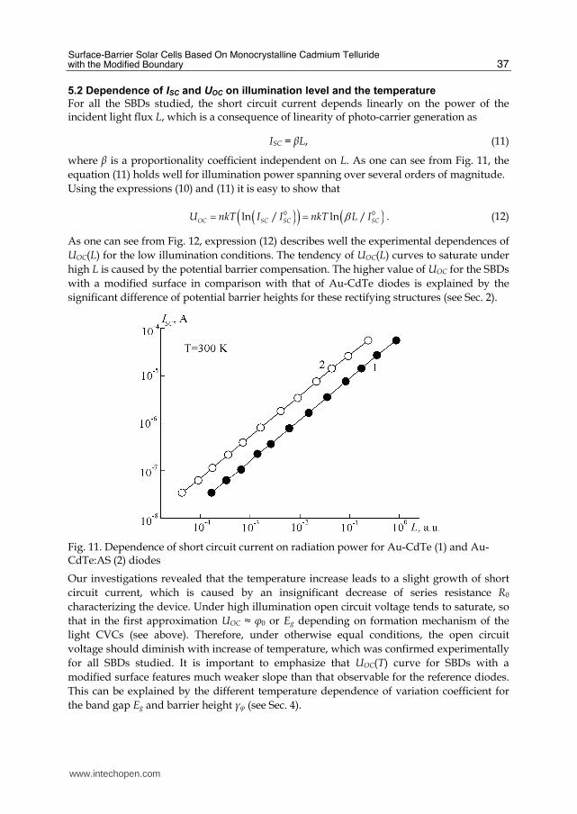
Surface-Barrier Solar Cells Based On Monocrystalline Cadmium Telluride with the Modified Boundary
37
52 Dependence of ISC and UOC on illumination level and the temperature
For all the SBDs studied the short circuit current depends linearly on the power of the incident light flux L which is a consequence of linearity of photo-carrier generation as
ISC = L (11)
where is a proportionality coefficient independent on L As one can see from Fig 11 the
equation (11) holds well for illumination power spanning over several orders of magnitude
Using the expressions (10) and (11) it is easy to show that
( )( ) ( )β= =0 0ln ln OC SC SC SCU nkT I I nkT L I (12)
As one can see from Fig 12 expression (12) describes well the experimental dependences of
UOC(L) for the low illumination conditions The tendency of UOC(L) curves to saturate under
high L is caused by the potential barrier compensation The higher value of UOC for the SBDs
with a modified surface in comparison with that of Au-CdTe diodes is explained by the
significant difference of potential barrier heights for these rectifying structures (see Sec 2)
Fig 11 Dependence of short circuit current on radiation power for Au-CdTe (1) and Au-CdTeAS (2) diodes
Our investigations revealed that the temperature increase leads to a slight growth of short
circuit current which is caused by an insignificant decrease of series resistance R0
characterizing the device Under high illumination open circuit voltage tends to saturate so
that in the first approximation UOC asymp φ0 or Eg depending on formation mechanism of the
light CVCs (see above) Therefore under otherwise equal conditions the open circuit
voltage should diminish with increase of temperature which was confirmed experimentally
for all SBDs studied It is important to emphasize that UOC(T) curve for SBDs with a
modified surface features much weaker slope than that observable for the reference diodes
This can be explained by the different temperature dependence of variation coefficient for
the band gap Eg and barrier height φ (see Sec 4)
wwwintechopencom
Solar Energy
38
Fig 12 Dependence of open circuit voltage on the illumination level for Au-CdTe (1) and Au-CdTeAS (2) diodes
53 Spectral characteristics
The previous investigations of optical electrical and photoelectrical properties of the SBDs predict several peculiar and promising characteristics of these structures In the first place the low energy limit ħωmin of the photosensitivity spectrum Sω is determined with high-energy edge of the transmission spectrum According to the data presented in Fig 5 the low-energy edge of Sω curves for Au-CdTe and Au-CdTeAS diodes will be about 15 eV while for Au-CdTeO2 contacts it is somewhat lower reaching 13 eV (Fig 13)
Fig 13 Photosensitivity spectra for the SBD based on the substrates of CdTe (1) CdTeAS (2) and CdTeO2 (3) at 300 K
High-energy photosensitivity as it was discussed above is defined by the surface
recombination rate which in turn depends on concentration of the defects NS at the junction
wwwintechopencom
Surface-Barrier Solar Cells Based On Monocrystalline Cadmium Telluride with the Modified Boundary
39
boundary Thus high short-wave sensitivity should be expected in SBDs based on the
substrates with a maximum efficiency of edge luminescence band This conclusion is
confirmed by the data presented in Fig 13 featuring wider photo-sensitivity peaks for Au-
CdTeO2 diodes which are based on the substrates with the most intensive A-band (see
Section 3) reaching 10 for 300 K At the same time for case of CdTeAS and CdTe
substrates the corresponding A-band values would be 1-2 and 001 respectively
strongly influencing the behavior of Sω spectra for photon energies ħω gt Eg (Fig 13)
Investigation of the temperature dependence of the SBD spectra reveals that higher values
of Т mainly affect their low-energy ldquotailrdquo The edge of Sω under the temperature varying in
the ranges 300-450 K almost replicates the dependence Eg(T) In the contrast to this the
temperature dependence of the surface defects (ie their concentration energy distribution
and scattering cross-sections) is negligibly weak as one may conclude from the
photosensitivity spectra for ħω gt Eg
Type of the surface barrier diode
Au-CdTe Au-CdTeAS Au-CdTeO2
φ0 eV 07 12 135
R0 Ω 30 30 32
UOC V 04 06 07
ISC mAcm2 10 15 22 Par
amet
ers
Efficiency 5 9 13
Table 1 Main parameters of the solar cells
54 Main parameters of surface barrier solar cells
The diodes with the effective photosensitive area of 210-2 cm2 were illuminated from the side of a semi-transparent golden contact by light equivalent to AM2 solar illumination conditions All the measurements were performed at 300 K and the best results obtained were summarized in Table 1 The values characterize photovoltaic devices in ldquoas-obtainedrdquo form without anti-reflection
coatings or any special optimization of solar cell design Due to this the values of fill factor
ff are under 07 because of considerable series resistance (see Table 1) The reduction of the
latter would allow increase of both ISC and ff improving the efficiency of the SCs
6 Conclusions
The authors developed a special technological approach consisting in a special surface
treatment of monocrystalline plates of cadmium telluride before deposition of the barrier
contact which significantly improves the electrical and photoelectric properties of the
surface-barrier devices of metal-semiconductor junction type created on their base The
wwwintechopencom
Solar Energy
40
annealing of n-CdTe substrates (ρ ~ 10-20 Ω cm) in the air or aquatic suspense of alkaline
metals increases the potential barrier height φ0 up to 12-14 eV in comparison with φ0 asymp 07
eV for non-annealed substrates The SBDs with modified surface features much better open
circuit voltage and short circuit current The efficiency of solar cells based on the diodes
studied under AM2 illumination was within the ranges 8-13 at the room temperature The
developed technology for surface-barrier solar cells is simple cheap and ecologically clean
In addition the proposed technological principles can be used for producing photovoltaic
devices based on thin films of cadmium telluride
7 Acknowledgements
This research was supported in part by the Ministry for Education and Science (Ukraine)
through the financing provided for the scientific projects carried out at the Department of
Optoelectronics Department of Energy Engineering and Electronics as well as at the
Science and Education Center ldquoSemiconductor Material Science and Energy-Efficient
Technologyrdquo at the Chernivtsi National University Research Project SU447-2009 for the
years 2009-2010 We also acknowledge the financial support of CONACYT (Meacutexico) for the
research performed in CINVESTAV-Quereacutetaro Research Project CB-2005-01-48792 for the
years 2007-2010
8 References
Alferov ZhI (1998) The history and the future of semiconductor structures Fiz Tekhn
Poluprov Vol 32 No 1 3-19
Amanullah FM (2003) Effect of isochronal annealing on CdTe and the study of electrical
properties of AundashCdTe Schottky devices Canadian Journal of Physics Vol 81 No 3
617-624
Andreev VM Dolginov LM amp Tretrsquoyakov DN (1975) Liquid epitaxy in technology of
semiconductor devices Soviet radio Moscow
Batavin VV Kontsevoj YuA amp Fedorovich YuV (1985) Measurement of the parameters of
semiconductor materials and structures Radio i svyazrsquo Moscow
Britt J amp Ferekides C (1993) Thin film CdSCdTe solar cell with 158 efficiency Applied
Physics Letters Vol 62 2851-2852
Chopra KL amp Das SR (1983) Thin film solar cells Springer New York
Ciach R Demich MV Gorley PM Kuznicki Z Makhniy VP Malimon IV amp
Swiatek Z (1999) Photo and X-ray sensitive heterostructures based on cadmium
telluride J Cryst Growth Vol 197 No 3 675-679
Donnet D (2001) Cadmium telluride solar sells In Crean Electricity from Photovoltaic
Archer MD amp Hill R (Eds) 245-276 Imperial College Press
Fahrenbruch AL amp Bube RH (1983) Fundamentals of solar cells photovoltaic solar energy
conversion Academic Press New York
Gnatyuk VA Aoki T Hatanaka Y amp Vlasenko OI (2005) Metalndashsemiconductor
interfaces in CdTe crystals and modification of their properties by laser pulses
Applied Surface Science Vol 244 528-532
wwwintechopencom
Surface-Barrier Solar Cells Based On Monocrystalline Cadmium Telluride with the Modified Boundary
41
Higa A Owan I Toyama H Yamazato M Ohno R amp Toguchi M (2007) Properties of
Al Schottky Contacts on CdTe(111)Cd Surface Treated by He and H2 Plasmas
Japanese Journal of Applied Physics Vol 46 2869-2872
Kesamanly FP amp Nasledov DN (Eds) (1973) Gallium arsenide production properties and
applications Nauka Moscow
Kim K Cho S Suh J Won J Hong J amp Kim S (2009) Schottky-type polycrystalline
CdZnTe X-ray detectors Current Applied Physics Vol 9 No 2 306-310
Koltun MM (1985) Optics and metrology of the solar cells Nauka Moscow
Koltun MM (1987) Solar cells Nauka Moscow
Korbutyak DV Melrsquonychuk SV Korbut YeV amp Borysyuk MM (2000) Cadmium
telluride impurity defect states and detector properties Ivan Fedoriv Kyiv
Madelung O (2004) Semiconductors Data Handbook Springer
Makhniy VP amp Skrypnyk MV (2008) Patent for the useful model UA 31891 published
25042008
Makhniy VP (1992) Physical processes in the diode structures based on wide-band A2B6
semiconductors Dissertation of the Doctor in Physics and Mathematics Chernivtsi
Makhniy VP Demych MV amp Slyotov MM (2003) Declaration patent UA 5010А
published 22042003
Makhniy VP Skrypnyk MV amp Demych MV (2009a) Patent for a useful model UA
40056 published 23052009
Makhniy VP Slyotov MM amp Skrypnyk NV (2009b) Peculiar optical properties of
modified surface of monocrystalline cadmium telluride Ukr J Phys Opt Vol 10
No 1 54-60
Makhniy VP Slyotov MM Stets EV Tkachenko IV Gorley VV amp Horley PP
(2004) Application of modulation spectroscopy for determination of recombination
center parameters Thin Solid Films Vol 450 222-225
Mason W Almeida LA Kaleczyc AW amp Dinan JH (2004) Electrical characterization of
CdCdTe Schottky barrier diodes Applied Physics Letters Vol 85 No 10 1730-1732
Milnes A amp Feucht D (1972) Heterojucntions and metal semiconductor junctions Academic
Press New York
Mizetskaya IB Oleynik GS Budennaya LD Tomashek VN amp Olejnik ND (1986) Physico-chemical bases for the synthesis of monocrystals of semiconductor solid solutions
AIIBVI Naukova dumka Kiev
Pool Ch Jr amp Owens F (2006) Nanotechnologies Tekhnosfera Moscow
Rhoderick EH (1982) Metal-semiconductor contacts Clarendon Press Oxford
Ryzhikov VD (1989) Scintillating crystals of the semiconductor compounds A2B6 Obtaining
properties applications NIITEKhIM Moscow
Sharma BL amp Purohit RK (1979) Semiconductor heterojunctions Soviet radio Moscow
Simashkevich AV (1980) Heterojunctions based on semiconductor AIIBVI compounds Sthtiintsa
Kishinev
Sites J amp Pan J (2007) Strategies to increase CdTe solar-cell voltage Thin Solid Films Vol
515 No 15 6099-6102
Strikha VI amp Kilrsquochitskaya SS (1992) Solar cells based on the contact metal-semiconductor
Energoatomizdat St Petersburg
wwwintechopencom
Solar Energy
42
Sze SM amp Kwok KNg (2007) Physics of semiconductor devices J Willey amp Sons New Jersey
Valiev KA Pashintsev YuI amp Petrov GV (1981) Using contacts metal-semiconductor in
electronics Soviet radio Moscow
Vorobiev YuV Dobrovolrsquoskiy VN amp Strikha VI (1988) Methods in semiconductor studies
Vyshcha shkola Kiev
Zayachuk DM (2006) Low-scale structures and super-lattices Lviv Polytechnic Lviv
wwwintechopencom
Solar EnergyEdited by Radu D Rugescu
ISBN 978-953-307-052-0Hard cover 432 pagesPublisher InTechPublished online 01 February 2010Published in print edition February 2010
InTech EuropeUniversity Campus STeP Ri Slavka Krautzeka 83A 51000 Rijeka Croatia Phone +385 (51) 770 447 Fax +385 (51) 686 166wwwintechopencom
InTech ChinaUnit 405 Office Block Hotel Equatorial Shanghai No65 Yan An Road (West) Shanghai 200040 China
Phone +86-21-62489820 Fax +86-21-62489821
The present ldquoSolar Energyrdquo science book hopefully opens a series of other first-hand texts in new technologieswith practical impact and subsequent interest They might include the ecological combustion of fossil fuelsspace technology in the benefit of local and remote communities new trends in the development of secureInternet Communications on an interplanetary scale new breakthroughs in the propulsion technology andothers The editors will be pleased to see that the present book is open to debate and they will wait for thereadersrsquo reaction with great interest Critics and proposals will be equally welcomed
How to referenceIn order to correctly reference this scholarly work feel free to copy and paste the following
PМ Gorley VP Makhniy PP Horley YuV Vorobiev and J Gonzaacutelez-Hernaacutendez (2010) Surface-BarrierSolar Cells Based On Monocrystalline Cadmium Telluride with the Modified Boundary Solar Energy Radu DRugescu (Ed) ISBN 978-953-307-052-0 InTech Available from httpwwwintechopencombookssolar-energysurface-barrier-solar-cells-based-on-monocrystalline-cadmium-telluride-with-the-modified-boundary
copy 2010 The Author(s) Licensee IntechOpen This chapter is distributedunder the terms of the Creative Commons Attribution-NonCommercial-ShareAlike-30 License which permits use distribution and reproduction fornon-commercial purposes provided the original is properly cited andderivative works building on this content are distributed under the samelicense

Solar Energy
38
Fig 12 Dependence of open circuit voltage on the illumination level for Au-CdTe (1) and Au-CdTeAS (2) diodes
53 Spectral characteristics
The previous investigations of optical electrical and photoelectrical properties of the SBDs predict several peculiar and promising characteristics of these structures In the first place the low energy limit ħωmin of the photosensitivity spectrum Sω is determined with high-energy edge of the transmission spectrum According to the data presented in Fig 5 the low-energy edge of Sω curves for Au-CdTe and Au-CdTeAS diodes will be about 15 eV while for Au-CdTeO2 contacts it is somewhat lower reaching 13 eV (Fig 13)
Fig 13 Photosensitivity spectra for the SBD based on the substrates of CdTe (1) CdTeAS (2) and CdTeO2 (3) at 300 K
High-energy photosensitivity as it was discussed above is defined by the surface
recombination rate which in turn depends on concentration of the defects NS at the junction
wwwintechopencom
Surface-Barrier Solar Cells Based On Monocrystalline Cadmium Telluride with the Modified Boundary
39
boundary Thus high short-wave sensitivity should be expected in SBDs based on the
substrates with a maximum efficiency of edge luminescence band This conclusion is
confirmed by the data presented in Fig 13 featuring wider photo-sensitivity peaks for Au-
CdTeO2 diodes which are based on the substrates with the most intensive A-band (see
Section 3) reaching 10 for 300 K At the same time for case of CdTeAS and CdTe
substrates the corresponding A-band values would be 1-2 and 001 respectively
strongly influencing the behavior of Sω spectra for photon energies ħω gt Eg (Fig 13)
Investigation of the temperature dependence of the SBD spectra reveals that higher values
of Т mainly affect their low-energy ldquotailrdquo The edge of Sω under the temperature varying in
the ranges 300-450 K almost replicates the dependence Eg(T) In the contrast to this the
temperature dependence of the surface defects (ie their concentration energy distribution
and scattering cross-sections) is negligibly weak as one may conclude from the
photosensitivity spectra for ħω gt Eg
Type of the surface barrier diode
Au-CdTe Au-CdTeAS Au-CdTeO2
φ0 eV 07 12 135
R0 Ω 30 30 32
UOC V 04 06 07
ISC mAcm2 10 15 22 Par
amet
ers
Efficiency 5 9 13
Table 1 Main parameters of the solar cells
54 Main parameters of surface barrier solar cells
The diodes with the effective photosensitive area of 210-2 cm2 were illuminated from the side of a semi-transparent golden contact by light equivalent to AM2 solar illumination conditions All the measurements were performed at 300 K and the best results obtained were summarized in Table 1 The values characterize photovoltaic devices in ldquoas-obtainedrdquo form without anti-reflection
coatings or any special optimization of solar cell design Due to this the values of fill factor
ff are under 07 because of considerable series resistance (see Table 1) The reduction of the
latter would allow increase of both ISC and ff improving the efficiency of the SCs
6 Conclusions
The authors developed a special technological approach consisting in a special surface
treatment of monocrystalline plates of cadmium telluride before deposition of the barrier
contact which significantly improves the electrical and photoelectric properties of the
surface-barrier devices of metal-semiconductor junction type created on their base The
wwwintechopencom
Solar Energy
40
annealing of n-CdTe substrates (ρ ~ 10-20 Ω cm) in the air or aquatic suspense of alkaline
metals increases the potential barrier height φ0 up to 12-14 eV in comparison with φ0 asymp 07
eV for non-annealed substrates The SBDs with modified surface features much better open
circuit voltage and short circuit current The efficiency of solar cells based on the diodes
studied under AM2 illumination was within the ranges 8-13 at the room temperature The
developed technology for surface-barrier solar cells is simple cheap and ecologically clean
In addition the proposed technological principles can be used for producing photovoltaic
devices based on thin films of cadmium telluride
7 Acknowledgements
This research was supported in part by the Ministry for Education and Science (Ukraine)
through the financing provided for the scientific projects carried out at the Department of
Optoelectronics Department of Energy Engineering and Electronics as well as at the
Science and Education Center ldquoSemiconductor Material Science and Energy-Efficient
Technologyrdquo at the Chernivtsi National University Research Project SU447-2009 for the
years 2009-2010 We also acknowledge the financial support of CONACYT (Meacutexico) for the
research performed in CINVESTAV-Quereacutetaro Research Project CB-2005-01-48792 for the
years 2007-2010
8 References
Alferov ZhI (1998) The history and the future of semiconductor structures Fiz Tekhn
Poluprov Vol 32 No 1 3-19
Amanullah FM (2003) Effect of isochronal annealing on CdTe and the study of electrical
properties of AundashCdTe Schottky devices Canadian Journal of Physics Vol 81 No 3
617-624
Andreev VM Dolginov LM amp Tretrsquoyakov DN (1975) Liquid epitaxy in technology of
semiconductor devices Soviet radio Moscow
Batavin VV Kontsevoj YuA amp Fedorovich YuV (1985) Measurement of the parameters of
semiconductor materials and structures Radio i svyazrsquo Moscow
Britt J amp Ferekides C (1993) Thin film CdSCdTe solar cell with 158 efficiency Applied
Physics Letters Vol 62 2851-2852
Chopra KL amp Das SR (1983) Thin film solar cells Springer New York
Ciach R Demich MV Gorley PM Kuznicki Z Makhniy VP Malimon IV amp
Swiatek Z (1999) Photo and X-ray sensitive heterostructures based on cadmium
telluride J Cryst Growth Vol 197 No 3 675-679
Donnet D (2001) Cadmium telluride solar sells In Crean Electricity from Photovoltaic
Archer MD amp Hill R (Eds) 245-276 Imperial College Press
Fahrenbruch AL amp Bube RH (1983) Fundamentals of solar cells photovoltaic solar energy
conversion Academic Press New York
Gnatyuk VA Aoki T Hatanaka Y amp Vlasenko OI (2005) Metalndashsemiconductor
interfaces in CdTe crystals and modification of their properties by laser pulses
Applied Surface Science Vol 244 528-532
wwwintechopencom
Surface-Barrier Solar Cells Based On Monocrystalline Cadmium Telluride with the Modified Boundary
41
Higa A Owan I Toyama H Yamazato M Ohno R amp Toguchi M (2007) Properties of
Al Schottky Contacts on CdTe(111)Cd Surface Treated by He and H2 Plasmas
Japanese Journal of Applied Physics Vol 46 2869-2872
Kesamanly FP amp Nasledov DN (Eds) (1973) Gallium arsenide production properties and
applications Nauka Moscow
Kim K Cho S Suh J Won J Hong J amp Kim S (2009) Schottky-type polycrystalline
CdZnTe X-ray detectors Current Applied Physics Vol 9 No 2 306-310
Koltun MM (1985) Optics and metrology of the solar cells Nauka Moscow
Koltun MM (1987) Solar cells Nauka Moscow
Korbutyak DV Melrsquonychuk SV Korbut YeV amp Borysyuk MM (2000) Cadmium
telluride impurity defect states and detector properties Ivan Fedoriv Kyiv
Madelung O (2004) Semiconductors Data Handbook Springer
Makhniy VP amp Skrypnyk MV (2008) Patent for the useful model UA 31891 published
25042008
Makhniy VP (1992) Physical processes in the diode structures based on wide-band A2B6
semiconductors Dissertation of the Doctor in Physics and Mathematics Chernivtsi
Makhniy VP Demych MV amp Slyotov MM (2003) Declaration patent UA 5010А
published 22042003
Makhniy VP Skrypnyk MV amp Demych MV (2009a) Patent for a useful model UA
40056 published 23052009
Makhniy VP Slyotov MM amp Skrypnyk NV (2009b) Peculiar optical properties of
modified surface of monocrystalline cadmium telluride Ukr J Phys Opt Vol 10
No 1 54-60
Makhniy VP Slyotov MM Stets EV Tkachenko IV Gorley VV amp Horley PP
(2004) Application of modulation spectroscopy for determination of recombination
center parameters Thin Solid Films Vol 450 222-225
Mason W Almeida LA Kaleczyc AW amp Dinan JH (2004) Electrical characterization of
CdCdTe Schottky barrier diodes Applied Physics Letters Vol 85 No 10 1730-1732
Milnes A amp Feucht D (1972) Heterojucntions and metal semiconductor junctions Academic
Press New York
Mizetskaya IB Oleynik GS Budennaya LD Tomashek VN amp Olejnik ND (1986) Physico-chemical bases for the synthesis of monocrystals of semiconductor solid solutions
AIIBVI Naukova dumka Kiev
Pool Ch Jr amp Owens F (2006) Nanotechnologies Tekhnosfera Moscow
Rhoderick EH (1982) Metal-semiconductor contacts Clarendon Press Oxford
Ryzhikov VD (1989) Scintillating crystals of the semiconductor compounds A2B6 Obtaining
properties applications NIITEKhIM Moscow
Sharma BL amp Purohit RK (1979) Semiconductor heterojunctions Soviet radio Moscow
Simashkevich AV (1980) Heterojunctions based on semiconductor AIIBVI compounds Sthtiintsa
Kishinev
Sites J amp Pan J (2007) Strategies to increase CdTe solar-cell voltage Thin Solid Films Vol
515 No 15 6099-6102
Strikha VI amp Kilrsquochitskaya SS (1992) Solar cells based on the contact metal-semiconductor
Energoatomizdat St Petersburg
wwwintechopencom
Solar Energy
42
Sze SM amp Kwok KNg (2007) Physics of semiconductor devices J Willey amp Sons New Jersey
Valiev KA Pashintsev YuI amp Petrov GV (1981) Using contacts metal-semiconductor in
electronics Soviet radio Moscow
Vorobiev YuV Dobrovolrsquoskiy VN amp Strikha VI (1988) Methods in semiconductor studies
Vyshcha shkola Kiev
Zayachuk DM (2006) Low-scale structures and super-lattices Lviv Polytechnic Lviv
wwwintechopencom
Solar EnergyEdited by Radu D Rugescu
ISBN 978-953-307-052-0Hard cover 432 pagesPublisher InTechPublished online 01 February 2010Published in print edition February 2010
InTech EuropeUniversity Campus STeP Ri Slavka Krautzeka 83A 51000 Rijeka Croatia Phone +385 (51) 770 447 Fax +385 (51) 686 166wwwintechopencom
InTech ChinaUnit 405 Office Block Hotel Equatorial Shanghai No65 Yan An Road (West) Shanghai 200040 China
Phone +86-21-62489820 Fax +86-21-62489821
The present ldquoSolar Energyrdquo science book hopefully opens a series of other first-hand texts in new technologieswith practical impact and subsequent interest They might include the ecological combustion of fossil fuelsspace technology in the benefit of local and remote communities new trends in the development of secureInternet Communications on an interplanetary scale new breakthroughs in the propulsion technology andothers The editors will be pleased to see that the present book is open to debate and they will wait for thereadersrsquo reaction with great interest Critics and proposals will be equally welcomed
How to referenceIn order to correctly reference this scholarly work feel free to copy and paste the following
PМ Gorley VP Makhniy PP Horley YuV Vorobiev and J Gonzaacutelez-Hernaacutendez (2010) Surface-BarrierSolar Cells Based On Monocrystalline Cadmium Telluride with the Modified Boundary Solar Energy Radu DRugescu (Ed) ISBN 978-953-307-052-0 InTech Available from httpwwwintechopencombookssolar-energysurface-barrier-solar-cells-based-on-monocrystalline-cadmium-telluride-with-the-modified-boundary
copy 2010 The Author(s) Licensee IntechOpen This chapter is distributedunder the terms of the Creative Commons Attribution-NonCommercial-ShareAlike-30 License which permits use distribution and reproduction fornon-commercial purposes provided the original is properly cited andderivative works building on this content are distributed under the samelicense

Surface-Barrier Solar Cells Based On Monocrystalline Cadmium Telluride with the Modified Boundary
39
boundary Thus high short-wave sensitivity should be expected in SBDs based on the
substrates with a maximum efficiency of edge luminescence band This conclusion is
confirmed by the data presented in Fig 13 featuring wider photo-sensitivity peaks for Au-
CdTeO2 diodes which are based on the substrates with the most intensive A-band (see
Section 3) reaching 10 for 300 K At the same time for case of CdTeAS and CdTe
substrates the corresponding A-band values would be 1-2 and 001 respectively
strongly influencing the behavior of Sω spectra for photon energies ħω gt Eg (Fig 13)
Investigation of the temperature dependence of the SBD spectra reveals that higher values
of Т mainly affect their low-energy ldquotailrdquo The edge of Sω under the temperature varying in
the ranges 300-450 K almost replicates the dependence Eg(T) In the contrast to this the
temperature dependence of the surface defects (ie their concentration energy distribution
and scattering cross-sections) is negligibly weak as one may conclude from the
photosensitivity spectra for ħω gt Eg
Type of the surface barrier diode
Au-CdTe Au-CdTeAS Au-CdTeO2
φ0 eV 07 12 135
R0 Ω 30 30 32
UOC V 04 06 07
ISC mAcm2 10 15 22 Par
amet
ers
Efficiency 5 9 13
Table 1 Main parameters of the solar cells
54 Main parameters of surface barrier solar cells
The diodes with the effective photosensitive area of 210-2 cm2 were illuminated from the side of a semi-transparent golden contact by light equivalent to AM2 solar illumination conditions All the measurements were performed at 300 K and the best results obtained were summarized in Table 1 The values characterize photovoltaic devices in ldquoas-obtainedrdquo form without anti-reflection
coatings or any special optimization of solar cell design Due to this the values of fill factor
ff are under 07 because of considerable series resistance (see Table 1) The reduction of the
latter would allow increase of both ISC and ff improving the efficiency of the SCs
6 Conclusions
The authors developed a special technological approach consisting in a special surface
treatment of monocrystalline plates of cadmium telluride before deposition of the barrier
contact which significantly improves the electrical and photoelectric properties of the
surface-barrier devices of metal-semiconductor junction type created on their base The
wwwintechopencom
Solar Energy
40
annealing of n-CdTe substrates (ρ ~ 10-20 Ω cm) in the air or aquatic suspense of alkaline
metals increases the potential barrier height φ0 up to 12-14 eV in comparison with φ0 asymp 07
eV for non-annealed substrates The SBDs with modified surface features much better open
circuit voltage and short circuit current The efficiency of solar cells based on the diodes
studied under AM2 illumination was within the ranges 8-13 at the room temperature The
developed technology for surface-barrier solar cells is simple cheap and ecologically clean
In addition the proposed technological principles can be used for producing photovoltaic
devices based on thin films of cadmium telluride
7 Acknowledgements
This research was supported in part by the Ministry for Education and Science (Ukraine)
through the financing provided for the scientific projects carried out at the Department of
Optoelectronics Department of Energy Engineering and Electronics as well as at the
Science and Education Center ldquoSemiconductor Material Science and Energy-Efficient
Technologyrdquo at the Chernivtsi National University Research Project SU447-2009 for the
years 2009-2010 We also acknowledge the financial support of CONACYT (Meacutexico) for the
research performed in CINVESTAV-Quereacutetaro Research Project CB-2005-01-48792 for the
years 2007-2010
8 References
Alferov ZhI (1998) The history and the future of semiconductor structures Fiz Tekhn
Poluprov Vol 32 No 1 3-19
Amanullah FM (2003) Effect of isochronal annealing on CdTe and the study of electrical
properties of AundashCdTe Schottky devices Canadian Journal of Physics Vol 81 No 3
617-624
Andreev VM Dolginov LM amp Tretrsquoyakov DN (1975) Liquid epitaxy in technology of
semiconductor devices Soviet radio Moscow
Batavin VV Kontsevoj YuA amp Fedorovich YuV (1985) Measurement of the parameters of
semiconductor materials and structures Radio i svyazrsquo Moscow
Britt J amp Ferekides C (1993) Thin film CdSCdTe solar cell with 158 efficiency Applied
Physics Letters Vol 62 2851-2852
Chopra KL amp Das SR (1983) Thin film solar cells Springer New York
Ciach R Demich MV Gorley PM Kuznicki Z Makhniy VP Malimon IV amp
Swiatek Z (1999) Photo and X-ray sensitive heterostructures based on cadmium
telluride J Cryst Growth Vol 197 No 3 675-679
Donnet D (2001) Cadmium telluride solar sells In Crean Electricity from Photovoltaic
Archer MD amp Hill R (Eds) 245-276 Imperial College Press
Fahrenbruch AL amp Bube RH (1983) Fundamentals of solar cells photovoltaic solar energy
conversion Academic Press New York
Gnatyuk VA Aoki T Hatanaka Y amp Vlasenko OI (2005) Metalndashsemiconductor
interfaces in CdTe crystals and modification of their properties by laser pulses
Applied Surface Science Vol 244 528-532
wwwintechopencom
Surface-Barrier Solar Cells Based On Monocrystalline Cadmium Telluride with the Modified Boundary
41
Higa A Owan I Toyama H Yamazato M Ohno R amp Toguchi M (2007) Properties of
Al Schottky Contacts on CdTe(111)Cd Surface Treated by He and H2 Plasmas
Japanese Journal of Applied Physics Vol 46 2869-2872
Kesamanly FP amp Nasledov DN (Eds) (1973) Gallium arsenide production properties and
applications Nauka Moscow
Kim K Cho S Suh J Won J Hong J amp Kim S (2009) Schottky-type polycrystalline
CdZnTe X-ray detectors Current Applied Physics Vol 9 No 2 306-310
Koltun MM (1985) Optics and metrology of the solar cells Nauka Moscow
Koltun MM (1987) Solar cells Nauka Moscow
Korbutyak DV Melrsquonychuk SV Korbut YeV amp Borysyuk MM (2000) Cadmium
telluride impurity defect states and detector properties Ivan Fedoriv Kyiv
Madelung O (2004) Semiconductors Data Handbook Springer
Makhniy VP amp Skrypnyk MV (2008) Patent for the useful model UA 31891 published
25042008
Makhniy VP (1992) Physical processes in the diode structures based on wide-band A2B6
semiconductors Dissertation of the Doctor in Physics and Mathematics Chernivtsi
Makhniy VP Demych MV amp Slyotov MM (2003) Declaration patent UA 5010А
published 22042003
Makhniy VP Skrypnyk MV amp Demych MV (2009a) Patent for a useful model UA
40056 published 23052009
Makhniy VP Slyotov MM amp Skrypnyk NV (2009b) Peculiar optical properties of
modified surface of monocrystalline cadmium telluride Ukr J Phys Opt Vol 10
No 1 54-60
Makhniy VP Slyotov MM Stets EV Tkachenko IV Gorley VV amp Horley PP
(2004) Application of modulation spectroscopy for determination of recombination
center parameters Thin Solid Films Vol 450 222-225
Mason W Almeida LA Kaleczyc AW amp Dinan JH (2004) Electrical characterization of
CdCdTe Schottky barrier diodes Applied Physics Letters Vol 85 No 10 1730-1732
Milnes A amp Feucht D (1972) Heterojucntions and metal semiconductor junctions Academic
Press New York
Mizetskaya IB Oleynik GS Budennaya LD Tomashek VN amp Olejnik ND (1986) Physico-chemical bases for the synthesis of monocrystals of semiconductor solid solutions
AIIBVI Naukova dumka Kiev
Pool Ch Jr amp Owens F (2006) Nanotechnologies Tekhnosfera Moscow
Rhoderick EH (1982) Metal-semiconductor contacts Clarendon Press Oxford
Ryzhikov VD (1989) Scintillating crystals of the semiconductor compounds A2B6 Obtaining
properties applications NIITEKhIM Moscow
Sharma BL amp Purohit RK (1979) Semiconductor heterojunctions Soviet radio Moscow
Simashkevich AV (1980) Heterojunctions based on semiconductor AIIBVI compounds Sthtiintsa
Kishinev
Sites J amp Pan J (2007) Strategies to increase CdTe solar-cell voltage Thin Solid Films Vol
515 No 15 6099-6102
Strikha VI amp Kilrsquochitskaya SS (1992) Solar cells based on the contact metal-semiconductor
Energoatomizdat St Petersburg
wwwintechopencom
Solar Energy
42
Sze SM amp Kwok KNg (2007) Physics of semiconductor devices J Willey amp Sons New Jersey
Valiev KA Pashintsev YuI amp Petrov GV (1981) Using contacts metal-semiconductor in
electronics Soviet radio Moscow
Vorobiev YuV Dobrovolrsquoskiy VN amp Strikha VI (1988) Methods in semiconductor studies
Vyshcha shkola Kiev
Zayachuk DM (2006) Low-scale structures and super-lattices Lviv Polytechnic Lviv
wwwintechopencom
Solar EnergyEdited by Radu D Rugescu
ISBN 978-953-307-052-0Hard cover 432 pagesPublisher InTechPublished online 01 February 2010Published in print edition February 2010
InTech EuropeUniversity Campus STeP Ri Slavka Krautzeka 83A 51000 Rijeka Croatia Phone +385 (51) 770 447 Fax +385 (51) 686 166wwwintechopencom
InTech ChinaUnit 405 Office Block Hotel Equatorial Shanghai No65 Yan An Road (West) Shanghai 200040 China
Phone +86-21-62489820 Fax +86-21-62489821
The present ldquoSolar Energyrdquo science book hopefully opens a series of other first-hand texts in new technologieswith practical impact and subsequent interest They might include the ecological combustion of fossil fuelsspace technology in the benefit of local and remote communities new trends in the development of secureInternet Communications on an interplanetary scale new breakthroughs in the propulsion technology andothers The editors will be pleased to see that the present book is open to debate and they will wait for thereadersrsquo reaction with great interest Critics and proposals will be equally welcomed
How to referenceIn order to correctly reference this scholarly work feel free to copy and paste the following
PМ Gorley VP Makhniy PP Horley YuV Vorobiev and J Gonzaacutelez-Hernaacutendez (2010) Surface-BarrierSolar Cells Based On Monocrystalline Cadmium Telluride with the Modified Boundary Solar Energy Radu DRugescu (Ed) ISBN 978-953-307-052-0 InTech Available from httpwwwintechopencombookssolar-energysurface-barrier-solar-cells-based-on-monocrystalline-cadmium-telluride-with-the-modified-boundary
copy 2010 The Author(s) Licensee IntechOpen This chapter is distributedunder the terms of the Creative Commons Attribution-NonCommercial-ShareAlike-30 License which permits use distribution and reproduction fornon-commercial purposes provided the original is properly cited andderivative works building on this content are distributed under the samelicense

Solar Energy
40
annealing of n-CdTe substrates (ρ ~ 10-20 Ω cm) in the air or aquatic suspense of alkaline
metals increases the potential barrier height φ0 up to 12-14 eV in comparison with φ0 asymp 07
eV for non-annealed substrates The SBDs with modified surface features much better open
circuit voltage and short circuit current The efficiency of solar cells based on the diodes
studied under AM2 illumination was within the ranges 8-13 at the room temperature The
developed technology for surface-barrier solar cells is simple cheap and ecologically clean
In addition the proposed technological principles can be used for producing photovoltaic
devices based on thin films of cadmium telluride
7 Acknowledgements
This research was supported in part by the Ministry for Education and Science (Ukraine)
through the financing provided for the scientific projects carried out at the Department of
Optoelectronics Department of Energy Engineering and Electronics as well as at the
Science and Education Center ldquoSemiconductor Material Science and Energy-Efficient
Technologyrdquo at the Chernivtsi National University Research Project SU447-2009 for the
years 2009-2010 We also acknowledge the financial support of CONACYT (Meacutexico) for the
research performed in CINVESTAV-Quereacutetaro Research Project CB-2005-01-48792 for the
years 2007-2010
8 References
Alferov ZhI (1998) The history and the future of semiconductor structures Fiz Tekhn
Poluprov Vol 32 No 1 3-19
Amanullah FM (2003) Effect of isochronal annealing on CdTe and the study of electrical
properties of AundashCdTe Schottky devices Canadian Journal of Physics Vol 81 No 3
617-624
Andreev VM Dolginov LM amp Tretrsquoyakov DN (1975) Liquid epitaxy in technology of
semiconductor devices Soviet radio Moscow
Batavin VV Kontsevoj YuA amp Fedorovich YuV (1985) Measurement of the parameters of
semiconductor materials and structures Radio i svyazrsquo Moscow
Britt J amp Ferekides C (1993) Thin film CdSCdTe solar cell with 158 efficiency Applied
Physics Letters Vol 62 2851-2852
Chopra KL amp Das SR (1983) Thin film solar cells Springer New York
Ciach R Demich MV Gorley PM Kuznicki Z Makhniy VP Malimon IV amp
Swiatek Z (1999) Photo and X-ray sensitive heterostructures based on cadmium
telluride J Cryst Growth Vol 197 No 3 675-679
Donnet D (2001) Cadmium telluride solar sells In Crean Electricity from Photovoltaic
Archer MD amp Hill R (Eds) 245-276 Imperial College Press
Fahrenbruch AL amp Bube RH (1983) Fundamentals of solar cells photovoltaic solar energy
conversion Academic Press New York
Gnatyuk VA Aoki T Hatanaka Y amp Vlasenko OI (2005) Metalndashsemiconductor
interfaces in CdTe crystals and modification of their properties by laser pulses
Applied Surface Science Vol 244 528-532
wwwintechopencom
Surface-Barrier Solar Cells Based On Monocrystalline Cadmium Telluride with the Modified Boundary
41
Higa A Owan I Toyama H Yamazato M Ohno R amp Toguchi M (2007) Properties of
Al Schottky Contacts on CdTe(111)Cd Surface Treated by He and H2 Plasmas
Japanese Journal of Applied Physics Vol 46 2869-2872
Kesamanly FP amp Nasledov DN (Eds) (1973) Gallium arsenide production properties and
applications Nauka Moscow
Kim K Cho S Suh J Won J Hong J amp Kim S (2009) Schottky-type polycrystalline
CdZnTe X-ray detectors Current Applied Physics Vol 9 No 2 306-310
Koltun MM (1985) Optics and metrology of the solar cells Nauka Moscow
Koltun MM (1987) Solar cells Nauka Moscow
Korbutyak DV Melrsquonychuk SV Korbut YeV amp Borysyuk MM (2000) Cadmium
telluride impurity defect states and detector properties Ivan Fedoriv Kyiv
Madelung O (2004) Semiconductors Data Handbook Springer
Makhniy VP amp Skrypnyk MV (2008) Patent for the useful model UA 31891 published
25042008
Makhniy VP (1992) Physical processes in the diode structures based on wide-band A2B6
semiconductors Dissertation of the Doctor in Physics and Mathematics Chernivtsi
Makhniy VP Demych MV amp Slyotov MM (2003) Declaration patent UA 5010А
published 22042003
Makhniy VP Skrypnyk MV amp Demych MV (2009a) Patent for a useful model UA
40056 published 23052009
Makhniy VP Slyotov MM amp Skrypnyk NV (2009b) Peculiar optical properties of
modified surface of monocrystalline cadmium telluride Ukr J Phys Opt Vol 10
No 1 54-60
Makhniy VP Slyotov MM Stets EV Tkachenko IV Gorley VV amp Horley PP
(2004) Application of modulation spectroscopy for determination of recombination
center parameters Thin Solid Films Vol 450 222-225
Mason W Almeida LA Kaleczyc AW amp Dinan JH (2004) Electrical characterization of
CdCdTe Schottky barrier diodes Applied Physics Letters Vol 85 No 10 1730-1732
Milnes A amp Feucht D (1972) Heterojucntions and metal semiconductor junctions Academic
Press New York
Mizetskaya IB Oleynik GS Budennaya LD Tomashek VN amp Olejnik ND (1986) Physico-chemical bases for the synthesis of monocrystals of semiconductor solid solutions
AIIBVI Naukova dumka Kiev
Pool Ch Jr amp Owens F (2006) Nanotechnologies Tekhnosfera Moscow
Rhoderick EH (1982) Metal-semiconductor contacts Clarendon Press Oxford
Ryzhikov VD (1989) Scintillating crystals of the semiconductor compounds A2B6 Obtaining
properties applications NIITEKhIM Moscow
Sharma BL amp Purohit RK (1979) Semiconductor heterojunctions Soviet radio Moscow
Simashkevich AV (1980) Heterojunctions based on semiconductor AIIBVI compounds Sthtiintsa
Kishinev
Sites J amp Pan J (2007) Strategies to increase CdTe solar-cell voltage Thin Solid Films Vol
515 No 15 6099-6102
Strikha VI amp Kilrsquochitskaya SS (1992) Solar cells based on the contact metal-semiconductor
Energoatomizdat St Petersburg
wwwintechopencom
Solar Energy
42
Sze SM amp Kwok KNg (2007) Physics of semiconductor devices J Willey amp Sons New Jersey
Valiev KA Pashintsev YuI amp Petrov GV (1981) Using contacts metal-semiconductor in
electronics Soviet radio Moscow
Vorobiev YuV Dobrovolrsquoskiy VN amp Strikha VI (1988) Methods in semiconductor studies
Vyshcha shkola Kiev
Zayachuk DM (2006) Low-scale structures and super-lattices Lviv Polytechnic Lviv
wwwintechopencom
Solar EnergyEdited by Radu D Rugescu
ISBN 978-953-307-052-0Hard cover 432 pagesPublisher InTechPublished online 01 February 2010Published in print edition February 2010
InTech EuropeUniversity Campus STeP Ri Slavka Krautzeka 83A 51000 Rijeka Croatia Phone +385 (51) 770 447 Fax +385 (51) 686 166wwwintechopencom
InTech ChinaUnit 405 Office Block Hotel Equatorial Shanghai No65 Yan An Road (West) Shanghai 200040 China
Phone +86-21-62489820 Fax +86-21-62489821
The present ldquoSolar Energyrdquo science book hopefully opens a series of other first-hand texts in new technologieswith practical impact and subsequent interest They might include the ecological combustion of fossil fuelsspace technology in the benefit of local and remote communities new trends in the development of secureInternet Communications on an interplanetary scale new breakthroughs in the propulsion technology andothers The editors will be pleased to see that the present book is open to debate and they will wait for thereadersrsquo reaction with great interest Critics and proposals will be equally welcomed
How to referenceIn order to correctly reference this scholarly work feel free to copy and paste the following
PМ Gorley VP Makhniy PP Horley YuV Vorobiev and J Gonzaacutelez-Hernaacutendez (2010) Surface-BarrierSolar Cells Based On Monocrystalline Cadmium Telluride with the Modified Boundary Solar Energy Radu DRugescu (Ed) ISBN 978-953-307-052-0 InTech Available from httpwwwintechopencombookssolar-energysurface-barrier-solar-cells-based-on-monocrystalline-cadmium-telluride-with-the-modified-boundary
copy 2010 The Author(s) Licensee IntechOpen This chapter is distributedunder the terms of the Creative Commons Attribution-NonCommercial-ShareAlike-30 License which permits use distribution and reproduction fornon-commercial purposes provided the original is properly cited andderivative works building on this content are distributed under the samelicense

copy 2010 The Author(s) Licensee IntechOpen This chapter is distributedunder the terms of the Creative Commons Attribution-NonCommercial-ShareAlike-30 License which permits use distribution and reproduction fornon-commercial purposes provided the original is properly cited andderivative works building on this content are distributed under the samelicense