Embed Size (px)
Citation preview
1
Supporting Material
Probing Nanoscale Variations in Strain and Band Structure of MoS2 on Au Nanopyramids Using Tip-Enhanced Raman Spectroscopy
Zhongjian Zhang1, Alex C. De Palma1, Christopher J. Brennan1, Gabriel Cossio1, Rudresh Ghosh1, Sanjay K. Banerjee1, and Edward T. Yu1,* 1Microelectronics Research Center, University of Texas, Austin, Texas, 78758, USA
*Email: [email protected]
Table of Contents
Section 1. MoS2 Transfer and Characterization .............................................................................. 2
Section 2. Nanopyramid Fabrication ............................................................................................. 3
Section 3. Strain Calculations ......................................................................................................... 4
Section 4. Density Functional Theory Simulations ........................................................................ 5
Section 5. Raman and Photoluminescence Enhancement ............................................................... 8
Section 6. Additional Raman Data ................................................................................................ 10
References ..................................................................................................................................... 11
2
Section 1. MoS2 Transfer and Characterization
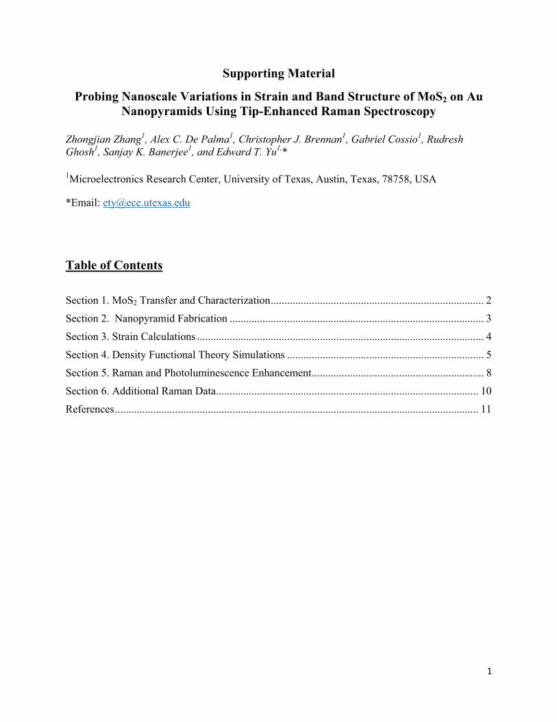
FIG. S1. Schematic drawings of process flow for polydimethylsiloxane (PDMS) stamp transfer process
MoS2 was transferred from the growth substrate on to both a flat Au substrate or the patterned Au nanopyramid substrate using a polydimethylsiloxane (PDMS) stamp and water transfer process. The as-grown MoS2 is under approximately 0.21% residual tensile strain, which is relaxed under the transfer process. The PDMS stamp is applied to a region of the growth substrate with atomically thin MoS2. To separate the MoS2 from the growth substrate, the substrate, MoS2 and stamped PDMS is placed in a water bath. The PDMS stamp with the MoS2 is then pressed on to either the flat or patterned Au substrates and heated with a hot plate to 50° C. Slowly peeling away the PDMS transfers the MoS2 to the substrate.
FIG. S2. MoS2 transferred onto a flat Au substrate with (a) optical and (b) atomic force microscopy (AFM) images of typical sample areas
Monolayer and bilayer regions initially distinguished in optical images by the differences in color. AFM images allow accurate determination of sample thickness, which allow controllable TERS and TEPL measurements.
3
Section 2. Nanopyramid Fabrication
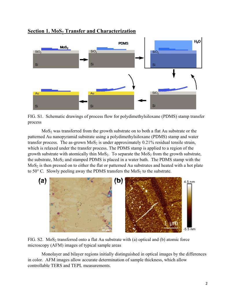
FIG. S3. (a) Schematic drawings of the fabrication work flow for creating the Au nanopyramid arrays. (b) Schematic drawing of self-assembled hexagonal nanosphere array.
Fig. S3(a) shows a fabrication work flow for the creation of Au nanopyramid structures on a Si substrate. First, we first deposit a single layer of 1 micron diameter nanospheres on the surface of an Si substrate where the nanospheres have self-assembled into hexagonal arrays leaving triangular shaped holes between the nanospheres. A schematic drawing of the self-assembled hexagonal array of nanospheres is shown in Fig. S3(b). The nanosphere array acts as a mask for subsequent deposition of a nm thick layer of dielectric, Al2O3, using electron beam deposition to create nanopyramid structures within the triangular shaped holes. The nanospheres are then lifted off through sonication in toluene leaving only the nanopyramid structures on the surface. Finally, a 5/65 nm thick Cr/Au bilayer is deposited using electron beam deposition on the substrate creating Au nanopyramids. The same previously mentioned PDMS stamp transfer process is then used to transfer CVD grown MoS2 onto the finished patterned substrate.

4
Section 3. Strain Calculations
To estimate the maximum strain using the spherical pure bending method1, where the structure is modeled as a surface wrapped around a sphere, the following equation is applied: ~ (1),
where t is the thickness of the MoS2 sample, R is the radius of curvature at the apex of the nanopyramid and is the residual strain, which is a fitting parameter. Taking the thickness to be 1.3 nm, the radius of curvature to be 40 nm and the residual strain to be 0, we estimate a maximum strain of 1.65%.
Approximating the MoS2 profile as a one-dimensional buckle delamination2, we can apply the following equation to estimate a maximum uniaxial strain: ~ (2),
where t is the thickness of the MoS2 sample, h is the height of the buckle, σ is Poisson’s ratio for MoS2 and λ is the width of the buckle. Taking the thickness to be 1.3 nm, the height to be 120 nm, Poisson’s ratio to be 0.125, and the width to be 400 nm, we estimate a maximum strain of 1.02%.
5
Section 4. Density Functional Theory Simulations
Band Structure Discussion
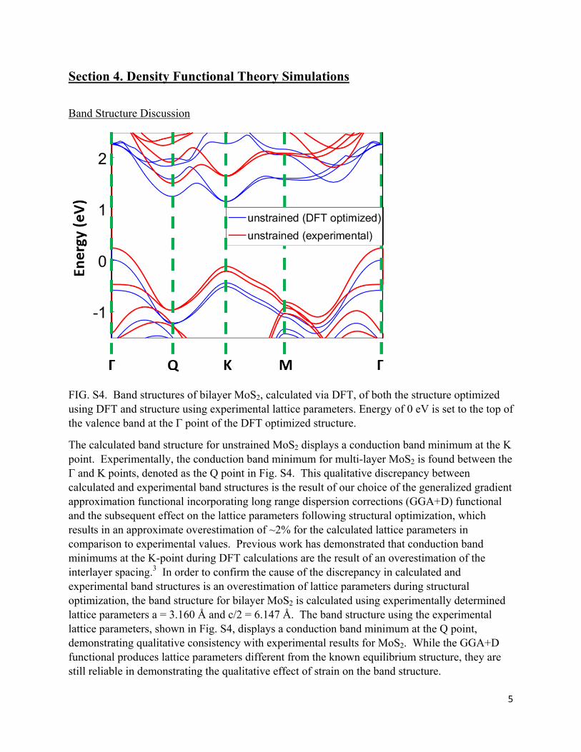
FIG. S4. Band structures of bilayer MoS2, calculated via DFT, of both the structure optimized using DFT and structure using experimental lattice parameters. Energy of 0 eV is set to the top of the valence band at the Γ point of the DFT optimized structure.
The calculated band structure for unstrained MoS2 displays a conduction band minimum at the K point. Experimentally, the conduction band minimum for multi-layer MoS2 is found between the Γ and K points, denoted as the Q point in Fig. S4. This qualitative discrepancy between calculated and experimental band structures is the result of our choice of the generalized gradient approximation functional incorporating long range dispersion corrections (GGA+D) functional and the subsequent effect on the lattice parameters following structural optimization, which results in an approximate overestimation of ~2% for the calculated lattice parameters in comparison to experimental values. Previous work has demonstrated that conduction band minimums at the K-point during DFT calculations are the result of an overestimation of the interlayer spacing.3 In order to confirm the cause of the discrepancy in calculated and experimental band structures is an overestimation of lattice parameters during structural optimization, the band structure for bilayer MoS2 is calculated using experimentally determined lattice parameters a = 3.160 Å and c/2 = 6.147 Å. The band structure using the experimental lattice parameters, shown in Fig. S4, displays a conduction band minimum at the Q point, demonstrating qualitative consistency with experimental results for MoS2. While the GGA+D functional produces lattice parameters different from the known equilibrium structure, they are still reliable in demonstrating the qualitative effect of strain on the band structure.
6
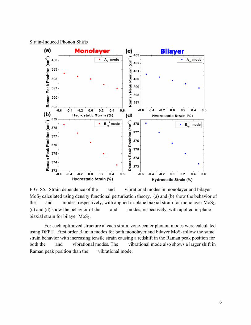
Strain-Induced Phonon Shifts
FIG. S5. Strain dependence of the and vibrational modes in monolayer and bilayer MoS2 calculated using density functional perturbation theory. (a) and (b) show the behavior of the and modes, respectively, with applied in-plane biaxial strain for monolayer MoS2. (c) and (d) show the behavior of the and modes, respectively, with applied in-plane biaxial strain for bilayer MoS2.
For each optimized structure at each strain, zone-center phonon modes were calculated using DFPT. First order Raman modes for both monolayer and bilayer MoS2 follow the same strain behavior with increasing tensile strain causing a redshift in the Raman peak position for both the and vibrational modes. The vibrational mode also shows a larger shift in Raman peak position than the vibrational mode.
7
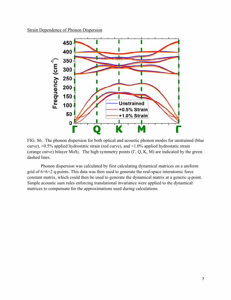
Strain Dependence of Phonon Dispersion
FIG. S6. The phonon dispersion for both optical and acoustic phonon modes for unstrained (blue curve), +0.5% applied hydrostatic strain (red curve), and +1.0% applied hydrostatic strain (orange curve) bilayer MoS2. The high symmetry points (Γ, Q, K, M) are indicated by the green dashed lines.
Phonon dispersion was calculated by first calculating dynamical matrices on a uniform grid of 6×6×2 q-points. This data was then used to generate the real-space interatomic force constant matrix, which could then be used to generate the dynamical matrix at a generic q-point. Simple acoustic sum rules enforcing translational invariance were applied to the dynamical matrices to compensate for the approximations used during calculations.
8
Section 5. Raman and Photoluminescence Enhancement
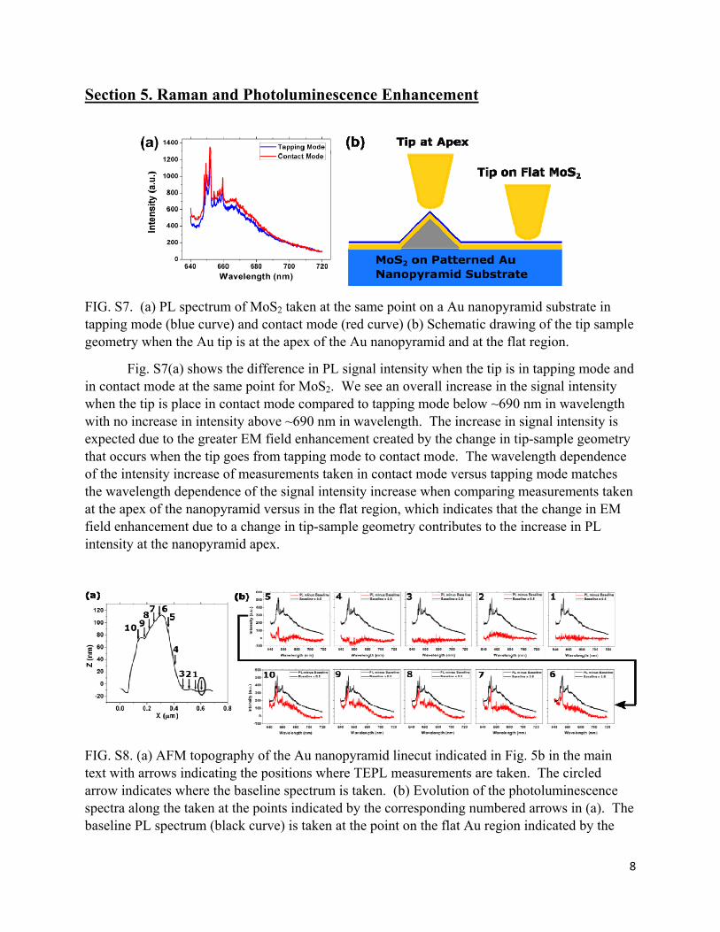
FIG. S7. (a) PL spectrum of MoS2 taken at the same point on a Au nanopyramid substrate in tapping mode (blue curve) and contact mode (red curve) (b) Schematic drawing of the tip sample geometry when the Au tip is at the apex of the Au nanopyramid and at the flat region.
Fig. S7(a) shows the difference in PL signal intensity when the tip is in tapping mode and in contact mode at the same point for MoS2. We see an overall increase in the signal intensity when the tip is place in contact mode compared to tapping mode below ~690 nm in wavelength with no increase in intensity above ~690 nm in wavelength. The increase in signal intensity is expected due to the greater EM field enhancement created by the change in tip-sample geometry that occurs when the tip goes from tapping mode to contact mode. The wavelength dependence of the intensity increase of measurements taken in contact mode versus tapping mode matches the wavelength dependence of the signal intensity increase when comparing measurements taken at the apex of the nanopyramid versus in the flat region, which indicates that the change in EM field enhancement due to a change in tip-sample geometry contributes to the increase in PL intensity at the nanopyramid apex.
FIG. S8. (a) AFM topography of the Au nanopyramid linecut indicated in Fig. 5b in the main text with arrows indicating the positions where TEPL measurements are taken. The circled arrow indicates where the baseline spectrum is taken. (b) Evolution of the photoluminescence spectra along the taken at the points indicated by the corresponding numbered arrows in (a). The baseline PL spectrum (black curve) is taken at the point on the flat Au region indicated by the

9
circled arrow in Fig 5(c). The PL spectrum at each point (red curve) has the baseline spectrum subtracted.
Fig. S8(b) shows the evolution of the Raman spectra taken at points indicated by the arrows with the corresponding arrows in Fig. S7(a). We observe increased PL intensity with additional luminescence shifted to longer wavelengths (~670 nm to ~690 nm) as tensile strain increases as the measurement points approach the apex of the pyramid, which is consistent with the strain induced lowering of the bandgap energy in bilayer MoS2.
10
Section 6. Additional Raman Data
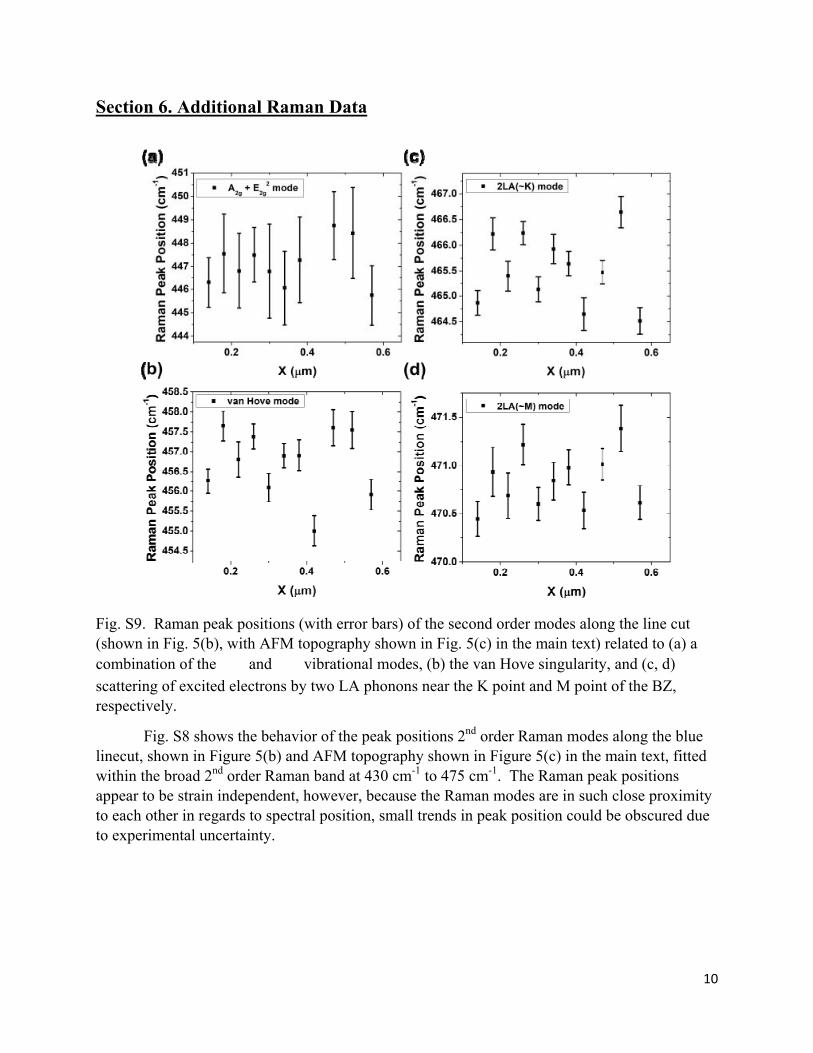
Fig. S9. Raman peak positions (with error bars) of the second order modes along the line cut (shown in Fig. 5(b), with AFM topography shown in Fig. 5(c) in the main text) related to (a) a combination of the and vibrational modes, (b) the van Hove singularity, and (c, d) scattering of excited electrons by two LA phonons near the K point and M point of the BZ, respectively.
Fig. S8 shows the behavior of the peak positions 2nd order Raman modes along the blue linecut, shown in Figure 5(b) and AFM topography shown in Figure 5(c) in the main text, fitted within the broad 2nd order Raman band at 430 cm-1 to 475 cm-1. The Raman peak positions appear to be strain independent, however, because the Raman modes are in such close proximity to each other in regards to spectral position, small trends in peak position could be obscured due to experimental uncertainty.
11
References 1 B.G. Shin, G.H. Han, S.J. Yun, H.M. Oh, J.J. Bae, Y.J. Song, C.Y. Park, and Y.H. Lee, Adv. Mater. 28, 9378 (2016). 2 A. Castellanos-Gomez, R. Roldán, E. Cappelluti, M. Buscema, F. Guinea, H.S.J. van der Zant, and G.A. Steele, Nano Lett. 13, 5361 (2013). 3 A. Ramasubramaniam, D. Naveh, and E. Towe, Phys. Rev. B 84, 205325 (2011).