Embed Size (px)
Citation preview
Supporting information to “Internal Photoemission (IPE) in Molecular Junctions: Parameters for Interfacial Barrier Determinations”
S1
Supporting Information For: “Internal Photoemission in Molecular
Junctions: Parameters for Interfacial Barrier Determinations”
Jerry A. Fereiro1, Mykola Kondratenko1,2, Adam Johan Bergren*2, Richard L. McCreery*1,2
1Department of Chemistry, University of Alberta, Edmonton, AB
2National Institute for Nanotechnology, National Research Council Canada
*Correspondence to: [email protected] (AJB), [email protected] (RLM);
Supporting information to “Internal Photoemission (IPE) in Molecular Junctions: Parameters for Interfacial Barrier Determinations”
S2
Introduction
This document contains additional supporting data, figures, discussions, and equations used to
support the main text. Specifically:
1. Schematic representation of the junction structure.
2. Molecular structures.
3. Experimental apparatus: Modulated source apparatus and DC laser source measurements.
4. Method for determining the absorption spectra of molecular layers.
5. Optical absorption spectra and determining the onset of optical absorption.
6. Excitation-intensity profiles for alkanes and related analysis for multiple molecules.
7. Optical absorption spectra of Fc and NDI molecule with their structures.
8. Yield vs. molecular thickness plot AB, NAB, NDI and Fc.
9. Fowler plots.

Supporting information to “Internal Photoemission (IPE) in Molecular Junctions: Parameters for Interfacial Barrier Determinations”
S3
1. Schematic representation of the junction structure:
Figure S1: Schematic representation of the junction structure.
Figure S1 shows the schematic of the junction structure used in this study. Details of junction
fabrication1 and the photocurrent measurement can be found in the supporting information of a
previously published paper2. Briefly, a narrow band (∆𝜆=13nm) of light from a xenon arc source
(Newport model 6256) passes through an optical chopper before incidence onto the top of a
molecular junction. A dual phase LIA is used to measure both the phase and the magnitude of the
photocurrent simultaneously.

Supporting information to “Internal Photoemission (IPE) in Molecular Junctions: Parameters for Interfacial Barrier Determinations”
S4
2. Molecular Structures:
Figure S2: The structures of all the molecules used in this study. (A) NDI; (B) Anthraquinone; (C) Azobenzene; (D) Ferrocene; (E) Bromophenyl; (F) Nitroazobenzene; (G) Alkane (C12H25N). In most cases, molecular layers were multilayers of several molecules, with thicknesses indicated in main text.
3. Experimental apparatus:
Figure S3-A: Apparatus with Xe arc continuum source, modulation by an optical chopper and
detection with a Lock-In -Amplifier (LIA).
NDI
A)
Anthraquinone
B)
Azobenzene
C)
Ferrocene
D)
Bromophenyl
E)
Alkane(C12)
G)
Nitro Azobenzene
F)
Sample
150 W Xe lampMonochromator
ChopperPhoton Energy : 1.5 eV - 6 eV
PPF
Cu
+
Dual Phase LIAIN
Chopper controller
Reference input
Focussing lens
Probes
Plane mirror
Collimating lens
Chopper
Lab ViewMagnitude Out
Phase Out
Supporting information to “Internal Photoemission (IPE) in Molecular Junctions: Parameters for Interfacial Barrier Determinations”
S5
Figure S3-A shows a diagram of the experiment using a 150 W Xenon arc lamp (Newport model
6256) as the source of illumination. After passing through a Newport model 74004 Cornerstone
130 1/8 m motorized monochromator (band pass = 13 nm), the selected wavelength was chopped
at frequency ω (typically 400 Hz). The chopped light was then directed through a series of lenses
and mirrors for focusing. The PPF contact was connected via a tungsten probe and shielded cable
to the AC-coupled current input of a dual phase lock-in amplifier (LIA, Stanford-830), and the
shield (ground) was connected to the Cu contact of the molecular junction. The output from the
LIA was recorded using a Labview data acquisition program. In all cases, the PPF was
considered the positive terminal, as shown in Figure S3A.
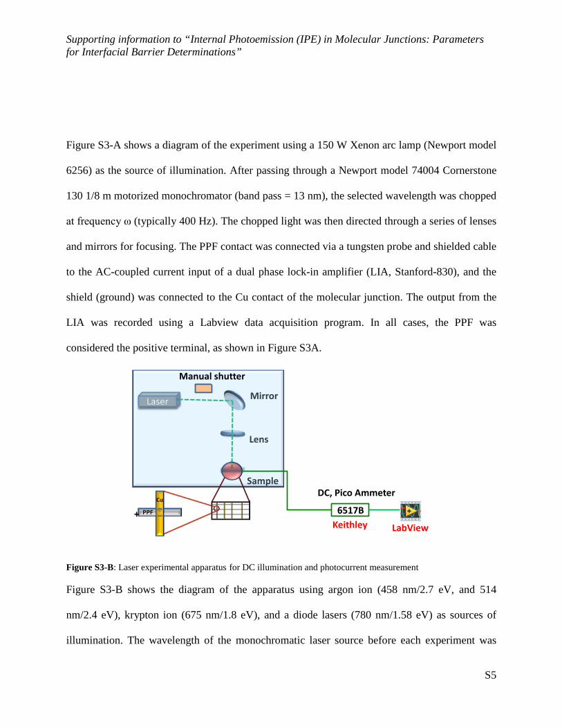
Figure S3-B: Laser experimental apparatus for DC illumination and photocurrent measurement
Figure S3-B shows the diagram of the apparatus using argon ion (458 nm/2.7 eV, and 514
nm/2.4 eV), krypton ion (675 nm/1.8 eV), and a diode lasers (780 nm/1.58 eV) as sources of
illumination. The wavelength of the monochromatic laser source before each experiment was
Mirror
Lens
Sample
+
Manual shutter
6517BKeithley LabView
DC, Pico Ammeter
Supporting information to “Internal Photoemission (IPE) in Molecular Junctions: Parameters for Interfacial Barrier Determinations”
S6
verified using an Ocean Optics spectrometer (USB-4000). The power from the laser beam at the
sample was determined using a power meter directly above the sample before and after each
experiment. For all the experiments carried out in this study, the intensity of the laser beam was
varied between 1 and 50 mW, with a focused spot size of ~1 mm. A manual shutter was used to
control exposure time. The PPF contact was contacted with a tungsten probe and connected to
the input of a DC picoammeter (Kiethley 6517B) to read the photocurrent, and the output from
the picommeter was recorded using a Labview data acquisition program. 808 nm and 852 nm
Fabry-Perot laser diodes from Thorlabs were capable of 100 mW output each. A Thorlabs LDC
210C laser diode controller and a TED 200C thermoelectric temperature controller were used to
drive and control laser output.
4. Method for determining Absorption spectra
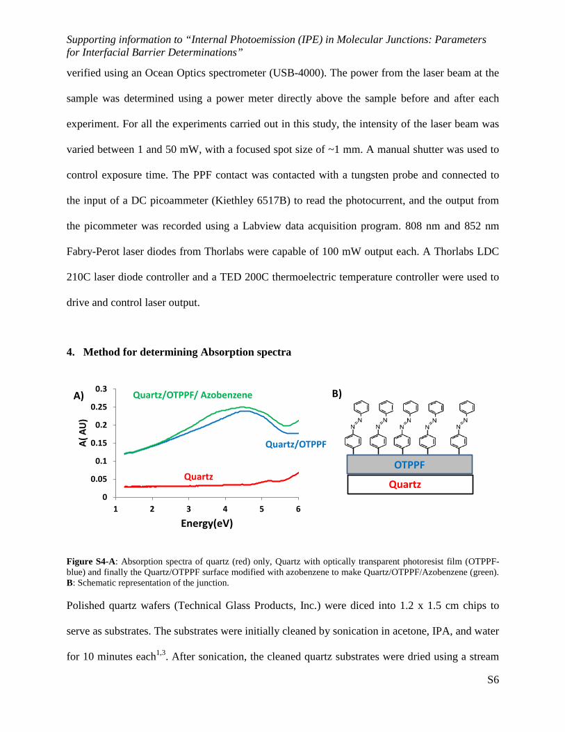
Figure S4-A: Absorption spectra of quartz (red) only, Quartz with optically transparent photoresist film (OTPPF-blue) and finally the Quartz/OTPPF surface modified with azobenzene to make Quartz/OTPPF/Azobenzene (green). B: Schematic representation of the junction.
Polished quartz wafers (Technical Glass Products, Inc.) were diced into 1.2 x 1.5 cm chips to
serve as substrates. The substrates were initially cleaned by sonication in acetone, IPA, and water
for 10 minutes each1,3. After sonication, the cleaned quartz substrates were dried using a stream
Quartz/OTPPF
0
0.05
0.1
0.15
0.2
0.25
0.3
1 2 3 4 5 6
A( A
U)
Energy(eV)
Quartz
Quartz/OTPPF/ AzobenzeneA)
Quartz
OTPPF
B)

Supporting information to “Internal Photoemission (IPE) in Molecular Junctions: Parameters for Interfacial Barrier Determinations”
S7
of N2 gas. The absorption spectra of each quartz substrate (with an air reference) were obtained
using a Perkin Elmer 900 spectrometer. The red curve in Figure S4-A shows the absorbance of a
typical quartz substrate. After obtaining the spectrum for each quartz substrate, a commercially-
available photoresist (AZ-P4330-RS) was diluted (5 % by volume) using propylene glycol
methyl ether acetate, then this solution was spin coated onto quartz slides at 6000 rpm for 60
sec4. After soft baking at 90oC for 10 min, samples were transferred to a tube furnace for
pyrolysis. Forming gas (5% H2 in N2) was kept flowing at 100 sccm throughout pyrolysis, during
which the temperature was ramped at 10o C/min up to 1025 °C for 1 hour, as reported
elsewhere3,4, resulting in an optically-transparent pyrolyzed photoresist film. The absorption
spectra of the optically transparent PPF (OTPPF) films were then obtained, with a typical result
shown in Figure S4-A, blue curve. Finally the OTPPF substrate was modified with molecular
layers ranging from 1 to 5 nm in thickness using electrochemical reduction of diazonium salts in
solution as reported elsewhere4. An example of the absorbance spectrum obtained for a layer of
azobenzene on OTPPF is shown in Figure S4-A, green curve. Figure S4-A shows all three
absorption curves for each component of the sample taken at different times during fabrication.
Figure S4-B shows a schematic of a completed sample.
Figure S4-C: Absorption spectrum of Azobenzene (3.4 nm) obtained from the spectra of figure S4A.
-0.01
0
0.01
0.02
0.03
0.04
1 2 3 4 5 6
A (A
U)
Energy (eV)
Azobenzene Absorption - subtracted
Abs Q/OTPPF/molecule – Abs Q/OTPPF = Abs molecule

Supporting information to “Internal Photoemission (IPE) in Molecular Junctions: Parameters for Interfacial Barrier Determinations”
S8
In order to obtain the absorption spectrum for a molecular layer, the absorbance obtained from an
unmodified quartz/carbon substrate (described above) is subtracted from that for the same
sample following modification by the molecular layer (i.e., quartz/OTPFF/AB). The result is
shown in Figure S4-C. The small negative absorbance is due to the refractive index change
between the reference (unmodified transparent carbon) and the sample upon addition of the thin
molecular layer.
5. Optical absorption spectra for different molecules:
Figure S5-A: Optical absorption spectra C12, AQ, AB, NAB, and BrP following subtraction of
OTPPF spectrum. B: Method for determining onset of optical absorption.
Figure S5-A shows the overlay of optical absorption spectra for the different molecules used in
this study using the procedure outlined above. The onset of absorption by molecular layer is
taken as the intersection of two linear regions of the corrected spectrum as shown in figure S5B.
The optical absorption onset for thus determined was 1.7 eV (AB and NAB), 2.5 eV (AQ) and
3.6eV (BrP, as reported in the main text Table 1.
-0.01
0
0.01
0.02
0.03
0.04
1.4 2.4 3.4 4.4
A (A
U)
Energy (eV)
AQ
AB
C12
NABBrP
A)
-0.003
0
0.003
0.006
1.4 2.4 3.4 4.4
A (A
U)
Energy (eV)
AQAB
NABBrP
2.5 eV 3.6eV
B)
1.7 eV
1.7eV

Supporting information to “Internal Photoemission (IPE) in Molecular Junctions: Parameters for Interfacial Barrier Determinations”
S9
6. Excitation intensity profiles for alkanes:
Figure S6: Photocurrent vs. intensity for an alkane junction at 2.4 eV (458 nm) and 2.7 eV (516 nm).
Figure S6 shows the photocurrent as a function of excitation intensity for alkane junctions for
two different energies (2.4 and 2.7 eV). The linearity of the curves shows that the photocurrent is
controlled by monomolecular recombination.
Table S1 lists the correlation coefficient (R2) determined from linear (Iphoto vs. Intensity) or
quadratic [(Iphoto)2 vs Intensity] plots of photocurrent vs incident light intensity in Watts. NDI, Fc,
BrP, AQ and alkane junctions more closely fit a linear function of intensity at 2.7 and 2.4 eV,
while AB has a better fit to a quadratic function at either 2.4 or 1.9 eV. Photocurrent vs. intensity
curves for the alkane are in Figure S6, and those for all other molecules are provided in the main
text.
Alkane
y = 3.9949x + 2.7743R² = 0.9943
y = 2.9926x + 2.992R² = 0.993
0
10
20
30
40
50
60
0 5 10 15
i p(n
A)
Incident Power (mW)
2.41eV
2.7eV
A)

Supporting information to “Internal Photoemission (IPE) in Molecular Junctions: Parameters for Interfacial Barrier Determinations”
S10
Table S1: R2 correlation coefficient for both Iphoto vs. incident power and the (Iphoto)2 vs. the
incident power for all molecular junctions in this study.
7. Structure and absorption spectra for NDI and ferrocene molecular layers:
Figure S7: Absorption spectra of Fc (A) and NDI (B) films on OTPPF (both NDI & Fc are 3-
4nm thick), after subtraction of the OTPPF spectrum
NDIGraph R2 fitting
value (2.7eV)R2 fitting
Value (2.4eV)
I photo Vs incident power
0.9899 0.9893
(I photo )2 Vs incident power
0.9552 0.9819
Graph R2 fittingvalue (2.4eV)
R2 fitting Value (1.9eV)
I photo Vs incident power
0.9966 0.9967
(I photo )2 Vs incident power
0.944 0.9073
Fc
Graph R2 fittingvalue (2.4eV)
R2 fitting Value (2.7eV)
I photo Vs incident power
0.9917 0.9946
(I photo )2 Vs incident power
0.9646 0.9696
BrP
Graph R2 fittingvalue (2.4eV)
R2 fitting Value (1.9eV)
I photo Vs incident power
0.9638 0.9653
(I photo )2 Vs incident power
0.998 0.9937
AB
Graph R2 fittingvalue (2.4eV)
R2 fitting Value (2.7eV)
I photo Vs incident power
0.9943 0.993
(I photo )2 Vs incident power
0.9646 0.9692
Alkane
Graph R2 fittingvalue (2.4eV)
R2 fittingvalue (1.8eV)
I photo Vs incident power
0.9952 0.9981
(I photo )2 Vs incident power
0.9314 0.9728
AQ
-0.02
0
0.02
0.04
0.06
1.5 2.5 3.5 4.5
Abso
rban
ce
Energy(eV)
Fe
NH2PPF
A)
-0.03
0
0.03
0.06
0.09
0.12
1.5 2.5 3.5 4.5
Abs
orb
ance
Energy(eV)
N
N
O O
O O
NH2PPF
B)

Supporting information to “Internal Photoemission (IPE) in Molecular Junctions: Parameters for Interfacial Barrier Determinations”
S11
Figure S7-A shows the optical absorption spectrum for Ferrocene (Fc) with an inset showing
schematic structure of Fc molecule on the carbon surface. Figure S8-B shows the optical
absorption spectrum of NDI with inset showing its structure. The optical absorption spectrum for
each molecule was obtained from the procedure of section 4 above.
8. Yield vs. molecular layer thickness plots:
Yield vs. molecular layer thickness plots for AB, NAB, NDI and Fc are shown in figure S8. As
noted in the main text, the thickness dependence is much larger when the molecular layer
absorbs light.
Figure S8: Yield vs. thickness plot of Fc, NDI, AB and NAB used in the study
-2.50E-04
-1.50E-04
-5.00E-05
5.00E-053 3.5 4 4.5
Y(e-
/pho
ton)
Thickness-NAB(nm)
1.82 eV
3.26 eV
-1.E-04
-1.E-04
-6.E-05
-2.E-05
2.E-051.5 2.5 3.5 4.5
Y(e-
/pho
ton)
Thickness AB(nm)
3.26 eV
1.82 eV
0.E+00
1.E-05
2.E-05
3.E-05
2.5 3 3.5 4 4.5 5
Y (e
-/ph
oton
)
Thickness(nm)
Ferrocene
A
1.82 eV
3.26 eV
-2.E-04
-2.E-04
-8.E-05
0.E+002.5 3 3.5 4 4.5
Y(e-
/pho
ton)
Thickness(nm)
NDI
B
1.82 eV
3.26 eV
C D

Supporting information to “Internal Photoemission (IPE) in Molecular Junctions: Parameters for Interfacial Barrier Determinations”
S12
9. Fowler Plots:
Figure S9 shows the Fowler plots for all the molecules studied. The error bars show the standard
deviation of photocurrent for four different junctions on the same sample. Table S2 shows the
value of Fowler intercepts obtained from the Fowler plots, and they are provided in the main
text, table 2 The intercepts and their errors were determined statistically using standard methods5
as follows. Let xi represent photon energy yi represent Y1/2, A the y-axis intercept of the Y1/2 vs.
photon energy plot, B the associated slope, and σA the error of the intercept on the ordinate.
𝐴 = ∑𝑥2 ∑𝑦− ∑𝑥∑𝑥𝑦∆
(S1)
𝐵 = 𝑁∑𝑥𝑦− ∑𝑥∑𝑦∆
(S2)
∆ = 𝑁∑𝑥2 − (∑𝑥)2 (S3)
𝜎𝑦 = � 1𝑁−2
∑ (𝑦𝑖 − 𝐴 − 𝐵𝑥𝑖)2𝑁𝑖=1 (S4)
𝜎𝐴 = 𝜎𝑦�∑𝑥2
∆ (S5)
𝜎𝐵 = 𝜎𝑦�𝑁∆ (S6)
The Fowler intercept on the photon energy axis is the absolute value of A/B, and the error on this
intercept (σFowler ) is determined by equation S7.
σFowler = � A B� � σB
|B| + σA|A|� (S7)
The values obtained from this equation are given in table S2:

Supporting information to “Internal Photoemission (IPE) in Molecular Junctions: Parameters for Interfacial Barrier Determinations”
S13
Figure S9: Fowler plots for BrP, NDI, Fc, AQ and AB.
Table S2: Fowler intercepts for each molecule along with their errors.
a- Approximate, based on two points (808 and 852 nm), insufficient data points to calculate the error for intercept.
b- NAB does not meet the criteria for IPE; therefore the Fowler intercept is not relevant.
References
(1) Ranganathan, S.; McCreery, R. L. Anal. Chem. 2001, 73, 893. (2) Fereiro, J. A.; McCreery, R. L.; Bergren, A. J. Journal of the American Chemical
Society 2013, 135, 9584.
0
0.002
0.004
0.006
0.008
0.01
1 1.4 1.8 2.2 2.6 3
Y1/2
(e- /
phot
on)
Energy (eV)
BrP
Fc, AQ
-0.002
-0.0016
-0.0012
-0.0008
-0.0004
0
Y 1/
2(e
-/ph
oton
)
NDI
A
-0.003
-0.0025Y
0
0.001
0.002
0.003
0.004
Y1/
2 (e
-/ph
oton
)
Energy, eV
AB
AB
Junction Fowler intercept σ Fowler
BrP (3.0nm) 1.10 eV 0.11 eV
AQ (3.3nm) 1.65 eV 0.10 eV
AB a (3.4nm) 0.9eV -
NAB b (3.3nm) <1.4eV -
Fc (4.0nm) 1.60eV 0.15 eV
NDI (3.5nm) 1.40eV 0.30 eV

Supporting information to “Internal Photoemission (IPE) in Molecular Junctions: Parameters for Interfacial Barrier Determinations”
S14
(3) Ranganathan, S.; McCreery, R. L.; Majji, S. M.; Madou, M. J. Electrochem. Soc. 2000, 147, 277.
(4) Tian, H.; Bergren, A. J.; McCreery, R. L. Applied Spectroscopy 2007, 61, 1246. (5) Taylor, J. R. An Introduction to Error Analysis: The Study of Uncertainties in
Physical Measurements; 2nd ed.; University Science Books: Sausalito, California, 1997, pp. 182-190