Embed Size (px)
Citation preview

Supporting Information
for
Intrinsic ultrasmall nanoscale silicon turns n-/p-type with SiO2/Si3N4-
coating
Dirk König∗1, 2, Daniel Hiller2, 3, Noël Wilck4, Birger Berghoff4, Merlin Müller5, Sangeeta Thakur6,
Giovanni Di Santo6, Luca Petaccia6, Joachim Mayer5, Sean Smith1, 7 and Joachim Knoch4
Address: 1Integrated Materials Design Centre, University of New South Wales, NSW 2052, Aus-
tralia; 2Laboratory of Nanotechnology, Dept. of Microsystems Engineering (IMTEK), University of
Freiburg, 79110, Germany; 3Research School of Engineering, The Australian National University,
ACT 2601, Australia; 4Institute of Semiconductor Electronics (IHT), RWTH Aachen University,
52074, Germany; 5Ernst-Ruska Centre for Microscopy and Spectroscopy with Electrons, RWTH
Aachen University, 52074, Germany; 6Elettra Sincrotrone Trieste, Strada Statale 14 km 163.5, 34149
Trieste, Italy and 7National Compute Infrastructure (NCI), The Australian National University, ACT
2601, Australia
Email: Dirk König - [email protected]
∗ Corresponding author
Further discussion and data of h-DFT, UPS, and NEGF simulations
Comparison of h-DFT Approximants to Experimental Data
We evaluate h-DFT calculations with identical compute algorithms as decribed in the main publica-
tion using approximants presenting pure dielectrics (SiO2, Si3N4). Such approximants establish the
base for a comparison with respective experimental bulk phase data. Si-NCs embedded in SiO2 or
Si3N4 do not present a good basis for comparison due to size distributions of Si-NCs and associated
distributions in mechanical stress in experimental samples. Due to the wider distribution of bond
lengths and angles, the calculation of amorphous SiO2- and Si3N4-phases would require approxi-
mants in the range of at least 50,000 atoms to provide the statistical information (main value, stan-
dard deviation, skewness) for comparison with experiment. With the accurate h-DFT methods used
here, the computation effort goes far beyond the feasible limit. We therefore resort to experimental
data of the respective crystalline phase and show that our calculations closely match morphological
and electronic experimental data of the respective dielectric bulk phase, underlining their accuracy
and predictive power.
Morphology
The 3-21G Gaussian type MO-BS [1,2] used with the HF method delivers good accuracies for the
structural optimization [3-6] and presents the optimum compromise between ultimate accuracy and
tractable real-space computation for very large approximants such as the Si165(NH2)100 (465 atoms)
nanocrystal (NC) or the Si233(OH)81(NH2)87 NWire (718 atoms). For approximants with ground
state HOMO–LUMO gaps above a certain threshold, the error in correlation forces is small for the
occupied states due to their strong localization [7]. This threshold of the HOMO–LUMO gap for
inorganic crystallites was found to be < 1.3 eV by results from numerous Si- and Ge-based approx-
imants matching experimental band gap values [8]. On the other hand, exact exchange interaction is
inherent to HF methods which is important for localized electron pairs as in atomic bonds [7].
For structural comparison we focus on Si29O76H36 and Si40N86H96 approximants presenting sto-
ichiometric bulk phases of SiO2 (α-quartz) and Si3N4 (α-phase), respectively, if we consider
each H-atom as 1/4 Si. With this assumption, we get Si38O76 = 38 SiO2 formula units and
S2

Si64N86 = 21 13 Si3N4 formula units plus 2 N, resulting in Si3N4.03. Such approximants do not in-
clude structural deviations caused by local stress due to interfacing to Si-NCs or the other respec-
tive dielectric. Both approximants underwent structural optimization with the HF/3-21G and the
B3LYP/6-31G(d) route. By computing approximants which contain one or two Si10 NCs with the
HF/3-21G // B3LYP/6-31G(d) route, their results can be compared to each other as well as to earlier
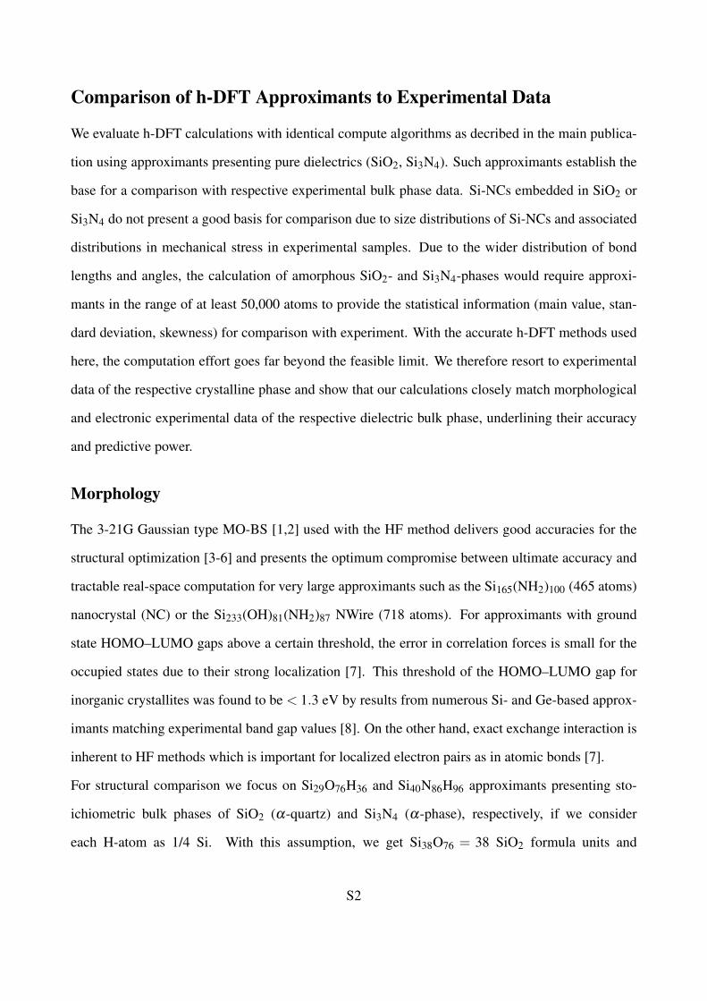
works of OH-terminated Si-NCs [4,5,9-11]. Both approximants are shown in Fig. S1.
Figure S1: Si29O76H36 and Si40N86H96 approximants presenting SiO2 (α-quartz) and α-Si3N4. Theapproximants are shown in the respective geometry after structural optimization with the B3LYPhybrid DF and a 6-31G(d) MO-BS. Structural differences to approximants optimized with the HFapproach and a 3-21G MO-BS are difficult to spot solely by imaging, cf. Tables S1 and S2.
We compare the bond lengths aSi−X (X = O, N) and bond angles αSi−X−Si of the two different
optimization routes with experimental results and start with the Si29O76H36 approximant describing
SiO2.
Table S1 shows the average and standard deviation of aSi−O and αSi−O−Si. Bonds to OH groups
as outermost termination of the approximant were not included. These bond lengths have an av-
erage aSi−OH = 1.620 Å and a standard deviation of σ(aSi−OH) = 0.013 Å for the HF/3-21G op-
timization route. The higher level B3LYP/6-31G(d) optimization yielded aSi−OH = 1.647 Å and
σ(aSi−OH) = 0.013 Å. The average bond lengths of Si to OH groups is only 0.5% and 0.7% larger
as compared to aSi−O of the HF/3-21G and B3LYP/6-31G(d) optimization, respectively. Referring
S3
to bond geometry, this is a clear indication that the H termination of the outermost O atoms is an
accurate approximation of an O–Si≡ bond.
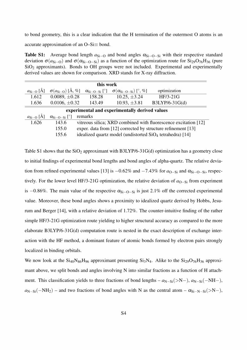
Table S1: Average bond length aSi−O and bond angles αSi−O−Si with their respective standarddeviation σ(aSi−O) and σ(αSi−O−Si) as a function of the optimization route for Si29O76H36 (pureSiO2 approximants). Bonds to OH groups were not included. Experimental and experimentallyderived values are shown for comparison. XRD stands for X-ray diffraction.
this workaSi−O [Å] σ(aSi−O) [Å, %] αSi−O−Si [◦] σ(αSi−O−Si) [◦, %] optimization
1.612 0.0089, ±0.28 158.28 10.25, ±3.24 HF/3-21G1.636 0.0106, ±0.32 143.49 10.93, ±3.81 B3LYP/6-31G(d)
experimental and experimentally derived valuesaSi−O [Å] αSi−O−Si [◦] remarks
1.626 143.6 vitreous silica; XRD combined with fluorescence excitation [12]155.0 exper. data from [12] corrected by structure refinement [13]155.6 idealized quartz model (undistorted SiO4 tetrahedra) [14]
Table S1 shows that the SiO2 approximant with B3LYP/6-31G(d) optimization has a geometry close
to initial findings of experimental bond lengths and bond angles of alpha-quartz. The relative devia-
tion from refined experimental values [13] is −0.62% and −7.43% for aO−Si and αSi−O−Si, respec-
tively. For the lower level HF/3-21G optimization, the relative deviation of aO−Si from experiment
is −0.86%. The main value of the respective αSi−O−Si is just 2.1% off the corrected experimental
value. Moreover, these bond angles shows a proximity to idealized quartz derived by Hobbs, Jesu-
rum and Berger [14], with a relative deviation of 1.72%. The counter-intuitive finding of the rather
simple HF/3-21G optimization route yielding to higher structural accuracy as compared to the more
elaborate B3LYP/6-31G(d) computation route is nested in the exact description of exchange inter-
action with the HF method, a dominant feature of atomic bonds formed by electron pairs strongly
localized in binding orbitals.
We now look at the Si40N86H96 approximant presenting Si3N4. Alike to the Si29O76H36 approxi-
mant above, we split bonds and angles involving N into similar fractions as a function of H attach-
ment. This classification yields to three fractions of bond lengths – aN−Si(>N−), aN−Si(−NH−),
aN−Si(−NH2) – and two fractions of bond angles with N as the central atom – αSi−N−Si(>N−),
S4
αSi−N−Si(−NH−). Main values and standard deviations of all aN−Si(>N−) and aN−Si(−NH−) as
well as all αSi−N−Si(>N−) and αSi−N−Si(−NH−) relevant for pure Si3N4 are listed in Table S2.
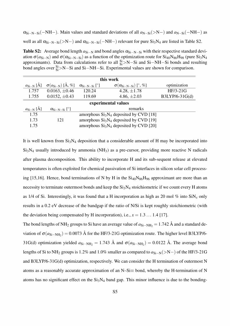
Table S2: Average bond length aSi−N and bond angles αSi−N−Si with their respective standard devi-ation σ(aSi−N) and σ(αSi−N−Si) as a function of the optimization route for Si40N86H98 (pure Si3N4approximants). Data from calculations refer to all Si
Si>N−Si and Si−NH−Si bonds and resultingbond angles over Si
Si>N−Si and Si−NH−Si. Experimental values are shown for comparison.
this workaSi−N [Å] σ(aSi−N) [Å, %] αSi−N−Si [◦] σ(αSi−N−Si) [◦, %] optimization
1.757 0.0163, ±0.46 120.24 4.28, ±1.78 HF/3-21G1.755 0.0152, ±0.43 119.69 4.86, ±2.03 B3LYP/6-31G(d)
experimental valuesaSi−N [Å] αSi−N−Si [◦] remarks
1.75 amorphous Si3N4 deposited by CVD [18]1.73 121 amorphous Si3N4 deposited by CVD [19]1.75 amorphous Si3N4 deposited by CVD [20]
It is well known from Si3N4 deposition that a considerable amount of H may be incorporated into
Si3N4 usually introduced by ammonia (NH3) as a pre-cursor, providing more reactive N radicals
after plasma decomposition. This ability to incorporate H and its sub-sequent release at elevated
temperatures is often exploited for chemical passivation of Si interfaces in silicon solar cell process-
ing [15,16]. Hence, bond terminations of N by H in the Si40N86H96 approximant are more than an
necessity to terminate outermost bonds and keep the Si3N4 stoichiometric if we count every H atoms
as 1/4 of Si. Interestingly, it was found that a H incorporation as high as 20 mol % into SiNx only
results in a 0.2 eV decrease of the bandgap if the ratio of N/Si is kept roughly stoichiometric (with
the deviation being compensated by H incorporation), i.e., x = 1.3 . . . 1.4 [17].
The bond lengths of NH2 groups to Si have an average value of aSi−NH2 = 1.742 Å and a standard de-
viation of σ(aSi−NH2) = 0.0073 Å for the HF/3-21G optimization route. The higher level B3LYP/6-
31G(d) optimization yielded aSi−NH2 = 1.743 Å and σ(aSi−NH2) = 0.0122 Å. The average bond
lengths of Si to NH2 groups is 1.2% and 1.0% smaller as compared to aSi−N(>N−) of the HF/3-21G
and B3LYP/6-31G(d) optimization, respectively. We can consider the H termination of outermost N
atoms as a reasonably accurate approximation of an N–Si≡ bond, whereby the H-termination of N
atoms has no significant effect on the Si3N4 band gap. This minor influence is due to the bonding-
S5
antibonding MO splitting being significantly bigger for the H–N bond than the Si–N bond. The
situation improves greatly for the bond lengths of –NH– groups. We get aSi−NH−Si = 1.749 Å and
a standard deviation of σ(aSi−NH−Si) = 0.0133 Å for the HF/3-21G optimization route. The higher
level B3LYP/6-31G(d) optimization yielded aSi−NH−Si = 1.745 Å and σ(aSi−NH−Si) = 0.0135 Å.
The deviation of aSi−NH−Si from the average of the experimental values in Table S2 – aN−Si = 1.743
Å – is merely 0.31% for the HF/3-21G route (0.11% for B3LYP/6-31G(d) route). This is an indica-
tion that NH2 groups do not exist in real Si3N4 and virtually all incorporated H bond to N is attached
to –N– bridging two Si atoms. We can derive from this finding that for Si3N4.2:H [17], about 20%
of N atoms exists in this –NH– bridging configuration. The values of Si−N bond lengths for fully
Si-terminated N are 1.07% (1.01%) larger for the HF/3-21G (B3LYP/6-31G(d) ) route as compared
to the average of experimental values of 1.743 Å obtained from data in Table S2. For the cumulative
value of bond lengths aSi−Nall , we do not consider the bonds Si−NH2 as they do not appear to exist
in Si3N4 and Si3Nx:H. We then get aSi−Nall = aSi−NH−Si + aSi−N(>N−) = 1.757 Å for the HF/3-
21G route (1.755 Å for the B3LYP/6-31G(d) route), see Table S2. Such values are 0.78% (0.67%)
bigger as compared to the average of the experimental values in Table S2 = 1.743 Å, showing a high
accuracy in structural optimization. Here, the higher level B3LYP/6-31G(d) optimization route is
slightly more accurate regarding bond lengths.
Results on Si–N–Si bond angles favour the HF-3-21G route when compared to the experimen-
tal value of αSi−N−Si = 121.0◦; the deviation is −1.78◦ or −0.98% (−2.21◦ or −1.83% for the
B3LYP/6-31G(d) route). If angles of the form Si−NH−Si are included into the analysis, we get
αSi−N−Si = 120.24± 2.14◦ for the HF/3-21G route (αSi−N−Si = 119.69± 2.43◦ for the B3LYP/6-
31G(d) route), whereby the ± tolerance stands for the standard deviation, cf. Table S2. This cu-
mulative value diminishes the error to experiment down to −0.76◦ or −0.63% (−1.31◦ or −1.08%
for the B3LYP/6-31G(d) route). In both cases, the calculated values of αSi−N−Si are very close to
experiment, with the HF/3-21G route having an edge over the more costly B3LYP/6-31G(d) route.
Considering angles of the Si–NH–Si bonds in addition to SiSi>N–Si bonds is the more realistic option
due to the existence of significant amounts of H in CVD-deposited Si3N4, see above.
S6

Electronic Structure
Approximants were calculated using the HF/3-21G // B3LYP/6-31G(d), the B3LYP/6-31G(d) //
B3LYP/6-31G(d) and the B3LYP/6-31G(d) // B3LYP/6-31+G(d) route. The latter was chosen in
order to elucidate the impact of the different optimization methods onto the electronic structure. It
also enables us to evaluate the impact of the diffuse primitive Gaussian functions on the electronic
structure.
In real-space DFT calculations, the exact calibration to an absolute energy scale (the vacuum level
Evac) is known to be ambiguous [21]. Nevertheless, relative changes of energy values such as band
offsets or fundamental energy gaps between approximants with different interface termination are
accurate within the same computation route. Therefore, the results of the production runs obtained
with the HF/3-21G(d)//B3LYP/6-31G(d) route are accurate apart from a constant offset for all MO
energies and hence trustworthy. As a consequence, all energy-dependent results are accurate within
the same real-space DFT//MO-Basis-Set method and can be compared with experimental data on a
relative base such as ∆E between SiO2- and Si3N4-coated Si-NWire-sections or electronic gaps [22].
For the Si29O76H36 approximant, we see that the band gap is underestimated for all DFT methods
used. However, experimental values of Egap of thin thermal SiO2 layers formed by oxidizing Si
wafers vary considerably from 8.0 to 8.9 eV, while bulk forms of SiO2 have even lower values, see
to bottom of Table S3. The rather wide range of experimental values for the fundamental gap of
SiO2 add to the complexity of a quantitative evaluation of DFT results against experiment. The best
result is obtained once again with the HF/3-21G // B3LYP/6-31G(d) route since it gets closest to the
range of experimental Egap values.
For Si3N4 we presume an experimental value of Egap(Si3N4) = 5.4 eV which results from the aver-
age of experimental findings in Table S4. The DFT results of the Si40N86H98 approximant show that
the HF/3-21G // B3LYP/6-31G(d) route is slightly more accurate (rel. error =+10.1%) as compared
to the B3LYP/6-31G(d) // B3LYP/6-31G(d) route (rel. error = +11.4%). While the better accuracy
in the electronic structure for a lower level optimization may be counter-intuitive, we note that the
advantages of the HF method for structural optimization as discussed above have far-reaching con-
S7
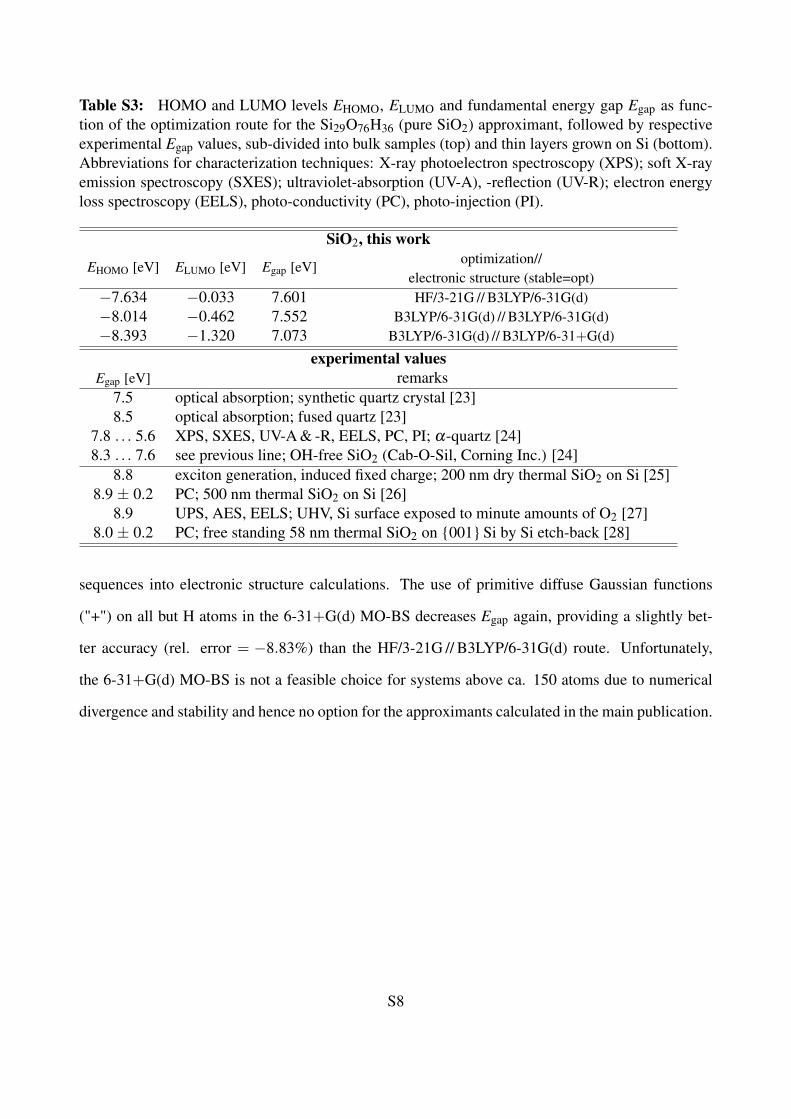
Table S3: HOMO and LUMO levels EHOMO, ELUMO and fundamental energy gap Egap as func-tion of the optimization route for the Si29O76H36 (pure SiO2) approximant, followed by respectiveexperimental Egap values, sub-divided into bulk samples (top) and thin layers grown on Si (bottom).Abbreviations for characterization techniques: X-ray photoelectron spectroscopy (XPS); soft X-rayemission spectroscopy (SXES); ultraviolet-absorption (UV-A), -reflection (UV-R); electron energyloss spectroscopy (EELS), photo-conductivity (PC), photo-injection (PI).
SiO2, this workoptimization//EHOMO [eV] ELUMO [eV] Egap [eV]
electronic structure (stable=opt)−7.634 −0.033 7.601 HF/3-21G // B3LYP/6-31G(d)−8.014 −0.462 7.552 B3LYP/6-31G(d) // B3LYP/6-31G(d)−8.393 −1.320 7.073 B3LYP/6-31G(d) // B3LYP/6-31+G(d)
experimental valuesEgap [eV] remarks
7.5 optical absorption; synthetic quartz crystal [23]8.5 optical absorption; fused quartz [23]
7.8 . . . 5.6 XPS, SXES, UV-A & -R, EELS, PC, PI; α-quartz [24]8.3 . . . 7.6 see previous line; OH-free SiO2 (Cab-O-Sil, Corning Inc.) [24]
8.8 exciton generation, induced fixed charge; 200 nm dry thermal SiO2 on Si [25]8.9 ± 0.2 PC; 500 nm thermal SiO2 on Si [26]
8.9 UPS, AES, EELS; UHV, Si surface exposed to minute amounts of O2 [27]8.0 ± 0.2 PC; free standing 58 nm thermal SiO2 on {001} Si by Si etch-back [28]
sequences into electronic structure calculations. The use of primitive diffuse Gaussian functions
("+") on all but H atoms in the 6-31+G(d) MO-BS decreases Egap again, providing a slightly bet-
ter accuracy (rel. error = −8.83%) than the HF/3-21G // B3LYP/6-31G(d) route. Unfortunately,
the 6-31+G(d) MO-BS is not a feasible choice for systems above ca. 150 atoms due to numerical
divergence and stability and hence no option for the approximants calculated in the main publication.
S8
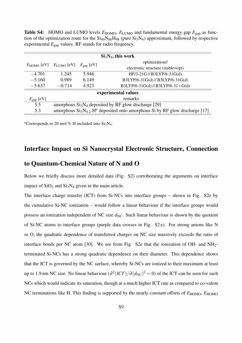
Table S4: HOMO and LUMO levels EHOMO, ELUMO and fundamental energy gap Egap as func-tion of the optimization route for the Si40N86H98 (pure Si3N4) approximant, followed by respectiveexperimental Egap values. RF stands for radio frequency.
Si3N4, this workoptimization//EHOMO [eV] ELUMO [eV] Egap [eV]
electronic structure (stable=opt)−4.701 1.245 5.946 HF/3-21G // B3LYP/6-31G(d)−5.160 0.989 6.149 B3LYP/6-31G(d) // B3LYP/6-31G(d)−5.637 −0.714 4.923 B3LYP/6-31G(d) // B3LYP/6-31+G(d)
experimental valuesEgap [eV] remarks
5.5 amorphous Si3N4 deposited by RF glow discharge [29]5.3 amorphous Si3N4.2:Ha deposited onto amorphous Si by RF glow discharge [17]
aCorresponds to 20 mol % H included into Si3N4.
Interface Impact on Si Nanocrystal Electronic Structure, Connection
to Quantum-Chemical Nature of N and O
Below we briefly discuss more detailed data (Fig. S2) corroborating the arguments on interface
impact of SiO2 and Si3N4 given in the main article.
The interface charge transfer (ICT) from Si-NCs into interface groups – shown in Fig. S2e by
the cumulative Si-NC ionization – would follow a linear behaviour if the interface groups would
possess an ionization independent of NC size dNC. Such linear behaviour is shown by the quotient
of Si-NC atoms to interface groups (purple data crosses in Fig. S2 e). For strong anions like N
or O, the quadratic dependence of transferred charges on NC size massively exceeds the ratio of
interface bonds per NC atom [30]. We see from Fig. S2e that the ionization of OH- and NH2-
terminated Si-NCs has a strong quadratic dependence on their diameter. This dependence shows
that the ICT is governed by the NC surface, whereby Si-NCs are ionized to their maximum at least
up to 1.9 nm NC size. No linear behaviour (∂ 2(ICT )/∂ (dNC)2 = 0) of the ICT can be seen for such
NCs which would indicate its saturation, though at a much higher ICT rate as compared to co-valent
NC terminations like H. This finding is supported by the nearly constant offsets of EHOMO, EHOMO
S9

Figure S2: h-DFT Simulation results of Silicon Nanocrystals (Si-NCs). Si-NCs of 1.9 nm sizefully terminated with OH groups – Si165(OH)100 (a) – and NH2 groups – Si165(OH)100 (b) – afterstructural optimization, seen along 〈110〉 axis to illustrate {111} faceting. Si atom colour is grey,O is red, N is blue and H is white. (c) HOMO and LUMO energy positions referring to vacuumlevel and (d) resulting fundamental gap of Si-NCs as function of interface termination over NC size.(e) Total Si-NC ionization and ratio of interface groups per Si-NC atom [30] as function of interfacetermination over NC size.
and Egap between OH- and NH2-terminated Si-NCs over dNC (Fig. S2c,). Geometrical arguments
[22] show that the saturation of the ICT occurs at NC sizes > 7 nm. In this context, we point out that
the octahedral {111}-faceted Si-NCs have a maximum value of the ratio of NC atoms per interface
group as compared to other Si-NCs [30] which leads to the earliest onset of ICT saturation. As a
consequence, less symmetric Si-NCs like fin-field-effect transistors (FETs) will have their electronic
structure dominated by the ICT to far bigger structure sizes [30].
S10
Normalization of UPS Scans With Further Reference Data
Normalization
Before features such as material-characteristic valence band edges or highest occupied states (HOS)
of NWells can be quantitatively evaluated on an energy scale, UPS scans have to get normalized.
The normalization of UPS signals has to be carried out at an electron kinetic energy Ekin where
there are no occupied states and the only contributions to the resulting background signal are
events which are comparatively rare to the fundamental photonic excitation of electrons in occu-
pied states. Such processes are free carrier re-absorption and multiple carrier inelastic scattering of
primary electrons with high energy secondary electrons and/or other primary electrons [32]. Since
a maximum energetic distance of the excited electrons from their origin energy (HOS) enables a
maximum de-coupling of the UPS signal from the background, we chose the kinetic energy range
Ekin = [hν ;hν−0.5 eV]. Normalization is then carried out as follows:
1. All UPS scans are brought onto the same average intensity (counts per second [cps]) in the
energy range considered (dash-dotted rectangle in Fig. S3) which requires a weighting factor
per scan. This factor is set to one for the reference (Ref-Si-wafer). With the weighting factors,
the resulting average cps value is then valid for all samples.
2. The cps offset from zero – here it is 60 cps (dash-dotted line in Fig. S3) – is then substrated
from all UPS scans.
The procedure is analog for SiO2 and Si3N4 reference samples but on a different Ekin scale due to
their different hν . The scans of these reference samples were normalized to the Si reference in the
same manner as explained above using Ekin = [hν ;hν − 0.5 eV] = [20.0; 19.5] eV, allowing for a
direct comparison on an energy scale relating to Evac (Fig. S4e).
Data of SiO2 and Si3N4 Reference Samples
The valence band energies EV of SiO2 and Si3N4 are located considerably deeper below the vacuum
level Evac as compared to the Si-based samples in the main publication, requiring a higher UV photon
S11

5.0 5.5 6.0 6.5 7.0 7.5 8.0 8.50
60
120
180
240
300 QW-17-N QW-26-N QW-17-O Ref-Si-wafer
h = 8.9 eV
norm
aliz
ed c
ps
Ekin [eV]
Figure S3: Normalization of UPS signals to enable quantitative comparison of different scansrecorded with the same UV photon energy E(hν). Data of NWell samples and H-terminated Siwafer as reference for Si NWells are shown here. These scans get assessed at the high end of Ekinrange - Ekin = [hν ;hν−0.5 eV], dash-dot rectangle - where no occupied states exist and only back-ground noise occurs due to comparatively rare events such as free carrier re-absorption and inelastic≥ 3 particle electron–electron-scattering. This procedure is analog for SiO2 and Si3N4 referencesamples. For details of normalization procedure see text.
energy hν . In contrast to Si-NWells, SiO2 and Si3N4 do not oxidize in air, allowing the respective
dielectric to be located at the top of the sample. No delicate balance of dielectric capping layer
thicknesses exists as in the case of buried Si-NWell samples. This arrangement allows for maximum
UPS signal intensity at elevated UV photon energies. Scans were carried out with hν = 20 eV. The
Si3N4, SiO2 and Si reference samples are shown in Fig. S4a–c.
From Fig. S4d we obtain an offset between the valence band edges of SiO2 and Si3N4 of
∆EV(SiO2, Si3N4)= 2.65 eV which is in accord with 2.66±0.14 eV found by Keister et al. [33]. We
obtain a slightly bigger value of ∆EV(SiO2, Si3N4) = 2.75 eV when we consider the offset between
the SiO2 and the buried Si3N4 layer of sample Si-40.25-O.
For obtaining band offsets to bulk Si, we have to relate Ekin of the electrons to their binding energy
relative to Evac since we cannot directly compare UPS scans carried out with different excitation en-
ergies hν . The binding energies of the valence HOS of bulk materials encountered in the references
are identical with EV so that EV relative to Evac can be expressed as
EV = Ekin(HOS)−hν . (S1)
S12
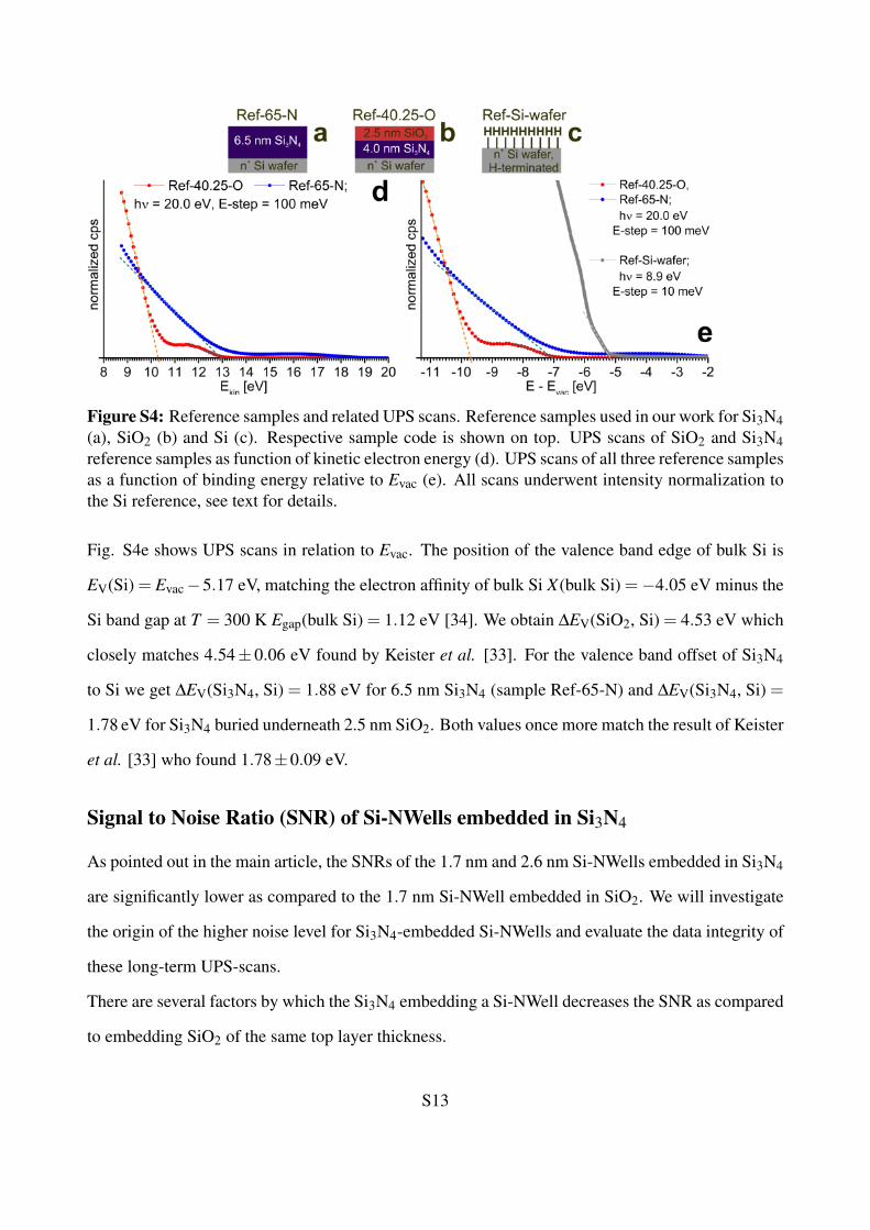
Figure S4: Reference samples and related UPS scans. Reference samples used in our work for Si3N4(a), SiO2 (b) and Si (c). Respective sample code is shown on top. UPS scans of SiO2 and Si3N4reference samples as function of kinetic electron energy (d). UPS scans of all three reference samplesas a function of binding energy relative to Evac (e). All scans underwent intensity normalization tothe Si reference, see text for details.
Fig. S4e shows UPS scans in relation to Evac. The position of the valence band edge of bulk Si is
EV(Si) = Evac−5.17 eV, matching the electron affinity of bulk Si X(bulk Si) =−4.05 eV minus the
Si band gap at T = 300 K Egap(bulk Si) = 1.12 eV [34]. We obtain ∆EV(SiO2, Si) = 4.53 eV which
closely matches 4.54± 0.06 eV found by Keister et al. [33]. For the valence band offset of Si3N4
to Si we get ∆EV(Si3N4, Si) = 1.88 eV for 6.5 nm Si3N4 (sample Ref-65-N) and ∆EV(Si3N4, Si) =
1.78 eV for Si3N4 buried underneath 2.5 nm SiO2. Both values once more match the result of Keister
et al. [33] who found 1.78±0.09 eV.
Signal to Noise Ratio (SNR) of Si-NWells embedded in Si3N4
As pointed out in the main article, the SNRs of the 1.7 nm and 2.6 nm Si-NWells embedded in Si3N4
are significantly lower as compared to the 1.7 nm Si-NWell embedded in SiO2. We will investigate
the origin of the higher noise level for Si3N4-embedded Si-NWells and evaluate the data integrity of
these long-term UPS-scans.
There are several factors by which the Si3N4 embedding a Si-NWell decreases the SNR as compared
to embedding SiO2 of the same top layer thickness.
S13

The ratio of packing fractions of α-Si3N4 to SiO2 (Cristobalite) is P(Si3N4/SiO2) = 1.36
[31], whereby Si3N4 provides 36% more scattering centres per unit volume as compared to
SiO2. This finding is reflected in the normalized cps of the 1.7 nm NWell samples (Fig. 4b
in main article): The valence HOS of the Si-NWell in Si3N4 has a normalized cps at ca.
1/P(Si3N4/SiO2) = 1/1.36 = 74% of the cps range where the valence HOS occurs for the
Si-NWell embedded in SiO2. In other words, the 1.5 nm Si3N4 top layer is effectively as thick as a
2.0 nm SiO2 layer as far as inelastic electron scattering is concerned. We can verify this statement
for the two 1.7 nm Si-NWells when looking at the normalized signal at the cps ranges of the valence
HOS of the respective NWell, yielding 692±70 cps for sample QW-17-N (954±206 cps for sample
QW-17-O). From these values we obtain a cps ratio of 692±70/954±206≈ 0.72 which alignes to
1/P(Si3N4/SiO2) = 0.74. The difference in packing fraction is not the only effect to decrease the
SNR, though.
It is well known that Si3N4 has significantly higher electronic defect densities within its fundamental
gap as compared to SiO2. Indeed, such defects (Urbach tails [34]) can be seen in Fig. 4b of the
main article, where the tail states for samples Si-26-N and in particular Si-17-N become much
more prominent as compared to sample Si-17-O. The effect of quantum confinement on the SNR is
evident from the cps range of the Si-NWell valence HOS of sample QW-26-N which shows a higher
SNR at a lower intensity of 615± 98 cps although the NWell is 1.5 times thicker than in sample
QW-17-N. Lower quantum confinement of sample QW-26-N shifts its valence HOS further away
from the valence band edge of Si3N4 and its Urbach tail, resulting in a decreased electronic DOS
associated with Si3N4 at the energy range where the NWell valence HOS occurs, thereby increasing
its SNR.
In addition to higher defect densities within the entire fundamental gap, the energy of the valence
band edge of Si3N4 with Evac− 7.05 eV is much nearer to the valence HOS of Si-NWells as com-
pared to SiO2 (Evac−9.70 eV, see section ). Thereby, the Si3N4 valence band DOS and associated
Urbach tails provide a yet higher background to the valence HOS signal of the Si-NWells, masking
the valence HOS signal of the Si-NWells. The electron affinity X of Si3N4 is ca. −1.6 eV, about
S14
twice as low as the value for SiO2 (−0.8 eV), giving way to a wider energy range of Si3N4 where
inelastic electron scattering occurs. This contribution further diminishes the cps of excited primary
(unperturbed) electrons originating from the valence HOS of the Si-NWell in Si3N4.
Another feature contributing to energetic blurring of the valence HOS of Si3N4-embedded Si-
NWells is their poly-Si nature. Such NWells were processed by depositing and annealing ultrathin
amorphous (a-) Si layers, with Si3N4 known to restrict a-Si crystallisation as compared to SiO2
due to its higher Young’s modulus and associated strain [35]. Resulting poly-Si NWells have
multiple interface orientations and wider deviations in NWell thickness. Although the ICT is far
from saturating at ultrathin NWells [22], it induces a minor energetic shift of the valence HOS as
a function of interface orientation [30]. Thickness deviations of NWells add to signal blurring as
they change the ratio of Si (NWell) atoms per interface bond. This ratio is a key parameter of the
ICT impact which induces the energetic shift of the electronic structure of usn-Si [30]. Although
the minor thickness deviations encountered here will not induce a major electronic shift, they will
suffice to blurr the energetic position of the valence HOS of NWells in the range of a couple of
10 meV. Another obvious reason for signal blurring is the change in quantum confinement with
NWell thickness in particuler for the 1.7 nm NWell.
Unfortunately, a further-going quantitative analysis of these phenomena on the SNR of the Si-
NWells embedded in Si3N4 is not possible nor worthwhile as the exact spot used in UPS would have
to be characterized by several other techniques, some of which are destructive to the sample. The
solution is to resort to SOI sample processing with Si3N4-embedding in analogy to the SOI sample
QW-17-O featuring a SiO2-embedded 1.7 nm Si-NWell consisting of c-Si with {001} interface
orientation. Sucessfully processing such Si-NWells in Si3N4 is vastly more complex as compared to
SiO2-based SOI processing and a current focus of technological development.
We now turn to the data integrity of the Si3N4-embedded samples QW-17-N and QW-26-N. For the
c-Si NWell in SiO2 (sample QW-17-O), we see a clear feature of a valence HOS (see Fig. 4b in
main article); this sample is therefore not considered here.
S15
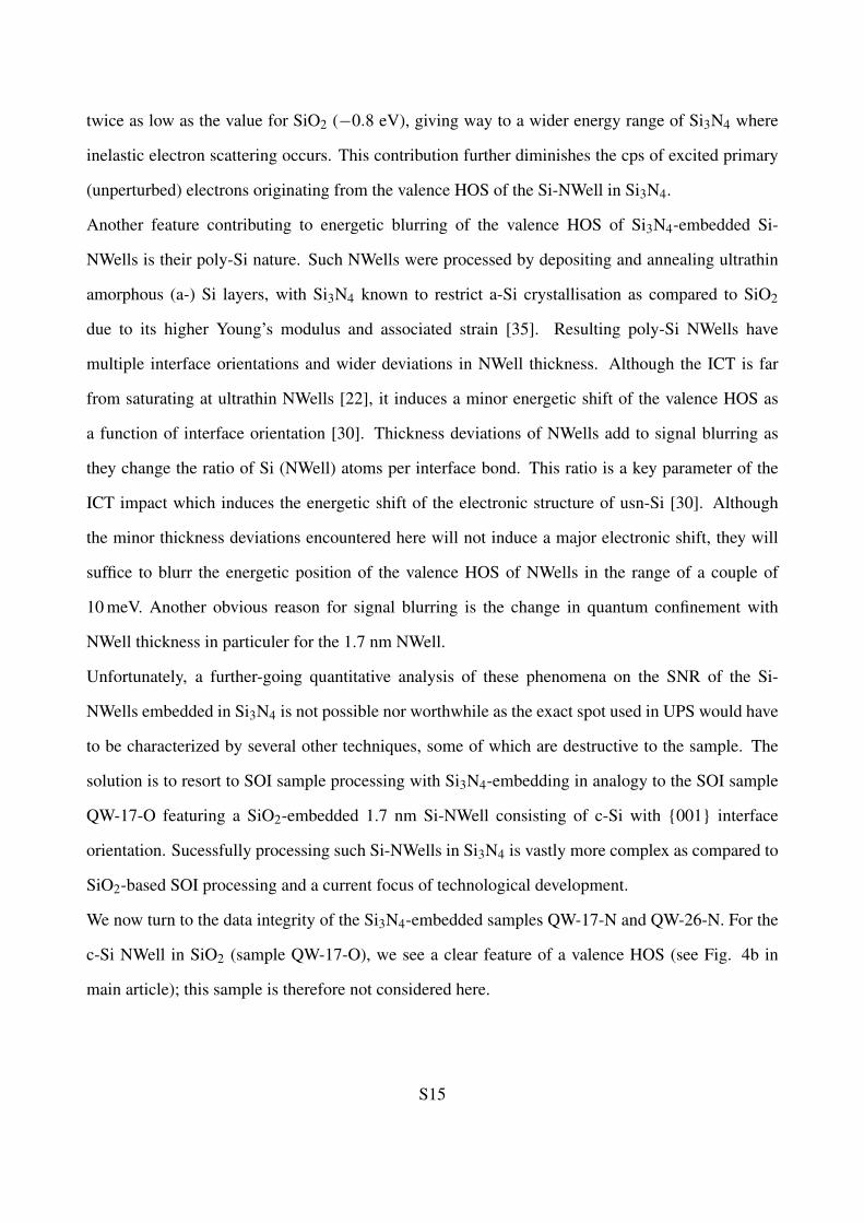
Figure S5: Difference between full UPS signal and fit to amorphous background due to Si3N4-embedding of Si-NWells as shown in Fig. 4b of main article for sample QW-17-N having a Si-NWellthickness of 1.7 nm (a) and for sample QW-26-N having a Si-NWell thickness of 2.6 nm (b). Cyan(light green) lines show local linear fits to the signal difference excluding the signal originating fromthe 1.7 nm (2.6 nm) Si-NWell. Data points assigned to the Si-NWells are shown as spheres. Formore details see text.
The valence HOS feature of both Si-NWells embedded in Si3N4 are fairly weak as compared to
the respective feature of sample Si-17-O. We therefore plot the difference between the UPS signal
(normalized cps) to the fit of the amorphous background describing the electronic DOS of Si3N4
in the vicinity of the valence HOS feature of the respective NWell, see Fig. 4b in main article. In
addition, we apply a linear fit to each region of the difference signal above and below the energy
range of the valence HOS assigned to the respective Si-NWell. These data are plotted for the 1.7 nm
NWell in Fig. S5a and for the 2.6 nm NWell in Fig. S5b.
We first consider sample QW-26-N which shows a clear feature above the two linear fits of the
differential signal. This feature can be assigned to the presence of the 2.6 nm NWell straight away
as it clearly stands out above the local a-Si3N4 background. The feature of the 1.7 nm NWell is
just visible above the a-Si3N4 background. It contains 10 data points, while fluctuations of the same
magnitude due to noise in adjacent energy ranges contains only up to 4 data points above the linear
fit. It appears that 1.7 nm is the minimum thickness of a poly-Si NWell in Si3N4 to still get detected
by long-term UPS of at least 12 h to maximize the SNR of UPS scans. Such valence HOS features
could be significantly enhanced if the NWell consisted of c-Si with defined interface orientation
embedded in high-quality thermal Si3N4, see above.
S16
Derivation of Charge Carrier Densities for Non-Equilibrium Green’s
Function (NEGF) Transport Simulation of Undoped Si-Nanowire MIS-
FET Devices
As mentioned in section , real-space DFT calculations do not provide results with an absolute energy
gauge such as the vacuum energy Evac whereby we can only use relative changes in energy such as
energy offsets within one or between several approximants calculated with exactly the same DFT
computation route. We use results from UPS measurements to obtain absolute energies with respect
to Evac and apply fundamental NWire gaps and energy offsets in HOMOs ∆EHOMO obtained from
DFT calculations of the NWire approximant (Fig. 5a–c in main publication). The UPS of a 1.7 nm
Si-NWell embedded in Si3N4 yielded an energy of the HOS of EV(Si-NWire) = Evac− 5.20 eV
which yields EV(Si-NWire)=EV(bulk-Si)−0.03 eV. As drain and source electrode materials we use
Ni which is known to have an electron work function of EWF(Ni) = 5.15 eV [36] which is equivalent
to EWF(Ni) = EV(bulk-Si)+ 0.02 eV. Above values yield to EWF(Ni)−EV(Si-NWire) = 0.05 eV.
This energy difference serves to calculate the Fermi-Dirac occupation probability of the Si-NWire
valence states with holes:
fFD =1
1+ exp(
EWF(Ni)−EV(Si-NWire)kBT
) (S2)
= 0.1263 ,
with kBT presenting the thermal energy at T = 300 K. This fFD value applies to all 121 Si atoms
within the NH2-covered NWire section of the Si233(NH2)87(OH)81 approximant; NSi(NH2-term) =
121. In other words, we get one hole for every NSi(NH2-term)/ fFD = 958 atoms. Relating this
ionization probability to the atomic volume density of Si, NSi = 5.16×10²² atoms/cm−3, we arrive
at a hole density within the Si3N4-covered NWire section of p=NSi× fFD/NSi(NH2-term)= 5.36×
1019 cm−3.
The hole density on the OH-terminated section of the Si233(NH2)87(OH)81 approximant follows
S17
the reasoning outlined above with two different parameters: NSi(OH-term) = 112 and EWF(Ni)−
EV(Si-NWire) = 1.12 eV, yielding to fFD = 1.532× 10⁻¹⁹ and p = 71 cm−3. In contrast to what
this very low value suggests, it is quite stable since it reflects the energy offset between Si3N4- and
SiO2-covered Si-NWire sections. This value of p is fairly robust against carrier diffusion processes
due to the dominance of O onto the channel volume of the Si-NWire (Fig. 5a in main publication).
It can be controlled by applying a gate-source voltage counter-acting the ICT from the NWire to the
O atoms within SiO2.
Experimental input on Si-NWires with diameters of 1.7 nm as used in NEGF-Simulations from UPS-
scans would provide the ideal energy calibration for the energetic consideration above. However,
the sample volume would be too small to get useable results. With the ratio of quantum numbers
to thickness of NWires vs. NWells, we could get a good estimate of the NWire HOSs relative to
Evac. The prospective Si-NWell would need a thickness of 1/√
2 of the Si-NWire diameter due to the
ground state of the system having one quantum number for a QWell 〈1〉 and two quantum numbers
〈1|1〉 for a QWire [37]. This would mean we had to measure a Si-NWell of 1.7 nm×1/√
2 = 1.2 nm
thickness which is not feasible due to the NWell HOS signal being buried by noise, see section
. In other words, the UPS data obtained from the 1.7 nm Si-NWell embedded in Si3N4 currently
provides us with the best practicable experimental input to a 1.7 nm Si-NWire, with the prospect to
characterize yet thinner Si-NWells if SOI-processed Si3N4-based samples are at hand.
For the simulations of FET devices based on ultrathin Si-NWires with appropriate SiO2 and Si3N4
coatings to realize ICT we solved self-consistently Poisson’s and Schrödinger’s equation using the
NEGF formalism. For minimizing computational cost, a one-dimensional finite difference, effective
mass model for the electrostatics and for the NEGF is employed which has proven to provide ade-
quate results for devices based on NWires with ultrathin diameters [39,41]. As has been shown in
[42], the electrostatics of a nanowire transistors can be described well by a modified 1D equation of
the following form:
d2Φf
dx2 −Φf−Φg +Φbi
λ 2 =e(ρ(x)±N)
ε0εSi(S3)
S18

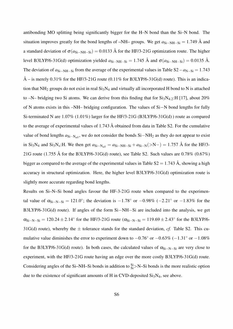
1 2 3
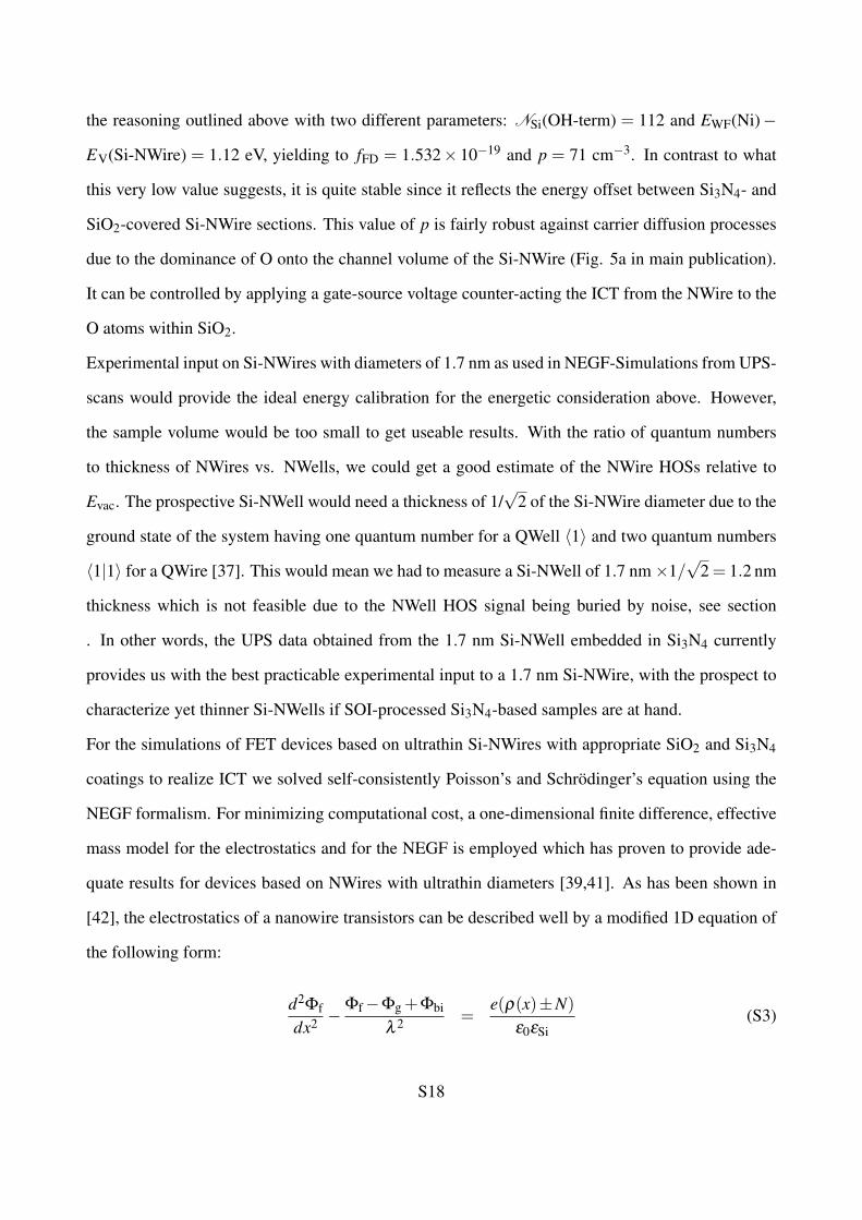
a b
gateddielec
conl
1
2
3
a
b
dnw
L
E f
3
E f
N-1
E f
2 E f
s
E f
d
r
jΣ a
.........
drain source
0.0
0.2
0.4
0.6
en
erg
y (e
V)
Si N3 4 SiO2Ni Ni
r
sΣ
r
dΣ
Figure S6: Schematics of the nanowire device under consideration. A nanowire of diameter dnw issurrounded by Si3N4 within the gate area and covered by SiO2 in the gate underlap region (lengthlcon). The nanowire is contacted with nickel contacts; fringing fields are taken into consideration withconformal mapping [38,39]. The lower panel shows the valence band through the device (solid darkgray line) and the spatial dependence of the quasi-Fermi level (red dashed line). Buettiker probes(red contacts) are attached at each finite difference grid size [40]; the Buettiker probes are isolatedvirtual contacts whose (quasi-)Fermi level is found self-consistently based on the requirement thateach Buettiker probe carries zero net current.
where Φf, Φg and Φbi are the surface potential, the gate potential and the built-in potential, respec-
tively, and ρ(x) is the density of free carriers. The length λ represents a screening length for potential
variations and its functional form depends on the system under consideration. In the present case
of a gate-all-around nanowire FET we approximate the actual cylindrical device layout with a ge-
ometry consisting of four gates placed around the nanowire and hence λ =√
εSiεSi3N4
dchddielec/4 [39].
Within the un-gated underlap region of length lcon, fringing fields of the gate need to be taken into
consideration. To this end, the area bounded by the points 1,2,3 and a, b in cartesian coordinates
is conformally mapped onto a parallel plate capacitor (see Fig. S6) [38]. On transforming back
the electric field lines, a spatially dependent ddielec(x) and hence λ (x) =√
εSi4εair
ddielec(x)dnw are ob-
tained that allow using Eqn. (S3) for the entire device; note that for simplicity we neglected the small
contribution of the SiO2-layer to the effective dielectric constant within the gate underlap region.
The charge in and current through the device is computed self-consistently assuming one-
dimensional electronic transport through the nanowire as appropriate for the dimensions of the
S19
nanowire considered here. An effective mass approximation is used for the conduction and valence
band and the complex band structure within the band gap is taken into consideration via Flietner’s
dispersion relation [43]. The magnitude of the band gap is take from the h-DFT calculations (see
above). In order to describe inelastic carrier scattering, Buettiker probes are attached to each finite
difference site (illustrated with the circles in Fig. S6) as displayed in the lower panel of Fig. S6. A
mean free path of lmfp = 5 nm has been assumed giving rise to the quasi-Fermi level distribution
shown in Fig. S6 (red dashed line).
References
1. J. S. Binkley, J. A. Pople, W. J. Hehre, J. Am. Chem. Soc. 1980, 102, 939.
2. K. D. Dobbs, W. J. Hehre, J. Comp. Chem. 1987, 8, 880.
3. J. B. Foresman, A. Frisch, Exploring Chemistry with Electronic Structure Methods (2. Ed.),
Gaussian Inc., Wallingford, CT, USA (1998).
4. D. König, J. Rudd, G. Conibeer, M. A. Green, Phys. Rev. B 2008, 78, 035339.
5. EPAPS document to [4].
6. C. B. R. dos Santos, C. C. Lobato, J. B. Vieira, D. S. B. Brasil, A. U. Brito, W. J. C. Macêdo,
J. C. T. Carvalho, J. C. Pinheiro, Comp. Molec. Biosci. 2013, 3, 66.
7. S. Kümmel, L. Kronik, Rev. Mod. Phys. 2008, 80, 3.
8. 2008 ARC Photovoltaics Centre of Excellence Annual Report, 2008, p. 86 hardcopy [p. 88 pdf
file].
9. D. König, S. Gutsch, H. Gnaser, M. Wahl, M. Kopnarski, J. Göttlicher, R. Steininger, M.
Zacharias, D. Hiller, Sci. Rep. 2015, 5, 09702.
S20
10. D. König, The Introduction of Majority Carriers into Group IV Nanocrystals (Chapter 7), pp.
203-254, in Valenta, J., Mirabella, S. (Eds.) Nanotechnology and Photovoltaic Devices, Pan
Stanford Publishing, Singapore (2015).
11. D. König, J. Rudd, G. Conibeer, M. A. Green, Mat. Sci. Eng. B 2009, 159-160, 117.
12. R. L. Mozzi, B. E. Warren, J. Appl. Cryst. 1969, 2, 164.
13. J. R. G. Da Silva, D. G. Pinatti, C. E. Anderson, M. L. Rudee, Phil. Mag. 1975, 31, 713.
14. L. W. Hobbs, C. E Jesurum, B. Berger, The Topology of Silica Networks (Chapter 1), pp. 3-47,
in R. A. B. Devine, J.-P. Durand, E. Dooryhée (Eds.) Structure and Imperfections in Amorphous
and Crystalline Silicon Dioxide, Wiley & Sons, Chichester (2000).
15. R. Hezel, C. Jaeger, J. Electrochem. Soc. 1989, 136, 518.
16. L. Cai, A. Rohatgi, S. Han, G. May, M. Zou, J. Appl. Phys. 1989, 83, 5885.
17. A. Iqbal, W. B. Kackson, C. C. Tsai, J. W. Allen, C. W. Bates Jr., J. Appl. Phys. 1987, 61, 2947.
18. T. Aiyama, T. Fukuyama, K. Niihara, T. Hirai, K. Suzuki, J. Non-Cryst. Sol. 1979, 33, 131.
19. M. Misawa, T. Fukunaga, K. Niihara, T. Hirai, K. Suzuki, J. Non-Cryst. Sol. 1979, 34, 313.
20. S. Hasegawa, L. He, Y. Amano, T. Inokuma, Phys. Rev. B 1993, 48, 5315.
21. F. Rissner, D. A. Egger, A. Natan, T. Körzdörfer, S. Kümmel, L. Kronik, E. Zojer, J. Am. Chem.
Soc. 2011, 133, 18634.
22. D. König, D. Hiller, S. Gutsch, M. Zacharias, Adv. Mater. Interfaces 2014, 1, 1400359.
23. R. W. Hunter, S. A. Malo, J. Phys. Chem. Sol. 1969, 30, 2739.
24. D. A. Stephenson, N. J. Binkowski, J. Non-Cryst. Sol. 1976, 22, 399.
25. R. J. Powell, G. F. Derbenwick, IEEE Tr. Nucl. Sci. 1971, 18, 99.
S21
26. D. H. DiStefano, D. E. Eastman, Sol. Stat. Comm. 1971, 9, 2259.
27. H. Ibach, J. E. Rowe, Phys. Rev. B 1974, 10, 710.
28. R. J. Powell, M. Morad, J. Appl. Phys. 1978, 49, 2499.
29. H. Kurata, H. Masataka, Y. Osaka, Jap. J. Appl. Phys. 1981, 20, L811.
30. D. König, AIP Adv. 2016, 6, 085306.
31. A. F. Holleman, E. Wiberg, N. Wiberg, Lehrbuch der Anorganischen Chemie (101. Ed.); Walter
deGruyter: Berlin, 1995; (in German).
32. S. Suga, A. Sekiyama, Photoelectron Spectroscopy – Bulk and Surface Electronic Structures,
Springer Series in Optical Sciences, Vol. 176, Springer Press, Heidelberg, 2014.
33. J. W. Keister, J. E. Rowe, J. J. Kolodziej, H. Niimi, T. E. Madey, G. Lucovsky, J. Vac. Sci. Tech.
B 1999, 17, 1831.
34. K. W. Böer, Survey of Semiconductor Physics, Vol. 1. (Van Nostrand Reinhold, New York,
1990).
35. S. R. Elliot, The Physics and Chemistry of Solids. (Wiley, Chichester, 1998).
36. S. Hala, T. Durakiewicz, J. Phys.: Cond. Matter 1998, 10, 10815.
37. J. Singh, Quantum Mechanics – Fundamentals and Applications to Technology, Wiley & Sons
(New York, 1997).
38. S. Xiong, T.-J. King, J. Bokor, Semicond. Sci. Technol. 2005, 20, 652.
39. J. Knoch, J. Appenzeller, IEEE Electron. Dev. Lett. 2010, 31, 305.
40. R. Venugopal, M. Paullson, S. Goasguen, S. Datta, M. S. Lundstrom, J. Appl. Phys. 2003, 93,
5613.
S22
41. J. Appenzeller, J. Knoch, M. T. Björk, H. Schmid, H. Riel, W. Riess, IEEE Tr. Electron. Dev.
2008, 55, 2827.
42. C. P. Auth, J. D. Plummer, IEEE Electron. Dev. Lett. 1997, 18, 74.
43. H. Flietner, Phys. Stat. Sol. 1972, 54, 201.
S23