Embed Size (px)
Citation preview
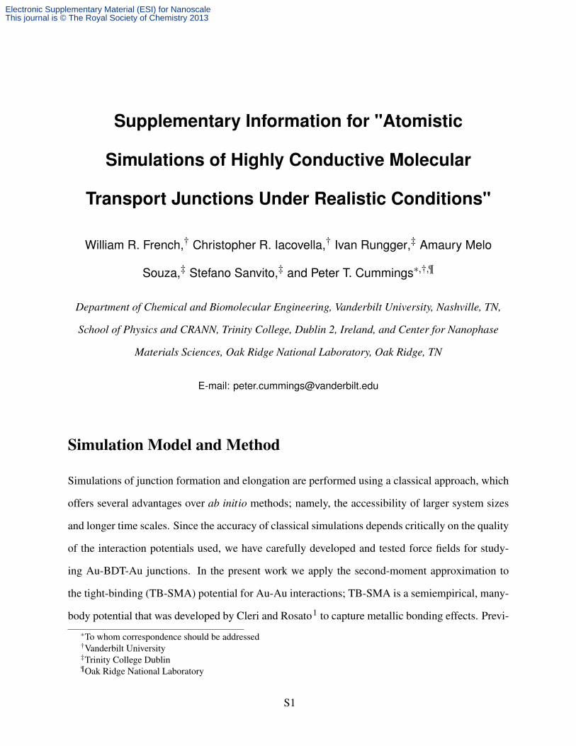
Supplementary Information for "Atomistic
Simulations of Highly Conductive Molecular
Transport Junctions Under Realistic Conditions"
William R. French,† Christopher R. Iacovella,† Ivan Rungger,‡ Amaury Melo
Souza,‡ Stefano Sanvito,‡ and Peter T. Cummings∗,†,¶
Department of Chemical and Biomolecular Engineering, Vanderbilt University, Nashville, TN,
School of Physics and CRANN, Trinity College, Dublin 2, Ireland, and Center for Nanophase
Materials Sciences, Oak Ridge National Laboratory, Oak Ridge, TN
E-mail: [email protected]
Simulation Model and Method
Simulations of junction formation and elongation are performed using a classical approach, which
offers several advantages over ab initio methods; namely, the accessibility of larger system sizes
and longer time scales. Since the accuracy of classical simulations depends critically on the quality
of the interaction potentials used, we have carefully developed and tested force fields for study-
ing Au-BDT-Au junctions. In the present work we apply the second-moment approximation to
the tight-binding (TB-SMA) potential for Au-Au interactions; TB-SMA is a semiempirical, many-
body potential that was developed by Cleri and Rosato1 to capture metallic bonding effects. Previ-
∗To whom correspondence should be addressed†Vanderbilt University‡Trinity College Dublin¶Oak Ridge National Laboratory
S1
Electronic Supplementary Material (ESI) for NanoscaleThis journal is © The Royal Society of Chemistry 2013
ously,2 we tested three widely used Au-Au many-body potentials, finding that TB-SMA provided
the closest match to density functional theory (DFT) for describing the energetic and structural
evolution of elongating Au nanowires. We have also shown that elongating nanowires modeled
with TB-SMA yield conductance behavior similar to that of wires stretched with a highly accurate
reactive potential.3 For S-Au interactions, which exhibit complex bonding characterized by multi-
ple stable bonding sites, we employ Morse potential curves for BDT bonding at the on-bridge and
on-top sites; on-bridge sites are energetically favored for BDT,4 while on-top sites are important
in low-coordination environments (e.g., bonding to an atomically sharp tip).5 The curves were cal-
ibrated against DFT calculations, with three functionals tested for exchange and correlation.6 The
remaining interactions, including BDT intramolecular interactions, nonbonded interactions be-
tween BDT molecules and BDT and Au, and electrostatic interactions arising from partial charges
residing on the atoms belonging to BDT, are described elsewhere.7 We have confirmed that our
interaction models provide conductance results consistent with structures optimized with DFT, see
the Benchmark Calculations section below.
In the hybrid molecular dynamics-Monte Carlo (MD-MC) simulations, we begin with a small
Au nanowire (eight atoms long and three atoms thick) connected between two rigid [100]-oriented
leads (four atoms long and six atoms thick), we obtain a monolayer of BDT (consisting of 30-
36 chemisorbed molecules) on the junction by performing MC moves in the semigrand canonical
ensemble; a mixture of BDT molecules capable of bonding at on-top and on-bridge sites are sim-
ulated, with molecule identity swap moves incorporated to sample the preferred BDT bonding
geometries. The non-adsorbed BDT are next removed from the simulation box and 20 million
constant-NV T (where N is the number of BDT molecules, V is the volume, and T is the temper-
ature) moves are performed to equilibrate the monolayer. Stretching of the BDT-coated wire is
carried out by displacing the right-side lead layers in 0.1 Å intervals in the [100] direction, with
20 ps of MD and 100,000 MC moves at constant NV T applied between intervals. The stretching
procedure is repeated until the rupture of the Au nanowire occurs, at which point individual BDT
molecules may chemically attach between the ruptured tips. In runs where a molecular junction
S2
Electronic Supplementary Material (ESI) for NanoscaleThis journal is © The Royal Society of Chemistry 2013
forms, we continue elongating the junction to the point of rupture. For simplicity, we remove all
remaining BDT molecules from the simulation once a molecular junction forms, so that we may
focus on electrode structure effects. During the Au-BDT-Au stretching process, geometries are
periodically (every ∼0.5-1.0 Å of elongation and immediately prior to rupture) extracted for use
in conductance calculations.
The MD simulations are performed in LAMMPS,8 extended to include the TB-SMA potential.
The velocity Verlet algorithm in combination with the rRESPA multiple time scale integrator is
used to integrate the equations of motion, with outer and inner loop timesteps of 2.0 fs and 0.4
fs, respectively. We apply the Nosé-Hoover thermostat to control the temperature at 77 K. This
temperature is chosen because TB-SMA performs better at low temperature,3 and also because 77
K is commonly used in experiments.9 The MC moves are performed using an in-house code, and
are incorporated to ensure sufficient sampling of the metal-molecule bonding geometries and to
overcome time scale limitations.
Conductance Calculation Details
Elongation Simulations and Benchmark Geometries
For the conductance calculations, we utilize the DFT code SIESTA10 to self-consistently solve
for the electronic structure, followed by the Green’s functions approach as implemented in the
SMEAGOL11,12 package to calculate the zero-bias conductance, given by G = T (εF)G0, where T
is the transmission probability, εF is the electrode Fermi level, and G0=2e2
h . Norm-conserving pseu-
dopotentials and a double-ζ with polarization function (DZP) numerical atomic orbital basis set are
used for all atoms. For the exchange and correlation functional, we employ an approximate self-
interaction correction (ASIC)13 method to the local density approximation (LDA), which yields
improved values of the conductance through Au-BDT-Au junctions by more accurately predicting
the energy level lineup between the molecule and two leads.14,15 ASICs are used for all non-metal
atoms, where self-interaction errors are most prominent. Note that whereas for isolated molecules
S3
Electronic Supplementary Material (ESI) for NanoscaleThis journal is © The Royal Society of Chemistry 2013
applying the full ASIC usually gives good agreement with experimental values for ionization po-
tentials (IPs), in general the IP decreases as the molecule is brought closer to a metallic electrode
due to image charge formation in the metal.16 To take into account this metal induced reduction
of the IP, we use a scaling parameter equal to 0.5 for the amount of ASIC that is added.13 We
apply a confining energy shift of 0.03 eV, and a cutoff of 600 Ry for the grid integration. A 3 x
3 Monkhorst-Pack k-point sampling of the surface Brillouin zone is employed for calculating the
electron density and transmission (except for the benchmark calculations, see below). We have
carefully tested and verified that this k-point sampling scheme provides good convergence of the
transmission with six layers of Au lead atoms on both sides of the junction.
Conductance Histograms
0 2 4 6 8
Elongation Length (Å)
0
0.05
0.1
0.15
0.2
0.25
G (
2e2 / h
) spd-Au Leadss-Au Leads
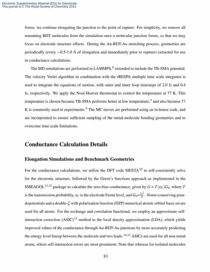
Figure S1: Calculated conductance trace using the DZP 5d6s6p and SZ 6s-only basis set for thelead atoms.
To reduce the computational cost of the conductance histogram calculations, we employ a 6s-
only single-ζ basis set for the lead atoms14 (the full basis set is still applied for all other atoms).
The zero-bias conductance and transmission resulting from application of a reduced basis set com-
pare well with results obtained using the full basis set. Figure S1 compares the conductance for
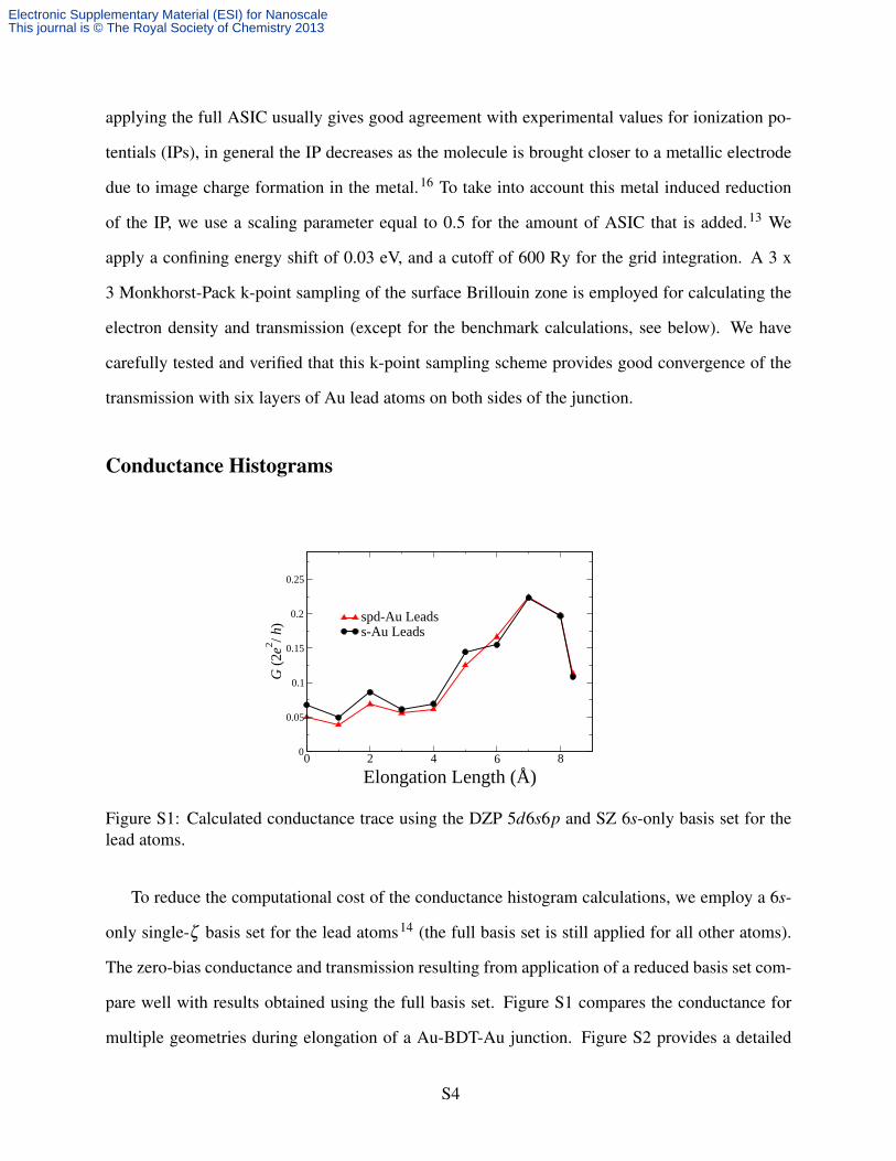
multiple geometries during elongation of a Au-BDT-Au junction. Figure S2 provides a detailed
S4
Electronic Supplementary Material (ESI) for NanoscaleThis journal is © The Royal Society of Chemistry 2013
0 10 20 30 40 50Z (Å)
-20
-15
-10
-5
0
Har
tree
Pot
entia
l (eV
)
spd-Au Leadss-Au Leads
-4 -2 0 2 4ε - εF (eV)
0
0.2
0.4
0.6
0.8
1
T
spd-Au Leads (0.166)s-Au Leads (0.155)
Figure S2: Detailed comparison for the reduced and full basis sets. Calculated Hartree potential(top) and transmission (bottom) using the DZP 5d6s6p and SZ 6s-only basis set for the lead atoms.The zero-bias conductance is shown in parentheses.
comparison for a single geometry at elongation length = 6 Å in Figure S1. While there is less
charge present in the leads for the simplified basis set, the features in the transmission, especially
around εF , are still adequately captured.
S5
Electronic Supplementary Material (ESI) for NanoscaleThis journal is © The Royal Society of Chemistry 2013
Benchmark Calculations
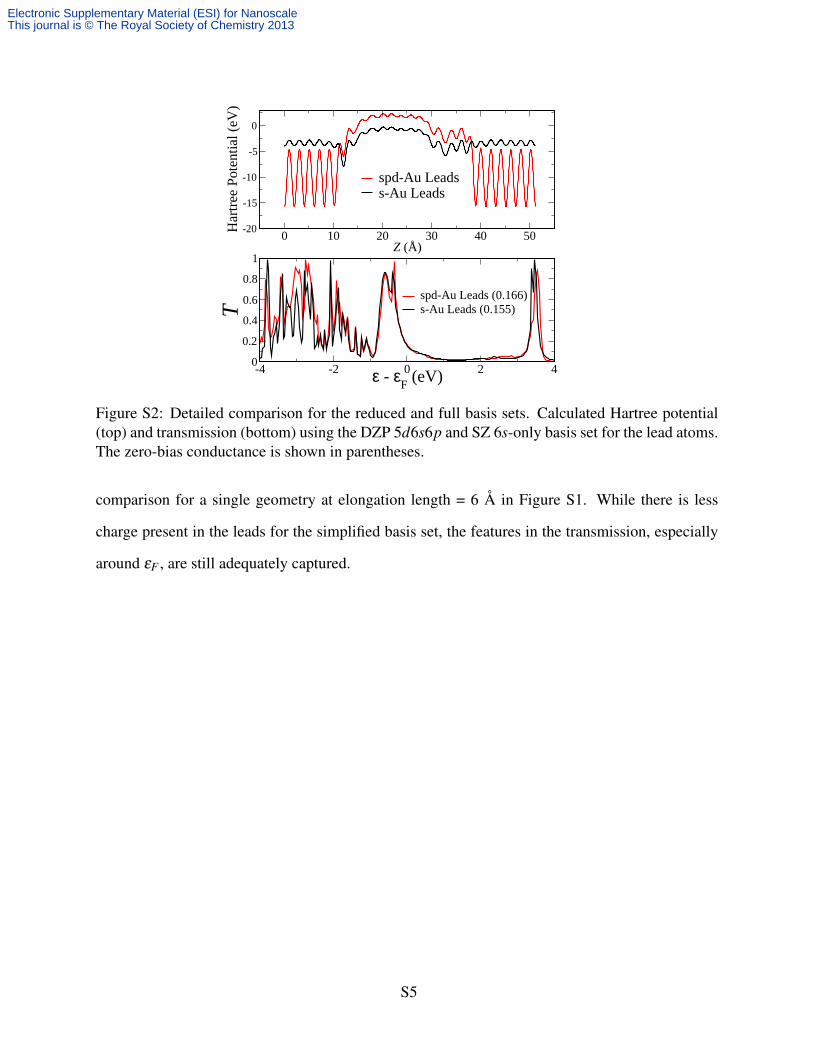
Figure S3: Benchmark geometries.
Table S1: Results for benchmark calculations.
(100) Surfaces (111) Surfaces (100) Tips (111) Tips
G (2e2
h ) 0.060 0.061 0.083 0.143
εHOMO − εF (eV) -1.708 -1.548 -1.427 -1.106
T (εHOMO) 0.825 1.004 1.365 1.695
To access the accuracy of the interaction potentials, we calculate the conductance of four
benchmark systems for comparison to results in literature, with the geometry of each system first
optimized by using the interaction potentials. Each system contains a single BDT molecule sand-
wiched between two Au electrodes. The electrodes tested are: (100) surfaces, (111) surfaces, (100)
tips, and (111) tips, as shown in Figure S3. Each lead consists of six layers, with Au(100) and
Au(111) containing eight and twelve atoms per layer, respectively. We apply a 3 x 3 Monkhorst-
Pack k-point sampling of the surface Brillouin zone for calculating the electron density and 6 x
6 k-point sampling for calculating transmission (except the (111) tips, where we use 12 x 12 k-
point sampling for calculating the transmission). The geometry of each system is optimized by
applying the previously described interaction potentials to the following “quench” MD minimiza-
tion protocol. After positioning each S atom at the on-bridge (for surfaces) or on-top (for tips)
site of each electrode, we relax the BDT geometry and electrode-electrode distance by applying
the Nosé-Hoover thermostat at 0.01 K and treating each electrode as a rigid body free to move in
S6
Electronic Supplementary Material (ESI) for NanoscaleThis journal is © The Royal Society of Chemistry 2013
the axial direction; the BDT and Au atoms in the first two layers (and tips, if applicable) of each
surface are then allowed to relax at 0.01 K.
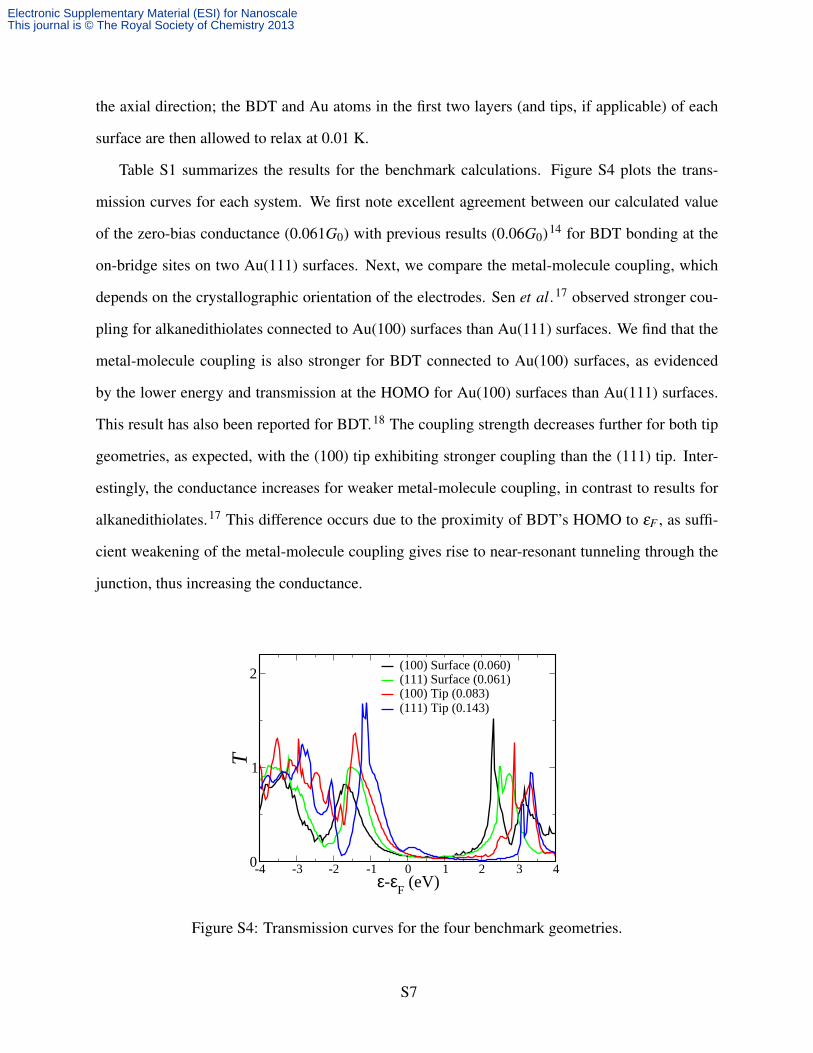
Table S1 summarizes the results for the benchmark calculations. Figure S4 plots the trans-
mission curves for each system. We first note excellent agreement between our calculated value
of the zero-bias conductance (0.061G0) with previous results (0.06G0)14 for BDT bonding at the
on-bridge sites on two Au(111) surfaces. Next, we compare the metal-molecule coupling, which
depends on the crystallographic orientation of the electrodes. Sen et al.17 observed stronger cou-
pling for alkanedithiolates connected to Au(100) surfaces than Au(111) surfaces. We find that the
metal-molecule coupling is also stronger for BDT connected to Au(100) surfaces, as evidenced
by the lower energy and transmission at the HOMO for Au(100) surfaces than Au(111) surfaces.
This result has also been reported for BDT.18 The coupling strength decreases further for both tip
geometries, as expected, with the (100) tip exhibiting stronger coupling than the (111) tip. Inter-
estingly, the conductance increases for weaker metal-molecule coupling, in contrast to results for
alkanedithiolates.17 This difference occurs due to the proximity of BDT’s HOMO to εF , as suffi-
cient weakening of the metal-molecule coupling gives rise to near-resonant tunneling through the
junction, thus increasing the conductance.
-4 -3 -2 -1 0 1 2 3 4ε-ε
F (eV)
0
1
2
T
(100) Surface (0.060)(111) Surface (0.061)(100) Tip (0.083)(111) Tip (0.143)
Figure S4: Transmission curves for the four benchmark geometries.
S7
Electronic Supplementary Material (ESI) for NanoscaleThis journal is © The Royal Society of Chemistry 2013

Potential Energy Evolution of Elongating Junction
-605
-604
-603
-602
Pote
ntia
l Ene
rgy
(eV
)
0 2 4 6 8Elongation Length (Å)
0.03
0.06
0.09
0.12
G (
2e2 /h
)
Figure S5: Evolution of the (top) total potential energy and (bottom) conductance of an elongatingAu-BDT-Au junction.
The shifting of the highest occupied molecular orbital into alignment with εF is not necessarily
a natural consequence of the increasing total potential energy of the Au-BDT-Au junction during
elongation. In Figure S5 we plot the total potential energy and conductance of of a junction during
elongation. The energy increases throughout elongation, up to the point of rupture at an elongation
length of 6.6 Å. Note that although the potential energy increases, the conductance remains rela-
tively flat throughout elongation, demonstrating that the structure connected to the BDT molecule
is an important determinant of the conductance.
Monatomic Chain Results
Here we present the full transmission curves for the manually created MAC structures discussed in
the main article (see Figure 2k-m). The MAC Au-Au bond length is set to 2.60 Å.19 In Figure S6 a
MAC is first inserted at the left tip, then at the left and right tips. The transmission for the original
benchmark (100) tip geometry is shown for comparison. In Figure S7 we present the projected
S8
Electronic Supplementary Material (ESI) for NanoscaleThis journal is © The Royal Society of Chemistry 2013

Figure S6: The effect on transmission of adding MACs to Au(100) tips.
Figure S7: Transmission and PDOS for the junctions shown in the top (no MAC) and bottom (twoideal MACs) images of Figure S4. (a) Transmission; (b) PDOS for left S atom; (c) PDOS for sorbital of Au atom attached to the left S atom; (d) PDOS for pz orbital of Au atom attached to theleft S atom. The green dashed curves in (c) and (d) show the same PDOS, but for the MAC atomin the left electrode not directly connected to BDT.
density of states (PDOS) for the atoms and orbitals involved in the BDT-Au bond in Figure S6.
There are clear distinctions between the PDOS for a MAC electrode and a simple tip/adatom
electrode. With a MAC present, the PDOS is enhanced around εF for the S atom connected to
S9
Electronic Supplementary Material (ESI) for NanoscaleThis journal is © The Royal Society of Chemistry 2013
a MAC, and also for the Au MAC atoms. In the case of Au, the s and pz orbitals dominate the
transport and their PDOS is oscillatory compared to the relatively constant PDOS for Au atoms
in absence of a MAC. The enhanced PDOS arises from smaller band dispersion in a Au MAC
compared to bulk Au. The magnitude and shape of the enhancement depends on various factors,
mainly the length of the MAC, but also the S-Au bonding and the remaining junction structure.
Note that in our simulated junctions a MAC forms on only one side of the molecule, and thus
the transmission resembles the single-MAC junction in Figure S6 (green curve). Figure S6 shows
that higher conductance results from the formation of a MAC on both sides of a junction, however
this scenario does not occur in our simulations as the internal stress of the junction is relieved
primarily through rearrangements (and eventually rupture) in the MAC electrode. In other words,
the structure in the non-MAC electrode remains roughly unchanged following MAC formation.
S10
Electronic Supplementary Material (ESI) for NanoscaleThis journal is © The Royal Society of Chemistry 2013
References
(1) Cleri, F.; Rosato, V. Phys. Rev. B 1993, 48, 22–33.
(2) Pu, Q.; Leng, Y.; Tsetseris, L.; Park, H. S.; Pantelides, S. T.; Cummings, P. T. J. Chem. Phys.
2007, 126, 144707.
(3) Iacovella, C. R.; French, W. R.; Cook, B. G.; Kent, P. R. C.; Cummings, P. T. ACS Nano
2011, 5, 10065–10073.
(4) Pontes, R. B.; Novaes, F. D.; Fazzio, A.; da Silva, A. J. R. J. Am. Chem. Soc. 2006, 128,
8996–8997.
(5) Sergueev, N.; Tsetseris, L.; Varga, K.; Pantelides, S. Phys. Rev. B 2010, 82, 073106.
(6) Leng, Y. S.; Dyer, P. J.; Krstic, P. S.; Harrison, R. J.; Cummings, P. T. Mol. Phys. 2007, 105,
293–300.
(7) French, W. R.; Iacovella, C. R.; Cummings, P. T. ACS Nano 2012, 6, 2779–2789.
(8) Plimpton, S. J. Comp. Phys. 1995, 117, 1–19.
(9) Tsutsui, M.; Taniguchi, M.; Kawai, T. Nano Lett. 2009, 9, 2433–2439.
(10) Ordejon, P.; Artacho, E.; Soler, J. Phys. Rev. B 1996, 53, 10441–10444.
(11) Rocha, A.; Garcia-Suarez, V.; Bailey, S.; Lambert, C.; Ferrer, J.; Sanvito, S. Phys. Rev. B
2006, 73, 085414.
(12) Rungger, I.; Sanvito, S. Phys. Rev. B 2008, 78, 035407.
(13) Pemmaraju, C. D.; Archer, T.; Sanchez-Portal, D.; Sanvito, S. Phys. Rev. B 2007, 75, 045101.
(14) Toher, C.; Sanvito, S. Phys. Rev. B 2008, 77, 155402.
(15) Pontes, R. B.; Rocha, A. R.; Sanvito, S.; Fazzio, A.; Roque da Silva, A. J. ACS Nano 2011,
5, 795–804.
S11
Electronic Supplementary Material (ESI) for NanoscaleThis journal is © The Royal Society of Chemistry 2013
(16) Neaton, J. B.; Hybertsen, M. S.; Louie, S. G. Phys. Rev. Lett. 2006, 97.
(17) Sen, A.; Kaun, C.-C. ACS Nano 2010, 4, 6404–6408.
(18) Ke, S.; Baranger, H.; Yang, W. J. Chem. Phys. 2005, 122, 074704.
(19) Zarechnaya, E. Y.; Skorodumova, N. V.; Simak, S. I.; Johansson, B.; Isaev, E. I. Comp. Mat.
Sci. 2008, 43, 522–530.
S12
Electronic Supplementary Material (ESI) for NanoscaleThis journal is © The Royal Society of Chemistry 2013