Embed Size (px)
Citation preview
Supplemental Manual forPISCES2H-B
Harmonic Balance Module,Circuit Boundary Conditions, andOther Improvements
Francis Rotella, Boris Troyanovsky,Wei-Chun Lee, Zhiping Yu, andRobert Dutton
Integrated Circuits LaboratoryStanford UniversityStanford, California 94305

Copyright 1997by The Board of Trustees of Leland StanfordJunior University.
All rights reserved.
PISCES, PISCES-II, PISCES-2ET, PISCES2H-Bare registered trademarks of Stanford University.
. vii
. . .1 . . .1 . . .1
. .3 . . .3 . .3 . . .5 . . .6 . . .7
. . .9 . . .9
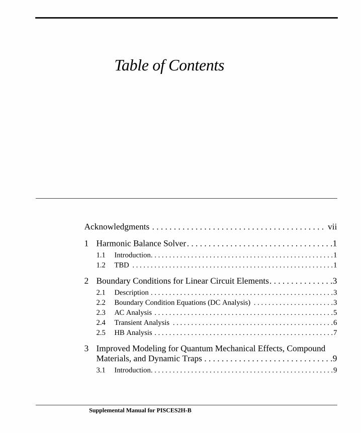
Table of Contents
Acknowledgments . . . . . . . . . . . . . . . . . . . . . . . . . . . . . . . . . . . . . . .
1 Harmonic Balance Solver. . . . . . . . . . . . . . . . . . . . . . . . . . . . . . . 1.1 Introduction. . . . . . . . . . . . . . . . . . . . . . . . . . . . . . . . . . . . . . . . . . . . . . .1.2 TBD . . . . . . . . . . . . . . . . . . . . . . . . . . . . . . . . . . . . . . . . . . . . . . . . . . . .
2 Boundary Conditions for Linear Circuit Elements. . . . . . . . . . . . .2.1 Description . . . . . . . . . . . . . . . . . . . . . . . . . . . . . . . . . . . . . . . . . . . . . . .2.2 Boundary Condition Equations (DC Analysis) . . . . . . . . . . . . . . . . . . . .2.3 AC Analysis . . . . . . . . . . . . . . . . . . . . . . . . . . . . . . . . . . . . . . . . . . . . . .2.4 Transient Analysis . . . . . . . . . . . . . . . . . . . . . . . . . . . . . . . . . . . . . . . . .2.5 HB Analysis . . . . . . . . . . . . . . . . . . . . . . . . . . . . . . . . . . . . . . . . . . . . . .
3 Improved Modeling for Quantum Mechanical Effects, CompoundMaterials, and Dynamic Traps . . . . . . . . . . . . . . . . . . . . . . . . . . . 3.1 Introduction. . . . . . . . . . . . . . . . . . . . . . . . . . . . . . . . . . . . . . . . . . . . . . .
Supplemental Manual for PISCES2H-B
Table of Contents
. . 9. . . 9
. . . 9
. 10 . . 10
. . 10
. . 10
. 10
. 11 . 11 . 11. . 11. . 12
. . 13 . 13. . 13. 14. 15 . 18. 20 . 21 . 22 . 25 . 2627
282930. 31. 32. 39
3.2 Quantum Mechanical Correction . . . . . . . . . . . . . . . . . . . . . . . . . . . . . .3.2.1 Hansch Model . . . . . . . . . . . . . . . . . . . . . . . . . . . . . . . . . . . . . . . . . . . . .
3.2.2 Van Dort Model. . . . . . . . . . . . . . . . . . . . . . . . . . . . . . . . . . . . . . . . . . . .
3.3 New Compound Materials. . . . . . . . . . . . . . . . . . . . . . . . . . . . . . . . . . . .3.3.1 SiGe Hetero-structure . . . . . . . . . . . . . . . . . . . . . . . . . . . . . . . . . . . . . . .
3.3.2 Ternary Compounds . . . . . . . . . . . . . . . . . . . . . . . . . . . . . . . . . . . . . . . .
3.3.3 Quaternary Compounds . . . . . . . . . . . . . . . . . . . . . . . . . . . . . . . . . . . . .
3.4 Dynamic Trapping Analysis . . . . . . . . . . . . . . . . . . . . . . . . . . . . . . . . . .
4 Improved Numerical Techniques for High Frequency Analysis,Newton Projections, and One Dimensional Simulations . . . . . . . .4.1 Introduction . . . . . . . . . . . . . . . . . . . . . . . . . . . . . . . . . . . . . . . . . . . . . . .4.2 High Frequency Analysis . . . . . . . . . . . . . . . . . . . . . . . . . . . . . . . . . . . .4.3 Newton Projections . . . . . . . . . . . . . . . . . . . . . . . . . . . . . . . . . . . . . . . . 4.4 One Dimensional Mode . . . . . . . . . . . . . . . . . . . . . . . . . . . . . . . . . . . .
5 Users Manual . . . . . . . . . . . . . . . . . . . . . . . . . . . . . . . . . . . . . . . .5.1 Introduction . . . . . . . . . . . . . . . . . . . . . . . . . . . . . . . . . . . . . . . . . . . . . . .5.2 PISCES Card Additions . . . . . . . . . . . . . . . . . . . . . . . . . . . . . . . . . . . .
CONTACT . . . . . . . . . . . . . . . . . . . . . . . . . . . . . . . . . . . . . . . . . . . . . . . HBMETH . . . . . . . . . . . . . . . . . . . . . . . . . . . . . . . . . . . . . . . . . . . . . . . . LOG. . . . . . . . . . . . . . . . . . . . . . . . . . . . . . . . . . . . . . . . . . . . . . . . . . . . .METHOD . . . . . . . . . . . . . . . . . . . . . . . . . . . . . . . . . . . . . . . . . . . . . . . . MODEL. . . . . . . . . . . . . . . . . . . . . . . . . . . . . . . . . . . . . . . . . . . . . . . . . .SOLVE . . . . . . . . . . . . . . . . . . . . . . . . . . . . . . . . . . . . . . . . . . . . . . . . . .TRAP. . . . . . . . . . . . . . . . . . . . . . . . . . . . . . . . . . . . . . . . . . . . . . . . . . . .
5.3 The Circuit File . . . . . . . . . . . . . . . . . . . . . . . . . . . . . . . . . . . . . . . . . . . .COMMENT LINES . . . . . . . . . . . . . . . . . . . . . . . . . . . . . . . . . . . . . . . . .NUMERICAL DEVICE . . . . . . . . . . . . . . . . . . . . . . . . . . . . . . . . . . . . . .STANDARD ELEMENTS . . . . . . . . . . . . . . . . . . . . . . . . . . . . . . . . . . . .TRANSMISSION LINE . . . . . . . . . . . . . . . . . . . . . . . . . . . . . . . . . . . . . .DEPENDENT SOURCES . . . . . . . . . . . . . . . . . . . . . . . . . . . . . . . . . . . INDEPENDENT SOURCES . . . . . . . . . . . . . . . . . . . . . . . . . . . . . . . . . OPTIONS CARD . . . . . . . . . . . . . . . . . . . . . . . . . . . . . . . . . . . . . . . . . .
iv Supplemental Manual for PISCES2H-B
Table of Contents
.42. .46. .46
. .47 . .47 . .47 . . 48
. . 48
. .48 . 48
. 48
. . 48
. .48
. . . 51
. 53
. .54 . 55
. 57
. 58
. . .63
ANALYSIS CARDS . . . . . . . . . . . . . . . . . . . . . . . . . . . . . . . . . . . . . . . . 5.4 NODE NUMBERS . . . . . . . . . . . . . . . . . . . . . . . . . . . . . . . . . . . . . . . . 5.5 SCALING FACTORS. . . . . . . . . . . . . . . . . . . . . . . . . . . . . . . . . . . . . . .
6 Examples . . . . . . . . . . . . . . . . . . . . . . . . . . . . . . . . . . . . . . . . . . .6.1 Description . . . . . . . . . . . . . . . . . . . . . . . . . . . . . . . . . . . . . . . . . . . . . . .6.2 Examples Exercising the Improved Numerics . . . . . . . . . . . . . . . . . . . .
6.2.1 Convergence in a Non-Planar Avalanche Photo Diode . . . . . . . . . . . . . .
6.2.2 High Frequency Analysis . . . . . . . . . . . . . . . . . . . . . . . . . . . . . . . . . . . .
6.3 Applications for the New Physical Models . . . . . . . . . . . . . . . . . . . . . . 6.3.1 C-V Characteristics Using van Dort QM Model . . . . . . . . . . . . . . . . . . . .
6.3.2 AC Analysis of MOSFET Using Hansch QM Model . . . . . . . . . . . . . . . .
6.3.3 Traps in a GaAs Diode. . . . . . . . . . . . . . . . . . . . . . . . . . . . . . . . . . . . . . .
6.4 Circuit Boundary Conditions . . . . . . . . . . . . . . . . . . . . . . . . . . . . . . . . . 6.4.1 Diode with External Circuit Components and Distributed Contact
Resistance48
6.4.2 Transient Response of a BJT Inverter . . . . . . . . . . . . . . . . . . . . . . . . . .
6.4.3 Gain vs. Bias Condition for a BJT Amplifier . . . . . . . . . . . . . . . . . . . . . .
6.5 Harmonic Balance Analysis . . . . . . . . . . . . . . . . . . . . . . . . . . . . . . . . . .6.5.1 Large Signal Analysis of AM Demodulator . . . . . . . . . . . . . . . . . . . . . . .
6.5.2 BJT Mixer to Down Covert a 2Mhz Signal to 100KHz . . . . . . . . . . . . . .
6.5.3 Analyzing Gain and Efficiency in a MOS Power Amplifier . . . . . . . . . . .
References . . . . . . . . . . . . . . . . . . . . . . . . . . . . . . . . . . . . . . . . . . . .
Supplemental Manual for PISCES2H-B v

Table of Contents
vi Supplemental Manual for PISCES2H-B
Acknowledgments
t and
search
The authors would like to acknowledge the following industrial partners who have provided inpu
guidance in the development of various parts of this code:
• Hewlett Packard, Santa Rosa, CAHarmonic balance solver development.
• Motorola, Tempe AZHarmonic balance simulation of RF devices.
• Matsushita Electric Industrial Co.Harmonic balance simulation of RF devices.
• Hewlett Packard, Palo Alto, CAQuantum mechanical effects in MOS devices.
The authors would like to acknowledge the continued support of the Semiconductor Re
Corporation through contract #SRC 07-SJ-116.
Supplemental Manual for PISCES2H-B vii

Acknowledgments
viii Supplemental Manual for PISCES2H-B
CHAPTER 1Harmonic Balance Solver
wlett
e the
ISCES.
r to the
ctor
1.1 Introduction
The Harmonic balance solver is an addition to PISCES provided by the EEsof Division of He
Packard. The solver is designed to interface with Stanford’s version PISCES2H-B to provid
numerical capabilities to solve the harmonic balance system of equations generated from P
This section discusses those numerics and procedures, but for a full description please refe
dissertation,Frequency Domain Algorithms for Simulating Large Signal Distortion in Semicondu
Devices, by Boris Troyanovsky.
1.2 TBD
Supplemental Manual for PISCES2H-B 1

Harmonic Balance Solver
2 Supplemental Manual for PISCES2H-B
CHAPTER 2Boundary Conditions forLinear Circuit Elements
circuit
linear
dition
rminal,
at. The
,
2.1 Description
Some simple, yet important circuits consist of only one nonlinear device and a number of linear
components surrounding the device. This chapter discusses a method of including these
components in a device simulation by reducing the surrounding circuit to a set of boundary con
equations. The basics are explained with DC analysis and are then expanded to include AC, te
and harmonic balance analyses.
2.2 Boundary Condition Equations (DC Analysis)
Most device simulators allow external resistances on a contact such that
(2.1)
whereG is the conductance,Vapp is the applied voltage,Vcon is the contact voltage, andI is the current
which is a function of the semiconductor variables for that specific node.
For a linear circuit around a device, the previous equation can be expressed in a matrix form
voltages and currents become vectors andG becomes a matrix. BothG andVapp are constants. Hence
G Vapp Vcon–( ) I Ψ n p, ,( )– 0=
Supplemental Manual for PISCES2H-B 3
Boundary Conditions for Linear Circuit Elements
ich the
circuit
evice
n that
which
s three
m lay
ng the
ff
the boundary condition on a contact is dependent on the voltages on all circuit nodes to wh
contact is connected.
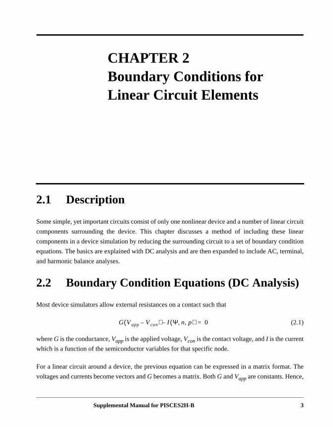
In order to determine this matrix equation, consider Figure 2.1 where we have a linear
surrounding a numerical device. Substituting ideal current sources for the numerical d
connections, modified nodal analysis (MNA) may be applied to the system with the assumptio
the device currents are unknown:
(2.2)
whereGc is the circuit MNA conductance matrix,Vc is the unknown circuit node voltages,Ic is the
known circuit currents, and is the unknown device terminal currents. is zero for nodes to
the device is not connected. For example, for a three contact numerical device, this vector ha
entries.
Solving this equation yields Equation 2.3 and re-arranging yields Equation 2.4. Within this syste
the boundary conditions for the numerical device as given in Equation 2.1 simply by re-arrangi
equation.
PISCESDevice
Vd2
Vdn
Vd1
Id2
Idn
Id1
Linear Circuit
Vd2
VdnVd1 Id2
IdnId1
Linear Circuit
Figure 2.1 (a) Linear circuit surrounding a numerical device. (b) For the purpose ofinding the boundary conditions, the numerical device is assumed to consist oideal current sources of unknown values.
GcVc I c I d'+=
I d' I d'
4 Supplemental Manual for PISCES2H-B
Boundary Conditions for Linear Circuit Elements
ear
cted
d that
o meet
trix can
em is
n is
using
device
(2.3)
(2.4)
Ed can be found by LU decomposingGc and then using backward substitution. Essentially, the lin
circuit is solved for .Ed is then just a subset of that solution for the circuit nodes conne
to the numerical device.
Since Id’ is symbolic, this derivation forces the computation ofGc
-1 which is computationally
inefficient. A better approach is to calculateRd by perturbing the circuit solution for at
the circuit nodes to which the device is connect. This process is represented in Equation 2.5:
(2.5)
Hence, no inverse is needed and a simple LU decomposition of Gc with a few backward substitutions
yields Equation 2.4. To clarify notations, Equation 2.1 and Equation 2.4 are compared to fin
Vd=Vcon, Ed=Vapp, G=Rd-1, andId=I(Ψ, n, p).
The boundary condition equations are loaded into the PISCES matrices to force the solution t
those conditions. When those conditions are met, is determined so that the entire circuit ma
be solved for the values at each circuit node.
2.3 AC Analysis
In AC analysis of the circuit, all nonlinear components are linearized and the resulting syst
solved. A similar approach is followed with circuit boundary conditions. First a DC solutio
computed for the nonlinear device. Upon finding a solution, the PISCES device is linearized
small signal analysis at the frequency of interest. That linearized model replaces the numerical
and a simple circuit solve produces the small signal response.
Vc Gc1– I d'– Gc
1– I c=
Vd Rd I d+ Ed
=
I d' 0=
I d' 0=
r dij i dijd
dvdij∆vdij
∆i dij
-----------= =
I d'
Supplemental Manual for PISCES2H-B 5
Boundary Conditions for Linear Circuit Elements
t since
time
ethod
rs and
NA.
tep t
ay be
source
lements.
scribed
2.4 Transient Analysis
Transient analysis presents an additional dimension because of the time discretization, bu
derivatives are linear the boundary conditions are still obtainable. The two methods of
discretization used in device simulations tend to be Backward Euler (BE) and the TR/BDF2 m
of Bank, etc. In the surrounding circuitry, the only two time dependent elements are capacito
inductors. For each, the derivative is locally linearized and the resulting system is solved via M
Referring to Figure 2.2, the voltage across a capacitor is known from the previous solution at sn.
Given the I-V relationship for a capacitor, a Backward Euler approximation for the derivative m
employed. Upon simplification, one notes that the resultant equation is equivalent to a current
and resistor in parallel. Hence, for each time step the capacitors can be reduced to two linear e
As a result, the boundary condition equations can be assembled in the same manner de
previously.
i
v
+
-
In+1 = i(t+Dt)
In = i(t)
Vn+1 = v(t+Dt)
Vn = v(t)
i Ctd
dv=
I n 1+ CVn 1+ Vn–
∆t-------------------------=
I n 1+C∆t-----Vn 1+
C∆t-----Vn–=
IeqGeq
Vn+1
+
-
In+1
Ieq
Geq
Localized linear model:
Figure 2.2 Time discretization of a capacitor using Backward Euler.
6 Supplemental Manual for PISCES2H-B
Boundary Conditions for Linear Circuit Elements
atrix
ce, the
od for
iven a
ps.
set of
s. As
ions by
nce, a
ations
oundary
Note thatGeq remains unchanged if the change in time step is constant. As a result, the MNA m
Gc is unchanged as well as the conductance matrix for the boundary condition equations. Hen
only term that needs to be recalculated isEd. For inductors, a similar result is obtained.
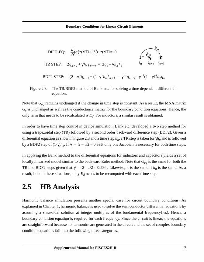
In order to have time step control in device simulation, Bank etc. developed a two step meth
using a trapezoidal step (TR) followed by a second order backward difference step (BDF2). G
differential equation as show in Figure 2.3 and a time stephn, a TR step is taken forγhn and is followed
by a BDF2 step of (1-γ)hn. If only one Jacobian is necessary for both time ste
In applying the Bank method to the differential equations for inductors and capacitors yields a
locally linearized model similar to the backward Euler method. Note thatGeq is the same for both the
TR and BDF2 steps given that . Likewise, it is the same ifhn is the same. As a
result, in both these situations, onlyEd needs to be recomputed with each time step.
2.5 HB Analysis
Harmonic balance simulation presents another special case for circuit boundary condition
explained in Chapter 1, harmonic balance is used to solve the semiconductor differential equat
assuming a sinusoidal solution at integer multiples of the fundamental frequency(ies). He
boundary condition equation is required for each frequency. Since the circuit is linear, the equ
are straightforward because no harmonics are generated in the circuit and the set of complex b
condition equations fall into the following three categories.
γ 2 2– 0.586≈=
tn tn+γ tn+1
γhn
hnDIFF. EQ:
tdd
q z t( )( )( ) f t z t( ),( )+ 0=
TR STEP: 2qn γ+ γ hn f n γ++ 2qn γ hn f n–=
BDF2 STEP: 2 γ–( )qn 1+ 1 γ–( )hn f n 1++ γ 1– qn γ+ γ 1– 1 γ–( )2hnqn–=
Figure 2.3 The TR/BDF2 method of Bank etc. for solving a time dependant differentialequation.
γ 2 2– 0.586≈=
Supplemental Manual for PISCES2H-B 7
Boundary Conditions for Linear Circuit Elements
similar
on the
trode of
e final
For the DC bias, the equation is determined by the methodology described previously.
(2.6)
For frequencies at which there is a source (i.e. the fundamental(s)) the equation is given in a
format except that it is complex.
(2.7)
Finally, for the harmonics generated by the nonlinear PISCES device, the equation takes
following form. Note that there is no generation term
(2.8)
The harmonic balance module computes the magnitude and phase of the current at each elec
the device for each frequency. That solution is then used in the circuit equations to compute th
circuit solution.
Gd0 Ed0 Vd0–( ) I d0 Ψ0 n0 p0, ,( )– 0=
Yd1 Ed1 Vd1–( ) I d1 Ψ1 n1 p1, ,( )– 0=
Edn
YdnVdn– I dn Ψn nn pn, ,( )– 0=
8 Supplemental Manual for PISCES2H-B
CHAPTER 3Models for QuantumMechanical Corrections andDynamic Trapping Effects
of the
ffects.
of the
ence of
he gate
ess to
annel
. The
the
or
(either
antum
l
g the
ening.
3.1 Introduction
This chapter describes two features in PISCES 2H-B, which are related to modeling
quantum mechanical effects in silicon MOS devices and analysis of dynamic trapping e
As the feature size of MOSFETs, mainly the gate length, keeps scaled down, the width
surface inversion layer becomes comparable to the gate oxide thickness. The consequ
this dimensionality closeness is that the gate capacitance is no longer determined by t
oxide only. To the first order, one can use an effective (or electrical) gate oxide thickn
model this thickness widening. Another effect of MOS scaling is the raise of the ch
doping in order to minimize the leakage current in the off-state of MOSFET operation
high doping level (typically above cm-3) increases the slope (i.e., steepness) of
surface potential well which is formed when MOS device is in either inversion
accumulation region. This steep potential well leads to the quantization of energy band
conduction or valence band depending on the operation region) due to the qu
mechanical effects in the normal direction to the Si/SiO2 interface. The ground energy leve
in the surface potential well is the lowest state for carriers to occupy, effectively shiftin
edge of the energy band. This effect can be modeled by the bandgap broad
317×10
Supplemental Manual for PISCES2H-B 9
Models for Quantum Mechanical Corrections and Dynamic Trapping Effects
by the
from
above
rating
wave
device
to the
ction
. The
ethod,
odel,
ormal
ccount
d the
unt of
each
amic
ses can
Furthermore, the carrier spacial density in the surface potential well is now determined
magnitude of the wavefunction, which results in the peak of carrier concentration away
the interface, on contrary to the prediction of classical physics. Even though, the
quantum mechanical (QM) effects can be modeled accurately in principle by incorpo
the SchrÖdinger equation solver in the conventional semiconductor equations, the
nature of particles and the involvement of eigenvalue problem deter this approach in
simulation,especially in the multi-dimensional cases. In stead, an incremental approach
macroscopic solution is much preferred. This approach calls for the introduction of corre
term(s) in the classical semconductor equations to partially include the QM effects
resulted equations still keeps main feature of the original equations and their solution m
but the solution will reflect the effect of QM corrections.
In PISCES 2H-B, there are three models available for QM corrections: the Hansch m
which gives the correct shape of carrier distribution in the channel region along the n
direction to the surface, van Dort model, which applies the bandgap broadening to a
for the QM effects but with a classical carrier distribution (peaking at the surface), an
hybrid model, which combines the above two models hence giving both correct amo
corrections and the shape of carrier distribution. We will first describe the theory for
approach and then give its usage.
Another feature to be described in this chapter is the simulation capability for dyn
trapping effects. By dynamic, it means that both the steady state and transient analy
be conducted.
10 Supplemental Manual for PISCES2H-B
Models for Quantum Mechanical Corrections and Dynamic Trapping Effects
) for
ier
carrier
met.
ith
of
nction,
m the
hes 0
carrier
n by
In Eq.
3.2 Models for Quantum Mechanical Corrections
3.2.1 Hansch Model
Realizing that quantum mechanical effects call for the repulsive boundary condition (BC
carrier distribution at the Si/SiO2 interface due to the existence of the potential barr
between SiO2 and silicon substrate, the Hansch model imposes a shape function to the
distribution in the direction normal to the interface such that the repulsive BC is
Specifically, it one assumes thatz-axis is along the normal direction to the interface, w
origin at the interface and positive direction towards the substrate, andx-axis is along the
channel, the carrier concentration (take electrons as an example) would take the form
(2.9)
where is the thermal characteristic length and represents how quickly the shape fu
which is the square bracketed part of the above equation, becomes unity away fro
interface ( ). is related to the barrier height between the SiO2 and Si and is different
for electrons from holes. When the barrier height becomes infinitely high, approac
and it means that the carrier concentration is zero at the interface. Otherwise, the
concentration at the interface has a finite value. is the carrier concentratio
applying classical physics, normally the drift-diffusion model. For Boltzmann statistics,
(2.10)
where is the thermal voltage and all other symbols have the conventional meaning.
(2.9) both and are related to the physical parameters as follows:
n x z,( ) nclassic x z,( ) 1 ez z0+( )2 λ2⁄–
–=
λ
z 0= z0z0
nclassic
nclassic nieψ φn–( ) Vt⁄
=
Vtλ z0
11 Supplemental Manual for PISCES2H-B
Models for Quantum Mechanical Corrections and Dynamic Trapping Effects
and
e for
tween
used
or the
nt
l and
same
ads to
(2.11)
(2.12)
where is the effective mass and is the potential barrier height for carriers, so
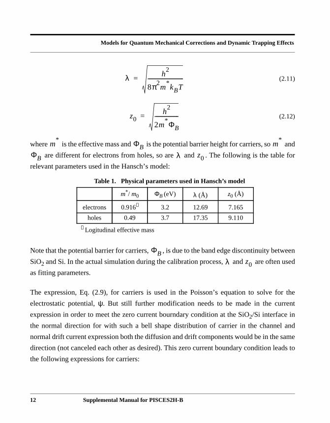
are different for electrons from holes, so are and . The following is the tabl
relevant parameters used in the Hansch’s model:
Note that the potential barrier for carriers, , is due to the band edge discontinuity be
SiO2 and Si. In the actual simulation during the calibration process, and are often
as fitting parameters.
The expression, Eq. (2.9), for carriers is used in the Poisson’s equation to solve f
electrostatic potential,ψ. But still further modification needs to be made in the curre
expression in order to meet the zero current bourndary condition at the SiO2/Si interface in
the normal direction for with such a bell shape distribution of carrier in the channe
normal drift current expression both the diffusion and drift components would be in the
direction (not canceled each other as desired). This zero current boundary condition le
the following expressions for carriers:
Table 1. Physical parameters used in Hansch’s model
m* / m0 ΦB (eV) λ (Å) z0 (Å)
electrons 0.916✝ 3.2 12.69 7.165
holes 0.49 3.7 17.35 9.110
✝ Logitudinal effective mass
λ h2
8π2m
*kBT
---------------------------=
z0h
2
2m* ΦB
------------------=
m* ΦB m
*
ΦB λ z0
ΦBλ z0
12 Supplemental Manual for PISCES2H-B
Models for Quantum Mechanical Corrections and Dynamic Trapping Effects
uantum
the
antum
e the
ersion
in the
he peak
rically,
o the
ck of
aning
on or
rm of
els in
the
(2.13)
The term added to in the square brackets in the above equations is often called the q
potential.
The advantage of Hansch’s model is it gives qualitatively correct carrier profile in
channel. But the drawback is that none of the parameters used to model the qu
corrections, and has any bias dependence, which makes it difficult to reproduc
measured device characteristics at all bias range (i.e., from the accumulation to inv
region). Later on we’ll discuss a way to improve the accuracy of this model.
3.2.2 van Dort Model
This model tries to capture the QM effects using the broadening of the bandgap
substrate surface region. Because both the energy band quantization and the shift of t
in channel carrier profile in the normal direction to the SiO2/Si interface away from the
interface amount to the increase of the effective bandgap in the surface region elect
van Dort model is quite successful in providing close simulation results compared t
measured data (mainly C-V characteristics including threshold voltage). The drawba
this model is that the carrier distribution in the channel still has the classical shape, me
it peaks at the surface of the substrate. The following is the model description.
Assuming a triangular potential well at the substrate surface during either inversi
accumulation region, the eigenfunctions to the Schrödinger equation have analytical fo
so-called Airy function and the eigenvalues which represent the quantized energy lev
the well are function of the slope of the potential well, which in turn is determined
jn qµnn∇ ψkBT
q---------- 1 e
z z0 n,+( )2 λn2⁄
– ln+– kBTµn∇n+=
j p qµpp∇ ψkBT
q---------- 1 e
z z0 p,+( )2 λp2⁄
– ln–– kBTµp∇p–=
ψ
λ z0
13 Supplemental Manual for PISCES2H-B
Models for Quantum Mechanical Corrections and Dynamic Trapping Effects
nd the
n the
verse
found
ith
lation
ually
trate
5),
s that
been
of
eters
strate
ess [2].
transverse surface electric field. Considering only the ground energy level in the well a
peak shift for the eigenfunction corresponding to the ground level, one can obtai
following relationship between the effective bandgap increase with the surface trans
electric field:
(2.14)
where is the surface transverse field and is a proportionality factor which can be
from the theory [1]. In PISCES, eV, where is a fitting parameter w
value unity or bigger. The effect of the bandgap broadening is included in the simu
through the intrinsic carrier concentration in the following way in order to have a grad
diminishing QM corrections when moving away from the surface towards the subs
contact.
(2.15)
where is a smooth function with form of
(2.16)
and with a characteristic length with typical value of 250Å. In Eq. (2.1
is the intrinsic carrier concentration using the conventional bandgap and i
using the bandgap with correction (i.e., addition) of Eq. (2.14). The van Dort model has
successfully applied to the calibration of 0.18µm CMOS process with gate oxide thickness
around 30Å. With both the polysilicon gate doping concentration and as fitting param
the C-V characteristics from the accumulation to inversion region and with different sub
bias can be simulated accurately. The optimal value of seems 1.7 for the above proc
∆Eg139------β
εSi
4kT----------
1 3⁄
FS2 3⁄
=
FS ββ 4.1
8–×10 κ= κ
ni niconv
1 g z( )–[ ] g z( )niQM
+=
g z( )
g z( ) 2ea2–
1 e2a2–
+
----------------------=
a z σ⁄= σni
convni
QM
κ
κ
14 Supplemental Manual for PISCES2H-B
Models for Quantum Mechanical Corrections and Dynamic Trapping Effects
orating
hese
ed by
hange
well.
shold
of the
which
ulation
into
and
ere are
ch in
ture of
strate.
of
wn that
.
th the
t from
ted in
shape
of the
ue to
3.2.3 Hybrid QM correction Model
While both Hansch’s model and van Dort model achieve reasonable success in incorp
the QM effects in the classical transport modeling framework, each has its limitations. T
limitations mainly stem from the incompleteness in capturing the physical picture caus
the quantum mechanical effects. For example, while Hansch model accounts for the c
of carrier profile in the channel due to the repulsive boundary condition at the SiO2/Si
interface, it fails to model the quantization of the energy band in the surface potential
So often Hansch’s model does not provide enough correction in predicting the thre
voltage, which is closely related to the bandgap. Also, as mentioned previously, none
paramters in this model has bias (mainly the surface transverse field) dependence,
leads to the failure in predicting the trend of the gate capacitance in the deep accum
region for nMOS structure. On the other hand, van Dort model indeed takes
consideration both the band quantization and shifting of peak in carrier doping profile
hence gives fairly accurate simulated C-V characteritics in the entire bias range. But th
two serious shortcomings with this model. First, the model uses over-simplified approa
lumpping all two effects in the increase of the bandgap, thus preserving the classic pic
the carrier profile, i.e., the peak of the channel carriers is on the surface of the sub
Secondly, model Eq. (2.14) implies the sigularity for when the derivative
channel charge is to be evaluated, which is needed in C-V simulation. It has been sho
the simulated C-V curve shows a spurious spike at the flatband region where
Furthermore, In all two models, in order to match the simulation results more closely wi
measured data, fitting parameters often end up with values which are quite differen
their physically meaningful defaults.
In view of all those shortcomings, a hybrid model has been developed and implemen
PISCES. This model essentially blends the previous two models by incorporating both
function, Eq. (2.9), and bandgap broadening, Eq. (2.14). In doing so, all major aspects
QM effects in MOS structure: band quantization and the bell shape of carrier profile d
FS 0=
FS 0=
15 Supplemental Manual for PISCES2H-B
Models for Quantum Mechanical Corrections and Dynamic Trapping Effects
ss the
new
inate
ause
vior of
and
, the
range
re the
of the
the
eature
om the
the superposition of eigenfunctions, are taken into consideration in the model. To addre
singularity problem of capacitance calculation intrinsic to van Dort model, Eq. (2.14), a
formula is proposed [3]:
(2.17)
where are two adustable paramters. The purpose of this modification is to elim
the singularity in evaluating the derivative of Eq. (2.14) with respect to (w.r.t.) (bec
of the presence of nonzero ) and at the same time to preserve the asymptotic beha
Eq. (2.14) when . The default values used in PISCES is
.
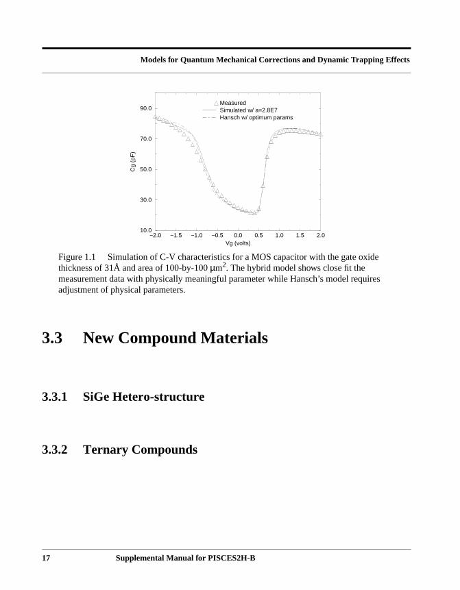
Applying this hybrid model to a MOS capacitor with the gate oxide thickness of 31Å
simulated C-V characteristics agree with the measured data very well for the entire bias
and there is no glitch in the flatband region as van Dort model often renders. Furthermo
model parameters used in the fitting are either all physical values (for Hansch’s part
model) or close to what theory predicts ( for van Dort’s part of the model while
theoretical value is 1.) And the simulated carrier profile in the channel preserves the f
mandated by the quantum mechanics: the peak of the channel carrier profile is away fr
SiO2/Si interface. This example of simulation is shown in Figure 1.1.
∆Eg139------β
εSi
4kBT-------------
1 3⁄ FS
2
c1eFS
2 c22⁄–
FS4 3⁄
+
------------------------------------------=
c1 c2,FS
c1FS ∞±→ c1 1
7×10=
c2 16×10=
κ 1.3=
16 Supplemental Manual for PISCES2H-B
Models for Quantum Mechanical Corrections and Dynamic Trapping Effects
3.3 New Compound Materials
3.3.1 SiGe Hetero-structure
3.3.2 Ternary Compounds
−2.0 −1.5 −1.0 −0.5 0.0 0.5 1.0 1.5 2.0Vg (volts)
10.0
30.0
50.0
70.0
90.0
Cg
(pF
)
MeasuredSimulated w/ a=2.8E7Hansch w/ optimum params
Figure 1.1 Simulation of C-V characteristics for a MOS capacitor with the gate oxidethickness of 31Å and area of 100-by-100µm2. The hybrid model shows close fit themeasurement data with physically meaningful parameter while Hansch’s model requiresadjustment of physical parameters.
17 Supplemental Manual for PISCES2H-B
Models for Quantum Mechanical Corrections and Dynamic Trapping Effects
3.3.3 Quaternary Compounds
3.4 Dynamic Trapping Analysis
18 Supplemental Manual for PISCES2H-B
CHAPTER 4Improved NumericalTechniques for High FrequencyAnalysis, Newton Projections,and One DimensionalSimulations
t three
CES to
o better
uickly
4.1 Introduction
This chapter discusses numerical improvements in PISCES2H-B. The improvements targe
separate areas. First, an improved algorithm for high frequency analysis is incorporated in PIS
improve the robustness of those solutions. Second, improvements in Newton projections lead t
initial guesses and algorithms for curve tracing. A one dimensional mode provides an option to q
analyze a device before a costly two dimensional run is executed.
4.2 High Frequency Analysis
4.3 Newton Projections
Supplemental Manual for PISCES2H-B 11

Improved Numerical Techniques for High Frequency Analysis, Newton
4.4 One Dimensional Mode
12 Supplemental Manual for PISCES2H-B
CHAPTER 5Users Manual
ilities. In
ircuit
circuit
lance
ults in
n and
to the
ar to
e the
SCES
5.1 IntroductionNew parameters and new cards were added to the PISCES in order to access the new capab
addition, for circuit boundary conditions, a SPICE like input deck is required to describe the c
configuration. This chapter describes the new PISCES cards and parameters as well as the
description input net list.
5.2 PISCES Card Additions
The improvements from PISCES-2H to PISCES 2H-B involves additions for harmonic ba
simulation, circuit boundary conditions, new models, and improved numerics. Each change res
new parameters in order to invoke the capability. In addition, harmonic balance simulatio
dynamic traps necessitate the addition of two cards.hbmeth (standing for HB method) is used to
define the parameters for the numerics involved in harmonic balance simulation and is similar
method card.trap is used to define profiles for the traps within the device structure and is simil
theprofile card. In addition, a separate file containing a SPICE-like net list is required to describ
circuit surrounding the PISCES device. The format for this file is described after the new PI
parameters and cards are categorized.
Supplemental Manual for PISCES2H-B 13
Users Manual
the
ing
the
COMMAND CONTACT
A new parameter is introduced for this card to allow the specification of
file containing the netlist of the surrounding circuit of the device be
simulated.
SYNTAX
Contact cktfile = <filename>
NEW PARAMETERS
cktfile
This parameters specifies the input file that contains the net list for
linear circuit surrounding the device.
EXAMPLE
contact cktfile=myckt.ckt
14 Supplemental Manual for PISCES2H-B
Users Manual
onic
fore
in. A
ctice
his
ery
).
COMMAND HBMETH
This new card specifies numerical limits and methods for the harm
balance module. It is similar in nature to themethod card.
SYNTAX
hbmeth [maxiter = <integer>] [useredpc] [krtol = <real>]
+ [kriter = <integer>] [gmrestart = <integer>]
+ [pkthresh = <real>] [gmrthresh = <real>]
+ [krloosetol = <real> krlooseiter = <integer>]
+ [krconvratio = <real>]
PARAMETERS
maxiter
This parameter specifies the maximum number of Newton iterations be
the HB simulator aborts and steps the voltage sources down to try aga
reasonable value is 30 although a good number is not known in pra
(Default: 30).
useredpc
This logical variable is used to specify the ‘reduced’ pre-conditioner. T
parameter is needed only for two-tone problems with very tightly or v
widely spaced tones and reduces memory dramatically (Default: false
Supplemental Manual for PISCES2H-B 15
Users Manual
ov)
and
ring
step
ake
ore
be
alue
large
large
d
krtol
This real variable specifies the tolerance for the iterative linear (Kryl
solves during the Newton process. Reasonable values are
(Default: ).
kriter
This integer parameter specifies the maximum number of iterations du
the iterative linear solve before it gives up and just takes the Newton
anyway. A value of 30-50 is reasonable (Default: 40).
gmrestart
This integer parameter is the number of iterations that GMRES will t
before “restarting.” In theory, the higher this number is, the faster and m
robust the linear solve will be. However, an additional vector has to
stored for each GMRES iteration, so its value cannot be too large. A v
of 10 tends to work well (Default: 10).
pkthresh
This real parameter is used to reduce Jacobian memory storage for
problems. Spectral components of less than (pkthresh * DC_value) are
dropped (Default: 0.0).
gmrthresh
This real parameters is used to reduce GMRES memory storage for
problems. GMRES vector entries of less thangmrthresh are dropped
(Default: 0.0).
krloosetol
This real parameter is used jointly with an integer parameterkrlooseiter
to be described next. Ifkrlooseiter GMRES iterations are completed an
1 3–×10
1 4–×10 1 4–×10
16 Supplemental Manual for PISCES2H-B
Users Manual
.
ter
e
f this
d and
e. In
tion
the GMRES error is belowkrloosetol , then the GMRES iterations are
considered adequate for proceeding with a Newton step (Default: 0.1)
krlooseiter
This integer parameter is used jointly with above real parame
krloosetol . If krlooseiter GMRES iterations are completed and th
GMRES error is belowkrloosetol , then the GMRES iterations are
considered adequate for proceeding with a Newton step (Default: 30).
krconvratio
When the ratio between two successive GMRES reaches the value o
real parameter, GMRES assumes progress toward a solution is stalle
therefore aborts (Default: 1.0).
EXAMPLE
hbmeth krtol=5e-4 kiter=35 ^useredpc
To specify the parameters used in harmonic balance simulation mod
this case, the maximum number of iterations in solving the linear equa
system using Krylov iterative method is 35 (kiter ). The tolerance for
convergence in Krylov iteration is set to (krtol ). And no “reduced”
pre-conditioner is used (^useredpc ).
5 4–×10
Supplemental Manual for PISCES2H-B 17
Users Manual
the
. It
tage
f the
for
o
th a
le for
fault:
file
at
COMMAND LOG
The following new parameters in this card allow for the storage of
circuit solution which is independent of the device solution.
SYNTAX
log cktfile=<filename> [column.out | spice.out | key.out]
NEW PARAMETERS
cktfile
This parameter specifies the output file name for the circuit solution
contains the voltage at each circuit node, the current through all vol
sources and inductors, and the current flowing into each electrode o
numerical device including any scaling factors. The default format
saved data iscolumn.out (Default: null character string, meaning n
circuit solution will be saved).
column.out
This logic flag forces the output data to be organized column-wise wi
heading describing the data in each column. This data format is suitab
post-processing by many general plotting tools and spreadsheets (De
True).
spice.out
This logic flag forces the data to be saved in a Berkeley SPICE-like raw
format. For those with access to Berkeley’s plotting tools, this form
18 Supplemental Manual for PISCES2H-B
Users Manual
an
n
s.
mn
in
the
ult:
provides an easily accessible tool to analyze the circuit solution.spice.out
is only available foropckt , acckt , dcckt , or trckt (Default: False).
key.out
This logic flag forces the output data into two files. The first file has
extension of.dat added to thecktfile name and the second has a
extension of.key. The.dat file contains the simulation results in column
The .key contains a mapping of the solution variables to the colu
number in the.dat . This output format allows the user to plot the data
many general plotting tools by excluding the heading information in
data file which can cause problems with some plotting tools (Defa
False).
EXAMPLE
log cktfile=mydata.dat column.out
Save circuit solution in filemydata.dat with column-wise format.
log cktfile=mydata.raw spice.out
Save circuit solution in filemydata.raw with Spice raw file format.
log cktfile=mydata key.out
Save circuit solution in filesmydata.dat and mydata.key as
explained in above parameter description forkey.out .
Supplemental Manual for PISCES2H-B 19
Users Manual
COMMAND METHOD
The new parameters on themethod card allows for specification of the
new numerical capabilities in PISCES.
SYNTAX
method [New Parameters]
NEW PARAMETERS
EXAMPLES
20 Supplemental Manual for PISCES2H-B
Users Manual
ical
COMMAND MODEL
Themodel card has additions to specify one of the quantum mechan
model and the parameters that are associated with each.
SYNTAX
model [dort [] [] [] ] [hansch [] [] [] ]
NEW PARAMETERS
EXAMPLES
Supplemental Manual for PISCES2H-B 21
Users Manual
f
d to
ion.
onic
the
COMMAND SOLVE
Many parameters are added to thesolve card in order to take advantage o
the new capabilities in PISCES. A new set of parameters are provide
invoke the circuit boundary condition and the harmonic balance solut
In addition, solution input/output parameters are provided for the harm
balance results.
SYNTAX
solve [opckt || acckt || dcckt || trckt || acdcckt || hbckt]
+ [hboutfile=<filename> [savestep=<integer>]]
+ [hbinfile=<filename>]
PARAMETERS
opckt
Solves for the operating point on the circuit. (Default: False)
acckt
Solves the small signal ac circuit. This parameter requires a.ac card in the
circuit file.(Default: False)
dcckt
Solves the DC circuit for the values of the swept source(s) specified on
.dc card in the circuit file.(Default: False)
22 Supplemental Manual for PISCES2H-B
Users Manual
ard
ator.
fied
tion
ing
file
en a
ution
n is
trckt
Solves for the transient response of the circuit. This card requires a.tran
card in the circuit file. In addition thetranckt may be used in lieu of
trckt .(Default: False)
acdcckt
Solve the small signal ac circuit while sweeping DC source(s). This c
requires a.dc and.ac card in the circuit file. In additiondcacckt may be
used in lieu ofacdcckt . (Default: False)
hbckt
Solves the large signal ac circuit using the harmonic balance simul
This card requires the HB simulator module and the.hb analysis card in
the circuit file. A sweeping of the DC and/or AC source can be speci
with the.hbac and/or the.hbdc card in the circuit file. (Default: False)
hboutfile
The basis for the name of the file to store the solution at a given simula
point. To this name an extension of “.sol” is added for the data forΨ, n, and
p. An extension of “.trm” is added to the name for the data file contain
the terminal characteristics. A “.nds” extension is added for the data
containing the circuit node solutions.
savestep
During a sweep of a source in a harmonic balance simulation,savestep is
used to specify how often the harmonic balance solution is saved giv
file basis specified byhboutfile . At each integer multiple of the given
value, the last letter of the output file name is incremented and the sol
is saved to that file. A value of 0 means only the last completed solutio
saved. (Default: 0)
Supplemental Manual for PISCES2H-B 23

Users Manual
ance
fied
hbinfile
Use the given file name as the starting point for the next harmonic bal
simulation. This file contains the “.sol” extension and it must be speci
when the file name is given.
NEW EXAMPLE
solve acckt
solve hbckt hboutfile=hbsolnA hbsavestep=15
24 Supplemental Manual for PISCES2H-B
Users Manual
and
COMMAND TRAP
This new card is used in the specification of the traps inside the device
at interfaces. It has a similar format to that of theprofile card.
SYNTAX
trap [Parameters]
NEW PARAMETERS
EXAMPLES
Supplemental Manual for PISCES2H-B 25
Users Manual
circuit
ndard
ctrode
.
circuit
oked
ce
ps up
ramps
for the
t
ndary
. It
tion is
as
ecified in
value
5.3 The Circuit File
A separate circuit file is needed to specify the linear circuit surrounding the PISCES device. The
file contains a SPICE-like net list to describe the connections of the external circuitry. The sta
SPICE linear elements are provided along with a special element for specifying the ele
connections for the linear devices. The standard analysis capabilities are provided with the.op , .dc ,
.ac, and.tran cards. In addition there are specialty dot cards for the harmonic balance analysis
Thecontact card in PISCES contains a parameter which is used to specify the file name for the
file. Even if a circuit file is specified for boundary conditions, the boundary conditions are not inv
unless one of the circuit solves is specified on thesolve card. Therefore, the recommended sequen
of cards in PISCES is as follows:
solve init outfile=soln.initsolve v1=1.0 vstep=1.0 nstep=4 num=1solve v2=0.25 vstep=0.25 nstep=5 num=2solve v1=5.0 v2=1.5 outfile=soln.dcinitsolve opckt outfile=soln.opsolve trckt
In this sequence, an initial solution is computed and saved in the file soln.init. The next card ram
the voltage on electrode number one which could be a drain or collector. The third solve card
up the voltage on electrode two which could be a gate or base. The fourth card solves
approximate operating point and stores that solution. The fifthsolve card accesses the circui
boundary conditions and solves for the operating point solution with the inclusion of circuit bou
conditions. The finalsolve card specifies a transient simulation with circuit boundary conditions
could just as easily specify an ac, dc, or harmonic balance circuit analysis. When the simula
restarted or fails, one can now use theload card to restart from any location at which is solution h
been saved.
The next set of pages provides description of the elements and analyses cards that can be sp
the circuit file. At the end of the chapter some limitation on node numbers and information on
specifications is outlined for the user.
26 Supplemental Manual for PISCES2H-B

Users Manual
is
COMMAND COMMENT LINES
Any line with an* in the first column is considered a comment and
ignored during parsing.
* This is a comment
Supplemental Manual for PISCES2H-B 27

Users Manual
ard.
The
fined
COMMAND NUMERICAL DEVICE
Nxxxxxxxx N1 . . . Ni
The PISCES device is specified by the numerical device element c
xxxxxxxx uniquely identifies the device andN1 through Ni are the
numerical nodes to which the device is connected in the circuit.
number of node connections must equal the number of electrodes de
in the PISCES deck otherwise the simulation will abort.
Nldmos 14 3 0
28 Supplemental Manual for PISCES2H-B

Users Manual
or
h
t
d are
COMMAND STANDARD ELEMENTS
Rxxxxxxxx N1 N2 val
Lxxxxxxxx N1 N2 val
Cxxxxxxxx N1 N2 val
The the R, L, andC identifies the element as either a resistor, inductor,
capacitor respectively.N1 andN2 are the numeric node numbers to whic
the element is connected. Theval variable represents the value of tha
element. The standard MKS units can be used to specify values an
described later in this document.
Rfeeback 23 81 1e3
Lpackage 87 63 93n
Cintercon 9 38 2.33p
Supplemental Manual for PISCES2H-B 29
Users Manual
ork
.
, C,
ngth,
each
the
nly
ffect
COMMAND TRANSMISSION LINE
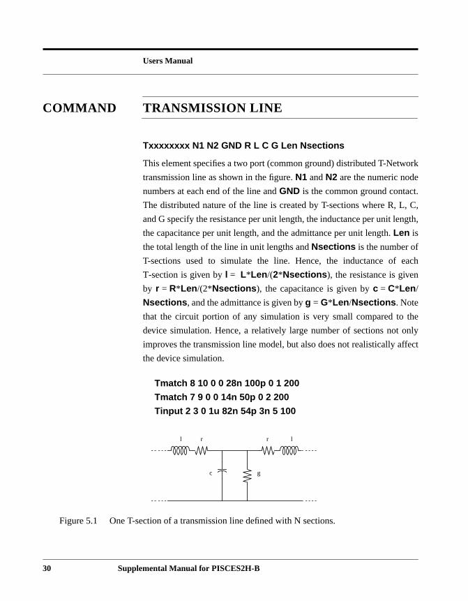
Txxxxxxxx N1 N2 GND R L C G Len Nsections
This element specifies a two port (common ground) distributed T-Netw
transmission line as shown in the figure.N1 andN2 are the numeric node
numbers at each end of the line andGND is the common ground contact
The distributed nature of the line is created by T-sections where R, L
and G specify the resistance per unit length, the inductance per unit le
the capacitance per unit length, and the admittance per unit length.Len is
the total length of the line in unit lengths andNsections is the number of
T-sections used to simulate the line. Hence, the inductance of
T-section is given byl = L*Len /(2*Nsections ), the resistance is given
by r = R*Len /(2*Nsections ), the capacitance is given byc = C*Len /
Nsections , and the admittance is given byg = G*Len /Nsections . Note
that the circuit portion of any simulation is very small compared to
device simulation. Hence, a relatively large number of sections not o
improves the transmission line model, but also does not realistically a
the device simulation.
Tmatch 8 10 0 0 28n 100p 0 1 200
Tmatch 7 9 0 0 14n 50p 0 2 200
Tinput 2 3 0 1u 82n 54p 3n 5 100
rl
c g
r l
Figure 5.1 One T-section of a transmission line defined with N sections.
30 Supplemental Manual for PISCES2H-B
Users Manual
ear
the
e
ain
ear
the
ols
ely.
COMMAND DEPENDENT SOURCES
Gxxxxxxxx N+ N- n+ n- val
Exxxxxxxx N+ N- n+ n- val
G andE specify a linear voltage controlled current source and a lin
voltage controlled voltage source.N+ and N- specify the positive and
negative nodes of the source. Current flows from the positive node to
negative node.n+ and n- specify the voltage nodes which control th
sources.val is the transconductance (in mhos) or the voltage g
respectively.
Fxxxxxxxx N+ N- Vname val
Hxxxxxxxx N+ N- Vname val
F and H specify a linear current controlled current source and a lin
current controlled voltage source.N+ and N- specify the positive and
negative nodes of the device. Current flows from the positive node to
negative node.Vname specifies the voltage source whose current contr
the devices.val is the current gain or transresistance (in ohms) respectiv
Gcond 0 12 20 0 1m
Egain 10 0 20 0 50
Fgain 0 40 32 33 12
Ftran 23 0 52 42 1k
Supplemental Manual for PISCES2H-B 31
Users Manual
rce
is
ode
for
ource
r
DC
ces.
the
COMMAND INDEPENDENT SOURCES
Vxxxxxxxx N+ N- <source description>
Ixxxxxxxx N+ N- <source description>
V and I specify an independent voltage source and current sou
respectively.N+ andN- are the numerical nodes to which the source
connected. Current flows from the positive node to the negative n
through the source.
The source descriptions are as follows. A voltage source is used
reference, but all descriptors can be used with a current source.
DC Sources
Vname 1 0 [dc] [value]
Thedc specifies the source as a DC source and the value is the given s
value. Neitherdc norvalue need to be specified. If onlyvalue is specified
then the source is assumed to be a DC source of that value. If neithedc
norvalue or if onlydc is specified then the source is assumed to be of
value zero.
Vgate 5 0 dc 2.3 Vcc 1 0 5.0
AC Sources
Vname 1 0 [dc] [DCvalue] ac [ACvalue]
Theac specifies this source as being AC and is required on all AC sour
ACvalue specifies the amplitude of the ac small signal generated by
32 Supplemental Manual for PISCES2H-B
Users Manual
lies a
ribed
here
e of
source. If no value is given,ACvalue is assumed to be 1.0. An optionaldc
specification may be place on the source to indicate that it also supp
DC bias.
Vperturb 5 0 dc 2.3 ac 0.1
Vinput 9 0 ac 0.6
TRANSIENT SOURCES
Vname 1 0 <transient source type>
Transient sources can take on a number of different function as desc
by the following functions.
Piece-wise Linear (pwl)
Vname 1 0 pwl t0 v0 t1 v1 t2 v2 t3 v3 . . .
Piece-wise linear sources are described by a discontinuous function w
each (time, voltage) point is connected by a linear change in the valu
the source. The points in the function are given as:
if t0 != 0 then the voltage at t=0 is set equal to the voltage at t = t0.
Vinput 10 0 pwl 0 0.0 1n 0.0 2n 0.5 10n 2.0 20n 2.0 21n 0.0
Time Value
t0 v0
t1 v1
t2 v2
... ...
Supplemental Manual for PISCES2H-B 33
Users Manual
ier
ear
Periodic Square Pulse (pulse)
Vname 1 0 pulse v1 v2 td tr tf pw per
A pulse is simply a piece-wise linear function specified in an eas
manner to define a periodic function. The variables are defined as:
and the function takes on the following values as a piece-wise lin
function:
Vname 1 0 pulse -0.5 0.5 10n 1n 1n 50n 100n
Variable Description
v1 initial value
v2 pulsed value
td time delay
tr rise time
tf fall time
pw pulse width
per period
Time Value
0.0 v1
td v1
td+tr v2
td+tr+pw v2
td+tr+pw+tf v1
per+td v1
per+td+tr v2
... ...
34 Supplemental Manual for PISCES2H-B

Users Manual
the
onic
Sinusoidal Function (sin)
Vname 1 0 sin Vo Va freq td theta
This source takes on the following sinusoidal functional values within
time ranges specified. Note that this does not define a source for harm
balance, but rather defines a source for transient analysis.
where:
Vname 1 0 sin 3.3 0.5 50Meg 0.0 0.0
Variable Description
Vo DC offset value
Va sinusoid amplitude
freq frequency in HZ
td delay time
theta damping factor
0 t td< < Vo
td t< Vo Va e t td–( )theta–( ) 2π freq t td+( )( )sin+
Supplemental Manual for PISCES2H-B 35
Users Manual
nal
Exponential Pulse (exp)
Vname 1 0 exp v1 v2 td1 tau1 td2 tau2
The exponential source takes on the following exponential functio
values within the time ranges specified.
where:
Vname 1 0 exp -1.5 0.75 3n 25n 50n 10
Variable Description
v1 initial value
v2 pulsed value
td1 rise delay time
tau1 rise time constant
td2 fall delay time
tau2 fall time constant
0 t td1< < V1
td1 t td2< < V1 V2 V1–( ) 1 et td1–( )–tau1
-----------------------–
–
+
td1 t td2< < V1 V2 V1–( ) 1 et td1–( )tau1
--------------------–
–
V1 V2–( ) 1 et td2–( )tau2
--------------------–
–
+ +
36 Supplemental Manual for PISCES2H-B
Users Manual
nal
ource
t a
s and
ysis.
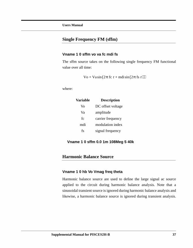
Single Frequency FM (sffm)
Vname 1 0 sffm vo va fc mdi fs
The sffm source takes on the following single frequency FM functio
value over all time:
where:
Vname 1 0 sffm 0.0 1m 108Meg 5 40k
Harmonic Balance Source
Vname 1 0 hb Vo Vmag freq theta
Harmonic balance source are used to define the large signal ac s
applied to the circuit during harmonic balance analysis. Note tha
sinusoidal transient source is ignored during harmonic balance analysi
likewise, a harmonic balance source is ignored during transient anal
Variable Description
Vo DC offset voltage
Va amplitude
fc carrier frequency
mdi modulation index
fs signal frequency
Vo Va 2π fc t mdi 2π fs t( )sin+( )sin+
Supplemental Manual for PISCES2H-B 37

Users Manual
ype.
ies:
All ac sources in the HB simulation must be specified with this source t
The parameters are defined as follows:
Hence the source takes on the following values for the given frequenc
Vname 1 0 hb 0.0 0.5 1.2G -90
Variable Description
Vo DC offset voltage
Vmag amplitude of sinusoid
freq frequency of sinusoid
theta phase of sinusoid (deg.)
Frequency Value
DC Vo
freq
0.0
Vm theta( )cos jVm theta( )sin+
n freq×
38 Supplemental Manual for PISCES2H-B
Users Manual
rcuit
ed in
o
but
e of
or no
.
the
ally
e of
uring
es the
COMMAND OPTIONS CARD
The.options card is used to set numerical parameters related to the ci
simulation.
SYNTAX
.options [gmin=value] [rmin=value] [area=value] [ltertol=value]
[ltevtol=value] [lteitol=value] [ltelim=value]
PARAMETER
gmin
Thegmin parameter specifies the smallest value for a conductance us
the circuit simulation. Agmin conductor is placed from every node t
ground. This additional large resistance adds a leakage current,
guarantees that the matrix is not singular. Note that too small a valu
gmin may cause ill- conditioning. For most applications,gmin could be
set to zero and hence, have no affect. However, if there are very few
passive components in the circuit,gmin has to be larger than zero
(Default: 1.0e-12 mhos).
rmin
Thermin parameter is used to specify a small resistance for places in
circuit where a small short-circuit is required. This resistance is typic
used for an inductor connecting a voltage source solely to an electrod
the PISCES device. Inductors are replaced with a zero volts source d
DC analysis and hence, a zero resistance in this situation can caus
Supplemental Manual for PISCES2H-B 39
Users Manual
t the
st
ld be
r is a
For
ugh
ation
s for
user
the
r by
ith
he
If the
dt is
rror
he
matrices to go singular. Likegmin , the effect ofrmin is minimal. Only a
small voltage is typically lost across the resistor and it guarantees tha
matrix is not singular. Thermin parameter can be set to zero for mo
cases, but should a matrix inversion error occur, this parameter shou
set to some small inconsequential value. (Default: 1.0e-12 ohms)
area
PISCES solves a device in only two dimensions. The area paramete
scaling factor for all currents in order to provide a quasi-3d solution.
most applications, this parameter refers to the width of the device altho
symmetry (like in BJT’s) could meanarea is equal to twice the device
length or more.
ltertol, ltevtol, lteitol, ltelim
These four parameters are used in the calculations of the local trunc
error during transient analysis. For most applications, the default value
these parameters are sufficient, but a brief description is provided for a
who may want to adjust the time step controls of the circuit portion of
simulation. For a more detailed description, please refer to the pape
Bank, etc.
ltertol : The relative tolerance for calculating the errors associated w
each time step. (Default: 0.001)
ltevtol : The absolute error tolerance for voltages. (Default: 1mV)
lteitol : The absolute error tolerance for currents. (Default: 1pA)
ltelim : The limit on the value for the norm of the error tolerance. If t
norm is greater than this value, the time step is reduced and repeated.
norm is less than this value, the time step is accepted and the next
calculated. (Default: 1.0)
In order to increase the accuracy in the overall solution, the relative e
tolerance (ltertol ) can be decreased. Likewise, in order to relax t
40 Supplemental Manual for PISCES2H-B
Users Manual
he
,
sis.
ence,
accuracy,ltertol is increased. In order to affect only the voltage or t
current,ltevtol or lteitol should be adjusted in the same manner asltertol .
Finally, in order to tighten the time steps,ltelim can be reduced or likewise
to relax the time steps ltelim is increased.
All these parameters only affect the circuit portion of the transient analy
In most cases, the device simulation tends to limit the time steps, and h
these parameters should rarely be changed.
EXAMPLES
.options gmin=0.0 rmin=0.0 area=100
Supplemental Manual for PISCES2H-B 41
Users Manual
and
d to
cards
ces
e the
ep
e,
equal
COMMAND ANALYSIS CARDS
A set of analysis cards provides the user a way to specify the limits
conditions on the different types of analysis. Note that PISCES is use
select the desired analysis via the solve card; hence, multiple analyses
can exist in one file.
Operating Point Simulation
.op
Compute the operating point solution.
DC Sweep Simulation
.dc Sname1 start1 end1 step1 [Sname2 start2 end2 step2]
The .dc card allows for the sweeping of DC sources. Up to two sour
may be swept simultaneously where the second source is swept insid
first source. The.dc requires at least one source and set of swe
parameters to be specified. Thestart parameters refers to the start valu
the end parameter refers to the end value, and thestep refers to the
stepping value. The source is stepped until its value is greater than or
to its end value.
.dc Vin 0.0 0.5 0.05
42 Supplemental Manual for PISCES2H-B
Users Manual
are
The
ient
e
time
DF
. The
The
be
qual
t is
AC Simulation
.ac [dec || lin] numsteps startf endf
The.ac card specifies a small signal sweep in frequency. All ac sources
swept over the specified frequencies as determined by this card.
sweeping can be linear or logarithmic as specified by thelin or dec
parameter. Thelin parameter means thenumsteps are taken linearly from
startf to endf . The dec parameter means thatnumsteps are taken
logarithmically and there arenumsteps per decade.
.ac lin 10 1k 10k
.ac dec 5 100k 1G
Transient Simulation
.tran tstep tstop [tstart tmax]
The .tran card specifies the time range and time steps for a trans
analysis. Thetstep parameter specifies the initial time step. If th
backward Euler method is selected on the PISCES method card, this
step is used throughout the entire PISCES/circuit simulation. If the B
method is selected on the PISCES method card, thentstep is the initial
time step and time step estimation is used to select all future values
tstop parameter specifies the time at which the simulation stops.
tstart parameter specifies the point in time from which the solution is to
saved. If this parameter is not given, the solution is saved from time e
to zero. Thetmax parameter is the maximum time step to be taken. If i
43 Supplemental Manual for PISCES2H-B
Users Manual
time.
lance
The
. The
s if
f
t.
not given, the maximum is calculated based upon the value of the stop
This ratio is set at compilation and has a default value of 0.1.
.tran 0.1n 25n
.tran 0.1n 25n 0.0 5n
Harmonic Balance Simulation
.hb f1 order [f2] [f3] [f4] . . .
.hbdc Sname start end step [Sname start end step] . . .
.hbac Sname start end step [Sname start end step] . . .
.hbfr Sname start end step fnum [Sname start end step] . . .
.hbss nstep a|d|f Sname start end {fnum} [a|d|f Sname . . .
These analysis cards are used to specify various types of harmonic ba
analysis. The.hb card is required and describes the Fourier expansion.
f1 parameter specifies the first fundamental frequency and is required
subsequentf# parameters specify the higher fundamental frequencie
inter-modulation distortion analysis is to be performed. Theorder
parameter is the number of harmonics used in the Fourier expansion.
The .hbdc , .hbac , .hbfr , and .hbss card specifies any sweeping o
sources. The.hbdc causes the HB sourceSname to have its DC bias
swept from thestart value to theend value instep steps. The sources
listed later on the card are swept inside the sources listed first.
The.hbac causes the HB sourceSname to have its large signal AC value
swept in magnitude fromstart value toend value instep steps. The
sources listed later on the card are swept inside the sources listed firs
The .hbfr card causes the HB sourceSname to have it frequency value
swept fromstart value to end value in step steps. In addition, the
fundament frequency numberfnum is adjusted to this value as well.
44 Supplemental Manual for PISCES2H-B

Users Manual
that
only
uch
z
tion
en
The .hbss allows for simultaneous sweeps of multiple sources such
the specified value is adjusted for each and every source. Therefore,
one value is specified for the number of steps,nstep . Each sourceSname
has either its ac magnitude, DC value, or frequency value (a | d | f) swept
from start value toend value with the samenstep steps. If frequency is
swept, then the fundamental value is adjusted as given byfnum .
Multiple cards may be contained in the same simulation. For s
situations, the sources on.hbss are swept inside the source on.hbfr which
are swept inside the sources on the.hbac card, which are swept inside the
sources on the.hbdc card.
.hb 1.2G 8
.hbac Vin 0.25 4.0 0.25
Sweep sourceVin from 0.25 to 4.0 by 0.25. Do a HB simulation at 1.2 GH
with 8 harmonics.
.hb 849.5Meg 5 850.5Meg
.hbss 16 Vin1 a 0.25 4.0 Vin2 a 0.25 4.0
Sweep the magnitude of the ac voltage ofVin1 andVin2 from 0.25 to 4.0
volts in 16 steps. Hence, during each stepVin1 andVin2 take on the same
value. This sweep description is designed to do inter-modulation distor
analysis by setting the frequency ofVin1 to 849.5MHz and that ofVin2 to
850.5MHz. The.hb card specifies a 5th order expansion at the two giv
frequencies.
45 Supplemental Manual for PISCES2H-B

Users Manual
alpha-
.3e-5,
5.4 NODE NUMBERS
The node numbers in the net list must be unique positive integers. Negative numbers and
numeric characters will cause an error.
5.5 SCALING FACTORS
The values in the net list may be specified in decimal notation (1.2), exponential notation (4
10e4) or using a scaling factor (1k). The scaling factors are defined as follows:
Unit Symbol Scaling
tera t 1012
giga g 109
mega meg 106
kilo k 103
centi c 10-2
milli m 10-3
micro u 10-6
nano n 10-9
pico p 10-12
femto f 10-15
atto a 10-18
46 Supplemental Manual for PISCES2H-B
CHAPTER 6Examples
e first
efficient
ted by
GaAs
ing a
takes
circuits
e first
he photo
ds are
6.1 Description
This chapter provides many examples of using the new features provided in PISCES2H-B. Th
section is devoted to examples that exercise the improved numerics and demonstrates more
convergence. In the following section, some applications for the new models are demonstra
showing the effect of quantum mechanics on MOS CV characteristics and the effect of traps in a
diode. The third section focuses on simulations with external boundary conditions by show
variety of different analysis methods. The final section gives a number of examples that
advantage of the harmonic balance module to find large signal responses of some common RF
including a demodulator, mixer, and power amplifier.
6.2 Examples Exercising the Improved Numerics
There are two examples that demonstrate the improvement in the numerics in PISCES. Th
example addresses the effect of newton projection on the convergence of a non-planar avalanc
diode. The second example involves a high frequency simulation of a _____. The new metho
capable of finding a solution whereas the old methods tended to struggle.
Supplemental Manual for PISCES2H-B 47
Examples
antum
ucture.
nation,
two of
6.2.1 Convergence in a Non-Planar Avalanche Photo Diode
6.2.2 High Frequency Analysis
6.3 Applications for the New Physical Models
Examples are provided for the three new models in PISCES. The first examples invoke the qu
mechanical models which are used to calculate the modified CV characteristics of a MOS str
The third example demonstrates the affect of dynamic traps in a GaAs diode.
6.3.1 C-V Characteristics Using van Dort QM Model
6.3.2 AC Analysis of MOSFET Using Hansch QM Model
6.3.3 Traps in a GaAs Diode
6.4 Circuit Boundary Conditions
6.4.1 Diode with External Circuit Components and DistributedContact Resistance
PISCES boundary conditions include distributed contact resistances, limited surface recombi
external resistances/capacitances, and linear circuit boundary conditions. This example uses
48 Supplemental Manual for PISCES2H-B
Examples
n order
rodes. In
circuit
owing
6.2b
d
d high
nitude
e
these boundary conditions simultaneously, contact resistance and circuit boundary condition, i
to the plot the IV characteristics of a diode with external resistances.
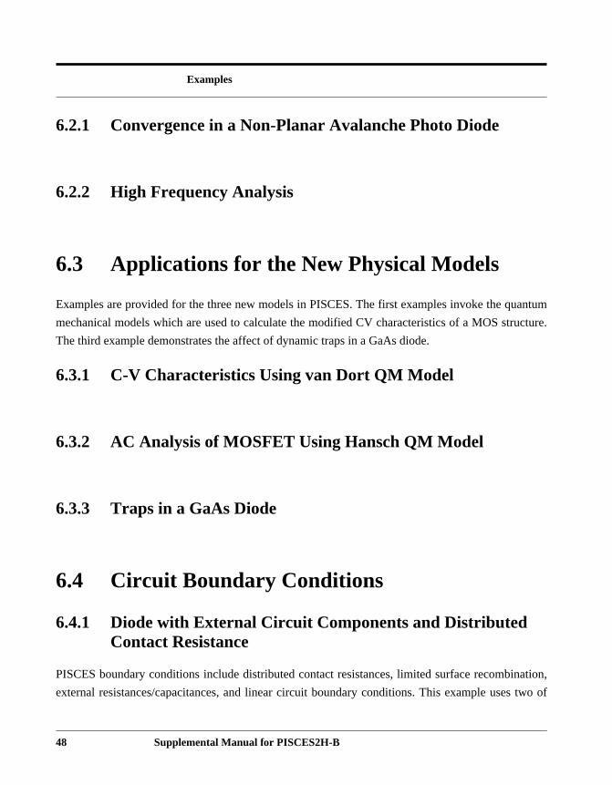
A diode has external resistors on each electrode and a feedback resistor between the two elect
addition, electrode two has a distributed contact resistance as shown in Figure 6.1 Next to the
diagram, the IV characteristics are given for the configuration. Note the large leakage current fl
through the feedback resistance.
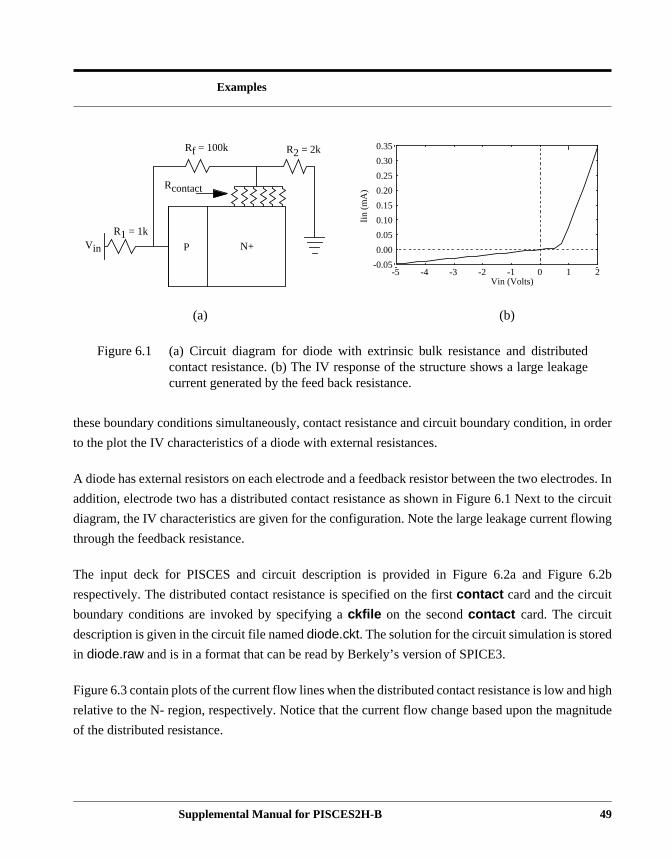
The input deck for PISCES and circuit description is provided in Figure 6.2a and Figure
respectively. The distributed contact resistance is specified on the firstcontact card and the circuit
boundary conditions are invoked by specifying ackfile on the secondcontact card. The circuit
description is given in the circuit file nameddiode.ckt. The solution for the circuit simulation is store
in diode.raw and is in a format that can be read by Berkely’s version of SPICE3.
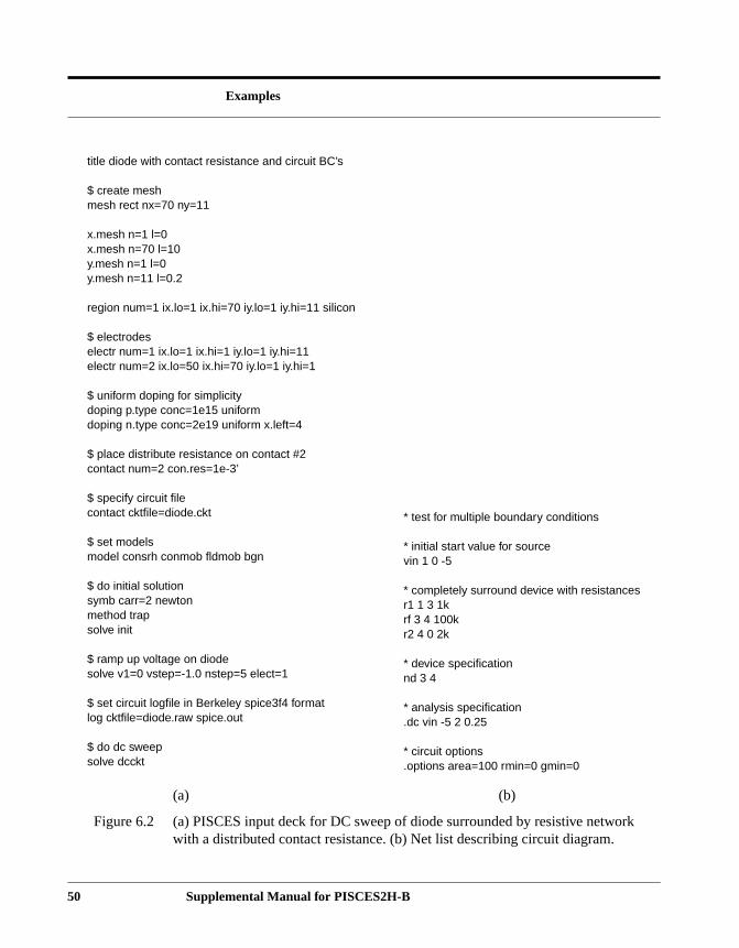
Figure 6.3 contain plots of the current flow lines when the distributed contact resistance is low an
relative to the N- region, respectively. Notice that the current flow change based upon the mag
of the distributed resistance.
R1 = 1k
Rf = 100k R2 = 2k
P N+
Rcontact
Vin
Figure 6.1 (a) Circuit diagram for diode with extrinsic bulk resistance and distributedcontact resistance. (b) The IV response of the structure shows a large leakagcurrent generated by the feed back resistance.
-0.05
0.00
0.05
0.10
0.15
0.20
0.25
0.30
0.35
-5 -4 -3 -2 -1 0 1 2Vin (Volts)
Iin (
mA
)
(a) (b)
Supplemental Manual for PISCES2H-B 49
Examples
k
title diode with contact resistance and circuit BC’s
$ create meshmesh rect nx=70 ny=11
x.mesh n=1 l=0x.mesh n=70 l=10y.mesh n=1 l=0y.mesh n=11 l=0.2
region num=1 ix.lo=1 ix.hi=70 iy.lo=1 iy.hi=11 silicon
$ electrodeselectr num=1 ix.lo=1 ix.hi=1 iy.lo=1 iy.hi=11electr num=2 ix.lo=50 ix.hi=70 iy.lo=1 iy.hi=1
$ uniform doping for simplicitydoping p.type conc=1e15 uniformdoping n.type conc=2e19 uniform x.left=4
$ place distribute resistance on contact #2contact num=2 con.res=1e-3’
$ specify circuit filecontact cktfile=diode.ckt
$ set modelsmodel consrh conmob fldmob bgn
$ do initial solutionsymb carr=2 newtonmethod trapsolve init
$ ramp up voltage on diodesolve v1=0 vstep=-1.0 nstep=5 elect=1
$ set circuit logfile in Berkeley spice3f4 formatlog cktfile=diode.raw spice.out
$ do dc sweepsolve dcckt
* test for multiple boundary conditions
* initial start value for sourcevin 1 0 -5
* completely surround device with resistancesr1 1 3 1krf 3 4 100kr2 4 0 2k
* device specificationnd 3 4
* analysis specification.dc vin -5 2 0.25
* circuit options.options area=100 rmin=0 gmin=0
Figure 6.2 (a) PISCES input deck for DC sweep of diode surrounded by resistive networwith a distributed contact resistance. (b) Net list describing circuit diagram.
(a) (b)
50 Supplemental Manual for PISCES2H-B
Examples
at are
6.4.2 Transient Response of a BJT Inverter
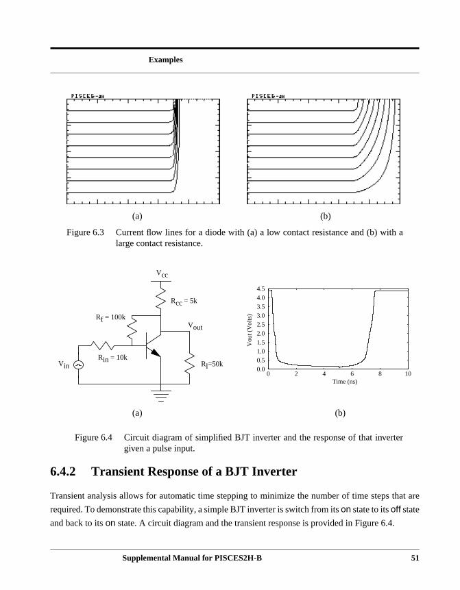
Transient analysis allows for automatic time stepping to minimize the number of time steps th
required. To demonstrate this capability, a simple BJT inverter is switch from itson state to itsoff state
and back to itson state. A circuit diagram and the transient response is provided in Figure 6.4.
Figure 6.3 Current flow lines for a diode with (a) a low contact resistance and (b) with alarge contact resistance.
(a) (b)
Vcc
VinRin = 10k
Rcc = 5k
Rf = 100kVout
Rl=50k
Figure 6.4 Circuit diagram of simplified BJT inverter and the response of that invertergiven a pulse input.
0.0
0.5
1.0
1.5
2.0
2.5
3.0
3.5
4.0
4.5
0 2 4 6 8 10
Vou
t (V
olts
)
Time (ns)
(a) (b)
Supplemental Manual for PISCES2H-B 51
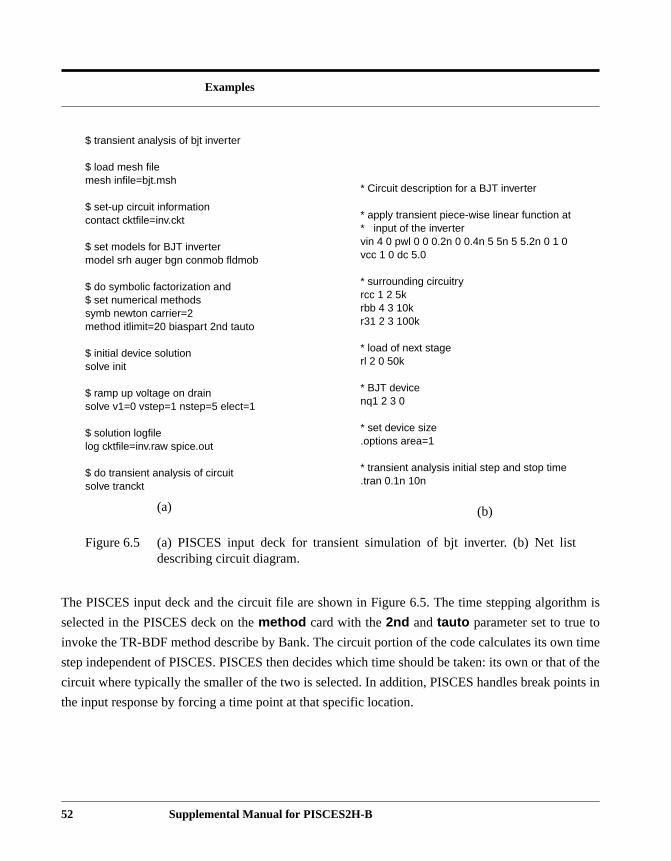
Examples
hm is
time
t of the
ints in
The PISCES input deck and the circuit file are shown in Figure 6.5. The time stepping algorit
selected in the PISCES deck on themethod card with the2nd andtauto parameter set to true to
invoke the TR-BDF method describe by Bank. The circuit portion of the code calculates its own
step independent of PISCES. PISCES then decides which time should be taken: its own or tha
circuit where typically the smaller of the two is selected. In addition, PISCES handles break po
the input response by forcing a time point at that specific location.
$ transient analysis of bjt inverter
$ load mesh filemesh infile=bjt.msh
$ set-up circuit informationcontact cktfile=inv.ckt
$ set models for BJT invertermodel srh auger bgn conmob fldmob
$ do symbolic factorization and$ set numerical methodssymb newton carrier=2method itlimit=20 biaspart 2nd tauto
$ initial device solutionsolve init
$ ramp up voltage on drainsolve v1=0 vstep=1 nstep=5 elect=1
$ solution logfilelog cktfile=inv.raw spice.out
$ do transient analysis of circuitsolve tranckt
* Circuit description for a BJT inverter
* apply transient piece-wise linear function at* input of the invertervin 4 0 pwl 0 0 0.2n 0 0.4n 5 5n 5 5.2n 0 1 0vcc 1 0 dc 5.0
* surrounding circuitryrcc 1 2 5krbb 4 3 10kr31 2 3 100k
* load of next stagerl 2 0 50k
* BJT devicenq1 2 3 0
* set device size.options area=1
* transient analysis initial step and stop time.tran 0.1n 10n
Figure 6.5 (a) PISCES input deck for transient simulation of bjt inverter. (b) Net listdescribing circuit diagram.
(a) (b)
52 Supplemental Manual for PISCES2H-B
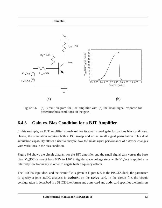
Examples
tions.
is dual
anges
e base
meter
6.4.3 Gain vs. Bias Condition for a BJT Amplifier
In this example, an BJT amplifier is analyzed for its small signal gain for various bias condi
Hence, the simulation requires both a DC sweep and an ac small signal perturbation. Th
simulation capability allows a user to analyze how the small signal performance of a device ch
with variations in the bias condition.
Figure 6.6 shows the circuit diagram for the BJT amplifier and the small signal gain versus th
bias. Vin(DC) is swept from 0.5V to 1.0V in tightly space voltage steps while Vin(ac) is applied at a
relatively low frequency in order to negate high frequency effects.
The PISCES input deck and the circuit file is given in Figure 6.7. In the PISCES deck, the para
to specify a joint ac/DC analysis isacdcckt on thesolve card. In the circuit file, the circuit
configuration is described in a SPICE-like format and a.ac card and a.dc card specifies the limits on
Vcc
Vin(DC)
Vin(ac) Rin = 50k
Rcc= 75k
Rf = 10M
Vout
05
101520253035404550
0.5 0.55 0.6 0.65 0.7 0.75 0.8 0.85 0.9 0.95 1
Vin(DC) (Volts)V
out(a
c)/V
in(a
c) (
Vol
ts)
Figure 6.6 (a) Circuit diagram for BJT amplifier with (b) the small signal response fordifference bias conditions on the gate.
(b)(a)
Supplemental Manual for PISCES2H-B 53
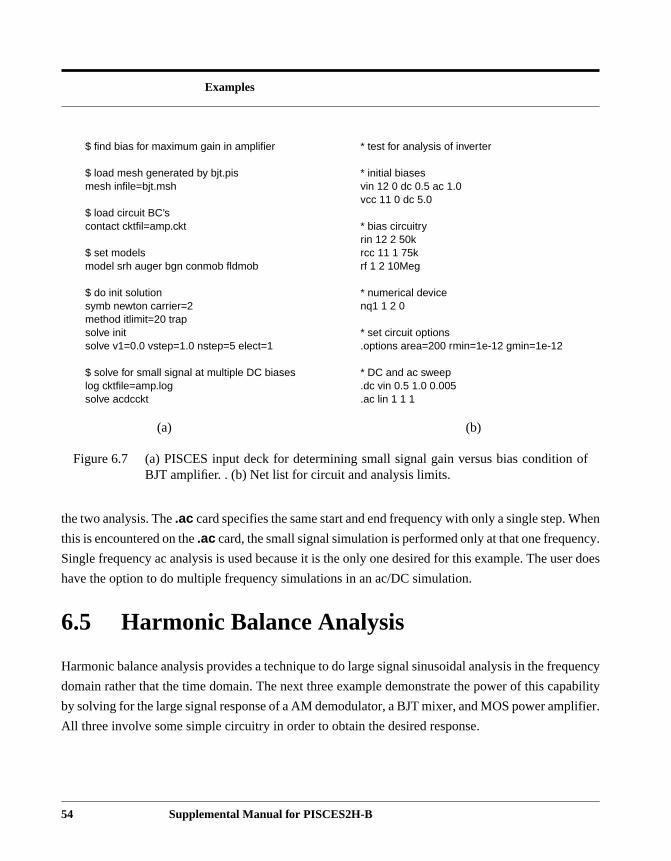
Examples
When
ncy.
ser does
quency
pability
lifier.
of
the two analysis. The.ac card specifies the same start and end frequency with only a single step.
this is encountered on the.ac card, the small signal simulation is performed only at that one freque
Single frequency ac analysis is used because it is the only one desired for this example. The u
have the option to do multiple frequency simulations in an ac/DC simulation.
6.5 Harmonic Balance Analysis
Harmonic balance analysis provides a technique to do large signal sinusoidal analysis in the fre
domain rather that the time domain. The next three example demonstrate the power of this ca
by solving for the large signal response of a AM demodulator, a BJT mixer, and MOS power amp
All three involve some simple circuitry in order to obtain the desired response.
$ find bias for maximum gain in amplifier
$ load mesh generated by bjt.pismesh infile=bjt.msh
$ load circuit BC’scontact cktfil=amp.ckt
$ set modelsmodel srh auger bgn conmob fldmob
$ do init solutionsymb newton carrier=2method itlimit=20 trapsolve initsolve v1=0.0 vstep=1.0 nstep=5 elect=1
$ solve for small signal at multiple DC biaseslog cktfile=amp.logsolve acdcckt
* test for analysis of inverter
* initial biasesvin 12 0 dc 0.5 ac 1.0vcc 11 0 dc 5.0
* bias circuitryrin 12 2 50krcc 11 1 75krf 1 2 10Meg
* numerical devicenq1 1 2 0
* set circuit options.options area=200 rmin=1e-12 gmin=1e-12
* DC and ac sweep.dc vin 0.5 1.0 0.005.ac lin 1 1 1
Figure 6.7 (a) PISCES input deck for determining small signal gain versus bias conditionBJT amplifier. . (b) Net list for circuit and analysis limits.
(a) (b)
54 Supplemental Manual for PISCES2H-B
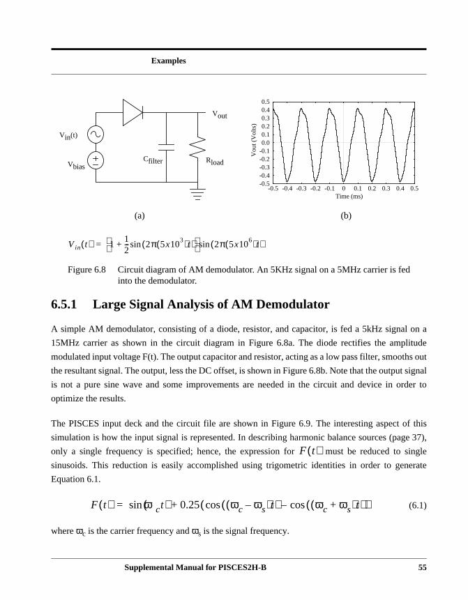
Examples
l on a
litude
ths out
t signal
rder to
of this
ge 37),
single
erate
6.5.1 Large Signal Analysis of AM Demodulator
A simple AM demodulator, consisting of a diode, resistor, and capacitor, is fed a 5kHz signa
15MHz carrier as shown in the circuit diagram in Figure 6.8a. The diode rectifies the amp
modulated input voltage F(t). The output capacitor and resistor, acting as a low pass filter, smoo
the resultant signal. The output, less the DC offset, is shown in Figure 6.8b. Note that the outpu
is not a pure sine wave and some improvements are needed in the circuit and device in o
optimize the results.
The PISCES input deck and the circuit file are shown in Figure 6.9. The interesting aspect
simulation is how the input signal is represented. In describing harmonic balance sources (pa
only a single frequency is specified; hence, the expression for must be reduced to
sinusoids. This reduction is easily accomplished using trigometric identities in order to gen
Equation 6.1.
(6.1)
whereωc is the carrier frequency andωs is the signal frequency.
Vbias
Vin(t)
Cfilter Rload
Vout
Vin t( ) 112--- 2π 5x10³( )t( )sin+
2π 5x10⁶( )t( )sin=
Figure 6.8 Circuit diagram of AM demodulator. An 5KHz signal on a 5MHz carrier is fedinto the demodulator.
-0.5-0.4-0.3-0.2-0.10.00.10.20.30.40.5
-0.5 -0.4 -0.3 -0.2 -0.1 0 0.1 0.2 0.3 0.4 0.5Time (ms)
Vou
t (V
olts
)
(a) (b)
F t( )
F t( ) ωct( )sin 0.25 ωc ωs–( )t( )cos ωc ωs+( )t( )cos–( )+=
Supplemental Manual for PISCES2H-B 55
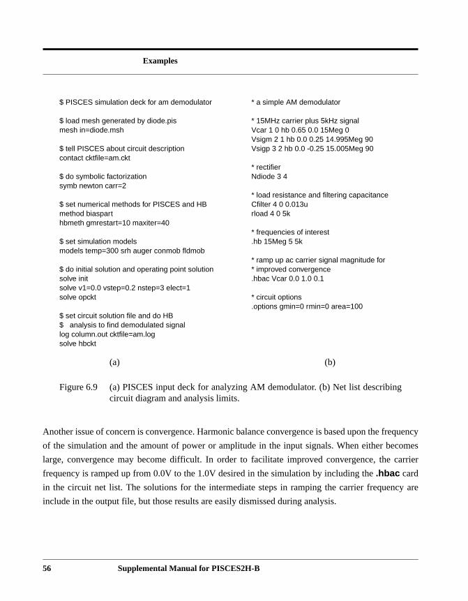
Examples
equency
comes
arrier
cy are
Another issue of concern is convergence. Harmonic balance convergence is based upon the fr
of the simulation and the amount of power or amplitude in the input signals. When either be
large, convergence may become difficult. In order to facilitate improved convergence, the c
frequency is ramped up from 0.0V to the 1.0V desired in the simulation by including the.hbac card
in the circuit net list. The solutions for the intermediate steps in ramping the carrier frequen
include in the output file, but those results are easily dismissed during analysis.
$ PISCES simulation deck for am demodulator
$ load mesh generated by diode.pismesh in=diode.msh
$ tell PISCES about circuit descriptioncontact cktfile=am.ckt
$ do symbolic factorizationsymb newton carr=2
$ set numerical methods for PISCES and HBmethod biasparthbmeth gmrestart=10 maxiter=40
$ set simulation modelsmodels temp=300 srh auger conmob fldmob
$ do initial solution and operating point solutionsolve initsolve v1=0.0 vstep=0.2 nstep=3 elect=1solve opckt
$ set circuit solution file and do HB$ analysis to find demodulated signallog column.out cktfile=am.logsolve hbckt
* a simple AM demodulator
* 15MHz carrier plus 5kHz signalVcar 1 0 hb 0.65 0.0 15Meg 0Vsigm 2 1 hb 0.0 0.25 14.995Meg 90Vsigp 3 2 hb 0.0 -0.25 15.005Meg 90
* rectifierNdiode 3 4
* load resistance and filtering capacitanceCfilter 4 0 0.013urload 4 0 5k
* frequencies of interest.hb 15Meg 5 5k
* ramp up ac carrier signal magnitude for* improved convergence.hbac Vcar 0.0 1.0 0.1
* circuit options.options gmin=0 rmin=0 area=100
Figure 6.9 (a) PISCES input deck for analyzing AM demodulator. (b) Net list describingcircuit diagram and analysis limits.
(a) (b)
56 Supplemental Manual for PISCES2H-B
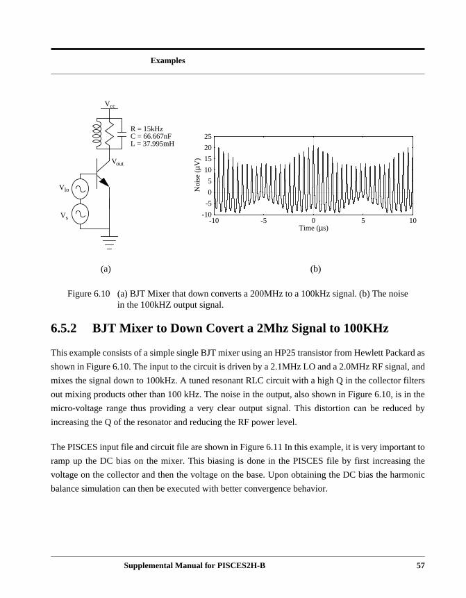
Examples
ard as
l, and
ilters
in the
ed by
nt to
g the
rmonic
6.5.2 BJT Mixer to Down Covert a 2Mhz Signal to 100KHz
This example consists of a simple single BJT mixer using an HP25 transistor from Hewlett Pack
shown in Figure 6.10. The input to the circuit is driven by a 2.1MHz LO and a 2.0MHz RF signa
mixes the signal down to 100kHz. A tuned resonant RLC circuit with a high Q in the collector f
out mixing products other than 100 kHz. The noise in the output, also shown in Figure 6.10, is
micro-voltage range thus providing a very clear output signal. This distortion can be reduc
increasing the Q of the resonator and reducing the RF power level.
The PISCES input file and circuit file are shown in Figure 6.11 In this example, it is very importa
ramp up the DC bias on the mixer. This biasing is done in the PISCES file by first increasin
voltage on the collector and then the voltage on the base. Upon obtaining the DC bias the ha
balance simulation can then be executed with better convergence behavior.
Vout
Vlo
Vs
R = 15kHzC = 66.667nFL = 37.995mH
Vcc
-10
-5
0
5
10
15
20
25
-10 -5 0 5 10
Noi
se (µ
V)
Time (µs)
Figure 6.10 (a) BJT Mixer that down converts a 200MHz to a 100kHz signal. (b) The noisein the 100kHZ output signal.
(a) (b)
Supplemental Manual for PISCES2H-B 57

Examples
rovide
MOS
rasitics
ifier is
m the
t by an
6.5.3 Analyzing Gain and Efficiency in a MOS Power Amplifier
The modeling of an RF device coupled with parastics, matching network, and bias network can p
insight into the performance of a discrete power amplifier. Figure 6.12 shows the intrinsic LD
device with parastics at the chip level due to the pad and interconnect. In addition to the pa
shown, there are additional parasitics for the packaging. The input and output of the ampl
connected through matching networks that are tuned for the individual device and isolated fro
DC bias by a capacitor. A biasing network sets the operating point and is isolated from the inpu
title HP25 w/ 3-emitter, 2-base, 1-collector
$ load mesh for structure
$ set finite recombination on emittercontact num=3 surf.rec vsurfn=1e5 vsurfp=1e5contact cktfil=hp25mix.ckt
$ do symbolic factorization, set numerical meth-ods and modelssymbol carrier=2 newtonmethod itlim=50 p.tol=1e-7 c.tol=1e-7models temp=300 bgn srh auger conmob fldmob
$ initial solvesolve init
$ sweep v1 (collector) up to 10 voltssolve v1=1 nstep=9 elect=1 vstep=1
$ sweep V2 (base) up to 0.7 voltssolve v2=0.1 nstep=5 elect=2 vstep=0.1
$ specify output file and do HB analysislog cktfile=hp25mix.log column.outsolve hbckt
* Single-device BJT mixer based on the HP-25* Q = 100, LO v=0.15
* bias voltagesVcc 4 0 10.0Vlo 1 0 hb 0.7 0.15 2.1Meg 0
* input signalVs 2 1 hb 0.0 0.01 2.0Meg 0
* resonant RLC circuitL1 4 3 37.995e-6C1 4 3 66.667e-9R1 4 3 15k
* HP25 bjtMbyte 3 2 0
* harmonic balance limits.hb 2.1Meg 6 0.1Meg
* circuit issues.options gmin=1e-12 area=5 rmin=1e-12
Figure 6.11 (a) PISCES input deck for analyzing BJT Mixer. (b) Net list describing circuitdiagram and analysis limits.
(a) (b)
58 Supplemental Manual for PISCES2H-B
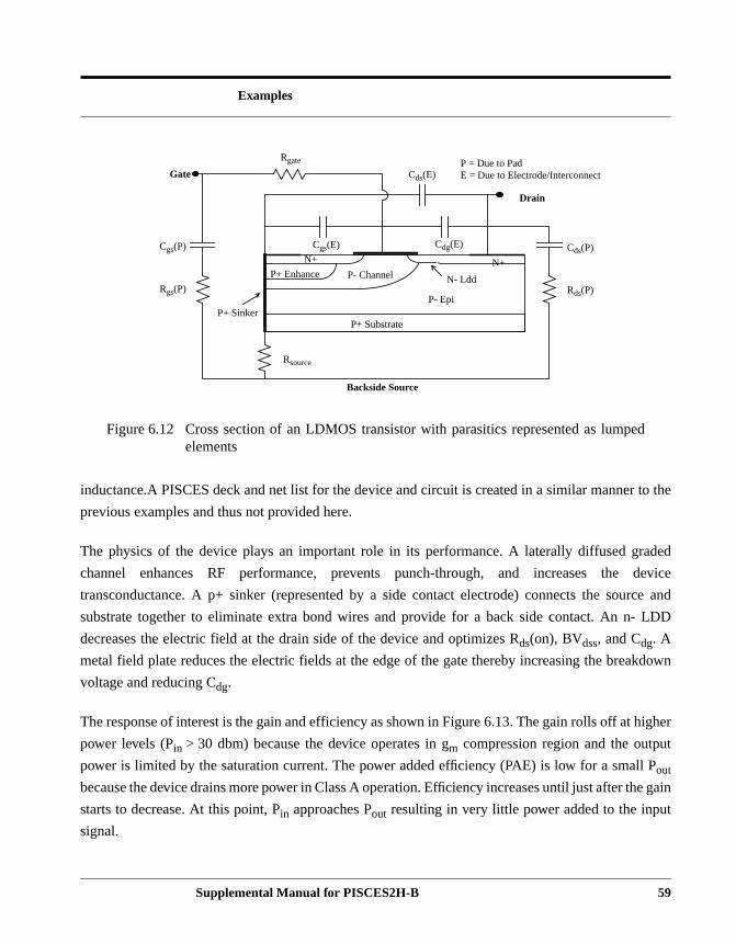
Examples
r to the
raded
device
rce and
- LDD
akdown
higher
t
ll P
he gain
t
d
inductance.A PISCES deck and net list for the device and circuit is created in a similar manne
previous examples and thus not provided here.
The physics of the device plays an important role in its performance. A laterally diffused g
channel enhances RF performance, prevents punch-through, and increases the
transconductance. A p+ sinker (represented by a side contact electrode) connects the sou
substrate together to eliminate extra bond wires and provide for a back side contact. An n
decreases the electric field at the drain side of the device and optimizes Rds(on), BVdss, and Cdg. A
metal field plate reduces the electric fields at the edge of the gate thereby increasing the bre
voltage and reducing Cdg.
The response of interest is the gain and efficiency as shown in Figure 6.13. The gain rolls off at
power levels (Pin > 30 dbm) because the device operates in gm compression region and the outpu
power is limited by the saturation current. The power added efficiency (PAE) is low for a smaout
because the device drains more power in Class A operation. Efficiency increases until just after t
starts to decrease. At this point, Pin approaches Pout resulting in very little power added to the inpu
signal.
Drain
Gate
Backside Source
P+ Sinker
N+P- Channel
P- Epi
N- Ldd
N+
P+ Enhance
P+ Substrate
Cgs(E)
Cds(E)
Cdg(E)
Rsource
Rgate
Cds(P)
Rds(P)
Cgs(P)
Rgs(P)
P = Due to PadE = Due to Electrode/Interconnect
Figure 6.12 Cross section of an LDMOS transistor with parasitics represented as lumpeelements
Supplemental Manual for PISCES2H-B 59
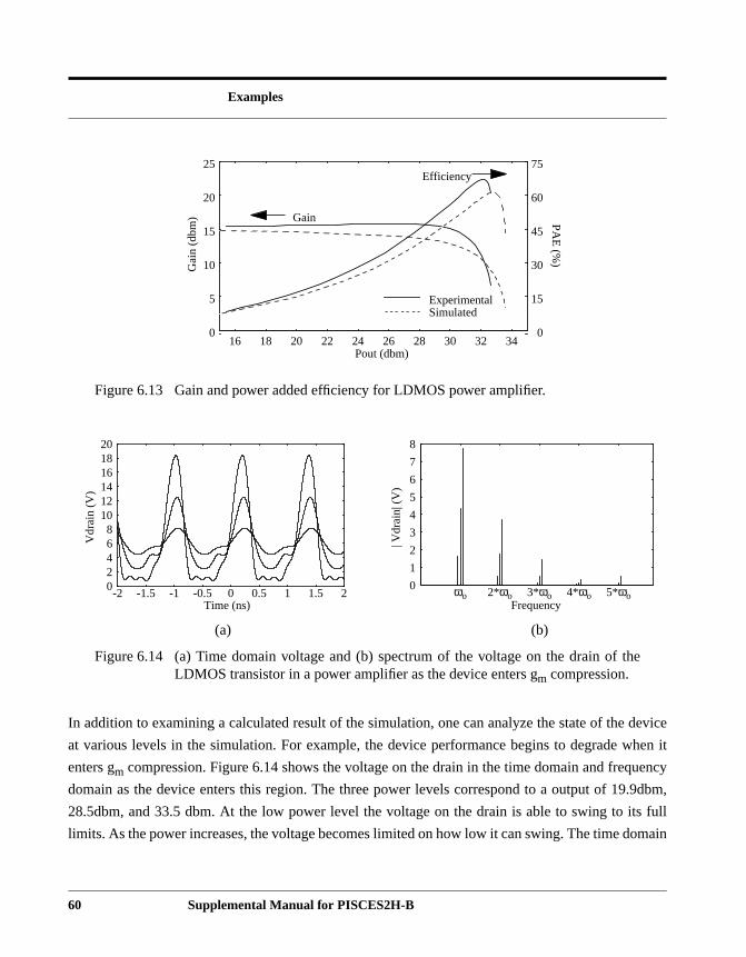
Examples
device
hen it
uency
.9dbm,
ts full
omain
e
In addition to examining a calculated result of the simulation, one can analyze the state of the
at various levels in the simulation. For example, the device performance begins to degrade w
enters gm compression. Figure 6.14 shows the voltage on the drain in the time domain and freq
domain as the device enters this region. The three power levels correspond to a output of 19
28.5dbm, and 33.5 dbm. At the low power level the voltage on the drain is able to swing to i
limits. As the power increases, the voltage becomes limited on how low it can swing. The time d
0
15
30
45
60
75
16 18 20 22 24 26 28 30 32 340
5
10
15
20
25
ExperimentalSimulated
Efficiency
Gain
Pout (dbm)
PA
E (%
)Gai
n (d
bm)
Figure 6.13 Gain and power added efficiency for LDMOS power amplifier.
02468
101214161820
-2 -1.5 -1 -0.5 0 0.5 1 1.5 2
Vdr
ain
(V)
Time (ns)
0
1
2
3
4
5
6
7
8
ωo 2*ωo 3*ωo 4*ωo 5*ωoFrequency
| Vdr
ain|
(V
)
Figure 6.14 (a) Time domain voltage and (b) spectrum of the voltage on the drain of thLDMOS transistor in a power amplifier as the device enters gm compression.
(a) (b)
60 Supplemental Manual for PISCES2H-B
Examples
signal
at the
ysical
s the
ximum
plot and the frequency plot reflect that change by two different mechanisms. The time domain
flattens out when it swings low. The spectrum reflects this effect with the addition of harmonics
higher frequencies.
This example clearly shows the power of the harmonic balance device simulation. The ph
characteristics of an advance technology impact simulation significantly. Hence, this tool allow
design engineer to analyze and optimize a robust devices in order to achieve the ma
performance.
Supplemental Manual for PISCES2H-B 61

Examples
62 Supplemental Manual for PISCES2H-B
References
ing at
telli.2.
Ac-
nsac-
sient985.
is ofSI-
OSisco,
nol-A:
References
[1] Troyanovsky, Boris.Frequency Domain Algorithms for Simulating Large Signal DistortionSemiconductor Devices. Dissertation Submitted to the Department of Electrical EngineerinStanford University. November 1997.
[2] Johnson, B., T. Quarles, A. R. Newton, D.O Pederson, and A. Sangiovanni- VincenSPICE3 Version 3f User's Manual. Berkeley: Regents of the University of California, 199
[3] McCalla, William J. Fundamentals of Computer-Aided Circuit Simulation. Boston: Kluwer ademic Publishers, 1993.
[4] Laux, S. E. “Techniques for small-signal analysis of semiconductor devices.” IEEE Trations on Electronic Devices, Vol. ED-32, No. 10, pp. 22028-2037, 1985.
[5] Bank, R., W. M. Coughran, W. Fichtner, E. H. Grosse, D. J. Rose, and R. K. Smith, “Transimulation of silicon devices and circuits.” IEEE Transactions on Electron Devices, Oct. 1pp. 1992-2007.
[6] B. Troyanovsky, F. Rotella, Z. Yu, R. Dutton, and J. Sato-Iwanga. “Large Signal AnalysRF/Microwave Devices with Parasitics Using Harmonic Balance Device Simulation.” SAMI. Fukuoka, Japan: Nov. 1996.
[7] Gordon Ma, Wayne Burger, Chris Dragon, and Todd Gillenwater. “High Efficiency LDMPower FET for Low Voltage Wireless Communications.” Proceedings of IEDM. San FrancCA: December 1996.
[8] Alan Wood, Chris Dragon, and Wayne Burger. “High Performance Silicon LDMOS Techogy for 2GHz RF Power Amplifier Applications.” Proceeding of IEDM. San Francisco, CDecember 1996.
Supplemental Manual for PISCES2H-B 63

References
Supplemental Manual for PISCES2H-B 64