Embed Size (px)
Citation preview

Superconducting Niobium RF Cavities
Designed to Attain High Surface Electric Fields
D.L. Moffat, T. Flynn, J. Kirchgessner, H. Padamsee, D. Rubin, J. Sears, Q. ~ h u *
Laboratory of Nuclear Studies, Cornell University, Ithaca, NY 14853-5001
Abstract
Two cavities have been designed to study the behavior of superconducting niobium cavities
at high surface electric fields. The first, designated Mark I, is a completely welded cavity
which has been tested several times. After some initial difficulties with low Q. values we 9 were able to reach a Q. of -3x10 at 1.5K at low fields. Upon raising the RF power'we
encountered several multipacting barriers that successfully processed away. Ultimately we
were able to apply all of the available RF power (20 watts) to reach a surface electric field
of 145 MV/m and a corresponding magnetic field of 1345 gauss. Emission was observed
but we are uncertain of its source. The second cavity, designated Mark 11, has been
designed with a removable baseplate which is attached to the cavity with an indium seal. 9 This cavity has achieved a Q, of -9x10 at 1.5K at low fields. The multipacting barriers in
this cavity occur at relatively low fields, -10 MV/m peak surface electric field, and do not
yield to processing. Ultimately thermal breakdown occurs. The cause of this strong
multipacting is under investigation.
* Work supported by the National Science Foundation with supplemental funding from the
US- Japan agreement
Proceedings of the Fourth Workshop on RF Superconductivity, KEK, Tsukuba, Japan
SRF89G03

Int reduction
Among the most basic questions pertaining to the high field capability of superconducting
niobium cavities is whether the niobium surface, under any condition, will tolerate the
surface electric fields required for its incorporation into a particle accelerator. DC fields as
high as 200 MV/m have been achieved over surfaces as large as a square centimeter [l].
The highest RF surface field ever achieved, however, had been only 70 MV/m [2 ] . The
typical niobium accelerating cavity design requires that a cavity operating near the
theoretical magnetic field limit of 2000 gauss be capable of supporting a surface electric
field of -100 MV/m.
Heat treated 1500 MHz single cell accelerating cavities in our laboratory now frequently
reach peak surface fields of 40 - 53 MV/m (the peak field occurs where the beam tubes join
the cavity, i.e. the irises) [3]. Evidence to date suggests that under many circumstances
emitters are extrinsic to the niobium walls of the cavity. The probability of encountering
such emitters in a certain region of a cavity is proportional to the surface area of that region.
The irises of an accelerating cavity constitute a relatively large area and, therefore, there is a
high probability that an emitter will be found there. Because this is the region of the
highest electric fields, an emitter here will limit the application of higher fields elsewhere.
Thus, by limiting the area of the high field region of a cavity we may be able to determine
the intrinsic capabilities of niobium. Conversely, we may be able to create or place an
emitter in a controlled manner at a position where it will dominate the performance of the
cavity. In this way more information about the nature of actual emitters may be obtained
and effective processing techniques developed.
These ideas have led us to develop two new cavities. A standard niobium S-band
accelerating cavity half-cell is closed off near the equator with a niobium plate. In the Mark
I cavity this plate is welded to the half-cell. The baseplate in the Mark I1 cavity is attached
with an indium 0-ring. The modes studied are non-accelerating higher order monopole
modes in which the area exposed to the highest electric fields is very small. In addition, the
fields in this region are 4-6 times higher than anywhere else in the cavity, depending on the
mode. The ratio of peak surface magnetic field to peak surface electric field is also quite
favorable, e.g. at 100 MVlm the peak surface magnetic field is 1000-1200 gauss.
Proceedings of the Fourth Workshop on RF Superconductivity, KEK, Tsukuba, Japan
SRF89G03

The Mark I Design
Calculations and Copper Model Tests
The Mark I cavity design is shown in Figure 1. It was designed around existing S-band
niobium half-cells. The frequency of the TMOIO mode in an accelerating cavity using these
cells is about 2856 MI-Iz. It was known that placing a metallic plate at the equator of an accelerating cavity would create high E fields on the plate in a mode at roughly twice the
frequency of the fundamental [4]. Since any protrusion into the fields would enhance the
fields there, it was decided to put a dimple at the center of the baseplate. The dimensions of
the dimple were determined by deep drawing considerations. The radius of curvature on the
perimeter of the baseplate was set at .25", also for ease of deep drawing. Armed with this
information we used URMEL and URMELT to calculate the mode spectrum of such a
cavity to identify suitable modes (the side port had to be omitted for these calculations) [5].
The beam tube was designed to be a cutoff tube at 2856 GHz but it was clear that it would
not be cutoff at 6 GHz. In fact, the URMEWT calculations demonstrated that the beam tube
was an integral part of the cavity and helped to create the desired field pattern at the dimple.
If the beam tube diameter was reduced to create a cutoff tube, the field pattern was not
completely suitable.
Table 1 shows the results of URMEL and SUPERFISH calculations of the monopole modes
of this cavity [6]. These codes indicate that the field enhancement at the dimple is greatest
in the TMOl l mode, but quite attractive in the TMo2o mode as well. (These mode
classifications pertain to the Mark I cavity and not to the accelerating cavity upon which it
is based. The same modes may be classified differently in an accelerating cavity.) The
mode at 6987 MHz is a resonance of the beam tube. The electric field patterns for the
TMo2o and TMO1 1 modes, as calculated by URMEL, are shown in Figure 2. Figure 3 shows the results of SUPERFISH calculations for the surface electric field as a function of
position along the niobium surface for both modes. The fields have been normalized to 100
MV/m at the dimple to facilitate comparison. For the TMo2o mode, the E field at the
dimple is 4.4 times the next highest field, which occurs on the baseplate, but not in the
vicinity of the dimple. The enhancement factor is 6.5 for the TMOl l mode, with the next
highest field occurring at what would be the iris in an accelerating cavity. For comparison,
in the same cavity, but without the dimple, the enhancement at the center of the baseplate is
only 1.8 in the TMO20 mode, 3.6 in the TMO1 1 mode.
Proceedings of the Fourth Workshop on RF Superconductivity, KEK, Tsukuba, Japan
SRF89G03

Top port for input coupler \
End port for transmitted coupler
FIGURE 1 The Mark I cavity design
Proceedings of the Fourth Workshop on RF Superconductivity, KEK, Tsukuba, Japan
SRF89G03

TABLE 1
Mark I Monopole Modes
URMEL calculations
Mode
%l0 %20
%l1 Tube
Mode
TMol0
TM020
%l 1
Mode type
TMO10 Dipole
Dipole
Quadrupole
TMo20 Dipole
Quadrupole
TMol l Sextupole
='E01 1 Dipole
Tube
MHz -%U- p $k@pk EpkEnext
2736.89 13620 147.1 9.6 2.2
SUPERFISH calculations MHz %U- ~ p k a EpkEpk EpkEnext
2739.24 14328 145.5 9.0 2.2
MHz
2736.89
398 1.03
4992.83 5362.47
5772.59
6076.17
6479.37
6592.21
6632.60
6704.39
6909.74
6986.61
TABLE 2
Mark I Mode Spectrum
Proceedings of the Fourth Workshop on RF Superconductivity, KEK, Tsukuba, Japan
SRF89G03

FIGURE 2 Electric field patterns of the TM020 and TMO1 modes in the Mark I cavity
Proceedings of the Fourth Workshop on RF Superconductivity, KEK, Tsukuba, Japan
SRF89G03

FIGURE
n Q Q
Q
ID m n a
l- =% r;? -In
E \ >- -Q
Q
-G - U " .c
0 urn
'Z? .W U U c.
"JP ID ID
a Q Q
Q
Z I c m l
3 Surface electric fields of the TMOz0 and TMO1 modes in the Mark I cavity
Proceedings of the Fourth Workshop on RF Superconductivity, KEK, Tsukuba, Japan
SRF89G03

It was noted earlier that the probability of an emitter occurring in a given field region of a
cavity was proportional to the surface area of that region. Figure 4 shows plots of surface
area exposed to a given electric field when the peak surface electric field is 100 MV/m for
the TMo2o and TMOl l modes. The total area exposed to fields within 50% of the 2 2 maximum is only 79 mm in the TMo2o mode, 101 mm in the TMOl 1 mode. This is in
contrast to 10100 mm2 under the same conditions in a 1500 MHz accelerating cavity.
There are a great many other modes in this cavity beside the interesting monopoles. Table
2 gives the complete mode spectrum up to 7 GHz. The geometry factor, G, is the product of
R, the RF surface resistance of the cavity walls, and the cavity Q,. The Q, values given for
4.2 and 1.5K assume the BCS resistance of niobium calculated using the program of
Halbritter [7]. Since actual cavities are always somewhat asymmetric, it can be expected
that all of the dipole, quadrupole and sextupole modes will each be slightly polarized, and
thus be split in frequency. This will result in 12 modes between 5773 and 6987 MHz. The
number of modes in the vicinity of the TMOl 1 mode could make it difficult to identify
during a test. On the other hand, the TM020 mode is relatively free of neighbors.
Bench measurements were made on a copper model of the Mark I cavity. Power was
coupled into the cavity using an antenna in the top port. Because the coupling from the end
port was too weak for accurate measurements, the transmitted coupler was placed on the
base plate of the cavity, approximately halfway between the dimple and the equator. Even
here, 60 dB amplification of the transmitted signal was required. In order to identify the
modes which have two polarizations, holes were drilled at 45" intervals around the equator
and a 1/16" sapphire rod inserted across the diameter of the cavity. The sapphire rod
cleared the dimple by about 3/16". Along the diameter, the sapphire rod affected the
splitting of the dipole, quadrupole and sextupole modes and had little effect on the
monopole modes. On axis, however, the sapphire rod greatly affected the frequencies of the
monopole modes.
When the niobium cavity is tested in liquid helium it is under vacuum. This raises the
additional problem of baseplate deflection due to evacuation of the cavity. This was
simulated in the copper cavity by deflecting the baseplate with a C-clamp. The copper
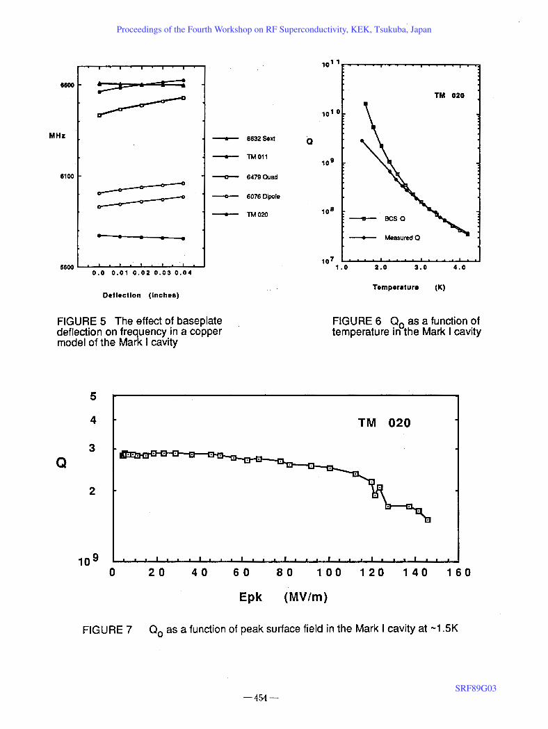
cavity measurements are shown in Figure 5. The TMo2o mode is relatively unaffected by
baseplate deflection. However, baseplate deflection results in the sextupole and TMO1
modes crossing each other at about .020" of deflection. This greatly complicates the
identification of the different modes. URMEL was run for the monopole and sextupole
modes and verified the experimental results. As the deflection increases, the TMO20 mode
Proceedings of the Fourth Workshop on RF Superconductivity, KEK, Tsukuba, Japan
SRF89G03

TM 020 mode
Surface Electric Field (MVIm)
TM 011 mode
0 2 0 . 4 0 6 0 8 0 1 0 0
Surface Electric Field (MVIm)
FIGURE 4 Cavity surface area exposed to a given electric field in the Mark I cavity
Proceedings of the Fourth Workshop on RF Superconductivity, KEK, Tsukuba, Japan
SRF89G03
1 0 ~ ~ ~ . - . . , . . . - , . . . . ~ - .
101 0 ,
l o g - 108 :
: - BCS Q
--t-- Measured Q
Temperature (K) Deflection (inches)
FIGURE 5 The effect of baseplate deflection on frequency in a copper model of the Mark I cavity
FIGURE 6 Q, as a function of temperature in the Mark I cavity
Epk (MVIm)
FIGURE 7 Q, as a function of peak surface field in the Mark I cavity at -1.5K
Proceedings of the Fourth Workshop on RF Superconductivity, KEK, Tsukuba, Japan
SRF89G03

continues to drop in frequency and remains clear of the other modes. The frequency of the
TMOl l mode, as well as that of the neighboring quadrupole mode, increases and eventually
converges on that of the dipole mode at 6910 MHz. At such severe deflections, e.g. around
.16", it becomes extremely difficult to identify the TMOl l mode. Table 3 summarizes the
important results for the TM020 and TMOl 1 modes. These data indicate that the degree of
deflection should be known in order to accurately calculate the electric field at the dimple.
TABLE 3
Bowed Baseplate Calculations
W 2 0 W1 1 Deflection MHz E ~ ~ & . MHz E ~ ~ & .
Niobium Cavity Tests
Two Mark I cavities were made using 1/16" thick niobium with a RRR of -250. All pieces
were joined with electron beam welds. The cavity was attached to the test stand using an
indium 0-ring on the top port, resulting in the baseplate of the cavity being mounted
vertically during testing. The input coupler was an antenna which was inserted into the top
port. This arrangement prevented debris from the sliding contact on the outer conductor of
the coupler from falling directly on the high field dimple. When used, a transmitted coupler
was placed on the end port. After initial evacuation with a separate turbo pump, an ion
pump maintained the vacuum at c 1 0 - ~ torr.
8 In several early tests we encountered difficulties in obtaining Q, values over -5x10 at
1.5K. This limited the surface electric fields to -34 MV/m for our maximum input power
of 20 W. In these tests we used the standard chemical etching surface treatment that is
applied to accelerating cavities. Suspecting that acid treatment of a closed cavity was part
Proceedings of the Fourth Workshop on RF Superconductivity, KEK, Tsukuba, Japan
SRF89G03

of our problem, we heat-treated one cavity for 2.5 hours at 900°C in our UHV furnace.
This choice of temperature was guided by the desire to drive out any hydrogen which may
have been dissolved in the bulk, while at the same time preserving the high initial RRR.
One side-effect of this heat-treatment was to anneal the cavity, allowing the baseplate to
deflect .156" from the nominal flat position when it was evacuated. With this severe
deformation it was impossible to identify the TMOl 1 mode, though the TMO20 mode could
be studied easily.
Subsequently, we discovered and eliminated debris from the test stand and RF feedline
which was another source of our low Q. problems. The cavity was ultrasonically cleaned
upside-down for 2 hours in methanol after which the cavity obtained a Q, of 3.7x10⁷ at
4.2K at 5683 MHz (TMO20). This value was in agreement with the BCS Q. Figure 6
shows that during cooldown the cavity Qo continued to remain at the BCS level until about
2K. The residual Qo was -2.8x10⁹. The BCS Q at 1.5K is -3.6x101°.
Q. VS peak surface electric field for the best test is shown in Figure 7. The downward
curvature of this graph above 100 MV/m is characteristic of field emission. In our 1500
MHz accelerating cavities Q, can drop by more than an order of magnitude due to FE
loading. This suggests that FE loading had not yet become severe. The cavity was finally
able to reach a peak surface electric field of 145 MVIm at the dimple. The corresponding
surface magnetic field was 1345 gauss.
There were several multipacting barriers which were processed quickly on the way to 145
MVIm. Multipacting began at a peak field of -45 MVIm and continued up to -100 MVIm
at which point x-rays were first detected at the top of the dewar. The power was raised until
the x-ray intensity exceeded the limits for safe operation with the existing shielding.
Because the shielding could not be increased during this test, no helium processing was
attempted to increase either Q or E In addition, our high power capability at 6000 MHz pk. is only 20 W and we were very close to that limit as well.
A plot of Pdiss vs shows a deviation from linearity at about 77 MVIm. The data are
shown in Figure 8. When the difference in measured and calculated Pdiss is plotted vs
l/Epk, the typical Fowler-Nordheim plot is obtained (Figure 9). Since the location of the
emitter is unknown the actual field at the emitter is also unknown, precluding an accurate
calculation of the p, the Fowler-Nordheim enhancement factor, of the emitter.
Proceedings of the Fourth Workshop on RF Superconductivity, KEK, Tsukuba, Japan
SRF89G03

Epk (MVIm)
FIGURE 8 Dissipated power in the Mark I cavity at -1.5K
FIGURE 9 Fowler-Nordheim plot from the Mark I cavity at -1.5K
Proceedings of the Fourth Workshop on RF Superconductivity, KEK, Tsukuba, Japan
SRF89G03
In a subsequent test of the same cavity we achieved -80 MVlm with a Q, of 1 . 7 ~ 1 0 ~ . The
peak magnetic surface field was -740 gauss. In this test we were limited by thermal
breakdown.
The Mark II Design
Calculations and Copper Model Tests
The Mark I1 cavity is shown in Figure 10. The coupling ports, beam tube and half-cell are
identical to that of the Mark I design. The design of this cavity was driven by the desire to
be able to remove the high field region of the cavity and examine it in a scanning electron
microscope without introducing artifacts during removal which could be misconstrued as
being emission sites. An equally important criterion was to avoid a design which would
result in a low cavity Q. because of the currents which would inevitably cross the indium
joint. Several schemes were evaluated after which it was decided to make the entire
baseplate removable.
During the design process it was noticed that the TMO1 1 mode had a magnetic field null on
the wall of the half-cell (no current crosses this null, thus it is an ideal location for an
indium joint). By extending the wall of the half-cell, the cavity was lengthened, lowering
the frequency of the TMOl l mode and drawing the field null into the corner of the cavity.
In a perfectly machined cavity this would be sufficient to produce high Qo's. The
additional length required to position the current null in the cavity corner was determined
by URMEL to be .375". A copper model without the choke joint was made to verify these
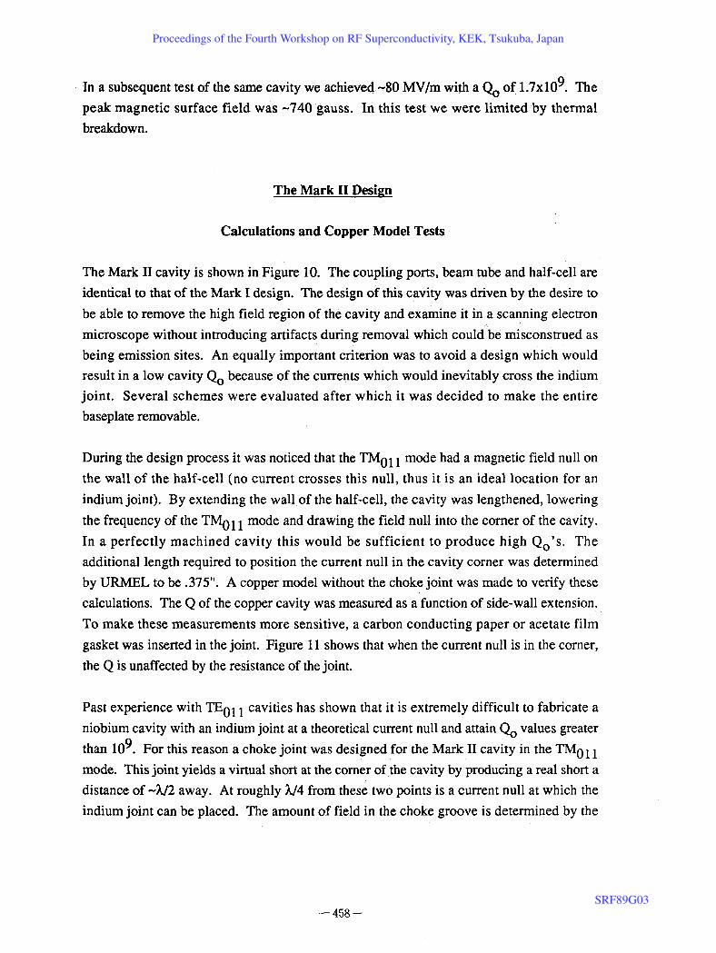
calculations. The Q of the copper cavity was measured as a function of side-wall extension.
To make these measurements more sensitive, a carbon conducting paper or acetate film
gasket was inserted in the joint. Figure 11 shows that when the current null is in the corner,
the Q is unaffected by the resistance of the joint.
Past experience with TEO1 cavities has shown that it is extremely difficult to fabricate a
niobium cavity with an indium joint at a theoretical current null and attain Q, values greater
than log. For this reason a choke joint was designed for the Mark I1 cavity in the TMO1 1
mode. This joint yields a virtual short at the corner of the cavity by producing a real short a
distance of -U2 away. At roughly h14 from these two points is a current null at which the
indium joint can be placed. The amount of field in the choke groove is determined by the
Proceedings of the Fourth Workshop on RF Superconductivity, KEK, Tsukuba, Japan
SRF89G03

rner
v Bolt flanges
FIGURE 10 The Mark II cavity design. The baseplate is joined to the cavity using an indium 0-ring.
Proceedings of the Fourth Workshop on RF Superconductivity, KEK, Tsukuba, Japan
SRF89G03
TM 011 mode 16000
- Paper - Film b
Sidewall extension (inches)
FIGURE 11 Q as a function of extension in a copper model of the Mark II cavity. There was no choke joint on this cavity.
Y) m m
Z (cm1
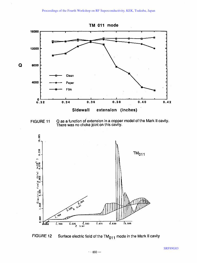
FIGURE 12 Surface electric field of the TMO1 mode in the Mark II cavity
Proceedings of the Fourth Workshop on RF Superconductivity, KEK, Tsukuba, Japan
SRF89G03

FIGURE 13 Electric field pattern of the TMO1 mode in the Mark II cavity
Proceedings of the Fourth Workshop on RF Superconductivity, KEK, Tsukuba, Japan
SRF89G03

field at the cavity corner and the height of the narrow gap joining the groove and cavity.
Ideally the field at the corner of the cavity is zero, so the actual cavity design was a poor
choice for modelling the behavior of the choke joint. To design the choke joint a coaxial
cavity with the same OD as the Mark I1 cavity was used as the host. The length of the
coaxial cavity was such that the frequency of the fundamental mode was the same as the
TMOl l mode in the Mark I1 cavity. In this mode, the magnetic field is at a maximum at the
corners of the coaxial cavity. Using URMEL extensively, the choke joint was tuned to give
a current null at the position of the indium joint without perturbing the resonant frequency
of the host cavity. A copper model verified the calculations. This joint design was then
added to the rest of the Mark 11 cavity.
The surface electric field for the TMOl l mode is plotted in Figure 12. The electric field
pattern of this mode is shown in Figure 13. It should be noted that in addition to the
magnetic field null in the cavity corner, there is also a null in the electric field at the corner
of the cavity. The important results from URMEL calculations for the monopole modes of
the Mark I1 cavity are given in Table 4.
Mark I1 Monopole Modes
URMEL calculations
Mode MHz &U- E ~ ~ & %kEpk
='%l0 2747.44 13986 136.0 8.72
%20 5620.41 16906 121.1 15.1
='MO1 l 6186.81 17598 248.6 10.4 Tube 6931.14
M V I ~ I ~ J GJMVIm
The complete mode spectrum for the Mark 11 cavity is given in Table 5. These results were
also calculated using URMEL. It should also be noted that the input data used for these
calculations included the choke joint.
Proceedings of the Fourth Workshop on RF Superconductivity, KEK, Tsukuba, Japan
SRF89G03

TABLE 5
Mark I1 Mode Spectrum
Mode type
Monopole
Dipole
Quadrupole
%l0 Sextuple Dipole
Dipole
Quadrupole
%20 Dipole
Quadrupole
TMo l l Sextupole Dipole
Tube
Niobium Cavity Tests
The cavity was first tested with a flat baseplate which was 118" in thickness in order to
minimize any deflection of the baseplate due to evacuation. This ensured that the frequency
of the 1 mode did not stray from the frequency at which the choke joint was designed for maximum effectiveness. The Q, at 4.2K was -3x10⁷ (in agreement with the BCS Q)
and the frequency of the TMOl l mode was 6294 MHz, 108 MHz above the design
frequency. The Q, at 1.5K at low power was 6 .4~10~. This is one of the highest Q's ever
acheived in a cavity with an indium joint integral to the cavity. Upon raising the power,
multipacting immediately followed by thermal breakdown occurred at a peak surface
electric field of only 6 MVIm. This barrier could not be processed by either RF or He
processing.
Proceedings of the Fourth Workshop on RF Superconductivity, KEK, Tsukuba, Japan
SRF89G03

Two other modes had Q, values in excess o f . 1 0 ~ . The TMOZO mode exhibited
multipacting and breakdown, but at a field of -.6 MVIm. The Q of the beam tube mode was 1 . 6 ~ 1 0 ~ . It is interesting to note that three of the four measurable modes were
monopoles. This would imply that the choke joint selectively damped the higher order
modes.
A dimpled baseplate was tested next. This plate was 1/16" thick to allow for the drawing of
the dimple. To prevent its deflection upon evacuation a brace was welded onto the back.
At low power the Q, was 8.8xlo9 at 1.5K. The peak surface electric field at this power
level was 7.9 MVIm. Unfortunately, upon raising the power 1 dB multipacting and thermal
breakdown occurred. In an attempt to process through this barrier the input coupler was
inserted quite far into the cavity with the intent of achieving unity coupling in the
breakdown state. The power was then raised and processing was observed. The coupler
was then backed out and a field of 18 MVIm was attained, but the low power Q. had
dropped to -3x10⁹. This sequence was repeated until no further processing was observed.
The ultimate field reached was 29 MV/m and was limited by multipacting-induced
breakdown.
The source of the multipacting barriers is now under investigation. It has been shown that
the choke joint itself is not responsible. The corner of the cavity at the opening of the choke
joint, however, appears to be a likely candidate for two-point multipacting.
Summary
Using a specially designed cavity we have been able to establish a record surface RF
electric field for niobium of 145 MVIm. The corresponding surface RF magnetic field was
1345 gauss. The test in which these records were established did not indicate what the
upper limits to the performance of niobium were, leaving this question unanswered.
Testing of the Mark I1 cavity is well underway. We have shown that it is possible to 9 achieve Qo's in the high 10 'S with an indium joint. The cavity suffers from heavy
multipacting, the source of which has not yet been identified. Once this problem is
eliminated emphasis will be placed on understanding the nature of RF field emission and
emitters.
Proceedings of the Fourth Workshop on RF Superconductivity, KEK, Tsukuba, Japan
SRF89G03

References
[l] Niedermann, P., Experiments on Enhanced Field Emission, PhD Thesis, University of Geneva, 1986
[2] Citron, A., Compilation of Experimental Results and Operating Experience, Proceedings of the Workshop on RF Superconductivity, Karlsruhe, FRG, 1980, pg.
3-26
[3] S hu,Q.S ., Gendreau,K., Hartung,W., Kirchgessner,J., Moffat,D., Noer, R., Padamsee,H., Rubin,D., Sears,J., R&D in Promess to Overcome Field Emission in Superconductinn Accelerator Cavities, Proceedings of the 1989 Particle Accelerator
Conference, Chicago, IL
[4] Amato, J., private communication
[5] URMEL and URMELT were written by U. Laustroer, U. van Rienen, and T. Weiland, DESY
[6] SUPERFISH is maintained by the Los Alarnos Computer Code Group
[7] Halbritter,J., Comparison Between Measured and Calculated RF Losses in the Superconducting State, Z. Physik, 238, pg. 466, 1970
Proceedings of the Fourth Workshop on RF Superconductivity, KEK, Tsukuba, Japan
SRF89G03