Embed Size (px)
Citation preview
Santa Clara UniversityScholar Commons
Electrical Engineering Senior Theses Engineering Senior Theses
7-16-2014
Supercapacitor power management moduleMichael BrooksSanta Clara University
Anderson FuSanta Clara University
Brett KehoeSanta Clara University
Follow this and additional works at: https://scholarcommons.scu.edu/elec_senior
Part of the Electrical and Computer Engineering Commons
This Thesis is brought to you for free and open access by the Engineering Senior Theses at Scholar Commons. It has been accepted for inclusion inElectrical Engineering Senior Theses by an authorized administrator of Scholar Commons. For more information, please contact [email protected].
Recommended CitationBrooks, Michael; Fu, Anderson; and Kehoe, Brett, "Supercapacitor power management module" (2014). Electrical Engineering SeniorTheses. 7.https://scholarcommons.scu.edu/elec_senior/7
ii
Supercapacitor Power Management Module
BY
Michael Brooks, Anderson Fu, and Brett Kehoe
DESIGN PROJECT REPORT
Submitted in Partial Fulfillment of the Requirements
For the Degree of Bachelor of Science
in Electrical Engineering
in the School of Engineering of
Santa Clara University, 2014
Santa Clara, California
iii
Table of Contents
Signature Page. . . . . . . . . . . . . . . . . . . . . . . . . . . . . . . . . . . . . . . . . . . . . . . . . . . . . . . . . . . . . .i . .
Title Page. . . . . . . . . . . . . . . . . . . . . . . . . . . . . . . . . . . . . . . . . . . . . . . . . . . . . . . . . . . . . . . . . ii
Table of Contents. . . . . . . . . . . . . . . . . . . . . . . . . . . . . . . . . . . . . . . . . . . . . . . . . . . . . . . . . . iii
Abstract. . . . . . . . . . . . . . . . . . . . . . . . . . . . . . . . . . . . . . . . . . . . . . . . . . . . . . . . . . . . . . . . . . v
Acknowledgements . . . . . . . . . . . . . . . . . . . . . . . . . . . . . . . . . . . . . . . . . . . . . . . . . . . . . . .vi
1 Introduction . . . . . . . . . . . . . . . . . . . . . . . . . . . . . . . . . . . . . . . . . . …………………… 1
1.1 Core Statement . . . . . . . . . . . . . . . . . . . . . . . . . . . . . . . . . . . . . . . . . . …………1
1.2 Supercapacitors and Energy Storage . . . . . . . . . . . . . . . . . . . . . . . . . ………......3
1.3 Design Goal . . . . . . . . . . . . . . . . . . . . . . . . . . . . . . . . . . . . . . . . . . …………… 3
1.4 Design Considerations . . . . . . . . . . . . . . . . . . . . . . . . . . . . . . . . . . . . . . . . . . …4
1.5 Module Overview . . . . . . . . . . . . . . . . . . . . . . . . . . . . . . . . . . . . . . . . . . ……...6
Design of Module
2 Charge Management . . . . . . . . . . . . . . . . . . . . . . . . . . . . . . . . . . . . . . . . . . . . . . . . . . . . 8
2.1 Choosing a Supercapacitor . . . . . . . . . . . . . . . . . . . . . . . . . . . . . . . . . . . . . . . …8
2.2 Safely Charging Supercapacitors. . . . . . . . . . . . . . . . . . . . . . . . . . . . . . . . . . . . . 9
2.3 Voltage Balancing Circuit. . . . . . . . . . . . . . . . . . . . . . . . . . . . . . . . . . . . . . . . . . 10
2.4 Charge Sources . . . . . . . . . . . . . . . . . . . . . . . . . . . . . . . . . . . . . . . . . . . . . . . . . . 11
3 Output Utilization. . . . . . . . . . . . . . . . . . . . . . . . . . . . . . . . . . . . . . . . . . . . . . . . . . . . . . . 13
3.1 Single Ended Primary Inductor Converter. . . . . . . . . . . . . . . . . . . . . . . . . . . …13
3.2 LT3959: Compensated SEPIC Feedback Controller . . . . . . . . . . . . . . . . . . . . . .13
3.3 SEPIC Topology . . . . . . . . . . . . . . . . . . . . . . . . . . . . . . . . . . . . . . . . . . . . . . . . 14
3.4 Calculations for SEPIC Design. . . . . . . . . . . . . . . . . . . . . . . . . . . . . . . . . . . . . .. 14
3.5 LTSPICE SEPIC Simulation. . . . . . . . . . . . . . . . . . . . . . . . . . . . . . . . . . . . . . . ..16
3.6. Aplications . . . . . . . . . . . . . . . . . . . . . . . . . . . . . . . . . . . . . . . . . . . . . . . . . . . . . .17
3.7 Sepic Results. . . . . . . . . . . . . . . . . . . . . . . . . . . . . . . . . . . . . . . . . . . . . . . . . . . . .17
3.8 Boost Converter Topology. . . . . . . . . . . . . . . . . . . . . . . . . . . . . . . . . . . . . . . . . . 17
4 Supercapacitor Module Control . . . . . . . . . . . . . . . . . . . . . . . . . . . . . . . . . . . . . . . . . . . 19
4.1 BQ33100 Control Abilities. . . . . . . . . . . . . . . . . . . . . . . . . . . . . . . . . . . . . . . . . .19
4.1.1 Communicating. . . . . . . . . . . . . . . . . . . . . . . . . . . . . . . . . . . . . . . . . . . 19
4.1.2 Charging . . . . . . . . . . . . . . . . . . . . . . . . . . . . . . . . . . . . . . . . . . . . . . . .19
4.1.3 Balancing . . . . . . . . . . . . . . . . . . . . . . . . . . . . . . . . . . . . . . . . . . . . . . . 19
4.2 Output Regulation Options . . . . . . . . . . . . . . . . . . . . . . . . . . . . . . . . . . . . . . . . .20
4.3 External Circuitry . . . . . . . . . . . . . . . . . . . . . . . . . . . . . . . . . . . . . . . . . . . . . . . . 20
4.3.1 Layout . . . . . . . . . . . . . . . . . . . . . . . . . . . . . . . . . . . . . . . . . . . . . . . . . .20
iv
4.3.2 Considerations . . . . . . . . . . . . . . . . . . . . . . . . . . . . . . . . . . . . . . . . . . . .20
Testing, Analysis and Final Prototypes
5 Testing and Analysis. . . . . . . . . . . . . . . . . . . . . . . . . . . . . . . . . . . . . . . . . . . . . . . . . . . . . . 21
5.1 Charge Management Testing . . . . . . . . . . . . . . . . . . . . . . . . . . . . . . . . . . . . . . . ..21
5.2 Communicating with the BQ33100 . . . . . . . . . . . . . . . . . . . . . . . . . . . . . . . . . . . .21
5.2 Charging a Mobile Phone . . . . . . . . . . . . . . . . . . . . . . . . . . . . . . . . . . . . . . . . . . . 22
6 Prototyping . . . . . . . . . . . . . . . . . . . . . . . . . . . . . . . . . . . . . . . . . . . . . . . . . . . . . . . . . . . . ..24
6.1 Containment and support structure . . . . . . . . . . . . . . . . . . . . . . . . . . . . . . . . . . . .24
6.2 Wiring and connecting components . . . . . . . . . . . . . . . . . . . . . . . . . . . . . . . . . . . 25
6.3 Prototyping Boards . . . . . . . . . . . . . . . . . . . . . . . . . . . . . . . . . . . . . . . . . . . . . . . 25
6.3.1 Wire Routing . . . . . . . . . . . . . . . . . . . . . . . . . . . . . . . . . . . . . . . . . . . . . 25
6.3.2 Soldering . . . . . . . . . . . . . . . . . . . . . . . . . . . . . . . . . . . . . . . . . . . . . . . . .26
6.3.3 IC Chips and Break out Boards. . . . . . . . . . . . . . . . . . . . . . . . . . . . . . . .27
6.4 Cost. . . . . . . . . . . . . . . . . . . . . . . . . . . . . . . . . . . . . . . . . . . . . . . . . . . . . . . . . . . . .28
7 Conclusion . . . . . . . . . . . . . . . . . . . . . . . . . . . . . . . . . . . . . . . . . . . . . . . . . . . . . . . . . . . . . . 29
7.1 Summary . . . . . . . . . . . . . . . . . . . . . . . . . . . . . . . . . . . . . . . . . . . . . . . . . . . . . . . . 29
7.2 Ethical Analysis . . . . . . . . . . . . . . . . . . . . . . . . . . . . . . . . . . . . . . . . . . . . . . . . ….29
7.2.1 Analysis Introduction . . . . . . . . . . . . . . . . . . . . . . . . . . . . . . . . . . . . . . . 29
7.22 Energy Storage Ethical Issues and Stakeholders. . . . . . . . . . . . . . . . . . . 29
7.3 Future Work. . . . . . . . . . . . . . . . . . . . . . . . . . . . . . . . . . . . . . . . . . . . . . . . . . . . . . 32
7.4 Lessons Learned . . . . . . . . . . . . . . . . . . . . . . . . . . . . . . . . . . . . . . . . . . . . . . . . . . 32
Reference Material References . . . . . . . . . . . . . . . . . . . . . . . . . . . . . . . . . . . . . . . . . . . . . . . . . . . . . . . . . . . . . . . . . 34
Appendices
A Bill of Materials
B List of figures
C List of abbreviations and technical terms
D Datasheets and specifications
v
Abstract
The purpose of this senior design project is to create a charge management and output
converting power module incorporating an array of supercapacitors as the energy storage
medium. Conventional energy storage components, such as lithium-ion batteries, use
electrochemical reactions to store and release electrons into a system. These batteries are slow to
charge, highly toxic to the environment and delicate compared too many of the systems they are
used in. Supercapacitors are noticeably more rugged and last hundreds to thousands of times
longer than the average chemical reaction-based batteries we are used to using while capable of
charging in less than half the time. Creating a power module that properly handles the use of
supercapacitors is the main focus of this project. The power circuitry included in this design
compensates for the design complications inherent to using supercapacitors, allowing future
designers to more easily integrate supercapacitors as an energy storage solution into their
designs. The power module is capable of charging three supercapacitors in series to 8.1 volts in
one hour.

vi
Acknowledgements
The authors would like to thank a number of people, whom without this project would
have never been possible: A huge thank you to our project advisor, Dr. Timothy J. Healy. We
would also like to thank Jenpop Allport, President of the Santa Clara IEEE Chapter. We would
also like to thank Yohannes Kahsai (Electrical Engineering Lab manager) and Dr. Mahmudur
Rahman (Senior Design Project Seminar Professor) for opening up various resources of the
school to us for use. Mike and Brett would like to thank their respective employers, Würth
Electronik and Project Renovo in Campbell for giving us the experience, and occasionally the
parts and advice, that helped make this project a reality.
1
1 Introduction
1.1 Core Statement
The focus of this design project is to create a supercapacitor module that has
integrated charge control and output conversion. This module will be easy for future designers to
integrate into their designs while remaining relatively inexpensive, giving supercapacitors a leap
forward in terms of usability in today’s design market.
1.2 Supercapacitors and Energy Storage
Capacitors use the electric field created by the movement of charge to store energy. Due
to the absence of chemicals, capacitors can charge and discharge faster and without degradation
caused by discharging too much or charging too fast. In addition, they can withstand temperature
changes, shocks, and vibrations better than most batteries. The carbon materials used in
supercapacitors are less damaging to the environment when disposed of and require little
maintenance. The equivalent series resistance (ESR) of supercapacitors is extremely low
compared to current battery technology (0.29 mΩ vs. 200 mΩ), reducing the design complication
of self-discharging. Supercapacitors do have drawbacks when compared to batteries such as their
low energy density. The Maxwell supercapacitors used in this module have an energy density of
six Wh/kg and a power density of 5,900 W/kg.
2
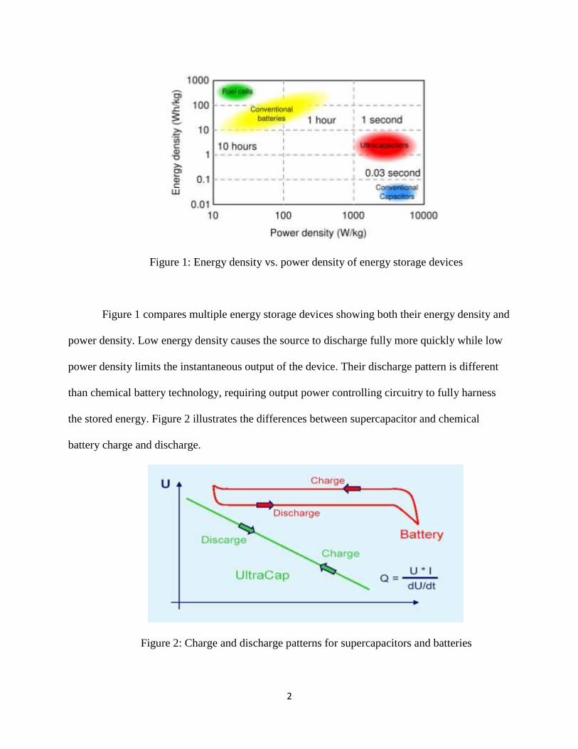
Figure 1: Energy density vs. power density of energy storage devices
Figure 1 compares multiple energy storage devices showing both their energy density and
power density. Low energy density causes the source to discharge fully more quickly while low
power density limits the instantaneous output of the device. Their discharge pattern is different
than chemical battery technology, requiring output power controlling circuitry to fully harness
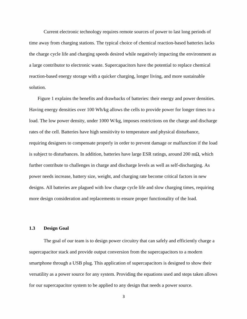
the stored energy. Figure 2 illustrates the differences between supercapacitor and chemical
battery charge and discharge.
Figure 2: Charge and discharge patterns for supercapacitors and batteries
3
Current electronic technology requires remote sources of power to last long periods of
time away from charging stations. The typical choice of chemical reaction-based batteries lacks
the charge cycle life and charging speeds desired while negatively impacting the environment as
a large contributor to electronic waste. Supercapacitors have the potential to replace chemical
reaction-based energy storage with a quicker charging, longer living, and more sustainable
solution.
Figure 1 explains the benefits and drawbacks of batteries: their energy and power densities.
Having energy densities over 100 Wh/kg allows the cells to provide power for longer times to a
load. The low power density, under 1000 W/kg, imposes restrictions on the charge and discharge
rates of the cell. Batteries have high sensitivity to temperature and physical disturbance,
requiring designers to compensate properly in order to prevent damage or malfunction if the load
is subject to disturbances. In addition, batteries have large ESR ratings, around 200 mΩ, which
further contribute to challenges in charge and discharge levels as well as self-discharging. As
power needs increase, battery size, weight, and charging rate become critical factors in new
designs. All batteries are plagued with low charge cycle life and slow charging times, requiring
more design consideration and replacements to ensure proper functionality of the load.
1.3 Design Goal
The goal of our team is to design power circuitry that can safely and efficiently charge a
supercapacitor stack and provide output conversion from the supercapacitors to a modern
smartphone through a USB plug. This application of supercapacitors is designed to show their
versatility as a power source for any system. Providing the equations used and steps taken allows
for our supercapacitor system to be applied to any design that needs a power source.
4
1.4 Design Considerations
As the project began, three foreseeable obstacles became apparent:
Difficulty creating simulations
Circuit construction
Physical construction
Virtual short circuit
In electrical engineering computer simulations are an invaluable asset for the design and
testing of electronic circuits. Early into this project it became clear that we would not be able to
create computer simulations for the charging circuit due to the complexity of the BQ33100
controller IC chip. Hence, the charging circuit had to be constructed and manually tested for
functionality and performance. The LT3959 used for output conversion had a computer
simulation model readily available online which was used to test external component choices for
the SEPIC.
Schematics generally take space for granted and place components in ways that look nice
on paper but may not be feasible on a circuit board, particularly when footprint is an important
constraint. Manipulating the schematic so the connections on the circuit board are in appropriate
places takes a complete knowledge of functionality within the circuit being constructed to ensure
nothing is placed in a position that will create new issues. This was particularly relevant to the
active balancing MOSFETs and resistors, as they had many wires that had to connect to them.
Creating an enclosure for the whole project was an immediately established goal. The
supercapacitors used in the stack are connected by cables between the terminals and are not
meant to be touched by other conducting materials. This meant creating a safe and portable

5
enclosure around the supercapacitors and power circuitry had to account for physical dimensions
as well as electrical characteristics. A smaller enclosure for only the supercapacitors was made
and placed inside a larger case that housed the supercapacitor stack in its enclosure as well as the
power circuitry.
When attempting to charge the supercapacitors from a typical voltage-fed DC power
supply, the short circuit protection circuitry would shut off the power supply. This was caused by
a phenomenon known as a virtual short circuit. Voltage-fed power supplies measure the voltages
at the positive and negative terminals of the supply and compare them, looking for differences in
potential. If no difference is measured the power supply does not provide current to the load.
Uncharged supercapacitors appear as a virtual short to voltage-fed power supplies, not allowing
us to directly charge the supercapacitors by connecting them to voltage-fed power supplies.
As the project progressed there were two unanticipated challenges that impeded progress
towards completion:
Difficulty locating BQ33100 manufacturer
unseal code
Moving from breadboard to
prototype
In order to have control over the full functionality of the BQ33100 chip a special
manufacturer unseal code had to be sent to the chip. Obtaining this code involved numerous
communication attempts with Texas Instruments but in the end we did not receive it in time for
our presentation. Having prepared for this possibility as soon as we discovered we needed the
6
unseal code, we were able to use our backup plan involving only three supercapacitors, the
default setting of the BQ33100.
Moving from the circuit from the breadboard to the prototyping board required
condensing the circuit and soldering all the pieces on. For the small SMD devices small circuit
boards with the proper pad layout and leads connected to each pad were used to make the
assembly process easier. The challenges of circuit design and construction were amplified on the
prototyping board because they require more precision while errors are more difficult to fix.
1.5 Module Overview
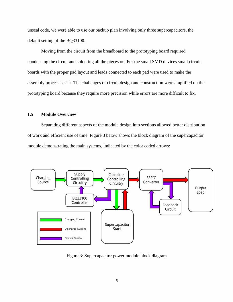
Separating different aspects of the module design into sections allowed better distribution
of work and efficient use of time. Figure 3 below shows the block diagram of the supercapacitor
module demonstrating the main systems, indicated by the color coded arrows:
Figure 3: Supercapacitor power module block diagram

7
The functions of the supercapacitor module are more understandable when divided into the
primary groups of charge control and discharge control. Both groups contain secondary sections
involved with the either controller or feedback circuitry; functions that monitor and alter the
outputs of their respective stages.
8
2 Charge Management
2.1 Choosing a Supercapacitor
Choosing the proper supercapacitor for this project required taking into consideration the
low cell voltage and energy density inherent in supercapacitors. Typical industry load voltages
are 3.3, 5, and 12 volts while the largest supercapacitors have cell voltages of 2.7 volts. Reaching
industry voltage levels would require multiple supercapacitors in series. However,
supercapacitors, like conventional capacitors, lose capacitance when connected in series.
Combined with an already low energy density, the total energy a series supercapacitor stack can
deliver is relatively low, especially considering the size of the supercapacitors. Choosing
supercapacitors with a large capacitance individually was our first method of mitigating these
issues.
The supercapacitors we chose for this design are the Maxwell K2 Series BCAP3000
Supercapacitors. Each supercapacitor has a cell voltage of 2.7 volts and capacitance of 3000
farads. Having the stack voltage exceed the highest of our standard voltage options will benefit
our output converter’s efficiency but lower the effective capacitance. Comparing different series
voltages and capacitances was necessary to determine the best stack voltage to effective
capacitance ratio.
9
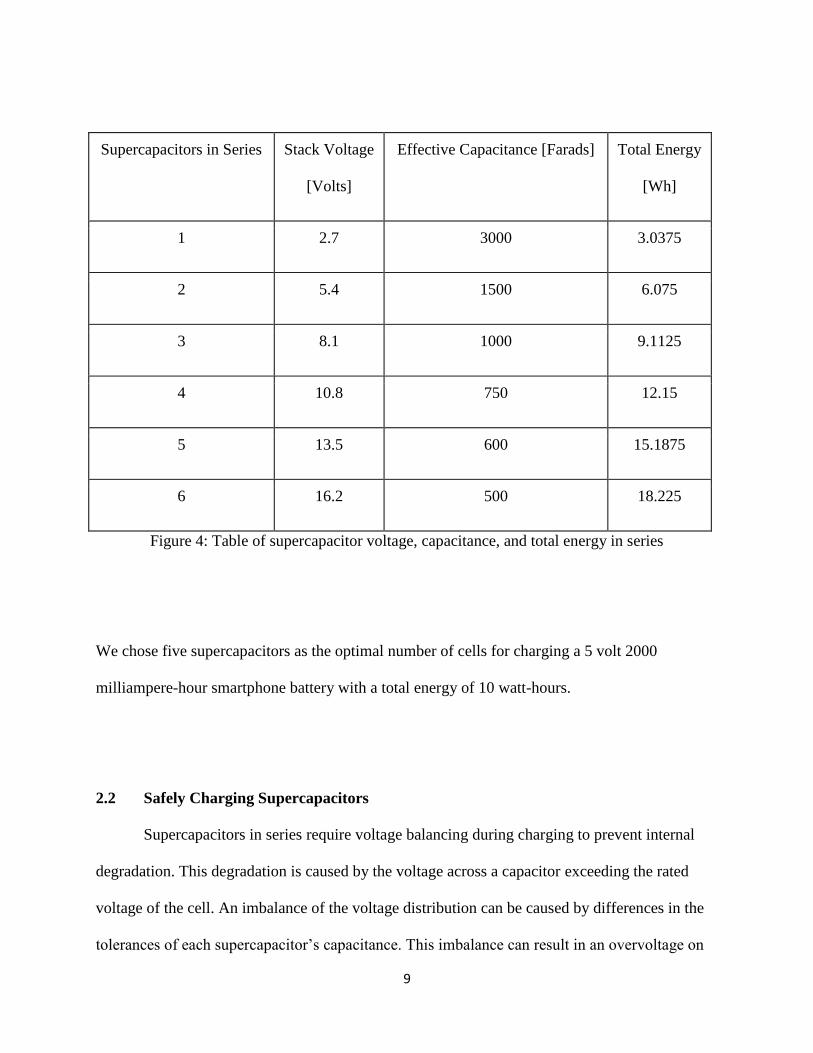
Supercapacitors in Series Stack Voltage
[Volts]
Effective Capacitance [Farads] Total Energy
[Wh]
1 2.7 3000 3.0375
2 5.4 1500 6.075
3 8.1 1000 9.1125
4 10.8 750 12.15
5 13.5 600 15.1875
6 16.2 500 18.225
Figure 4: Table of supercapacitor voltage, capacitance, and total energy in series
We chose five supercapacitors as the optimal number of cells for charging a 5 volt 2000
milliampere-hour smartphone battery with a total energy of 10 watt-hours.
2.2 Safely Charging Supercapacitors
Supercapacitors in series require voltage balancing during charging to prevent internal
degradation. This degradation is caused by the voltage across a capacitor exceeding the rated
voltage of the cell. An imbalance of the voltage distribution can be caused by differences in the
tolerances of each supercapacitor’s capacitance. This imbalance can result in an overvoltage on
10
one or more cells, starting with the cell with the lowest capacitance. Texas Instruments offers a
supercapacitor manager IC called the BQ33100. Our team chose this chip for our project because
it can monitor up to five supercapacitors in series during charging and discharging while
providing measurements related to the supercapacitors and the energy entering or leaving them.
The supercapacitors can be monitored in two different modes, normal mode and stack mode.
Normal mode measures each supercapacitor’s voltage individually while stack mode measures
the total stack voltage.
2.3 Voltage Balancing Circuit
In normal operation mode the Texas Instruments BQ33100 monitors the cell voltage
across each supercapacitor in a series stack and compares each measurement to a preset value.
When a measurement exceeds the preset value, the BQ33100 controls the gate voltage of the
appropriate MOSFET to discharge the supercapacitor until the supercapacitor cell voltage is at
an appropriate level. Figure 5 shows the section of the application reference schematic that
contains the active voltage balancing MOSFETs and resistors. This is the most robust voltage
balancing solution our team could find through our research short of having a microcontroller for
each supercapacitor in the stack.
We had to select power Metal Oxide Semiconductor Field Effect Transistors
(MOSFETs), capacitors, and resistors that could handle the charge current being supplied.
Initially all the components listed in the application reference schematic located on page 50 of
the BQ33100 datasheet were used to test functionality of the charge circuit and supercapacitor
stack. After multiple successful tests, the components along the charge path, designated by the
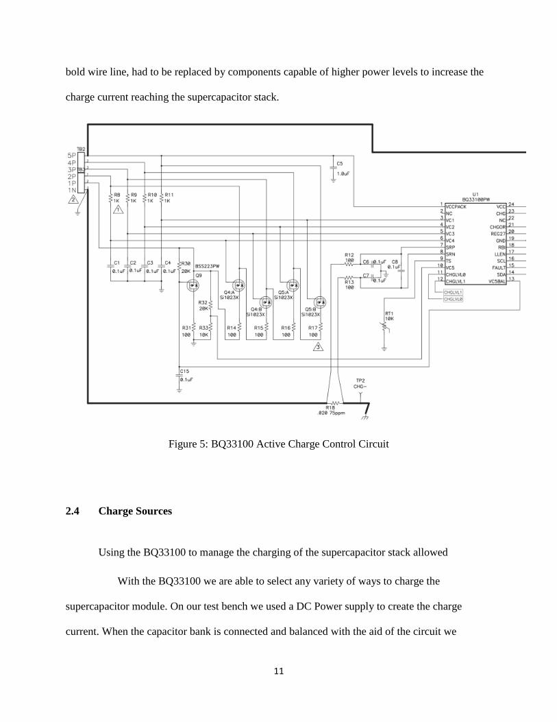
11
bold wire line, had to be replaced by components capable of higher power levels to increase the
charge current reaching the supercapacitor stack.
Figure 5: BQ33100 Active Charge Control Circuit
2.4 Charge Sources
Using the BQ33100 to manage the charging of the supercapacitor stack allowed
With the BQ33100 we are able to select any variety of ways to charge the
supercapacitor module. On our test bench we used a DC Power supply to create the charge
current. When the capacitor bank is connected and balanced with the aid of the circuit we
12
constructed around the BQ33100, it is a simple connection to supply the module with the
necessary power to charge the supercapacitors.
Another option that we considered, but did not find time to investigate, was an AC110
Pigtail wire connected to an ACDC Power converter which could produce a satisfactory voltage
and current for the supercapacitor module. With proper research, we believe an ACDC could be
found that could act as a satisfactory source of power. We also preferred to use a DC Power
supply for a power source as this was much easier to regulate and carefully ratchet up the
allowed voltages and currents we let the module experience. This is however, something to be
considered as an area of future design and testing.
13
3 Output Utilization
3.1 Single-Ended Primary-Inductor Converter
A Single-Ended Primary-Inductor Converter, or SEPIC, is the best converter to properly
deliver power from the supercapacitor stack to an output load. The SEPIC can accept a wide
range of input voltages that can be higher than, lower than, or equal to the desired output voltage.
This converter is ideal to combat the linear decrease of voltage as the supercapacitor stack is
discharged. In a SEPIC there is no DC path between the input and output. This feature is
beneficial for applications that require the output to be disconnected from the input source when
the circuit is in shutdown mode, such as the output power stage for a supercapacitor stack. The
Linear Technology LT 3959 was chosen for the SEPIC feedback control loop due to its low input
voltage once turned on.
3.2 LT3959: Compensated SEPIC Feedback Controller
The LT3959 is a wide input range, current mode, DC/DC controller chip capable of
regulating either positive or negative output voltages from a single feedback pin. Its input range
of 1.6V to 40V with 2.5V start-up voltage is what made the chip an ideal candidate for our
application. These parameters refer to only what the LT3959 chip can handle; not to be confused
with the parameters for which the converter circuit will operate under. Depending on which
topology it is set up in the LT3959 can work as an inverting, boost or SEPIC converter.
14
3.3 SEPIC Topology
Figure 6 shows the LT3959 chip controlling a general SEPIC design topology. The
SEPIC uses two inductors, L1A and L1B, which allow for step-up and step-down performance.
Figure 6: Single-ended primary-inductor converter with LT3959 feedback control
3.4 Calculations for SEPIC Design
Choosing the proper external components for a SEPIC requires understanding the
equations explaining the converter’s operation.
Output voltage selection: The voltage divider created by resistors R1 and R2 in figure 4 is
used to determine the output voltage provided from the converter.
15
Conversion Ratio for Duty cycle: As the supercapacitor power module is used, its voltage
will decrease. To compensate for this loss of input voltage the SEPIC will adjust its duty
cycle to main a constant output voltage.
Maximum Duty Cycle: The minimum input voltage chosen for the SEPIC determines the
maximum duty cycle achievable. The LT3959 compensated SEPIC designed for this project
has a minimum input voltage of 2.5 volts, resulting in a maximum duty cycle of 69%.
( )
( )
Maximum Output Current Capability and Inductor Selection: As shown in the topology
figure, the SEPIC converter contains two inductors which we call L1 and L2. The inductors
can be independent but can also be on the same core since the voltages applied to L1 and L2
are identical throughout the switching cycle.
( )
The current through L1 is the same as the input current. Considering that our proof of
concept was to charge a phone through a micro-USB port, the value of one ampere was
chosen for the output current. Ideally, the output power is equal to the input power which
yields the following equation for maximum inductor currents:
( ) ( ) ( ) ( )
( )
( ) ( )
16
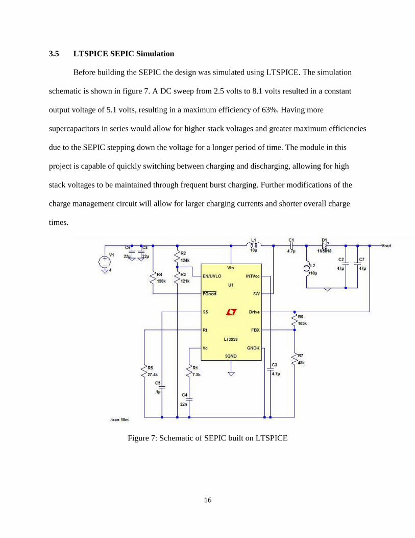
3.5 LTSPICE SEPIC Simulation
Before building the SEPIC the design was simulated using LTSPICE. The simulation
schematic is shown in figure 7. A DC sweep from 2.5 volts to 8.1 volts resulted in a constant
output voltage of 5.1 volts, resulting in a maximum efficiency of 63%. Having more
supercapacitors in series would allow for higher stack voltages and greater maximum efficiencies
due to the SEPIC stepping down the voltage for a longer period of time. The module in this
project is capable of quickly switching between charging and discharging, allowing for high
stack voltages to be maintained through frequent burst charging. Further modifications of the
charge management circuit will allow for larger charging currents and shorter overall charge
times.
Figure 7: Schematic of SEPIC built on LTSPICE
17
3.6 Applications
This output converter is designed to output the appropriate voltage and current to charge a
modern Micro-USB smartphone to demonstrate one way the power of our supercapacitor stack
could be harnessed. Using the equations shown under “Calculation for SEPIC” the user can
change the values to choose the proper components for specific applications. For example, by
changing the values of R2 and R1, the user can change the output voltage as long as it remains
within the limits of the SEPIC topology and L3959.
3.7 SEPIC Results
The physical design of the SEPIC circuit did not function properly when connected to the
supercapacitor stack. Testing the converter with a wall-powered DC power source resulted in
lower output voltages than expected with no output current. The construction of the circuit
provided more soldering challenges than the charge management circuit. Multiple surface mount
components had to be soldered to boards with leads attached, creating multiple fault points in the
circuit if soldered improperly.
3.8 Boost Converter Topology
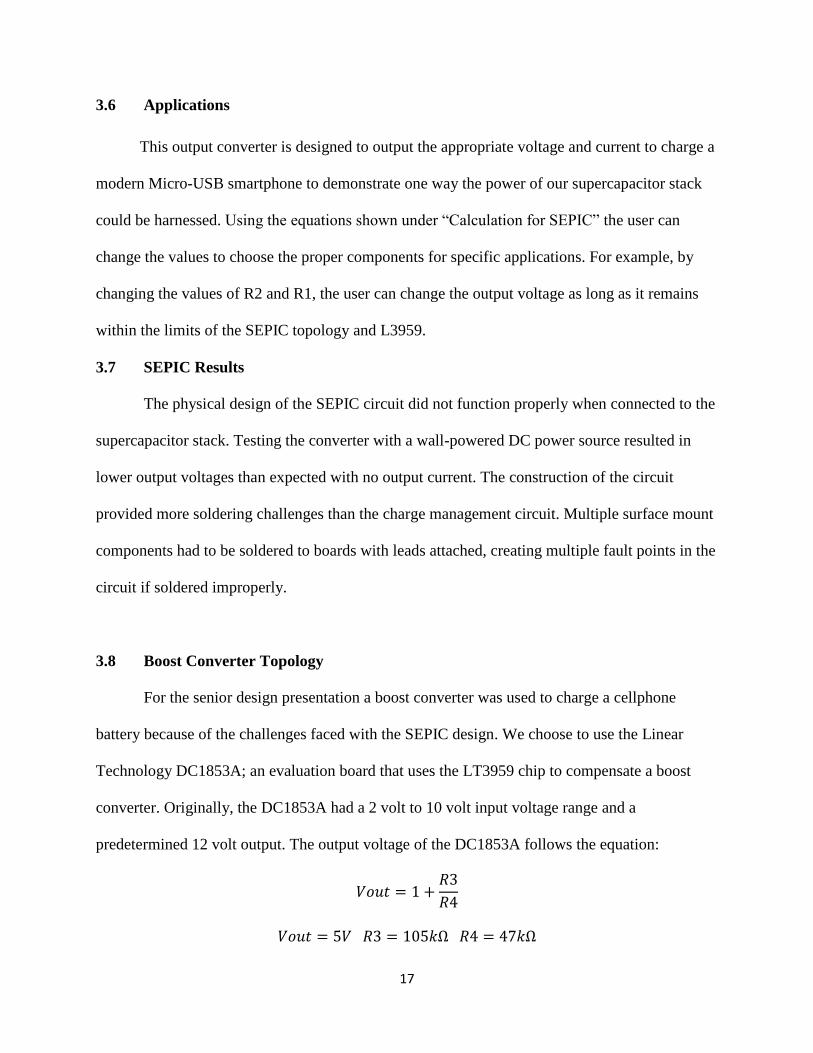
For the senior design presentation a boost converter was used to charge a cellphone
battery because of the challenges faced with the SEPIC design. We choose to use the Linear
Technology DC1853A; an evaluation board that uses the LT3959 chip to compensate a boost
converter. Originally, the DC1853A had a 2 volt to 10 volt input voltage range and a
predetermined 12 volt output. The output voltage of the DC1853A follows the equation:
18
Changing the values of R3 and R4 allows the output voltage to be changed to the
designer’s preference. Due to the challenges restricting the supercapacitor stack to three units,
the total efficiency of the system is lower than the maximum theoretical efficiency noted in the
LT3959 datasheet.
Figure 8: Schematic of altered boost converter (modifications labeled in red)
19
4 Supercapacitor Module Control
4.1 BQ33100 control abilities
The supercapacitor control chip we used allowed us to do a number of things. In turn it
also created challenges and we had to prepare circuits and communicate with IC chips in ways
we hadn’t experienced before.
4.1.1 Communicating
The BQ33100 charge management has control lines that can communicate using an I2C
protocol called SMBus. Using this, we have the ability to read various measurements from the IC
chip and program our various specifications using the commands listed in the chip’s datasheet.
4.1.2 Charging
Even though the supercapacitors were more regulated when being charged with the
BQ33100 control circuit, we still charged our prototype circuit up slowly at first. This proved to
be worthwhile when we found loose solder joints that were not allowing our circuit to function
initially. It was a quick fix, but if full power had been put on the charging path there would have
been a much higher chance that many of the components could have burned out.
4.1.3 Balancing
The MOSFET and resistor array connected to the stack is controlled directly by the
BQ33100 chip, allowing active voltage balancing and leakage current monitoring. Active voltage
balancing allows the supercapacitor stack to be charged safely and quickly, replacing the tedious
task of manually monitoring each supercapacitor’s cell voltage.
20
4.2 Output Regulation Options
Regulating the output voltage and current from the supercapacitor stack depends on the
application. For testing and to prove the concepts of the supercapacitor module, a simple USB
port was chosen to be the power output, and a test phone was charged using its standard charge
cable connected to the module through the USB.
This required a voltage regulator to ensure that the USB terminal was consistently
supplied with the voltage required to charge the phone and the appropriate amount of current for
the battery to safely charge.
4.3 External Circuitry
4.3.1 Layout
Most of the layouts were derived from the datasheets of the main chips used in our
designs. Many of these datasheets contained example diagrams that allowed the team to design
circuits that would achieve our initial goals. The layout of various components dictated the
performance and abilities of the supercapacitor module.
4.3.2 Considerations
Multiple PCBs to create a module allows for a number of advantages but also created
challenges. We would have to house the module in a larger case to accommodate the control
circuitry. We also intended to keep the supercapacitors isolated from the circuitry in order to
prevent either from damaging the other.
21
5 Testing and Analysis
5.1 Charge Management Testing
Initial charge testing began before the BQ33100 circuit was completed. First we
attempted connecting the stack directly to a 12 volt voltage driven power supply. This power
supply would not charge the supercapacitors if they were fully discharged as they appear as a
virtual short to the power supply’s short circuit protection monitor, causing no current to flow
and no charge to accumulate inside the supercapacitors. Initially overcoming this problem
involved attaching a charged battery pack to the supercapacitor stack, draining the batteries into
the stack to provide enough voltage to overcome the virtual short. This workaround was
acceptable for a short time until multiple battery cells ruptured from the resulting high currents
when the supercapacitor stack was connected directly to the battery pack.
Once the BQ33100 charging circuit was laid out on the breadboard, proper charging of
the supercapacitor stack was possible. Because we were unable to unseal the factory settings of
the chip we were unable to utilize the capacitors in a stack of our desired amount. The factory
settings were for a stack of three supercapacitors. As Texas Instruments thus far has been
resistant to share these private codes with us, we have been unable to run all of the tests we
wanted.
5.2 Communicating with the BQ33100
Communicating with the BQ33100 was the first stage in charging our supercapacitor
stack. The BQ33100 requires an I2C device to connect as a master to the BQ33100. An Arduino
Uno microcontroller board allowed us to send and receive messages with the BQ33100. The
22
standard Arduino Wire.h library offers I2C functionality and the Arduino Cookbook offered basic
instructions for that library. We found this method to be inefficient and challenging, especially
considering the long commands needed to be given to the BQ33100. Further research located a
custom library developed by a member of the Arduino community designed specifically for I2C
communication. This library offered more succinct commands, shortening instructions from
multiple lines of code down to a single line.
5.3 Charging a mobile phone
For our proof of concept we chose to test our supercapacitor stack using it to charge a mobile phone. By
charging the phone through SEPIC in the output of the stack we can maximize the charge of the
supercapacitors to our advantange. The phone we decided to use was called the “Samsung Smiley” and
we decided to charge it with 5.1 Volts and 1 Ampere.
We chose to use a USB port, as suppose to the micro USB adapter that plugs directly to the
phone, to increase the universality of our charger. With a USB port, you can charge any phone as long as
you have its USB cable and the voltage and current values are compatible. A type A USB port usually has
four pins: voltage high, info 1, info 2, and voltage low. For our purposes we are only using the first and
last pins since we only need to charge the battery and are not transferring any data from the phone. We
connect the voltage high pin to the output voltage of the SEPIC and the voltage low pin is connected to
the ground of the SEPIC. After doing this, one is ready to charge their mobile device. However, we were
not able to get the physical design of the SEPIC to work properly.
We tested the SEPIC using a DC power source our results showed output voltages and
essentially no output current. We believe that this malfunction was caused by possible fault points while
soldering our components—multiple surface mount components that required the use of soldered to
boards with leads attached proved to be bigger challenge than building the charge management circuit.
23
Due to lack of time we were not able to fix this problem. In hindsight, we were warned by one of our
advisors of the many challenges of building our own converter.
For our presentation we used a Boost converter called the DC1853A mainly because it used
the same LT3959 controller chip. As mentioned earlier the DC1853A had a 2-10V input range
with a 12V output initially but was modified to a 5.1V output. This was a very inefficient model
because we could only use our supercapacitor stack at a minimum charge given that it is a “step
up” converter leaving an small allowed input voltage between 2V - 5.1 V. When we plugged our
cellphone into the USB cable we were able to charge the phone with no interference. This test,
though not efficient, served to prove that we could charge a phone using the power module
without damaging it. Due to the failed attempts with the SEPIC we were not able to maximize
the usage of the supercapacitors and to test how long the module could charge the phone for. We
are positive that this problem is by no mean unsolvable and that will not be an obstacle for our
future work.
24
6 Prototyping
We wanted to create a working prototype to validate the simplicity and effectiveness of
our designs. This was some of the most challenging work, but also some of the most enjoyable.
Our work and results are below.
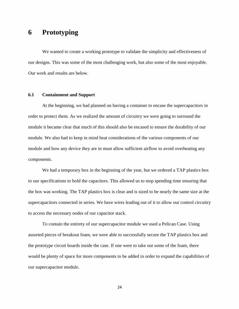
6.1 Containment and Support
At the beginning, we had planned on having a container to encase the supercapacitors in
order to protect them. As we realized the amount of circuitry we were going to surround the
module it became clear that much of this should also be encased to ensure the durability of our
module. We also had to keep in mind heat considerations of the various components of our
module and how any device they are in must allow sufficient airflow to avoid overheating any
components.
We had a temporary box in the beginning of the year, but we ordered a TAP plastics box
to our specifications to hold the capacitors. This allowed us to stop spending time ensuring that
the box was working. The TAP plastics box is clear and is sized to be nearly the same size at the
supercapacitors connected in series. We have wires leading out of it to allow our control circuitry
to access the necessary nodes of our capacitor stack.
To contain the entirety of our supercapacitor module we used a Pelican Case. Using
assorted pieces of breakout foam, we were able to successfully secure the TAP plastics box and
the prototype circuit boards inside the case. If one were to take out some of the foam, there
would be plenty of space for more components to be added in order to expand the capabilities of
our supercapacitor module.
25
We did some research and brainstorming into 3D printing support materials to secure the
supercapacitors and the various boards we want to include within our module. Due to our limited
ability to design 3D parts in mechanical CAD programs, a sleek and ideal case was not viable for
our project. This has potential for future development and designs could be created to fit a
container of any desired size.
6.2 Wiring and Connecting Components
Securely connecting the capacitors was a major consideration from the beginning. We
used ring terminals on the screw posts at the ends of the capacitors to connect them to the charge
circuitry.
6.3 Prototyping Boards
Prototyping boards have the components soldered on and are much slimmer than
breadboards when a circuit is completed. These allow for much more convenient transportation
of the module, but proved to be a considerable challenge to manufacture without any mistakes.
Part of the issue here was the unreliability of certain IC chips when soldered onto breakout
boards.
6.3.1 Wire Routing
In order to correctly map out our prototyping boards we had to keep a lot of important
reference materials nearby. We had to keep the BQ33100 datasheet printout with the control
circuit to ensure we included all necessary components and paths. Before soldering critical
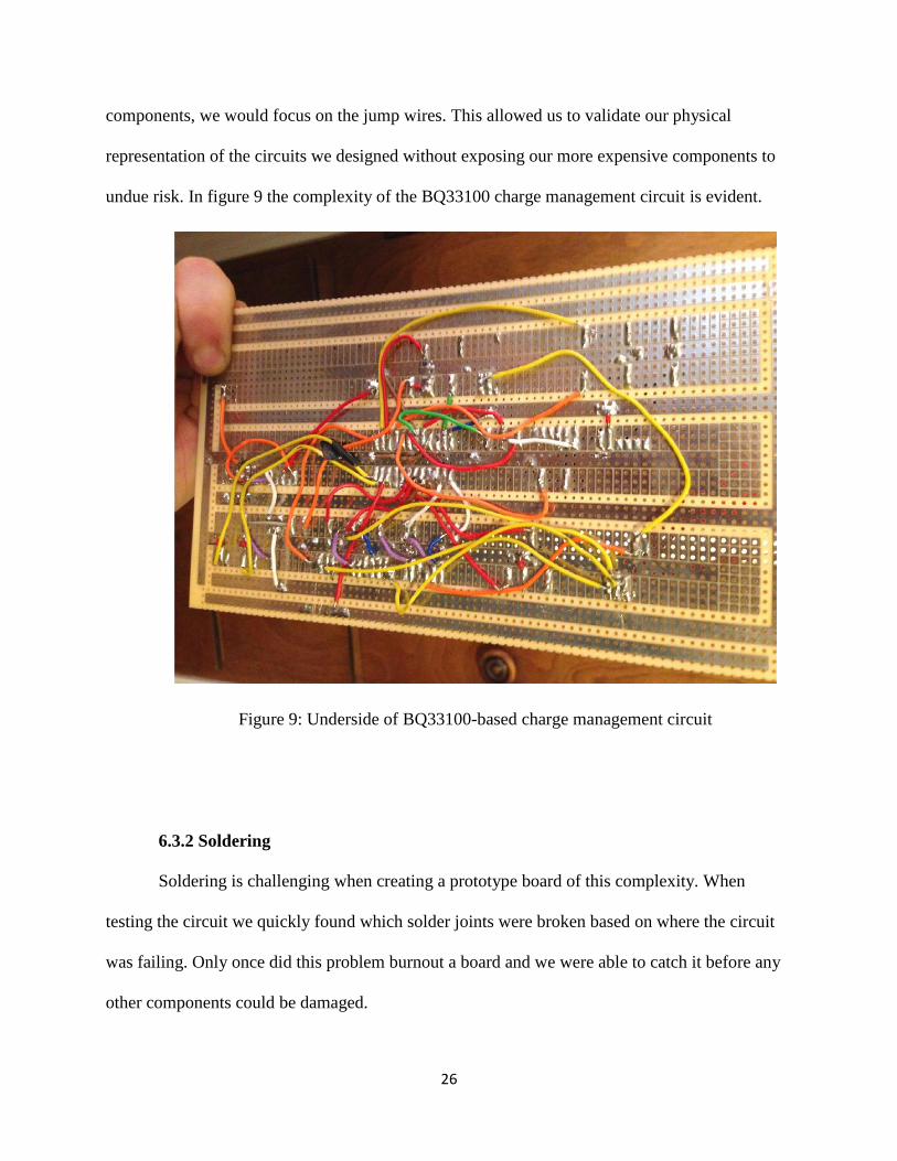
26
components, we would focus on the jump wires. This allowed us to validate our physical
representation of the circuits we designed without exposing our more expensive components to
undue risk. In figure 9 the complexity of the BQ33100 charge management circuit is evident.
Figure 9: Underside of BQ33100-based charge management circuit
6.3.2 Soldering
Soldering is challenging when creating a prototype board of this complexity. When
testing the circuit we quickly found which solder joints were broken based on where the circuit
was failing. Only once did this problem burnout a board and we were able to catch it before any
other components could be damaged.
27
Eventually, we found a method that worked effectively for ensuring secure solder joints
on our boards. We would apply flux to the lead first, and then use the iron to lay solder down on
the lead. This allowed us to prevent dry solder sockets from forming and enabled us to create
solder joints more quickly once the components were inserted in the board.
6.3.3 IC chips and Breakout boards
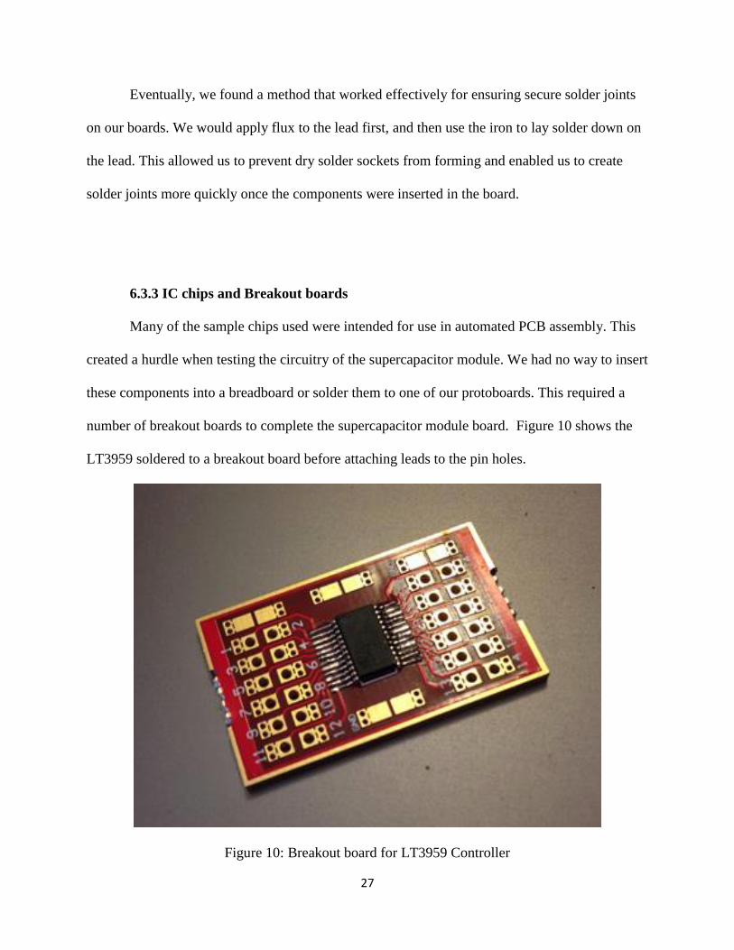
Many of the sample chips used were intended for use in automated PCB assembly. This
created a hurdle when testing the circuitry of the supercapacitor module. We had no way to insert
these components into a breadboard or solder them to one of our protoboards. This required a
number of breakout boards to complete the supercapacitor module board. Figure 10 shows the
LT3959 soldered to a breakout board before attaching leads to the pin holes.
Figure 10: Breakout board for LT3959 Controller

28
6.4 Cost
In its entirety, the cost of this design project accumulates to approximately 635 dollars.
For a more a detailed account of our spending can be seen in the bill of materials located in
Appendix A. when considering mass production, we expect that the cost of fabrication will drop
to 350 dollars. The major expenses of our project include the Maxwell Capacitors, MOSFETS,
IC chip Sockets, and the containers of our module. Upon mass production we would not use the
expensive pelican case and custom made plastic box from Tap plastics. Even if we did use a
custom made container from TAP plastics again, a plastic box would cost fewer than 10 dollars
when bought in bulk. As for the rest of the major components, Mouser Electronics’s website
shows a decrease of at least 30 percent in cost in each of the components with the purchase of
200. As a group we are content with 350 cost of fabrication because it is still competitive with
Maxwell current power module with six supercapacitors priced at 595 dollars.
29
7 Conclusion
7.1 Summary
This project has given our team insight into power circuitry design as well as general
project management skills. Brainstorming together and having different pairs of eyes able to
analyze issues showed us how to play off of each other’s strengths to benefit the team. Whenever
a new obstacle appeared, our team was able to overcome it through determination and research.
Working in a team designing electronics is perfect practice for industry work in a design
position, and has taught us skills that will make us better engineers in the real world.
7.2 Ethical Analysis
7.2.1 Analysis Introduction
An inexpensive and efficient supercapacitor energy management system could
bring supercapacitors to the front of the energy storage market. Understanding how this device
will impact different demographics of people is important to the research and development of an
effective, functional, and safe product. This report will analyze team, design, and social aspects
of the project and explain how to take the ethical concerns of the stakeholders involved in each
aspect into account.
7.2.2 Energy Storage Ethical Issues and Stakeholders
The overarching ethical issue lies in the proper control of the energy being stored
to ensure safe operation both for users and devices. Our project has two main ethical

30
stakeholders: the design engineers creating products with our module and the end users of those
products.
The design engineers will need technical information regarding our module to effectively
and safely integrate it into a product. Our interaction with end users is minimal since our module
will be used to power numerous applications designed by others. This limits our ability to give
important safety information to the end users, making easily comprehendible safety diagrams a
necessity.
Specific ethical situations in the categories of team and organization, project design, and
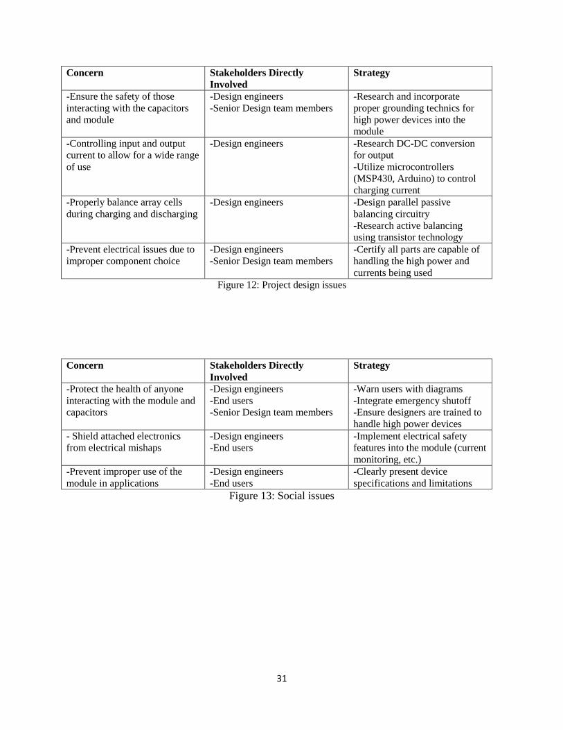
social interaction are cited below in figures 11 through 13, respectively:
Concern Stakeholders Directly
Involved
Strategy
-Ensure team members are
contribute equally
-Senior Design team members -Create and follow Gantt Chart
to divide up responsibilities and
set project goals
-Enforce documentation of
research and resources used
-Senior Design team members -Document resources explaining
their origin and purpose
-Monitor external information to
prevent copyright breaches
-Senior Design team members
-Owners of external work
-Cite used documents (app
notes, design tips, etc.) clearly
explaining what was used
-Cultivate an understanding of
all the processes incorporated in
the project
-Senior Design team members -Document specific tasks each
member performs
-Meet and ensure all members
are at the same level of
comprehension
-Meet Santa Clara University
requirements for the Senior
Design Project
-Senior Design team members
-SCU advisor
-Schedule team meetings with
the advisor to keep all parties
informed and the project on
track
Figure 11: Team and organizational issues
31
Concern Stakeholders Directly
Involved
Strategy
-Ensure the safety of those
interacting with the capacitors
and module
-Design engineers
-Senior Design team members
-Research and incorporate
proper grounding technics for
high power devices into the
module
-Controlling input and output
current to allow for a wide range
of use
-Design engineers -Research DC-DC conversion
for output
-Utilize microcontrollers
(MSP430, Arduino) to control
charging current
-Properly balance array cells
during charging and discharging
-Design engineers -Design parallel passive
balancing circuitry
-Research active balancing
using transistor technology
-Prevent electrical issues due to
improper component choice
-Design engineers
-Senior Design team members
-Certify all parts are capable of
handling the high power and
currents being used
Figure 12: Project design issues
Concern Stakeholders Directly
Involved
Strategy
-Protect the health of anyone
interacting with the module and
capacitors
-Design engineers
-End users
-Senior Design team members
-Warn users with diagrams
-Integrate emergency shutoff
-Ensure designers are trained to
handle high power devices
- Shield attached electronics
from electrical mishaps
-Design engineers
-End users
-Implement electrical safety
features into the module (current
monitoring, etc.)
-Prevent improper use of the
module in applications
-Design engineers
-End users
-Clearly present device
specifications and limitations
Figure 13: Social issues
32
7.3 Future Work
The work we completed this year has nearly infinite options for more experimentation.
With this final report we prepared the research and designs we used to create our supercapacitor
module in the hopes that other electrical engineering students can continue the research and
design experimentation we have started with this project. This would allow others to expand on
the research we’ve done, and cultivate more opportunities for this alternative energy module that
we designed.
Enabling our power module to discharge in different ways is as simple as creating a new
output converter. The numerous options available and different purposes the module could be
modified to work with are enough to create numerous other projects, further expanding the tested
possibilities for supercapacitors as an energy storage medium.
The reason we went to Dr. Healy as an advisor was due to his experience in photovoltaic
systems. Although we did not have the opportunity to use photovoltaics as our charging source
there is huge potential for supercapacitors and photovoltaic systems working in conjunction.
7.4 Lessons Learned
We all learned an incredible amount this year. All of us who came into the project
and quickly found different strengths developed in past classes and work experience. We learned
enough to become mini experts in regards to supercapacitors, but the most meaningful lessons
came through team management, and finding a way to get things done despite the distractions of
work, classes and life as college seniors.
As a team of three we found it difficult to be able to meet all together due to school and
outside obligations. Overcoming this challenge required the use of technology; email and shared
documents were essential to the continuation of work between team members. This solution

33
introduced the problem of keeping team members in sync with the proper files to be worked on.
Downloading files to a computer removes the ability to share updates automatically, requiring
constant communication to ensure team members are not left behind.
We also all developed our ability to teach our peers throughout the project. With each of
our expertise and a number of tasks we all had to do on the project, we were able to teach each
other and all achieve the same level of competence and comprehension. Some of us have had
previous experience with tutoring or coaching, but helping a peer with aspects of electrical
engineering can often be a very different endeavor. In addition to sharing our knowledge within
the team we were able to assist other senior design teams with questions pertaining to energy
storage and supercapacitors.
Our advisors and the administration did a very effective job to the best of their abilities.
Picking a newer technology made it tricky for many of the professors in the electrical
engineering department to give us much support in regards to making our circuitry work at times.
As the project progressed, the authors realized this wasn’t much of an issue, as the advisors were
there more for administrative support and sending students in the right direction to solve
problems on their own.
The presentation itself offered countless lessons when viewing the audience. Certain
judges and viewers were extremely uninterested until going over circuit diagrams, while others
reacted when component and boards were being demonstrated. Even in the short time we were
speaking we improved in our ability to engage the audience. Once comfortable, and beginning to
discuss the more exciting aspects of our project, it became much easier to engage all of the
audience members and spread our enthusiasm for supercapacitors and power circuitry. This was
a lasting lesson when considering future presentations that will take place in our future careers.
34
References
Tecate Group website - Supercapacitor frequently asked questions
Arduino Cookbook by Michael Margolis ISBN-13: 978-1449313876
I2C Library website: http://www.dsscircuits.com/index.php/articles/66-arduino-i2c-
master-library#comment-612
BQ33100 Data sheet: http://www.ti.com/lit/ds/symlink/bq33100.pdf
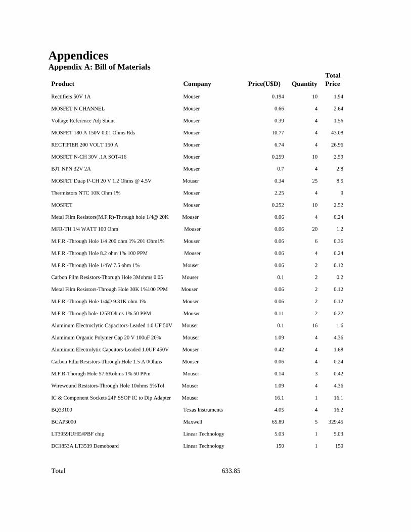
Appendices Appendix A: Bill of Materials
Product Company Price(U$D) Quantity
Total
Price
Rectifiers 50V 1A Mouser 0.194 10 1.94
MOSFET N CHANNEL Mouser 0.66 4 2.64
Voltage Reference Adj Shunt Mouser 0.39 4 1.56
MOSFET 180 A 150V 0.01 Ohms Rds Mouser 10.77 4 43.08
RECTIFIER 200 VOLT 150 A Mouser 6.74 4 26.96
MOSFET N-CH 30V .1A SOT416 Mouser 0.259 10 2.59
BJT NPN 32V 2A Mouser 0.7 4 2.8
MOSFET Duap P-CH 20 V 1.2 Ohms @ 4.5V Mouser 0.34 25 8.5
Thermistors NTC 10K Ohm 1% Mouser 2.25 4 9
MOSFET Mouser 0.252 10 2.52
Metal Film Resistors(M.F.R)-Through hole 1/4@ 20K Mouser 0.06 4 0.24
MFR-TH 1/4 WATT 100 Ohm Mouser 0.06 20 1.2
M.F.R -Through Hole 1/4 200 ohm 1% 201 Ohm1% Mouser 0.06 6 0.36
M.F.R -Through Hole 8.2 ohm 1% 100 PPM Mouser 0.06 4 0.24
M.F.R -Through Hole 1/4W 7.5 ohm 1% Mouser 0.06 2 0.12
Carbon Film Resistors-Thorugh Hole 3Mohms 0.05 Mouser 0.1 2 0.2
Metal Film Resistors-Through Hole 30K 1%100 PPM Mouser 0.06 2 0.12
M.F.R -Through Hole 1/4@ 9.31K ohm 1% Mouser 0.06 2 0.12
M.F.R -Through hole 125KOhms 1% 50 PPM Mouser 0.11 2 0.22
Aluminum Electroclytic Capacitors-Leaded 1.0 UF 50V Mouser 0.1 16 1.6
Aluminum Organic Polymer Cap 20 V 100uF 20% Mouser 1.09 4 4.36
Aluminum Electrolytic Capcitors-Leaded 1.0UF 450V Mouser 0.42 4 1.68
Carbon Film Resistors-Through Hole 1.5 A 0Ohms Mouser 0.06 4 0.24
M.F.R-Thorugh Hole 57.6Kohms 1% 50 PPm Mouser 0.14 3 0.42
Wirewound Resistors-Through Hole 10ohms 5%Tol Mouser 1.09 4 4.36
IC & Component Sockets 24P SSOP IC to Dip Adapter Mouser 16.1 1 16.1
BQ33100 Texas Instruments 4.05 4 16.2
BCAP3000 Maxwell 65.89 5 329.45
LT3959IUHE#PBF chip Linear Technology 5.03 1 5.03
DC1853A LT3539 Demoboard Linear Technology 150 1 150
Total 633.85
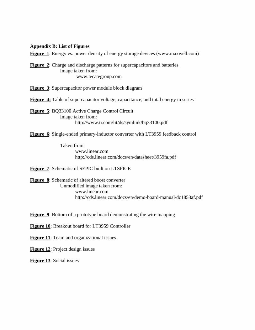
Appendix B: List of Figures Figure 1: Energy vs. power density of energy storage devices (www.maxwell.com)
Figure 2: Charge and discharge patterns for supercapacitors and batteries
Image taken from:
www.tecategroup.com
Figure 3: Supercapacitor power module block diagram
Figure 4: Table of supercapacitor voltage, capacitance, and total energy in series
Figure 5: BQ33100 Active Charge Control Circuit
Image taken from:
http://www.ti.com/lit/ds/symlink/bq33100.pdf
Figure 6: Single-ended primary-inductor converter with LT3959 feedback control
Taken from:
www.linear.com
http://cds.linear.com/docs/en/datasheet/3959fa.pdf
Figure 7: Schematic of SEPIC built on LTSPICE
Figure 8: Schematic of altered boost converter
Unmodified image taken from:
www.linear.com
http://cds.linear.com/docs/en/demo-board-manual/dc1853af.pdf
Figure 9: Bottom of a prototype board demonstrating the wire mapping
Figure 10: Breakout board for LT3959 Controller
Figure 11: Team and organizational issues
Figure 12: Project design issues
Figure 13: Social issues
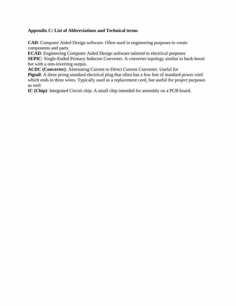
Appendix C: List of Abbreviations and Technical terms
CAD: Computer Aided Design software. Often used in engineering purposes to create
components and parts
ECAD: Engineering Computer Aided Design software tailored to electrical purposes
SEPIC: Single-Ended Primary-Inductor Converter. A converter topology similar to buck-boost
but with a non-inverting output.
ACDC (Converter): Alternating Current to Direct Current Converter. Useful for
Pigtail: A three prong standard electrical plug that often has a few feet of standard power cord
which ends in three wires. Typically used as a replacement cord, but useful for project purposes
as well
IC (Chip): Integrated Circuit chip. A small chip intended for assembly on a PCB board.
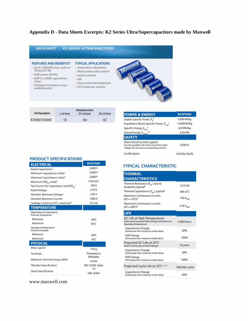
Appendix D - Data Sheets Excerpts: K2 Series Ultra/Supercapacitors made by Maxwell
www.maxwell.com
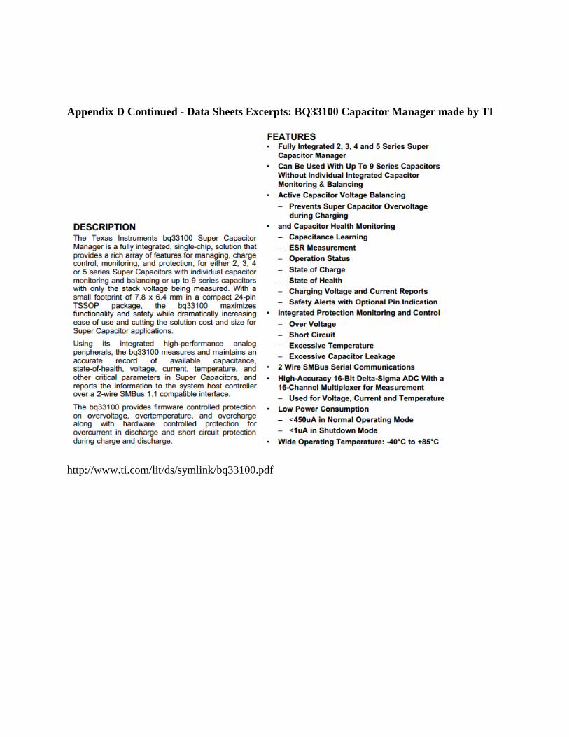
Appendix D Continued - Data Sheets Excerpts: BQ33100 Capacitor Manager made by TI
http://www.ti.com/lit/ds/symlink/bq33100.pdf
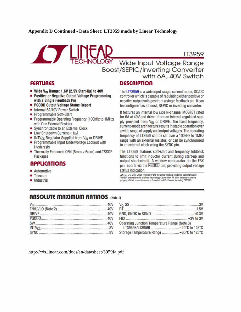
Appendix D Continued - Data Sheet: LT3959 made by Linear Technology
http://cds.linear.com/docs/en/datasheet/3959fa.pdf


![Supercapacitor performance characterization for renewables ... · [5] A. Bostrom, A. von Jouanne, T.K.A. Brekken, A. Yokochi, “Rapid Bidirectional Power Flow of Supercapacitor Energy](https://img.pdfslide.us/doc/110x75/5e31c707c8899b02e05abc22/supercapacitor-performance-characterization-for-renewables-5-a-bostrom-a.jpg)