Embed Size (px)
Citation preview


SUNDAY29 January
REGISTRATION(07:30 - 17:50)
Welcome Address(08:30 - 09:00)
REGISTRATION andWINE & CHEESE
WELCOME RECEPTION(18:30 - 20:30)
Conference Banquet(20:00 - 23:00)
MONDAY30 January
TUESDAY31 JanuaryREGISTRATION(08:00 - 18:00)
WEDNESDAY1 FebruaryREGISTRATION(08:00 - 17:30)
Break & Exhibit Inspection(10:40 - 11:10)
Break & Exhibit Inspection(10:30 - 11:00)
Break & Exhibit Inspection(10:30 - 11:00)
Break & Exhibit Inspection(10:30 - 11:00)
Lunch & Exhibit Inspection(12:30 - 13:30)
Lunch & Exhibit Inspection(12:20 - 13:20)
MEMS 2013Announcement
Lunch & Exhibit Inspection(12:30 - 13:30)
CONFERENCE ADJOURNS(13:20)
Adjourn for the day(17:20)
Adjourn for the day(17:40)
Adjourn for the day(17:50)
THURSDAY2 FebruaryREGISTRATION(08:00 - 13:30)08:00
08:30
09:00
09:30
10:00
10:30
11:00
11:30
12:00
12:30
13:00
13:30
14:00
14:30
15:00
15:30
16:00
16:30
17:00
17:30
18:00
18:30
19:00
19:30
20:00
20:30
21:00
21:30
22:00
PLENARY SPEAKER II(08:30 - 09:10)
PLENARY SPEAKER III(08:30 - 09:10)
POSTER/ORALSESSION IV
(08:30 - 10:30)
POSTER/ORALSESSION I
(13:30 - 15:30)
POSTER/ORALSESSION II
(13:20 - 15:20)
POSTER/ORALSESSION III
(13:30 - 15:30)
PLENARY SPEAKER I(09:00 - 09:40)
SESSION IVFabrication(09:10 - 10:30)
SESSION VIIMedical
Microsystems(09:10 - 10:30)
SESSION IIRF MEMS(11:10 - 12:30)
SESSION VActuators(11:00 - 12:20)
SESSION VIIISensors
(11:00 - 12:20)
SESSION XINano &Materials(12:00 - 13:20)
SESSION VIBio & ChemicalMicrosystems
(15:50 - 17:50)
SESSION IIIPower MEMS
(16:00 - 17:40)
SESSION IOptical MEMS
(09:40 - 10:40)
SESSION XGyroscopes
(11:00 - 12:00)
SESSION IXMicrofluidicComponents& Systems(16:00 - 17:20)
Break & Exhibit Inspection(15:30 - 16:00)
Break & Exhibit Inspection(15:20 - 15:50)
Break & Exhibit Inspection(15:30 - 16:00)

1
The Technical Program consists of three plenary speaker presentations, a general session of contributed papers and 4 poster/oral sessions.
Oral SessionsAll oral sessions will be held in the La Seine Ballroom, Level 0.
Poster/Oral SessionsThe poster/oral format will consist of three (3) scheduled 10 minute, oral presentations which will be presented during each poster session on theirassigned day in front of each poster starting at the designated times below. The remainder of the time should be used for questions & answers. Thechimes will ring five minutes before the start of each presentation. Posters will be on display from Monday at 07:30 through Thursday at 11:00 in the LesClubs de Jazz, Level -1. All poster papers are listed in this program by topic category with their assigned number starting on page 13. Authors will beavailable for questions throughout the entire assigned session.
Guide to Understanding Poster NumberingEach poster is assigned a unique number which clearly indicates when and where the poster is presented. The number of each poster is shown on theleft-hand side before the title. The number (i.e. 132) is the assigned poster board position on the floorplan. See floorplan on page 58.
A typical poster number is shown here is 132-Th
The next character (i.e. Th) indicates the day of the Conference: M = Monday, T = Tuesday, W = Wednesday, Th = Thursday
Page NumberingTo assist you with finding the paper in the Technical Digest, we have provided the page number following each paper title.
SESSION IMonday, 30 January13:30 – 15:30Poster/Oral Presentation 1 – 14:00Poster/Oral Presentation 2 – 14:30Poster/Oral Presentation 3 – 15:00
SESSION IITuesday, 31 January13:20 – 15:20Poster/Oral Presentation 1 – 13:50Poster/Oral Presentation 2 – 14:20Poster/Oral Presentation 3 – 14:40
SESSION IIIWednesday, 1 February13:30 – 15:30Poster/Oral Presentation 1 – 14:00Poster/Oral Presentation 2 – 14:30Poster/Oral Presentation 3 – 15:00
SESSION IVThursday, 2 February08:30 – 10:30Poster/Oral Presentation 1 – 09:00Poster/Oral Presentation 2 – 09:30Poster/Oral Presentation 3 – 10:00
Grand Palais © Paris Tourist Office - Photographer : David Lefranc

2
Sunday - 29 January 2012
Monday - 30 January 2012
18:30 - 20:30 Registration, Wine & Cheese Welcome Reception and Exhibit Inspection
10:40 - 11:10 Break & Exhibit Inspection
08:30 - 09:00 Welcome AddressLionel Buchaillot, IEMN, FRANCEHans Zappe, University of Freiburg, GERMANY
09:00 CHALLENGES AND EMERGING DIRECTIONS IN SPINTRONICS ........................................................................................................................ 1Albert FertUnité Mixte de Physique CNRS and Université Paris-Sud, FRANCE
09:40 A MICRO TRANSLATING LENS UNIT FOR STEREO IMAGING THROUGH SINGLE-IMAGE ENDOSCOPE ............................................................ 3W. Choi1, G. Sigal2, V. Rubtsov2, and C.-J. Kim1
1University of California, Los Angeles, USA and 2Intelligent Optical Systems, Inc. (IOS), USA
A translating lens device is developed to generate stereo images especially for endoscopic applications through a single-objective lens setup. A silicon comb-drive translates aminiature lens across the optical axis in front of an optical circuit to create different viewing angles through a single optical channel. With the added 3D viewing capability, thistechnology aims to enhance the operator’s visual perception and work performance without sacrificing the endoscope’s size.
10:00 A FULLY INTEGRATED OPTOFLUIDIC MICRO-IRIS ........................................................................................................................................... 7P. Müller, R. Feuerstein, and H. ZappeUniversity of Freiburg - IMTEK, GERMANY
We report on a novel type of tunable optofluidic micro-iris composed of a microfluidic chamber filled with two immiscible liquid phases, a highly absorbing aqueous pigmentdispersion and a mixture of transparent silicone oils. The pigment dispersion, which is forced to assume a ring shape using a combination of changes in surface wettability andtopography, defines a circular optical aperture of high contrast. Using integrated electrowetting actuation for tuning the aperture diameter in four discrete steps, a remarkablecompactness of design is achieved.
10:20 POLARIZATION SELECTIVE TUNABLE FILTER VIA TUNING OF FANO RESONANCES IN MEMS SWITCHABLE METAMATERIALS .................. 11W.M. Zhu1, J.H. Teng2, X.H. Zhang2, J.M. Tsai2, Q.Y. Wu2, H. Tanoto2, H.C. Guo2, T. Bourouina3, G.Q. Lo2, D.L. Kwong2, and A.Q. Liu1
1Nanyang Technological University, SINGAPORE, 2Agency for Science, Technology and Research (A*STAR), SINGAPORE, and3Université Paris-Est, FRANCE
We experimentally demonstrated polarization selective tuning of Fano resonance in tunable metamaterial using Microelectromechanical systems (MEMS). The transmissionspectra of TE polarized incidence can be tuned while maintain those of the TM polarized incidence by continuously shifting one trapezoid of the cross-shaped unit cell. Wefabricated an array of 400 _ 400 cross-shaped cells array using silicon deep reactive-ion etching (DRIE) technology. It measures a Fano resonance frequency shift of 37.9% (lowfrequency region) and 25.7% (high frequency region) for TE polarized incidence and only 0.8% for TM polarized incidence. Compared with the previous efforts on tunablemetamaterials, the tunable metamaterial promises unprecedented tunability, such as single to dual band tuning, polarization selective tuning etc.
PLENARY SPEAKER ISession Chairs:
L. Buchaillot, IEMN, FRANCEH. Zappe, University of Freiburg, GERMANY
SESSION I - OPTICAL MEMSSession Chairs:
T. Bourouina, ESIEE, FRANCEH. Urey, Koç University, TURKEY
3
SESSION II - RF MEMSSession Chairs:
T. Kenny, Stanford University, USAG. Piazza, University of Pennsylvania, USA
13:30 - 15:30
POSTER/ORAL - SESSION ISession Chairs:
J. Ducrée, Dublin City University, IRELANDD. Young, University of Utah, USA
11:10 AN INTEGRATED RF MEMS TUNABLE FILTER ................................................................................................................................................ 15Y. Shim, J. Ruan, Z. Wu, and M. Rais-ZadehUniversity of Michigan, USA
This paper reports on a high-performance lumped bandpass filter continuously tuned from 1 GHz to 0.6 GHz using 12 electrostatically actuated MEMS capacitors. To demonstratethe benefits of MEMS technology, a reconfigurable filter array is implemented on a PCB using SMT components and its performance is compared to that of the MEMS filter. Besidesthe advantage in size, the MEMS filter also exhibits lower loss and greater rejection. To become a viable solution for RF applications, other performance specifications of MEMSfilters such as tuning speed and reliability need to be improved.
11:30 A SILICON NITRIDE OPTOMECHANICAL OSCILLATOR WITH ZERO FLICKER NOISE ...................................................................................... 19S. Tallur, S. Sridaran, and S.A. BhaveCornell University, USA
We present an integrated chip-scale Radiation-Pressure driven Opto-Mechanical Oscillator (RP-OMO) in silicon nitride with excellent close-to-carrier phase noise. We illustrate aprocess to micro-fabricate opto-mechanical resonators, waveguides and grating couplers in silicon nitride and demonstrate an RP-OMO operating at 41.947MHz, with phase noiseof -85dBc/Hz at 1kHz offset. The phase noise does not show 1/f^3 or other higher order slopes all the way down to 10Hz offset from carrier.
11:50 A 27 MHZ TEMPERATURE COMPENSATED MEMS OSCILLATOR WITH SUB-PPM INSTABILITY .................................................................... 23R. Tabrizian, M. Pardo, and F. AyaziGeorgia Institute of Technology, USA
This paper reports on the implementation and characterization of a low phase-noise 27 MHz MEMS oscillator with sub-ppm temperature instability based on a high-Q compositebulk acoustic wave resonator. An array of silicon dioxide pillars has been uniformly embedded in the silicon body of a piezoelectrically-transduced resonator to compensate itstemperature coefficient of frequency. Using this technique, overall frequency drift < 90 ppm is achieved over the temperature range of -20°C to 100°C while resonator Q remainsgreater than 7,500 in atmospheric pressure. An electronically compensated oscillator based on these resonators exhibits sub-ppm temperature instability using activeshunt-capacitance cancellation and varactors. Long-term stability measurement has been carried out for both temperature-compensated resonator and oscillator in environmentalchambers to study their long-term frequency and Q stability.
12:10 MICROMACHINED SAPPHIRE GHz LATERAL OVERTONE BULK ACOUSTIC RESONATORS TRANSDUCED BY ALUMINUM NITRIDE ............. 27N.-K. Kuo1, S. Gong1, J. Hartman2, J. Kelliher2, W. Miller2, J. Parke2, S.V. Krishaswamy2, J.D. Adam2, and G. Piazza11Univesity of Pennsylvania, USA and 2Norhrop Grumman Corporation, USA
This work introduces a new class of piezoelectric-transduced bulk acoustic wave resonators formed by a micro-machined c-plane sapphire membrane (~ 750 nm) in the lateralovertone bulk acoustic resonator (LOBAR) configurations. For the first time, thin film sapphire is achieved via a layer transfer process from a single crystal c-plane sapphire wafer.A novel annular geometry exhibits high f_Q of 4.1•E12 Hz and 4.6•E12 Hz at 1 and 2 GHz, respectively with a 9% of transducer to sapphire coverage ratio. The conventionalrectangular LOBAR with coverage ratio of 0.57% exhibits the highest f_Q (1.53·E13 Hz) ever reported for AlN-based suspended resonators.
12:30 - 13:30 Lunch & Exhibit Inspection
15:30 - 16:00 Break & Exhibit Inspection
Monday - 30 January 2012
Notre-Dame, rose window © Paris Tourist Office - Photographer: Amélie Dupont

4
17:40 Adjourn for the Day
SESSION III - Power MEMSSession Chairs:
R. Ghodssi, University of Maryland, USAA. Holmes, Imperial College, UK
16:00 A NOVEL ELECTROMECHANICAL INTERROGATION SCHEME FOR IMPLANTABLE PASSIVE TRANSPONDERS .............................................. 31A. Kim, T. Maleki, and B. ZiaiePurdue University, USA
We report on a novel electromechanical energy scavenging and wireless interrogation scheme using low frequency components of musical vibrations. The device incorporates apiezoelectric cantilever beam that converts the acoustic vibrations into electric power in parallel with a PDMS based inductive pressure sensor. Musical sound wave from aloudspeaker induces vibrations in the piezoelectric cantilever at harmonics, which match its resonant frequency. This, in turn generates a voltage that is rectified and stored in thecapacitor. At non-resonant harmonics, the supply is interrupted, causing the stored charge to be dumped into the sensing LC tank inducing oscillations at its natural frequency,which is picked up externally with a receiver coil.
16:20 A MICROSTRUCTURED CATHODE FOR FUEL CELL WITH SELF-REGULATED O2 BUBBLE CREATION AND CONSUMPTION ........................... 35J.I. Hur and C.-J. KimUniversity of California, Los Angeles, USA
We introduce a monolithic cathode that self-regulates oxygen supply to a fuel cell, complementing the monolithic self-pumping anode previously developed in our lab. Our cathodegenerates oxygen, consumes generated oxygen bubbles, and stops the generation when not consumed, all in a self-regulating fashion. Half-cell tests show reasonable currentoutput, suggesting a complete (full) fuel cell of no moving part in the near future.
16:40 SILICON CARBIDE NANOWIRES AS AN ELECTRODE MATERIAL FOR HIGH TEMPERATURE SUPERCAPACITORS ......................................... 39M. Vincent, M.S. Kim, C. Carraro, and R. MaboudianUniversity of California, Berkeley, USA
We report on the growth of silicon carbide (SiC) nanowires and the evaluation of their performance as electrode material for micro-supercapacitors. Their specific capacitance hasbeen studied as a function of their morphology (size, diameter) and the optimal growth conditions to a capacitance at the level of the state of the art. They exhibit an exceptionalstability, with a lifetime exceeding lead 106 charge/discharge cycles. An excellent thermal stability is expected, opening the way to the fabrication of high temperaturemicro-supercapacitors.
17:00 µL-SCALE MICROBIAL FUEL CELL WITH OPTIMAL POWER GENERATION AND BIOFILM FORMATION ......................................................... 43S. Choi and J. ChaeArizona State University, USA
We report a µL-scale microfluidic Microbial Fuel Cell (MFC) having optimal biofilm formation and minimal oxygen invasion into its anode chamber to generate high power density.We obtained a maximum power density of 95 µW/cm2, the highest value among previously reported µL-scale MFCs and even comparable to that of macro-scale counterparts.
17:20 HIGH EFFICIENT µ-PEMFCS BY INTEGRATING MICRO/NANO SCALED PERFORMANCE IMPROVING COMPONENTS ................................... 47H.-C. Peng1, C.-N. Wang1, Y.-C. Su1, T.-K. Yeh1, and F.-G. Tseng1,2
1National Tsing Hua University, TAIWAN and 2Academia Sinica, TAIWAN
A silicon-based and fully integrated micro proton exchange membrane fuel cell(µ-PEMFC) is introduced in this paper which can carry out high-efficient catalyst utilization andoutstanding cell performance. The design integrates micro/nano-machining technique to enhance reaction surface areas, micro-patterned reaction chamber to create morethree-phase zones and reduce fuel diffusion impedance, and micro-interlocks to solidify interfacial strength and reduce ohmic impedance of a single chip.
Monday - 30 January 2012
Jardin des Tuileries (public garden) © Paris Tourist Office - Photographer : Amélie Dupont

5
Tuesday - 31 January 2012
10:30 - 11:00 Break & Exhibit Inspection
08:30 SEMICONDUCTOR DEVICES INSPIRED BY AND INTEGRATED WITH BIOLOGY .............................................................................................. 51John A. RogersUniversity of Illinois, Urbana-Champaign, USA
Biology is curved and elastic; silicon wafers are not. Semiconductor technologies that can bridge this gap in form and mechanics will create new opportunities in devices thatadopt biologically inspired designs or require intimate integration with the human body. This talk describes ideas for electronics that offer the mechanical properties of a rubberband and illustrates their use in (1) bio-integrated, ‘skin-like’ systems for mapping cardiac and neural electrophysiology, and (2) bio-inspired, ‘eyeball’ cameras for widefield-of-view imaging.
09:10 AN ULTRA-COMPLIANT, SCALABLE NEURAL PROBE WITH MOLDED BIODISSOLVABLE DELIVERY VEHICLE ............................................... 56P.J. Gilgunn1, R. Khilwani1, T.D.Y. Kozai2, D.J. Weber2, X.T. Cui2, G. Erdos1, O.B. Ozdoganlar1, and G.K. Fedder11Carnegie Mellon University, USA and 2University of Pittsburgh, USA
We have developed a fabrication method for the formation of biodissolvable needles that serve as delivery vehicles for ultracompliant neural implants with wire dimensions on theorder of 10 microns width and 3 microns thickness.
09:30 3-D WIRING ACROSS VERTICAL SIDEWALLS OF SI PHOTO CELLS FOR SERIES CONNECTION AND HIGH VOLTAGE GENERATION .............. 60S. Kumagai, T. Yamamoto, H. Kubo, and M. SasakiToyota Technological Institute, JAPAN
This paper first reports 3-D wiring across vertical sidewalls for summing the voltage of Si photo cells based on photolithography. Si photo cells on the buried oxide are isolated byetching the SOI device layer. Wiring using the vertical sidewalls minimizes the shadow region caused by the metal electrode. The techniques of the spray coating of the photoresistand the angled exposure through the absorbent liquid are applied. 100 cells with 100-micrometer spans are connected generating 10.1V.
09:50 FOIL-LEVEL FABRICATION OF INKJET-PRINTED PYROMEMS BALLOON ACTUATORS .................................................................................. 64D.A. de Koninck, F. Molina Lopez, D. Briand, and N.F. de RooijÉcole Polytechnique Fédérale de Lausanne (EPFL), SWITZERLAND
We present the fabrication, modeling and validation of polymeric pyroMEMS balloon actuators compatible with low-cost printing and lamination techniques at the foil level. Thedevice consists of a solid propellant charge deposited within a micro-fabricated cavity covered by a thin PDMS membrane. Fuel combustion generates high-pressure gas, whichinflates the membrane to do work. The resulting devices were not only simpler to fabricate, but consumed less power than similar silicon-based devices.
10:10 A METHOD AND ELECTRICAL MODEL FOR THE ANODIC BONDING OF SOI AND GLASS WAFERS ................................................................ 68E. Tatar, M.M. Torunbalci, S.E. Alper, and T. AkinMiddle East Technical University, TURKEY
This paper provides a method for the anodic bonding of SOI and glass wafers and explains the bonding mechanism with an electrical model, for the first time. SOI-glass anodicbonding can be achieved at voltages as low as 250V similar to Si-glass anodic bonding, and the underlying principles can be understood by modeling the overall system with aseries connected capacitor-resistor network. The proposed model is also successfully adapted to glass-Si-glass anodic bonding.
PLENARY SPEAKER IISession Chairs:
L. Buchaillot, IEMN, FRANCEH. Zappe, University of Freiburg, GERMANY
SESSION IV - FabricationSession Chairs:
S. Lacour, École Polytechnique Fédérale de Lausanne (EPFL), SWITZERLANDL. Lin, University of California, Berkeley, USA

6
12:20 - 13:20 Lunch & Exhibit Inspection
15:20 - 15:50 Break & Exhibit Inspection
13:20 - 15:20
POSTER/ORAL - SESSION IISession Chairs:
S. Franssila, Aalto University, FINLANDS. Sedky, American University in Cairo, EGYPT
Tuesday - 31 January 2012
11:00 SELF-FOLDING CELL ORIGAMI: BATCH PROCESS OF SELF-FOLDING 3D CELL-LADEN MICROSTRUCTURESACTUATED BY CELL TRACTION FORCE ......................................................................................................................................................... 72K. Kuribayashi-Shigetomi, H. Onoe, and S. TakeuchiUniversity of Tokyo, JAPAN
We harness the cell traction force to fabricate cell hinges that induce the rapid origami-like self-folding of flat culture plates into diverse three-dimensional (3D) cell-ladenmicrostructures. In order to gain precise control over the folding angle between the folding plate and substrate, we engineered a flexible joint between the microplates. We achievedmass production of the cell-laden microstructures with precise folding angles.
11:20 MULTIARTICULAR ACTUATOR COMPOSED OF SERIALLY CONNECTED MICROPISTONS FOR WEARABLE ACTUATOR ................................. 76T. Obara and S. KonishiRitsumeikan University, JAPAN
11:40 CONTINUOUSLY LATCHABLE SHUTTLE USING CARBON NANOTUBES ON SIDEWALL SURFACES ................................................................. 80Y. Eun, J. Choi, H. Na, D.-H. Baek, M.-O. Kim, J.-I. Lee, and J. KimYonsei University, SOUTH KOREA
We demonstrated a novel usage of self-adjusted, vertically aligned carbon nanotube (CNT) arrays integrated on the sidewalls as latching components. The CNT array-basedlatching mechanism showed stable latching at multiple latching positions, together with reversible and bidirectional latching capabilities.
12:00 HIGH-PERFORMANCE MEMS RELAY USING A STACKED-ELECTRODE STRUCTURE AND A LEVERING ANDTORSIONAL SPRING FOR POWER APPLICATIONS ......................................................................................................................................... 84Y.-H. Song, C.-H. Han, M.-W. Kim, J.O. Lee, and J.-B. YoonKorea Advanced Institute of Science and Technology (KAIST), SOUTH KOREA
We suggest, fabricate, and demonstrate an electrostatically-actuated MEMS relay, featuring extremely low contact resistance, high stand-off voltage and relay resurrection. It isbased on a unique stacked-electrode structure for very low contact resistance and a levering and torsional spring for enhancing a stand-off voltage (maximum drain voltage towithstand in the off-state) and contact endurance.
SESSION V - ActuatorsSession Chairs:
C.J. Kim, University of Los Angeles, USAS. Takeuchi, University of Tokyo, JAPAN
Montmartre © Paris Tourist Office - Photographer : Amélie Dupont
7
15:50 FEMTOMOLAR SENSITIVITY DNA PHOTONIC CRYSTAL NANOWIRE ARRAY ULTRASONIC MASS SENSOR ................................................... 88Y. Lu, S. Peng, D. Luo, and A. LalCornell University, USA
Here, we present the first-ever nanomechanical mass-sensing resonator with ordered vertical nanowire (NW) arrays on top of a Si/SiO2 bilayer thin membrane acting as a photoniccrystal. The device has a very high surface area-to-volume ratio 10^8 m-1, enabling DNA sensing of femtomolar concentration. For mass-detection-based nanomechanicalbio-sensor, there are two important metrics. The first metric is the minimum detectable mass, which requires a resonator to be as light as possible while maintaining high qualityfactor. The second metric is the minimum detectable mass per area, which requires maximizing sensor surface area, to bind as many detectable bio-molecules as possible.Biosensing at low concentrations, requires not only low minimum detectable mass, but also a large device surface area for molecules to bind to.
16:10 PNEUMATICALLY ACTUATED SPHEROID CULTURING LAB-ON-A-CHIP FOR COMBINATORIAL ANALYSIS OF EMBRYONIC BODY ................ 92T. Nishijima1, M. Ikeuchi2, and K. Ikuta21Nagoya University, JAPAN and 2University of Tokyo, JAPAN
For rapid promotion of regenerative medicine, there is an urgent need to develop more efficient experimental system for combinatorial analysis of differentiation process ofEmbryonic Body (EB) through chemical and electrical stimulation in micro scale. To meet this need, we have proposed and developed a “Pneumatically Actuated Spheroid CulturingLab-on-a-Chip (PASCL).
16:30 COMPREHENSIVE TWO-DIMENSIONAL GAS CHROMATOGRAPHY USING A MEMS THERMAL MODULATOR ................................................ 96D. Paul, G. Serrano, E.T. Zellers, and K. KurabayashiUniversity of Michigan, USA
This paper presents the first comprehensive two-dimensional gas chromatographic (GC×GC) separations of volatile organic compound (VOC) mixtures employing a microfabricatedmid-point thermal modulator (μTM). A 21 compound VOC mixture is separated in < 3 min. This low-power, consumable-free μTM provides performance rivaling many commercialmacroscale thermal modulators.
16:50 ISOLATION OF THERMALLY SENSITIVE APTAMERS ON A MICROCHIP ....................................................................................................... 100J.P. Hilton, J. Kim, T. Nguyen, M. Barbu, R. Pei, M. Stojanovic, and Q. LinColumbia University, USA
We present a microchip for isolation of aptamers that bind to target ligands at specified temperatures. The chip uses bead-based selection and amplification to rapidly isolateoligonucleotides with temperature-sensitive affinity to a target molecule, human IgE, from a DNA library with random sequences.
17:10 ELECTROPHORESIS SEPARATION AND ELECTROCHEMICAL DETECTION ON A NOVEL LINE-BASED MICROFLUIDIC DEVICE .................... 104Y.-C. Wei1, S.-Y. Su1, L.-M. Fu2, and C.-H. Lin1
1National Sun Yat-sen University, TAIWAN and 2National Pingtung University of Science and Technology, TAIWAN
This paper describes a line-based microfluidic system for rapid and low-cost electrophoresis separation and electrochemical detection of ion samples. Instead of using liquidchannel for sample separation, thin polyester threads are used as the routes for separating the samples with electrophoresis. Hot-pressed PMMA chip with protruding sleeperstructures are adopted to set up the polyester threads and for electrochemical detecting the ion samples on the thread. Results indicate that nice redox signals can be obtained bymeasuring ferric cyanide salt on the polyester thread. Mixed ion samples are successfully separated and detected using the developed line-based microfluidic device.
17:30 RESONANT THERMAL SENSOR FOR A LIVING CELL IN LIQUID ................................................................................................................... 108N. Inomata, M. Toda, M. Sato, A. Ishijima, and T. OnoTohoku University, JAPAN
A Si resonant thermal sensor was integrated on a microfluidic chip to measure the generated heat from a single cell in liquid. The resonant frequency of sensor varies due to heatflow from the cell attached to sample stage in the microchannel. The resonant thermal sensor is thermally insulated from ambient environment in a vacuum microchamber. Thethermal isolation in vacuum can minimize the heat loss from the sensor and increase the sensitivity. Finally, we have evaluated the performance of the fabricated sensor, anddemonstrated the heat sensing of single cell.
SESSION VI - Bio & Chemical MicrosystemsSession Chairs:
K. Böhringer, University of Washington, USA S. Kwon, Seoul National University, SOUTH KOREA
17:50 Adjourn for the Day
Tuesday - 31 January 2012
8
Wednesday - 1 February 2012
10:30 - 11:00 Break & Exhibit Inspection
08:30 MICROROBOTS IN SPOTLIGHT FOR EVOLUTION OF BIOMEDICINE ............................................................................................................. 112Fumihito Arai1,2 and M. Hagiwara21Nagoya University, JAPAN and 2Seoul National University, SOUTH KOREA
09:10 LABEL-FREE ULTRARAPID SPHEROID FORMATION IN MICROFLUIDIC CHIP USING MAGNETO-ARCHIMEDES EFFECT ............................. 116Y. Akiyama1 and K. Morishima1,21Tokyo University of Agriculture and Technology, JAPAN and 2Osaka University, JAPAN
This paper demonstrates to form spheroids on an array in a microfluidic chip without cell labeling nor specific pattern of a microchannel. Label-free ultrarapid magnetic cellmanipulation became possible by adding a paramagnetic salt into culturing medium to enhance the diamagnetic property of the cells. Cells in the paramagnetic medium wereaggregated rapidly on an array within a microchannel by applying a magnetic field and the cell aggregates became spheroids after one day of culture. Heterospheroids consistingof two different kinds of cells were also formed by this method.
09:30 DEVELOPMENT OF A NOVEL CATHETER FOR EARLY DIAGNOSIS OF BACTERIAL MENINGITIS CAUSED BY THE VENTRICULAR DRAIN .... 120C. Li1 and R.K. Narayan2
1Feinstein Institute for Medical Research, USA and 2Hofstra North Shore-LIJ School of Medicine, USA
A novel smart catheter for the early diagnosis of bacterial meningitis caused by the use of external ventricular drainage catheter was developed and characterized in this work. Thespecific targeted aim is the rapid differentiation between bacterial meningitis and aseptic meningitis by continuous measurement of the cerebrospinal fluid lactate levels. Along-term implantable lactate biosensor was developed to achieve this goal.
09:50 PARYLENE-BASED ELECTROCHEMICAL-MEMS FORCE SENSOR ARRAY FOR ASSESSING NEURAL PROBE INSERTION MECHANICS ....... 124B.J. Kim1, C.A. Gutierrez1, G.A. Gerhardt2, and E. Meng1
1University of Southern California, USA and 2University of Kentucky Chandler School of Medicine, USA
We present the first Parylene-based electrochemical-MEMS sensor array for instrumentation of ceramic-based intracortical shanks. The array leverages the impedance-based forcetransduction capability of encapsulated liquids within a Parylene microchannel to measure in real time out-of-plane interfacial forces imposed on the shank surface duringinsertion. We demonstrate measurements of the relative force distribution of interfacial forces produced along the shank surface, which facilitates a deeper understanding of probeinsertion mechanics and better probe design.
10:10 TRIAXIAL FORCE SENSOR FOR LINGUAL MOTION SENSING ....................................................................................................................... 128Y. Takei1, K. Noda1, T. Kawai2, T. Tachimura2,3, Y. Toyama4, T. Ohmori4, K. Matsumoto1, and I. Shimoyama11University of Tokyo, JAPAN, 2Aggregate Co. TOUCH, JAPAN, 3Osaka University, JAPAN, and 4MEIJI Co., Ltd., JAPAN
We fabricated the triaxial force sensor applicable to human lingual motion measurement. Water swallowing experiment was carried out and we measured the triaxial shear forceacting on palate (roof of the mouth). This result leads to quantification of the ease of consumption.
PLENARY SPEAKER IIISession Chairs:
L. Buchaillot, IEMN, FRANCEH. Zappe, University of Freiburg, GERMANY
SESSION VII - Medical MicrosystemsSession Chairs:
M. Mehregany, Case Western University, USAH. Takao, Kagawa University, JAPAN

9
11:00 STOCHASTIC GRAVITY SENSOR WITH ROBUST OUTPUT USING WHITE-NOISE-APPLIED BI-STABLE STATEFOR LOW S/N ENVIRONMENTS ................................................................................................................................................................... 132Y. Hatakeyama, M. Esashi, and S. TanakaTohoku University, JAPAN
This paper describes the simulation and experiment of a stochastic gravity sensor, which just counts the number, m, of pull-in to either of counter electrodes in n-times trials toknow pull-in probability, m/n, under white-noise-applied bistable state. This new sensing principle is robust against noise and parasitics, which severely limit sensor performancein such a low S/N situation that the sensor in a harsh environment is connected with a read-out circuit using a long wire.
11:20 CMOS INTEGRATED SILICON/GLASS-BONDED 3D FORCE/TORQUE SENSOR ............................................................................................. 136J. Handwerker, P. Gieschke, M. Baumann, and O. PaulUniversity of Freiburg - IMTEK, GERMANY
We report on the design, processing and characterization of a miniaturized 3D force/torque sensor with a load range of 10 N and 5 cNm. The sensor has a total size of only 4x3x1.6mm3 and is available in two designs. It consists of a CMOS sensor chip and a patterned Pyrex cap which is firmly attached either by anodic or adhesive Cytop bonding andconcentrates the mechanical stress the surface of the CMOS chip. Locations of the stress sensors for maximum sensitivity and selectivity with respect to all six possible loads weredetermined by 3D finite-element simulations. The successful measurement of arbitrary 3D force and torque combinations is demonstrated.
11:40 TRIAXIAL FORCE SENSOR WITH STRAIN CONCENTRATION NOTCH BEAM FOR MEASUREMENT OF INSECT FLIGHT FORCE .................... 140K. Azuma, H. Takahashi, T. Kan, K. Matsumoto, and I. ShimoyamaUniversity of Tokyo, JAPAN
We propose a triaxial force sensor for measurement of insect flight force. The sensor is composed of a cantilever and beams to support the cantilever. Among them, notch beamswith sidewall doping were formed in order to achieve both high sensitivity and high resonance frequency. We demonstrated measurement flight force of a fruit fly (drosophila) usingthis sensor.
12:00 MULTI-FUNCTIONAL INTEGRATED SENSORS FOR THE ENVIRONMENT ...................................................................................................... 144C.L. Roozeboom1, J.Y. Sim1, D. Wickeraad2, B. Dura1, W.S. Smith2, M.A. Hopcroft2, P.G. Hartwell2, R.S. Williams2, and B.L. Pruitt11Stanford University, USA and 2Hewlett-Packard, USA
We present a multi-functional integrated sensor for the environment (M-FISE) that combines ten sensor functions on a single silicon die. The purpose of the M-FISE is to monitorimportant environmental parameters such as temperature, humidity and air speed, along with acceleration in three axes. To our knowledge, the M-FISE demonstrates the highestdegree of sensor fusion yet demonstrated on a single chip.
SESSION VIII - SensorsSession Chairs:
G. Krijnen, University of Twente, THE NETHERLANDST. Tsuchiya, Kyoto University, JAPAN
12:20 - 12:30 MEMS 2013 Announcement
15:30 - 16:00 Break & Exhibit Inspection
13:30 - 15:30
POSTER/ORAL - SESSION IIISession Chairs:
K. Takahata, University of British Columbia, CANADAX. Wang, Tsinghua University, CHINA
Wednesday - 1 February 2012
12:30 - 13:30 Lunch & Exhibit Inspection

10
16:00 AIR-FLOW BASED MULTIFUNCTIONAL TACTILE DISPLAY DEVICE WITH MULTI-JET INTEGRATED MICRO VENTURI NOZZLE ARRAY ....... 148M. Arai, K. Terao, T. Suzuki, F. Simokawa, F. Oohira, and H. TakaoKagawa University, JAPAN
In this paper, the first air-flow based multifunctional tactile display with 1-D mixed array of integrated air nozzles and multi-jet integrated micro venturi atomizers are presented.This device realizes simultaneous tactile presentation of “object surface shape” by distributed air-flow pressures and “sense of cold (cryesthesia)” by arrayed liquid mist injection.Multifunctional and distributed tactile presentation has been successfully demonstrated for the first time.
16:20 A MONOLITHIC 48-STAGE SI-MICROMACHINED KNUDSEN PUMP FOR HIGH COMPRESSION RATIOS ....................................................... 152N.K. Gupta, S. An, and Y.B. GianchandaniUniversity of Michigan, USA
This paper reports a Si-micromachined, 48-stage, monolithic Knudsen pump that can pump down from 760Torr to <50Torr or from 250Torr to ≈5Torr. These compression ratios of15 and 50 offer 10x improvement over those reported in the past. This paper also describes the first single-wafer microfabrication process for a Knudsen pump; past approacheshave utilized more than one wafer.
16:40 NANO-OPTOFLUIDICS FOR SINGLE MOLECULE DETECTION AND SORTING ................................................................................................ 156Y. Yang1, J.M. Tsai2, D.L. Kwong2, and A.Q. Liu1
1Nanyang Technological University, SINGAPORE and 2Agency for Science, Technology and Research (A*STAR), SINGAPORE
This paper reports a nano-optofluidic device using evanescent wave sensing for single molecule detection and sorting based on hydrodynamic focusing and total internal reflection(TIR). Nano-sized samples in liquid can be measured and counted even their size is smaller than the diffraction limit. We have demonstrated successful imaging of 200-nmnanoparticle. As compared to the conventional TIR microscopy, all samples focused in the fluids can be measured and counted rather than only the solid-liquid interface. It has widerange applications in single molecule detection, imaging and counting in the near future.
17:00 A SINGLE-MICROBEAD-BASED MICROFLUIDIC DIODE FOR ULTRA-LOW REYNOLDS NUMBER APPLICATIONS ........................................ 160R.D. Sochol, K. Iwai, J. Lei, D. Lingam, L.P. Lee, and L. LinUniversity of California, Berkeley, USA
A single-layer microfluidic diode that uses a single microbead as a resistive element is demonstrated for the first time. Fluid dynamics simulations and experimental approacheswere employed to characterize the single-microbead-based microfluidic diode under ultra-low Reynolds Number conditions (Re < 0.25).
SESSION IX - Microfluidic Components & SystemsSession Chairs:
G.-B. Lee, National Tsing Hua University, TAIWAN M. Seki, Chiba University, JAPAN
17:20 Adjourn for the Day
20:00 - Conference Banquet23:00 La Seine Ballroom
Wednesday - 1 February 2012
Pigalle © Paris Tourist Office - Photographer : Marc Bertrand

11
Thursday - 2 February 2012
11:00 NORTH-FINDING WITH 0.004 RADIAN PRECISION USING A SILICON MEMS QUADRUPLE MASS GYROSCOPEWITH Q-FACTOR OF 1 MILLION ................................................................................................................................................................... 164I.P. Prikhodko, A.A. Trusov, and A.M. ShkelUniversity of California, Irvine, USA
We report a feasibility demonstration of precision north-finding with measured 4 milliradian (mrad) 1-σ uncertainty using an in-house developed silicon MEMS rate sensor. Thesensor utilizes recently introduced dynamically balanced, high performance Quadruple Mass Gyroscope (QMG) architecture. A stand-alone, vacuum packaged QMG with measuredisotropic Q-factor of 1.2 million and in-run bias stability of 0.1 deg/hr was instrumented for true North (azimuth) detection by measuring components of the Earth's rotation.Continuous carouseling of the gyroscope’s sensitive axis in a horizontal plane using a rate table was investigated. Each 360 deg turn of the carouseling yields an azimuth datapointwith a Gaussian random error. Filtration of multiple-turn azimuth datapoints produces a true azimuth estimation whose uncertainty distributed scales down as the square root ofthe number of the carouseling cycles. This method yields a progressively more precise azimuth, beyond the noise limits of the gyroscope. Self-calibration algorithms includingtemperature compensation and 2-point azimuth measurement have been also implemented as potentially more practical alternatives to the carouseling.
11:20 3-D MICROMACHINED HEMISPHERICAL SHELL RESONATORS WITH INTEGRATED CAPACITIVE TRANSDUCERS ...................................... 168L.D. Sorenson, X. Gao, and F. AyaziGeorgia Institute of Technology, USA
We present a self-aligned fabrication method developed for 3-D micro-scale hemispherical shell resonators with integrated capacitive transducers and a center post for electricalaccess to the shell. The self-aligned process preserves the axisymmetry for robust, balanced resonators that can potentially reach very high-Q due to suppressed anchor loss.High-Q operation of a polysilicon shell resonator is verified by exciting devices capacitively into a breathing resonance mode, with measured Q of 8,000 at 412kHz.
11:40 HIGH-Q, 3KHZ SINGLE-CRYSTAL-SILICON CYLINDRICAL RATE-INTEGRATING GYRO (CING) ..................................................................... 172J. Cho, J.A. Gregory, and K. NajafiUniversity of Michigan, USA
We present the design, fabrication, and test results of a low-frequency single-crystal-Si cylindrical rate-integrating gyroscope (CING). The gyro is fabricated using thesilicon-on-glass (SOG) process, operates at 3kHz, and provides a damping time of ~10 seconds when the frequencies are matched. The gyro is controlled by a digital circuit,implemented in the FPGA in a USRP DSP, for both rate and rate-integrating modes.
SESSION X - GyroscopesSession Chairs:
F. Ayazi, Georgia Institute of Technology, USAJ. Miao, Nanyang Technical University, SINGAPORE
12:00 THERMAL CONDUCTIVITY MANIPULATION IN SINGLE CRYSTAL SILICON VIA LITHOGRAPHYCALLY DEFINED PHONONIC CRYSTALS ...... 176B. Kim1, J. Nguyen1, P.J. Clews1, C.M. Reinke1, D. Goettler2, Z.C. Leseman2, I. El-Kady1,2, and R.H. Olsson, III11Sandia National Laboratories, USA and 2University of New Mexico, USA
Thermal conductivity of single crystal silicon was engineered as low as 32.6W/mK using lithographically formed phononic crystals, which is ~75% reduction compared to bulksilicon thermal conductivity. Specifically sub-micron through-holes were periodically patterned in 500nm-thick silicon layers effectively enhancing both coherent and incoherentphonon scattering, resulting in as large as 37% reduction in thermal conductivity beyond the contributions of the thin-film and volume reduction effects. The demonstrated methoduses conventional lithography-based technologies that are directly applicable to diverse micro/nano-scale devices, leading toward huge performance improvements where heatmanagement is important.
SESSION XI - Nano & MaterialsSession Chairs:
J. Kim, Yonsei University, KOREAC.-H. Lin, National Sun Tau-sen University, TAIWAN
08:30 - 10:30
POSTER/ORAL - SESSION IVSession Chairs:
J. Oberhammer, Royal Institute of Technology (KTH), SWEDENK. Turner, University of California, Santa Barbara, USA
10:30 - 11:00 Break & Exhibit Inspection
12
13:20 Conference Adjourns
Thursday - 2 February 201212:20 MEMS SWITCHES EMPLOYING ACTIVE METAL-POLYMER NANOCOMPOSITES .......................................................................................... 180
S. Paydavosi, F.M. Yaul, A.I. Wang, F. Niroui, T.L. Andrew, V. Bulovic, and J.H. LangMassachusetts Institute of Technology, USA
It has been known for several decades that polymers doped with conducting particles, for example silicone with nickel nano-particles, exhibit a dramatically decreasing resistivityas the polymer is compressed. Such composites conduct via tunneling from particle to particle, and the tunneling currents grow exponentially as the particles become closertogether. In this study, we employ this property of conductive composites to develop an electrostatically actuated squishable switch, or “squitch” which functions as a gatedtransistor.
12:40 LAYER-BY-LAYER NANOASSEMBLY OF IRIDIUM OXIDE/PLATINUM-BLACK FOR LOW IMPEDANCE,HIGH CHARGE INJECTING MICROELECTRODE APPLICATIONS .................................................................................................................... 184S. Yamagiwa, A. Fujishiro, A. Ikedo, M. Ishida, and T. KawanoToyohashi University of Technology, JAPAN
We report an electrode device with a low impedance and high charge injecting characteristics for a powerful application to micro/nano-scale electrophysiological measurementsof neuron/cells. Due to the small effective electrode area, conventional microelectrodes exhibit high impedance (~10MΩ at 1kHz) and low charge injection characteristics, makingthe targeted cells impossible to record/stimulate. To overcome these limitations, we propose enhanced surface-area of an electrode with a low impedance material, based onlayer-by-layer assembled iridium oxide (IrOx)/platinum-black (Pt-black) with nano-scale roughness. The assembled nanorough-IrOx/Pt-black electrode exhibits 2 times lowerimpedance and 2.4 times larger injection delivery capacity (QCDC) compared to a conventional planer-IrOx electrode with the same size. Additionally, we fabricatednanorough-Ir/Pt-black tipped microprobes and demonstrated in saline, while improved stimulating currents were observed.
13:00 SELF-ASSEMBLED NANO-ELECTRO-MECHANICAL TRI-STATE CARBON NANOTUBE SWITCHES FORRECONFIGURABLE INTEGRATED CIRCUITS ................................................................................................................................................. 188J. Cao, W.A. Vitale, and A.M. IonescuÉcole Polytechnique Fédérale de Lausanne (EPFL), SWITZERLAND
Carbon nanotubes (CNTs) have been proved to be ideal for building nano-electro-mechanical systems (NEMS), such as nano-switches. We report, for the first time, self-assembledcantilevered and clamped-clamped tri-state CNT (T-CNT) NEM switches with 100 nm air-gap dual lateral gates. Sub-50 nm precision and high yield have been achieved. Unlikeconventional bi-state CNT switches, the T-CNT NEM switches operate in three states: CNT in the center (OFF), CNT attracted to the left gate (ON-1) or to the right gate (ON-2). Theyexhibit excellent sensing current windows (Ion/Ioff~1E7), ultra-low Ioff (~1E-14A), good isolation and high endurance (cycle>100). The proposed hysteretic switches offer aCMOS-compatible bottom-up approach for various potential applications: logic devices, memories, etc., with higher circuit density and novel ultra-scaled configurability functions.

13
1-M 3-D NANOFABRICATION USING NANOSTRUCTURED PHOTORESIST FILM AS FREE-STANDING APPLIQUÉ .................................................... 192Y. Liu, K. Du, I. Wathuthanthri, W. Xu, and C.-H. ChoiStevens Institute of Technology, USA
We develop a simple lift-off process of a large-area nano-patterned PR film in a form of free-standing ultrathin appliqué. In order to demonstrate great potentials for 3-D hierarchicalnanofabrication, the free-standing PR film is used as a flexible template for the fabrication of periodic nanostructures on pre-patterned and curved surfaces.
2-T 3D LASER LITHOGRAPHY COMBINED WITH PARYLENE COATING FOR THE RAPID FABRICATION OF3D MICROSTRUCTURES ................................................................................................................................................................................... 196M. Kurihara1, Y.J. Heo1,2, K. Kuribayashi-Shigetomi1, and S. Takeuchi1,21University of Tokyo, JAPAN and 2Japan Science and Technology Agency (JST), JAPAN
We propose a simple and rapid process for the fabrication of 3D solid microstructures. We drew a wire frame structure with a conventional 3D laser lithography method followed byParylene deposition. Our unique method can fabricate a cube of 100 um × 100 um × 40 um 20 times faster compared to the conventional method.
3-W 3D MICROFLUIDICS FORMED WITH HYDROGEL SACRIFICIAL STRUCTURES ................................................................................................. 200K. Hirayama1, H. Onoe1,2, and S. Takeuchi1,21University of Tokyo, JAPAN and 2Japan Science and Technology Agency (JST), JAPAN
This paper describes a method to fabricate 3D microchannel. We use hydrogel fibers to mold PDMS microchannel. Our method does not need any of those complicated process suchas photolithography or bonding. We only have to arrange the hydrogel fibers inside the PDMS and dissolve the gel after curing process of the PDMS. Our method allows us to fabricatecomplex 3D microfluidics which was difficult to fabricate in conventional method.
4-Th A 50 nm-WIDE 5 µM-DEEP COPPER VERTICAL GAP FORMATION METHOD BY A GAP-NARROWING POST-PROCESS WITHSUPERCRITICAL FLUID DEPOSITION FOR PIRANI GAUGE OPERATING OVER ATMOSPHERIC PRESSURE ....................................................... 204M. Kubota, Y. Mita, T. Momose, A. Kondo, Y. Shimogaki, Y. Nakano, and M. SugiyamaUniversity of Tokyo, JAPAN
We develop a fabrication method of 50 nm-wide vertical gaps having an aspect ratio of 1:100 by gap-narrowing with high-uniformity, post-process compatible SuperCritical FluidDeposition (SCFD) of copper. A bulk micromachined Pirani gauge was fabricated as an application with the 50 nm gaps to shift the operation range over atmospheric pressure.
5-M A DRIE COMPENSATION MASK PATTERN FOR FABRICATING AN EXTREMELY THICK COMB ELECTRODE ..................................................... 208Y. Hata, Y. Nonomura, T. Akashi, H. Funabashi, M. Fujiyoshi, and Y. OmuraToyota Central R&D Labs., Inc., JAPAN
This paper reports a novel DRIE compensation mask pattern for fabricating an extremely thick sense-comb structure. We first found that a bridge-shaped silicon residue preventsformation of a thick sense-comb structure. We propose a DRIE compensation pattern to overcome this drawback. We successfully formed a 300-um-thick sense-comb structure byadding the compensation pattern on a tip of the comb structure. Experimental results demonstrated effectiveness of the proposed compensation pattern.
6-T A DRY NANOPARTICLE EMBEDDING TECHNIQUE FOR FABRICATION OF MAGNETIC POLYMER MICROPILLARS ........................................... 212F. Khademolhosseini, and M. ChiaoUniversity of British Columbia, CANADA
We present a new approach to fabrication of magnetic polymer micropillars using the replica-moulding technique. In contrast to solvent casting methods, in our approach magneticmicro/nano-particles are embedded inside the cavities of the mould in their dry particulate state. A polymer solution is then cast on the mould and allowed to polymerise resulting ina magnetic micropillar structure. We show that the current technique can overcome the limitations of solvent casting technique such as particle agglomeration. We characterize themagnetic and mechanical properties of the resultant micropillar structures and present applications in cell biology studies.
7-W A SINGLE-MASK PROCESS FOR 3-D MICROSTRUCTURE FABRICATION IN GLASS AND ELASTOMERS ......................................................... 216Y. Hosseini, P. Zellner, and M. AgahVirginia Tech, USA
We have developed a novel, low-cost, high-yield single-mask process to fabricate 3-D out-of-plane glass and in-plane PDMS devices comprising microchannels and cavities withvarying depths and widths as well as junctions with controlled transitions. These complex 3-D devices can find numerous applications including microfluidic mixing, cell and particleseparation and enrichment, and droplet splitting.
FABRICATION TECHNOLOGIES
M - Monday 13:30 – 15:30
T - Tuesday 13:20 – 15:20
W - Wednesday 13:30 – 15:30
Th - Thursday 08:30 – 10:30

14
8-Th BELOW-IC POST-CMOS INTEGRATION OF THICK MEMS ON A THIN-SOI PLATFORM USING EMBEDDED INTERCONNECTS .......................... 220V. Rajaraman1, J.J. Koning2, E. Ooms3, G. Pandraud1, K.A.A. Makinwa1, and H. Boezen3
1Delft University of Technology, THE NETHERLANDS, 2Eindhoven University of Technology, THE NETHERLANDS, and3NXP Semiconductors NV, THE NETHERLANDS
We report a novel 'below-IC' post-CMOS technological approach for co-integrating thick (> 50 um) high aspect ratio MEMS on the backside of thin-SOI CMOS substrate, in the handlewafer. The CMOS-MEMS interconnection scheme is simplified and realized using low ohmic polysilicon embedded interconnects formed during standard industrial SOI-CMOSprocessing. The CMOS compatibility of this micromachining approach is discussed. As an example, a thick-SOI capacitive accelerometer is implemented using compatible processing.
9-M DETERMINISTICALLY ASSEMBLED THREE-DIMENSIONAL SILICON MICROSTRUCTURES USING ELASTOMERIC STAMPS ........................... 224H. Keum, A. Carlson, J.D. Eisenhaure, J.A. Rogers, and S. KimUniversity of Illinois, Urbana-Champaign, USA
We develop microtipped stamp based direct assembly of microscale materials for constructing microsystems, which we term ‘micro-masonry’. Micro-masonry involves individual solidmicro-units retrieval from donors, deterministic manipulation of units using microtipped stamps, and mechanical binding of placed units on receivers.
10-T DEVELOPMENT OF MICROFLUIDIC CONTACT PRINTING USING MEMBRANE MICROCHANNEL TECHNOLOGY FOR CELL PATTERNING ......... 228M. Ikeuchi1,2, M. Nakazono3, and K. Ikuta11University of Tokyo, JAPAN, 2Japan Science and Technology Agency (JST), JAPAN, and 3Nagoya University, JAPAN
A novel micro patterning process named ''microfluidic contact printing (uFCP)'' has been developed by using our unique membrane microchannel technology. Whereas theconventional microchannel is fabricated in a thick substrate, the membrane microchannel is composed of convex shaped thin membrane walls. uFCP process is carried out bycontacting the surface of the stamp composed of membrane microchannels with penetrating micropores onto the target substrate. Since the liquids are continuously supplied from themicrochannels, patterning can be repeated continuously without inking steps. uFCP should become a key technology for high-speed and multiple patterning of biomaterials onvarious substrates.
11-W DRY TRANSFER BONDING OF POROUS SILICON MEMBRANES TO OSTE(+) POLYMER MICROFLUIDIC DEVICES .......................................... 232F. Saharil1, K.B. Gylfason1, Y. Liu1, T. Haraldsson1, P. Bettotti2, N. Kumar2, and W. van der Wijngaart11Royal Institute of Technology (KTH), SWEDEN and 2University of Trento, ITALY
We have recently developed a material platform based on off-stoichiometry-thiol-ene (OSTE), that retains attractive PDMS properties e.g. rapid prototyping and simple processing, butcounters its drawbacks. Here, we extend the material functionality to OSTE-epoxy (OSTE+), which has the ability to react with almost any dry surface, and demonstrate lowtemperature transfer bonding of porous silicon (porSi) membranes to polymeric microfluidic devices, using neither adhesives nor bond surface treatment. Our novel method enablescost-effective integration of nano-engineered porous materials, which is vital for many emerging applications.
12-Th FABRICATION AND MEASUREMENTS OF HIGH ASPECT RATIO CONDUCTIVE MICROTIP ARRAY WITHLOCALIZED ULTRA-MICRO ELECTRODE AT THE TIP END ................................................................................................................................ 235J.-G. Ha1, J.-H. Park2, S.-J. Bai2, Y.-K. Kim1, and S.-K. Lee21Seoul National University, SOUTH KOREA and 2Dankook University, SOUTH KOREA
This paper presents a fabrication and electrochemical characterization of an array of high aspect ratio conductive microtips with localized ultra-micro electrodes (UME) at the tip ends.The proposed microtip was designed to be inserted into the cytosolic space of a cell for the intracellular applications such as metabolic activity sensors and photosynthetic fuel cells.In order to be applied to these applications, the microtip structure with the localized UME was fabricated to achieve the high aspect ratio, small apex radius and the height of tensof micron scale.
13-M FABRICATION OF ELECTROPLATED NICKEL MULTIELECTRODE MICROPROBES WITH FLEXIBLE PARYLENE CABLE ..................................... 239H. Yu, S. Wang, W. Wang, and Z. LiPeking University, CHINA
We design, fabricate and characterize nickel-based microprobes with flexible parylene cable using nickel electroplating and Parylene etching techniques. Electroplated nickelmicroprobes, which are encapsulated with parylene for biocompatibility, are more mechanically robust than silicon-based ones. The parylene cable facilitates the connection withexternal circuit and reduces the packaging requirements. Moreover, the bump-shaped electrodes allow a better contact with neural tissues.
14-T FABRICATION OF FORCE SENSITIVE PENETRATING ELECTRICAL NEUROPROBE ARRAYS ............................................................................. 243S. Morita, A. Fujishiro, A. Ikedo, M. Ishida, and T. KawanoToyohashi University of Technology, JAPAN
We report a fabrication technique of electrical neural recording probe arrays, each with force detection capability during the probe penetration into biological samples including braincortex (Fig.1). In electrophysiology, MEMS-based penetrating micro-scale probe electrodes have been used. However, it is necessary to quantitatively study probe-induced stress onthe tissue/neurons and the damage during the probe penetration. Here we propose a neuroprobe array, performing the force detections during the tissue penetration. We fabricated apiezoresistance effect-based forcesensitive probe arrays, based on p-type silicon 60-µm-length and 5-µm-diameter (~0.9_·cm) assembled over an n-type silicon island. During theprobe penetration, the probe also performs multi-site local recordings of electrical neural activity with the Pt-black tipped probe (14k_ at 1kHz).

15
15-W FABRICATION OF STRETCHABLE AND FLEXIBLE ELECTRODES BASED ON PDMS SUBSTRATE ..................................................................... 247N. Chou, S. Yoo, and S. KimGwangju Institute of Science Technology (GIST), SOUTH KOREA
We developed a simple and reliable fabrication method to realize electrically and mechanically stable stretchable and flexible metal patterns based on PDMS substrate using anintermediate thin film layer. The mechanical and electrical stability of the fabricated electrodes were characterized under repeated bending and stretching deformation on acustom-designed test module. Also the adhesion between PDMS, parylene and metal layers were evaluated using adhesion test method. Thus, we believe that the proposedfabrication method would contribute to flexible electronics and MEMS applications.
16-Th HIGH ASPECT RATIO DEEP SILICON ETCHING ................................................................................................................................................. 251K.J. Owen, B. VanDerElzen, R.L. Peterson, and K. NajafiUniversity of Michigan, USA
We develop and optimize an improved deep reactive ion etching (DRIE) process for ultra high aspect ratio trenches with reduced undercut. By adjusting process pressure, etch power,and switching time, we are able to produce 5.7 micron trenches with an aspect ratio of 70 and 3 micron trenches with an aspect ratio of 97. We reduce undercut by half by adjustingthe length and pressure of the passivation step.
17-M HIGH CONDUCTIVE ORGANIC CONJUGATED POLYMER PATTERNING WITH UV-NANOIMPRINT-BASEDSURFACE MODIFICATION AND SECOND DOPING ............................................................................................................................................ 255S. Takamatsu1, K. Kurihara2, T. Imai1, T. Yamashita1, and T. Itoh2
1BEANS Laboratory, JAPAN and 2National Institute of Advanced Industrial Science and Technology (AIST), JAPAN
We reports on a new patterning technique of conjugated polymer (i.e., PEDOT:PSS) with high conductivity which consists of UV-nanoimprinted surface modified substrate and seconddoping with ethylene glycol. Generally, organic conjugated polymers are very weak to standard photolithography because alcohol or high temperature treatment decreasesconductivity of the polymer. Therefore, we proposed new fabrication process where firstly hydrophilic surface is patterned on plastic substrates with UV nano-imprint, PEDOT:PSSwater-dispersion is patterned only on the hydrophilic area, then PEDOT:PSS is doped with ethylene glycol for increasing its conductivity. This process is just operated under roomtemperature and without alcohol and second doping is also produced, which lead to high conductivity of PEDOT:PSS.
18-T HIGH-PRECISION DRY MICRO-ELECTRO-DISCHARGE MACHINING OF CARBON-NANOTUBE FORESTSWITH ULTRALOW DISCHARGE ENERGY ........................................................................................................................................................... 259T. Saleh1, M. Dahmardeh1, A. Bsoul1,2, A. Nojeh1, and K. Takahata11University of British Columbia, CANADA and 2Jordan University of Science and Technology, JORDAN
In this research vertically aligned carbon nanotube (CNTs) also known as CNT forest was grown by chemical vapour deposition (CVD) and patterned by micro electro dischargemachining (micro-EDM). Conventional micro-EDM uses tools as cathode and the workpiece as anode. Because of the enhanced field emission property (FE) of CNTs over tungsten toolwe proposed to use CNT (workpiece) as cathode. This helped to machine CNT forest by micro-EDM at a discharge energy level which is notably lower than previous studies. As aresult patterned structures with high tolerance and aspect ratio were achievable.
19-W IMPROVED PROCESS FOR HIGH YIELD 3D INCLINED SU-8 STRUCTURES ON SODA LIME SUBSTRATETOWARDS APPLICATIONS IN OPTOGENETIC STUDIES .................................................................................................................................... 263J.T.W. Kuo, and E. MengUniversity of Southern California, USA
A high yield fabrication method for inclined SU-8 microstructures on soda lime glass substrates is presented. Using an intermediate Parylene coefficient of thermal expansionmatching and stress barrier layer, we achieved 100% yield of SU-8 polymer structures with backside glycerol-compensated exposure over an entire 3” soda lime wafer. Nodelamination was present and high aspect ratio (1:2.5) inclined structures (45º) were consistently achieved over whole wafers. We fabricated a linear array of smooth, inclined mirrorsusing this new process for use in optogenetic studies.
20-Th INDUCTIVELY COUPLED PLASMA ETCHING OF BULK MOLYBDENUM ............................................................................................................. 267J. Hu, Y. Zhang, S. Chen, S. He, N. Li, and J. ChenPeking University, CHINA
Molybdenum is a promising candidate for bulk MEMS in many applications. We develop a wafer level bulk molybdenum ICP etching process with a high etching rate and a decentvertical profile. Relationships of different process parameters to etching rate, selectivity, aspect ratio and roughness are evaluated. Samples are employed as electrodes inmicro-Electrical-Discharge-Machining (µEDM) with a low wear ratio.

16
21-M LOW COST AND SCALLOP FREE TSV ETCHING METHOD IN MAGNETIC NEUTRAL LOOP DISCHARGE PLASMA ............................................ 271Y. Morikawa, T. Murayama, T. Sakuishi, M. Yoshii, S. Toyoda, and K. SuuULVAC, Inc., JAPAN
In this study, the scallop free etching development of high aspect ratio vias in Si for the fabrication of fabrication of thru Si via for the 3D MEMS integration is described. To enablesubsequent metallization, these vias need to meet strict requirements with respect to uniformity, taper angle, sidewall roughness, undercut and high selectivity to photo resist. Foraspect ratios up to 10, a NLD plasma etching approach is used to successfully pattern vias in Si. Typical problems of these process and integration to overcome the issuesare described.
22-T LOW-COST CMOS COMPATIBLE SINTERED POROUS SILICON TECHNIQUE FOR MICROBOLOMETER MANUFACTURING ............................... 273D.B. Etter, M. Zimmermann, S. Ferwana, F.X. Hutter, and J.N. BurghartzInstitut fur̈ Mikroelektronik, GERMANY
This work reports about the development of a low-cost, CMOS compatible production method to create thermally insulated areas for integrated microbolometers. The enablingtechnology is based on the known Chipfilm™ method. We modified it to enable pixel sized cavities. An array of 280 x 240 thermally insulated pixels with lateral dimensions of30 µm x 30 µm and epitaxial silicon thicknesses down to 500 nm is demonstrated. The design and fabrication process and the pixels mechanical deformation properties are presented.
23-W LOW-IMPEDANCE SHIELDED TIP PIEZORESISTIVE PROBE ENABLES PORTABLE MICROWAVE IMPEDANCE MICROSCOPY .......................... 277A.J. Haemmerli, R.T. Nielsen, W. Kundhikanjana, N. Harjee, K. Lai, Y.L. Yang, D. Goldhaber-Gordon, Z.X. Shen, and B.L. PruittStanford University, USA
We designed and microfabricated piezoresistive cantilevers integrated with low-impedance, electrically-shielded transmission line enabling simultaneous topographical and electricalscanning probe microscopy.
24-Th MECHANICALLY FLEXIBLE OPTICALLY TRANSPARENT POROUS MONO-CRYSTALLINE SILICON SUBSTRATE ............................................... 281J.P. Rojas, A. Syed, and M.M. HussainKing Abdullah University of Science and Technology, SAUDI ARABIA
We demonstrate the fabrication process to develop a mechanically flexible mono-crystalline silicon substrate out of a low-cost silicon (100) wafer, which also shows see-throughtransparency due to the porosity resulting after the process. Relying on dry etching steps we can offer flexible, transparent silicon from post high-thermal budget fully processeddevice wafer to retain the high performance electronics on flexible substrates. Additionally it has the potential for flexible membranes applications in water purification, neuralprobing and such.
25-M MICRO/NANO HIERARCHICAL STRUCTURE IN MICROCHANNEL HEAT SINK FOR BOILING ENHANCEMENT .................................................. 285Z. Yao1, Y.-W. Lu2, and S.G. Kandlikar11Rochester Institute of Technology, USA and 2National Taiwan University, TAIWAN
Uniform Si nanowire structures were fabricated on the top, bottom and sidewall surfaces of microchannel heat sinks by using a two-step electroless etching process. The micro/nanohierarchical structure yields superior boiling heat transfer performance. Its maximum heat flux is improved by 150% over the microchannel-only heat sink and 400% over a plainsilicon surface. This result provides a new insight into the boiling mechanism for microchannel heat sinks using hierarchical structures.
26-T MICROMACHINING 3D HEMISPHERICAL FEATURES IN SILICON VIA MICRO-EDM ......................................................................................... 289M.L. Chan1, P. Fonda1, C. Reyes1, J. Xie2, H. Najar1, L. Lin2, K. Yamazaki1, and D.A. Horsley11University of California, Davis, USA and 2University of California, Berkeley, USA
This work describes an investigation of micro electrical discharge machining (micro-EDM) in combination with silicon micromachining as a viable method to create millimeter-scale3D shapes in silicon. A two-step (roughing and finishing) EDM process was developed for stable removal of silicon and creation of axisymmetric shapes with good shapeconcentricity and uniformity. A final isotropic chemical finishing step was used to remove the rough recast layer yielding a finished roughness of ~4.2 nm measured at the base ofa 3D hemispherical well.
27-W MICROPLASMA FIELD EFFECT TRANSISTORS ................................................................................................................................................ 293W. Yuan, F.K. Chowdhury, and M. Tabib-AzarUniversity of Utah, USA
We report for the first time a new class of microplasma FET (MOPFET) devices that operate at atmospheric pressure helium. MOPFETs are similar to MOSFETs but use ions andelectrons in gaseous channels to control channel conduction. Their applications include processing devices for very high temperature and high ionizing radiation environment and theyin engine sensors and diagnostic circuits. Carrier density (~1017 cm-3) and mobility (0.2 cm2/V.s.) along with the device transconductance (0.1 S/m) were measured using MOPFETs,van der Pauw/Hall and Shockley-Haynes experiments.

17
28-Th NEW WAFER-SCALE MEMS FABRICATION OF 3D SILICON/METAL CANTILEVER ARRAY SENSOR ................................................................. 297Y. Zhang1, A. Toda2, H. Okada1, T. Kobayashi1, T. Itoh1, and R. Maeda11National Institute of Advanced Industrial Science and Technology (AIST), JAPAN and 2Meltex Inc., JAPAN
This paper presents a new wafer-scale micromachining technology of three-dimensional (3D) cantilever array for sensor application. The 3D cantilever consists of a vertically Si/metallaminated structure so that it works in the in-the-plane mode, which is totally different from those traditional cantilevers of planar laminated configuration. The 3D cantilever has theadvantage of easy-to-package, non-stiction and compact but it is involved of surface micromachining technology on high topography surface. High resolution patterning technology ofthick electroless-plated nickel alloy film was for the first time successfully established. The minimum feature size of 10 um was successfully formed in the 1.5 µm-thick nickel filmwith the undercut ratio of about 1. Prototype of 5-pair 3D cantilever array was successfully fabricated by the new micromachining technology.
29-M ONE-STEP FABRICATION OF OPTICALLY TRANSPARENT POLYDIMETHYLSILOXANE ARTIFICIAL LOTUS LEAF FILM USINGUNDER-EXPOSED UNDER-BAKED PHOTORESIST MOLD ................................................................................................................................. 301Y. Yoon1, D.-W. Lee1,2, J.-H. Ahn2, J. Sohn1, and J.-B. Lee11University of Texas, Dallas, USA and 2Chonnam National University, SOUTH KOREA
We report a novel extremely simple one-step fabrication technique to create optically transparent combined micro/nano surface lotus leaf-like PDMS thin film using under-exposedunder soft baked photoresist (PR) mold. Significant under soft baking makes photoresist retains good amount of solvent which greatly increase the dissolution rate of the unexposedphotoresist during. Once this condition is combined with the under-exposure condition, we believed that it would create a mushroom developing -like structure. Such high opticaltransmittance is greatly beneficial to apply this optically transparent water-repellent artificial lots leaf PDMS film to various applications including emerging self-cleaning applicationssuch as self-cleaning solar panel protective coating and permanent anti-fog mirror application, etc.
30-T POLY-SIGE-BASED CMUT ARRAY WITH HIGH ACOUSTICAL PRESSURE ......................................................................................................... 305Ph. Helin, P. Czarnecki, A. Verbist, G. Bryce, X. Rottenberg, and S. SeveriIMEC, BELGIUM
This paper reports a novel manufacturable build-up of a CMUT device, CMOS compatible using polycrystalline silicon-germanium (poly-SiGe) as structural material complemented withsilicon carbide (SiC) as dielectric layer. Some acoustical tests are reported as demonstration. Center frequency and fractional bandwidth have been measured for different geometrybased on the Fourier transform of the pulse-echo signal. Breakdown voltage of above 500V and 600kPa acoustical pressure are demonstrated and are among the highest valuesreported for transmit CMUT devices.
31-W PRINTED MEMS MEMBRANES ON SILICON .................................................................................................................................................... 309A. Murarka, S. Paydavosi, T. Andrew, A. Wang, J. Lang, V. BulovicMassachusetts Institute of Technology, USA
We report a new method for additive fabrication of thin gold membranes onto patterned silicon dioxide substrates for acoustic MEMS applications. The deflection of thin (140-nm-thick)gold membranes suspended over cavities in a silicon dioxide dielectric layer atop a conducting electrode can be used to produce sounds or monitor pressure. Our fabrication uses anovel technique of dissolving an underlying organic release layer using acetone, to transfer membranes onto patterned silicon dioxide substrates. This process avoids fabrication ofMEMS diaphragms via wet or deep reactive-ion etching, which in turn removes the need for etch-stops, and wafer-bonding.
32-Th RECOVERY OF PLASMA-INDUCED MECHANICAL DAMAGE IN RESONATORS USING NEUTRAL BEAM ETCHING:WAFER-SCALE VALIDATION BY ARRAYED CANTILEVERS ............................................................................................................................... 313Y. Nishimori1,2, S. Ueki1, K. Miwa1,3, T. Kubota2, S. Samukawa1,3, G. Hashiguchi1,2, and M. Sugiyama1,41BEANS Project, JAPAN, 2Shizuoka University, JAPAN, 3Tohoku University, JAPAN, and 4University of Tokyo, JAPAN
Neutral Beam Etching (NBE) is a very attractive technique for MEMS fabrication. As an effective application of NBE to MEMS fabrication process, we here propose a combined approachbetween conventional plasma processes and NBE: removal of plasma-induced damage by NBE. If it is feasible, we can obtain a method to remove surface imperfection of a MEMSstructure at low temperature, which is quite favorable for advanced integration such as MEMS and electrical circuits.
33-M ROBUST SILICON DEEP ETCHING WITHOUT THERMAL ISOLATION IN LARGE MASS AND LONG SPRING STRUCTURES ................................ 317Y.-S. Lee1, Y.-H. Jang1, J.-M. Kim2, and Y.-K. Kim1
1Seoul National University, SOUTH KOREA and 2Chonbuk National University, SOUTH KOREA
This paper suggests a complete solution for thermal isolation which hinders the stable fabrication of silicon micro-structures with a large proof mass and long spring when utilizingDRIE process. Comprehensive analysis on the thermal equivalent circuit and the implementation of thin metal layers have successfully resolved the temperature rise to only 2.8%(217 °C to 6.16 °C in simulation), leading to improved spring width (20 um to 35 um, design: 40 um) as well as resonant frequency (439 Hz to 678 Hz, design: 754 Hz).

18
34-T SILICON GERMANIUM AS A NOVEL MASK FOR SILICON DEEP REACTIVE ION ETCHING ................................................................................ 321M. Serry1,2, M. Ibrahim1, and S. Sedky11American University, Cairo, EGYPT and 2King Abdullah University of Science and Technology, SAUDI ARABIA
This paper reports, for the first time, on the use of p-type polycrystalline Silicon Germanium (poly-Si1-xGex) thin films as a new masking material for cryogenic silicon deep reactiveion etching (DRIE). The proposed masking material demonstrates high etching selectivity towards silicon (> 1:120). In addition, it can be patterned using a thin photoresist layer(factor of five thinner than that used for a comparable SiO2 mask), which in turn improves lateral resolution. Furthermore, the proposed masking layer etches 37 times faster than SiO2or SiN masks resulting in a major reduction in the processing time without the need for a dedicated etcher. The SiGe masking layer is conductive which implies no chargeaccumulation and accordingly it does not yield undercutting or notching in deep trenches. Finally, SiGe can be processed at a CMOS backend compatible temperature, which allowsprocessing wafers with embedded electronics or those containing temperature sensitive devices.
35-W SILICON-EMBEDDED 3D TOROIDAL AIR-CORE INDUCTOR WITH THROUGH-WAFER INTERCONNECT FOR ON-CHIP INTEGRATION .............. 325X. Yu, M. Kim, F. Herrault, C.-H. Ji, J. Kim, and M. AllenGeorgia Institute of Technology, USA
This paper presents a CMOS-compatible process for fabrication of 3-D structures embedded in the volume of silicon wafer, and capable of interconnection to circuitry on the wafersurface. The key challenge of embedding structures in the silicon substrate is processing inside deep silicon trenches. This difficulty is overcome by means of several key techniques:multilevel wafer etching; cavity shaping techniques; fine proximity lithography at the bottom of trenches; and laminated dry-film lithography on complex 3-D structures. As atechnology demonstration, a topologically complex 3-D toroidal inductor is fabricated in a deep silicon trench, and is coupled to the wafer surface with high-power, electroplatedthrough-wafer interconnect.
36-Th STICTION-DRIVEN SEALING OF SURFACE MICROMACHINED CHANNELS ...................................................................................................... 329B. Morana, G. Pandraud, F. Santagata, J.F. Creemer, P.M. SarroDelft University of Technology, THE NETHERLANDS
In this work we demonstrate the possibility of achieving an hermetically-sealed microchannel by exploiting the stiction phenomenon. The work focuses on the fabrication of amicrochannel that can self-close by stiction after the drying step following the sacrificial etch. This novel fabrication technique can be effectively employed for achieving sealedmicrochannels and more in general for the formation of sealed micromachined cavities.
37-T TOWARDS ARTIFICIAL CELL ARRAY SYSTEM: ENCAPSULATION AND HYDRATION TECHNOLOGIES INTEGRATED INLIPOSOME ARRAY ........................................................................................................................................................................................... 333T. Osaki1, K. Kamiya1, R. Kawano1, H. Sasaki1, and S. Takeuchi1,21Kanagawa Academy of Science and Technology (KAST), JAPAN and 2University of Tokyo, JAPAN
This work presents two important technologies integrated in our uniform-size liposome array platform to realize an artificial cell array system. One is the effective encapsulation ofsmall objects in the arrayed liposomes, making use of the electrospray deposition technique also used for the lipid patterning. The target nanobeads were selectively patterned on thelipid and encapsulated in the liposomes. Another is the liposome formation technology under biological conditions. Thin agarose-gel coating effectively induced the lipid hydration insaline, and also allowed the liposome formation with the in-vitro GFP synthesis solution.
38-W TWO NEW METHODS TO IMPROVE THE LITHOGRGRAPHY PRECISION FOR SU-8 PHOTORESIST ON GLASS SUBSTRATE ............................. 337X. Mao1,2, J. Yang1,2, A. Ji1,2, and F. Yang1
1Chinese Academy of Sciences, CHINA and 2State Key Laboratory of Transducer Technology, CHINA
We developed two routines to effectively eliminate the influence of the scattering light from the chuck and dramatically improve the lithography precision of SU-8 photoresist viaachieving either complete reflection of the normally incident light from Si substrate or complete absorption of the penetrated light by L-300 photoresist, respectively.
39-Th WAFER-LEVEL PROCESSING FOR POLYMER-BASED PLANAR MICRO CRYOGENIC COOLERS ........................................................................ 341Y.D. Wang1, R. Lewis1, M.-H. Lin2, R. Radebaugh2, and Y.C. Lee11University of Colorado, Boulder, USA and 2National Institute of Standards and Technology (NIST), USA
We have demonstrated the world smallest Joule - Thomason(JT) micro cryogenic cooler (MCC) that can be batch-fabricated and –assembled on a wafer. Such wafer-level processingsubstantially enhances its manufacturability and scalability. The scalable configuration enables a designer to choose a fluid channel width for a specific heat lift with the samevertical layers. One of the major problems solved for this novel approach is the development of the 3-D interconnect for high pressure, e.g. 10 atm, gas channels.

19
40-M A CLAW TYPE OF MEMS PROBE CARD FOR THE ELECTRICAL TESTING OF MICRO-SOLDER BALL ............................................................... 345T. Lai and C. TsouFeng Chia University, TAIWAN
This paper presents a micromachined claw probe with electroplating nickel for micro-solder ball electrical testing applications. The suspension claw structure consists of two bridgesand four curved cantilevers, which have a flexible spring constant in a small region. The typical bending cantilever structure, made by nickel electroplating, had a thickness of 6.5μm,a width of 10μm and a length of 80μm. The maximum out-of-plane deflections of the fabricated 40⨯40 claw-probe array were approximately 50μm, under the effect of residualtensile stress. For the probing test of the micro-solder ball with diameter 200μm, the contact resistance was about 20 Ω when the contact force was 6.7mN.
41-T DESIGNS ON FLIP-GLASS OF LED PACKAGE FOR SELECTIVE ENHANCEMENT OF EMITTING-INTENSITY AND VIEW-ANGLE ........................ 349C.-L. Chang-Chien, Y.-C. Huang, M.-C. Yip, and W. FangNational Tsing Hua University, TAIWAN
We demonstrate: (1) the surface-patterning of flip-glass reduce refraction at the surface, causing an increase of light emission intensity. It leads 3.8% emitting-intensity improvementin blue-light and 6.8% in white-light at chromaticity x=0.29, (2) the edge-trench of flip-glass provides tilt sidewalls to reduce internal refraction. It leads 5.5% emitting-intensityimprovement in blue-light and 7.3% in white-light at chromaticity x=0.29, and (3) the central-trench of flip-glass can improve the view-angle of LED.
42-W HIGH YIELD PACKAGING FOR HIGH-DENSITY MULTI-CHANNEL CHIP INTEGRATION ON FLEXIBLE PARYLENE SUBSTRATE ......................... 353J.H.-C. Chang, D. Kang, and Y.-C. TaiCalifornia Institute of Technology, USA
One of the biggest challenges that a prosthetic implant has to overcome is the reliable integration of ICs with bio-devices in corrosive body fluids. Previous works have shown thataligned electrical connection can be done between parylene-C interfaces and high density multi-channel chips by conductive epoxy squeegee technique. However, if the adhesion onlyrelies on conductive epoxy contacting less than 2% of the total connection area, delamination can easily happen. Since the next generation intraocular retinal prosthetics require thewhole device, including coils, electrodes, stimulation chip and other ASICs, to be fit inside a human eyeball (<1~2 cm3), the device must be minimized in terms of size, surgicalcomplexity as well as the surgical damages. Here, we develop a much improved new chip pattern technique to enhance adhesion area from 2% to 94% by reflowing photoresist, andcover the unnecessary pads to avoid shortage happening as well. As a validation, chips with 268-channel connections were used to access the connection yield of this technique. Then,reliability test were carried out after squeegee connection, encapsulation by parylene-C coating, and accelerated soaking in high temperature saline. The results show that this newtechnique with additional parylene-C coating does provide high connection yield and is a promising method for micro implant devices.
43-Th INKJET-PRINTED MICROSHELL ENCAPSULATION: A NEW ZERO-LEVEL PACKAGING TECHNOLOGY .............................................................. 357E.S. Park, J. Jeon, V. Subramanian, and T.-J. King LiuUniversity of California, Berkeley, USA
A low-thermal-budget (CMOS-compatible) process for microshell encapsulation of MEMS devices is proposed. Inkjet-printing of silver (Ag) nanoparticle ink is demonstrated to formporous microshells through which sacrificial oxide (SiO2) can be selectively removed to release MEMS structures. A second inkjet printing process using finer gold (Au) nanoparticleink is demonstrated to effectively seal the microshells. The mechanical strength of a printed microshell (~3 µm thick) is sufficient for encapsulating regions greater than1 mm in length.
44-M LOW-TEMPERATURE INDIUM HERMETIC SEALING OF ALKALI VAPOR-CELLS FOR CHIP-SCALE ATOMIC CLOCKS ....................................... 361R. Straessle1, M. Pellaton2, Y. Pétremand1, D. Briand1, C. Affolderbach2, G. Mileti2, and N.F. de Rooij11École Polytechnique Fédérale de Lausanne (EPFL), SWITZERLAND and 2UniNE LTF, SWITZERLAND
We present a low-temperature Indium hermetic bonding technique on wafer level without using flux, active atmosphere or other pretreatment of the indium. The simplicity and lowtemperatures of this sealing technique allow encapsulation of sensitive MEMS devices. The technique is characterized and then applied to fabricate Rb vapor-cells for chip-scale atomicclocks (CSAC) at low temperature. Clock signals were retrieved on a double-resonance setup demonstrating the suitability of the cells.
45-T UNIVERSAL NANO-ADHESIVE OF PDMS OLIGOMERS ..................................................................................................................................... 365Y. Ding, S. Garland, M. Howland, A. Revzin, T. PanUniversity of California, Davis, USA
A nanopatternable oligomeric PDMS layer has been first verified as a nano-adhesive for its intrinsic transferability and universal adhesiveness. Utilizing the well-established PDMSsurface modification and bonding techniques, we have been able to form irreversible bonding between a wide range of substrate pairs, representing ones within and across differentmaterial categories, including metals, ceramics, thermoset, and thermoplastic polymers.
PACKAGING TECHNOLOGIES

20
46-W VERSATILE WAFER-LEVEL HERMETIC PACKAGING TECHNOLOGY USING ANODICALLY-BONDABLE LTCC WAFERWITH COMPLIANT POROUS GOLD BUMPS SPONTANEOUSLY FORMED IN WET-ETCHED CAVITIES ............................................................... 369S. Tanaka1, M. Mohri2, A. Okada2, H. Fukushi1, and M. Esashi11Tohoku University, JAPAN and 2Nikko Company, JAPAN
We have developed simple and versatile technology for hermetically capping MEMS with a wet-etched LTCC wafer by anodic bonding process, in which the MEMS and Au vias in theLTCC wafer are electrically connected by porous Au bumps. The porous Au bump is spontaneously formed from a part of the Au via by wet-etching the LTCC wafer to make the cavitiesfor MEMS. Glass-based filler in the Au via is etched away during the cavity etching, leaving pores in Au. It is compliant and easily deformed by projected electrodes on the MEMS wafer,and thus tolerant to error in the height of the electrodes etc.
47-Th WAFER-LEVEL HIGH DENSITY INTEGRATION OF SURFACE MOUNT TECHNOLOGY COMPONENTS IN THROUGH-SILICON TRENCHES .......... 373J.H. Hoo1, K.S. Park1, C. Varel1, R. Baskaran1,2, and K.F. Böhringer11University of Washington, USA and 2Intel Corporation, USA
We introduce a methodology to assemble standard 01005 format (0.016” × 0.008”, 0.4 mm × 0.2 mm) monolithic ceramic capacitors and thin-film resistors into through-wafer trencheswith a batch process that can guarantee 100% yield. Our process is CMOS compatible, and is demonstrated to be competitive with existing solutions of using passive elementsfabricated through standard foundry processes, or having device designers “off-chip” large capacitive or resistive requirements onto printed circuit boards.
48-M A BALANCED MEASUREMENT AND CHARACTERIZATION TECHNIQUE FOR THERMAL-PIEZORESISTIVEMICROMECHANICAL RESONATORS ................................................................................................................................................................. 377C.-C. Chen, H.-T. Yu, and S.-S. LiNational Tsing Hua University, TAIWAN
A novel balanced two-port measurement for thermal-piezoresistive resonators was proposed and demonstrated to remove feedthrough signals from conventional one-portmeasurement configuration, therefore leading to clean resonance characte-ristics with very low feedthrough level. Such physical measurement technique of thermal-piezoresistiveresonators without any de-embedding and post-data processing has great potential to enable future sensor and RF applications.
49-T A PNEUMATIC NEURAL PROBE STRUCTURE FABRICATED BY PARYLENE THERMAL BONDING TECHNIQUE .................................................. 381Y.-C. Yen, Y.-T. Lee, Y.-C. Chang, and W. FangNational Tsing Hua University, TAIWAN
This study demonstrates a novel pneumatic harden technique to enable the stiffness change of flexible neural probe structure. The probe structure is fabricated by using the parylenethermal bonding process. The merits this pneumatic-hardening hollow-structure are as follows: (1) using the pneumatic hardening mechanism, this probe structure can easily tune itsstiffness by varying the inlet air; (2) pneumatic hardening is a reversible process, and the hardening time can be arbitrarily manipulated; (3) by applying the parylene as the flexiblestructural material, high bio-compatibility and flexibility can both be achieved. Preliminary results show the critical buckling load can increase from 0.39gw to 0.65gw after inflating.The rat brain insertion using the air-inflated pneumatic neural probe is also demonstrated.
50-W A SIC METALLIZATION SCHEME USING AN ALD PROTECTIVE LAYER FOR HARSH ENVIRONMENT DEVICES ................................................. 385M. Vincent1, J. Zhang1,2, C. Carraro1, and R. Maboudian1
1University of California, Berkeley, USA and 2Xidian University, CHINA
We report on the development of a SiC metallization scheme, capable of surviving high temperatures (450°C) in air for extended time (100h). The interfacial reactions between the SiCand the metal contact are mitigated thanks to a carbon diffusion barrier and the whole metallization is passivated with a thin ALD coating to prevent oxygen penetration anddegradation of the carbon barrier layer. A demonstrated lifetime of 100h at 450°C in air and characterizations of the contact interface are presented.
51-Th A SIMPLE TECHNIQUE TO DETERMINE THE ANISOTROPY OF YOUNG'S MODULUS OF SINGLE CRYSTALSILICON USING COUPLED MICRO-CANTILEVERS ............................................................................................................................................ 389E.J. Boyd1, B. Choubey2, I. Armstrong1, and D. Uttamchandani11University of Strathclyde, UK and 2University of Glasgow, UK
We demonstrate a simple method to determine the anisotropy of Young's modulus of single crystal silicon by using a coupled micro-cantilever structure. It has been shown recentlythat a coupled system of micro-resonators can be fully characterized using its frequency response measured from just a single micro-resonator. We have used this approach to devisea novel technique of determining the directional variation of Young's modulus of single crystal silicon by measuring the response of only one micro-cantilever of a test-structure ofcoupled micro-cantilevers.
Materials and Device Characterization

21
52-M A TEST STRUCTURE TO INFORM THE EFFECTS OF DIELECTRIC CHARGING ON CMOS MEMS INERTIAL SENSORS ...................................... 392K. Dorsey and G. FedderCarnegie Mellon University, USA
Drift in electrostatically actuated and sensed MEMS devices (e.g. resonators, accelerometers, gyroscopes) is a crucial factor in performance. Dielectric charging can impact signal driftand cause drift responses greater than the sensed signal. We present a test structure that aids in characterizing signal drift and dielectric charging under various biasing conditions inelectrostatically actuated MEMS devices, informing the design of charge resistant inertial sensors.
53-T BISTABLE CRITERION FOR MECHANICALLY BISTABLE MECHANISM ............................................................................................................. 396C.-C. Wu1, M.-J. Lin2, and R. Chen1
1National Tsing Hua University, TAIWAN and 2Feng Chia University, TAIWAN
In this work, we theoretically derived a determinat D as a criterion, in terms of structure and material properties, to determine if the bistability can occur for micro mechanically bistablemechanisms. The proposed bistable mechanisms have been successfully fabricated and the experiments for bistability were conducted to validate the theoretical study. Comparing thetheoretical and experimental results, it showed that the theoretical solutions agree well with the experimental results.
54-W C-V CHARACTERIZATION OF THE PIEZOCAPACITIVE EFFECT WITH A MICROFABRICATED CANTILEVER ...................................................... 400J.-Q. Huang, M. Qin, and Q.-A. HuangSoutheast University, CHINA
This paper gives insight into the origin of the piezocapacitive effect of a sandwich structure (metal-oxide-heavily doped silicon) with a C-V analysis. It shows that besides thegeometrical effect, the stress induced depletion change and the dielectrostriction effect also contribute to the piezocapacitive behavior. An improved electro-mechanical model toextract the dielectrostriction coefficient is developed and an extended C-V characterization of the pizecapacitive effect with a microfabricated cantilever is reported.
55-Th CATHODOLUMINESCENCE SPECTROSCOPY STUDY FOR NON-DESTRUCTIVE STRESS ANALYSIS OF THERMAL SILICON-OXIDE FILM ......... 404N. Goami1, T. Namazu1,2, N. Yamashita1, S. Ichikawa3, N. Naka4, S. Kakinuma4, K. Nishikata4, K. Yoshiki1, and S. Inoue11University of Hyogo, JAPAN, 2Japan Science and Technology Agency (JST), JAPAN, 3Osaka University, JAPAN, and 4HORIBA Ltd., JAPAN
In this topic, a study on non-destructive stress analysis of thermally oxidized SiOx film by means of cathodoluminescence spectroscopy (CLS) is described. Non-contact andnon-destructive stress/strain mapping on silicon MEMS is required for screening during manufacturing and remaining life assessment during operation, which leads to theimprovement of the reliability of devices. Raman spectroscopy is known to measure surface stress of silicon without contacts and damages, but it cannot be applied to SiOx film thatis commonly used as a passivation layer in silicon MEMS. We have succeeded for the first time in quantitatively measuring a stress of SiOx film by CLS that is typically used to findpoint defects in SiOx film.
56-M CONDUCTIVE POLYMER COATED ELASTOMER CONTACT STRUCTURE FOR WOVEN ELECTRONIC TEXTILE ................................................... 408T. Yamashita1, K. Miyake2, and T. Itoh2
1BEANS Laboratory, JAPAN and 2National Institute of Advanced Industrial Science and Technology (AIST), JAPAN
The poly(3, 4-ethylenedioxythiophene) poly(4-styrenesulfonate) coated silicone elastomer structure is employed in composing the electrical circuit through a large area of wovenelectronic textile (e-textile), and functions as the electrical contact between weft and warp (interlaced) fiber ribbons. The structure enhances the durability, flexibility and stability ofelectrical contact in the woven e-textile better than those of the ribbons without it.
57-T DEVELOPMENT OF IN-SITU SEM NANO MANIPULATION & MEMS-BASED TESTING SYSTEM WITHULTRA-PRECISION DISPLACEMENT SENSORS FOR NANOMECHANICS OF MWCNTS ..................................................................................... 412H. Omori1, M. Sadakata2, I. Tsubokura3, I. Hanasaki1, and Y. Isono11Kobe University, JAPAN, 2Caterpillar Japan Ltd., JAPAN, and 3Mitsubishi Heavy Industries, Ltd., JAPAN
We developed the in-situ SEM nanomaterial manipulation & testing system including newly designed nanotensile testing MEMS devices, in order to investigate mechanical propertiesand fracture mechanisms of multi-walled carbon nanotubes (MWCNTs). The nanomaterial manipulation system functions to pick an individual MWCNT from a substrate and to fix it onthe MEMS devices. This research has succeeded in obtaining a clearly distinct load-displacement curve of MWCNT using the MEMS device with a newly designed displacementsensor, whereby its interlaminar sliding and breaking mechanisms have been examined in detail.
58-W DEVICE AND METHOD FOR THE MEASUREMENT OF ANCHOR SHEAR STRENGTH IN MEMS DEVICES .......................................................... 416J. De Coster1, A. Picco2, and I. De Wolf1,31IMEC, BELGIUM, 2University of Milano-Bicocca, ITALY, and 3Katholieke Universiteit Leuven, BELGIUM
This paper presents a test structure that is designed for measuring the shear strength of anchors in MEMS devices. It consists of an in-plane comb drive actuator, operating in itslateral mode, which pushes a tip against test anchors of various sizes. The actuator is mechanically characterised and the shear strength of different sizes and shapes of anchorsis measured.

22
59-Th DYNAMIC SENSITIVITY MATRIX MEASUREMENT FOR SINGLE-MASS SOI 3-AXIS ACCELEROMETER ........................................................... 420T. Tsuchiya1, O. Tabata1, and A. Umeda2,31Kyoto University, JAPAN, 2National Institute of Advanced Industrial Science and Technology (AIST), JAPAN, and 3Vector Dynamics Corporation, JAPAN
This paper reports a method to measure the fully described dynamic sensitivity of three-axis accelerometers represented by 3-by-3 matrix. It can be measured using threedegree-of-freedom vibration stage only with three vibration measurement of independent vectors. The sensitivity matrix of an SOI capacitive accelerometer with vertical combs hasbeen measured, showing a good frequency response up to 100 Hz. The cross-axis sensitivity shows the mechanical and electrical coupling between axes, but it can be compensatedusing the measured sensitivity matrix.
60-M ENGINEERING DESIGN GUIDE FOR ETCH HOLES TO COMPENSATE SPRING WIDTH LOSS FOR RELIABLE RESONANT FREQUENCIES .......... 424Y.-H. Jang1, J.-W. Kim1, J.-M. Kim2, and Y.-K. Kim1
1Seoul National University, SOUTH KOREA and 2Chonbuk National University, SOUTH KOREA
This abstract describes a new compensation method of spring width loss during silicon deep etching process. We found that a compensation factor (CF), defined by circumference (C)of unit etch hole divided by its area (A), is directly related to the sensitivity of resonant frequencies with respect to spring width variations. After the optimization of etch holes in termsof CF, it was possible to obtain three times smaller variation of resonant frequencies than the conventional etch holes.
61-T EVALUATION OF ANODIC TA2O5 AS THE DIELECTRIC LAYER FOR EWOD DEVICES ......................................................................................... 428L.-X. Huang, B. Koo, and C.-J. KimUniversity of California, Los Angeles, USA
We report that anodic tantalum pentoxide (Ta2O5) exhibits severe polarity and frequency dependences that, in many cases, result in EWOD performance worse than that ofconventional dielectrics (e.g., thermal SiO2). This rather disappointing news is nevertheless highly relevant to the community and calls for critical assessment. Here, we find that underDC actuation Ta2O5 is attractive for EWOD only if the droplet is negatively biased, and under AC it is acceptable only for low frequencies.
62-W GEOTHERMAL ENVIRONMENTAL EXPOSURE TESTING OF ENCAPSULANT AND DEVICE MATERIALS FORHARSH ENVIRONMENT MEMS SENSORS ........................................................................................................................................................ 432S. Wodin-Schwartz1, J.C. Cheng1, D.G. Senesky1, J.E. Hammer2, and A.P. Pisano11University of California, Berkeley, USA and 2University of Hawaii, Manoa, USA
In this paper we report the first demonstrated exposure testing of MEMS encapsulation and device materials in a down-hole geothermal environment through exposure of thematerials to critical point water with mineral contaminants such as nickel. Both mass loss data and sputter XPS chemical analysis was conducted to determine the survivability ofsilicon, sapphire, silicon carbide, and aluminum nitride after 1-100 hour exposure tests in this mineral water at its critical point.
63-Th HIGH-ENERGY-DENSITY PERMANENT MICROMAGNETS FORMED FROM HETEROGENEOUS MAGNETIC POWDER MIXTURES ...................... 436O.D. Oniku and D.P. ArnoldUniversity of Florida, USA
We investigate the improvement in magnetic performance of parylene-bonded micromagnets via the mixture of two different sized- and shaped- Nd-Fe-B powders. The results showa doubling in the energy density and remanence over previously reported parylene-bonded magnets. Their simple, fast, low-cost, repeatable, all-room-temperature fabricationmethods as well as their thermal and chemical stability make them highly attractive for the development of magnetic MEMS devices.
64-M IDENTIFICATION OF FATIGUE CRACK EXTENSION PROCESS IN ZERO-TENSION CYCLIC STRESS TEST OF POLYSILICON FILMS .................. 440V.L. Huy1, S. Kamiya1, J. Gaspar2, and O. Paul31Nagoya Institute of Technology, JAPAN, 2International Iberian Nanotechnology Laboratory, PORTUGAL, and 3University of Freiburg, GERMANY
This paper presents a trace of fatigue crack extension process in polysilicon films. Fatigue crack extension process is here quantitatively analyzed in detail by using Paris' law on thebasis of the parameters evaluated from the experimental data of the tensile polysilicon film specimens with notches. Initial cracks and fatigue extension consistent to the analysiswere eventually found on the fracture surface observed in a scanning electron microscope.
65-T INFLUENCES OF SPECIMEN SIZE AND DEFORMATION MODE ON THE STRENGTH OF SINGLE-CRYSTAL SILICONMICRO-BEAM STRUCTURES ............................................................................................................................................................................ 444H. Yamagiwa1, T. Fujii1, T. Namazu1,2, M. Saito3, K. Yamada3, and T. Miyatake31University of Hyogo, JAPAN, 2Japan Science and Technology Agency (JST), JAPAN, and 3Panasonic Electric Works Co., Ltd., JAPAN
The purpose of this work is to examine the fracture mechanism of DRIE-fabricated SCS beam structures subjected to torsion/bending deformation. We have developed a newmaterials test technique, which enables us to apply pure torsion, torsion-bending combination, and doubly-clamped bending deformations to SCS micro-beam specimens. This paperfocuses on investigating the influences of specimen size and deformation mode on the strength.

23
66-W INORGANIC/PARYLENE COMPOSITE THIN FILM TOWARD 3D ROBUST STRUCTURES .................................................................................... 448M. Hori1, D. Kiriya1,2, and S. Takeuchi1,21University of Tokyo, JAPAN and 2Japan Science and Technology Agency (JST), JAPAN
We report a very thin film consisting of Inorganic/Parylene composite. The thin film shows synergistic properties of inorganic CaCO3 and organic Parylene; the film shows transparency,handleability, shape adjustability and resistivity for fire. These results indicate that our approach should be useful for harnessing both inorganic and organic properties synergistically.
67-Th LOCAL SYNTHESIS AND ALIGNMENT OF ZINC OXIDE NANOWIRES IN AQUEOUS SOLUTION USING MICROHEATERS ................................... 452W.C. Lin1, Y.C. Lin2, C.J. Shih3, M. Esashi2, and A.A. Seshia11University of Cambridge, UK, 2Tohoku University, JAPAN, and 3National Taiwan University, TAIWAN
A bottom-up technique for synthesizing transversely suspended zinc oxide nanowires under a zinc nitrate (Zn(NO3)2·6H2O) and hexamethylenetetramine (HMTA, (CH2)6·N4) solution isreported. A microheater device is used to define an oxidized ZnO seed layer and then ZnO nanowires are locally synthesized and horizontally aligned within the device. This approachhas the potential to considerably simplify the fabrication and assembly of ZnO nanowires on CMOS compatible substrates, allowing for the chemical synthesis to be carried out undernear-ambient conditions by locally defining the conditions for nanowire growth on a silicon reactor chip.
68-M MECHANICAL CHARACTERIZATION OF ALL-POLYMER/CARBON NANOTUBE COMPOSITE MICRO-RESONATORS ......................................... 456P.M. Sousa1, V. Chu1, and J.P. Conde1,21INESC-MN, PORTUGAL and 2Instituto Superior Técnico, PORTUGAL
The effect of ambient pressure, applied load, number of vibration cycles, and temperature on the resonance frequency and quality factor of all-polymer micro-electromechanicalsystems (pMEMS) resonator bridges with integrated carboxylated multi-wall carbon-nanotubes (CNT) is presented.
69-T MODEL-BASED ANALYSIS OF SWITCH DEGRADATION EFFECTS DURING LIFETIME TESTING ....................................................................... 460C. Do1, M. Lishchynska1, K. Delaney1, P. Fitzgerald2, R. Goggin2 and M. Hill11Cork Institute of Technology, IRELAND and 2Analog Devices Inc., IRELAND
The paper reports on the analysis of the observed decrease in the pull-in voltage of MEMS ohmic switches, with time, under stress condition. A finite difference model (FDM) isdeveloped that provides insight into the behaviours of the switch. The method allows the effect of different variations on lifetime and reliability which could not be done on the basisof an empirical fit or analytical analysis. The contributions of possible mechanical changes during testing to the measured change in performance are determined and this can be usedin the lifetime evaluation of the device.
70-W REAL-TIME IN SITU ELECTRONIC MONITORING OF DYNAMIC CONTACT BEHAVIOR OF MEMS HIGH-G SWITCHES ...................................... 464N. Raghunathan, B. Sanborn, A. Venkattraman, A. Alexeenko, W. Chen, and D. PeroulisPurdue University, USA
We present for the first time a real time contact monitoring of packaged high-g switches under acceleration loads up to 50,000 g. Monitoring is performed using an electronicmethodology utilizing an ultra low-power (< 60 µW) CMOS interface that is directly integrated to the MEMS chip and accurately senses the capacitance change around the contactregion at a high sampling rate (≥ 500 kHz). Experimental and modeling results agree to within 5% confirming validity of the experimental techniques.
71-Th RF CONDUCTIVITY OF BIODEGRADABLE CONDUCTIVE POLYMERS USED FOR A NEW GENERATION OFPARTIALLY/FULLY RESORBABLE WIRELESS IMPLANTABLE SENSORS .......................................................................................................... 468C.M. Boutry, H. Chandrahalim, C. HieroldETH Zürich, SWITZERLAND
RLC resonators are used for wireless power/data transmission in short-range telemetry (inductive link). The biodegradable conductive polymer composites PLLA-PPy and PCL-PPy areused to fabricate RLC resonators, with the ultimate goal of making a fully biodegradable implant for in vivo operation. Modeling the RF conductivity of PLLA-PPy and PCL-PPy as afunction of frequency is required to correctly design the electrical circuits. In this paper, two models (the empirical Jonscher’s model and Papathanassiou’s model), based on DC andRF measurements, are used to predict the conductivity of the polymer composites at several frequencies of interest for telemetry operation.
72-M ULTRA-FLEXIBLE DEVICES FOR 360 µm DIAMETER GUIDEWIRES ................................................................................................................. 472B. Mimoun1, V. Henneken2, P.M. Sarro1, and R. Dekker1,21Delft University of Technology, THE NETHERLANDS and 2Philips Research Eindhoven, THE NETHERLANDS
We report on the mechanical and electrical integrity of ultra-flexible polyimide-based devices for sensors in minimally invasive medical instruments. Aluminum structures placed in thestress neutral plane, the tensile plane or a combination of both are fabricated and tested under bending down to 300 µm diameter. The obtained results provide design rules forultra-flexible flow sensors to be implemented in 360 µm diameter guidewires, while keeping direct contact with the surrounding environment.

24
73-T VISCOPLASTICITY OF PARYLENE-C FILM AT BODY TEMPERATURE ............................................................................................................... 476J.C.-H. Lin1, G. Lam2, and Y.-C. Tai11California Institute of Technology, USA and 2University of California, San Diego, USA
Presented here is the first study of the viscoplastic behaviors of parylene-C film at 37°C. The nonlinear behaviors of parylene-C film are investigated by uniaxial tensile tests atdifferent strain rates, cyclic loading/unloading test, abrupt strain rate changing, creep-recovery, and stress-relaxation. Three conclusions are reported: First, Parylene-C is confirmedas a viscoplastic material. Secondly, the tests show the yield strength of parylene-C film can be as low as 22.92 MPa. Thirdly, the modified Bodner-Partom viscoplasticity model matchesour tensile tests well.
74-W 3 AXIS GYROSCOPE WITH SI NANOGAGE PIEZO-RESISTIVE DETECTION ....................................................................................................... 480A. Walther1, M. Savoye1, G. Jourdan1, P. Renaux1, F. Souchon1, P. Robert1, C. Le Blanc2, N. Delorme2, O. Gigan3, and C. Lejuste31CEA-LETI, FRANCE, 2ASYGN SAS, FRANCE, and 3Tronics SA, FRANCE
We present a completely new concept of miniaturized gyroscopes based on Si nanowire piezo-resistive detection. This concept enables to realize extremely compact single-chip 3Dgyroscopes while maintaining high performances: performances for consumer applications are obtained with a size of the mechanical part of 0.5mm_/axis, which is 2 to 4 timessmaller than state of the art gyroscopes.
75-Th 3-AXIS ACCELERATION SWITCH FOR TRAUMATIC BRAIN INJURY EARLY WARNING ..................................................................................... 484L.J. Currano1, C.R. Becker1, G.L. Smith1, B. Isaacson2, and C.J. Morris11U.S. Army Research Laboratory, USA and 2General Technical Services, USA
We present a design for a 3-axis MEMS acceleration switch to be used as a on-person monitor for impact events which could result in traumatic brain injury (TBI). Five thresholds from90-250g are included on a single 3mm die. Experimental data shows fast response times (<200us) necessary for TBI monitoring.
76-M 3D FLEXIBLE TACTILE SENSOR USING ELECTROMAGNETIC INDUCTION COILS ............................................................................................. 488S. Wattanasarn, K. Noda, K. Matsumoto, and I. ShimoyamaUniversity of Tokyo, JAPAN
We have fabricated a 3-axis flexible tactile sensor that is robust to parasitic interference, has a simple structure, and can be produced as sensor arrays while keeping the number ofelectrodes low on the basis of electromagnetic induction. The test results exhibit not only high stability of force sensing, but also acceptable predictions of magnitude and direction ofthe measured force.
77-T A 100 KHZ VIBRATORY MEMS RATE GYROSCOPE WITH EXPERIMENTAL VERIFICATION OF SYSTEM MODEL’S FREQUENCY SCALING ........ 492J.-T. Liewald1, B. Kuhlmann1, T. Balslink1, and Y. Manoli21Robert Bosch GmbH, GERMANY and 2University of Freiburg - IMTEK, GERMANY
The working frequency f0 of vibratory MEMS angular rate sensors is a main optimization parameter. To investigate the specific challenges of increasing f0 we designed a new devicewith f0=100 kHz. Key parameters of the 100 kHz device are theoretically and experimentally compared with those of a 15 kHz reference sensor. The experimental results show thevalidity of the theoretical frequency scaling of the key parameters. The measurement results can be used for further investigations of benefits and disadvantages of MEMS vibratorygyroscopes with increased f0>>30 kHz.
78-W A 600°C WIRELESS MULTIMORPH-BASED CAPACITIVE MEMS TEMPERATURE SENSOR FOR COMPONENT HEALTH MONITORING ............. 496S. Scott, M. Scuderi, and D. PeroulisPurdue University, USA
Presented is the first MEMS capacitive temperature sensor capable of operating to 600C. The sensor is made up of arrays of multimorph cantilevers consisting of thermal oxide/LPCVDnitride/sputtered gold. The design, fabrication, and thermal annealing are presented as well as experimental characterization of capacitance, quality factor, and resistance to creep.
79-Th A FLEXIBLE UNDERWATER PRESSURE SENSOR ARRAY USING A CONDUCTIVE ELASTOMER STRAIN GAUGE .............................................. 500F.M. Yaul, V. Bulovic, and J.H. LangMassachusetts Institute of Technology, USA
This work presents a flexible underwater pressure sensor array which achieves a 1.5 pascal pressure resolution using a 16-bit analog/digital converter. Each sensor consists of apolydimethysiloxane (PDMS) diaphragm and a resistive strain gauge made of a conductive carbon black-PDMS composite. A linear array of 4 sensors with a 15 mmcenter-to-center spacing is fabricated, and the dynamic response of the sensors is characterized and modeled.
MECHANICAL SENSORS AND SYSTEMS

25
80-M A MULTIDIRECTIONAL-SENSITIVE INERTIAL MICROSWITCH WITH ELECTROPHORETIC POLYMER-METALCOMPOSITE FIXED ELECTRODE FOR FLEXIBLE CONTACT .............................................................................................................................. 504Z. Yang, B. Zhu, G. Ding, H. Wang, Y. Wang, and X. ZhaoShanghai Jiao Tong University, CHINA
In this paper, we proposed and fabricated a multidirectional-sensitive inertial microswitch with polymer-metal composite fixed electrode based on surface micromachining. Thecomposite electrode was completed by electroplating and electrophoretic deposition, which can realize a flexible contact between the electrodes and eliminate the bouncingphenomenon in the microswitch. As a result, the stability and reliability of the inertial switch will be greatly improved.
81-T A NEW ELECTRONIC SCHEME TO COMPENSATE MEMS RESONATORS NONLINEARITIES .............................................................................. 508R. Levy and G. PapinOnera, FRANCE
The mechanical and electrostatic nonlinearities of MEMS resonators limit their power handling and thus the frequency stability and phase noise of MEMS resonators based oscillators.This paper reports a new circuit scheme to cancel the nonlinear behaviour of MEMS resonators. The VIA quartz resonator developed at ONERA has been used for simulations andexperimental measurements to demonstrate the nonlinearities cancellation by the compensation circuit.
82-W A NEW METHOD FOR RESONANT SENSING BASED ON NOISE IN NONLINEAR MEMS .................................................................................... 511C.B. Burgner, L.A. Shaw, and K.L. TurnerUniversity of California, Santa Barbara, USA
A new method of tracking frequency in MEMS resonators is revealed. This measurement technique is based on noise squeezing phenomena found in nonlinear MEMS. Experimentalresults show 50ppm frequency resolution on a device near 100kHz is achievable without a phase lock amplifier or sophisticated signal processing. High sensitivity is attained whilemaintaining the amplitude of vibration near the noise floor.
83-Th A PASSIVE HYDROGEL-BASED INERTIAL SWITCH INTEGRATED WITH MICROMACHINED L-C RESONATOR ................................................. 515J.-C. Kuo and Y.-J. YangNational Taiwan University, TAIWAN
This work presents the development of an inertial switch employing stimuli-sensitive hydrogel integrated with a passive inductor/capacitor (LC) resonator. The device consists of aglass substrate with capacitor plates and an inductor coil, and a PDMS microfluidic chip with micro-channels and micro-cavity containing hydrogel and water droplet. When theacceleration exceeds the designed threshold-level, the water passes through the channel to the hydrogel cavity. The hydrogel swells and changes the capacitance of the integrated LCresonator, which in turn changes the resonant frequency that can be remotely detected. The functionalities of proposed device were demonstrated, and the detected signals weretransmitted wirelessly.
84-M A SINGLE PROCESS FOR BUILDING CAPACITIVE PRESSURE SENSORS AND TIMING REFERENCES WITH PRECISECONTROL OF RELEASED AREA USING LATERAL ETCH STOP .......................................................................................................................... 519C.-F. Chiang1, A.B. Graham2, G.J. O'Brien2, and T.W. Kenny11Stanford University, USA and 2Robert Bosch RTC, USA
In this paper, we present a capacitive absolute pressure sensor co-fabricated with a MEMS resonator using a modified epitaxial polysilicon encapsulation process. The processfeatures insensitivity to the timed etch in releasing structures from sacrificial silicon dioxide. Moreover, the demonstrated process is capable of fabricating additional structures(resonators, inertial sensors, etc.) for driving and sensing in both lateral (x,y) and vertical (z) directions, providing a powerful fabrication platform for sensor integration on either bulksilicon or SOI wafer substrates.
85-T AN AUTOMATICALLY MODE-MATCHED MEMS GYROSCOPE WITH 50 HZ BANDWIDTH .................................................................................. 523S. Sonmezoglu, S.E. Alper, and T. AkinMiddle East Technical University, TURKEY
This paper presents the architecture and experimental verification of an automatic mode matching system that uses the phase relationship between the residual quadrature and drivesignals in a gyroscope to accomplish and maintain the frequency matching condition, where the system also allows controlling the system bandwidth by adjusting the closed loopcontroller parameters of the sense mode, which is achieved first time in literature. This study experimentally examines the angle random walk (ARW) and bias instability performancesof fully decoupled MEMS gyroscopes under mismatched (~100Hz) and mode-matched conditions.
86-W AN ELECTROSTATIC FIELD SENSOR DRIVEN BY SELF-EXCITED VIBRATION OF SENSOR/ACTUATOR INTEGRATEDPIEZOELECTRIC MICRO CANTILEVER .............................................................................................................................................................. 527T. Kobayashi1, S. Oyama2, H. Okada1, N. Makimoto1, K. Tanaka1, T. Itoh1, and R. Maeda11National Institute of Advanced Industrial Science and Technology (AIST), JAPAN and 2Hirose Electric Co., JAPAN
We have developed MEMS-based electrostatic field sensors (MEMS-EFS), which integrate probe to detect electrostatic field and Pb(Zr,Ti)O3 (PZT) thin films for sensor and actuator intomicrocantilever. The MEMS-EFS were fabricated through sol-gel deposition of PZT thin films and MEMS microfabrication process. Self-excited vibration of the microcantilevers hasbeen achieved by amplifying and forwarding the output voltage from the PZT thin film for sensor with band-pass filter circuit. The developed MEMS-EFS can evaluate an electrostaticfield of -3 to 3 kV with good linearity.

26
87-Th APPLICATION OF ELECTRO MECHANICAL STIFFNESS MODULATION IN BIOMIMETIC HAIR FLOW SENSORS ................................................ 531H. Droogendijk, C.M. Bruinink, R.G.P. Sanders, G.J.M. KrijnenUniversity of Twente, THE NETHERLANDS
We propose a new electromechanical interfacing scheme to improve the low-frequency response of energy buffering type transducers. The method is based on periodic modulation of(one of) the stiffness(es) in the sensory system which allows to up-convert the signals of interest to frequencies where measurement is less troubled by noise or other detrimentaleffects. We demonstrate this principle by means of capacitive artificial-hair flow-sensors, where we modulate the rotational spring stiffness by periodic electrostatic spring softening(ESS), such that a replica of the original signal is formed around the modulation frequency. It is shown that using this replica we gain a substantial improvement of the low frequencysignal-to-noise ratio and sensing threshold.
88-M BEHAVIORAL MODELING AND TESTING OF A CMOS-MEMS PARAMETRIC RESONATOR GOVERNED BYTHE NONLINEAR MATHIEU EQUATION ............................................................................................................................................................. 535C. Guo and G.K. FedderCarnegie Mellon University, USA
Modeling and simulation of complex phenomena in environments that emulate end applications demonstrate the effectiveness of MEMS composable design methodologies. ACMOS-MEMS resonator driven by a non-interdigitated comb has been targeted as a demonstration vehicle. This paper reports the schematic-based parameterized behavioralmodeling and optical vibration testbed of parametric resonators governed by the nonlinear Mathieu equation. The transition frequencies and the jump amplitudes are characterized bytransition sweep method. The observed parametric resonance is verified by perturbation solution of Mathieu equation, and validated by system-level behavioral simulation with lessthan 0.6% error.
89-T CAPACITIVELY-DRIVEN AND PIEZORESISTIVELY-SENSED CMOS-MEMS RESONATORS ................................................................................. 539C.-S. Li, C.-H. Chin, Y.-C. Liu, and S.-S. LiNational Tsing Hua University, TAIWAN
We develop foundry-oriented CMOS-MEMS resonators formed by high-Q oxide structures (Q > 5,500) via capacitive drive and differentially piezoresistive sense configuration havebeen demonstrated for the first time with more than 28 dB signal to feedthrough ratio. In contrast to most piezoresistive silicon resonators where motional signal is often affected bystrong feedthrough currents, the feature of composite structures (mostly oxide) proposed in this work offers electrical isolation for embedded electrodes and interconnects insideresonators to enable decoupling of capacitive and piezoresistive detections under an electrostatic excitation, therefore allowing the selection of preferred transduction using the sameresonator device.With the same electrostatic driving condition, the motional current of the resonator from piezoresistive transduction shows 4.7X higher than that of purely capacitivereadout. In addition, the feedthrough level of differentially piezoresistive sensing approach exhibits more than 20 dB lower than that of one-port capacitive detection. In terms ofmotional signal enhancement and feedthrough cancellation, this differentially piezoresistive sensing technique provides an excellent alternative to purely capacitive transduction inCMOS-MEMS resonator applications.
90-W CMOS-BASED FORCE SENSOR WITH OVERLOAD PROTECTION AND IMPROVED ASSEMBLY TOLERANCE .................................................... 543M. Baumann, A. Peter, D. Moser, P. Ruther, and O. PaulUniversity of Freiburg - IMTEK, GERMANY
In this paper a novel CMOS-based force sensor concept is introduced. It applies a silicon chip bonded to a glass substrate. The silicon chip comprises a piezoresistive stress sensingelement, surrounded by surface trenches. The trenches define a cross-shaped device and a seesaw-shaped structure, respectively. The external force is applied via a micromachinedtwo-point force bridge comprising two posts. This specific sensor structure compensates for small variations in the fabrication process, as well as lateral shifts of the forceapplication point of the two-point force bridge.
91-Th CONCEPTION AND FABRICATION OF PIEZO-RESISTIVE RING SHAPED AFM PROBE ...................................................................................... 547Z. Xiong, B. Walter, E. Mairiaux, M. Faucher, L. Buchaillot, B. LegrandIEMN, FRANCE
We report on a new concept of Atomic Force Microscope (AFM) oscillating probes using electrostatic excitation and piezo-resistive detection. These probes resonance frequencies arein the 1MHz range and the quality factor is measured about 53,000 in vacuum and 3,000 in air. The force resolution deduced from the measurements is about 8 pN/Hz0.5.
92-M DESIGN AND FABRICATION OF A VORTEX INERTIAL SENSOR CONSISTING OF 3-DOF GYROSCOPE AND 3-DOF ACCELEROMETER ............. 551Z. Xie, H. Chang, Y. Yang, X. Li, P. Zhou, and W. YuanNorthwestern Polytechnical University, CHINA
In this paper we presented a new 6-axis inertial sensor based on a vortex fluidic proof mass which rotates like a rigid rotor. Compared with the rigid rotor, the vortex is easy to beimplemented and can endure high shock resistance. A group of thermistors were configured to sense the angular rate or acceleration. The measured results showed that the presentedsensor can detect three components of angular rate and three components of linear acceleration respectively in a medium accuracy.

27
93-T DNA ORIGAMI IMAGING WITH 10.9 MHZ AFM MEMS PROBES ....................................................................................................................... 555B. Walter, E. Mairiaux, Z. Xiong, M. Faucher, L. Buchaillot, B. LegrandIEMN, FRANCE
For the first time, 50nm side DNA origami squares have been imaged using 10.9MHz laserless AFM MEMS probe. This sensor takes advantage of the high resonance frequency of asilicon bulk mode resonator integrating a nano-tip fabricated in batch process. After its integration in a commercially available AFM-set-up with a modified probe holder, the AFM MEMSprobe has demonstrated its capability of soft matter imaging.
94-W ELECTROSTATIC SELF CALIBRATION OF VIBRATORY GYROSCOPES .............................................................................................................. 559G. Casinovi, W.K. Sung, M. Dalal, A.N. Shirazi, and F. AyaziGeorgia Institute of Technology, USA
This paper introduces a new approach to self-calibration of Coriolis-based vibratory gyroscopes that does not require the use of any additional moving parts or calibration stage.Instead, the effect of the Coriolis force on the device is mimicked by the application of a rotating excitation to the device drive and sense modes. This approach to gyroscopeself-calibration is validated by the results of finite-element simulations, which demonstrate that a rotating excitation can in fact be substituted for physical rotation for the purpose ofcalibrating or self-testing the device.
95-Th EXPERIMENTAL AND MODELING ANALYSIS ON ENTRAINMENT CONDITION OF SUBMICROMETER THICKSI MICRO MECHANICAL RESONATORS WITH NONLINEAR COUPLING ELEMENT ............................................................................................ 563K. Tanno, Y. Kawai, and T. OnoTohoku University, JAPAN
We have investigated the synchronization of coupled resonators. Mechanically coupled three resonators are fabricated, and the synchronized condition of these resonators isevaluated. When the frequency of external force approaches to the lowest resonant frequency, the entrainment of resonance occurred, where the frequency ratios become integer andtheir phase differences are locked, and entrainment region is dependent on amplitude of resonators. As a consideration, by using a basic model of coupled three resonators, weestimated that coupling spring has strong nonlinearity.
96-M FLEXIBLE TRANSPARENT TOUCH PANEL MOUNTED ON ROUND SURFACE ..................................................................................................... 567K. Asano, M. Shikida, and K. SatoNagoya University, JAPAN
We report the novel type of transparent touch panel. It consists of the arrayed channel structures filled with the conductive liquid inside of the transparent silicone rubber sheet. It doesnot require any rare earth materials. It's flexible, and mounted on a rounded surface. The touch detection in the panel mounted on both of flat and rounded surface was alsoinvestigated in this study.
97-T INKJET PRINTED ALL-POLYMER FLEXURAL PLATE WAVE SENSORS ............................................................................................................. 571J.R. Busch, C. Sielmann, G. Man, D. Tsan, K. Walus, and B. StoeberUniversity of British Columbia, CANADA
We develop and test an all-polymer, flexural plate wave gravimetric sensor using piezoelectric PVDF and PEDOT:PSS. Inkjet printed interdigital transducers are used for exciting Lambwaves which are measured both electronically and using a Laser Doppler Vibrometer. Pulsed wave excitation isolates the weak acoustic signal from the electromagnetic crosstalk,allowing measurable signal variations with the addition of mass to the sensing area.
98-W MEMS ABSOLUTE PRESSURE SENSOR ON A FLEXIBLE SUBSTRATE .............................................................................................................. 575M. Ahmed, D.P. Butler, and Z. Celik-ButlerUniversity of Texas, Arlington, USA
This paper describes the fabrication and characterization of piezoresistive-based absolute pressure sensors on a flexible polyimide substrate instead of a rigid Si substrate. Theabsolute pressure applied to a membrane is measured with respect to a sealed vacuum cavity. The sensors are designed for aerospace applications. A suspended aluminum oxidediaphragm is utilized in which nichrome (Ni-85%/Cr-15%) piezoresistive sensors are placed in a half Wheatstone bridge geometry to ensure a linear response and thermal stability.Surface micromachining was used to create a cavity under the diaphragm which undergoes deflection as the pressure is applied. A flexible polyimide superstrate layer of 35-40 µmwas spin-coated on top of the sensors to place the pressure sensors on a low stress plane and permit bending of the flexible substrate/sensor/superstrate combination with nodamage to the sensors.
99-Th OFF-THE-SHELF MEMS FOR ROTARY MEMS .................................................................................................................................................. 579B. Hanrahan1,2, J. Feldman1, S. Misra1, C.M. Waits2, P.d. Mitcheson3, and R. Ghodssi11University of Maryland, USA, 2US Army Research Lab, USA, and 3Imperial College, UK
This work demonstrates the utilization of an Off-The-Shelf (OTS) MEMS accelerometer to accurately and repeatedly determine the onset of instability and perform in situ diagnosticsof a high-performance rotary MEMS device. The OTS MEMS accelerometer bonded to a custom rotary MEMS device provides high sensitivity, wide bandwidth vibration measurements.The data provided by the on-chip accelerometer can be used in feedback systems to optimize device performance and increase operational lifetimes.

28
100-M PACKAGE-INDUCED TEMPERATURE DEPENDENCE OF MEMS CAPACITIVE STRAIN SENSOR AND SYSTEMDESIGN CONSIDERATIONS .............................................................................................................................................................................. 583D.J. Young1, M.A. Suster2, and W.H. Ko21University of Utah, USA and 2Case Western Reserve University, USA
MEMS capacitive strain sensors are attractive due to their high sensitivity, large dynamic range and zero DC power dissipation. However, after sensors packaging and attachment to atargeted metallic surface, the overall system can exhibit a strong package-induced temperature dependence caused by different thermal expansion coefficients of silicon, metallicsurface and bonding adhesive, thus degrading performance. We thoroughly characterized packaged sensor temperature dependence and present optimized system designconsiderations to achieve stringent requirements.
101-T PIEZOELECTRIC MICRO-SCALE MECHANICAL COMPUTING SYSTEM ............................................................................................................. 587R.M. Proie Jr., J.S. Pulskamp, R.G. Polcawich, and T. IvanovUS Army Research Laboratory, USA
Near-zero leakage current and potential for intrinsic immunity to radiation have made MEMS-based mechanical logic an attractive area of research. This work builds upon ongoingresearch, which aims to develop a digital lead zirconate titanate (PZT) architecture, in order to demonstrate a fully capable digital MEMS system. The work presented heredemonstrates an integration of combinational and sequential mechanical logic elements to provide a complete digital system without the aid of semiconductor technologies.
102-W PURE OXIDE STRUCTURE FOR TEMPERATURE STABILIZATION AND PERFORMANCE ENHANCEMENT OFCMOS-MEMS ACCELEROMETER ..................................................................................................................................................................... 591Y.-C. Liu, M.-H. Tsai, and W. FangNational Tsing Hua University, TAIWAN
The stacking of pure oxide layers as the mechanical structures for CMOS-MEMS accelerometer has been developed and demonstrated for the first time. Thus, the distribution ofmetal-oxide composites in CMO-MEMS accelerometer is changed from area to line, as in Fig.1. Such design has the following advantages: (1) the initial deformation of suspendedMEMS structures due to the residual stresses of metal-oxide films is reduced, (2) the thermal deformation of suspended MEMS structures due to the CTE (thermal expansioncoefficient) mismatch of metal-oxide films is also suppressed, and (3) the parasitic capacitance of sensing electrodes routing underneath the proof-mass can be further reduced.
103-Th SCALABLE SIX-AXIS FORCE-TORQUE SENSOR WITH A LARGE RANGE FOR BIOMECHANICAL APPLICATIONS ............................................. 595R.A. Brookhuis1, R.J. Wiegerink1, T.S.J. Lammerink1, M.J. de Boer1, K. Ma1, and M.C. Elwenspoek1,21University of Twente, THE NETHERLANDS and 2Albert-Ludwigs University, GERMANY
A scalable silicon six-axis force-torque sensor is designed and realized to be used for measurement of the power transferred between the human body and the environment.Capacitive read-out is used to detect all axial force components and all torque components simultaneously. Small electrode gaps in combination with mechanical amplification by thesensor structure result in a large sensitivity. The miniature sensor has a large force range of up to 50 N in normal direction, 10 N in shear direction and 25 Nmm of maximum torquearound each axis and can easily be scaled to adapt for other force/torque ranges.
104-M SHEAR FORCE DETECTOR USING PIEZO-RESISTIVE BEAMS WITH SIDEWALL-DOPING ................................................................................. 599H. Takahashi, A. Nakai, K. Matsumoto, and I. ShimoyamaUniversity of Tokyo, JAPAN
This paper reports on a shear force detector using piezo-resistive beams by sidewall-doping enveloped with elastic body. The beams are formed using a 20µm-thick device Si layer ofan SOI (Silicon on Insulator) wafer without folding. Then, the sidewall of the beams is doped. Shear force is measured by the resistance change due to the stretch/compression of thesidewall. The size of the beams is 180µm_15µm_20µm (length _ width _ height). Using this shear force detector, a triaxial tactile sensor can be achieved.
105-T SHEAR FORCE SENSOR USING A CANTILEVER WITH LIQUID-EMBEDDED HINGES ......................................................................................... 603K. Sato, N. Binh-Khiem, M. Hosono, K. Matsumoto, and I. ShimoyamaUniversity of Tokyo, JAPAN
We propose a shear force sensor using a standing cantilever with liquid-embedded hinges. The liquid is covered with elastomer. Because the top of the standing cantilever follows thedeformation of elastomer, shear force can be measured with the resistance change of the cantilever. Because the cantilever in liquid can deform freely except its root and tip, thecantilever root is not subjected to stress concentration. Thus, the cantilever can measure the larger force than without liquid.
106-W THERMALLY ACTUATED SILICON TUNING FORK RESONATORS FOR SENSING APPLICATIONS IN AIR ........................................................... 607L.A. Beardslee1, J. Lehmann1, C. Carron1, J.-J. Su1, F. Josse2, I. Dufour3, and O. Brand1
1Georgia Institute of Technology, USA, 2Marquette University, USA, and 3Universite de Bordeaux, FRANCE
This paper introduces a thermally actuated, silicon-based tuning fork (TF) geometry as a suitable platform for resonant sensing applications in air. Operated at their fundamental TFmode (f ≈ 400 kHz), the devices exhibit Q-factors of 4000-4200 in air. By properly choosing the locations of the integrated excitation resistors as well as the four piezoresistorsforming a Wheatstone bridge, output signals stemming from low-frequency out-of-plane vibration modes of the microstructure are suppressed and the TFs can be embedded into anamplifying feedback loop.

29
107-Th GRAPHENE HAS ULTRA HIGH PIEZORESISTIVE GAUGE FACTOR ..................................................................................................................... 611H. Hosseinzadegan, C. Todd, A. Lal, M. Pandey, M. Levendorf, and J. ParkCornell University, USA
We report the first-ever use of graphene as a piezoresistive element in a MEMS device. Graphene monolayer or multilayer films hold promise for outstanding nanoscale electrical andmechanical properties owing to their unique monocrystalline structure. The moncrystalline and 2-dimensional structure of graphene is responsible for very fast electron mobility, veryhigh young's modulus, and negligible internal hysteresis. Owing to the monolayer nature and the effective confinement of electrons in a two-dimensions, any applied strain in graphenefilms is likely to create large changes in conductivity as the electrons are forces to traverse larger potential wells along increased bond-lengths. A recent theoretical work predicts thesplitting of the graphene band-gap from conductive to semiconducting state upon applied strain. This phase change is likely to result in large piezoresistive effects, and in this paperwe report a very high piezoresistive gauge factor of 5.12x10³ at low strains and a gauge factor of 43.6 at higher strains. The graphene gauge factor is orders of magnitude higher thanthat of most piezoresistive materials used in MEMS such as polysilicon and metals. This high value of piezoresistivity could be transformative in reinterpretation of the use ofpiezoresistivity, compared to other transduction mechanisms.
108-M Z-AXIS OPTOMECHANICAL ACCELEROMETER ................................................................................................................................................ 615D.N. Hutchison, and S.A. BhaveCornell University, USA
We demonstrate a Z-axis accelerometer which uses waveguided light to sense displacement. This silicon nitride “Cavity-enhanced OptoMechanical Accelerometer” (COMA) can exhibit22 percent-per-g optical modulation.
109-T A FLEXIBLE, NON-INTRUSIVE POWER SENSOR TAG FOR THE ELECTRICITY MONITIORING OF TWO-WIREHOUSEHOLD APPLIANCES ............................................................................................................................................................................... 620Y.C. Chen1, W.H. Hsu1, S.H. Cheng2, and Y.T. Cheng1
1National Chiao Tung University, TAIWAN and 2Industrial Technology Research Institute, TAIWAN
We develop a flexible non-intrusive power sensor tag with good proximity for accurate electric current and voltage sensing on a typical SPT-2 18AWG two-wire power cord ofhousehold appliances. The tag comprises current and voltage sensors which are designed by Faraday’s induction law and capacitive-coupling principle, respectively. For a 50-turnscoil design combined with two sensing electrodes in an area of 0.4x1cm2, the sensor tag exhibits a sensitivity of 31.1µV/A and 98.9mV/115V for detecting 60Hz electric current andvoltage, respectively.
110-W A MICROASSEMBLY PROCESS TO REALIZE ANGULAR VERTICAL COMB ELECTRODES FOR A GIMBAL-LESS TWO-AXISELECTROSTATIC SCANNER .............................................................................................................................................................................. 624M.-H. Jun, S. Moon, and J.-H. LeeGwangju Institute of Science and Technology (GIST), SOUTH KOREA
This paper proposes a microassembly process that easily realizes a gimbal-less two-axis electrostatic MEMS scanner with fixed angular vertical comb electrodes (FAVCs). Thefabrication steps can be remarkably reduced by employing the microassembly, as there is no need to add an insulation layer and conduct a multi-step etching process for SVCs. Thereduction in the number of fabrication steps also improves the device yield and reduces fabrication errors. The proposed scanner can be readily applied to various optical applications,as the slow axis is driven by quasi-static operation, allowing the amplitude of the scanning angle to remain constant at a specific frequency range.
111-Th ALL-SILICON INTERFEROMETRIC OPTICAL PROBE FOR NON-CONTACT DIMENSIONAL MEASUREMENTS INCONFINED ENVIRONMENTS ............................................................................................................................................................................. 628M. Malak1, F. Marty1, H. Nouira2, J. Salgado2, and T. Bourouina11Université Paris-Est, FRANCE and 2Laboratoire National de Métrologie et d’Essais (LNE), FRANCE
We developed an interferometric optical micro-probe, for the purpose of non-contact measurement of distance-to-surface for samples in confined environments, such as holes andtrenches whose lateral dimensions are in the order of hundreds of microns (typically fuel injection nozzles). A Michelson interferometer was integrated at the end of a 4mm-long,390µm-thick, 750µm-wide cantilever. The whole system is a monolithic silicon block obtained by DRIE. The fabricated probe demonstrates simultaneous measurements of distanceand thickness for a silicon wafer used as test surface.
112-T ELECTROWETTING FRESNEL LENTICULAR ...................................................................................................................................................... 632Y. Takai, R. Koshiishi, S. Kirita, M. Tsuchiya, Y. Watanabe, K. Takahashi, Y. Imai, and Y. ShimpukuSony Corporation, JAPAN
We have developed a new electrowetting optical device achieving a variable Fresnel lenticular by high-speed linking and driving of separately controlled multiple electrowettingmicroprisms. With this device, a flat lens can be switched to a convex lens and a variety of characteristics such as lens pitch and focal length can be varied at high speed. We have alsodeveloped an electrode-patterning technique for three-dimensional structures using no photolithography on a flexible substrate.
PHYSCIAL MEMS (Optical, Magneto)

30
113-W HIGH FREQUENCY TORSIONAL MEMS SCANNER FOR DISPLAYS .................................................................................................................... 636U. Baran1, D. Brown2, S. Holmstrom1, D. Balma3,4, W.O. Davis2, A. Mazzalai4, P. Muralt4, and H. Urey11Koç University, TURKEY, 2Microvision Inc., USA, 3Polytechnic of Turin, ITALY, and4École Polytechnique Fédérale de Lausanne (EPFL), SWITZERLAND
A high frequency resonant torsional microscanner actuated with thin film PZT is modeled, fabricated, and characterized. Sinusoidal actuation of 24V at a mechanical resonancefrequency of 40kHz provides a total optical scan angle of 38.5deg for the 1.4mm mirror width. This is the highest performing resonant MEMS scanner designed for dynamic displaysreported in the literature and it provides significant power and size advantages compared to electromagnetic and electrostatic scanners.
114-Th IMPLEMENTATION OF VERTICAL-INTEGRATED DUAL MODE INDUCTIVE-CAPACITIVE PROXIMITY SENSOR ................................................. 640P.-H. Lo, C. Hong, S.-H. Tseng, J.-H. Yeh, and W. FangNational Tsing Hua University, TAIWAN
This study extends the authors previous concept to employ nanoporous anodic aluminum oxide (np-AAO) as insulation and dielectric layer to form the vertical-integratedinductive-capacitive proximity sensor. Subject matter shows the proximity sensor consists of vertical stacked metal-spiral, np-AAO insulation layer, and Ti film on Si-substrate. Themagnetic-field from metal-spiral enables the inductive-sensing, and the fringe-capacitance between the metal-spiral and Ti-film enable the capacitive-sensing. The advantages of thisvertical-integrated inductive-capacitive proximity sensor are as follows, (1) Enlarge the range of sensing-distance: capacitive-sensing remains sensitive for short-distance object andlong-distance object remains detectable by inductive-sensing, (2) Conductive and non-conductive objects can be detected, (3) chip size is reduced by the vertical-integrated design,(4) fringe-effect is enhanced by the spiral-coil, and (5) np-AAO has good electrical properties: dielectric constant 7.4 (oxide:3.9), electrical resistivity: over hundred Mohm-cm (similarto oxide). Measurements demonstrate the performances of proposed sensor.
115-M SIMULTANEOUS SELF-SUSTAINED ACTUATION AND PARALLEL READOUT WITH MEMS CANTILEVER SENSOR ARRAY ............................... 644S.Z. Lulec1, C. Sagiroglu1, A. Mostafazadeh1, E. Ermek1, E. Timurdogan1,2, Y. Leblebici3, and H. Urey11Koç University, TURKEY, 2Massachusetts Institute of Technology, USA, and 3École Polytechnique Fédérale de Lausanne (EPFL), SWITZERLAND
Simultaneous self-sustained actuation of resonant MEMS cantilever array is demonstrated using one actuation coil and one photodetector. The method allows parallel readout of densearray of sensors on a small chip. A closed-loop controller is used for actuating the array and oscillations are self-starting. Cantilevers are fabricated with one mask process and madeof ~1µm thick Nickel on a thin Gold layer. Cantilevers have 2-3um wide grating slits at its tip to facilitate interferometric readout.
116-T MULTI-SPECTRAL TUNABLE EXCITATION FLUORESCENCE MICROSCOPY WITH A NANOIMPRINTEDPDMS-ON-SILICON GRATING OPTICAL FILTER ............................................................................................................................................... 648N.-T. Huang, S. Truxal, Y.-C. Tung, and K. KurabayashiUniversity of Michigan, USA
We report a MEMS-based optical grating filter and its integration with a fluorescence microscope for excitation wavelength tuning. This integration allows voltage-controlled tuning ofexcitation wavelength from a multi-band light source. We demonstrate the system’s capability to selectively excite fluorescence dye molecules with different excitation/emissionspectral characteristics using optical filter arrays, each with a very small (2mm _ 2 mm) device foot print. The demonstrated technology has potential to enable massively parallelmultispectral fluorescence microscopy in biochip array settings.
117-W RAPID DETECTING Z-POSITION OF MOVING OBJECTS IN MICROCHANNEL UTILIZING A NOVEL CHROMATICABERRATION EFFECT UNDER A DARK-FIELD ILLUMINATION SCHEME .......................................................................................................... 652S.-Y. Su and C.-H. LinNational Sun Yat-sen University, TAIWAN
This research describes a technique for detecting the depth of samples in MEMS-based micro-flow cytometer. According to the principle of chromatic aberration which occurs becauseof different wavelength has its according refractive index of lens for light, that makes it to be capable to identify the various depths of samples in z-direction by analyzing the changein intensity for specific wavelength in micro-flow cytometer. Through the wavelength analysis and simple calculation, it shows that depth versus the ratio of 450 nm to 670 nm gives ahigh linearity. Because the simple mathematical calculation, this developed depth detector can discriminate and identify the different depths of dynamic samples in MEMS-basedmicro-flow cytometer swiftly, and also provides ±15 μm sensing range.
118-Th SELF-ALIGNED VCSEL-MICROLENS SCANNER WITH LARGE SCAN RANGE .................................................................................................... 656N. Quack, J.B. Chou, and M.C. WuUniversity of California, Berkeley, USA
Design, fabrication and optical characterization of a self-aligned integrated MEMS/VCSEL laser beam scanner. The system comprises an alignment platform, a VCSEL, alignment beadsand a comb-drive actuated MEMS lens scanner including a precision half-ball lens. Precise self-alignment is achieved using microspheres as alignment beads and angular beamscanning by displacing the lens horizontally with respect to the VCSEL. ±70 µm displacements (scanning angles of ±7°) have been demonstrated

31
119-M SI PHOTONIC NANO-WIRE TUNBLE MICRO-RING RESONATOR COMPOSED OF TRIPLY-LIKED VARIABLE COUPLERS ................................... 660T. Ikeda, Y. Kanamori, and K. HaneTohoku University, JAPAN
A tunable Si photonic nano-wire-waveguide micro-ring resonator composed of triply-linked variable couplers is proposed. The roundtrip optical path of the micro-ring is modulated bythe displacement of coupler waveguide with an ultra-small comb-drive actuator. In addition, the coupling between the micro-ring and a bus-line waveguide is also controlled by agapvariable waveguide coupler with another actuator. Therefore, the proposed tunable micro-ring can be operated as an ultrasmall wavelength-selective-switch with awavelength-hitless mechanism for Si on-chip telecommunication system.
120-T 1.12GHZ OPTO-ACOUSTIC OSCILLATOR .......................................................................................................................................................... 664S. Sridaran and S. BhaveCornell University, USA
We report on the development of an Opto-Acoustic Oscillator (OAO) operating at 1.12GHz using an air gap capacitively actuated silicon optomechanical resonator. An optical sensing technique using optomechanical ring resonators in silicon allows for observation of the mechanical resonances of electrostatically excited mechanical ring resonators up to 3.5GHz.Using amplifiers to compensate for losses, we demonstrate an oscillator operating at 1.12GHz with 8.8dBm output RF power and a phase noise of -85 dBc/Hz at 10 kHz offset.
121-W 1 VOLT DIGITAL LOGIC CIRCUITS REALIZED BY STRESS-RESILIENT ALN PARALLEL DUAL-BEAM MEMS RELAYS ...................................... 668N. Sinha, Z. Guo, A. Tazzoli, A. DeHon, and G. PiazzaUniversity of Pennsylvania, USA
This paper reports on the first implementation of low-voltage (~ 1 Vpp) complementary logic elements achieved by body-biasing of novel parallel dual-beam design piezoelectricmechanical relays. This work presents mechanical logic components that are characterized by low leakage, operate with low switching voltages and are arranged in a configurationthat reduces the component standby count required to implement logic functions.
122-Th ACOUSTIC WHISPERING GALLERY MODE RESONATOR WITH Q > 109,000 AT 515MHZ ................................................................................. 672T.O. Rocheleau, T.L. Naing, Z. Ren, and C.T.-C. NguyenUniversity of California, Berkeley, USA
A capacitive-gap transduced micromechanical resonator design based on an acoustic Whispering Gallery Mode constructed from Micro-Crystalline Diamond has achieved a Q>109,000at 515MHz, posting an f•Q product of >5.6E13. The key to this performance is anchor-loss nulling by the WGM, as evidenced by comparison of Q values between radial-contour modesand WGM ones on the same disk device, where a 2-3_ enhancement of Q is observed. These high Q’s should enable unprecedented RF front-end frequency selectivity and low phasenoise in oscillators for future portable communications.
123-M AN INVERTED-GAP ANALOG TUNING RF-MEMS CAPACITOR WITH 250 MILLIWATTS POWER HANDLING CAPABILITY ................................ 676F. Barriére, D. Passerieux, D. Mardivirin, A. Pothier, and P. BlondyXLIM, FRANCE
A novel analog tuning MEMS variable capacitor is presented. By using an inverted-gap configuration, the mechanical effects of large RF-signals can be cancelled. Fabricated devicescould handle 250 mW of power, with measured 2.2:1 capacitance variation, very high Q, and extremely low parasitic series inductance.
124-T CAPACITANCE CHARACTERIZATION OF DIELECTRIC CHARGING EFFECT IN RF MEMS CAPACITIVE SWITCHESUNDER DIFFERENT HUMIDITY ENVIRONMENTS .............................................................................................................................................. 680L.-F. Wang, J.-Y. Tang, and Q.-A. HuangSoutheast University, CHINA
We give a quantitative description of dielectric charging effect under different switch states and humidity levels by establishing an analytical Capacitance-Voltage (CV) model. Boththeoretical analysis and experiments demonstrate that different switch states have different charging mechanisms, and therefore, different impacts of humidity. Charge accumulationat down-state of the switch is greatly affected by humidity: injected charge quantity increases linearly with increasing humidity; and the speed of charge injection at 50% and 80% RHis about 10 times faster than 20% RH.
125-W COMPACT MEMS RECONFIGURABLE ULTRA-WIDEBAND 10-18 GHZ DIRECTIONAL COUPLERS .................................................................... 684U. Shah, M. Sterner, and J. OberhammerRoyal Institute of Technology (KTH), SWEDEN
This paper reports on area-efficient, ultra-wideband, MEMS-reconfigurable directional couplers, whose coupling is tuned by mechanically changing the geometry of 3D-micromachinedcoupled transmission lines, utilizing integrated MEMS electrostatic actuators. We report for the first time on couplers which are reconfigured by changing the geometry of theground-plane coupling, with or without the conventional tuning of the direct coupling between the signal lines. This results in a very uniform and well predictable performance over avery large frequency band.
RF MEMS

32
126-Th CYCLIC EVOLUTION OF BOUNCING FOR CONTACTS IN COMMERCIAL RF MEMS SWITCHES ......................................................................... 688A. Fruehling, W. Yang, and D. PeroulisPurdue University, USA
This paper systematically investigates switch bounce evolution for the Omron 2SMES-01 as a function of lifetime cycling. As the contact degrades, surface interaction forces at thecontact change in a repeatable and predictable manner for increasing cycle count. Switch bounce provides a readily accessible form of transient analysis of RF MEMS contacts andhas the potential to become an indispensable tool for in situ switch diagnostics related to adhesion forces, contact hardening, and film formation.
127-M GEOMETRY OPTIMIZATION FOR QUALITY FACTOR ENHANCEMENT IN SiC-BASED LATERAL OVERMODED BULKACOUSTIC RESONATORS ................................................................................................................................................................................. 692S. Gong, N.-K. Kuo, and G. PiazzaUniversity of Pennsylvania, USA
This paper reports on experimentally verified methods to enhance the quality factor (Q) for SiC-based lateral overtone bulk acoustic-wave resonators (LOBAR) by acting on theirgeometry. A prototype LOBAR device was previously demonstrated, and, by taking advantage of the intrinsic low damping of SiC, showed great potentials for enabling very high Qresonators for applications such as low phase noise oscillators and narrowband channellizers. However, the demonstrated performances were far from ultimate and the SiC LOBARdesign space has not been fully explored. This work focuses on LOBAR optimization by exploring the effect of structural dimension variations (Fig. 2) such as the piezoelectric filmthickness (250 and 500 nm) used for transducing the SiC into vibration, coverage ratio (ratio of AlN area to SiC ranging 0.5-2.5%), and aspect ratio (SiC length to width ratio ranging6-10) of the resonant cavity on the device Q. Consequently, more than 20% increase in Q (from 4250 to 5378 shown in Fig.3) has been achieved at 1.5 GHz, and over 100% increase inQ (from 1900 to 4296 shown in Fig. 4) at 2.3 GHz. Ultimately, an analytical model that fits the experimental data has been developed to explain the results and improve understandingof the LOBAR operation.
128-T HIGH POWER AND LOW TEMPERATURE COEFFICIENT OF FREQUENCY OSCILLATOR BASED ON A FULLY ANCHOREDAND OXIDE COMPENSATED ALN CONTOUR-MODE MEMS RESONATOR ......................................................................................................... 696M. Rinaldi1, A. Tazzoli2, J. Segovia-Fernandez2, V. Felmetsger3, and G. Piazza21Northeastern University, USA, 2University of Pennsylvania, USA, and 3OEMGroup, USA
This paper reports on the design and experimental verification of the first high power and low TCF oscillator based on a fully anchored and temperature compensated AlN contour-modeMEMS resonator operating at 950 MHz. Full anchoring of the AlN resonant body is introduced as an innovative design to improve the device linearity without altering the resonatorquality factor. The enhanced power handling of the device enabled the implementation of a high power (6 dBm) and low phase noise (-85 dBc/Hz @1 kHz offset and -172 dBc/Hz floor)oscillator with improved temperature stability (600 ppm total frequency variation and no phase noise degradation over a 75 C range).
129-W HIGH-STIFFNESS-DRIVEN MICROMECHANICAL RESONATOR OSCILLATOR WITH ENHANCED PHASE NOISE PERFORMANCE ...................... 700L.-J. Hou, W.-C. Chen, C.-S. Li, and S.-S. LiNational Tsing Hua University, TAIWAN
In this work, a high-stiffness-driven micromechanical resonator has been demonstrated and measured. This kind of configuration can successfully enhance the power handling.Consequently, high-stiffness-driven oscillator can have a phase noise reduction by means of driving at the high-stiffness area and sensing at the low-stiffness area.
130-Th LOCALIZED THERMAL OXIDATION FOR FREQUENCY TRIMMING AND TEMPERATURE COMPENSATION OFMICROMECHANICAL RESONATORS ................................................................................................................................................................. 704A. Hajjam1, A. Rahafrooz1, J. Gonzales2, R. Abdolvand2, and S. Pourkamali11University of Denver, USA and 2Oklahoma State University, USA
This work demonstrates electronically controllable frequency trimming and temperature compensation of individual single crystalline silicon thermal-piezoresistive resonators vialocalized self-induced thermal oxidation. Frequency trimming as high as ~3.7% has been demonstrated using this technique for a 53MHz resonator. At the same time, the formed oxidelayer using this technique can significantly suppress the temperature coefficient of frequency (TCF) for such resonators. TCF values as low as 0.2 ppm/ºC have been demonstrated forresonators with initial TCF of -37ppm/ºC.
131-M LOW LOSS MICROMACHINED LEAD ZIRCONATE TITANATE, CONTOUR MODE RESONATOR WITH 50Ω TERMINATION ................................. 708S.S. Bedair1, J.S. Pulskamp1, R.G. Polcawich1, D. Judy1, A. Gillon1, S. Bhave2, and B. Morgan1
1US Army Research Laboratory, USA and 2Cornell University, USA
We present lead zirconate titatanate (PZT)-on-Si electromechanical resonators with excellent, 50 Ω terminated, performances for RF applications. A low 2.1dB insertion loss isdemonstrated for a length extensional, PZT-on-2-µm-Si 15MHz resonator with a 22dB return loss and ~540 quality factor. Similar performances with a Q of 2850 are also demonstratedwith a 10-µm-Si device. The competing effects of motional resistance and transducer capacitances with increased transduction area are addressed.

33
132-T MONOLITHIC SU-8 BASED HOLLOW WAVEGUIDE WITH INTEGRATED ELECTRO THERMALLYTUNABLE IRIS FILTER FOR W-BAND APPLICATIONS ...................................................................................................................................... 713A. Kohlstedt, F. Dassinger, H.F. Schlaak, C. Fritzsch, and R. JakobyTechnische Universitaet Darmstadt, GERMANY
This work reports the design and fabrication of a new generation of micromechanically fabricated hollow waveguides for W-band (75 – 110 GHz). It is based on a UV high aspect ratiolithography process for SU-8 thick films on FR4 substrates. This work combines a simple assembly of a polymer based waveguide frame with an integrated electro thermal SU-8V-beam actuator with underlying Ni heating structure. This monolithic fabrication process is used to realize a tunable iris filter system.
133-W NANOGAP MEMS MICRO-RELAY WITH 70 ns SWITCHING SPEED .................................................................................................................. 717A. Verger1, A. Pothier1, C. Guines1, P. Blondy1, O. Vendier2, and F. Courtades31XLIM, FRANCE, 2Thales Alenia Space, FRANCE and 3CNES, FRANCE
This paper presents MEMS relays for very fast switching. Prototype relays have been fabricated, tested and demonstrated reconfiguration capabilities as fast as 70ns with a 300nsadditional settling time once electrical contact is fully stabilized. Such switching speed has previously been demonstrated on capacitive RF-MEMS switches, but this is the first timethat such a fast mechanical switching is reported on relays. The ability to open or close a contact at such speed can lead to many applications such as ultra low powerelectromechanical computing, or harsh environment electronics.
134-Th STACKED-SPIRAL RF INDUCTORS WITH VERTICAL NANO-PARTICLE-MAGNETIC-MEDIUM .......................................................................... 721C. Yang1, J. Zhan2, X. Wang3, Q. Fang3, Z. Shi3,4, Y. Yang2, T.-L. Ren2, A. Wang3, Y. Cheng4, and X. Li11Shanghai Institute of Microsystem and Information Technology, CHINA, 2Tsinghua University, CHINA,3University of California, Riverside, USA, and 4Peking University, CHINA
The proof-of-concept of stacked-spiral inductor with vertical near-closed-circuit nano-particle-magnetic-core in CMOS is reported. Prototypes, fabricated in a 6-Al-metal CMOSbackend using ferrite nano-particles, show significant inductance improvement of up to 200% and high inductance-density of 825nH/mm2 up to 8GHz, promising for super compactinductor design.
135-M PHONONIC BANDGAP COUPLED BULK ACOUSTIC WAVE RESONATORS ......................................................................................................... 725X. Rottenberg, R. Jansen, and H.A.C. TilmansIMEC, BELGIUM
This paper presents the design and (equivalent circuit) model of coupled bulk acoustic wave resonators (BARs using phononic bandgaps (PBGs). Novel in our model are firstly, therepresentation of bar-type BARs as 1D acoustic transmission lines to describe all harmonic acoustic resonances, and, secondly, the lumped network representation of PBGs with purelyreactive elements defining the equivalent of non-propagating 1D metamaterials. This work opens perspective for the design and realisation of left-handed acoustic TLs byimplementing mixed acoustic plasma media of the type demonstrated in this paper.
136-T SI-BASED UNRELEASED HYBRID MEMS-CMOS RESONATORS IN 32NM TECHNOLOGY ................................................................................. 729R. Marathe, W. Wang, and D. WeinsteinMassachusetts Institute of Technology, USA
This work presents the first hybrid RF MEMS-CMOS resonators demonstrated in Si at the transistor level of IBM’s 32nm SOI CMOS process, without the need for any post-processingor packaging. MEMS-CMOS Si resonators with Acoustic Bragg Reflectors are demonstrated at 11.1 GHz with Q~18 and a footprint of 5um_3um.
137-W MICROMACHINED ALUMINUM NITRIDE ACOUSTIC RESONATORS WITH AN EPITAXIAL SILICON CARBIDELAYER UTILIZING HIGH-ORDER LAMB WAVE MODES ..................................................................................................................................... 733C.-M. Lin1, Y.-Y. Chen2, V.V. Felmetsger3, G. Vigevani1, D.G. Senesky1, and A.P. Pisano11University of California, Berkeley, USA, 2Tatung University, TAIWAN, and 3OEM Group Inc., USA
In this work, we experimentally demonstrates that a Lamb wave resonator utilizing the third quasi-symmetric (QS3) mode in the AlN/3C-SiC composite plate shows a low motionalimpedance of 91 ohm, a high quality factor of 5505 and a high resonance frequency of 2.92 GHz, resulting in the highest fQ product of 1.61x10^13 Hz among piezoelectricmicromechanical resonators to date.
138-Th THERMALLY ACTUATED I-SHAPED ELECTROMECHANICAL VHF RESONATORS .............................................................................................. 737H.J. Hall1, A. Rahafrooz2, J.J. Brown1, V.M. Bright1, and S. Pourkamali21University of Colorado, USA and 2University of Denver, USA
Fabrication and characterization results are presented for the highest frequency (112 - 176 MHz) and smallest footprint (area: ~70 µm^2) thermal-piezoresistive single crystal silicon(SCS) resonators yet reported. Strong performance (Q = 5750, gm = 89.6 µA/V) is demonstrated, as is frequency tunability (up to 3.6% in vacuum) via DC bias current adjustment.Simple geometry and fabrication make these devices useful alternatives to capacitive and piezoelectric resonators.

34
139-M A 3D PARYLENE SCAFFOLD CAGE FOR CULTURING RETINAL PIGMENT EPITHELIAL CELLS .......................................................................... 741B. Lu1, D. Zhu2, D. Hinton2, M.S. Humayun2, and Y.C. Tai11California Institute of Technology, USA and 2University of Southern California, USA
This work reports a 3D parylene scaffold cage for culturing stem-cell-differentiated retinal pigment epithelial (RPE) cells for the therapy of age-related macular degeneration. We havedemonstrated this cage is able to support the RPE cell growth with in vivo-like morphology and prevent undesirable cell migration.
140-T A CONTINUOUS-FLOW MICROBIAL MICROREACTOR USING MICROBES IMMOBILIZED INTOA MICROPOROUS CARRIER BY DIELECTROPHORESIS .................................................................................................................................... 745T. Kano, T. Inaba, Y. Gu, and N. MikiKeio University, JAPAN
We demonstrate a continuous-flow microbial microreactor that immobilizes microbes into microporous carrier using positive dielectrophoresis. The continuous-flow microreactorgenerates reaction products when culture media including reactive substrate are supplied. Continuous-flow type reactors facilitate collecting and evaluating reaction products. Weused the developed microreactor to deduce the amount of lactic acid produced by a single bacterium and we found Corynebacterium variabile to be most productive among threetested members. The microbial reactor proposed herein is readily applicable to an efficient microbial screening platform.
141-W A LOW-COST SPRAY PROCESS FOR PRODUCING HIGH PERFORMANCE CO SENSORS ULTILZINGTOLUENE-BASED GOLD NANOPARTICLES ....................................................................................................................................................... 749C.-Y. Wang, H.-C. Lee, C.-S. Chou, and C.-H. LinNational Sun Yat-sen University, TAIWAN
This study presents a low-cost spray process for producing high performance CO (carbon monoxide) sensors utilizing toluene-based gold nanoparticles. Unlike typical metal oxidebased CO sensors, the produced has a good limit of detection for CO gas (< 5 ppm) under room temperature operation. Thanks to the success synthesis of gold nanoparticles in toluene,this low surface tension solution prevents from colligation during spraying gold nano-particles on the substrate. Results indicate that the optimal coating layer for gold nanoparticle forCO sensing is 3 layers, resulting in a coating density of 1.35_1010 particles/mm2. The produced CO sensor has a good sensor linearity from 5 – 250 ppm (R2=0.9956). Moreover, thevariation for 6 repeating measurements for 100 ppm CO gas is found to be less 2.76%. The method produced in this study provides a simple, reliable and low-cost method to producehigh-performance Au-NPs based gas sensors.
142-Th A MEMS-BASED APPROACH TO DETECTION OF SINGLE NUCLEOTIDE POLYMORPHISMS FOR GENETIC DISORDER DIAGNOSIS ................. 753J. Zhu1, M. Palla1, S. Ronca1,2, R. Warpner1, J. Ju1, and Q. Lin1
1Columbia University, USA and 2University of Brescia, ITALY
This paper presents a MEMS-based approach to the detection of single nucleotide polymorphisms (SNPs). The approach offers simplified fluidic control by integrating the polymerasechain reaction (PCR) and single base extension (SBE) on microbeads in a single microchamber, coupled with matrix-assisted laser desorption/ionization time-of-flight massspectrometry (MALDI-TOF MS).
143-M A MICRO DEVICE FOR MEASURING SINGLE-CELL MEMBRANE SPECIFIC CAPACITANCE AND CYTOPLASM CONDUCTIVITY ........................ 757Q. Tan1, J. Chen2, Y. Zheng1, B.K. Chen1, and Y. Sun1
1University of Toronto, CANADA and 2Chinese Academy of Sciences, CHINA
We developed a micro device for performing µEIS (micro electrical impedance spectroscopy) measurements on single cells. Compared with existing µEIS devices, our device has arelatively low leakage current and enables the quantification of cell size-independent electrical properties (cell membrane specific capacitance and cytoplasm conductivity).
144-T A MICRO-PCR CHAMBER SUITABLE FOR INTEGRATION INTO A MONOLITHIC SILICON LAB-ON-A-CHIP PLATFORM ................................... 761B. Jones1, P. Fiorini1, S. Peeters1, B. Majeed1, M. Op de Beeck1, I. Yamashita2, and C. Van Hoof11IMEC, BELGIUM and 2Panasonic Corporation, JAPAN
A polymerase chain reaction (PCR) chamber microfabricated into a silicon substrate is presented. The unique design features of the device provide excellent thermal isolation of thePCR chamber from the surrounding silicon substrate allowing for highly localized control of the PCR chamber temperature. Steady-state, thermal, finite element method simulationswere conducted to optimize the microreactor design. The PCR reactor is experimentally demonstrated to have rapid heating and cooling rates.
145-W A MICROCHIP FOR NUCLEIC ACID ISOLATION AND ENRICHMENT .................................................................................................................. 765J. Kim, J.P. Hilton, K.A. Yang, R. Pei, K. Ennis, M. Stojanovic, and Q. LinColumbia University, USA
We have developed a microfluidic chip that effectively isolates and enriches target-specific DNA molecules. DNA molecules are isolated via specific capture onto microbeads in amicrochamber, and are concentrated by repeated injection of sample solutions. Following elution target molecules are electrokinetically transported through a gel-filled microchannelto another chamber, further separating them from impurities. This approach has the potential to achieve enhanced detection sensitivity of biological molecules in dilute and complexbiological samples.
BIO AND CHEMICAL MICRO SENSORS AND SYSTEMS

35
146-Th A SOFT HYDROGEL CONTACT LENS WITH AN ENCAPSULATED SENSOR FOR TEAR GLUCOSE MONITORING ................................................ 769H. Yao, C. Marcheselli, A. Afanasiev, I. Lähdesmäki, and B.A. ParvizUniversity of Washington, USA
We report a hydrogel-based contact lens with an encapsulated glucose sensor. The sensor is fabricated on a flexible transparent parylene film. The parylene-based sensor is thenencased inside a soft contact lens made of poly (hydroxyethyl methacrylate) (poly(HEMA)) hydrogel. We test the contact lens with different concentrations of glucose and interferingchemicals found in tear film, such as ascorbic acid. The rapid response, good linearity and repeatability demonstrate the basic functionality of this soft contact lens with embeddedglucose sensor.
147-M A STUDY OF CANCER CELL METASTASIS USING MICROFLUIDIC TRANSMIGRATION DEVICE ........................................................................ 773Y. Fu1, A.M.J. Vandongen2, T. Bourouina3, W.T. Park4, M.Y. Je4, J.M. Tsai4, D.L. Kwong4, and A.Q. Liu1
1Nanyang Technological University, SINGAPORE, 2DUKE-NUS Graduate Medical School, SINGAPORE,3Université Paris-Est, FRANCE, and 4Agency for Science, Technology and Research (A*STAR), SINGAPORE
We studied the effect of chromatin condensation in cancer cell metastasis using microfluidic transmigration device. The device mimic the capillaries on the blood vessel meanwhileprovide precise and consistent control of environmental parameters. Experimental results showed that chromatin condensation by anti-cancer drug increases the nuclear stiffness andsubsequently reduces the transmigration of cancer cells up to 69%. As transmigration is critical for cancer metastasis, the results will be useful in designing new anti-cancer therapy.
148-T AN INTEGRATED HYBRID MICROFLUIDIC SYSTEM FOR ONLINE BIOPROCESSES MONITORING:COMBINING ELECTRICAL LYSIS AND EWOD SAMPLE PREPARATION ............................................................................................................. 777C. Wu1,2, F. Brunelle1,2, M. Harnois1,2, J. Follet1,3, and V. Senez1,21University of Lille, FRANCE, 2RENATECH Network, FRANCE, and 3Institut Supérieur d’Agriculture, FRANCE
This work presents an original device allowing high throughput electrical lysis of yeast cells and its coupling to a sample preparation unit using a single plate EWOD platform. Theadvantage of electrical lysis is to avoid sample contamination with chemical reagents and protein denaturation due to high temperature. The advantage of digital preconditioning is toallow precise control of multiple reagents without the need of a complex network of microvalves.
149-W CALCIUM IONS DETECTION USING MINIATURIZED INN-BASED SENSOR ....................................................................................................... 781K.W. Kao, Y.W. Su, Y.S. Lu, D.-J. Yao, S. Gwo, and J.A. YehNational Tsing Hua University, TAIWAN
Ultrathin (~10 nm) InN ion sensitive field effect transistor (ISFET) with gate region functionalized with phosphotyrosine (p-Tyr) is proposed to detect calcium ion (Ca2+) in aqueoussolution. This study provides to integrate with existing medical equipment, such as arterial catheter (A-line). The ISFET was miniaturized to have the chip size 100µm by 400µm andintegrated at the tip of hypodermic injection needle (18G). The variation ratio of 1.11% with per decade change of Ca2+ and a detection limit of 10-6 M.
150-Th CARBON DIOXIDE DETECTION BY SURFACE PLASMON RESOSNANCE WITH IONIC LIQUID ........................................................................... 784K. Ishizu, T. Kan, Y. Takei, H. Takahashi, K. Matsumoto, and I. ShimoyamaUniversity of Tokyo, JAPAN
We propose a CO2 gas sensor based on a permittivity change of ionic liquid. Our sensor consists of an ionic liquid (IL) droplet encapsulated on a surface plasmon resonance (SPR)coupling device. When the IL absorbs CO2 gas, its permittivity increases. The SPR sensor measures the reflection intensity and the shift of SPR coupling angle when the IL absorbedCO2.
151-M CELL CULTURE BIOCHEMICAL IC CHIP WITH CELL-LEVEL BIOCOMPATIBILITY .............................................................................................. 788Y. Inoue and K. IkutaUniversity of Tokyo, JAPAN
We develop a new Biochemical IC chip capable of cell culture with 3D capillaries fabricated by microstereolithography. This chip set realizes a real total system from biologicalsynthesis to biochemical analysis. To realize this cell culture chip, we overcome a problem that photo curable polymer for conventional microstereolithography did not havebiocompatibility. To overcome this issue, we developed an original approach, which was high temperature heat treatment, and accomplished to fabricate the cell culture chip based onbiochemical IC.
152-T CELL PAIRING RATIO CONTROLLED MICRO-ENVIRONMENT WITH VALVE-LESS ELECTROLYTIC ISOLATION ................................................. 792Y.-C. Chen, X. Lou, P. Ingram, and E. YoonUniversity of Michigan, USA
We present a microsystem that can perform cell assays with a specific ratio between two different cell types. Innovation in this work includes the use of electrolysis to seal theculture chamber. The manipulation of electrolysis is much simpler and more reliable than pneumatic actuation to isolate microenvironments. Electrolysis has been used inmicro-pumps, but this work is the first attempt to use electrolysis for sealing the cell co-culture chambers. For proof of feasibility, we demonstrated the interaction between PC3(prostate cancer cells) and C2C12 (muscle stem) cells by growth factor secretion.

36
153-W CNT-FET GAS SENSOR USING A FUNCTIONALIZED IONIC LIQUID AS GATE .................................................................................................... 796N. Kiga, Y. Takei, A. Inaba, H. Takahashi, K. Matsumoto, and I. ShimoyamaUniversity of Tokyo, JAPAN
We propose a gas sensor using combination of carbon nanotubes (CNTs) and an ionic liquid (IL). In our research, we use an IL, 1-ethyl-3-methyl imidazolium tetrafluoroborate([EMIM][BF4])which specifically absorbs CO2/NH3. We utilize this IL as a surface modification to CNTs and CNT-FET IL-gate. When the IL absorbs specific gases, the ion types and concentrationschange. We measure this change by applying a voltage to IL-gate to attract ions on the CNTs surface.
154-Th COMBINATORY LOCALIZED CYTOLYSIS WITH MICRON PRECISION BY ACOUSTIC TRANSDUCER ARRAYFOR FAST SCREENING OF DRUG INDUCED CYTOSKELETON ALTERATION ...................................................................................................... 800L. Wang, Y.-J. Li, A. Lin, Y. Choe, M. Gross, and E.S. KimUniversity of Southern California, USA
This paper reports combinatory localized cytolysis by an array of MEMS ultrasonic transducers for fast screening of drug-induced cytoskeleton variation with fluorescence-stainedcytolysis assay. An array of 6x6 Self Focused Acoustic Transducers (SFATs) and disposable cell culture microwells were fabricated for the cytolysis and the fluorescence stainanalysis. Cells were cultured in the microwells, and different drugs were applied for changing the cell cytoskeletons. Multi-spot, localized cytolysis with micron precision was carriedout with the SFAT array. Experimental results show that the SFAT array produced localized cytolysis with a focal spot area of about 100 microns in diameter in multiple microwells, andthe changes of the acoustic intensity threshold (AIT) for cytolysis are in accord with the alterations of the cytoskeleton induced by drug treatments. Therefore, cytoskeleton-specific fastdrug screening can be realized by observing the variation of the AIT. Since the SFAT array can lyse multiple cell samples within 3 minutes, and it is easy to discern the lysed cells underfluorescent microscope, the SFAT array system improves the efficiency and simplicity of the drug screening greatly.
155-M DESIGN AND FABRICATION OF MICRO-VISCOMETER USING THE PROPAGATION OF ACOUSTIC WAVES IN MICRO-CHANNEL ..................... 804S. Choi1, H. Jang2, H. Lee2, J. Park2, Y. Cha1, D. Shin1, and K. Lee11Korea Institute of Industrial Technology (KITECH), SOUTH KOREA and 2Changwon National University, SOUTH KOREA
A micro-viscometer for measuring viscosity changes in small amount of liquid in real time is designed and fabricated. The merits of the device are to use minimal quantity of liquidsand to have high sensitivity of viscosity. It is composed of two chambers connected by four micro-channels. By many results obtained from repeated tests, the voltage gains at theresonant frequency of the unimorphic piezoelectric diaphragm were measured and averaged, and then the results with respect to the viscosity were plotted as mean values andstandard deviations.
156-T DOUBLE-LAYER HEPATOCYTE TUMOR CO-CULTURE USING HYDROGEL FOR DRUG EFFECTIVITY AND SPECIFICITY ANALYSIS ................... 808L.K. Chin, K.Q. Luo, W. Park, M. Je, J. Tsai, D.L. Kwon, and A.Q. LiuNanyang Technological University, SINGAPORE
This paper presents the formation of double-layer cellular tumor spheroid for the co-culture of hepatocyte (HepG2 cancer liver cell and LO2 normal liver cell) using alginate hydrogel.Conventional technique only allow single cellular or mixed multicellular tumor spheroid. With the ease of controllability of microfluidic chip, double-layer cellular tumor spheroid canbe formed by the hydrogel droplet to mimic the in vivo environment in which the cancer tumor is surrounded by normal cells. By encapsulating the cancer tumor by normal cells,anticancer drug can be tested for its effectivity and specificity. A microchip with concentration gradient generation and tumor spheroid trapping site is designed for the anticancerdrug analysis.
157-W DYNAMIC BIDIRECTIONAL CONDUCTANCE MODULATION DURING DNA TRANSLOCATION IN A NANOFLUIDIC CHANNEL ............................ 812Y.-H. Sen and R. KarnikMassachusetts Institute of Technology, USA
We have observed and simulated ionic conductance modulation in a nanofluidic channel during DNA translocation. The origin of the phenomenon is similar to ionic currentrectification, in that charge asymmetry results in ionic current depletion and enhancement. The observations and corresponding simulations suggest that under certain conditions,dynamic concentration enhancement and depletion effects can significantly affect the translocation signals of single DNA molecules in nanofluidic channels.
158-Th EMULATED CIRCULATORY SYSTEM INTEGRATED WITH LOBULE-MIMETIC LIVER TO ENHANCE THE LIVER FUNCTION ................................ 815S. Shilpa1, V.P. Srinivasu1, T.-S. Dai1, C.-W. Lin1, S.-M. Yang2, H.-Y. Chang1, and C.H. Liu1
1National Tsing Hua University, TAIWAN and 2National Chiao Tung University, TAIWAN
A DEP-based liver lab chip integrated with PEGDA based blood vessel within the microfluidic system for reconstructing the engineered liver tissue with the feature of liver functionenhancement is demonstrated and reported in this paper. The electrodes are well designed to provide positive dielectrophoresis (pDEP) and negative dielectrophoresis (nDEP) force topattern liver HepG2 and 3T3 fibroblast cells as a lobule structure uniformly. The hepatic veins and the hepatic venule are mimicked by the hydrogel based blood vessel for thisreconstructed lobule-mimetic liver tissue. The blood vessel is mimicked by encapsulating smooth muscle cells and endothelial cells in PEGDA hydrogel. When assayed for ureaconcentration of cultured medium in 5 time points, the trend illustrated the enhanced metabolism of hepatocytes via blood vessel integrated lobule-mimetic pattern and co-culturewith fibroblast cells.

37
159-M FAST LOCALIZED SINGLE CELL MEMBRANE PORATION BY BUBBLE-INDUCED JETTING FLOW .................................................................... 819Z.G. Li1, C.D. Ohl1, J.B. Zhang2, J. Tsai2, and A.Q. Liu1
1Nanyang Technological University, SINGAPORE and2Agency for Science, Technology and Research (A*STAR), SINGAPORE
we develop a method to realize the single cell membrane poration using cavitation bubble-induced jetting flow. The poration and trypan blue uptake process are observed and recordedusing high speed camera. This developed method can realize fast localized membrane poration and be easily integrated with microfluidic system, which has great potential inbioengineering applications.
160-T FIRST RECONFIGURABLE MEMS SEPARATION COLUMNS FOR MICRO GAS CHROMATOGRAPHY .................................................................. 823H. Shakeel1, G. Rice2, and M. Agah1
1Virginia Tech, USA and 2College of William and Mary, USA
We present reconfigurable gas separation columns by merging MEMS and nanotechnology. The surface chemistry of these MEMS columns is reprogrammed using self-assembly ofthiol on electrodeposited gold to 1) achieve both polar and non-polar stationary phases affording the separation of gas mixtures with a wide range of boiling points and polarities and2) reconfigure the separation properties by removing the stationary phase and functionalizing it with another thiol. This method enables realization of highly reproducible, easy-to-coat,and reusable micro GC separation columns.
161-W FROM BENCH-TO-BEDSIDE: REALIZING ON-CHIP ELECTROPHORETIC IMMUNOASSAYS FOR PROTEINBIOMARKERS IN SERUM USING A STANDARD 9V BATTERY ........................................................................................................................... 827T.A. Duncombe, A.M. Tentori, C. Hou, and A.E. HerrUniversity of California, Berkeley, USA
To move electrophoretic immunoassays from the bench to the POC, we report the first, to our knowledge, confirmatory grade electrophoretic assay designed for use with a standard9V battery. Key to our design strategy is an immunoassay that requires only a single, ultra-short (300 um) separation channel with 2 terminal fluid reservoirs to inject a movingboundary (front of material). Tuning of a nanoporous separation matrix allows us to clearly detect differentially migrating protein fronts.
162-Th FUNCTIONALIZED MICRO BEAD WITH LIQUID-CORE PARYLENE-SHELL STRUCTURE .................................................................................... 831H. Aoki, N. Binh-Khiem, T. Kan, K. Matsumoto, and I. ShimoyamaUniversity of Tokyo, JAPAN
We report on the fabrication, properties and applications of functionalized micro beads with liquid-core Parylene-shell structure. We propose a method to fabricate the micro beads andshow that this method provides efficient encapsulating shell to protect the core-liquid from surrounding solvents.
163-M HIGH-THROUGHPUT WHITE BLOOD CELLS (LEUKOCYTES) SEPARATION AND ENRICHMENT FROMWHOLE BLOOD BY HYDRODYNAMIC AND INERTIAL FORCE ........................................................................................................................... 835H.-C. Tseng1, R.-G. Wu1, H.-Y. Chang1, and F.-G. Tseng2
1National Tsing Hua University, TAIWAN and 2Research Center for Applied Sciences, TAIWAN
In this work we introduce a like-biomimetic structure to separate red blood cells from whole blood and to enrich leukocytes (white blood cells) through the elastic properties of bloodcells by the interaction of inertial force, shear lift, and wall crowding effect in a continuous flow system. As result of this work we are successfully solved clogging problem inmicrochannel and low separation rate in microfluidic devices that contained huge number of blood cells (4.3x10^6 cells/μl).
164-T HIGHLY SENSITIVE PROTEIN DETECTION USING QUENCHING EFFECTS FROM APTAMER-FUNCTIONALIZED PHOTONIC CRYSTALS ............ 839Y. Choi, E. Choi, and J. ParkSogang University, SOUTH KOREA
Photonic crystal (PC) based biosensors have been attracted more attention due to their advantages, such as sensitivity, real time monitoring and low-cost realization. PC basedsensors have been reported to measure various environmental changes, such as pH, temperature and glucose. In case of previous PC based biosensors, target biomolecules weredetected by the shift of reflective wavelength in response to the change of refractive index or lattice constant in PC structures. These sensors can effectively identify the biomolecules,if the volume change of PC structures happens by stimulus of target molecules or the targets have high refractive index contrast. Here, we propose a new technique for proteindetection using quenching effects from aptamer-functionalized photonic crystals. The surface of hydrogel based inverse opal structures are functionalized with aptamers and they arehybridized with quenchers. Then, target protein (thrombin) can be selectively, sensitively detected by monitoring the change of both intensity and color (change of reflective wavelength).
165-W INTEGRATED FLUORESCENT ANALYSIS SYSTEM WITH MONOLITHIC GAN LIGHT EMITTING DIODE ON SI PLATFORM ................................. 842H. Nakazato1, H. Kawaguchi2, A. Iwabuchi2, and K. Hane11Tohoku University, JAPAN and 2Sanken Electric Co. Ltd., JAPAN
A GaN blue light emitting diode integrated monolithically on silicon substrate is used as a fluorescent light source of bio-fluidic micro total analysis system (µTAS) withpolydimethylsiloxane channel. A silicon photodiode is also installed on silicon substrate for fluorescent detection. Therefore, all components necessary for fluorescent µTAS areintegrated on a silicon platform.

38
166-Th INTEGRATED VOC VAPOR SENSING ON FBAR-CMOS ARRAY .......................................................................................................................... 846M.L. Johnston, H. Edrees, I. Kymissis, and K.L. ShepardColumbia University, USA
An array of monolithic FBAR devices on a CMOS integrated circuit substrate is employed for quantification of volatile organic compound (VOC) vapor concentration. Thin polymerlayers are applied individually to FBAR devices to absorb organic vapors, and resulting FBAR-CMOS oscillator frequency shifts are measured on-chip in response to varying ambientVOC vapor concentration.
167-M MICRO-FLUIDIC RESONATOR .......................................................................................................................................................................... 850C. Pigot and A. HibaraUniversity of Tokyo, JAPAN
This paper presents fundamental investigations on a passive microfluidic resonator. It is aimed at monitoring microsized interface. We theoretically and experimentally show thatsurface capillary waves excited by random thermal fluctuations resonate when the surface of a fluid is constrained. It is label free, requires simple optics and, at the difference of othermethods, it is downscalable to the diffraction limit.
168-T UNIAXIAL CELL STRETCHER ENABLES HIGH RESOLUTION LIVE CELL IMAGING ............................................................................................ 854J.Y. Sim, N. Borghi, A. Ribeiro, M. Sorokina, O. Shcherbakova, D. Ramallo, A. Dunn, W.J. Nelson, and B.L. PruittStanford University, USA
We present a major advance for mechanobiology research as it enables direct mechanical actuation combined with imaging of FRET probes engineered to report strained proteins inlive cells. To our knowledge, this device is the first to allow simultaneous FRET imaging and quantitative strain application to living cells to directly test the effects of externally appliedstretch on adherent cells.
169-W MICROMECHANICAL APTASENSOR-BASED PROTEIN DETECTION USING A COMPACT-DISC FORMATMICROFLUIDICS SYSTEM ................................................................................................................................................................................ 858F.G. Bosco1, J. Yang2, C.H. Chen3, E.-T. Hwu3, S.S. Keller1, M. Bache1, Q. Lin2, and A. Boisen1
1Danmarks Tekníske Uníversítet (DTU), DENMARK, 2Columbia University, USA, and 3Academia Sinica, TAIWAN
In this paper we present the use of a plug-and-play CD-like platform for statistical detection of Platelet Derived Growth Factor (PDGF) proteins through aptamer-based surfacefunctionalization of microcantilevers.
170-Th MIMICKING INSECT SIGNALING: ARTIFICIAL GLAND FOR BIOSYNTHESIS AND RELEASE OF SEMIOCHEMICALSFOR COMMUNICATION ..................................................................................................................................................................................... 862W.P. Bula1, N.G. Dimov1, L. Muñoz2, G. Carot-Sans2, A. Guerrero2, and J.G.E. Gardeniers11University of Twente, THE NETHERLANDS and 2Institute of Advanced Chemistry of Catalonia (CSIC), SPAIN
We develop a chemoemitter platform mimicking the biosynthetic pathways and release of female sex pheromones of the Spodoptera littoralis moth. The system consists of amicroreactor in which the pheromone biosynthesis takes place, and a micromachined evaporator that releases ratiometrically-encoded blend into environment. The chemoemitter wasused to investigate the detection patterns of highly sensitive olfaction system of male moths by electroantennographic and behavioral assays. We present a new information emissionscheme by utilizing semiochemicals as data carrier.
171-M MUSCLE FIBERS ACTUATED BY NEURAL SIGNALS ......................................................................................................................................... 866Y. Morimoto1,2, M. Kato-Negishi1, H. Onoe1,2, and S. Takeuchi1,21University of Tokyo, JAPAN and 2Japan Science and Technology Agency (JST), JAPAN
We propose a method for constructing “neuron-muscle fibers” driven by signals from activated neurons; the fibers consist of stretched muscle fibers covered with highly alignedneurons, and their axons extend into muscle fibers to form neuromuscular junctions. We believe that the neuron-muscle fibers will be not only used as soft-robotic actuators controlledby neural signals, but also used in therapeutic and pharmacokinetic applications for neuromuscular junction disease models.
172-T ON-CHIP FORMATION AND PERFUSION CULTURE OF 3D TUMOR SPHEROIDS USING GRAVITY-DRIVEN CELL AGGREGATIONAND PUMPLESS BALANCED DROPLET DISPENSING ...................................................................................................................................... 870T. Kim and Y.-H. ChoKorea Advanced Institute of Science and Technology (KAIST), SOUTH KOREA
We present a three-dimensional (3D) tumor spheroid chip, achieving on-chip formation and perfusion culture of spheroids using gravity-driven cell aggregation and pumpless balanceddroplet dispensing. Through the experiment using H358 human lung cancer cells, we have demonstrated the performance of the present chip for the on-chip formation and pumplessperfusion culture of 3D tumor spheroids with simple a structure.

39
173-W RAPID MEASUREMENT OF AFP USING AFP-SPECIFIC APTAMER ON A MICROFLUIDIC CHIP ........................................................................ 874C.-J. Huang1, H.-I. Lin1, S.-C. Shiesh1, and G.-B. Lee21National Cheng Kung University, TAIWAN and 2National Tsing Hua University, TAIWAN
The entire process including sample incubation and purification can be automatically performed within 25 min, which is only about 20% of the time required when compared to usinga bench top machine (for about 130 min). Besides, the total sample and reagent volume consumed are only 105 µL, which is significantly less than that required in a large system (410µL). More importantly, experimental results showed that clinical human serum samples can also be accurately analyzed.
174-Th SCALABLE SUSPENDED CARBON NANOWIRE MESHES AS ULTRASENSITIVE ELECTROCHEMICAL SENSING PLATFORMS ........................... 878J.-I. Heo1, Y. Lim1, M. Madou2, and H. Shin1
1Ulsan National Institute of Science & Technology (UNIST), SOUTH KOREA and 2University of California, Irvine, USA
This paper presents novel electrochemical sensing platforms consisting of a set of a suspended carbon nanowire mesh electrode of deliberately controlled shape (hexagonal ordiamond) and a planar carbon electrode located just below the suspended electrode that achieved the electrochemical current signal amplification of 100 in the analytical simulationsby cycling redox species between the stacked electrodes. The carbon sensing platform was fabricated using only series of photolithography and pyrolysis processes which are knownas Carbon-MEMS processes enabling production of carbon nano-structures in designed manner without using expensive nanolithography tools. The functionality of the stackedcarbon nanoelectrodes were studied using cyclic voltammetry. The application of the suspended carbon nanowire was extended to gas sensors by deposition of Pd of which electricalresistance changes depending on the concentration of hydrogen.
175-M SOLUTION EXCHANGE OF DROPLET CONTACTING LIPID BILAYER SYSTEM ................................................................................................... 882Y. Tsuji1,3, R. Kawano1, T. Osaki1, H. Sasaki1, K. Kamiya1, N. Miki1,3, and S. Takeuchi1,21Kanagawa Academy of Science and Technology (KAST), JAPAN, 2University of Tokyo, JAPAN, and 3Keio University, JAPAN
This paper describes a bilayer lipid membranes (BLMs) chip which has solution exchange system. As a result, we were able to inject desired solution into the droplet and to withdrawthe initial solution out of a droplet. In addition, we observed the electrical signal of �-hemolysin (�HL) with its blocker which was injected later and disappearance of the initial signal.
.176-T STREAMING CURRENT MEASUREMENTS IN MICRO AND NANOFLUIDIC CHANNELS FOR LABEL-FREE MULTIPLEXEDGENOMICS DIAGNOSTICS ................................................................................................................................................................................ 886D.C. Martins1, V. Chu1, D.M.F. Prazeres2, and J.P. Conde11INESC MN, PORTUGAL and 2Instituto Superior Técnico, PORTUGAL
The electrokinetic phenomenon of streaming currents has potential applications in high-speed, electronic multiplexed genomic diagnostics. Streaming currents can be used to studythe electrical properties of the solid-liquid interface because of their sensitivity to the magnitude and polarity of the surface charge. DNA immobilization and hybridization was detectedin a PDMS/glass microchannel through the observation of changes of magnitude and sign of streaming current. In addition streaming currents were also measured in silicananochannel arrays.
177-W TOWARDS A FULLY INTEGRATED LASER-INDUCED FLUORESCENCE DETECTION DEVICE FOR POINT-OF-CARE BIOANALYSIS .................... 890T. Kamei, S. Ito, T. Kobayashi, and R. MaedaNational Institute of Advanced Industrial Science and Technology (AIST), JAPAN
Towards microfluidic lab-on-a-chip, it is imperative to integrate laser-induced fluorescence (LIF) detection without losing a limit of detection (LOD). In this work, we have significantlyimproved LOD and microfluidic separations and detection of DNA restriction fragment digests with an integrated a-Si:H fluorescence detector implied single molecular DNA detectionwhen combined with PCR. Furthermore, we have constructed a palm-top LIF detection module comprising a InGaN laser diode (488 nm), microlens and integrated fluorescence detector.
178-Th ULTRASENSITIVE DETECTION OF AVIAN INFLUENZA VIRUS BY USING CMOS IMPEDIMETRIC SENSOR ARRAYS ......................................... 894W.-A. Lai1, C.-H. Lin2, Y.-S. Yang2, and M.S.-C. Lu1
1National Tsing Hua University, TAIWAN and 2National Chiao Tung University, TAIWAN
This work reports impedimetric detection of avian influenza virus (AIV) at femto-molar level based on a non-faradic process with a predominant capacitive change. The methodrequires no additional redox species as in a faradic process. Sensing resolution is significantly lowered by at least two to three orders of magnitude from pg/ml to ng/ml in prior workto fg/ml, largely owing to monolithic integration of the sub-um interdigitated sensing electrodes and readout circuits. Specific binding of AIV H5 target DNA and non-specific binding ofAIV H7 target DNA are successfully detected by CMOS sensor arrays with decreased and increased interface capacitances, respectively.
179-M VIRTUAL MICROWELLS FOR THREE-DIMENSIONAL CELL CULTURE ON A DIGITAL MICROFLUIDIC PLATFORM ............................................ 898I.A. Eydelnant, B.B. Li, and A.R. WheelerUniversity of Toronto, CANADA
We report the first digital microfluidic platform for on-demand formation of precise hydrogel structures in virtual microwells and apply this method for higher-order tissue formation ondevice. Moreover, we use the device to automate seeding of cells in hydrogels, exchange media at regular intervals, and perform fixing and staining of cells for on-device light andconfocal imaging.

40
180-T A COMPACT CIRCUMFERENTIAL SCANNED ENDOSCOPIC IMAGING PROBE USING A MEMS-DRIVEN PYRAMIDALPOLYGON REFLECTOR ..................................................................................................................................................................................... 902X.J. Mu1,2, G. Zhou1, H.B. Yu1, Y. Du1,2, H.H. Feng3, J.M.L. Tsai2, and F.S. Chau1
1National University of Singapore, SINGAPORE, 2Agency for Science, Technology and Research (A*STAR), SINGAPORE, and3Temasek Polytechnic, SINGAPORE
The paper reports a novel microelectromechanical systems (MEMS) based circumferential scanning endoscopic imaging probe using a micro pyramidal polygon reflector driven bytwo-stage electrothermal chevron-beam microactuators. This MEMS platform is ultra-compact, supports circumferential imaging capability, and is suitable for endoscopic opticalcoherence tomography (EOCT) applications, for example intravascular cancer detection.
181-W A GOLDEN MICRO-TRAP FOR ANESTHETIC DEPTH MONITORING USING HUMAN BREATH SAMPLES ........................................................... 906M. Akbar and M. AgahVirginia Tech, USA
This paper reports a golden micro-trap chip as a selective capturing device for anesthetic compound propofol (2,6-diisopropylphenol) by filtering out the other species found in humanbreath sample. The chip has the potential to be used for accurate quantification of propofol in human breath and in applications for anesthetic depth monitoring (ADM). This uniquemicrodevice eliminates the need of current sophisticated instruments used for breath-based propofol monitoring such as GC-MS, IMR-MS leading to faster analysis time and reducedcost.
182-Th A MEMS DIFFERNTIAL DIELECTRIC SENSOR FOR CONTINUOUS GLUCOSE MONITORING .............................................................................. 910X. Huang1, C. LeDuc1, Y. Ravussin1, S. Li2, B. Song1, Q. Wang2, D. Accili1, R. Leibel1, and Q. Lin1
1Columbia University, USA and 2University of South Carolina, USA
We present a MEMS differential dielectric sensor, which determines glucose concentrations via differential capacitive measurements of the permittivity of a glucose-affinity polymer.The sensor involves no mechanical parts and affords structural simplicity, facilitates miniaturization, and offers excellent stability. In addition, MEMS differential dielectricmeasurements are used for the first time in affinity glucose sensing to offer excellent rejection of environmental interferences while allowing accurate glucose detection. Our in-vitroand in-vivo experimental data demonstrate the potential of this sensor for highly stable subcutaneous CGM applications.
183-M A SELF-CURLING MONOLITHICALLY-BACKED ACTIVE HIGH-DENSITY COCHLEAR ELECTRODE ARRAY ........................................................ 914A.C. Johnson and K.D. WiseUniversity of Michigan, USA
This paper reports a fully batch-fabricated cochlear array with a current-driving ASIC. The array includes a self-curling parylene substrate for hugging the spiral wall of the cochlea anda parylene ringed-channel capable of increasing the stiffness of a 2D parylene array by at least 700%. A 32-site array with IrO sites on 250µm centers is realized along with afour-channel stimulation ASIC capable of driving multipolar site configurations with biphasic pulses of up to 500µA/channel.
184-T AN INTEGRATED MICROFLUIDIC PLATFORM FOR CHROMOSOMAL ANALYSIS ............................................................................................... 918C.-H. Tai1, Y.-L. Chen1, C.-L. Ho1, and G.-B. Lee21National Cheng Kung University, TAIWAN and 2National Tsing Hua University, TAIWAN
In this study, a new microfluidic chip capable of performing the entire FISH protocol automatically was reported. When compared with the traditional method, several advantagesincluding reduced consumption of biosamples and reagents, automation, fast analysis, can be achieved. Experimental results demonstrated that the developed system cansuccessfully provide superior performance for probing the genetic content of cells at the chromosomal abnormality. The developed platform can perform accurate detection ofchromosomal abnormalities with less biosamples (10 µl). More importantly, the entire process can be finished within 3 hours, which is much faster than the conventional method (morethan 10 hours). Moreover, this new system can perform the entire FISH protocol automatically, making it less labor-intensive and avoiding possible contamination due to the lack ofmanual intervention.
185-W AN OCULAR TACK FOR MINIMALLY INVASIVE CONTINUOUS WIRELESS MONITORING OF INTRAOCULAR PRESSURE .................................. 922G.D. Chitnis1, T. Maleki1, B. Samuels2, L.B. Cantor2, and B. Ziaie11Purdue University, USA and 2Indiana University School of Medicine, USA
This paper presents a novel minimally invasive implantable pressure sensing transponder for continuous wireless monitoring of intraocular pressure (IOP). The transponder wasdesigned to make the implantation and retrieval surgery simple while still measuring the true IOP through direct hydraulic contact with intra-ocular space. Most parts of the sensor sitexternally on the sclera and only the needle penetrates inside the vitreous space through pars plana. In vitro tests showed a sensitivity of 15 kHz/mmHg with about 1 mmHgresolution.
MEDICAL MICROSYSTEMS

41
186-Th BIOMIMETIC ACCOMMODATING INTRAOCULAR LENS (IOL) ........................................................................................................................... 926C. DeBoer1,2, H.W. Do1, J. Lee3, M. Humayun2,4, and Y.-C. Tai11California Institute of Technology, USA, 2University of Southern California, USA, 3Consultant, USA, and 4Doheny Eye Institute, USA
We developed an implantable replacement lens for the human eye to be used after the eye naturally looses focusing ability due to a hardening of the lens. This variable focus lens,known as an accommodative intraocular lens, was structured as a MEMS-valved endocapsular balloon. We successfully demonstrated implantation and inflation of the lens as well aspractical optical performance in an objective benchtop test bed used with enucleated porcine eyes.
187-M BODY TEMPERATURE POWERED DEVICE FOR DERMAL WOUND DRUG DELIVERY ......................................................................................... 930A. Bell, K. Pharas, W.D. Ehringer, and S. McNamaraUniversity of Louisville, USA
This paper describes the use of a Knudsen pump for delivering drugs to a dermal wound for improved patient care, using the patient's body heat as the power source.
188-T CELL PATTERN FORMATION CONTROLLED BY MICROSCALE INTERFACES .................................................................................................... 933T.-H. Chen, M. Wong, Y. Tintut, L.L. Demer, and C.-M. HoUniversity of California, Los Angeles, USA
To control the development of multicellular organization or tissue, we implemented a variety of MEMS-based interfaces to influence global features of a biological model system,cultured vascular stem cells which self-organize into periodic multicellular patterns resembling normal tissue architectures. Three interfaces were tested: 1) geometrical interfaces ofheight difference, 2) chemical interfaces between substrates, and 3) cellular interfaces defined by the edge of cellular sheets. We found that, while the cellular interfaces providedlittle effects, the geometrical and chemical interfaces successfully realigned cells and globally altered the pattern formation toward regularly spaced nodules or diagonal stripes,suggesting implications for morphogenesis and tissue engineering.
189-W CYBORG EYES: MICROFABRICATED NEURAL INTERFACES IMPLANTED DURING THE DEVELOPMENT OFINSECT SENSORY ORGANS PRODUCE STABLE NEURORECORDINGS IN THE ADULT ...................................................................................... 937A.D. Jadhav1, I. Aimo1,2, D. Cohen1, P. Ledochowitsch1, and M.M. Maharbiz11University of California, Berkeley, USA and 2Polytechnic University of Turin, ITALY
We present the design, fabrication, characterization and neural recordings with flexible microfabricated neural interfaces that are implanted into developing insect sensory organs.During metamorphosis, the neuronal processes extending to the insect sensory organ grow through the implant resulting in an adult insect with a stable and fused organ-interfaceassembly. We present neural recordings from adult eyes and antennas taken with these interfaces. We believe this work will have impact as a method for obtaining stable chronicinsect sensory recordings.
190-Th DEVELOPMENT OF MINIMALLY INVASIVE MICRODIALYSIS NEEDLE FOR CONTINUOUS MONITORING OFBIOLOGICAL SUBSTANCE ................................................................................................................................................................................ 941N. Tsuruoka, K. Ishii, T. Matsunaga, R. Nagatomi, and Y. HagaTohoku University, JAPAN
Concentrations of biological substances are useful as indicator of our health. In order to monitor biological substances, the device which does microdialysis in subepidermal tissue wasdeveloped. Microdialysis needle for minimally invasive biological substance monitoring has been fabricated around a thin steel needle by non-planer photofabrication process.Biological substance was successfully collected with this needle with mouse.
191-M ELECTRIC KNIFE FOR CELL SURGERY: LOCAL ABLATION BY MICRO-PLASMA DISCHARGE .......................................................................... 945Y. Yamanishi1,2, H. Kuriki1, S. Sakuma1, K. Onda1, T. Kawahara1, and F. Arai1,31Nagoya University, JAPAN, 2Japan Science and Technology Agency (JST), and 3Seoul National University, SOUTH KOREA
For the present study, we propose local ablation using micro-electric knife technology. High current and voltage input was applied to the edge of electric knife whose conductiveregion was limited to the order of micron. The local ablation was carried out by discharging micro-plasma from the edge of the electric knife in the liquid and under the atmosphericpressure. We have successfully operated local ablation on the swine oocyte and least invasive enucleation in the medium by controlling input power.
192-T FINGER-POWERED BEAD-IN-DROPLET MICROFLUIDIC SYSTEM FOR POINT-OF-CARE DIAGNOSTICS .......................................................... 949K. Iwai, R.D. Sochol, L.P. Lee, and L. LinUniversity of California, Berkeley, USA
In this paper, we present a versatile ‘human-powered’ microfluidic system that encapsulates microbeads within droplets to perform a medical diagnostics assay. The work representsfor the first time that the inflammatory cytokine, interferon-gamma (IFN-γ), has been detected via aptamer beacon probes conjugated to microbeads inside microdroplets.

42
193-W FLUIDIC PREPARATION OF PATTERNED HYDROGEL FIBERS USING MICRONOZZLE-ARRAY DEVICES FOR NEURAL CELL GUIDANCE ........... 953Y. Naganuma, M. Yamada, S. Sugaya, and M. SekiChiba University, JAPAN
Micronozzle array-combined microfluidic devices have been newly developed to form anisotropically-patterned hydrogel fibers composed of soft and solid regions. The patterns of thevertical micronozzles determine the cross-sectional compositions of the Ca-alginate microfibers, with the widths of the fiber and the soft regions of 60~100 and 10~20 um,respectively. Neuron-like cells (PC-12 cells) were inoculated in the soft region of the fiber, which showed the unprecedented behaviors of linear colony formation and guided neuriteoutgrowth, and cellular networks were formed.
194-Th INTEGRATED MICROFLUIDIC OXYGENATOR BUNDLES FOR BLOOD GAS EXCHANGE IN PREMATURE INFANTS ............................................ 957N. Rochow, W.-I. Wu, E. Chan, D. Nagpal, G. Fusch, P.R. Selvaganapathy, S. Monkman, and C. FuschMcMaster University, CANADA
We report the development of low volume lung assist device (LAD) acting as a pumpless artificial placenta to treat preterm infants with respiratory insufficiency. Microchanneloxygenators were tested with different membrane materials. Test included resistance characteristics using different perfusate media, including blood, as well as gas exchange range.Proof of principle was shown with application of the LAD in a hypoxic piglet model including cardiovascular parameters, respiratory parameters, and gas exchange across the device.
195-M INTEGRATED MICROFLUIDIC SYSTEM FOR HIV DETECTION ........................................................................................................................... 961J.-H. Wang1, C.-H. Wang1, W.-S. Ling2, L. Jheng2, S.-W. Wang2, and G.-B. Lee11National Tsing Hua University, TAIWAN and 2National Cheng Kung University, TAIWAN
This study presented an innovative microfluidic system for molecular diagnosis of human immunodeficiency virus (HIV). In this study, magnetic beads conjugated with nucleotide probesspecific to HIV were used to perform purification and enrichment of target DNA. Then an on-chip PCR module was used to perform amplification of four detection genes. Finally anoptical module was used to detect the amplified PCR products. Experimental results demonstrated that multiple HIV detection fragments could be amplified successfully and real-timedetected using the developed system in the HIV-infected cell line within 95 min.
196-T LIQUID CAPPED ENCODED MICROSHELL AND PARTIPETTING FOR ULTRAPLEX LIQUID ASSAY .................................................................... 965Y. Song, T. Kwon, D. Lee, and S. KwonSeoul National University, SOUTH KOREA
In this paper, we demonstrated dispensing of thousands of heterogeneous liquid drops into microwells with only a single pipetting, which would normally requires thousands ofindividual pipetting. Key idea is first to fabricate liquid capped Teflon microshells and then to self-assemble those particles into microwells. Capped liquids then are released bybreaking the Teflon microshell with pulsed laser. We believe this process would enable ultraplex microarray with liquid phase assay capability, whereas current multiplexed arraytechnology is limited to multiplexing of surface bound molecules such as DNA or protein.
197-W MEASUREMENT OF BREATHING CHARACTERISTIC IN MOUSE DURING INHALING DRUG .............................................................................. 969T. Shikano, M. Shikida, M. Matsushima, T. Kawabe, and K. SatoNagoya University, JAPAN
We challenged the breathing measurement at the air passage in mice, in which the high humidity drug was given into air passage by a nebulizer for the evaluation of airwaycontraction. To fill the gap which shortened the lifetime of the catheter flow sensor, we newly introduced a silicone oil and parylene film coating in the packaging process. We appliedthe sensor to animal experiments, and confirmed that it was able to directly measure the breathing characteristics at the air passage in mice.
198-Th NANO-PATTERNED HYDROGEL REDUCED INFLAMMATORY EFFECTS IN SUBCUTANEOUS TISSUE ................................................................ 973M. Takahashi1,3, Y.J. Heo1,2, H. Shibata3, H. Satou3, T. Kawanishi1,2, T. Okitsu1,2, and S. Takeuchi1,21BEANS Project, JAPAN, 2University of Tokyo, JAPAN, and 3TERUMO Co., JAPAN
We present a nano-patterned poly-acrylamide (PAAM) hydrogel that can reduce inflammatory effects after spontaneous implantation. Although hydrogel is considered as an excellentbiomaterial for subcutaneous implants due to its biocompatibility, hydrogel still induces inflammation after implantation. To enhance biocompatibility for subcutaneous implantablesensors, we modified hydrogel surface with nano-patterns. To test the anti-inflammatory effect, we implanted the samples to rat’s back. We counted macrophages after 3 and 7 daysand measured thickness of encapsulation after 21 days from implantation because macrophages are vital cells that regulate the immune response and related to the thickness ofencapsulation after inflammation reaction. We found the sample with the line of 600 nm in space successfully suppressed the inflammation reaction. Therefore, nano-patternedhydrogel is promising for long-term subcutaneous implantable sensors.
199-M “NEURAL BYPASS” WITH HYDROGEL MICROFIBER ENCAPSULATING NEURONS ........................................................................................... 977M. Kato-Negishi1, H. Onoe1,2, and S. Takeuchi1,21University of Tokyo, JAPAN and 2Japan Science and Technology Agency (JST), JAPAN
This paper describes a “neural bypass” formed by hydrogel microfiber encapsulating neurons and glial cells. The neural bypass has a high neuronal activity, and neuronal network isformed in the bypass. Using this neural bypass, we developed a technique to connect the selective neuronal region without cell damage. We also demonstrated that acompletely-transected cortical network could be connected with neural bypass. We believe that our neural bypass would be an extremely effective tool for bypass of damagedneuronal networks in the neurodegenerative diseases.

43
200-T PACKAGING FOR A WIRELESS INTRAOCULAR PRESSURE SENSOR WITH A SOLDER-FILLED MICROCHANNEL ANTENNA ........................... 981Ç. Varel, Y.-C. Shih, B.P. Otis, T.S. Shen, and K.F. BöhringerUniversity of Washington, USA
We present a flexible antenna fabrication and packaging method for a wireless intraocular pressure (IOP) monitoring device. The ring-shaped device, which will be implanted duringcataract surgery, is 5.75mm in radius and has to be folded to pass through an incision of 2-3mm. The method produces an antenna connected to a printed circuit board (PCB)embedded in an elastomer without any additional steps for packaging. This board is equipped with an ultra-low power RF chip. The data shows that the chip can be powered wirelesslythrough the packaged antenna.
201-W ENZYME DIGESTION-BASED MICROFLUIDIC SYSTEM FOR DNA METHYLATION ASSAY ................................................................................ 985C.-H. Wang1, K.-F. Hsu2, C.-Y. Chou2, and G.-B. Lee11National Tsing Hua University, TAIWAN and 2National Cheng Kung University, TAIWAN
In this study, the entire process for performing fast detection of methylated DNA has been realized in an integrated microfluidic system. Rapid diagnosis of ovarian cancer cells hasbeen demonstrated.
202-Th A CENTRIFUGO-PNEUMATIC CASCADE FOR FULLY INTEGRATED AND MULTIPLEXED BIOLOGICAL ANALYSIS .............................................. 989N. Godino, R. Gorkin, III, A.V. Linares, R. Burger, and J. DucréeDublin City University, IRELAND
This work introduces a toolkit of structures based on a pneumatic actuation that allows for liquid loading/transfer, metering, mixing and sedimentation in a polymer disc. Termed thepneumatic cascade, it allows full integration and automation of a range of bioassays with a single reagent loading step. It reduces manufacturing complexity as there is no need forhydrophilic coatings or sacrificial valves. We detect nitric oxide in blood colorimetrically.
203-M A FLOW-THROUGH ELECTROPORATION CHIP INTEGRATED WITH VIABLE CELL SORTING BASED ON DIELECTROPHORESIS ....................... 993X. Li, Z. Wei, D. Zhao, H. Yan, Z. Liang, and Z. LiPeking University, CHINA
We developed a flow-through electroporation chip, in which dielectrophoresis is employed to sort the viable cells and non-viable cells on chip for the first time. For the standardexpression cell line HEK-293a (Human embryonic kidney cells), the ratio of the variable cells in the sorted sample were increased to 90% from 20% in the as-electroporated sample.
204-T A NANOCHANNEL FABRICATION TECHNIQUE BY TWO-PHOTON DIRECT LASER WRITING ............................................................................. 997Y.J. Heo, S. Iwanaga, and S. TakeuchiUniversity of Tokyo, JAPAN and Japan Science and Technology Agency (JST), JAPAN
We present simple, fast nanochannel fabrication technique to develop hundreds nano-scale channels based on two-photon direct laser writing system. By controlling laser power andinterface set point, we fabricated nano-line having minimum width of ~180 nm. Also, we obtained nanochannels by laser-writing two x-y planes with process time of 1 hour andverified Rhodamine solution flowed into the nanochannels. The nanochannels contained Rhodamine even after rinse process, showing the potential application for nanomoleculecarriers. Furthermore, the nanochannels can be developed in microfluidic systems. Therefore, we believe that the proposed nanochannel fabrication technique will facilitatetechnologies to detect DNA, protein and chemicals in microfluidic systems.
205-W A SCALABLE, MODULAR, MULTI-STAGE PERISTALTIC ELECTROSTATIC GAS MICRO-PUMP ........................................................................ 1001A. Besharatian, K. Kumar, R.L. Peterson, L.P. Bernal, and K. NajafiUniversity of Michigan, USA
This paper presents a new high-density, scalable peristaltic gas micropump fabricated using a high-yield and modular technology. Previously our group introduced the first multi-stageelectrostatic peristaltic gas micropump, utilizing fluidic resonance and multi-stage (peristaltic) configuration, which achieved the highest pressure/flow and lowest power everreported. The micropump reported here utilizes the same operating principle, but with major modifications in device structure, fabrication technology, and assembly/packaging. Thenew pump design is 50% smaller than the old design and is capable of equalizing pressure drops across all the stages so no one stage has to provide significantly larger force, whichis a key feature in pump’s scalability to achieve higher pressure.
206-Th A SUPER-LYOPHOBIC PDMS MICRO-TUNNEL AS A NOVEL MICROFLUIDIC PLATFORM FOR OXIDIZED GALINSTAN® ................................ 1005D. Kim1, D.-W. Lee2, W. Choi1, and J.-B. Lee11University of Texas, Dallas, USA and 2Chonnam National University, SOUTH KOREA
We report a micro pillar array-based super-lyophobic PDMS micro-tunnel as a novel microfluidic platform for oxidized Galinstan®.
MICRO-FLUIDIC COMPONENTS AND SYSTEMS

44
207-M AN INTEGRATION CELL COMMUNICATION RATION PLATFORM BY PEGDA-BASE V-SHAPED BARRIER FOR RAPID LIVER SCREENING ...... 1009L.-Y. Ke, Y.-S. Chen, and C.-H. LiuNational Tsing Hua University, TAIWAN
The ability to arrange living cells into an ordered tissue-mimic pattern is a rapidly developing and highly demanded technique with many applications in biological research andbiotechnology, especially for the re-establishment of heterogeneous cell co-culture and meaningful pattern which are essential to functional tissue engineering. This paper reports theprogress of damage the photopolymerization reaction that to from micro interstices via capillary poly (ethylene glycol)-diacrylate (PEG-DA) V-shape microbarriers to trapped HMEC-1cell for rapid liver integration cell communication.
208-T BUBBLE-INDUCED STREAMING FOR MICRO-OBJECT MANIPULATION ......................................................................................................... 1013J.H. Lee, K.H. Lee, J.B. Chae, K. Rhee, and S.K. ChungMyongji University, SOUTH KOREA
This paper describes a novel non-invasive micromanipulation technique where alternating current electrowetting-ondielectric (AC-EWOD)-driven twin bubbles manipulatemicro-objects such as biological cells in an aqueous medium. This method allows non-contact manipulation between the bubbles and objects with minimizing physical damage.
209-W CENTRIFUGALLY ENHANCED PAPER MICROFLUIDICS .................................................................................................................................. 1017N. Godino, E. Comaskey, R. Gorkin, III, and J. DucréeDublin City University, IRELAND
Fluid flow in paper is limited by capillary forces. This can be overcome integrating paper sectors in centrifugal lab-on-a-disc platforms. By combining the rotationally controlledcentrifugal force with the capillary action and filtering capabilities of paper, we present novel applications such as blood separation, liquid recirculation, liquid routing and valvingtowards advanced assay automation and high-performance sample preparation on a conceptually simpler microfluidic chip.
210-Th CEREBRAL BLOOD FLOW SENSOR WITH IN SITU TEMPERATURE AND THERMAL CONDUCTIVITY COMPENSATION ................................... 1021C. Li1, P.-M. Wu1, J.A. Hartings2, Z. Wu2, C.H. Ahn2, and R.K. Narayan3
1Feinstein Institute for Medical Research, USA, 2University of Cincinnati, USA and 3Hofstra North Shore-LIJ School of Medicine, USA
A novel flow sensor with in situ tissue temperature and thermal conductivity compensation was developed for the continuous and quantitative assessment of intraparenchymalregional cerebral blood flow. The flow sensor operates in constant-temperature mode and employs a periodic heating and cooling technique. This approach ensures zero drift andprovides highly reliable data with MEMS-based thin film sensors for long-term continuous monitoring.
211-M CONTINUOUS SIZE-SELECTIVE SEPARATION USING THREE DIMENSIONAL FLOW REALIZED BY MULTILAYER PDMS STRUCTURE ............ 1025D.H. Yoon1, T. Sekiguchi1, J.S. Go2, and S. Shoji11Waseda University, JAPAN and 2Pusan National University, SOUTH KOREA
This paper proposes a high accuracy fabrication method for a multilayer PDMS (polydimethylsiloxane) device. Based on newly developed stacking process using alignment withconcave-convex pair structures, a multilayer PDMS device was fabricated without skillful handling for alignment. Total misalignment of smaller than 10 μm is achieved in a five-layerPDMS device. The precisely aligned structure was applied to a novel type of particle separation. By 3D rotation flow, two types of microparticles of 10μm and 20 μm in diameter weresuccessfully separated with high throughput.
212-T DIELECTROPHORESIS-BASED TWEEZERS FOR CELL-SIZED LIPOSOME MANIPULATION ............................................................................. 1029T. Kodama1,3, T. Osaki1, R. Kawano1, H. Sasaki1, K. Kamiya1, N. Miki1,3, and S. Takeuchi1,21Kanagawa Academy of Science and Technology (KAST), JAPAN, 2University of Tokyo, JAPAN, and 3Keio University, JAPAN
In this paper we propose an efficient tweezing methodology for liposome using positive-dielectrophoresis (pDEP). This DEP-based tweezers consists of a round-shaped glass-capillaryequipped with two thin Au film electrodes as shown in Fig. 1a. The electrodes can be fabricated using a double side shadow mask (DSSM) technique and high-vacuum thermalevaporator as shown in Fig. 2, which is a very simple process and contributes to low-cost and reliable fabrication. Using this DEP-based tweezers, we succeeded in capturing,holding, manipulating, and releasing a cell-sized single liposome flowing in the water without deforming it. The proposed tweezers herein can be a strong tool for studies of cell-sizedliposome that can be referred to as an artificial coordinated cell.
213-W DYNAMIC AND STATIC IMPEDANCE SPECTROSCOPY FOR SINGLE PARTICLE CHARACTERIZATION IN MICROFLUIDIC CHIPS .................... 1033S.C. Bürgel, Z. Zhu, N. Haandbæk, O. Frey, A. HierlemannETH Zürich, SWITZERLAND
This work describes dynamic and static impedance spectroscopy (DIS and SIS) methods and the respective device fabrication for single-particle analysis. Individual particles or cellscan be statically measured and characterized after immobilization at a narrow orifice and, after release, flown through microchannels, equipped with electrodes, to perform dynamicand differential impedance measurements. Experimental results with polystyrene (PS) beads demonstrate the primary characteristics of the two methods.

45
214-Th ELECTROWETTING ON FLEXIBLE, TRANSPARENT AND CONDUCTING SINGLE-LAYER GRAPHENE .............................................................. 1037X.B. Tan, J. Yang, P. Zeng, E.G.R. Kim, C. Huard, and M.M.C. ChengWayne State University, USA
We introduce electrowetting on dielectric (EWOD) on single-layer graphene, which is a novel, flexible, stretchable, transparent and conducting electrode. This paper describes thedesign, fabrication and contact angle measurement of electrowetting using chemical-vapor-deposition (CVD) graphene coated with a thin fluoropolymer layer. Compared to otherelectrode materials such as gold and ITO, we observed robust electrowetting on graphene, including reproducibility and high breakdown voltage.
215-M HIGH THROUGHPUT AND PARALLEL FLOW CYTOMETER WITH SOLID IMMERSION MICROBALL LENS ARRAY ........................................... 1041Y.J. Fan1,2, H.J. Sheen2, and P.Y. Chiou1
1University of California, Los Angeles, USA and 2National Taiwan University, TAIWAN
We demonstrate a high-throughput fluorescence based microfluidic flow cytometer having 64 microfluidic channels with each channel capable of detecting 1600 droplets/sec. Thiscytometer is realized by utilizing solid immersed high N.A. microball lens array for high sensitivity, parallel, and low chromatic aberration fluorescence detection across a6 mm distance.
216-T INTEGRATION OF EWOD PUMPING DEVICE IN DEEP MICROFLUIDIC CHANNELS USING A THREE-DIMENSIONALSHADOWMASK .............................................................................................................................................................................................. 1045S. Morishita, M. Kubota, and Y. MitaUniversity of Tokyo, JAPAN
A droplet propulsion system based on the electrowetting-on-dielectric (EWOD) is integrated in deep-trench microfluidic channels. Due to the unique three- dimensional multi-heightsilicon shadowmask, electrodes are simultaneously fabricated on the top, bottom and vertical walls of deep channels, thus enabling three-face EWOD driving by both the bottom andsidewalls. We have successfully moved a water droplet in a 230-micro-meter-deep, 750-micro-meter-wide trench by EWOD.
217-W LIPID BILAYER ON A DROPLET: FORMATION OF LIPID BILAYERS ON A DROPLET ARRAY ........................................................................... 1049T. Tonooka1,2 and S. Takeuchi1,21University of Tokyo, JAPAN and 2Kanagawa Academy of Science and Technology (KAST), JAPAN
This paper describes a method for the formation of a lipid bilayer chamber array. This method enables us to form small chambers sealed with lipid bilayers easily. We successfullyobserved a transmembrane phenomenon via the lipid membrane by fluorescent measurement. Due to its small volume, small changes of molecule amounts can be remarkablydetected. By reconstituting membrane proteins (hemolysin), we inferred that those membranes were lipid bilayers.
218-Th MICRO-PARTICLE TRANSPORT MANIPULATION BY GUIDED-WAVE OPTICAL INTERFERENCE ..................................................................... 1053T.-C. Chen, Y.-T. Yang, S.-Y. Wang, W.-C. Chiu, L.-C. Hsu, C.-Y. Huang, D.-W. Shen, and M.-C.M. LeeNational Tsing Hua University, TAIWAN
We demonstrate that micro-particle transport is able to be manipulated by interference-type integrated photonic devices for the first time, to the best of our knowledge. By leveragingthe state-of-the-art integrated optics technology, sophisticated particle movements can be accomplished. Here we present two frequently used integrated photonic elements; one isdirectional coupler and the other is multimode interferometer (MMI).
219-M MICROFABRICATED ALL-AROUND-ELECTRODE AC ELECTROOSMOTIC PUMP WITH SIMPLE DESIGN AND INCREASEDVELOCITY GENERATION ................................................................................................................................................................................. 1057L. Ribetto, A. Homsy, and N.F. de RooijÉcole Polytechnique Fédérale de Lausanne (EPFL), SWITZERLAND
We report a simple approach to the design and fabrication of AC electroosmotic (ACEO) micropumps with electrodes that completely surround the channel. A fabrication process withtwo lithographic steps is presented. The new prototypes allow for a dramatic increase of the velocity generation - up to 300% compared to devices where electrodes are placed onlyon one side of the channel.
220-T MICROFLUIDIC CONTROL OF INTERNAL MORPHOLOGY OF HYDROGEL FIBERS ........................................................................................... 1061D. Kiriya and S. TakeuchiUniversity of Tokyo, JAPAN and Japan Science and Technology Agency (JST), JAPAN
This paper describes a control system of nanofiber assembled morphologies in a microfluidic channel; nanofibers show i)linear alignment and ii)parabolic arrangement in amicrochannel. By curing these morphological flows, we obtained hydrogel fibers with similar morphologies of the flows. Importantly, the aligned gel shows higher anisotropicconductivity than the parabolic one.

46
221-W MICROFLUIDIC HANDLING OF HYDROGEL MICROFIBERS ............................................................................................................................. 1065H. Onoe1,2, R. Gojo1,2, K. Kuribayashi-Shigetomi1, and S. Takeuchi1,21University of Tokyo, JAPAN and 2Japan Science and Technology Agency (JST), JAPAN
This paper describes a handling method of thin (~200 µm in diameter), long (>meter) and fragile (breaking point:~2 µN) hydrogel microfibers in liquid. By using fluid flow and thincapillary, the hydrogel fibers can be manipulated, clamped and cut without damaging and entangling the hydrogel microfibers (we termed “microfluidic handling”).
222-Th MICROFLUIDIC ORGANIC LIGHT EMITTING DIODE (OLED) USING LIQUID ORGANIC SEMICONDUCTORS ..................................................... 1069T. Kasahara1, J. Mizuno1, S. Hirata2, T. Edura2, S. Matsunami2, C. Adachi2, and S. Shoji11Waseda University, JAPAN and 2Kyushu University, JAPAN
We fabricated a first prototype microfluidic organic light emitting diode (OLED). The liquid organic semiconductors were employed for the light emitters and were introduced into themicrochannels sandwiched by the indium tin oxide (ITO) anode and cathode. Since flesh liquid organic semiconductors are continuously supplied to the emitting layer, long-termstable electroluminescence is expected by the proposed OLED. Combination of microfluidics and liquid OLEDs can open up new possibilities for the variable multi-colored lightemitting devices.
223-M NONCONTACT NANOMETRIC POSITIONING OF PROBE TIP FOR MEASUREMENT OF MECHANICAL PARAMETERS OF CELL ....................... 1073S. Sakuma1 and F. Arai1,21Nagoya University, JAPAN and 2Seoul National University, SOUTH KOREA
We succeeded in nanometric order non-contact actuation of the probe in the microchannel. In order to obtain nanometric order resolution in positioning of the probe, we proposed thereduction mechanism. This mechanism is driven by the outer magnetic force. We succeeded in non-contact actuation of the probe in the microchannel. The performance of thepositioning system was examined, we applied this system for on-chip deformation of the cell.
224-T NUSAS: NEGATIVE PRESSURE DRIVING HEPG2/3T3 CELLS MIXING/GRADIENT CO-CULTURE INSIDE U TRAPPER ARRAY ONRAPID MULTICELLULAR SPHEROID ASSEMBLING SYSTEM ......................................................................................................................... 1077S.M. Yang1, C.Y. Fu2, S.Y. Tseng1, V.P. Srinivasu2, S. Shilpa2, H.Y. Chang2, L. Hsu1, and C.H. Liu2
1National Chiao Tung University, TAIWAN and 2National Tsing Hua University, TAIWAN
NUSAS demonstrates the concept of distributing gradient cells ratio via flow mixing microfluidics system. All operation steps powered by negative pressure show the convenience ofenergy saving. Besides, integration of gravity provides more efficiency performance of mobile cells trapping. Furthermore, this rapid multicellular spheroid assembling design revealsthe potential to investigate the bulk cells-cells interaction of 3D artificial tissue engineering.
225-W ON-CHIP NONCONTACT ACTUATION OF MICRO-PIPETTE DRIVEN BY PERMANENT MAGNET ...................................................................... 1081A. Ichikawa1 and F. Arai1,21Nagoya University, JAPAN and 2Seoul National University, JAPAN
We have developed an on-chip micro-pipette, which had a function of pipetting such as cell aspiration and micro-manipulation, made by negative photoresist. The micro-pipette hasthe pump which is made by a thin membrane of negative photoresist. First, to design the pump of the micro-pipette, we analyzed the deformation of the membrane by the finiteelement analysis. The quantity of the pump was 30.7 nl, and the pumping pressure was enough for fixation and transportation of a single cell. Next we established the fabricationprocess of the micro-pipette to make hollow structure using the sheet of negative photoresist. Then, the pumping quantity of the micro-pipette was measured by permanent magnets,and the pumping quantity was able to control by the distance between the magnets. The maximum quantity of the pump was 34.1 nl. Finally, we performed the experiment of thefixation, the transportation, and the release of the bovine oocyte with the micro-pipette assembled neodymium magnet.
226-Th OPTIMUM TEMPERATURE CONTROL OF MICRO DEVICES UNDER HIGH-SPEED THERMAL DISTURBANCES ............................................... 1085M.-S. Kim, K. Morimoto, S. Ito, and Y. SuzukiUniversity of Tokyo, JAPAN
We have developed a versatile optimal control scheme for efficient suppression of high-speed temperature variation in micro devices. Surface heat flux applied with a thin-film heateris employed as the control input. Our proposed scheme employs adjoint-based optimization method, which offers the optimal heat input so as to minimize temperature changes of athin active layer embedded in a modeled laser diode. Both in numerical simulations and MEMS-based experiments, we have successfully suppressed the temperature variation bymore than 60 % with the present control during the laser emission.
227-M PREPARATION OF A MICRO GLASS MICROFLUIDIC DEVICE BY A CHEMICAL FOAMING PROCESS FOR APPLICATIONS OFA FOCUS ULTRASONIC TRANSDUCER ........................................................................................................................................................... 1089X.H. Luo, S.J. Qin, J.T. Shang, H. Yu, T.T. Wang, J.Y. Tang, and Q.A. HuangSoutheast University, CHINA
We develop an on chip integration process of a novel focus ultrasonic transducer using glass bubble shells prepared by a novel self developed Chemical Foaming Process (CFP)as resonators.

47
228-T PROGRAMMABLE PROTEIN CRYSTALLIZATION IN METERED ENCAPSULATED DROPLETS .......................................................................... 1093Y.-W. Hsu, C.-H. Chen, and S.-K. FanNational Chiao Tung University, TAIWAN
We report for the first time programmable protein crystallization based on tunable evaporation and dissolution of salt and protein precipitants of an aqueous core droplet encapsulatedin an oil shell. The evaporation depends on the precisely metered aqueous and oil droplet volumes and the position of the aqueous core droplet. Lysozyme protein crystal is obtainedwithin 80 min by (1) rapid salt/protein precipitation by fast evaporation, (2) salt dissolution by heating to enhance protein crystallization, and (3) protein crystallization from the proteinprecipitants (seeds) by slow evaporation.
229-W PULSED LASER TRIGGERED HIGH SPEED MICROFLUIDIC FLUORESCENCE ACTIVATED CELL SORTER ........................................................ 1097T.-H. Wu, Y. Chen, S.-Y. Park, J. Hong, T. Teslaa, J.F. Zhong, D. Di Carlo, M.A. Teitell, and P.-Y. ChiouUniversity of California, Los Angeles, USA
We report a high speed and high purity pulsed laser triggered fluorescence activated cell sorter (PLACS) with a sorting throughput up to 20,000 mammalian cells/s with 37% sortingpurity, 90% cell viability in enrichment mode, and >90% purity in high purity mode at 1,500 cells/s or 3,000 beads/s. Fast switching (30 µs) and a small perturbation volume (~90 pL)is realized by a unique sorting mechanism in which explosive vapor bubbles are generated using focused laser pulses in a single layer microfluidic PDMS channel.
230-Th PUMPS, NO-VALVES, NC-VALVES ON PAPER ANALYSIS CHIP ....................................................................................................................... 1101S. Okabe, K. Sakamoto, Y. Murakami, T. Ishikawa, and R. MiyakeHiroshima University, JAPAN and Japan Science and Technology Agency (JST), JAPAN
New concept of paper-based devices (we call ''paper analysis chip'') and ink-jet printer-like analyzer for clinical diagnostics was presented. we propose new liquid-handlingmechanisms realized on paper chips. By using demonstrate paper chip, the validity of the mechanisms was confirmed. It is concluded that this paper analysis chip including capillarypump, NO-valve, NC-valve is feasible.
231-M SIZE-ORIENTED PASSIVE DROPLET SORTING BY USING SURFACE FREE ENERGY WITH MICRO GUIDE GROOVE ........................................ 1105Y. Harada, D.H. Yoon, T. Sekiguchi, and S. ShojiWaseda University, JAPAN
We propose a novel passive droplet sorting method depends on the variation of surface free energy. In general, droplets minimalize their surface free energy, in other words, they tendto be sphere. Flattened droplets in a shallow channel obtain minimum surface energy when they are located on a groove because a part of them become spherical shape. Therefore,droplets are trapped by a groove and when flow pressure is applied, droplets move along with the groove patterns in the micro channel. A study to control the motion of droplets byusing this method has reported. As an important aspect of this principle, the ‘Guiding force’ which means the tendency to be located on a groove, is different by droplet size. That’sbecause the rate of surface area reduction of small droplets is larger than that of large droplets. We prepared two outlets micro channel with different channel resistance. Flow late ofthe lower channel is larger than that of the upper channel due to the difference of channel resistance and the groove is fabricated along the upper channel.
232-T THREE DIMENSIONAL MICROFLUIDIC DESIGN WITH SPINCOATED MICROMETER-THIN ELASTOMER MULTILAYER ................................... 1109N. Binh-Khiem, N. Thanh-Vinh, K. Matsumoto, and I. ShimoyamaUniversity of Tokyo, JAPAN
We propose a method to fabricate three dimensional microfluidic channel systems with spincoated micrometer-thin elastomer multilayer. We use the molecular diffusion of thinelastomer layers to our advantage and propose a microfluidic fabrication process free of molding and bonding steps. We achieved various expandable three dimensional multilayerchannel designs that can have interesting applications.
233-W TRAPPING AND COLLECTION OF UNIFORM SIZE DROPLETS USING A WELL ARRAY INSIDE A MICROCHANNEL ........................................ 1113I. Doh, E.Y. Erdem, and A.P. PisanoUniversity of California, Berkeley, USA
In this paper, we introduce a simple and fast method for massive droplet trapping and collection. Since trapping is size-dependent, droplets having various sizes caused by unstableinlet flows can be eliminated. There is no need for any additional controls for selective trapping of droplets, and all trapped droplets can be simply collected at the outlet by increasingthe flow rate of the carrier fluid.
234-Th 3D REMOTE CONTROLLABLE NANO ACTUATION SYSTEM FOR CELL HANDLING AND MICRO SURGERY ..................................................... 1117M. Yasui, M. Ikeuchi, and K. IkutaUniversity of Tokyo, JAPAN
A new nano actuation system to handle living cells and to perform minimally invasive micro surgery was developed. Actuator size is scaled between 5 µm - 10 mm and can beactuated within any kind of liquid. We succeeded in developing a new photo-curable polymer with both “magnetism
MICRO-ACTUATORS

48
235-M FERROFLUID-BASED VARIABLE INDUCTOR .................................................................................................................................................. 1121B. Assadsangabi1, M.S. Mohamed Ali1,2, and K. Takahata11University of British Columbia, CANADA and 2Universiti Teknologi Malysia, MALAYSIA
In this paper, we report the first demonstration of a micropatterened planar variable inductor whose inductance is varied by ferrofluid magnetically actuated over the planar inductor,where the ferrofluid is used as a movable magnetic layer that modifies permeability distribution on the inductor. The continuous modulation of the inductance has been demonstratedwith the fabricated device.
236-T A NANO-ACTUATOR VIA CAVITY-ENHANCED OPTICAL DIPOLE FORCE ......................................................................................................... 1125J.F. Tao1, J. Wu1, H. Cai2, Q.X. Zhang2, X. Kun1, J.M. Tsai2, D.L. Kwon2, and A.Q. Liu3
1Beijing University of Posts and Telecommunications, CHINA,2Agency for Science, Technology and Research (A*STAR), SINGAPORE, and3Nanyang Technological University, SINGAPORE
In this paper, we demonstrate an optically driven nano-actuator based on a monolithic cavity optomechanical system. Through the large optomechanical coupling, a special designednano-scale silicon suspended cantilever is driven by the optical dipole force.
237-W ARTIFICIAL TACTILE FEELING DISPLAYED BY LARGE DISPLACEMENT MEMS ACTUATOR ARRAYS ............................................................ 1129J. Watanabe1, H. Ishikawa1, X. Arouette1, Y. Matsumoto1, and N. Miki1,21Keio University, JAPAN and 2Japan Science and Technology Agency (JST), JAPAN
We demonstrate display of artificial tactile feeling using large displacement MEMS actuator arrays. Each actuator consists of a piezoelectric actuator and hydraulic displacementamplification mechanism (HDAM) that encapsulates incompressible liquid in a micro-chamber with two flexible polymer membranes. In this paper, we investigated the artificial tactilefeeling generated while the actuation pattern was controlled both temporally and spatially. The arrays could successfully display rough and smooth tactile feeling distinctly when thevibrational frequency of the individual actuator and switching time of lines of actuators were controlled.
238-Th AUTONOMOUS DECENTRALIZED OPERATIONS OF A STACK-INTEGRATED SENSOR/ACTUATOR ARRAY FOR 2D PLANARMICRO MANIPULATOR ................................................................................................................................................................................... 1133M. Ataka1, M. Mita2, and H. Fujita11University of Tokyo, JAPAN and 2Japan Aerospace Exploration Agency, JAPAN
We present autonomous decentralized operations of a 2D micro manipulator. The system is composed of a stack-integrated array of sensor and actuator with an array of microprocessing unit in an FPGA. To emerge smart manipulator’s functions (straight conveyance, alignment and rotation), we applied autonomous decentralized algorithms based oncellular automata to the system.
239-M BISTABILITY UNDER TENSION AND ITS USE IN A THRESHOLD FORCE SENSOR .......................................................................................... 1137S. Rabanim, E. Amir, D. Schreiber, and S. KrylovTel Aviv University, ISRAEL
We report on a first experimental demonstration of a bistability phenomenon in a contactless device suspended using initially curved flexible beams pulled by electrostatic forcesdirected along the beams. We introduce a novel, less sensitive to the fabrication tolerances, operational scenario involving actuation by two parallel-plate electrodes and demonstrate,theoretically and experimentally, that the bistable device can be used as a force sensor based on a pull-in voltage monitoring.
240-T CANTILEVER ACTUATED BY PIEZOELECTRIC PARYLENE-C .......................................................................................................................... 1141J.Y.H. Kim, M. Nandra, and Y.-C. TaiCalifornia Institute of Technology, USA
We developed the first MEMS cantilever resonator actuated by piezoelectric Parylene-C, which is a promising piezoelectric material for its integration into/with MEMS because it canbe deposited at room temperature and electrically poled at below 200°C with 400V of bias. After our first report on Parylene-C as a new piezoelectric material, we demonstrated herethe first MEMS cantilever resonator actuated by piezoelectric PA-C.
241-W DESIGN AND FABRICATION OF A ROTARY COMB-ACTUATED MICROGRIPPER WITH HIGH DRIVING EFFICIENCY ....................................... 1145H. Chang1,2, H. Zhao1, J. Xie1, Y. Hao1, F. Zhang1, and W. Yuan1
1Northwestern Polytechnical University, CHINA and 2California Institute of Technology, USA
In this paper we presented a rotary electrostatic comb-actuated microgripper with high driving efficiency which is defined as the ratio of the maximum displacement of the arm tip toits corresponding driving force. A rotary comb actuator was first utilized for a microgripper to improve its driving efficiency. The gripper achieves a displacement of 94µm with adriving voltage of 100V. Driving efficiency of the microgripper is increased at least 12 times compared to existing microgrippers.

49
242-M FLEXIBLE LATCHING-TYPE TACTILE DISPLAY SYSTEM ACTUATED BY COMBINATION OF ELECTROMAGNETICAND PNEUMATIC FORCES ............................................................................................................................................................................. 1149K. Na, J.-S. Han, D.-M. Roh, B.-K. Chae, E.-S. Yoon, J.Y. Kang, and I. ChoKorea Institute of Science and Technology (KIST), SOUTH KOREA
In this paper, we have proposed and fabricated a new flexible latching-type tactile display system, which is actuated by combination of electromagnetic and pneumatic forces for largedisplacement and high tactile force. The latching mechanism makes it possible to achieve large displacement and high force at low operation current. Also, flexible structure make iteasy to be attached any curved part of body such as hand and arm.
243-T LOW-VOLTAGE PZT-ACTUATED MEMS SWITCH MONOLITHICALLY INTEGRATED WITH CMOS CIRCUIT ...................................................... 1153K. Matsuo, M. Moriyama, M. Esashi, and S. TanakaTohoku University, JAPAN
MEMS switches actuated by PZT at low voltage were integrated with 0.35µm CMOS. A preliminary test confirmed that the switch and the CMOS circuit worked. PZT must be depositedat high temperature, and thus not CMOS-compatible. To overcome this limitation, we fabricated switch structures on a Si dummy wafer, and then transferred them to the CMOS waferby polymer bonding. Our integration process can be applied to other functional materials difficult to deposit on CMOS wafers.
244-W MAGNETOSTATIC MICRO-ACTUATOR BASED ON ULTRASOFT ELASTOMERIC MEMBRANE AND COPPER -PERMALLOY ELECTRODEPOSITED STRUCTURES ......................................................................................................................................... 1157J. Streque1, A. Talbi1, C. Bonnerot1, P. Pernod1, and V. Preobrazhensky1,21IEMN - UMR CNRS, FRANCE and 2Russian Academy of Sciences, RUSSIA
We elaborate magnetostatic micro-actuators based on pulse current driving mode, providing large forces and wide displacements. Their moving parts benefit from highly deformableelastomeric materials. FEM simulations and characterizations are proposed for different designs, based on the electrodeposition of Copper and Permalloy structures. Integrated coilscombined with a magnetic circuit constitute a good alternative to conventional coils at millimetric scale.
245-Th MECHANICAL DISPLACEMENT MULTIPLIER: 250 µM STABLE TRAVEL RANGE MEMS ACTUATOR USING FRICTIONLESSSIMPLE COMPLIANT STRUCTURES ............................................................................................................................................................... 1161Y. Nada1, M. Medhat1, M. Nagi1, F. Marty2, B. Saadany1, and T. Bourouina21Si-Ware Systems, EGYPT and 2Université Paris-Est, FRANCE
We report in this work a novel MEMS actuator based on mechanical displacement multiplication to achieve a longer travel range. This architecture employs neither hinges nor gears;but only simple compliant structures. Measurements show displacement reaching up to 250 µm with multiplication factor of 5. This architecture is designed to operate in onedirection (Push) although it can be modified to operate in (Push-Pull) mode ; accordingly the travel range can be doubled. Order of magnitude multiplication in displacement can beachieved by simple parameters modification however there will be compromise on die size; using such a new architecture displacement beyond 1 mm could be reached whilepreserving high yield and productivity. The actuator is realized on an SOI technology with device thickness 90 µm using DRIE.
246-M MEMS MICRO ROBOT USING MOSFET BASED PULSE-TYPE HARDWARE NEURAL NETWORKS FOR MOTION CONTROL ............................. 1165K. Okazaki, T. Ogiwara, M. Takato, A. Iiduka, S. Takahama, M. Fujiwara, K. Saito, and F. UchikobaNihon University, JAPAN
We constructed the 4 mm square size micro robot system from silicon wafer by MEMS technology. The motion of the robot is controlled by enhancement mode MOSFETs, based onpulse-type hardware neural networks which has the same basic features of biological neurons. Using the CMOS process, direct implementation on the silicon flame of the robotbecomes enable. The fabricated micro robot was performed forward and backward locomotion, switched by the external trigger pulse. The motion control was realized without anysoftware programs or A/D converters.
247-T QUASI-SHEAR MODE PIEZOELECTRIC MICROACUATOR FOR HEAD-BASED SERVO CONTROL IN HARD DISK DRIVES ................................ 1169J. Wernow and R. HorowtizUniversity of California, Berkeley, USA
We design, fabricate and demonstrate a novel piezoelectric actuator which can be fabricated directly beneath the read-write elements in a hard disk drive. This technology enables twoindependent degrees of microactuator motion with significant improvements to track-following bandwidth over existing technologies.
248-W RGB COLOR CHANGING MICROPIXELS USING MAGNETIC NANOCOMPOSITE MICROACTUATORS ............................................................... 1173J. Kim, H. Lee, and S. KwonSeoul National University, SOUTH KOREA
We propose a new type of color tunable microactuators containing one dimensionally assembled superparamagnetic nanoparticles which play roles of both one dimensional braggreflector and magnetic axes. Using this scheme, we developed red, blue and green colored micropixels and changed their color by the application of external magnetic field. Thisstrategy offers very simple fabrication and operation method for color changing surface with high resolusion.

50
249-Th ROBOTIC-INVESTIGATORS FOR MICROORGANISMS IN A MICROFLUIDIC CHIP ........................................................................................... 1177M. Sugita1, T. Kawahara1, M. Hagiwara1, Y. Yamanishi1,2, and F. Arai1,31Nagoya University, JAPAN, 2Japan Science and Technology Agency (JST), JAPAN, and 3Seoul National University, JAPAN
We succeeded in development of Robotic-Investigator (RI) which can stimulate any position of microorganisms with mN-order pushing force, and measure the applied force withaccuracy of 100 µN in a microfluidic chip. RIs with force sensing structure fabricated by Si and Ni are driven by magnetic force from the outside of the microchip, and it have with theperformance of 1 µm positioning accuracy, 10 Hz drive speed, and 400 mm2 movable range in a microfluidic chip.
250-M SELF-ALIGNED FABRICATION PROCESS FOR ACTIVE MEMBRANE MADE OF PHOTOSENSITIVE NANOCOMPOSITE .................................... 1181T. Nakahara1, Y. Hosokawa1, K. Terao1, H. Takao1, F. Shimokawa1, F. Oohira1, T. Namazu2, H. Kotera3, and T. Suzuki11Kagawa University, JAPAN, 2University of Hyogo, JAPAN, and 3Kyoto University, JAPAN
We propose a simple fabrication technique for making active membranes as micro-actuators on a chip. By controlling three important factors consisted of the thickness of theexposure, the thickness of spin coat at surface, and the total thickness of the nanocomposite coated on a substrate, we simply form and release an active membrane layer without analignment process. The active membrane fabricated by the proposed method actuated with the maximum displacement of 300nm at the magnetic field of 65kA/m and had goodcontrollability.
251-T THE CAPILLARY FORCE ACTUATOR: DESIGN, FABRICATION AND CHARACTERIZATION ............................................................................... 1185H. Wang, J.T. Gaskins, C.R. Knospe, and M.L. ReedUniversity of Virginia, USA
We report the experimental demonstration of a new class of microactuator that harnesses the Laplace pressure inherent in the curved surface of a liquid drop: the Capillary ForceActuator, or CFA. The CFA can deliver significantly greater forces and longer actuation strokes than comparably sized electrostatic actuators. Also, the CFA can work with considerablylarger electrode gaps (>100 micrometer) with applied voltages in the tens of volts, much less than would be required for an electrostatic actuator with a comparable gap.
252-W TRENCH-FILLED CELLULAR PARYLENE STRUCTURE FOR PIEZOELECTRIC POLYMER ELECTRET ................................................................ 1189Y. Feng1, K. Hagiwara1,2, Y. Iguchi2, and Y. Suzuki11University of Tokyo, JAPAN and 2NHK Science & Technical Research Laboratories, JAPAN
We propose novel cellular polymer electret based on trench-filled parylene, and demonstrate its performance for low-resonant-frequency in-plane mechanical transducers. Verticalelectret on the cellular parylene structure has been successfully formed by using soft X-ray charging. With our early prototype, 0.14 Vp-p output has been obtained at 28 Hz.
253-W ULTRASONIC ELECTROSTATIC ACTUATORS ON A FLEXIBLE SUBSTRATE .................................................................................................... 1193S. Kim1, X. Zhang1, R. Daugherty1, E. Lee1, G. Kunnen1, D.R. Allee1, E. Forsythe2, and J. Chae11Arizona State University, USA and 2Army Research Laboratory, USA
We report a MEMS (Micro-Electro-Mechanical-Systems) based electrostatic actuator emitting acoustic waves in an ultrasonic frequency on a flexible substrate, made of PolyethyleneNaphthalate (PEN), coupled with an integrated circuit driver, aiming for tag, track and locate (TTL) application.
254-M A NOVEL BETAVOLTAIC MICROBATTERY BASED ON SWNTS THIN FILM-SILICON HETEROJUNCTION ......................................................... 1197C.C. Chen, Y.Y. Chang, and J.W. ZhangPeking University, CHINA
We report a novel betavoltaic microbattery made up of single-walled carbon nanotubes (SWNTs) thin film-silicon heterojunction. It’s the first time that the nano-material, such asSWNTs here, is applied and plays the role of the energy conversion in the betavoltaic microbattery, including exciton generation, carriers collection and transportation.The results showthe open voltage (Voc) of 6.5mV, short circuit current density (Jsc) of 13nA/cm2, current amplification of about 2000 and energy conversion efficiency about 0.15%, proving that SWNTsfilm-Si heterojunction is promising for application in nuclear microbatteries.
255-T A PIEZOELECTRIC VIBRATION HARVESTER BASED ON CLAMPED-GUIDED BEAMS ..................................................................................... 1201Z. Wang, S. Matova, R. Elfrink, M. Jambunathan, C. de Nooijer, R. van Schaijk, and R.J.M. VullersIMEC/Holst Centre, THE NETHERLANDS
This paper reports the design, modeling and experimental results of a piezoelectric vibration harvester based on clamped-guided beams. Compared to the cantilever beams, ourdesign is more reliable and less restricted by the limited space in the vacuum package. The device is studied analytically and numerically. Its fabrication process is featured by deepetching through Si wafer and vacuum packaging. Characterization on a shaker shows nonlinear behavior at higher input accelerations. The maximum power output obtained on amatched external load reaches 10 µW at an input acceleration of 1.2 g. Furthermore, the power output is doubled when the two sets of capacitors are connected electrically in series.
ENERGY AND POWER MEMS

51
256-W A SCALABLE PIEZOELECTRIC IMPULSE-EXCITED GENERATOR FOR RANDOM LOW FREQUENCY EXCITATION ........................................... 1205P. Pillatsch, E.M. Yeatman, and A.S. HolmesImperial College London, UK
This paper introduces an impulse excited piezoelectric energy harvesting prototype. The device is aimed at large amplitude, low frequency excitation typical of human body motion. Arolling, external proof mass actuates an array of piezoelectric cantilevers that form a distributed transduction mechanism. After initial deflection, the beams vibrate at their naturalfrequency. This allows for an improved electromechanical coupling and a large operational bandwidth. Previously presented results are expanded and different excitations as well asproof masses are investigated. A commercial piezoelectric energy harvesting power supply is evaluated. At an excitation frequency of 2 Hz and an acceleration of 2.72 m/s2(= 0.277 g) a power output of 2.1 mW was achieved.
257-Th AN INTEGRATED ELECTROMAGNETIC MICRO-TURBO-GENERATOR SUPPORTED ON ENCAPSULATEDMICROBALL BEARINGS ................................................................................................................................................................................. 1209M.I. Beyaz1,2, B. Hanrahan1,3, J. Feldman1, and R. Ghodssi11University of Maryland, USA, 2Antalya International University, TURKEY, and 3Army Research Lab, USA
We have designed, fabricated, and tested a rotary electromagnetic micro-turbo-generator supported on encapsulated microball bearings. The device presents a novel integration ofencapsulated microballs that provide a simple operation and actuation scheme, a silicon microturbine rotor with thick magnetic components for high magnetic flux density, and waferthick copper coils for optimum magnetic flux linkage and low coil resistance.
258-M ARE NONLINEAR RESONATORS SUITABLE FOR ENERGY HARVESTING? -EQUIVALENT CIRCUIT ANALYSIS OF NONLINEARRESPONSE OF MEMS RESONATOR ................................................................................................................................................................ 1213A. Kitamura, Y. Hirai, K. Sugano, O. Tabata, and T. TsuchiyaKyoto University, JAPAN
Equivalent circuit analysis for electrostatic nonlinear resonators was conducted for evaluating the efficiency of vibrating energy harvesting devices. Non-linear models for a parallelplate capacitor and doubly supported beam as well as a non-linear response analysis method on a spice tool have been developed. We applied this model for evaluating the efficiencyof nonlinear resonator as an energy harvester, but no significant improvement compared to linear resonators was obtained.
259-T COOLING PERFORMANCE OF MICROMACHINED SELF-OSCILLATING REED ACTUATORS IN HEAT TRANSFER CHANNELSWITH INTEGRATED DIAGNOSTICS ................................................................................................................................................................. 1217F. Herrault, P.A. Hidalgo, C.-H. Ji, A. Glezer, and M.G. AllenGeorgia Institute of Technology, USA
We present the heat transfer performance of small-scale MEMS-enhanced self-powered oscillating actuators for applications in highly-compact high-power air-cooled heatexchangers. Commercial air-cooled heat sinks are typically much larger than the systems they must cool due to large air-side thermal resistance. Our work is applying MEMStechnologies to reduce this thermal resistance via the integration of small-scale oscillating actuators into small heat exchangers.
260-W ELECTROMAGNETIC ENERGY HARVESTER BY USING BURIED NDFEB .......................................................................................................... 1221S. Miki1,2, T. Fujita1,2, T. Kotoge1, Y.G. Jiang3, M. Uehara4, K. Kanda1,2, K. Higuchi2, and K. Maenaka1,21University of Hyogo, JAPAN, 2Japan Science and Technology Agency (JST), JAPAN, 3BeiHang University, CHINA, and 4Hitachi Metals, Ltd., JAPAN
This study demonstrates a fabrication and measurement of an electromagnetic type energy harvester by using buried NdFeB film with anti-oxidation protection film. In general, theMEMS fine fabrication for a magnetic material is difficulty. We established the microfabrication technique for the NdFeB film by using sputtering and polishing of the film on the deepetched Si trench. By using polyimide cover film, an oxidation of the NdFeB film that reduces the magnetic flux density is drastically improved.
261-Th EXPERIMENTAL ESTIMATION OF COOLING POWER OF A SOLID STATE MICRO MAGNETIC REFRIGERATORUSING La(FexSi1-x)13Hy ............................................................................................................................................................................... 1225T. Tsukamoto, M. Esashi, and S. TanakaTohoku University, JAPAN
We developed and estimated the performance of a novel MEMS-based solid state micro magnetic refrigerator, which consists of magnetic material, micro thermal switches and heatisolation structures. Our experimental results showed the thermal switch could change the thermal conductivity, and the thermally isolated magnetic material could be heated/cooledby a magnetocaloric effect. From these experimental results, the performance of the refrigerator was estimated as high as ca. 0.2 mW.
262-M FABRICATION OF NARROW COMB-SHAPED ELECTRET BY REMOVING CHARGE USING EXCIMER LASER BEAM FROMCHARGE-IMPLANTED CYTOP FILM FOR AVOIDING ELECTROSTATIC REPULSION PROBLEM ....................................................................... 1229M. Suzuki1, T. Wada1, T. Takahashi1, T. Matsushita1, J. Onishi1, T. Nishida2, Y. Yoshikawa2, and S. Aoyagi11Kansai University, JAPAN and 2ROHM Co. Ltd., JAPAN
This paper proposes a new fabrication method of narrow comb-shaped electret using excimer laser abrasion. Minimum electret width of 20 µm was successfully achieved. The chargeis implanted into the whole area of electret film; then the charge in unwanted area is removed by thermal energy of excimer laser irradiation. The electrostatic repulsion problem,which limits the minimum width of electret, is cleared by this method.

52
263-T FLEXIBLE ENERGY STORAGE DEVICES BASED ON LIFT-OFF OF CNT FILMS ................................................................................................ 1233A. Kozinda, Y. Jiang, and L. LinUniversity of California, Berkeley, USA
We report a lift-off process for CNT films to construct a mechanically bendable, aligned carbon nanotube (CNT) forest for flexible energy storage devices. The flexible electrode has thefollowing salient features: 1) excellent transfer of charge from aligned CNTs to the substrate, 2) simple fabrication, and 3) can be attached to a large variety of surfaces andtopographies. Preliminary testing results with CNTs of 5mm × 10mm in area on Au/Kapton® film show specific capacitance of 7.0 mF per square centimeter.
264-W FULLY INTEGRATED MICRO ELECTROMAGNETIC VIBRATION ENERGY HARVESTERS WITH MICRO-PATTERNINGOF BONDED MAGNETS .................................................................................................................................................................................. 1237K. Tao1, G. Ding1, P. Wang2, Z. Yang1, and Y. Wang1
1Shanghai Jiao Tong University, CHINA and 2Anhui University, CHINA
A fully integrated, fully batch-fabricated micro electromagnetic vibration energy harvester using micro-patterning of bonded magnets is fabricated and tested. The magnetic materialutilized is a polymer composite, consisting of a commercially available NdFeB powder dispersed in bi-component epoxy resin to a loading percentage of 90wt%. The overall volume isvery small and moderate voltage can be generated.
265-Th HIGH-POWER DENSITY PYROELECTRIC ENERGY HARVESTERS INCORPORATING SWITCHABLE LIQUID-BASEDTHERMAL INTERFACES ................................................................................................................................................................................. 1241G. Cha, Y. Jia, and Y.S. JuUniversity of California, Los Angeles, USA
Low-grade waste heat harvesting represents an attractive option to power wireless sensor networks. We report a device concept and experimental data for pyroelectric thermalenergy harvesting that employs switchable liquid-based thermal interfaces to rapidly cycle pyroelectric thin films between two operating temperatures and thereby achieves highpower density.
266-M INITIATION OF NANOPOROUS ENERGETIC SILICON BY OPTICALLY-TRIGGERED, RESIDUAL STRESSPOWERED MICROACTUATORS ....................................................................................................................................................................... 1245C.J. Morris1, K.E. Laflin2, W.A. Churaman1, C.R. Becker1, L.J. Currano1, and D.H. Gracias21U.S. Army Research Laboratory, USA and 2Johns Hopkins University, USA
We are developing new technologies for fully self-contained microsystems, for which integrated energetic materials can provide an alternative energy source. One requirement for theuse of energetic materials is the supply of initiation energy. Here we have incorporated a single use microactuator, powered by residual stress and triggered by a laser, to provide thisnecessary energy. Thus we have demonstrated a system which absorbs optical energy, transmits mechanical energy, and releases a large amount of chemical energy, without the useof any external wires or batteries.
267-T INSECT-MOUNTABLE BIOFUEL CELL WITH SELF-CIRCULATION SYSTEM ..................................................................................................... 1249K. Shoji1, Y. Akiyama1, M. Suzuki1, T. Hoshino1, N. Nakamura1, H. Ohno1, and K. Morishima1,21Tokyo University of Agriculture and Technology, JAPAN and 2Osaka University, JAPAN
We report the first demonstration of self-charging insect-mountable biofuel cell (iBFC) using trehalose, main sugar of insect hemolymph. The iBFC generates electric power byoxidizing glucose which is obtained by hydrolyzing trehalose enzymatically. Furthermore, in order to generate power continuously, we also develop a circulation system using motionof an insect.
268-W INTEGRATION OF PIEZOELECTRIC ENERGY SCAVENGERS WITH FBAR RESONATORS FOR THE MINIATURIZATION OFAUTONOMOUS WIRELESS SENSORS NODES ................................................................................................................................................. 1253G. Murillo1, H. Campanella2, J. Agusti1, J. Esteve2, and G. Abadal11Universidad Autonoma de Barcelona, SPAIN and 2Instituto de Microelectronica de Barcelona, SPAIN
The concept “Energy Harvester in Package” (EHiP) allows the miniaturization of autonomous wireless sensor nodes (WSN) powered by vibration-driven energy harvesters. In this work,a whole wafer with several designs has been fabricated and characterized in order to develop this concept. The fabrication technology is based on a process designed to fabricate FilmBulk Acoustic Resonators (FBARs) with the purpose of integrating mass sensors and RF resonators together with the energy scavengers.
269-Th MICRO-ROTATIONAL ELECTROMAGNETIC GENERATOR FOR HIGH SPEED APPLICATIONS ........................................................................... 1257R. Cordero1, A. Rivera1, M. Neuman2, R. Warrington2, and E. Romero11Universidad del Turabo, USA and 2Michigan Technological University, USA
We developed a micro rotational electromagnetic generator for high speed applications employing stacked planar coils made of 18um thick copper-clad on top of 25um thick polyimideand commercial grade NdFeB permanent magnets. This system can supply power to autonomous sensor applications for machine health monitoring on rotating equipment. A poweroutput up to 727mW was obtained when rotating at 29,500rpm.

53
270-M MICROFABRICATED SILICON CARBIDE THERMIONIC ENERGY CONVERTER FOR SOLAR ELECTRICITY GENERATION ................................. 1261J.H. Lee1, I. Bargatin1, T.O. Gwinn1, M. Vincent2, K.A. Littau1, R. Maboudian2, Z.-X. Shen1, N.A. Melosh1, and R.T. Howe11Stanford University, USA and 2University of California, Berkeley, USA
Our paper reports an initial prototype for microfabricated silicon carbide (SiC) thermionic energy converters (TECs), which have promise as topping stages for solar thermal electricitygeneration. We report here a converter element with integrated cathode and anode for building large-area arrayed thermionic converter. We also demonstrate thermionic emissionfrom an optically heated cathode as well as thermionic energy conversion, albeit at low efficiency. We will test our microfabricated TECs with cesium coatings to investigate theireffect on conversion efficiency.
271-T MILLIWATT ORDER VERTICAL VIBRATORY ENERGY HARVESTING USING ELECTRET AND FERROELECTRIC –DISCHARGE DOES NOT OCCUR WITH SMALL GAP AND ONLY ONE WIRING IS REQUIRED ........................................................................... 1265T. Takahashi1, M. Suzuki1, T. Nishida2, Y. Yoshikawa2, and S. Aoyagi11Kansai University, JAPAN and 2ROHM Co. Ltd., JAPAN
We propose a vertical type capacitive energy harvester (165 mm2 electrode area) using polymer electret and ferroelectric, which realizes 1.2 mW for 40 Hz vibration. The principle isquite new: implanted minus charge in electret is balanced with plus charge in base electrode underneath it when the gap between ferroelectric and electret is large. When the gap issmall, the ferroelectric is polarized and it attracts minus charge of electret. Then, unbalanced excess plus charge in the base electrode flows to the counter electrode, which is set overthe ferroelectric. The electrical current generates power at the load resistance. Even if the wire is not connected to this electrode, the current still flows to the ground; whereas theminus charge, which is generated over the ferroelectric surface due to polarization, is cancelled by plus charge (hole) arising from the counter electrode.
272-W MULTI-AXIS ALN-ON-SILICON VIBRATION ENERGY HARVESTER WITH INTEGRATED FREQUENCY-UPCONVERTINGTRANSDUCERS .............................................................................................................................................................................................. 1269J.L. Fu1, Y. Nakano2, L.D. Sorenson1, and F. Ayazi11Georgia Institute of Technology, USA and 2Tohoku University, JAPAN
This paper presents piezoelectric-on-silicon micromechanical frequency-upconverting devices that harvest in-plane and out-of-plane vibrations in air, exhibiting enhanced poweroutput via mechanical frequency upconversion. An in-plane harvester demonstrates more than 3000x upconversion at 2 Hz, producing a peak power of 2.27 nW from a singleintegrated transducer. A second design upconverts out-of-plane vibrations from 126 -134 Hz to 12 kHz using beams that serve as both supports and transducers, yielding a peak powerof 3.23 nW.
273-Th NON-CONTACT FREQUENCY-UP-CONVERSION ENERGY HARVESTER FOR DURABLE & BROAD-BAND AUTOMOTIVETPMS APPLICATION ....................................................................................................................................................................................... 1273Q.C. Tang, X.Y. Xia, and X.X. LiChinese Academy of Sciences, CHINA
This paper presents a nonlinear energy-harvester operated in a wide frequency range of ten to tens of Hz, as a potential power supply for next-generation battery-less tire pressuremonitoring systems (TPMS). Frequency up-conversion is achieved by a two-stage oscillator structure to adapt to variable rotation speed of vehicle wheel. The non-contact magneticrepulsive-force driving mechanism eliminates mechanical collision during operation, thereby, improving durability and efficiency. The miniature energy-harvester has been designed,fabricated and characterized, resulting in average electric-power generation capability of 14.1µW within a wide frequency band of 10Hz to 22Hz (under 1g acceleration input).
274-M SANDWICH STRUCTURED ELECTROSTATIC/ELECTRETS PARALLEL-PLATE POWER GENERATOR FOR LOW ACCELERATIONAND LOW FREQUENCY VIBRATION ENERGY HARVESTING ............................................................................................................................ 1277S.W. Liu, S.W. Lye, and J.M. MiaoNanyang Technological University, SINGAPORE
We report an improved design, fabrication method, testing and analysis of electrostatic/electrets parallel-plate power generator driven by sinusoidal vibration sources having lowacceleration (<0.05 g) and low frequency vibration (<50 Hz).
275-T SIO2 ELECTRET INDUCED BY POTASSIUM IONS ON A COMB-DRIVE ACTUATOR ......................................................................................... 1281T. Sugiyama1, M. Aoyama1, Y. Shibata1, M. Suzuki2, T. Konno2, M. Ataka3, H. Fujita3, and G. Hashiguchi11Shizuoka University, JAPAN, 2AOI Electronics Co., LTD., JAPAN, and 3University of Tokyo, JAPAN
We report a novel SiO2 electret on comb-drive actuator, which is formed by concise procedure and low cost. The SiO2 electret is generated by doping potassium ions and formed onvertical walls of driving electrodes in a comb-drive actuator. The current generated by the extraneous vibration was observed, so this device is thought to be useful as the vibrationpower generator.

54
276-W THERMOELECTRIC ENERGY SCAVENGING WITH TEMPERATURE GRADIENT AMPLIFICATION ..................................................................... 1285C. Mousoulis, C.K. Yoon, G. Chitnis, and B. ZiaiePurdue University, USA
The application of fluorocarbon evaporative cooling in thermoelectric energy scavenging is demonstrated in a prototype micro-device. The device consists of a thermoelectricgenerator mounted on silicon and encapsulated in a PDMS chamber. By filling the chamber with a fluorocarbon liquid of low boiling point (34ºC), we are able to increase the body heatcontact harvested energy by 226% compared to an air-encapsulated device. The availability of a variety of fluorocarbon liquids allows this harvesting amplification scheme to be usedin a wide range of applications.
277-Th VIBRATION ENERGY HARVESTERS ON PLASTIC FOIL BY LAMINATION OF PZT THICK SHEETS ................................................................... 1289A.V. Quintero, D. Briand, P. Janphuang, J.J. Ruan, R. Lockhart, and N.F. de RooijÉcole Polytechnique Fédérale de Lausanne (EPFL), SWITZERLAND
This paper presents a parametric study of the geometry influence on the resonance frequency and output power of a vibration energy harvester on flexible polymeric substrates. Thestudy identified relevant design rules and demonstrated them by correlating FEM simulations (using COMSOL) with experimental measurements. The cantilever harvester is fabricatedby transferring a PZT thick sheet onto flexible plastic foils using dry film photoresist, through a simple lamination procedure at relatively low temperatures (85°C). Fabricated devicesshowed a decrease in the resonance frequency and an increase in the output power from 0.4µW to 1.3µW (at 1g) when the PZT thickness was reduced from 130µm to 75µm.
278-M WAFER-LEVEL INTEGRATED ELECTROSPRAY EMITTERS FOR A PUMPLESS MICROTHRUSTER SYSTEM OPERATING INHIGH EFFICIENCY ION-MODE ........................................................................................................................................................................ 1293C. Ataman, S. Dandavino, and H. SheaÉcole Polytechnique Fédérale de Lausanne (EPFL), SWITZERLAND
Microfabricated electrospray emitters are developed for a micropropulsion system targeting the nano/pico satellites. The emitters consist of a hallow 5 µm inner-diameter capillary andan extractor electrode integrated with wafer-level polymer bonding. Bipolar ion mode operation with passive (capillary forces only) liquid delivery is demonstrated using an ionicliquid (EMI-BF4) as the propellant. This is a major step towards a pumpless thruster system, which could significantly simplify thruster design and flight procedures.
279-T A NANO-OPTICAL SWITCH DRIVEN BY OPTICAL FORCE USING A LATERALLY COUPLED DOUBLE-RING RESONATOR ................................ 1297H. Cai1, K.J. Xu2, J.F. Tao2, L. Ding1, J.M. Tsai1, G.Q. Lo1, and D.L. Kwong1
1Agency for Science, Technology and Research (A*STAR), SINGAPORE and 2Nanyang Technological University, SINGAPORE
This paper reports a nano-optical switch driven by optical force in a laterally coupled double-ring resonator. The nano-switch consists of two bus waveguides and a double-ringresonator, with one suspended ring. The circulating power in the double-ring resonator generates large optical forces, causing deformation of the suspended ring. As a result, aresonance shift at the output results in the switching operation. In experiment, a switching contrast of more than 25 dB is achieved, with a switching time of nano-seconds. Comparedwith other reported free-carrier effect and/or silicon-based high speed switches, the proposed switch allows switching operation at low pumping power levels and fast operation ofnano-scaled devices.
280-W ACOUSTIC EMISSION TRANSDUCER BASED ON PZT NANOFIBERS .............................................................................................................. 1301X. Chen, S. Guo, and Y. ShiStevens Institute of Technology, USA
A lead zirconate titanate (PZT) nanofiber based acoustic emission (AE) transducer in a polymer matrix composite form is presented. The PZT nanofibers, with diameters varying from60 nm to 85 nm, were electrospun and aligned across the interdigitated electrodes. The acoustic responses of the PZT nanofiber transducer were demonstrated by mounting thetransducer on the surface of a steel table. The signal attenuation curves were measured to characterize the properties and demonstrate the anisotropic sensitivity of the PZT nanofibertransducer. The PZT nanofiber AE transducer will open up new applications for monitoring small scale structures.
281-Th DIELECTROPHORETIC CONCENTRATOR FOR ENHANCED PERFORMANCE OF POLY-SILICON NANOWIRE FIELD EFFECTTRANSISTOR FOR BIOSENSING APPLICATION .............................................................................................................................................. 1305V.P. Srinivasu1, Y.-J. Su2, S. Shilpa1, S.-M. Yang2, Y.-S. Yang2, and C.-H. Liu1
1National Tsing-Hua University, TAIWAN and 2National Chiao-Tung University, TAIWAN
This research work utilizes the dielectrophoretic concentrator chip with titanium electrodes used to shape the electric field, to pre-concentrate DNA within microfluidic channel on tosensor elements of poly-silicon nanowire field effect transistor (poly-Si NWFET). When applied with adequate alternating current (AC) potential, the DNA manipulated by the balanceforce contributed from the field induced dielectrophoresis (DEP) and the hydrodynamic force to focus onto the sensing area. In addition due to negative DEP (nDEP) levitation, the DNAwas caused to bounce over the sensing element. From the preliminary results it is evident that the performance of the biosensors can be significantly improved by integrating theproposed device.
NANO-ELECTRO-MECHANICAL DEVICES AND SYSTEMS

55
282-M DIRECT-WRITE SINGLE-WALLED CARBON NANOTUBE SERPENTINES USING MICRO CHEMICAL VAPOR DEPOSITION ............................... 1309Q. Zhou, J. Huang, and L. LinUniversity of California, Berkeley, USA
We have demonstrated the direct write single-walled carbon nanotube (SWNT) serpentines on a quartz substrate using a micro chemical vapor deposition (µCVD) system. Controllednanomanufacturing, such as direct deposition of one-dimensional nanostructures with nanometer-scale controllability over the size, orientation and position is presently not possible.This work presents, for the first time, the capability to grow and deposit SWNT from a MEMS growth platform to a second substrate with good position and orientation control towardfully controlled nanomanufacturing.
283-T IN-SITU SELF-ASSEMBLED COLLOIDAL CRYSTALS WITHIN MICROCHANNELS USING ONE STEP STAMPING FOR DIRECTSEAWATER DESALINATION BY ION CONCENTRATION POLARIZATION .......................................................................................................... 1313E. Choi, K. Kwon, S.J. Lee, D. Kim, and J. ParkSogang University, SOUTH KOREA
This paper reports a novel method for in-situ geometrically controlled self-assembly of colloidal crystals within microchannel using ‘one step stamping’ and its application forseawater desalination process. Self-assembly of colloidal particles with controlled size, shape, and position is essential for fabricating a large-scale integrated microfluidic system.However, so far, the existing methods for in-situ growth of colloidal crystals in the microchannel have only been achieved through the uncontrolled evaporation-induced self-assembly.Moreover, there has been no possible technique for crystallization of colloid with the desired geometry and position in microchannels. The proposed ‘one step stamping’ can not onlyresolve the above problems, but also can be applied to develop the direct seawater desalination by ion concentration polarization (ICP). The previous work about the seawaterdesalination based on ICP used the Nafion nanojunction, which is difficult to control the geometry and pore-size. However, they can be controlled easily with the proposednano-membranes based on the colloidal crystals.
284-W INTEGRATED CARBON NANOTUBE ARRAYS FOR RELIABLE CONTACT IN ELECTROMECHANICAL MEMORY DEVICE .................................. 1316J. Choi, Y. Eun, and J. KimYonsei University, SOUTH KOREA
We have developed an extremely reliable electromechanical memory device using aligned carbon nanotube (CNT) arrays as contact material. The memory logic was programmedbased on adhesive force of the CNT array-to-array contact and actuation of the shuttle, and the reliability experiment showed durable contact characteristics in an open-airenvironment without any packaging.
285-Th LARGE RANGE MEMS MOTION DETECTION USING INTEGRATED PIEZO-RESISTIVE SILICON NANOWIRE .................................................... 1320P.E. Allain1, A. Bosseboeuf1, F. Parrain1, S. Maaroufi1, P. Coste1, and A. Walther21Université Paris-Sud, FRANCE and 2CEA-LETI, FRANCE
We demonstrate the possibility to increase (by at least one order of magnitude) the range of MEMS motion detection by using a fully integrated silicon nanowire stress/strain gauge.By adding a coupling spring, whose spring constant is controlled, between the MEMS device and the nanowire we adjust the in-plane motion of the MEMS resonator to the admissiblerange of the nanowire deformation. Moreover, we can obtain its in-situ characterization by applying axial stress to it.
286-M LENGTH CONTROLLED IN-PLANE SYNTHESIS OF ALIGNED CARBON NANOTUBE ARRAY BY MICROMECHANICAL SPRING ....................... 1324J. Choi, S. Pyo, J.-I. Lee, and J. KimYonsei University, SOUTH KOREA
We demonstrated length-controllable in-plane integration of aligned carbon nanotube (CNT) array on microstructures using micromechanical springs for precise loading during theCNT growth process. Different loading resulted in different final length of the CNT array, as well as different alignment/defectiveness of the individual CNT.
287-T MINIMUM DETECTABLE STRAIN IMPROVEMENT IN JUNCTIONLESS NANOWIRE FET SENSORS ................................................................. 1328P. Singh1, J. Miao1, W.-T. Park2, and D.-L. Kwong2
1Nanyang Technological University, SINGAPORE and 2Agency for Science, Technology and Research (A*STAR), SINGAPORE
We present the piezoresistive and noise measurement results on junctionless nanowire field-effect transistor (JL-NWFET). Results reveal the channel doping and gate bias impacts onthe piezoresistance, threshold voltage and low frequency noise (LFN). The JL-NWFET shows ~5 orders of magnitude lower spectral noise than the inversion mode FETs, and LFN isfound less sensitive to gate bias voltage. Channel doping shows a wide tunability of threshold voltage without any influence on LFN. The picoampere drain current noise helps achievea superior resolution (minimum detectable strain) and formulate JL-NWFET as an ultrasensitive sensing element for the nanoelectromechanical sensors.
288-W NANOSCALE DYNAMIC VISCOELASTICITY ANALYZER BY USING OPTICALLY DRIVEN NANOBEAMS FORSTUDY OF BIOMOLECULES ............................................................................................................................................................................ 1332N. Shimada1, K. Kadoguchi1, M. Ikeuchi1,2, and K. Ikuta11University of Tokyo, JAPAN and 2Japan Science and Technology Agency (JST), JAPAN
We have been developing optically driven microrobots for bio-sensing such as cellular mechanical properties. In this report, we have created a novel optically driven microrobot toanalyze mechanical properties of cellular proteins. The microrobot has two parallel beams extending from base with a rectangular shaped wall on the end. One of the beams can bebended to and fro. When proteins are placed between the two walls, this movement will be transmitted through proteins to another wall causing it to move. By measuring both the inputand output, mechanical properties of proteins can be identified.

56
289-Th PIEZOELECTRICITY OF SUB 20-NM NANOIMPRINTED PVDF-TRFE NANOGRASS ......................................................................................... 1336C.-C. Hong1, S.-U. Huang1, J. Shieh2, S.-H. Chen3, and A. Chen1
1National Tsing Hua University, TAIWAN, 2National United University, TAIWAN, and 3National Nano Device Laboratories, TAIWAN
Sub-20 nm PVDF-TrFE copolymer nanograss structures are developed using a silicon nanograss mold structure in single step by using thermal nanoimprint. Studies have investigatedthe polarization process of PVDF-TrFE copolymers. This paper also characterizes piezoelectric properties of the nanoimprinted PVDF-TrFE nanostructures.
290-M RADIAL BULK-MODE VIBRATIONS IN A GATE-ALL-AROUND SILICON NANOWIRE TRANSISTOR ................................................................. 1340M. Ziaei-Moayyed, P. Resnick, B. Draper, and M. OkandanSandia National Laboratories, USA
This paper reports the radial breathe-mode vibrations in a gate-all-around (GAA) silicon nanowire (SiNW) transistor at 25.3GHz, with a quality factor of ~850 measured in air. The radialbulk-mode resonance is excited capacitively in the SiNW using the surrounding gate and gate dielectric as the transducer; the output is sensed piezoresistively by modulating the draincurrent in SiNW. The SiNWs are defined using standard lithography in a top-down front-end CMOS process, which allows for many transistors and resonators with differentfrequencies to be fabricated on the same chip for fully integrated communication systems.
291-T SILICON NANOWIRE FET ARRAYS FOR REAL TIME DETECTION OF CHEMICAL ACTIVATION OF CELLS ....................................................... 1344T.S.Y. Moh, S.K Srivastava, S. Milosavljevic, M. Roelse, G. Pandraud, H.W. Zandbergen, L.C.P.M. de Smet,C.J.M. van Rijn, E.J.R. Sudhölter, M.A. Jongsma, and P.M. SarroDelft University of Technology, THE NETHERLANDS
This paper reports on newly designed and fabricated Field Effect Transistor (FET) devices which contain arrays of straight and smooth silicon nanowires (SiNWs), for real timedetection of the chemical activation of the Neurokinin 1 (NK1) receptors expressed in Human Embryonic Kidney (HEK293) cells. The SiNWs FETs, fabricated using conventionalphotolithography and potassium borate (K2BO3) etchant, provide a large surface to footprint ratio recording site (transducer) and use a wafer back side gate to operate the FET.
292-W SINGLE-STEP, HIGH-THROUGHPUT BIOFUNCTIONALIZATION OF NANOELECTROMECHANICAL SYSTEMS BY MEANS OFNANOCONTACT PRINTING METHOD .............................................................................................................................................................. 1348S. Guillon, S. Salomon, F. Seichepine, D. Dezest, F. Mathieu, A. Bouchier, L. Mazenq, C. Thibault,C. Vieu, T. Leïchlé, and L. NicuLAAS-CNRS, FRANCE
This report presents an unprecedented back-end method for biofunctionalizing a large-scale array of nanocantilevers. The method presented here relies on the use of a modifiednanocontact printing (nCP) process where one monolayer of antibodies is delivered onto a chip containing up to 10e6 nanostructures/square centimeter from the high-parts of apolymer stamp while its base sits on the nanocantilevers’ chip, thus providing mechanical stability.
293-Th TRANSFER OF CARBON NANOTUBES ONTO MICROACTUATORS FOR HYSTERESIS-FREE TRANSISTORS ATLOW THERMAL BUDGET ................................................................................................................................................................................ 1352M. Muoth and C. HieroldETH Zürich, SWITZERLAND
A transfer process for single-walled carbon nanotubes (SWNTs) allows for suspended, ultraclean, and hysteresis-free nanotube field-effect transistors (CNFETs) on micro-actuatedelectrodes without exposing the device die to elevated nanotube growth temperatures. Nanotubes are grown on a separate die between the arms of a fork and are transferredcontamination-free onto receiving electrodes under light microscopy observation while placement is detected by monitoring the current.
294-M MULTIPLE TIP NANO PROBE ACTUATORS WITH INTEGRATED JFETS ........................................................................................................... 1356K. Amponsah and A. LalCornell University, USA
We report device performance for a probe system with JFETs tightly integrated with the transducers to realize differential signal measurement. The JFET is monolithically integratedinto N/MEMS devices to reduce parasitics and mismatches and provide enhanced signal transduction and low noise operation. By using electrostatic actuation, the middle probe canbe displaced 200nm in both longitudinal and lateral directions and this motion is sensed through a capacitively coupled JFET. The measured transconductance parameter and pinchoff voltage for the JFET were 4.1 nA/V2 and -25V respectively.
295-T TUNABLE SHRINK INDUCED GRAPHENE COMPOSITES FOR CHEMICAL SENSORS AND MICROFLUIDICS .................................................... 1360B. Zhang and T. CuiUniversity of Minnesota, USA
We develop a simple and low cost fabrication method of a tunable shrink induced graphene composites with a heat shrink film as the substrate, using self assembly technique todeposit the graphene nanoplatelets.

57
296-W ULTRA-HIGH RESPONSIVITY, SILICON NANOWIRE PHOTODETECTORS FOR RETINAL PROSTHESIS ............................................................ 1364S. Lee1, S.W. Jung2, S. Park1, J. Ahn1, S.J. Hong1, H.J. Yoo1, M.H. Lee2, and D. Cho11Seoul National University, SOUTH KOREA and 2Korea Electronics Technology Institute, SOUTH KOREA
In this paper, we develop a novel nanowire photodetector on a flexible substrate for retinal implant, and present sufficient photoresponsivity measurement results to show that theproposed novel nanowire arrayed photodetector can indeed be used for retinal prosthesis. The results of this proposed novel method can lead to a disruptive break-through inartificial retina research.
297-Th ULTRA-SCALED HIGH FREQUENCY SINGLE-CRYSTAL SI NEMS RESONATORS AND THEIR FRONT-END CO-INTEGRATIONWITH CMOS FOR HIGH SENSITIVITY APPLICATIONS ..................................................................................................................................... 1368E. Ollier, C. Dupré, G. Arndt, J. Arcamone, C. Vizioz, L. Duraffourg, E. Sage, A. Koumela, S. Hentz, G. Cibrario,P. Meininger, K. Benotmane, C. Marcoux, O. Rozeau, G. Billiot, E. Colinet, F. Andrieu, J. Philippe, F. Aussenac,D. Mercier, H. Blanc, T. Ernst, and P. RobertCEA-LETI, FRANCE
This paper reports on ultra-scaled single-crystal Si NEMS resonators (25-40nm thick) operating in the 10-100MHz frequency range. Their first monolithic integration at the front-endlevel with a readout CMOS circuitry enables to extract the signal from background leading to possible direct/homodyne measurement. This work paves the way for enhanced sensingperformances and portable systems.
298-M ULTRA-SENSITIVE, LOW-POWER AND FLEXIBLE H2S SENSORS BASED ON PALLADIUM NANOPARTICLE-COATEDMETAL OXIDE NANOWIRES ........................................................................................................................................................................... 1372D. Kim1, M.A. Lim1, D. Yang1, Z. Li2, C.O. Park1, and I. Park11Korea Advanced Institute of Science and Technology (KAIST), SOUTH KOREA and 2Hewlett Packard Laboratory, USA
We introduce a novel method to fabricate flexible nanosensors for the detection of hydrogen sulfide (H2S) that is generated by crude petroleum or by bacterial breakdown of organicmaterials and human wastes. In specific, localized heating in liquid precursor enabled direct synthesis and integration of ZnO nanowires and decoration with palladium (Pd)nanoparticles (NPs) in low-temperature and mild chemical environment.
Carrousel du Louvre © Paris Tourist Office - Photographer : Amélie Dupont - Architect : Ieoh Ming Peï
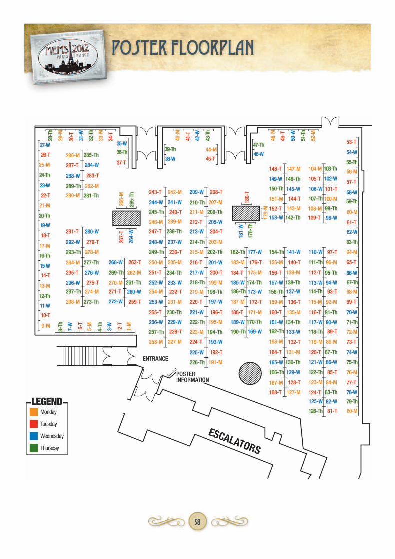
58
ESCALATORS