Embed Size (px)
Citation preview

Sundance Multiprocessor TechnologySundance Multiprocessor Technology
Sundance Multiprocessor Technology
SMT702 + SMT712
Sundance Multiprocessor Technology
Organization:
Introduction to SMT702 High-speed ADC Introduction to SMT712 High-speed DAC FPGA Configuration (SMT702/SMT712) Sundance Firmware Model SMT702 Firmware Overview SMT712 Firmware Overview SMT702 Clocks and Resets SMT712 Clocks and Resets The DDR2 ‘FIFO’ Controller Host PC Software: SMT7026 Practical Time: Questions, Help, Suggestions...
Sundance Multiprocessor Technology
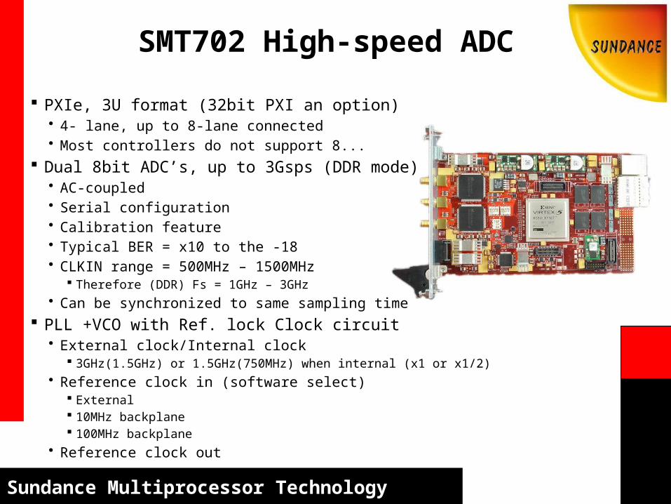
SMT702 High-speed ADC
PXIe, 3U format (32bit PXI an option)• 4- lane, up to 8-lane connected• Most controllers do not support 8...
Dual 8bit ADC’s, up to 3Gsps (DDR mode)• AC-coupled• Serial configuration• Calibration feature• Typical BER = x10 to the -18• CLKIN range = 500MHz – 1500MHz
Therefore (DDR) Fs = 1GHz – 3GHz• Can be synchronized to same sampling time
PLL +VCO with Ref. lock Clock circuit• External clock/Internal clock
3GHz(1.5GHz) or 1.5GHz(750MHz) when internal (x1 or x1/2)• Reference clock in (software select)
External 10MHz backplane 100MHz backplane
• Reference clock out

Sundance Multiprocessor Technology
SMT702 High-speed ADC Trigger
• Internal (PXIe backplane)• External (front panel)
Flash + CPLD configuration 1GB DDR2 memory x2 banks
• 64bit wide, 128M deep• Max, 333MHz (250MHz default)
SHB x2• LVTTL• 32bit + 3control +1Clock
SATA I x2 RSL x1
• 4 data channels @ 250MB/s Xilinx parallel JTAG Xilinx FPGA
• FFG1136-3 (fastest)• FX70T, LX110T (possibility for SX50T, SX95T)
All SMA connectors on front-panel

Sundance Multiprocessor Technology
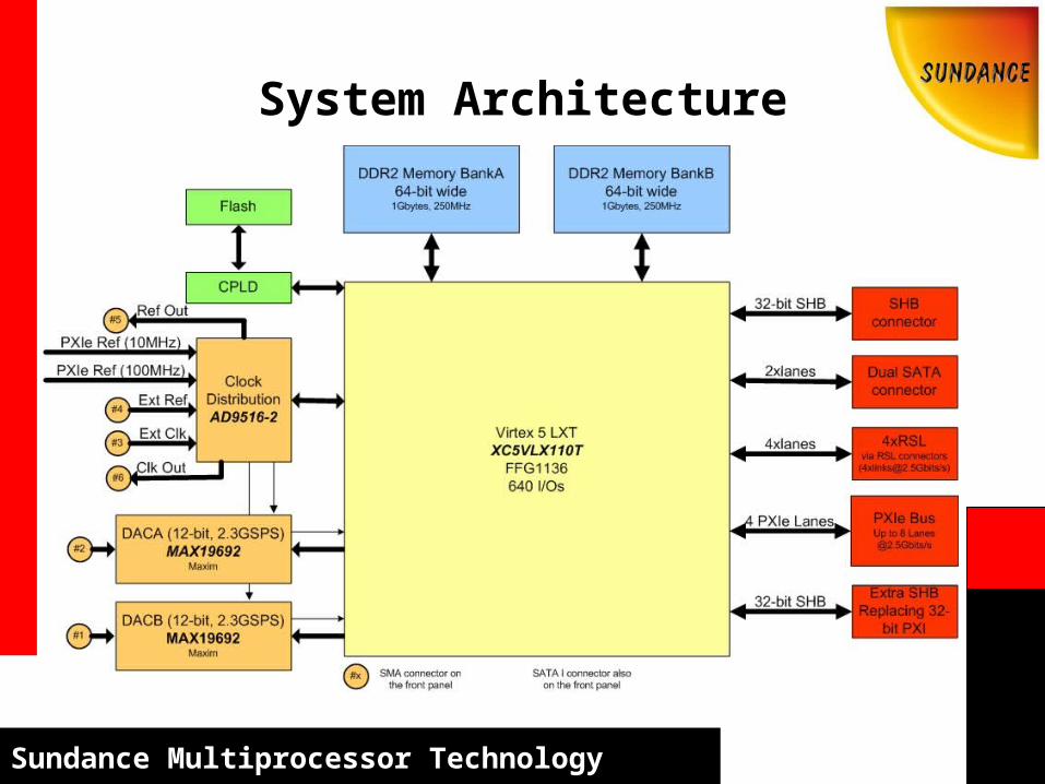
System Architecture
Sundance Multiprocessor Technology
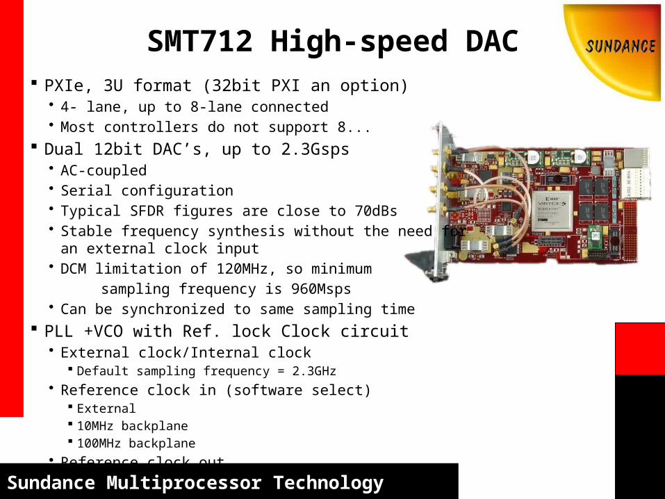
SMT712 High-speed DAC PXIe, 3U format (32bit PXI an option)
• 4- lane, up to 8-lane connected• Most controllers do not support 8...
Dual 12bit DAC’s, up to 2.3Gsps• AC-coupled• Serial configuration• Typical SFDR figures are close to 70dBs• Stable frequency synthesis without the need for an external
clock input• DCM limitation of 120MHz, so minimum sampling frequency is 960Msps• Can be synchronized to same sampling time
PLL +VCO with Ref. lock Clock circuit• External clock/Internal clock
Default sampling frequency = 2.3GHz• Reference clock in (software select)
External 10MHz backplane 100MHz backplane
• Reference clock out

Sundance Multiprocessor Technology
SMT712 High-speed DAC Trigger
• Internal (PXIe backplane)• External (front panel)
Flash + CPLD configuration 1GB DDR2 memory x2 banks
• 64bit wide, 128M deep• Max, 333MHz (250MHz default)
SHB x2• LVTTL• 32bit + 3control +1Clock
SATA I x2 RSL x1
• 4 data channels @ 250MB/s Xilinx parallel JTAG Xilinx FPGA
• FFG1136-3 (fastest)• FX70T, LX110T (possibility for SX50T, SX95T)
All SMA connectors on front-panel
Sundance Multiprocessor Technology
System Architecture

Sundance Multiprocessor Technology
Questions?
Sundance Multiprocessor TechnologySundance Multiprocessor Technology
Sundance Multiprocessor Technology
SMT702 + SMT712 FPGA Configuration
Sundance Multiprocessor Technology
CPLD + Flash Configuration The FPGA in both the SMT702 and SMT712 are configured at power up from a selectable
address in on-board flash A CPLD manages accessing the flash chip for configuration, and reading/writing from the
Host – transparent from user Flash size for both systems = 256Mbit
Sundance Multiprocessor Technology
SMT6002 The SMT6002 is the provided Host application used to access the flash chip for
loading and deleting bitstreams via a connection block in the FPGA to the CPLD. The tool will automatically detect the type of board and read the contents of the
flash when launched. The default firmware (at address 0x0) is read-only and so protected from
deletion. This is so that even after custom bitstream booting, there is always a recoverable link to the flash for correction.
Sundance Multiprocessor Technology
Changing the Flash Contents Deleting
• Select the bitstream to remove and press ‘Delete’.• There is a ‘Safe-erase’ option which will remove every bitstream in flash except for the default
bitstream at address 0x0.• There is an option to remove the entire flash, but requires a modification to the Windows Registry.
Adding• After a bitstream path has been chosen, select a position in flash to load the bitstream. With the
‘Basic’ addressing mode chosen, the offset address will be adjusted automatically for the board accessed. Comments and Version information may be optionally loaded as well if desired.
Sundance Multiprocessor Technology
Bitstream Configuration
The position offset address in flash can be chosen by switch selection (SW1).• SW1 has four, on/off switches integrated, but only toggle 1 and 2
are used. The address to be booted can be counted in binary. Position 0, (offset 0x0 default) is SW1(1 = off, 2 = off). Position 1, (offset 0x800000) is SW1(1 = off, 2 = on). Etc.
The FPGA can also be reconfigured after power up by selecting the bitstream, then ticking ‘Reconfigure FPGA from Flash’. Press ‘Commit’.
The approximate time to configure the FPGA from flash and be ‘alive’ to the Host is approximately 140ms.
Sundance Multiprocessor Technology
Questions?
The SMT6002 Help file can be found at: C:\Program Files\Sundance\SMT6002\SMT6002.chm
Sundance Multiprocessor TechnologySundance Multiprocessor Technology
Sundance Firmware
Sundance uses a FPGA to implement the communication resources. Sundance has
developed various communication resources such as PCI/PCIe, 32-bit SHB, RSL…

Sundance Multiprocessor Technology
Model Overview
Sundance uses modularity in its designs to improve reusability and maintainability. This approach creates a number of elementary blocks which are used to create the firmware.
Sundance Multiprocessor Technology
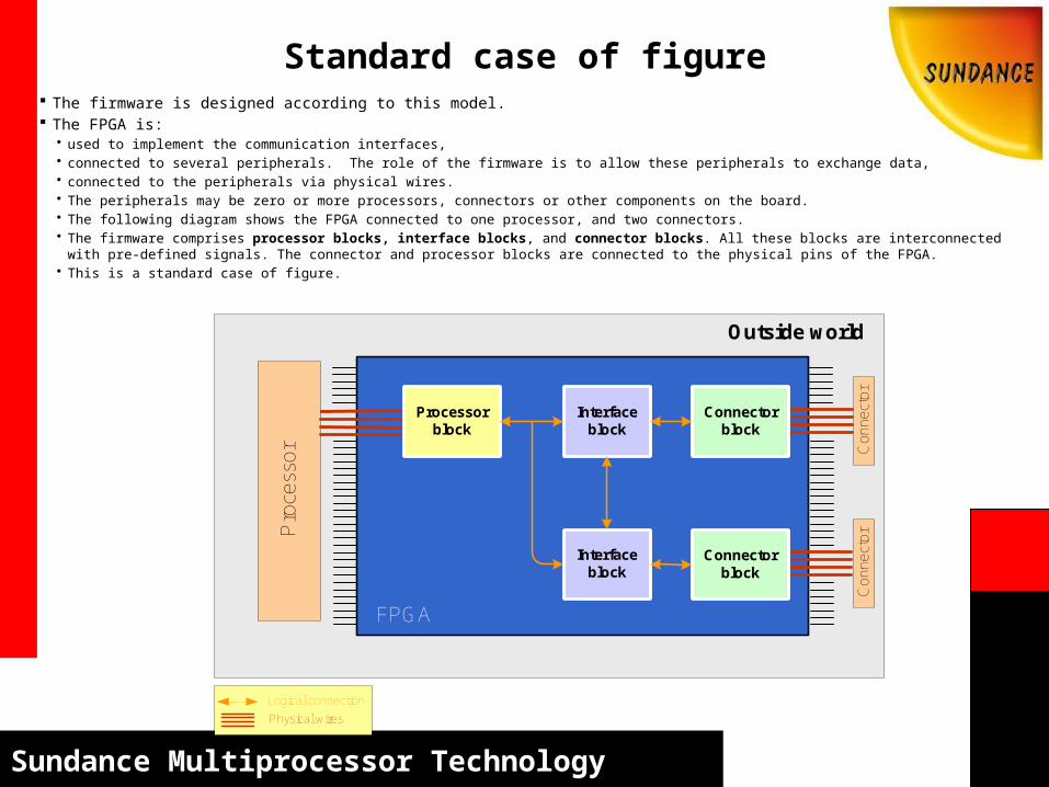
Standard case of figure The firmware is designed according to this model. The FPGA is:
• used to implement the communication interfaces, • connected to several peripherals. The role of the firmware is to allow these peripherals to exchange data, • connected to the peripherals via physical wires. • The peripherals may be zero or more processors, connectors or other components on the board.• The following diagram shows the FPGA connected to one processor, and two connectors.• The firmware comprises processor blocks, interface blocks, and connector blocks. All these blocks are interconnected with pre-defined signals. The
connector and processor blocks are connected to the physical pins of the FPGA. • This is a standard case of figure.
Interface block
Interface block
FPGA
Outside world
Pro
cess
or Con
nect
orC
onne
ctor
Connector block
Connector block
Processor block
Physical wires
Logical connection
Sundance Multiprocessor Technology
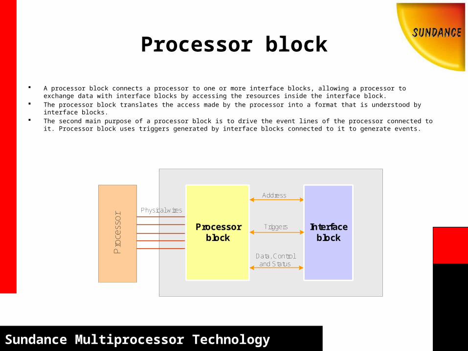
Processor block
A processor block connects a processor to one or more interface blocks, allowing a processor to exchange data with interface blocks by accessing the resources inside the interface block.
The processor block translates the access made by the processor into a format that is understood by interface blocks. The second main purpose of a processor block is to drive the event lines of the processor connected to it. Processor block uses triggers
generated by interface blocks connected to it to generate events.
Processor block
Physical wires
Pro
cess
or
Interface block
Data, Control and Status
Address
Triggers

Sundance Multiprocessor Technology
Interface block The interface block implements a collection of addressable resources (registers, and memory space mainly) that can be read or written
by a processor block. Interface blocks usually drive connector blocks. By accessing these resources, a processor block can: obtain status information about the interface block and the connector block attached to it, control the state of the interface block and the connector block, transfer data to and from the connector block. Each interface block can be connected to one processor block, one connector block, and zero or more interface blocks.
Register
Control and Status
Trigger/status
Address Register
Register
Interface block
Trigger/status
Connector block
Data
Status
Control
Data, control, and status

Sundance Multiprocessor Technology
Interface block
Processors might want to know when some condition is met inside the interface block. For example when the interface block has collected a certain number of words ready to be read. When such an event occurs, the interface block can generate a trigger. These triggers may be passed to other interface blocks and to processor blocks.
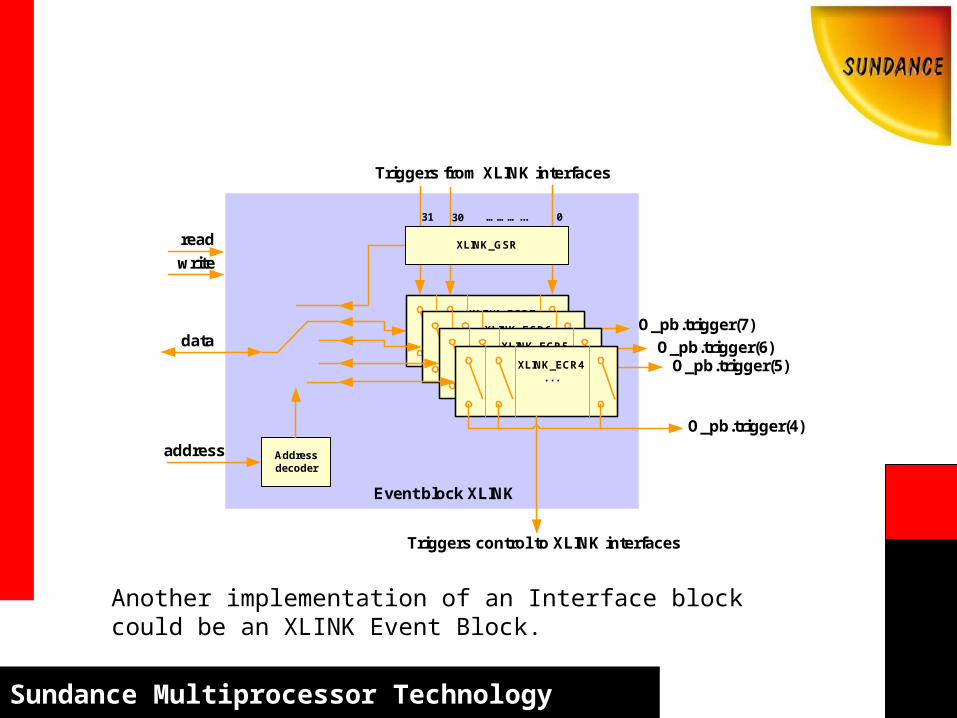
Some interface blocks, called event blocks, are dedicated to gather triggers and status information from other interface blocks, and to present them to a processor block. For example gathering the status and trigger information for all the XLINK interfaces in the system. Typically, these interface blocks allow the user to select which trigger conditions should be passed to the processor block.
To indicate to a processor that a trigger condition has been met, the processor block uses event lines to the processor. The processor block may drive these event lines when the interface blocks connected to it present a trigger condition.
Sundance Multiprocessor Technology
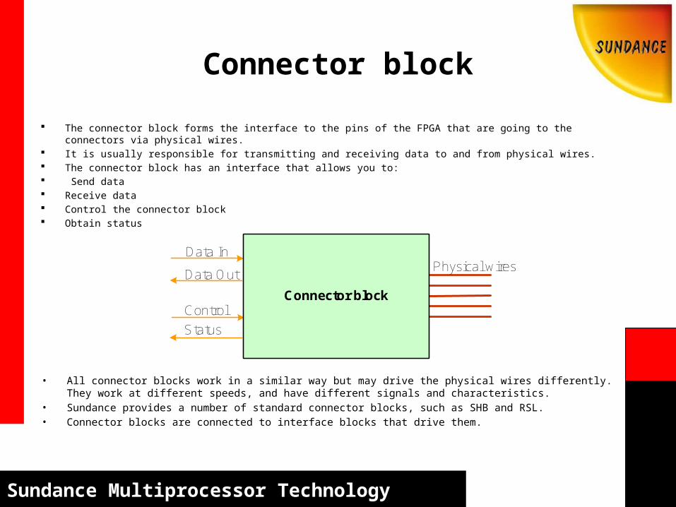
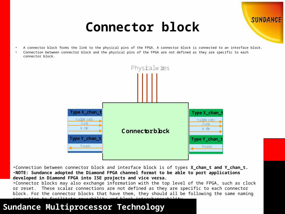
Connector block
The connector block forms the interface to the pins of the FPGA that are going to the connectors via physical wires. It is usually responsible for transmitting and receiving data to and from physical wires. The connector block has an interface that allows you to: Send data Receive data Control the connector block Obtain status
Physical wiresData In
Status
Control
Data Out
Connector block
• All connector blocks work in a similar way but may drive the physical wires differently. They work at different speeds, and have different signals and characteristics.
• Sundance provides a number of standard connector blocks, such as SHB and RSL. • Connector blocks are connected to interface blocks that drive them.
Sundance Multiprocessor Technology
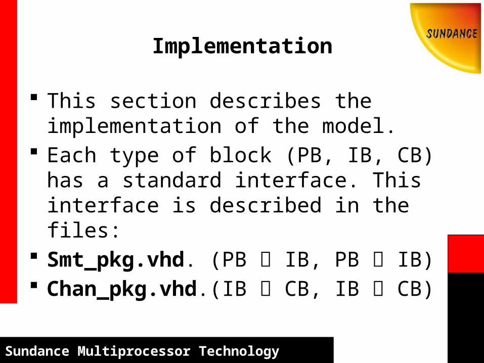
Implementation
This section describes the implementation of the model.
Each type of block (PB, IB, CB) has a standard interface. This interface is described in the files:
Smt_pkg.vhd. (PB IB, PB IB) Chan_pkg.vhd.(IB CB, IB CB)
Sundance Multiprocessor Technology
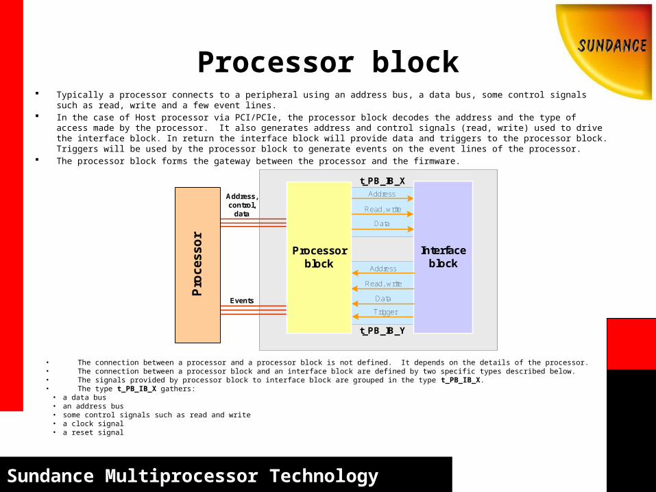
Processor block Typically a processor connects to a peripheral using an address bus, a data bus, some control signals such as read, write and a few
event lines. In the case of Host processor via PCI/PCIe, the processor block decodes the address and the type of access made by the processor. It
also generates address and control signals (read, write) used to drive the interface block. In return the interface block will provide data and triggers to the processor block. Triggers will be used by the processor block to generate events on the event lines of the processor.
The processor block forms the gateway between the processor and the firmware.
Interface block
Data
Address
Read, write
Pro
cess
or
Trigger
Data
Address
Read, write
Address, control,
data
Events
Processor block
t_PB_IB_Y
t_PB_IB_X
• The connection between a processor and a processor block is not defined. It depends on the details of the processor. • The connection between a processor block and an interface block are defined by two specific types described below. • The signals provided by processor block to interface block are grouped in the type t_PB_IB_X. • The type t_PB_IB_X gathers:
• a data bus • an address bus • some control signals such as read and write • a clock signal • a reset signal
Sundance Multiprocessor Technology
Interface block
The interface block is connected to a processor block. Each interface block has a region of the processor block’s memory space associated with it. When an access is made in this memory range, the interface block is responsible for dealing with the access. The allocation of the range of memory of an interface block can be done by specifying the properties of this interface block.
The properties allow to specify the start and the end address of the interface block. This is defined in the type t_IBProperties. This is the way the memory mapping of interface blocks is done.
Interface blocks can implement functionality that is accessed by means of resources inside the memory space associated with it. These resources can be used to control the interface block, to obtain status and to communicate data with other blocks further down in the design.
The pre-defined collection of addressable resources implemented by an interface block is called an “interface” from a software point of view. The software interfaces are described in the SMT6400 package, and in the SMT6025 for the XLINK interface block and the IB_reg.
Interface blocks can be used to drive a connector block. Interface block and connector block are connected via a “data type” connection.
Sundance Multiprocessor Technology
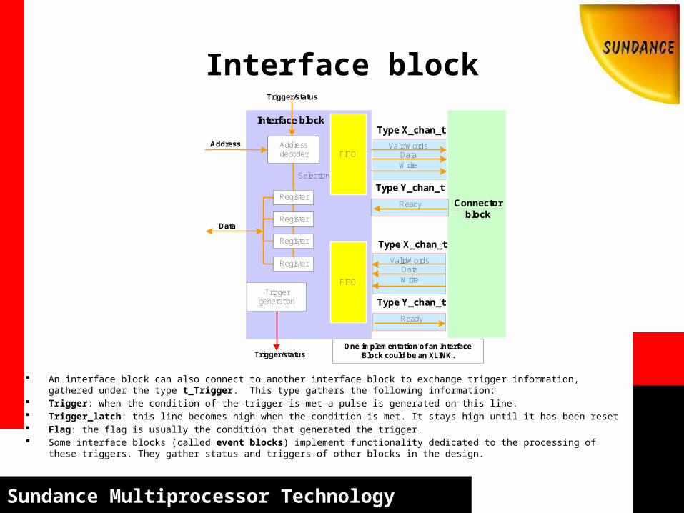
Interface block
An interface block can also connect to another interface block to exchange trigger information, gathered under the type t_Trigger. This type gathers the following information:
Trigger: when the condition of the trigger is met a pulse is generated on this line. Trigger_latch: this line becomes high when the condition is met. It stays high until it has been reset Flag: the flag is usually the condition that generated the trigger. Some interface blocks (called event blocks) implement functionality dedicated to the processing of these triggers. They gather status
and triggers of other blocks in the design.
Trigger/status
Address
Register
Interface block
Trigger/status
Write
Data
Trigger generation
Register
Register
Register
Address decoder
Selection
Data
Type X_chan_t
Connector block
ValidWords
Ready
Type Y_chan_t
WriteData
Type X_chan_t
ValidWords
Ready
Type Y_chan_t
FIFO
FIFO
One implementation of an Interface Block could be an XLINK.
Sundance Multiprocessor Technology
Address
Interface block
Trigger/status
Read/write
Data
Address decoder
SelectionAddress
Data
Connector block
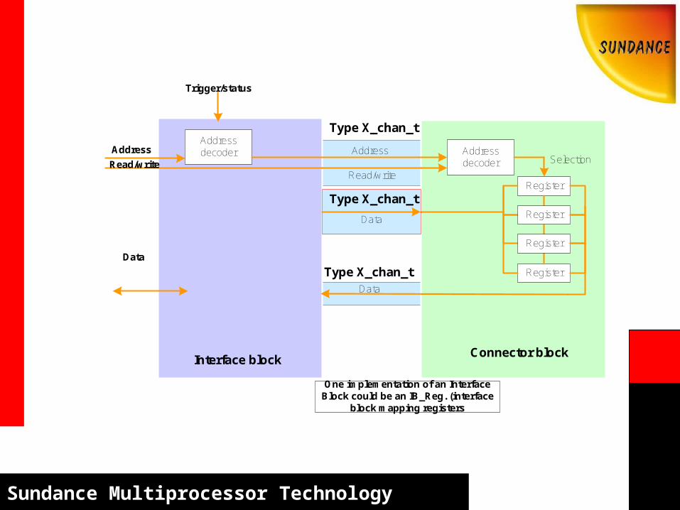
One implementation of an Interface Block could be an IB_Reg. (interface
block mapping registers
Register
Register
Type X_chan_t
Data
Type X_chan_t
Register
Register
Address decoder
Type X_chan_t
Read/write
Sundance Multiprocessor Technology
data
address Address decoder
Event block XLINK
read
write
Triggers from XLINK interfaces
O_pb.trigger(5)O_pb.trigger(6)
O_pb.trigger(7)XLINK_ECR7
. . .XLINK_ECR6. . .XLINK_ECR5
. . .XLINK_ECR4. . .
XLINK_GSR
O_pb.trigger(4)
Triggers control to XLINK interfaces
3031 0………...
Another implementation of an Interface block could be an XLINK Event Block.
Sundance Multiprocessor Technology
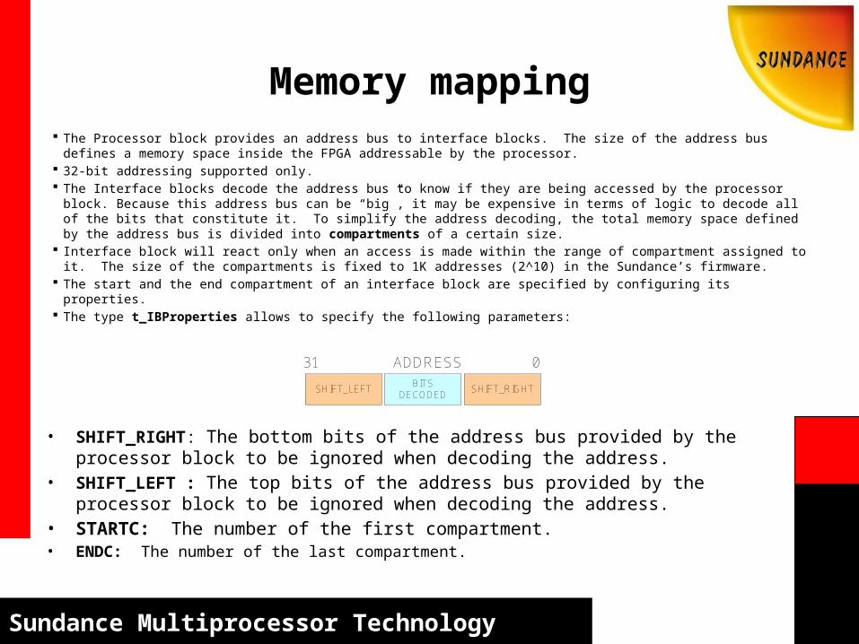
Memory mapping The Processor block provides an address bus to interface blocks. The size of the address bus defines a memory
space inside the FPGA addressable by the processor. 32-bit addressing supported only. The Interface blocks decode the address bus to know if they are being accessed by the processor block. Because this
address bus can be “big”, it may be expensive in terms of logic to decode all of the bits that constitute it. To simplify the address decoding, the total memory space defined by the address bus is divided into compartments of a certain size.
Interface block will react only when an access is made within the range of compartment assigned to it. The size of the compartments is fixed to 1K addresses (2^10) in the Sundance’s firmware.
The start and the end compartment of an interface block are specified by configuring its properties. The type t_IBProperties allows to specify the following parameters:
BITS DECODED
SHIFT_RIGHTSHIFT_LEFT
31 0ADDRESS
• SHIFT_RIGHT: The bottom bits of the address bus provided by the processor block to be ignored when decoding the address.
• SHIFT_LEFT : The top bits of the address bus provided by the processor block to be ignored when decoding the address.
• STARTC: The number of the first compartment.• ENDC: The number of the last compartment.
Sundance Multiprocessor Technology
0
1
2
16
17
18
19
.
.
.
.
.
.
Start
End
StartEnd
Start
End
IB_0
XLINK
IB_3
(31-SHIFT_RIGHT) - SHIFT_LEFT
(31-SHIFT_RIGHT) - SHIFT_LEFT
(31-SHIFT_RIGHT) - SHIFT_LEFT
Memory mapping
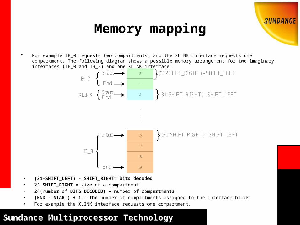
For example IB_0 requests two compartments, and the XLINK interface requests one compartment. The following diagram shows a possible memory arrangement for two imaginary interfaces (IB_0 and IB_3) and one XLINK interface.
• (31-SHIFT_LEFT) - SHIFT_RIGHT= bits decoded• 2^ SHIFT_RIGHT = size of a compartment.• 2^(number of BITS DECODED) = number of compartments.• (END – START) + 1 = the number of compartments assigned to the Interface block.• For example the XLINK interface requests one compartment.
Sundance Multiprocessor Technology
Connector block
Physical wires
Connector blockWriteData
Type X_chan_t
ValidWords
Ready
Type Y_chan_t
WriteData
Type X_chan_t
ValidWords
Ready
Type Y_chan_t
•Connection between connector block and interface block is of types X_chan_t and Y_chan_t. •NOTE: Sundance adopted the Diamond FPGA channel format to be able to port applications developed in Diamond FPGA into ISE projects and vice versa.•Connector blocks may also exchange information with the top level of the FPGA, such as clock or reset. These scalar connections are not defined as they are specific to each connector block. For the connector blocks that have them, they should all be following the same naming convention to facilitate reusability and block interchangeability.
• A connector block forms the link to the physical pins of the FPGA. A connector block is connected to an interface block.• Connection between connector block and the physical pins of the FPGA are not defined as they are specific to each connector block.
Sundance Multiprocessor Technology
Summary of FPGA Channels defined in the 3L Diamond Help file
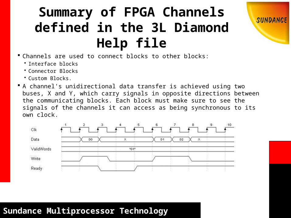
Channels are used to connect blocks to other blocks: • Interface blocks• Connector Blocks• Custom Blocks.
A channel's unidirectional data transfer is achieved using two buses, X and Y, which carry signals in opposite directions between the communicating blocks. Each block must make sure to see the signals of the channels it can access as being synchronous to its own clock.

Sundance Multiprocessor Technology
The Types
The following table describes the signals constituting each of the types used to implement the firmware.
Signal Length (bits) Description
t_PB_IB_Xsignals going from the Processor Block to the Interface Block
CLK 1 Clock signal. The clock provided by the processor block to the interface blocks. The signals of the type t_PB_IB_X are synchronous to this clock.
RST 1 Reset signal used to reset the interface blocks.
ADDR 32 Address bus.
DATA 32 Data bus.
READ 1 Read command signal.
WRITE 1 Write command signal.
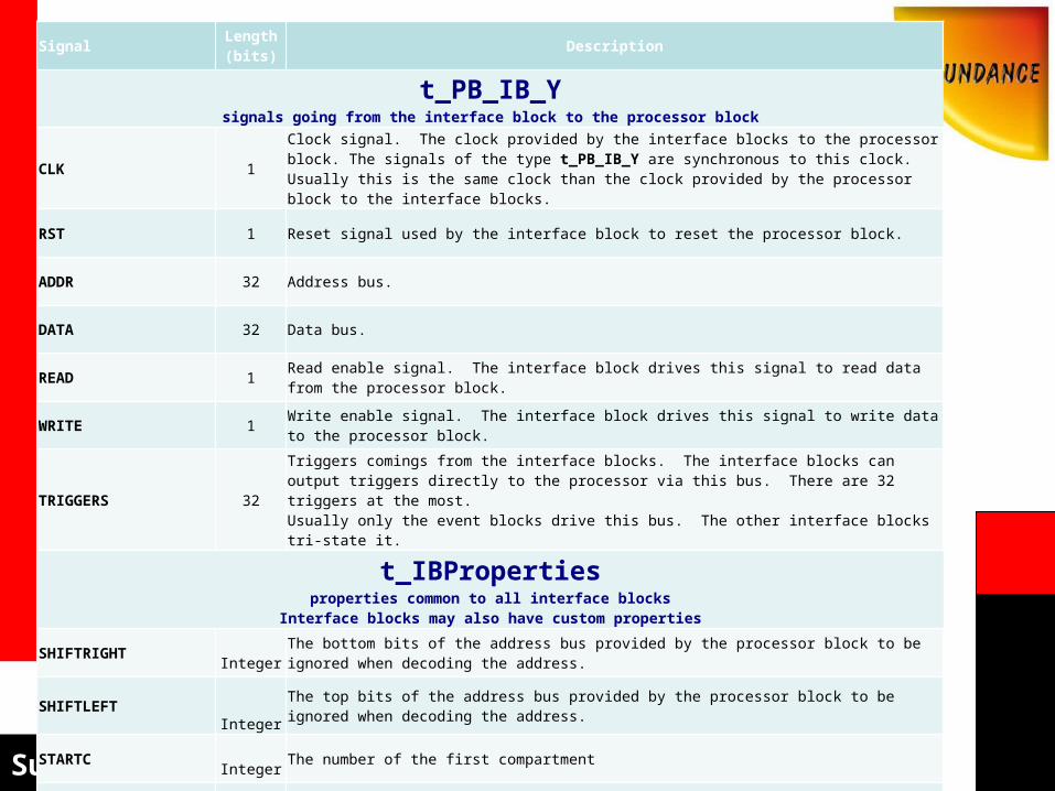
Sundance Multiprocessor Technology
Signal Length (bits) Description
t_PB_IB_Ysignals going from the interface block to the processor block
CLK 1Clock signal. The clock provided by the interface blocks to the processor block. The signals of the type t_PB_IB_Y are synchronous to this clock. Usually this is the same clock than the clock provided by the processor block to the interface blocks.
RST 1 Reset signal used by the interface block to reset the processor block.
ADDR 32 Address bus.
DATA 32 Data bus.
READ 1 Read enable signal. The interface block drives this signal to read data from the processor block.
WRITE 1 Write enable signal. The interface block drives this signal to write data to the processor block.
TRIGGERS 32Triggers comings from the interface blocks. The interface blocks can output triggers directly to the processor via this bus. There are 32 triggers at the most.Usually only the event blocks drive this bus. The other interface blocks tri-state it.
t_IBPropertiesproperties common to all interface blocks
Interface blocks may also have custom properties
SHIFTRIGHT Integer The bottom bits of the address bus provided by the processor block to be ignored when decoding the address.
SHIFTLEFT Integer The top bits of the address bus provided by the processor block to be ignored when decoding the address.
STARTC Integer The number of the first compartment
ENDC Integer The number of the last compartment
Sundance Multiprocessor Technology
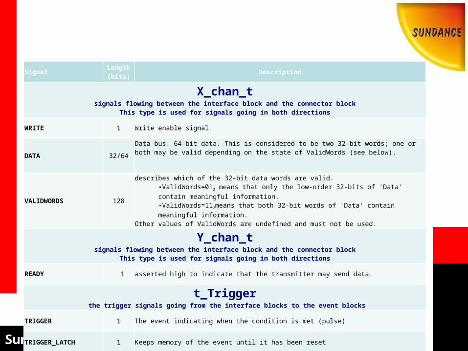
Signal Length (bits) Description
X_chan_tsignals flowing between the interface block and the connector block
This type is used for signals going in both directions
WRITE 1 Write enable signal.
DATA 32/64Data bus. 64-bit data. This is considered to be two 32-bit words; one or both may be valid depending on the state of ValidWords (see below).
VALIDWORDS 128
describes which of the 32-bit data words are valid.•ValidWords=012 means that only the low-order 32-bits of 'Data' contain meaningful information.•ValidWords=112means that both 32-bit words of 'Data' contain meaningful information.
Other values of ValidWords are undefined and must not be used.
Y_chan_tsignals flowing between the interface block and the connector block
This type is used for signals going in both directions
READY 1 asserted high to indicate that the transmitter may send data.
t_Trigger the trigger signals going from the interface blocks to the event blocks
TRIGGER 1 The event indicating when the condition is met (pulse)
TRIGGER_LATCH 1 Keeps memory of the event until it has been reset
FLAG 1 Usually the condition that generated the trigger

Sundance Multiprocessor Technology
SMT702 FIRMWARE
We assume you read and understood the documents given previously. Processor block: Interface to the Pcie bus. XILINX_PCI_EXP_EP
Interface blocks :XLINKs, IB_Reg, IB_TOC Properties:
• IB_XLINK PROPERTIES in Smt7xx_XLink_Init_pkg.• IBToc PROPERTIES in IB_pkg.• IB_Reg PROPERTIES in IBReg_SMT7xx.
Connector blocks: • Register blocks: CB90_SMT7xx.vhd, CB_SMT702.vhd, CB_TOC_SMT7xx • Memory interface: DataPathDDR2FIFO.vhd.• serial interfaces.
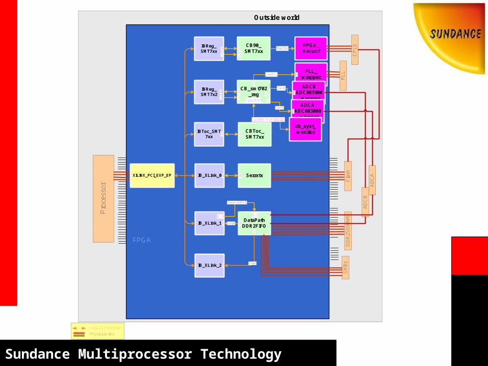
Sundance Multiprocessor Technology
IB_XLink_0
IB_XLink_1
FPGA
Outside world
Pro
cess
or
Fla
sh
DataPath DDR2FIFO
SerrxtxXILINX_PCI_EXP_EP
Physical wires
Logical connection
IB_XLink_2DataB
DataA
IBReg_ SMT7x2
IBToc_SMT7xx
CBToc_ SMT7xx
CB_smt702_reg
IBReg_ SMT7xx
CB90_ SMT7xx
Conf B
PLL_wrapper
Conf PLL
ADCBADC083000_wrapper
ADCAADC083000_wrapper
PL
L
AD
CB
AD
CA
Phase shift A,B
Sys_mon
0, 1
1
2
0
0
0
3
1
00
1
00
1
00
00
00
0
Conf A
cb_syst_ monitor
11
System monitor ios
SH
Bs
DD
R2S
DR
AM
FPGA_ Reconf
Reconf
CP
LD
0, 1

Sundance Multiprocessor Technology
SMT702 Firmware Memory mapping
The SMT702 memory mapping follows the table below.
4 bits 10 bits18 bits
31 0
ADDRESS
14 13 10 9
0
1
5
6
7
8
.
.
.
Start
End
IB_Reg_SMT7xxStart
End
IB_Reg_SMT7x2
4
1K Byte
EndIB_Toc_SMT7xx
Start
EndIB_XLINK_0
Start
EndIB_XLINK_1
Start
EndIB_XLINK_2
Start
EndIB_XLINK_3
Start
9Start
EndEB_XLink_w

Sundance Multiprocessor Technology
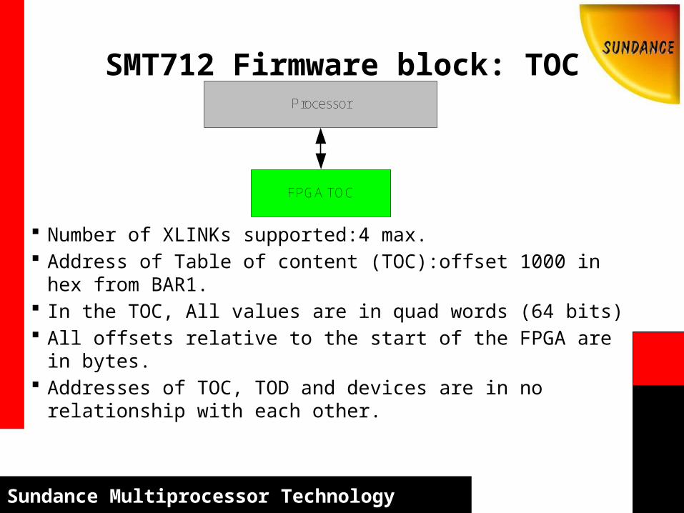
SMT702 Firmware block: TOC
Number of XLINKs supported:4 max. Address of Table of content (TOC):offset 1000 in hex from
BAR1. In the TOC, All values are in quad words (64 bits) All offsets relative to the start of the FPGA are in bytes. Addresses of TOC, TOD and devices are in no relationship with
each other.
FPGA TOC
Processor
Sundance Multiprocessor Technology
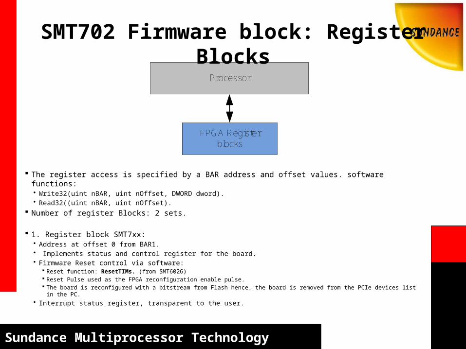
The register access is specified by a BAR address and offset values. software functions:• Write32(uint nBAR, uint nOffset, DWORD dword).• Read32((uint nBAR, uint nOffset).
Number of register Blocks: 2 sets.
1. Register block SMT7xx:• Address at offset 0 from BAR1.• Implements status and control register for the board.• Firmware Reset control via software:
Reset function: ResetTIMs. (from SMT6026) Reset Pulse used as the FPGA reconfiguration enable pulse. The board is reconfigured with a bitstream from Flash hence, the board is removed from the PCIe devices list in the PC.
• Interrupt status register, transparent to the user.
FPGA Register blocks
Processor
SMT702 Firmware block: Register Blocks
Sundance Multiprocessor Technology
2. Register Block SMT702:• Address at offset 400 in hex from BAR1.• Implements specific functionalities proper to the
SMT702, see a description in the SMT702 User Guide.
• Reset: Reset Pulse with a delay to give time to the Hardware
to propagate the reset and clear all the IB FIFOs . Does not reset the PCIe core to prevent loosing the
board on the bus.
Sundance Multiprocessor Technology
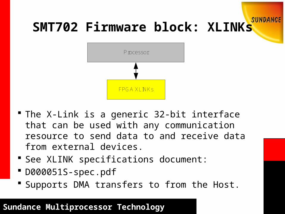
The X-Link is a generic 32-bit interface that can be used with any communication resource to send data to and receive data from external devices.
See XLINK specifications document: D000051S-spec.pdf Supports DMA transfers to from the Host.
FPGA XLINKs
Processor
SMT702 Firmware block: XLINKs
Sundance Multiprocessor Technology
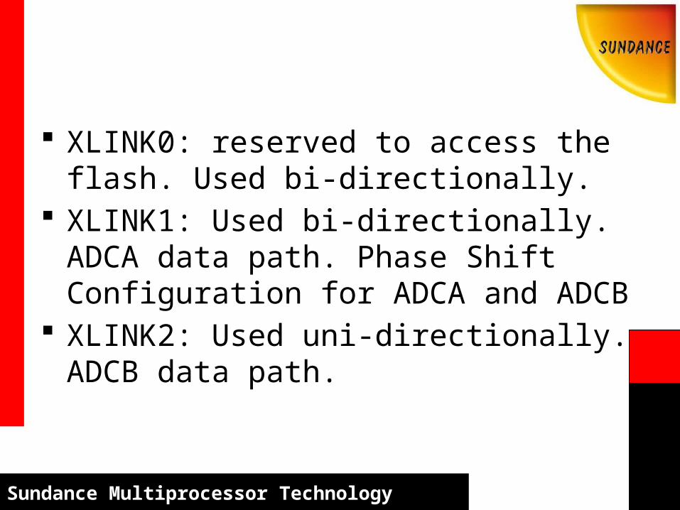
XLINK0: reserved to access the flash. Used bi-directionally.
XLINK1: Used bi-directionally. ADCA data path. Phase Shift Configuration for ADCA and ADCB
XLINK2: Used uni-directionally. ADCB data path.
Sundance Multiprocessor Technology
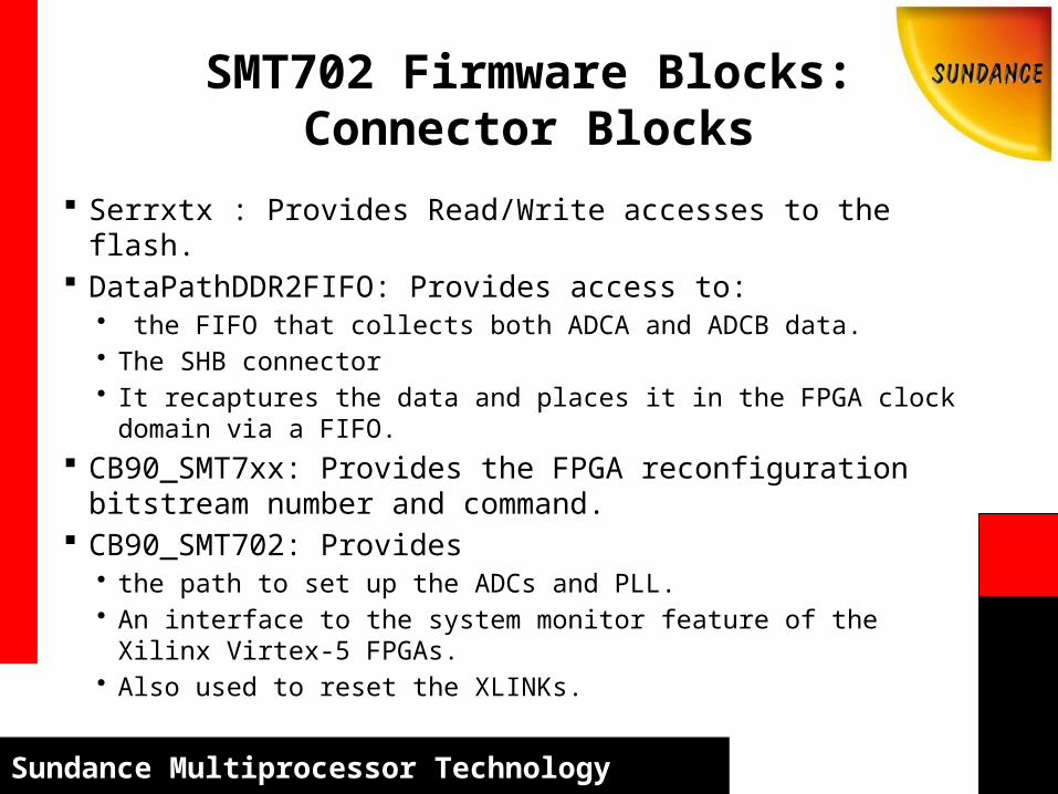
SMT702 Firmware Blocks: Connector Blocks
Serrxtx : Provides Read/Write accesses to the flash. DataPathDDR2FIFO: Provides access to:
• the FIFO that collects both ADCA and ADCB data.• The SHB connector• It recaptures the data and places it in the FPGA clock domain via a
FIFO. CB90_SMT7xx: Provides the FPGA reconfiguration bitstream
number and command. CB90_SMT702: Provides
• the path to set up the ADCs and PLL. • An interface to the system monitor feature of the Xilinx Virtex-5 FPGAs.• Also used to reset the XLINKs.
Sundance Multiprocessor Technology
SMT712 FIRMWARE
We assume you read and understood the documents given previously. Processor block: Interface to the Pcie bus. XILINX_PCI_EXP_EP
Interface blocks :XLINKs, IB_Reg, IB_TOC Properties:
• IB_XLINK PROPERTIES in Smt7xx_XLink_Init_pkg.• IBToc PROPERTIES in IB_pkg.• IB_Reg PROPERTIES in IBReg_SMT7xx.
Connector blocks: • Register blocks: CB90_SMT7xx.vhd, CB_SMT712.vhd, CB_TOC_SMT7xx • Memory interface: DACDDR2DataPath.vhd.• serial interfaces.

Sundance Multiprocessor Technology
IB_XLink_0
IB_XLink_1
FPGA
Outside world
Pro
cess
or
Fla
sh
DACDDR2 DataPath
SerrxtxXILINX_PCI_EXP_EP
Physical wires
Logical connection
IB_XLink_2Data B
Data A
IBReg_ SMT7x2
IBToc_SMT7xx
CBToc_ SMT7xx
CB_smt712_reg
IBReg_ SMT7xx
CB90_ SMT7xx
ConfAD9516_ wrapper
DA
C
Phase shift A,B
Sys_mon
0, 1
1 0
1
00
1
00
3
00
00
20
0
cb_syst_ monitor
11
System monitor
SH
Bs
DD
R2S
DR
AM
FPGA_ Reconf
Reconf
CP
LD
2, 3
Sundance Multiprocessor Technology
SMT712 Firmware Memory mapping
The SMT712 memory mapping follows the table below.
4 bits 10 bits18 bits
31 0
ADDRESS
14 13 10 9
0
1
5
6
7
8
.
.
.
Start
End
IB_Reg_SMT7xxStart
End
IB_Reg_SMT7x2
4
1K Byte
EndIB_Toc_SMT7xx
Start
EndIB_XLINK_0
Start
EndIB_XLINK_1
Start
EndIB_XLINK_2
Start
EndIB_XLINK_3
Start
9Start
EndEB_XLink_w
Sundance Multiprocessor Technology
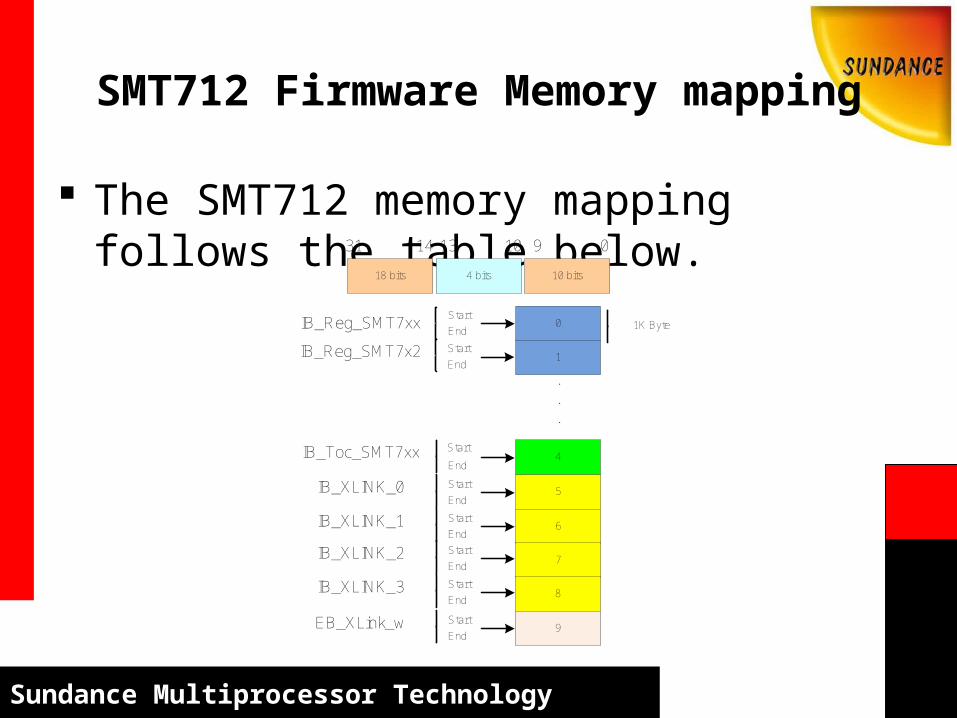
SMT712 Firmware block: TOC
Number of XLINKs supported:4 max. Address of Table of content (TOC):offset 1000 in hex from
BAR1. In the TOC, All values are in quad words (64 bits) All offsets relative to the start of the FPGA are in bytes. Addresses of TOC, TOD and devices are in no relationship with
each other.
FPGA TOC
Processor

Sundance Multiprocessor Technology
The register access is specified by a BAR address and offset values. software functions:• Write32(uint nBAR, uint nOffset, DWORD dword).• Read32((uint nBAR, uint nOffset).
Number of register Blocks: 2 sets.
1. Register block SMT7xx:• Address at offset 0 from BAR1.• Implements status and control register for the board.• Firmware Reset control via software:
Reset function: ResetTIMs. (from SMT6026) Reset Pulse used as the FPGA reconfiguration enable pulse. The board is reconfigured with a bitstream from Flash hence, the board is removed from the PCIe devices list in the PC.
• Interrupt status register, transparent to the user.
FPGA Register blocks
Processor
SMT712 Firmware block: Register Blocks

Sundance Multiprocessor Technology
2. Register Block SMT712:• Address at offset 400 in hex from BAR1.• Implements specific functionalities proper to the
SMT712, see a description in the SMT712 User Guide.
• Reset: Reset Pulse with a delay to give time to the Hardware
to propagate the reset and clear all the IB FIFOs . Does not reset the PCIe core to prevent loosing the
board on the bus.

Sundance Multiprocessor Technology
The X-Link is a generic 32-bit interface that can be used with any communication resource to send data to and receive data from external devices.
See XLINK specifications document: D000051S-spec.pdf Supports DMA transfers to from the Host.
FPGA XLINKs
Processor
SMT712 Firmware block: XLINKs
Sundance Multiprocessor Technology
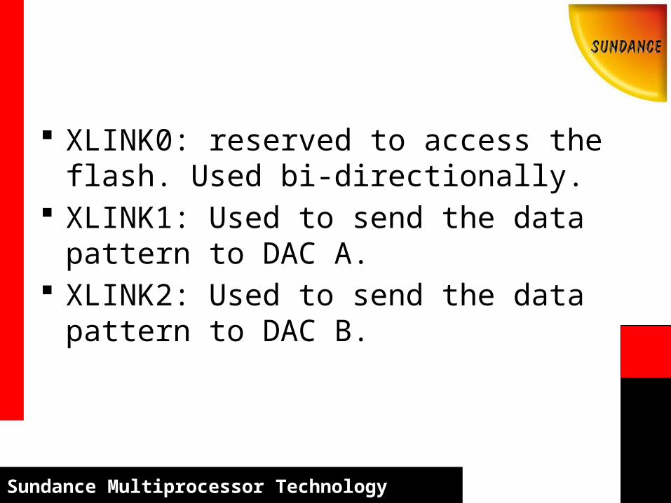
XLINK0: reserved to access the flash. Used bi-directionally.
XLINK1: Used to send the data pattern to DAC A.
XLINK2: Used to send the data pattern to DAC B.
Sundance Multiprocessor Technology
SMT712 Firmware Blocks: Connector Blocks
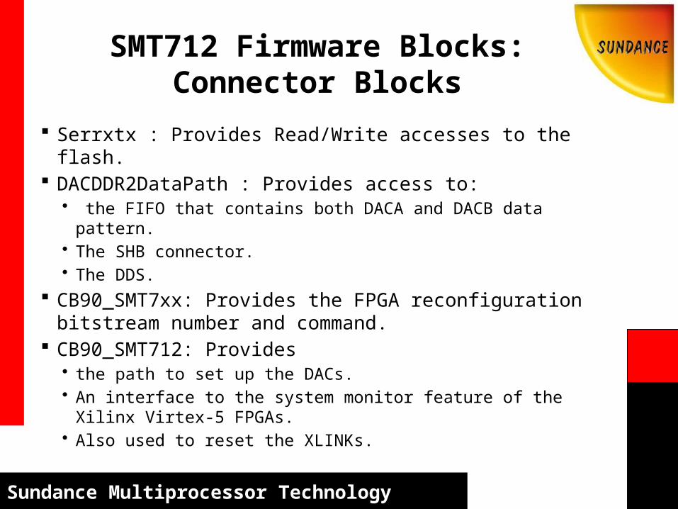
Serrxtx : Provides Read/Write accesses to the flash. DACDDR2DataPath : Provides access to:
• the FIFO that contains both DACA and DACB data pattern.• The SHB connector.• The DDS.
CB90_SMT7xx: Provides the FPGA reconfiguration bitstream number and command.
CB90_SMT712: Provides • the path to set up the DACs. • An interface to the system monitor feature of the Xilinx Virtex-5
FPGAs.• Also used to reset the XLINKs.

Sundance Multiprocessor Technology
Questions?
Sundance Multiprocessor TechnologySundance Multiprocessor Technology
SMT702 and SMT712Clocks and Reset
Synchronous Data Acquisition and Output

Sundance Multiprocessor Technology
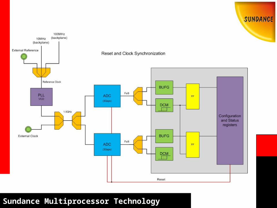
SMT702 Operation Clock Circuitry
• PLL+VCO ensures stable fixed sampling frequency, maxed to 1.5GHz (Fs=3GHz) Possible to output Clock/2 = 750MHz (Fs=1.5GHz)
• No External clock needed this way, but can be chosen through software
• Reference clock can be external or 10MHz/100MHz from backplane (software selected)
• Clock period from ADC is Fs/4 (1.5GHz/4 = 375MHz)
Sundance Multiprocessor Technology
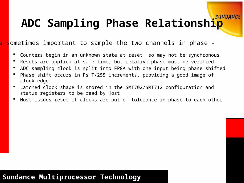
ADC Sampling Phase Relationship
Counters begin in an unknown state at reset, so may not be synchronous Resets are applied at same time, but relative phase must be verified ADC sampling clock is split into FPGA with one input being phase shifted Phase shift occurs in Fs T/255 increments, providing a good image of clock edge Latched clock shape is stored in the SMT702/SMT712 configuration and status registers to
be read by Host Host issues reset if clocks are out of tolerance in phase to each other
It is sometimes important to sample the two channels in phase -
Sundance Multiprocessor Technology

Sundance Multiprocessor Technology
Host Controlled Steps to Synchronous Reset
ADC reset is issued from Host• FSM issues a reset to ADC’s, DCM’s, and all logic depending on these clocks
After reset from Host to ADC is released, DCM’s and logic are held in reset until clock is available from ADC’s
When DCM’s lock onto ADC clock, all logic resets are released
Sundance Multiprocessor Technology
Sundance Multiprocessor Technology
DCM A is phase shifted 255 times from Host• The clock provided by each ADC through a BUFG is latched with this clock,
providing a good image of the clock edge of one full period of each clock The Host reads these 255 values (‘1’ or ‘0’) and counts (XOR’s) the
values between each sampled clock to find out how far off the phase relationship is between each Fs
If it is within tolerance the loop quits, otherwise another reset is issued and the clock is scanned again (phase shifted)
Sundance Multiprocessor Technology
Final Phase-shift is for Data Capture
Once the ADC’s are aligned to each other, the clock needs to be phase shifted again• The clock needs to be aligned correctly to the capture window of the data• Because they are both in sync, the same clock can be used for both ADC’s
External clock requirements• The default value in the software works with the onboard VCO+PLL circuitry• A different frequency needs a different phase shift• Trial and error recapture
Sundance Multiprocessor Technology
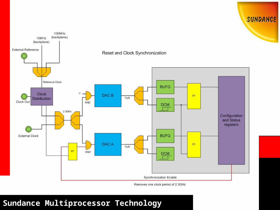
SMT712 Operation
Clock Circuitry• PLL+VCO ensures a stable fixed sampling frequency,
maxed to 2.3GHz• An additional clock out of clock circuitry is provided for
system synchronization (e.g. SMT702 synchronization)• No external clock needed this way, but can be chosen
through software• Reference clock can be external or 10MHz/100MHz
from backplane (software selected)• Clock period from DAC is Fs/8 (2.3GHz/8 = 287.5MHz)
Sundance Multiprocessor Technology
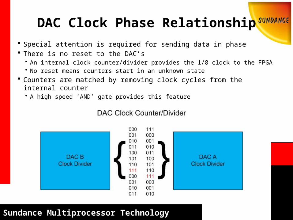
DAC Clock Phase Relationship Special attention is required for sending data in phase There is no reset to the DAC’s
• An internal clock counter/divider provides the 1/8 clock to the FPGA• No reset means counters start in an unknown state
Counters are matched by removing clock cycles from the internal counter• A high speed ‘AND’ gate provides this feature
Sundance Multiprocessor Technology
Sundance Multiprocessor Technology
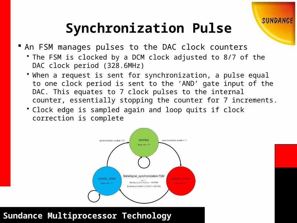
Synchronization Pulse An FSM manages pulses to the DAC clock counters
• The FSM is clocked by a DCM clock adjusted to 8/7 of the DAC clock period (328.6MHz)
• When a request is sent for synchronization, a pulse equal to one clock period is sent to the ‘AND’ gate input of the DAC. This equates to 7 clock pulses to the internal counter, essentially stopping the counter for 7 increments.
• Clock edge is sampled again and loop quits if clock correction is complete

Sundance Multiprocessor Technology
Clocked DAC A and B Phase
Clock edge is sampled the same way as the SMT702• Sampling clock for each DAC is split into a BUFG and a DCM• The DCM is phase shifted over a whole period 255 times• Latched edge is stored to SMT702/SMT712 configuration and staus
registers to be read by Host• A software ‘XOR’ of these samples determines relative phase• Because there is no reset, the Host instead issues a force synchronization
pulse

Sundance Multiprocessor Technology

Sundance Multiprocessor Technology
Sundance Multiprocessor Technology
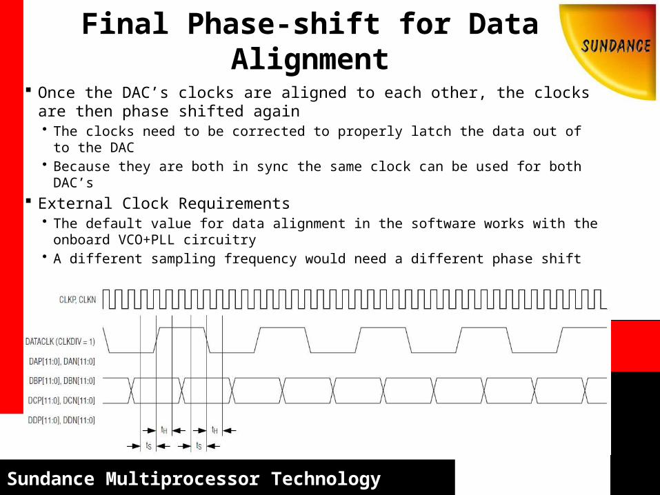
Final Phase-shift for Data Alignment
Once the DAC’s clocks are aligned to each other, the clocks are then phase shifted again• The clocks need to be corrected to properly latch the data out of to the DAC• Because they are both in sync the same clock can be used for both DAC’s
External Clock Requirements• The default value for data alignment in the software works with the onboard
VCO+PLL circuitry• A different sampling frequency would need a different phase shift

Sundance Multiprocessor Technology
Questions?

Sundance Multiprocessor TechnologySundance Multiprocessor Technology
SMT702 and SMT712DDR2 Memory Interface
smtxxx_ddr2_interface.ngcFIFO Wrapper
Sundance Multiprocessor Technology
smtXXX_ddr2_interface.ngc
The provided netlist is a wrapper modelling a FIFO, making memory transactions transparent• It provides an interface to the Xilinx CoreGenerator MIG 2.0
The best place for information on the MIG is the Xilinx provided datasheets• The provided mechanism for writing and reading from memory behaves as a FIFO
would, with DDR data• The usual expected FIFO flags and lines are available to the top of the component
Write clock, Read clock Reset Data in, Data out Empty, Full Write enable, Read enable Etc.
The difference in behaviour from a FIFO is reading and writing at the same time
The wrapper has small FIFO’s inside the netlist that allow for some leeway in this respect, but to avoid complications, the interface should be viewed as a ‘duplex’ system. (i.e. read or write at one time, but not both)

Sundance Multiprocessor Technology

Sundance Multiprocessor Technology
Questions?
Sundance Multiprocessor TechnologySundance Multiprocessor Technology
SMT702 and SMT712Host Application Environment
SMT7026
Sundance Multiprocessor Technology
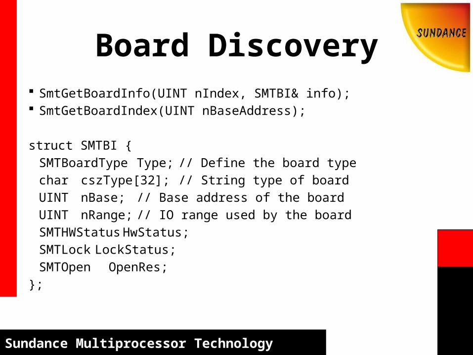
Board Discovery SmtGetBoardInfo(UINT nIndex, SMTBI& info); SmtGetBoardIndex(UINT nBaseAddress);
struct SMTBI {SMTBoardType Type;// Define the board typechar cszType[32]; // String type of board UINT nBase; // Base address of the boardUINT nRange; // IO range used by the boardSMTHWStatus HwStatus;SMTLock LockStatus;SMTOpen OpenRes;
};

Sundance Multiprocessor Technology
Board DiscoveryThese functions and structures recover the base address (BAR 1) of the first SMT board discovered on the PXIe bus. The application scans the PXIe bus and steps the pointer until the SMT702 or SMT712 is discovered, then the device is opened. For the SMT702, If there are multiple boards of the same type discovered on the PXIe bus, the pointer will store each of the recovered base addresses and open the subsequent boards each in turn.
The BAR1 address of the PXIe device is the base address of user configurable space on the board, where our design lies. The TOC for the XLink interface blocks lie at offset 0x1000 from BAR1. Most of the addresses/functions used in the systems are read or written to the lower addresses of the BAR1 base address, starting at offset 0x400. (e.g.cb_smt702_reg.vhd or cb_smt712_reg.vhd)
The offset requirements are handled by the specific SMT7x2 libraries, but if it is desired to add additional functionality it may be important to know these address offsets.
Sundance Multiprocessor Technology
The definitions for these registers (cb_smt702_reg.vhd and cb_smt712_reg.vhd) can be found in the User Guide for each system and contain status and configuration settings for the various components and clock settings. Smt7xx.lib FunctionsThe configuration and operation of both the SMT702 and SMT712 depends on the library Smt7xx.lib for all its basic functions. (If the graph is desired, the additional SmtGraph.lib is needed) On top of these functions are wrappers defined in two more libraries (sources are built in the provided workspace), one for the SMT702, and one for the SMT712
The Smt7xx.lib library is actually a wrapper itself for our more general SMT functions defined in the default SMT library.
Sundance Multiprocessor Technology
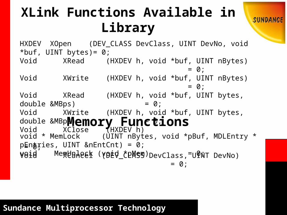
XLink Functions Available in Library
HXDEV XOpen (DEV_CLASS DevClass, UINT DevNo, void *buf, UINT bytes)= 0;Void XRead (HXDEV h, void *buf, UINT nBytes) = 0; Void XWrite (HXDEV h, void *buf, UINT nBytes) = 0; Void XRead (HXDEV h, void *buf, UINT bytes, double &MBps) = 0; Void XWrite (HXDEV h, void *buf, UINT bytes, double &MBps) = 0; Void XClose (HXDEV h) = 0;Void XCancel (DEV_CLASS DevClass, UINT DevNo) = 0;
Memory Functionsvoid * MemLock (UINT nBytes, void *pBuf, MDLEntry * pEntries, UINT &nEntCnt) = 0;void MemUnlock (void *pMem) = 0;
Sundance Multiprocessor Technology
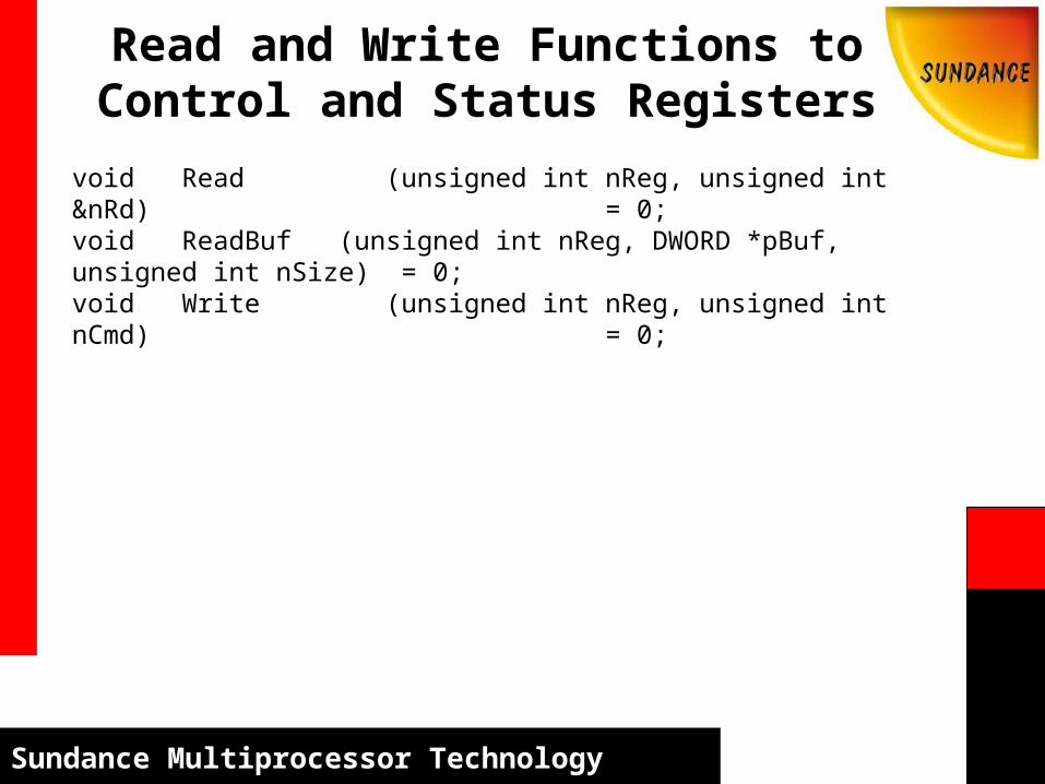
Read and Write Functions to Control and Status Registers
void Read (unsigned int nReg, unsigned int &nRd) = 0;void ReadBuf (unsigned int nReg, DWORD *pBuf, unsigned int nSize) = 0;void Write (unsigned int nReg, unsigned int nCmd) = 0;
Sundance Multiprocessor Technology
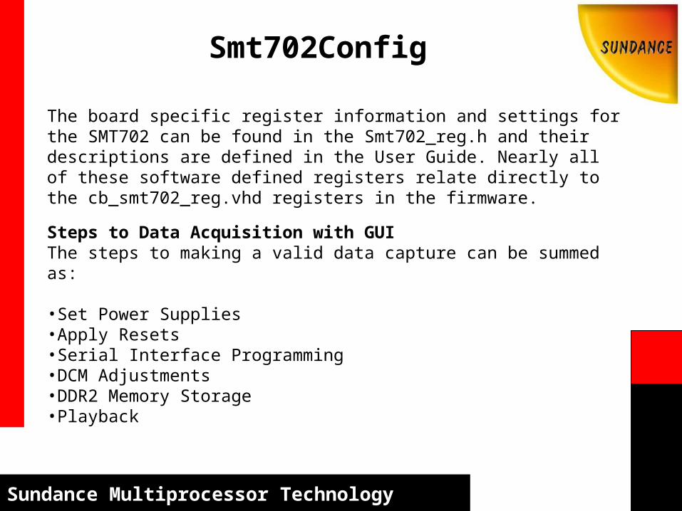
Smt702Config
The board specific register information and settings for the SMT702 can be found in the Smt702_reg.h and their descriptions are defined in the User Guide. Nearly all of these software defined registers relate directly to the cb_smt702_reg.vhd registers in the firmware.
Steps to Data Acquisition with GUIThe steps to making a valid data capture can be summed as:
•Set Power Supplies•Apply Resets•Serial Interface Programming•DCM Adjustments•DDR2 Memory Storage•Playback
Sundance Multiprocessor Technology
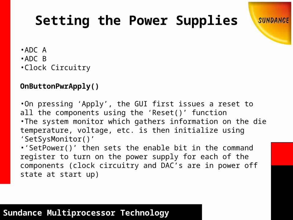
Setting the Power Supplies
•ADC A •ADC B•Clock Circuitry
OnButtonPwrApply()
•On pressing ‘Apply’, the GUI first issues a reset to all the components using the ‘Reset()’ function•The system monitor which gathers information on the die temperature, voltage, etc. is then initialize using ‘SetSysMonitor()’•‘SetPower()’ then sets the enable bit in the command register to turn on the power supply for each of the components (clock circuitry and DAC’s are in power off state at start up)
Sundance Multiprocessor Technology
Issuing Resets
ADCsDCM’sDDR2 Banks A and BSHB 1SHB 2
OnButtonRstApply()
•On pressing ‘Apply’, the GUI issues a reset to all the components above which are checked using the ‘Reset()’ function. These are not cleared automatically.

Sundance Multiprocessor Technology
Programming the Serial Interfaces•Reference Source•Clock Source•ADC A Configuration Register Programming•ADC B Configuration Register Programming•ADC’s Calibration
OnButtonIntApply()
•First the reference source bit is set using SetRefClk()•The default clock settings are then sent to the clock registers in the FPGA. Once these values have been verified in a read back, the values are then ‘updated’, meaning they are sent to the clock chip over a serial link. This is all accomplished with SetClkSrc()•Poll() is used to monitor the completion bit of this serial programming•The default ADC A settings are then sent to the ADC A registers in the FPGA. Once these values have been verified in a read back, the values are then updated and serial programmed also. This is all accomplished with SetADC()•Poll() is used to monitor the completion bit of this serial programming
Sundance Multiprocessor Technology
Programming the Serial Interfaces
•The default ADC B settings are then sent to the ADC B registers in the FPGA. Once these values have been verified in a read back, the values are then updated and serial programmed also. This is all accomplished with SetADC()•Poll() is used to monitor the completion bit of this serial programming•The next step is a calibration setting for the both of the ADC’s issued with SetCalibration()•Poll() is used to monitor the completion bit of this calibration•The final step is a reset issued to ADC A and B with Reset()
Sundance Multiprocessor Technology
DCM Shift Adjustments•ADC A Shift Adjustment(value)•ADC B shift Adjustment(value)
OnButtonShiftedadjApply()
•The first SetShiftAdj() is issued to initialize the DCM’s to a phase offset of 0. The completion of this is monitored using Poll()•A loop is then begun until the phase relationship between ADC A sampling clock and ADC B sampling clock are close enough in phase to be considered synchronized
• First a reset is sent to the ADC’s using Reset()• SetShiftAdj() is applied 128 times to cover a half period of the clock, ensuring
the clock edge recovery. Read() recovers the clock edge of each sampled phaseshift and XOR’s the result
• If the result is high, a counter is incremented. If the counter is too high (phase is too misaligned) the loop repeats
•Once the clock phases are close enough, a final SetShiftAdj() is issued to align the clock edge to data window correctly for data capture. The default value for a 3Gsps sampling clock is set already.

Sundance Multiprocessor Technology
Filling DDR2 Memory•Fill up DDR banks
OnButtonDDR2MemApply()
•First the DDR2 is issued a reset using Write(), then cleared using Write() again.•Poll() monitors all the initialization steps in the DDR of both banks to monitor when the memory is available for use•The DDR2 capture enable bit is set using Write()•A loop until is begun
• The FIFO A and FIFO B full flags are Read() until the memory is full, then the loop exits
•The capture enable bit for the DDR2 is then cleared with Write()
Sundance Multiprocessor Technology
Acquisitions•Save Capture Data to XX files per channel
OnButtonAcqStart()
•A thread is begun to read the memory contents (m_hStart)•A 2K buffer of memory is locked on the host using MemLock()•The number of bits stored in FIFO A is Read()•The number of bits stored in FIFO B is Read()•The buffer is then filled with 2K samples from FIFO A using CpRead(). These samples are masked and bit shifted to represent the separate samples (they arrive concatenated).•The temporary buffer is then stored to file (if selected) by using GetDatatoFile() first to store ADC A’s samples, then again to append the 2K samples to the last read 2K samples.•Samples from ADC A are then sent to the graphing functions
Sundance Multiprocessor Technology
Acquisitions
•The buffer is then filled with 2K samples from FIFO B using CpRead(). These samples are masked and bit shifted to represent the separate samples (they arrive concatenated).•The temporary buffer is then stored to file (if selected) by using GetDatatoFile() first to store ADC B’s samples, then again to append the 2K samples to the last read 2K samples.•Samples from ADC B are then sent to the graphing functions
The thread continues until ‘Stop’ is pressed (m_hStop) or the memory is emptied

Sundance Multiprocessor Technology
Smt712Config
The board specific register information and settings for the SMT712 can be found in the Smt712_reg.h and their descriptions are defined in the User Guide. Nearly all of these software defined registers relate directly to the cb_smt712_reg.vhd registers in the firmware.
Steps to Data Transmission with GUIThe steps to making a valid data transmission can be summed as:
•Set Power Supplies•Apply Appropriate Resets•Serial Interfaces•DCM Adjustments•Data Source Selection
Sundance Multiprocessor Technology
Setting the Power Supplies
•ADC A •ADC B•Clock Circuitry
OnButtonPwrApply()
•On pressing ‘Apply’, the GUI first issues a reset to all the components using the ‘Reset()’ function•The synchronization enable, reset, and synch start bit are then cleared with Write()•Power to the clock circuitry and DAC’s are then cycled off then on using PwrOff() and PwrOn(), if the options are checked.

Sundance Multiprocessor Technology
Issuing Resets
DACsClock CircuitryDDR2 Banks A and BSystem MonitorSHB 1SHB 2
OnButtonRstApply()
•On pressing ‘Apply’, the GUI enables the synchronization (does not send a reset) with SetDacSync().•A reset is then applied to all the check options with Reset()•The data source is selected for transmitting using the SetDataSrc() function
Sundance Multiprocessor Technology
Programming the Serial Interfaces•Reference Source•Clock Source•DAC A Configuration Register Programming•DAC B Configuration Register Programming•Synchronize DAC’s
OnButtonIntApply()
•First the reference source bit is set using SetRefClk()•The reset bit for the DAC’s is then cleared using Write()•The default DAC A settings are then sent to the DAC A registers in the FPGA. Once these values have been verified in a read back, the values are then updated and serial programmed. This is all accomplished with SetDAC()•The default DAC B settings are then sent to the DAC B registers in the FPGA. Once these values have been verified in a read back, the values are then updated and serial programmed also. This is all accomplished with SetDAC()•The reset for the clock circuitry is cleared using Write()

Sundance Multiprocessor Technology
Programming the Serial Interfaces
•The default clock settings are then sent to the clock registers in the FPGA and verified in a read back. This is all accomplished with SetClkSrc()•The clock register settings are then serial programmed to the clock chip with an update to the FPGA registers using UpdateClkReg()•After the clock chip is initialized, a calibration sequence setting for the VCO is sent to the FPGA with CalibrateVCO(). UpdateClkReg() is again used to update and send these serial configuration words to the clock chip.•Read() is used to determine when this calibration cycle is complete.•Synch() sends a low, then a high to the synchronization bit.•A reset is then sent to DCM A with Rst_DCMDAC(), then to DCM B
Sundance Multiprocessor Technology
Programming the Serial Interfaces
•If a synchronization of the DAC’s is checked –• The synch reset bit will be cleared with Write()• The first SetShiftAdj() is issued to initialize the DCM’s to a phase offset of 0. • A loop then begins –
• Write() sets the synchronization enable bit, then clears it• SetShiftAdj() is applied 255 times to cover a half period of the clock,
ensuring the clock edge recovery. The function returns the XOR’ed result of the clock edge of each sampled phaseshift
• If the result is high, a counter is incremented. If the counter is too high (phase is too misaligned) the loop repeats
Sundance Multiprocessor Technology
DCM Shift Adjustments
•DAC A Shift Adjustment(value)•DAC B shift Adjustment(value)
OnButtonShiftedadjApply()
•SetShiftAdj() is issued to align the clock to the correct window time for accurate latching of the data to the DAC. The default value is set to correctly work with the onboard clock circuitry

Sundance Multiprocessor Technology
Data Source Selection
•File (DDR2 Pattern Generator, both DAC A and B•DDR2 Pattern Generator (specify size of pattern, number of periods)•FPGA embedded DDS (specify phase increment)•SHB
If User File to DDR2 is Source~
•The specified file for A is scanned for the number of samples it holds with GetFileSize(), then the same is performed for channel B.•Write() sets the DDR2 reset, then clears the reset•The DDR2 is chosen as the source for DAC output with SetDataSrc()•The size of the pattern for DAC A is written with Write(), then the size of the pattern for B is written with Write()•The actual pattern in the file for channel A is scanned and written to the DDR2 A offset with SendPattern(). The same is again done for channel B.
First – Write() clears the start/stop bit for DDR2 enable
Sundance Multiprocessor Technology
Data Source Selection
If DDR2 Pattern Generator is Source~
•First Write() sets the DDR2 reset, then clears the reset•The DDR2 is chosen as the source for DAC output with SetDataSrc()•The size of the pattern for DAC A is written with Write(), then the size of the pattern for B is written with Write()•A sine wave is then generated in the Host with the size/number of periods specified. The pattern is sent to channel A DDR2 over XLink using CpWrite(), then channel B DDR2.
Sundance Multiprocessor Technology
Data Source Selection
If embedded DDS is Source~
•The DDS is chosen as the source for DAC output with SetDataSrc()•The phase increment variable is sent to the DDS for DAC A with Write(), then the phase increment is sent to the DDS for DAC B
If SHB is Source~
•No special configuration required - SHB input is simply chosen as the source for DAC output with SetDataSrc()
Sundance Multiprocessor Technology
Questions?