Embed Size (px)
Citation preview

MAHARASHTRA STATE BOARD OF TECHNICAL EDUCATION
(Autonomous)
(ISO/IEC - 27001 - 2005 Certified)
_____________________________________________________________________________________
1
SUMMER– 15 EXAMINATION
Subject Code: 17535 Model Answer
Important Instructions to examiners:
1) The answers should be examined by key words and not as word-to-word as given in the
model answer scheme.
2) The model answer and the answer written by candidate may vary but the examiner may try
to assess the understanding level of the candidate.
3) The language errors such as grammatical, spelling errors should not be given more
Importance (Not applicable for subject English and Communication Skills.
4) While assessing figures, examiner may give credit for principal components indicated in the
figure. The figures drawn by candidate and model answer may vary. The examiner may give
credit for any equivalent figure drawn.
5) Credits may be given step wise for numerical problems. In some cases, the assumed constant
values may vary and there may be some difference in the candidate‟s answers and model answer.
6) In case of some questions credit may be given by judgement on part of examiner of relevant
answer based on candidate‟s understanding.
7) For programming language papers, credit may be given to any other program based on
equivalent concept.

MAHARASHTRA STATE BOARD OF TECHNICAL EDUCATION
(Autonomous)
(ISO/IEC - 27001 - 2005 Certified)
_____________________________________________________________________________________
2
Q.1 a) Attempt any THREE 12 marks
1) Define Sampling theorem and state Nyquist Rate.
Ans: (Theorem – 2 marks, Nyquist Rate – 2 marks)
Theorem states that, „If the sampling rate in any pulse modulation system exceeds twice the
maximum signal frequency, the original signal can be reconstructed in the receiver with
minimum distortion.‟
Mathematically it is expressed as,
Where, fs = sampling frequency
fm = maximum frequency of continuous original signal.
Nyquist Rate:
The minimum sampling rate of „2fm‟ samples per second for a signal x (t) having maximum
frequency of „fm‟ Hz is called as Nyquist Rate.
2) List different types of errors and their causes.
Ans: (Types of errors – 2 marks, any two relevant causes of errors – 2 marks)
Types of errors (2 Marks) The errors introduced in the data bits during their transmission can be categorized as,
1. Content errors
2. Flow integrity errors
Depending on the number of bits in the error, the errors can be classified into two types as:
1. Single bit error
2. Burst error
Causes of errors: (any 2 relevant points- 2 Marks)
Due to addition of noise in transmission & reception of data following errors occur.
1. If data block is lost in the network as it has been delivered to wrong destination.
2. If two or more bits from data unit such as a byte change from 1 to 0 or 0 to 1.
3) State need of multiplexing in communication.
Ans: (Relevant correct answer – 4 marks)
Need of multiplexing:
In telephone systems, there are large numbers of users involved.
It is not possible to connect separate wires from each subscriber to all other subscribers.
It is very expensive and increases complexity.
Instead we can use a communication medium such as a coaxial cable or optical fiber cable to
carry many telephone signals from different sources together.
This can be achieved by „Multiplexing‟.

MAHARASHTRA STATE BOARD OF TECHNICAL EDUCATION
(Autonomous)
(ISO/IEC - 27001 - 2005 Certified)
_____________________________________________________________________________________
3
4) List advantages of Spread Spectrum (SS) modulation over other.
Ans: (Any four correct points – 1 mark each)
Advantages of Spread Spectrum Modulation are:
1. Low Power Density
2. Redundancy
3. Anti-jamming (A/J)
4. Anti-interference (A/I)
5. Low Probability of Intercept (LPI)
6. Message Privacy
7. High Resolution Ranging and Timing
Q.1 b) Attempt any ONE 6 marks
1) Draw the block diagram of digital communication system and explain in detail.
Ans: (Diagram – 3 marks, explanation – 3 marks)
(OR)
MAHARASHTRA STATE BOARD OF TECHNICAL EDUCATION
(Autonomous)
(ISO/IEC - 27001 - 2005 Certified)
_____________________________________________________________________________________
4
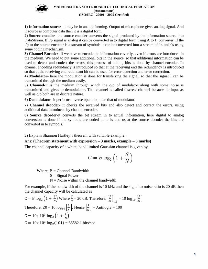
1) Information source- it may be in analog forming. Output of microphone gives analog signal. And
if source is computer data then it is a digital form.
2) Source encoder- the source encoder converts the signal produced by the information source into
DataStream. If i/p signal is analog it can be converted in to digital form using A to D converter. If the
i/p to the source encoder is a stream of symbols it can be converted into a stream of 1s and 0s using
some coding mechanism.
3) Channel Encoder- if we have to encode the information covertly, even if errors are introduced in
the medium. We need to put some additional bits in the source, so that additional information can be
used to detect and coolest the errors, this process of adding bits is done by channel encoder. In
channel encoding redundancy is introduced so that at the receiving end the redundancy is introduced
so that at the receiving end redundant bit can be used for error detection and error correction.
4) Modulator- here the modulation is done for transferring the signal, so that the signal I can be
transmitted through the medium easily.
5) Channel-it is the medium through winch the o/p of modulator along with some noise is
transmitted and gives to demodulator. This channel is called discrete channel because its input as
well as o/p both are in discrete nature.
6) Demodulator- it performs inverse operation than that of modulator.
7) Channel decoder- it checks the received bits and also detect and correct the errors, using
additional data introduced by channel encoder.
8) Source decoder-it converts the bit stream in to actual information, here digital to analog
conversion is done if the symbols are coded in to is and os at the source decoder the bits are
converted in to symbols.
2) Explain Shannon Hartley‟s theorem with suitable example.
Ans: (Theorem statement with expression – 3 marks, example – 3 marks)
The channel capacity of a white, band limited Gaussian channel is given by,
Where, B = Channel Bandwidth
S = Signal Power
N = Noise within the channel bandwidth
For example, if the bandwidth of the channel is 10 kHz and the signal to noise ratio is 20 dB then
the channel capacity will be calculated as
(
) Where
= 20 dB. Therefore, *
+
= 10 *
+
Therefore, = 10 *
+. Hence *
+ = Antilog 2 = 100
(
)
( ) = 66582.1 bits/sec

MAHARASHTRA STATE BOARD OF TECHNICAL EDUCATION
(Autonomous)
(ISO/IEC - 27001 - 2005 Certified)
_____________________________________________________________________________________
5
Q.2 Attempt any TWO 16 marks
1) Draw and explain PCM Transmitter and state any two advantages and two disadvantages.
Ans: (Transmitter diagram – 2 marks, explanation – 2 marks, any two advantages and
disadvantages – 2 mark each)
PCM Transmitter Diagram (2 Marks)
(OR)
PCM Transmitter Explanation (2 Marks)
The analog signal x (t) is passes through band limiting / low pass filter, which has a cut-off
frequency fc=W Hz. This will ensure x (t) will not have any frequency component higher
than “W”. In other words, suppresses high frequency components and passes only low
frequency signal to avoid „aliasing error‟.
The band limited analog signal is then applied to sample and circuit where this circuit acts as
modulator and both modulating input signal and sampling signal with adequately high
sampling rate are inputs to this circuit. Output sample and hold block is a flat topped PAM
signal.

MAHARASHTRA STATE BOARD OF TECHNICAL EDUCATION
(Autonomous)
(ISO/IEC - 27001 - 2005 Certified)
_____________________________________________________________________________________
6
These samples are subjected to operation “quantization” in the “quantizer”. The quantizer is
used to reduce effect of noise. Quantization is a process of approximation of the value of
respective sample in to a finite number that will reduce data bits. The combined effect of
sample and quantization produces is „Quantized PAM‟ at the quantizer output.
The Quantized PAM output is analog in nature. So to transmit it through digital
communication system the quantized PAM pulses are applied to an encoder which is
basically A to D convertor. Each quantized level is converted into N bit digital word by A to
D converter.
The communication system is normally connected to each other using a single cable i.e.
serial communication. But the output of ADC is parallel which cannot be transmitted through
serial communicating links. So this block will convert the parallel data into serial stream of
data bits.
A pulse generator produces train of rectangular pulses of duration “t” seconds. This signals
acts as sampling signals for the sample and hold block. The same signal acts as “clock”
signals for parallel to converter .the frequency “f” is adjusted to satisfy the criteria.
Advantages: (2 Marks)
1. PCM has very high noise immunity.
2. Repeaters can be used between the transmitter and the receiver which can further reduce
the effect of noise.
3. It is possible to store the PCM signal due to its digital nature.
4. It is possible to use various coding techniques so that only the desired receiver (user) can
decode the message.
Disadvantages: (2 Marks)
1. The encoding decoding & quantizing circuitry of PCM is complex.
2. PCM requires a large BW as compared to other systems.
2) List different digital modulation techniques and explain amplitude shift keying modulation in
detail.
Ans: (List of modulation – 3 marks, ASK block diagram – 2 marks, explanation – 2 marks,
waveform – 1 mark)
Amplitude Shift Keying (ASK) is the digital modulation technique in which the amplitude of the
sinusoidal carrier will take one of the two predetermined values in response to 0 or 1 value of the
digital input modulating message signal.

MAHARASHTRA STATE BOARD OF TECHNICAL EDUCATION
(Autonomous)
(ISO/IEC - 27001 - 2005 Certified)
_____________________________________________________________________________________
7
Explanation
Amplitude shift keying is the simplest form of digital modulation. Here the carrier is a sine
wave of frequency ( ). The carrier signal can be mathematically expressed as = sin (2π t) The digital signal from the information source is a unipolar NRZ signal which acts as the
modulating signal. The ASK modulator is nothing but a multiplier followed by a band pass
filter as shown in above figure.
Due to multiplication, the ASK output will be present only when a binary „1‟ is to be
transmitted and when the digital input is „0‟ then we get zero output as shown in the
waveform above.
From the waveform analysis we can conclude that when a binary „1‟ is to be sent the carrier
is transmitted and when binary „0‟ is to be sent then the carrier is not transmitted.
Mathematically ASK signal can be expressed as;
( ) sin (2π t)
Where d = data bit which can take values 1 or 0
Therefore, ( ) sin (2π t) When d = 1
( ) When d = 0
3) Draw and explain block diagram of Time Division Multiplexing (TDM) and state its
advantages (min. 4).
Ans: (TDM block diagram – 3 marks, explanation – 3 marks, any four advantages – 2
marks)
Diagram: TDM Block diagram

MAHARASHTRA STATE BOARD OF TECHNICAL EDUCATION
(Autonomous)
(ISO/IEC - 27001 - 2005 Certified)
_____________________________________________________________________________________
8
(OR)
Fig: TDM Transmitter
Fig: TDM Receiver
Note: TDM Transmitter or Receiver with explanation should be considered and given
marks. Any relevant diagram should be considered
Explanation
Process of combining digital signals from several sources whereby each connection occupies a
portion of time in the link is called Time Division Multiplexing (TDM).
Links are sectioned by time rather than frequency.
Data flow of each connection is divided into units.
In TDM data units from each input connection is collected in to a frame i.e link combines one unit
of each connection to make a frame.
If we have “n” connection a frame is divided in to “n” time slots and one slot is allowed for each unit.
i.e. n input connections n time slots.
One for each input line, if the duration of input is T, the duration of each slot is T/n and the duration
of each frame is T.
Data rate of link must be n times the duration of a time slot to guarantee flow of data.
Time slots are grouped into frames; one complete cycle of time slots; each slot dedicated to one
device.
A simple TDM process for three different data transmission is shown above.
Here, all three data are divided into equal timeslots also called as units.
And each data unit from all three data are combined / multiplexed together to form TDM frames comprising of small units of all three data which is further transmitted.

MAHARASHTRA STATE BOARD OF TECHNICAL EDUCATION
(Autonomous)
(ISO/IEC - 27001 - 2005 Certified)
_____________________________________________________________________________________
9
Q.3 Attempt any FOUR 16 marks
1) Explain basic working principle of code division multiple access technology.
Ans: (Diagram – 2marks, Explanation-2 marks)
Explanation:-
In CDMA more than one user is allowed to share a channel or sub channel with the help of DSSS
signals. In CDMA each user is given a unique code sequence. This sequence allows the user to
spread the information signal across the assigned frequency. At the receiver the signal received from
various users are separated by checking the cross correlation of the received signal with each possible
user sequence. In CDMA as the bandwidth as well as time of the channel is being shared by users. In
CDMA the users access the channel in a random manner. Hence the signals transmitted by multiple
users will overlap both in time and in frequency. CDMA does not need any synchronization.
(OR)
2) Draw the block diagram of DPSK transmitter and explain.
Ans: (Block diagram- 2 marks, explanation-2 marks)
In BPSK receiver, the carrier recovery is done by squaring the received signal.
Hence, when the received signal is generated by negative data bit, it is squared and thus we cannot
determine if the received bit is –b (t) or b (t) .Hence DPSK is used to eliminate the ambiguity of the
received bit. The DPSK transmitter is as shown -
(OR)

MAHARASHTRA STATE BOARD OF TECHNICAL EDUCATION
(Autonomous)
(ISO/IEC - 27001 - 2005 Certified)
_____________________________________________________________________________________
10
Explanation
1) d (t) represents the data stream which is to be transmitted it is to one input of an EX-OR logic
gate.
2) The EX-OR gate output „b (t)‟ is delayed by one bit period the applied to the other input of
EX-OR gate. The delayed represented by „b (t-Tb)‟.
3) Depending on the values of „d (t)‟ and „b (t-Tb)‟ the EX-OR produces the output sequence
„b (t)‟.the waveform for the generator .the waveform drawn by arbitrarily assuming that in the
first interval b (0) = 0.
4) Output of EX-OR gate is the applied to a bipolar NRZ level which converts „b(t)‟ to a bipolar
level “b(t) as shown
b(t) b”(t)
0 -1
1 +1
5) The o/p is given as-
VDpsk (t) = √ (2 Ps) cosωt
That Means no phase Shift has been introduced
But when b (t) = 0, b‟ (t) = -1 Hence
VDpsk (t) = √ (2 Ps) cosωt
Thus 180 Phase shift is introduced to represent b (t) =0.

MAHARASHTRA STATE BOARD OF TECHNICAL EDUCATION
(Autonomous)
(ISO/IEC - 27001 - 2005 Certified)
_____________________________________________________________________________________
11
3) State the necessity of adaptive delta modulation technique.
Ans: (Need with proper explanation -4 marks)
In delta modulation, the step size is constant so that its slope overload distortion and granular
noise both cannot be controlled. These drawbacks can be controlled by using adaptive delta
modulation wherein the step size is variable.
Thus with adaptive delta modulation the following are the advantages-
1. Slope overload distortion and granular noise problem in is reduced.
2. Improved signal to noise ratio.
3. Wide dynamic range is achieved with variable step size.
4. Better bandwidth utilization than delta modulation.
4) Compare digital pulse modulation with analog modulation.
Ans: (Any four relevant correct points – 1 mark each)
Sr.
No
Digital Pulse modulation Analog/Continuous wave modulation
1 The carrier is train of pulses. The carrier is sine wave
2 The modulation can be done by varying
width, position and amplitude of pulse.
The modulation can be done by varying the
amplitude, phase and frequency of the sine wave.
3 More bandwidth required Less bandwidth required.
4 Applications in Satellite communication,
communication between spaceships and
earth stations.
Applications in broadcasting radio and TV.
5 The noise immunity for PAM is least but
rest all modulation techniques work well.
The noise immunity is low for AM. While PM
and FM work well.
6 Digital modulation is possible. Digital Modulation is not possible.
7 Simpler and less costly. Costly and complicated
5) Explain M-ary encoding technique.
Ans: (Proper explanation with example- 4 marks)
In an M-ary signaling scheme, we can send one of the m possible signals such as s1, s2...sm (t) during
each signaling interval of duration of t seconds.
The number of signals in an M is given as M=2n.
The M-ary signals are obtained as follows.
Group of „N‟ bits together form N bit symbols.
These signals will extend over a period of NTb where tb is duration of one bit.
Due to grouping of n bit per symbols, we can have 2n =M possible symbols.
These M possible signals are represented by sinusoidal signals of duration Ts = NTb which differ
from one another by a phase of 2π/m radians .thus M-ary signal is produced at the output.

MAHARASHTRA STATE BOARD OF TECHNICAL EDUCATION
(Autonomous)
(ISO/IEC - 27001 - 2005 Certified)
_____________________________________________________________________________________
12
Example: QPSK
Value of M = 4 also called 4aryPSK.The number of bits in one symbol are = 2.
Hence there are 22 = 4 possible symbols.
Symbol1: 00
Symbol2: 01
Symbol3: 10
Symbol4: 11
Q.4 a) Attempt any THREE 12 marks
1) State historical perspective of digital communication.
Ans: (Relevant correct explanation – 4 marks)
Ever since human beings learnt to communicate, the goal is to send and to receive maximum
information over vast distances in shortest period of time. For communication, the information
signals that are mostly used are electrical in nature. The information is transmitted in the
electrical form i.e., in the form of electrical current or electrical voltage and at the receiving end,
the information is regenerated from its electrical outputs.
Even now, information signal can be optical in nature. Using optical mode, information can be
transmitted, received and stored as well. The development of optical fibre technology is the
milestone in the global telecommunications and information technology revolution. Besides
voice communication, to-days‟ telephone companies are serving their customers‟ ever expanding
demands like: Audio, video, fax and data transmission , Internet and multimedia services , e-
mail , Video conferencing , e-business, e-education, e-banking, e-medical services.
The optical information can be transmitted through optical fiber as optical fibre can guide light.
Apart from optical communication, optical fibers are being used in many different types of
applications including optical inspection/surgery, non-contact sensing, traffic signs, museum
illumination, etc.
History about Different Types of Communication-The basic components of a communication
technology are:
1) Transmitter of Information signal
2) Carrier of signal
3) Receiver of signal
Considering different types of communication, the broad types can be cited, like, Radio,
Television, and Satellite & optical communication.
2) List advantages and disadvantages of delta modulation techniques.
Ans: (2 advantages-2 marks, 2 disadvantages-2 marks)
Advantages-
1) Low signaling rate and low transmission channel bandwidth.
2) Transmitter and receiver are less costly.
Disadvantages-
1) Slope overload error present
2) Granular noise present.

MAHARASHTRA STATE BOARD OF TECHNICAL EDUCATION
(Autonomous)
(ISO/IEC - 27001 - 2005 Certified)
_____________________________________________________________________________________
13
3) Explain Alternate Mark inversion (AMI) coding with suitable example.
Ans: (Define- 1 mark, example with waveform—3 marks)
AMI- Alternate Mark Inversion- In this line coding a „0‟ is represented at zero level( 0V) while
alternate 1‟s are represented at 1V and -1V level as shown with an example-
AMI waveforms of line codes for data stream 1101001 is as shown-
4) List and explain different types of frequency hopping.
Ans: (List-1 marks, Explanation for both 1 ½ marks each)
Types of frequency hopping-
1) Slow frequency hopping
2) Fast frequency hopping
Slow frequency hopping-In slow frequency hopping the symbol rate Rs of the MFSK signal is
an integer multiple of the hop rate Rn that means several symbols are transmitted corresponding
to each frequency hop.
Each frequency hop: → several symbols
Here frequency hopping takes place slowly and thus
Hop rate Rh > Symbol rate Rs
Fast frequency hopping-In fast frequency hopping, multiple frequencies or hops are used to
transmit one symbol. That is each symbol-> several hops. So several frequencies changes for one
symbol such that Symbol rate Rs > Hop rate Rh.

MAHARASHTRA STATE BOARD OF TECHNICAL EDUCATION
(Autonomous)
(ISO/IEC - 27001 - 2005 Certified)
_____________________________________________________________________________________
14
Q.4 b) Attempt any ONE 6 marks
1) Generate CRC code for data word 110101011 the divisor is 01011.
Ans: (Code generation- 4 mks, generated CRC -1 mks, Final Coded data – 1 mark)
(Note - The divisor given is 01011, it should be taken as 1011 else it won’t be solved)
To generate the CRC code as divisor is 4 bit, add three zeros to the data and get the remainder as
shown below. The last three bit remainder is the required CRC send along with the data to be
transmitted.
The CRC Data is 1 1 1.
The final coded data transmitted will be 1 1 0 1 0 1 0 1 1 1 1 1
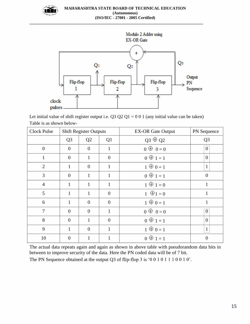
2) Explain PN sequence generation in detail.
Ans: (Any suitable diagram - 2 marks, explanation – 2 marks, generation table - 2 marks)
Note: Diagram & generation table with four flip-flops should also be considered
A PN sequence is defined as a pseudorandom coded sequence of 1s and 0s with certain auto
correlation properties.
Maximum length of PN Sequence „L‟ is the no. of bits in a PN sequence and it depends upon the
number of flip-flops „n‟ used for the PN Sequence generator and given as
L=2n
– 1
The block diagram for 3 bit that is 7 bit length of PN sequence generator is as shown with feedback
taps [3, 1]
MAHARASHTRA STATE BOARD OF TECHNICAL EDUCATION
(Autonomous)
(ISO/IEC - 27001 - 2005 Certified)
_____________________________________________________________________________________
15
Let initial value of shift register output i.e. Q3 Q2 Q1 = 0 0 1 (any initial value can be taken)
Table is as shown below-
Clock Pulse Shift Register Outputs EX-OR Gate Output PN Sequence
Q3 Q2 Q1 Q3 Q2 Q3
0 0 0 1 0 0 = 0 0
1 0 1 0 0 1 = 1 0
2 1 0 1 1 0 = 1 1
3 0 1 1 0 1 = 1 0
4 1 1 1 1 1 = 0 1
5 1 1 0 1 1 = 0 1
6 1 0 0 1 0 = 1 1
7 0 0 1 0 0 = 0 0
8 0 1 0 0 1 = 1 0
9 1 0 1 1 0 = 1 1
10 0 1 1 0 1 = 1 0
The actual data repeats again and again as shown in above table with pseudorandom data bits in
between to improve security of the data. Here the PN coded data will be of 7 bit.
The PN Sequence obtained at the output Q3 of flip-flop 3 is „0 0 1 0 1 1 1 0 0 1 0‟.

MAHARASHTRA STATE BOARD OF TECHNICAL EDUCATION
(Autonomous)
(ISO/IEC - 27001 - 2005 Certified)
_____________________________________________________________________________________
16
Q.5 Attempt any TWO 16 marks
1) Explain principle of frequency division multiplexing & compare FDM and CDM techniques.
Ans :- (Any relevant correct diagram – 2 mks, Explanation- 2 mks)
Principle of frequency division multiplexing
FDM means total range of frequency is divided into number of frequency slots. Each slots of
frequency is allotted to each channel. Various channels of different frequencies combined,
transmitted through single wire and separated at receiver with the help of De-multiplexer.
FDM can be applied when the bandwidth of the link is greater than the combined BW of the
signal to be transmitted. These modulated signals are than combined into a single composite
signal that can be transported by the links. Carrier frequency is separated by sufficient BW to
accommodate the modulated signal .These BW range are the channel through which the
various signals travels. Channels must be separated by guard bands to prevent signals from
overlapping.
Comparison of FDM & CDM techniques (Any 4 relevant points- 4 mks)
Sr.No FDM
CDM
1 Synchronization is not required. Synchronization is not necessary.
2 Overall bandwidth is shared among many
stations.
Sharing of bandwidth and time takes
place.
3 Due to non-linearity of devices inter
modulation products are generated due to
interference between adjacent channels.
Both type of interference will be present.
4 Code word is not required. Code words are required.
5 Guard bands between adjacent channels
are necessary.
Guard bands and guard times both are
necessary.

MAHARASHTRA STATE BOARD OF TECHNICAL EDUCATION
(Autonomous)
(ISO/IEC - 27001 - 2005 Certified)
_____________________________________________________________________________________
17
2) Draw block diagram of QAM generation system & Explain with waveforms.
Ans: (Any Relevant correct diagram – 4 mks, explanation- 2 mks, waveforms-2 mks)
Diagram: (4 marks)
Explanation: (2 marks) Figure shows transmitter for 4 bit QAM system. The input bit stream is applied to a serial to parallel
converter. Four successive bits are applied to the digital to analog converter. These bits are applied
after every Ts second. Ts is the symbol period & Ts=4Tb.Bits Bk & Bk+1 are applied to upper digital
to analog converter. & Bk+2, Bk+3 are applied to lower D to A converter. Depending upon the two
input bits, the output of D to A converter takes four output levels. Thus Ae (t) & Ao (t) takes 4 levels
depending upon the combination of two input bits. Ae (t) modulates the carrier cos (2πfct) and Ao (t)
modulates sin (2πfct).
The adder combines two signals to give QAM signal. It is given as,
S (t) = Ae (t) cos (2πfct) + Ao (t) sin (2πfct).
(OR)
Diagram: (4 marks)
MAHARASHTRA STATE BOARD OF TECHNICAL EDUCATION
(Autonomous)
(ISO/IEC - 27001 - 2005 Certified)
_____________________________________________________________________________________
18
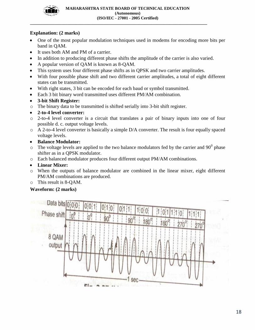
Explanation: (2 marks)
One of the most popular modulation techniques used in modems for encoding more bits per
band in QAM.
It uses both AM and PM of a carrier.
In addition to producing different phase shifts the amplitude of the carrier is also varied.
A popular version of QAM is known as 8-QAM.
This system uses four different phase shifts as in QPSK and two carrier amplitudes.
With four possible phase shift and two different carrier amplitudes, a total of eight different
states can be transmitted.
With right states, 3 bit can be encoded for each baud or symbol transmitted.
Each 3 bit binary word transmitted uses different PM/AM combination.
3-bit Shift Register:
o The binary data to be transmitted is shifted serially into 3-bit shift register.
2-to-4 level converter: o 2-to-4 level converter is a circuit that translates a pair of binary inputs into one of four
possible d. c. output voltage levels.
o A 2-to-4 level converter is basically a simple D/A converter. The result is four equally spaced
voltage levels.
Balance Modulator:
o The voltage levels are applied to the two balance modulators fed by the carrier and 900 phase
shifter as in a QPSK modulator.
o Each balanced modulator produces four different output PM/AM combinations.
Linear Mixer:
o When the outputs of balance modulator are combined in the linear mixer, eight different
PM/AM combinations are produced.
o This result is 8-QAM.
Waveform: (2 marks)

MAHARASHTRA STATE BOARD OF TECHNICAL EDUCATION
(Autonomous)
(ISO/IEC - 27001 - 2005 Certified)
_____________________________________________________________________________________
19
3) Describe the direct sequence spread spectrum techniques with the help of block diagram.
State advantages also.
Ans: (Diagram - 4 marks, explanation- 2 marks, advantages -2 marks (any two))
Note: DSSS receiver with explanation also should be considered and marks to be given
Direct sequence spread spectrum (DSSS):
In direct sequence, the serial binary data is mixed with a higher frequency pseudorandom binary
code at a faster rate and the result is used to phase-modulate a carrier.
DSSS Transmitter:
Explanation:
A block diagram of DS transmitter is shown in figure
The serial binary data is applied to an X- OR gate along with a serial pseudorandom code
that occurs faster than binary data.
The signal developed at the output of the X-OR gate is then applied to a BPSK modulator.
The carrier phase is switched between 00 and 180
0 by the 1‟s and 0‟s of X –OR output.
The signal phase modulating carrier, being much higher in frequency than the data signal
causes the modulator to produce multiple widely spaced sidebands whose strength is such
that the complete signal takes up a great deal of the spectrum. Thus the signal is spread.
Also because of its randomness, the resulting signal is appears to be nothing more than
wideband noise to a conventional narrow band receiver.
One bit time for the pseudorandom code is called a chip and the rate of the code is called the
chipping rate.
The chipping rate is faster than the data rate.
(OR)

MAHARASHTRA STATE BOARD OF TECHNICAL EDUCATION
(Autonomous)
(ISO/IEC - 27001 - 2005 Certified)
_____________________________________________________________________________________
20
The averaging system reduces the interference by averaging at over a long period. The DSSS system
is a averaging system. This technique can be used in practice for transmission of signal over a band
pass channel (E.g. satellite channel). For such application the coherent binary phase shift (BPSK) is
used in the transmitter and receiver.
The binary sequence b (t) is given to the NRZ encoder. The b (t) is converted NRZ signal d (t). The
NRZ signal d (t) is used to modulate the PN sequence c (t) generated by the PN code generator.
The multiplier multiply the signal b (t) * c (t) = s (t). The s (t) signal is given to binary PSK
modulator.
The modulated signal at the output of product modulator or multiplier i.e. s (t) is used modulate the
carrier for BPSK modulation.
The transmitted signal x (t) is thus DSSS signal.
Product modulator output = s (t)
s (t) = d (t) * c (t)
The BPSK carrier signal is given by √2Ps sin 2πfC t.
The output of BPSK modulator x (t) is transmitted x (t) = s (t) * √ 2Ps 2πfCt.
But m (t) = ± 1
Therefore x (t) = ± √2Ps sin2πfC t
The phase shift of x (t) of x (t) is 00 to + m (t) at is 1800 corresponding to a negative m (t).
Advantages of Spread Spectrum (SS): (any two)
1. Unauthorized listening is prevented.
2. SS signals are highly resistant to the jamming.
3. Unintentional interference occupying the same band is greatly minimized and in most cases
virtually eliminated.
4. Many users can share a signal band with no interference.
5. With SS, more signals can use a band than with any other type of modulation and
multiplexing.
6. Resistant to fading.
7. The pseudorandom code makes it possible to accurately determine the start and end of a
transmission.
8. Superior method for radar.

MAHARASHTRA STATE BOARD OF TECHNICAL EDUCATION
(Autonomous)
(ISO/IEC - 27001 - 2005 Certified)
_____________________________________________________________________________________
21
Q.6 Attempt any FOUR 16 marks
1) Explain Slope overload & Granular noise with respect to delta modulation.
Ans: (Graph – 2 marks, explanation of above two parameters – 1 mark each)
The delta modulation has two major drawbacks as under:
(i) Slope overload distortion
This distortion is arises because of large dynamic range of the input signal. As can be observed
from figure the rate of rise of input signal x(t) is so high that the staircase signal cannot
approximate it, the steep size „Δ‟ becomes too small for staircase signal x‟(t)to follow the step
segment of x(t). Hence, there is a large error between the staircase approximated signal and the
original input signal x (t). This error or noise is known as slope overload distortion. To reduce
this error, the step size must be increased when slope of signal x (t) is high. Since the step size of
delta modulator remains fixed, its maximum or minimum slopes occur along straight lines.
Therefore, this modulator is also known as Linear Delta Modulator (LDM).
(ii) Granular or Idle Noise:
Granular or Idle noise occurs when the step size is too large compared to small variations in the
input signal. This means that for very small variations in the input signal, the staircase signal is
changed by large amount (Δ) because of large step size figure shows that when the input signal is
almost flat, the staircase signal x‟(t) keeps on oscillating by ±Δ around the signal. The error
between the input and approximated signal is called granular noise. The solution to this problem
is to make step size small.
Therefore, a large step size is required to accommodate wide dynamic range of the input signal
(to reduce slope overload distortion) and small steps are required to reduce granular noise.
In fact, Adaptive delta modulation is the modification to overcome these errors.

MAHARASHTRA STATE BOARD OF TECHNICAL EDUCATION
(Autonomous)
(ISO/IEC - 27001 - 2005 Certified)
_____________________________________________________________________________________
22
2) Draw RZ, NRZ Manchester & Differential Manchester line code waveform for data stream
10100110.
Ans: (Correct waveforms – 1 mark each)
Note: RZ and NRZ both Unipolar or Polar or Bipolar waveform should be considered
MAHARASHTRA STATE BOARD OF TECHNICAL EDUCATION
(Autonomous)
(ISO/IEC - 27001 - 2005 Certified)
_____________________________________________________________________________________
23
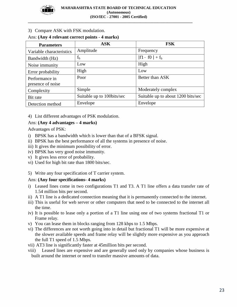
3) Compare ASK with FSK modulation.
Ans: (Any 4 relevant correct points - 4 marks)
Parameters ASK FSK
Variable characteristics Amplitude Frequency
Bandwidth (Hz) fb | | + fb
Noise immunity Low High
Error probability High Low
Performance in
presence of noise
Poor Better than ASK
Complexity Simple Moderately complex
Bit rate Suitable up to 100bits/sec Suitable up to about 1200 bits/sec
Detection method Envelope Envelope
4) List different advantages of PSK modulation.
Ans: (Any 4 advantages – 4 marks)
Advantages of PSK:
i) BPSK has a bandwidth which is lower than that of a BFSK signal.
ii) BPSK has the best performance of all the systems in presence of noise.
iii) It gives the minimum possibility of error.
iv) BPSK has very good noise immunity.
v) It gives less error of probability.
vi) Used for high bit rate than 1800 bits/sec.
5) Write any four specification of T carrier system.
Ans: (Any four specifications- 4 marks)
i) Leased lines come in two configurations T1 and T3. A T1 line offers a data transfer rate of
1.54 million bits per second.
ii) A T1 line is a dedicated connection meaning that it is permanently connected to the internet.
iii) This is useful for web server or other computers that need to be connected to the internet all
the time.
iv) It is possible to lease only a portion of a T1 line using one of two systems fractional T1 or
Frame relay.
v) You can lease them in blocks ranging from 128 kbps to 1.5 Mbps.
vi) The differences are not worth going into in detail but fractional T1 will be more expensive at
the slower available speeds and frame relay will be slightly more expensive as you approach
the full T1 speed of 1.5 Mbps.
vii) AT3 line is significantly faster at 45million bits per second.
viii) Leased lines are expensive and are generally used only by companies whose business is
built around the internet or need to transfer massive amounts of data.