Embed Size (px)
Citation preview
Rev C ©2009 Finisar Corporation AN-2035 Page 1 of 90 February 2009
1
Application Note AN-2035 2
Digital Diagnostic Monitoring Interface for XFP Optical Transceivers 3
4
SUMMARY OF CONTENTS 5
6
TITLE PAGE 7
8
9
Introduction to XFP Digital Diagnostics 2 10
11
XFP Product Portfolio and Part Number Designations 4 12
13
FTLX-1411M3 MEMORY MAP 7 14
15
FTLX1412M3 MEMORY MAP 16 16
17
FTLX-1611M3 MEMORY MAP 25 18
19
FTLX-1811M3 MEMORY MAP 33 20
21
FTLX-3811-3 MEMORY MAP 40 22
23
FTLX-3812-M3 MEMORY MAP 47 24
25
FTLX-3812-S3 MEMORY MAP 54 26
27
FTLX-8511D3 MEMORY MAP 68 28
29
FTLX4213 MEMORY MAP 79 30
31
32
33
34
35
36
37
38
39
40
41
42
43
Rev C ©2009 Finisar Corporation AN-2035 Page 2 of 90 February 2009
Overview 1
This Application Note defines Finisar implementation of the XFP 2-wire serial interface, 2
which is used for serial ID, digital diagnostics, and certain control functions. The 2-wire 3
serial interface is mandatory for all XFP modules and it is defined in the XFP MSA 4
Specification Rev 4.5. It is modeled largely after the digital diagnostics monitoring 5
interface proposed for the SFP and GBIC optical transceivers and defined in the SFF 6
draft document SFF-8472 Rev 10.1, which in turn is an extension of the original serial 7
ID systems defined for the GBIC and SFP transceivers. One major difference, however, 8
is that the memory structure is changed to use a single 2-wire interface address. 9
10
IMPORTANT: The digital diagnostics functionality and memory maps described in this 11
document apply to Beta-and Production-level units only. Please contact Finisar for 12
information on Alpha-level units. 13
14
As with GBIC and SFP transceivers, the XFP serial interface uses the 2-wire serial 15
CMOS EEPROM protocol defined for the ATMEL AT24C01A/02/04 family of 16
components. When the serial protocol is activated, the host generates the serial clock 17
signal (SCL pin). The positive edge clocks data into those segments of the memory map 18
that are not write-protected within the XFP transceiver. The negative edge clocks data 19
from the XFP transceiver. The serial data signal (SDA pin) is bi-directional for serial 20
data transfer. The host uses SDA in conjunction with SCL to mark the start and end of 21
serial protocol activation. The memories are organized as a series of 8-bit data words 22
that can be addressed individually or sequentially. The 2-wire serial interface provides 23
sequential or random access to 8 bit parameters, addressed from 0000h to the 24
maximum address of the memory. 25
26
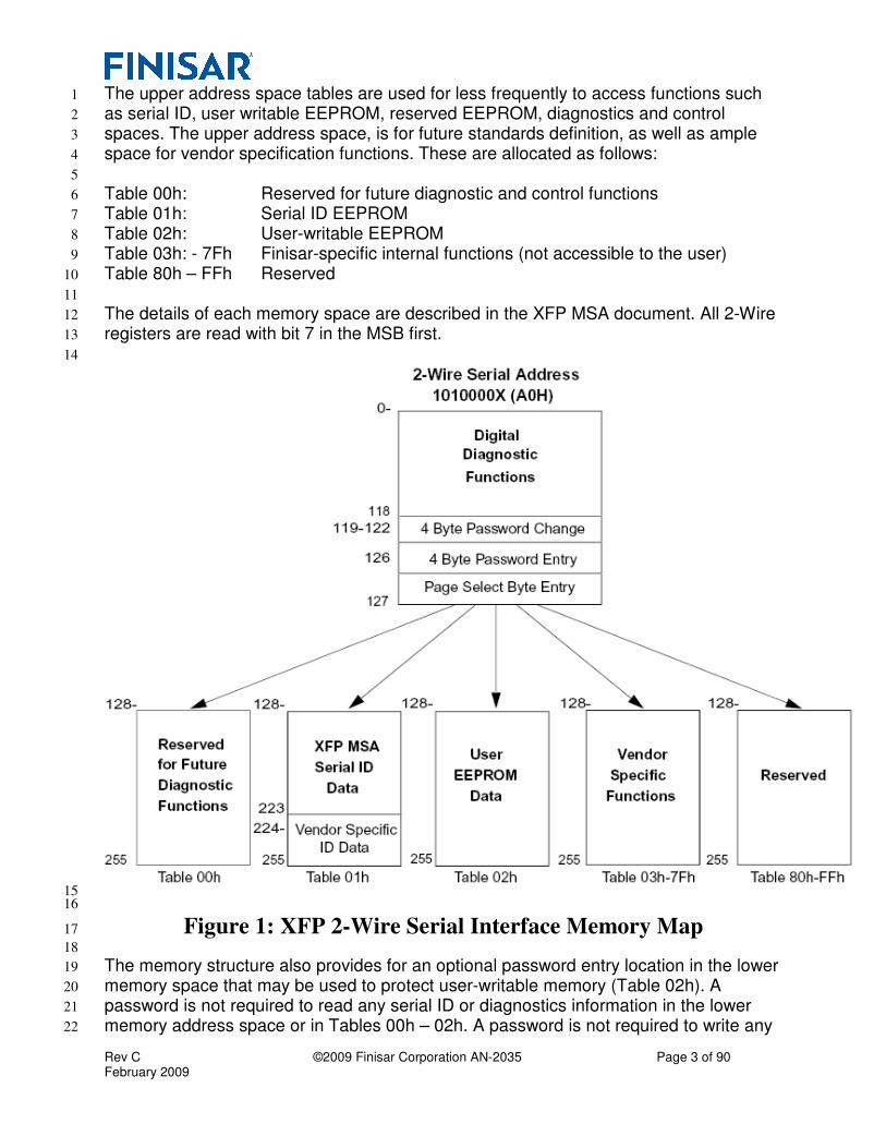
The structure of the memory map is shown in Figure 1. The normal 256-byte I2C 27
address space is divided into lower and upper blocks of 128 Bytes. The lower block of 28
128 bytes is always directly available and is used for the diagnostics and control 29
functions described in this document that must be accessed repeatedly. One exception 30
to this is that the standard module identifier byte defined in the GBIC and SFP 31
transceivers is located in Byte 0 of the memory map (in the diagnostics space) to allow 32
software developed for multiple module types to have a common branching decision 33
point. This byte is repeated in the serial ID section so that it also appears in the 34
expected relationship to other serial ID bits. 35
36
Multiple blocks of memories are available in the upper 128 Bytes of the address space. 37
These are individually addressed through a table select Byte which the user enters into 38
a location in the lower address space. Thus, there is a total available address space of 39
128 * 256 = 32 Kbytes in this upper memory space. 40
41
42
43
44
45
46
47
Rev C ©2009 Finisar Corporation AN-2035 Page 3 of 90 February 2009
The upper address space tables are used for less frequently to access functions such 1
as serial ID, user writable EEPROM, reserved EEPROM, diagnostics and control 2
spaces. The upper address space, is for future standards definition, as well as ample 3
space for vendor specification functions. These are allocated as follows: 4
5
Table 00h: Reserved for future diagnostic and control functions 6
Table 01h: Serial ID EEPROM 7
Table 02h: User-writable EEPROM 8
Table 03h: - 7Fh Finisar-specific internal functions (not accessible to the user) 9
Table 80h – FFh Reserved 10
11
The details of each memory space are described in the XFP MSA document. All 2-Wire 12
registers are read with bit 7 in the MSB first. 13
14
15 16
Figure 1: XFP 2-Wire Serial Interface Memory Map 17
18
The memory structure also provides for an optional password entry location in the lower 19
memory space that may be used to protect user-writable memory (Table 02h). A 20
password is not required to read any serial ID or diagnostics information in the lower 21
memory address space or in Tables 00h – 02h. A password is not required to write any 22
Rev C ©2009 Finisar Corporation AN-2035 Page 4 of 90 February 2009
controls defined in the digital diagnostic functions described in the MSA document 1
either. A password (entered into bytes 123 – 126) is required to allow write access to 2
the User EEPROM Table (02h). The default password is 00001011h per the XFP MSA, 3
and it can be changed by the host manufacturer by writing the new password into bytes 4
119 – 122 when the correct old password has been written into bytes 123 – 126. The 5
host password must be in the range of 00000000h to 7FFFFFFFh. 6
7
The 2-wire serial interface address of the XFP module is 1010000X (A0h). In order to 8
allow access to multiple XFP modules on the same 2-wire serial bus, the XFP pin-out 9
includes a MOD_DESEL or module deselect pin. This pin (which is pulled high or 10
deselected in the module) must be held low by the host to select the module of interest 11
and allow communication over the 2-wire serial interface. The module does not respond 12
to or accept 2-wire serial bus instructions unless it is selected. 13
14
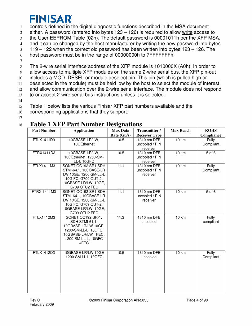
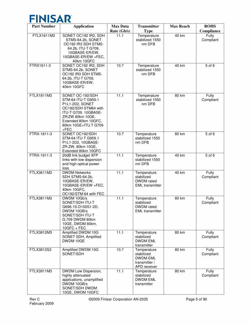
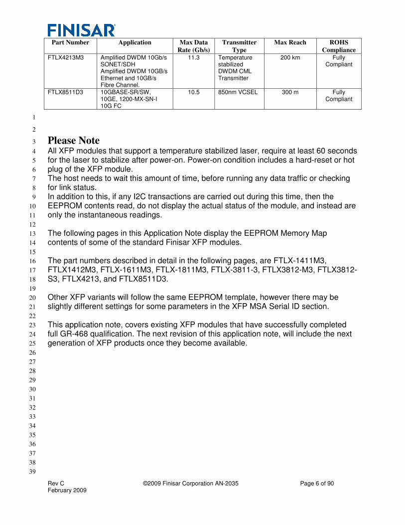
Table 1 below lists the various Finisar XFP part numbers available and the 15
corresponding applications that they support. 16
17
Table 1 XFP Part Number Designations 18
Part Number Application Max Data
Rate (Gb/s)
Transmitter /
Receiver Type
Max Reach ROHS
Compliance FTLX1411D3 10GBASE-LR/LW,
10GEthernet 10.5 1310 nm DFB
uncooled / PIN receiver
10 km Fully Compliant
FTRX1411D3 10GBASE-LR/LW, 10GEthernet ,1200-SM-
LL-L 10GFC
10.5 1310 nm DFB uncooled / PIN
receiver
10 km 5 of 6
FTLX1411M3 SONET OC192 SR1 SDH STMI-64.1, 10GBASE-LR LW 10GE, 1200-SM-LL-L
10G FC, G709 OUT-2, 10GBASE-LR/LW, 10GE,
G709 OTU2 FEC
11.1 1310 nm DFB uncooled / PIN
receiver
10 km Fully Compliant
FTRX-1411M3 SONET OC192 SR1 SDH STMI-64.1, 10GBASE-LR LW 10GE, 1200-SM-LL-L
10G FC, G709 OUT-2, 10GBASE-LR/LW, 10GE,
G709 OTU2 FEC
11.1 1310 nm DFB uncooled / PIN
receiver
10 km 5 of 6
FTLX1412M3 SONET OC192 SR-1, SDH STMI-61.1,
10GBASE-LR/LW 10GE, 1200-SM-LL-L, 10GFC,
10GBASE-LR/LW +FEC, 1200-SM-LL-L, 10GFC
+FEC
11.3 1310 nm DFB uncooled
10 km Fully compliant
FTLX1412D3 10GBASE-LR/LW 10GE 1200-SM-LL-L 10GFC
10.5 1310 nm DFB uncooled
10 km Fully Compliant
Rev C ©2009 Finisar Corporation AN-2035 Page 5 of 90 February 2009
Part Number Application Max Data
Rate (Gb/s)
Transmitter
Type
Max Reach ROHS
Compliance FTLX1611M3 SONET OC192 IR2, SDH
STMS-64.2b, SONET OC192 IR3 SDH STMS-
64.2b, ITU-T G709, 10GBASE-ER/EW,
10GBASE-ER/EW +FEC, 40km 10GFC
11.1 Temperature stabilized 1550
nm DFB
40 km Fully Compliant
FTRX1611-3 SONET OC192 IR2, SDH STMS-64.2b, SONET OC192 IR3 SDH STMS-64.2b, ITU-T G709, 10GBASE-ER/EW, 40km 10GFC
10.7 Temperature stabilized 1550
nm DFB
40 km 5 of 6
FTLX1811M3 SONET OC-192/SDH STM-64 ITU-T G959.1 P1L1-2D2, SONET OC192/SDH STM64 with ITU-T G709. 10GBASE-ZR/ZW 80km 10GE. Extended 80km 10GFC, 80km 10GE+ITU.T G709 +FEC
11.1 Temperature stabilized 1550
nm DFB
80 km Fully Compliant
FTRX-1811-3 SONET OC192/SDH STM-64 ITU-T G959.1 P1L1-2D2, 10GBASE-ZR-ZW, 80km 10GE, Extended 80km 10GFC
10.7 Temperature stabilized 1550 nm DFB
80 km 5 of 6
FTRX-1911-3 20dB link budget XFP links with low dispersion and high optical power loss
11.1 Temperature stabilized 1550 nm DFB
40 km 5 of 6
FTLX3611M3 DWDM Networks SDH STMS-64.2b, 10GBASE-ER/EW, 10GBASE-ER/EW +FEC, 40km 10GFC, OC192/STM-64 with FEC
11.1 Temperature stabilized DWDM rated EML transmitter
40 km Fully Compliant
FTLX3811M3 DWDM 10Gb/s SONET/SDH ITU-T G698.1S-D100S1-2D, DWDM 10GB/s SONET/SDH ITU-T G.709 DWDM 80km 10GE, DWDM 80km, 10GFC + FEC
11.1 Temperature stabilized DWDM rated EML transmitter
80 km Fully Compliant
FTLX3812M3 Amplified DWDM 10G SONET SDH, Amplified DWDM 10GE
11.1 Temperature stabilized DWDM EML transmitter
80 km Fully Compliant
FTLX3812S3 Amplified DWDM 10G SONET/SDH
10.7 Temperature stabilized DWDM EML transmitter / APD receiver
80 km Fully Compliant
FTLX3911M3 DWDM Low Dispersion, highly attenuated applications, unamplified DWDM 10GB/s SONET/SDH DWDM 10GE, DWDM 10GFC
11.1 Temperature stabilized DWDM EML transmitter
80 km Fully Compliant
Rev C ©2009 Finisar Corporation AN-2035 Page 6 of 90 February 2009
Part Number Application Max Data
Rate (Gb/s)
Transmitter
Type
Max Reach ROHS
Compliance FTLX4213M3 Amplified DWDM 10Gb/s
SONET/SDH Amplified DWDM 10GB/s Ethernet and 10GB/s Fibre Channel.
11.3 Temperature stabilized DWDM CML Transmitter
200 km Fully Compliant
FTLX8511D3 10GBASE-SR/SW, 10GE, 1200-MX-SN-I 10G FC
10.5 850nm VCSEL 300 m Fully Compliant
1
2
Please Note 3
All XFP modules that support a temperature stabilized laser, require at least 60 seconds 4
for the laser to stabilize after power-on. Power-on condition includes a hard-reset or hot 5
plug of the XFP module. 6
The host needs to wait this amount of time, before running any data traffic or checking 7
for link status. 8
In addition to this, if any I2C transactions are carried out during this time, then the 9
EEPROM contents read, do not display the actual status of the module, and instead are 10
only the instantaneous readings. 11
12
The following pages in this Application Note display the EEPROM Memory Map 13
contents of some of the standard Finisar XFP modules. 14
15
The part numbers described in detail in the following pages, are FTLX-1411M3, 16
FTLX1412M3, FTLX-1611M3, FTLX-1811M3, FTLX-3811-3, FTLX3812-M3, FTLX3812-17
S3, FTLX4213, and FTLX8511D3. 18
19
Other XFP variants will follow the same EEPROM template, however there may be 20
slightly different settings for some parameters in the XFP MSA Serial ID section. 21
22
This application note, covers existing XFP modules that have successfully completed 23
full GR-468 qualification. The next revision of this application note, will include the next 24
generation of XFP products once they become available. 25
26
27
28
29
30
31
32
33
34
35
36
37
38
39
Rev C ©2009 Finisar Corporation AN-2035 Page 7 of 90 February 2009
1
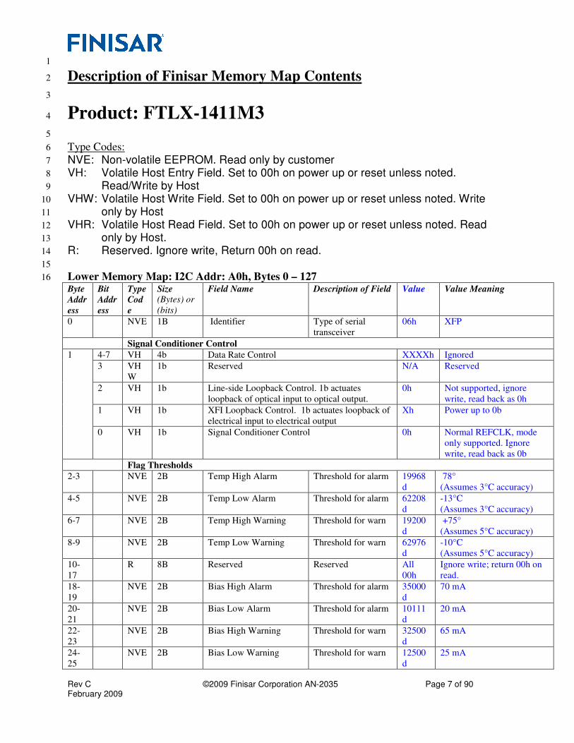
Description of Finisar Memory Map Contents 2
3
Product: FTLX-1411M3 4
5
Type Codes: 6
NVE: Non-volatile EEPROM. Read only by customer 7
VH: Volatile Host Entry Field. Set to 00h on power up or reset unless noted. 8
Read/Write by Host 9
VHW: Volatile Host Write Field. Set to 00h on power up or reset unless noted. Write 10
only by Host 11
VHR: Volatile Host Read Field. Set to 00h on power up or reset unless noted. Read 12
only by Host. 13
R: Reserved. Ignore write, Return 00h on read. 14
15
Lower Memory Map: I2C Addr: A0h, Bytes 0 – 127 16
Byte
Addr
ess
Bit
Addr
ess
Type
Cod
e
Size (Bytes) or
(bits)
Field Name Description of Field Value Value Meaning
0 NVE 1B Identifier Type of serial
transceiver
06h XFP
Signal Conditioner Control
1 4-7 VH 4b Data Rate Control XXXXh Ignored
3 VH
W
1b Reserved N/A Reserved
2 VH 1b Line-side Loopback Control. 1b actuates
loopback of optical input to optical output.
0h Not supported, ignore
write, read back as 0h
1 VH 1b XFI Loopback Control. 1b actuates loopback of
electrical input to electrical output
Xh Power up to 0b
0 VH 1b Signal Conditioner Control 0h Normal REFCLK, mode
only supported. Ignore
write, read back as 0b
Flag Thresholds
2-3 NVE 2B Temp High Alarm Threshold for alarm 19968
d
78°
(Assumes 3°C accuracy)
4-5 NVE 2B Temp Low Alarm Threshold for alarm 62208
d
-13°C
(Assumes 3°C accuracy)
6-7 NVE 2B Temp High Warning Threshold for warn 19200
d
+75°
(Assumes 5°C accuracy)
8-9 NVE 2B Temp Low Warning Threshold for warn 62976
d
-10°C
(Assumes 5°C accuracy)
10-
17
R 8B Reserved Reserved All
00h
Ignore write; return 00h on
read.
18-
19
NVE 2B Bias High Alarm Threshold for alarm 35000
d
70 mA
20-
21
NVE 2B Bias Low Alarm Threshold for alarm 10111
d
20 mA
22-
23
NVE 2B Bias High Warning Threshold for warn 32500
d
65 mA
24-
25
NVE 2B Bias Low Warning Threshold for warn 12500
d
25 mA
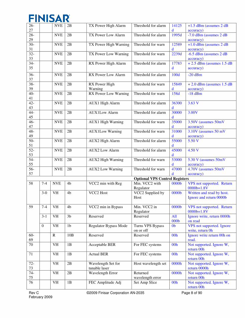
Rev C ©2009 Finisar Corporation AN-2035 Page 8 of 90 February 2009
26-
27
NVE 2B TX Power High Alarm Threshold for alarm 14125
d
+1.5 dBm (assumes 2 dB
accuracy)
28-
29
NVE 2B TX Power Low Alarm Threshold for alarm 1995d -7.0 dBm (assumes 2 dB
accuracy)
30-
31
NVE 2B TX Power High Warning Threshold for warn 12589
d
+1.0 dBm (assumes 2 dB
accuracy)
32-
33
NVE 2B TX Power Low Warning Threshold for warn 2239d -6.5 dBm (assumes 2 dB
accuracy)
34-
35
NVE 2B RX Power High Alarm Threshold for alarm 17783
d
+ 2.5 dBm (assumes 1.5 dB
accuracy)
36-
37
NVE 2B RX Power Low Alarm Threshold for alarm 100d -20 dBm
38-
39
NVE 2B RX Power High
Warning
Threshold for warn 15849
d
+ 2.0 dBm (assumes 1.5 dB
accuracy)
40-
41
NVE 2B RX Power Low Warning Threshold for warn 158d -18 dBm
42-
43
NVE 2B AUX1 High Alarm Threshold for alarm 36300
d
3.63 V
44-
45
NVE 2B AUX1Low Alarm Threshold for alarm 30000
d
3.00V
46-
47
NVE 2B AUX1 High Warning Threshold for warn 35000
d
3.50V (assumes 50mV
accuracy)
48-
49
NVE 2B AUX1Low Warning Threshold for warn 31000
d
3.10V (assumes 50 mV
accuracy)
50-
51
NVE 2B AUX2 High Alarm Threshold for alarm 55000
d
5.50 V
52-
53
NVE 2B AUX2 Low Alarm Threshold for alarm 45000
d
4.50 V
54-
55
NVE 2B AUX2 High Warning Threshold for warn 53000
d
5.30 V (assumes 50mV
accuracy)
56-
57
NVE 2B AUX2 Low Warning Threshold for warn 47000
d
4.70V (assumes 50mV
accuracy)
Optional VPS Control Registers
58 7-4 NVE 4b VCC2 min with Reg Min. VCC2 with
Regulator
0000b VPS not supported. Return
0000b=1.8V
3-0 VH 4b VCC2 Host VCC2 Supplied by
Host
0000b Written and read by host.
Ignore and return 0000b
59 7-4 VH 4b VCC2 min in Bypass Min. VCC2 in
Regulator
0000b VPS not supported. Return
0000b=1.8V
3-1 VH 3b Reserved Reserved All
000b
Ignore write, return 0000h
on read
0 VH 1b Regulator Bypass Mode Turns VPS Bypass
on or off
0b VPS not supported. Ignore
write, return 0h
60-
69
R 10B Reserved Reserved 00h Ignore write return 00h on
read.
70 VH 1B Acceptable BER For FEC systems 00h Not supported. Ignore W,
return 00h
71 VH 1B Actual BER For FEC systems 00h Not supported. Ignore W,
return 00h
72-
73
VH 2B Wavelength Set for
tunable laser
Host wavelength set 0000h Not supported. Ignore W,
return 0000h
74-
75
VH 2B Wavelength Error Returned
wavelength error
0000h Not supported. Ignore W,
return 00h
76 VH 1B FEC Amplitude Adj Set Amp Slice 00h Not supported. Ignore W,
return 00h
Rev C ©2009 Finisar Corporation AN-2035 Page 9 of 90 February 2009
77 VH 1B FEC Phase Adj Set Phase Slice 00h Not supported. Ignore W,
return 00h
78-
79
R 2B Reserved Reserved 00h Ignore write: return 00h on
read
80-
87
VHR 8B Latched Interrupt Flag
Bits
Individual bits set
per XFPMSA
xb Latched on flag condition.
Cleared on host read. (See
MSA)
88-
95
VH 8B Interrupt Masking Bits Individual bits set
per XFPMSA
0b Set and readable by host.
Cleared at power-up or
reset.
96-
97
VHR 2B Temperature Readout MSB in First Byte xxxxh Reported Temperature
Value in Units Defined in
XFP MSA 4.0
98-
99
VHR 2B Reserved A/D Chan. Reserved 0000h Report 0000h on read.
100-
101
VHR 2B TX Bias A/D Chan MSB in First Byte xxxxh Reported TX Bias Value in
Units Defined in MSA
102-
103
VHR 2B TX Power A/D Chan MSB in First Byte xxxxh Reported TX Power Value
in Units Defined in MSA
104-
105
VHR 2B RX Power A/D Chan MSB in First Byte xxxxh Reported RX Power Value
in Units Defined in MSA
106-
107
VHR 2B AUX1 A/D Chan MSB in First Byte 0000h Report +3.3V Supply
Voltage
108-
109
VHR 2B AUX2 A/D Chan MSB in First Byte 0000h Report +5V Supply voltage
Signal Conditioner Control
110 7 VHR 1b TX Disable State Reports TXDIS xb Ignore writes. 0b = Tx ON;
1b = Tx OFF
6 VH 1b Soft TX Disable OR’s with input pin 0b Read and write by host. This
bit is OR’ed with the Tx Dis
hard pin. Writing “1”
disables the laser. Default
power up value “0”
5 VHR 1b MOD-NR State Reports MOD_NR xb Reports state of MOD_NR
hard pin, updated within
100ms of change on pin.
0b = module ready
1b = module not ready.
Ignore writes
4 VHR 1b P_Down State Reports P_Down xb Ignore writes. Reports state
of P-down hard pin, 0b =
power on, normal operation
1b=power down
3 VH 1b Soft P_Down OR’s with input pin 0b Read and write by host,
power up and reset to 0b.
2 VHR 1b Interrupt State Reports Interrupt xb Ignore writes. Reports state
of Interrupt hard pin, “0”
indicates possible module
operational fault or a status
critical to the host system
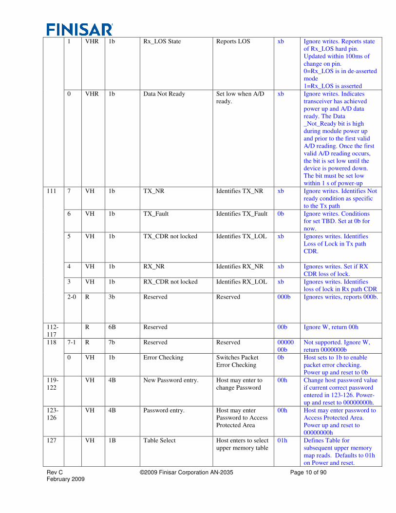
Rev C ©2009 Finisar Corporation AN-2035 Page 10 of 90 February 2009
1 VHR 1b Rx_LOS State Reports LOS xb Ignore writes. Reports state
of Rx_LOS hard pin.
Updated within 100ms of
change on pin.
0=Rx_LOS is in de-asserted
mode
1=Rx_LOS is asserted
0 VHR 1b Data Not Ready Set low when A/D
ready.
xb Ignore writes. Indicates
transceiver has achieved
power up and A/D data
ready. The Data
_Not_Ready bit is high
during module power up
and prior to the first valid
A/D reading. Once the first
valid A/D reading occurs,
the bit is set low until the
device is powered down.
The bit must be set low
within 1 s of power-up
111 7 VH 1b TX_NR Identifies TX_NR xb Ignore writes. Identifies Not
ready condition as specific
to the Tx path
6 VH 1b TX_Fault Identifies TX_Fault 0b Ignore writes. Conditions
for set TBD. Set at 0b for
now.
5 VH 1b TX_CDR not locked Identifies TX_LOL xb Ignores writes. Identifies
Loss of Lock in Tx path
CDR.
4 VH 1b RX_NR Identifies RX_NR xb Ignores writes. Set if RX
CDR loss of lock.
3 VH 1b RX_CDR not locked Identifies RX_LOL xb Ignores writes. Identifies
loss of lock in Rx path CDR
2-0 R 3b Reserved Reserved 000b Ignores writes, reports 000b.
112-
117
R 6B Reserved 00b Ignore W, return 00h
118 7-1 R 7b Reserved Reserved 00000
00b
Not supported. Ignore W,
return 0000000b
0 VH 1b Error Checking Switches Packet
Error Checking
0b Host sets to 1b to enable
packet error checking.
Power up and reset to 0b
119-
122
VH 4B New Password entry. Host may enter to
change Password
00h Change host password value
if current correct password
entered in 123-126. Power-
up and reset to 00000000h.
123-
126
VH 4B Password entry. Host may enter
Password to Access
Protected Area
00h Host may enter password to
Access Protected Area.
Power up and reset to
00000000h
127
VH 1B Table Select Host enters to select
upper memory table
01h Defines Table for
subsequent upper memory
map reads. Defaults to 01h
on Power and reset.
Rev C ©2009 Finisar Corporation AN-2035 Page 11 of 90 February 2009
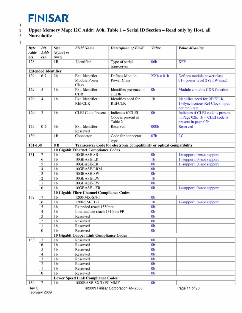
1
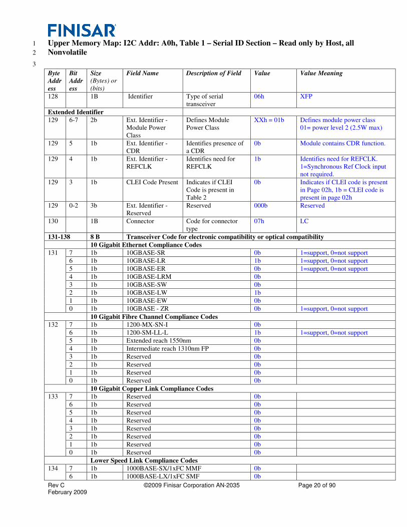
Upper Memory Map: I2C Addr: A0h, Table 1 – Serial ID Section – Read only by Host, all 2
Nonvolatile 3
4
Byte
Addr
ess
Bit
Addr
ess
Size
(Bytes) or
(bits)
Field Name Description of Field Value Value Meaning
128 1B Identifier Type of serial
transceiver
06h XFP
Extended Identifier
129 6-7 2b Ext. Identifier -
Module Power
Class
Defines Module
Power Class
XXh = 01b Defines module power class
01= power level 2 (2.5W max)
129 5 1b Ext. Identifier -
CDR
Identifies presence of
a CDR
0b Module contains CDR function.
129 4 1b Ext. Identifier -
REFCLK
Identifies need for
REFCLK
1b Identifies need for REFCLK.
1=Synchronous Ref Clock input
not required.
129 3 1b CLEI Code Present Indicates if CLEI
Code is present in
Table 2
0b Indicates if CLEI code is present
in Page 02h, 1b = CLEI code is
present in page 02h
129 0-2 3b Ext. Identifier -
Reserved
Reserved 000b Reserved
130 1B Connector Code for connector
type
07h LC
131-138 8 B Transceiver Code for electronic compatibility or optical compatibility
10 Gigabit Ethernet Compliance Codes
131 7 1b 10GBASE-SR 0b 1=support, 0=not support
6 1b 10GBASE-LR 1b 1=support, 0=not support
5 1b 10GBASE-ER 0b 1=support, 0=not support
4 1b 10GBASE-LRM 0b
3 1b 10GBASE-SW 0b
2 1b 10GBASE-LW 1b
1 1b 10GBASE-EW 0b
0 1b 10GBASE - ZR 0b 1=support, 0=not support
10 Gigabit Fibre Channel Compliance Codes
132 7 1b 1200-MX-SN-I 0b
6 1b 1200-SM-LL-L 1b 1=support, 0=not support
5 1b Extended reach 1550nm 0b
4 1b Intermediate reach 1310nm FP 0b
3 1b Reserved 0b
2 1b Reserved 0b
1 1b Reserved 0b
0 1b Reserved 0b
10 Gigabit Copper Link Compliance Codes
133 7 1b Reserved 0b
6 1b Reserved 0b
5 1b Reserved 0b
4 1b Reserved 0b
3 1b Reserved 0b
2 1b Reserved 0b
1 1b Reserved 0b
0 1b Reserved 0b
Lower Speed Link Compliance Codes
134 7 1b 1000BASE-SX/1xFC MMF 0b
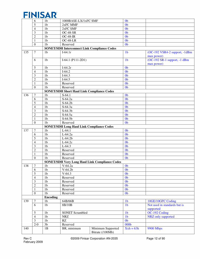
Rev C ©2009 Finisar Corporation AN-2035 Page 12 of 90 February 2009
6 1b 1000BASE-LX/1xFC SMF 0b
5 1b 2xFC MMF 0b
4 1b 2xFC SMF 0b
3 1b OC-48-SR 0b
2 1b OC-48-IR 0b
1 1b OC-48-LR 0b
0 1b Reserved 0b
SONET/SDH Interconnect Link Compliance Codes
135 7 1b I-64.1r 1b (OC-192 VSR4-2 support, -1dBm
max power)
6 1b I-64.1 (P111-2D1) 1b (OC-192 SR-1 support, -1 dBm
max power)
5 1b I-64.2r 0b
4 1b I-64.2 0b
3 1b I-64.3 0b
2 1b I-64.5 0b
1 1b Reserved 0b
0 1b Reserved 0b
SONET/SDH Short Haul Link Compliance Codes
136 7 1b S-64.1 0b
6 1b S-64.2a 0b
5 1b S-64.2b 0b
4 1b S-64.3a 0b
3 1b S-64.3b 0b
2 1b S-64.5a 0b
1 1b S-64.5b 0b
0 1b Reserved 0b
SONET/SDH Long Haul Link Compliance Codes
137 7 1b L-64.1 0b
6 1b L-64.2a 0b
5 1b L-64.2b 0b
4 1b L-64.2c 0b
3 1b L-64.3 0b
2 1b Reserved 0b
1 1b Reserved 0b
0 1b Reserved 0b
SONET/SDH Very Long Haul Link Compliance Codes
138 7 1b V-64.2a 0b
6 1b V-64.2b 0b
5 1b V-64.3 0b
4 1b Reserved 0b
3 1b Reserved 0b
2 1b Reserved 0b
1 1b Reserved 0b
0 1b Reserved 0b
Encoding
139 7 1b 64B/66B 1b 10GE/10GFC Coding
6 1b 8B/10B 1b Not used in standards but is
supported
5 1b SONET Scrambled 1b OC-192 Coding
4 1b NRZ 1b NRZ only supported
3 1b RZ 0b
2-0 3b Reserved 000b
140 1B BR, minimum Minimum Supported
Bitrate (/100Mb)
Xxh = 63h 9900 Mbps
Rev C ©2009 Finisar Corporation AN-2035 Page 13 of 90 February 2009
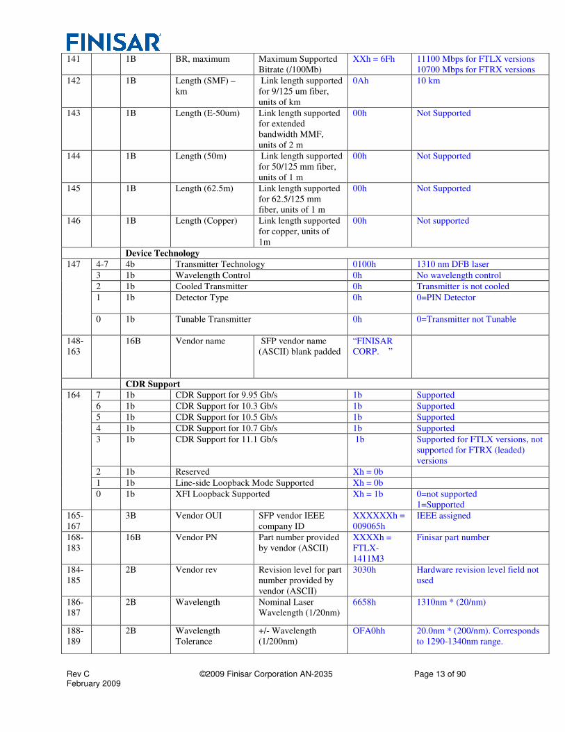
141 1B BR, maximum Maximum Supported
Bitrate (/100Mb)
XXh = 6Fh 11100 Mbps for FTLX versions
10700 Mbps for FTRX versions
142 1B Length (SMF) –
km
Link length supported
for 9/125 um fiber,
units of km
0Ah 10 km
143 1B Length (E-50um) Link length supported
for extended
bandwidth MMF,
units of 2 m
00h Not Supported
144 1B Length (50m) Link length supported
for 50/125 mm fiber,
units of 1 m
00h Not Supported
145 1B Length (62.5m) Link length supported
for 62.5/125 mm
fiber, units of 1 m
00h Not Supported
146 1B Length (Copper) Link length supported
for copper, units of
1m
00h Not supported
Device Technology
147 4-7 4b Transmitter Technology 0100h 1310 nm DFB laser
3 1b Wavelength Control 0h No wavelength control
2 1b Cooled Transmitter 0h Transmitter is not cooled
1 1b Detector Type 0h 0=PIN Detector
0 1b Tunable Transmitter 0h 0=Transmitter not Tunable
148-
163
16B Vendor name SFP vendor name
(ASCII) blank padded
“FINISAR
CORP. ”
CDR Support
164 7 1b CDR Support for 9.95 Gb/s 1b Supported
6 1b CDR Support for 10.3 Gb/s 1b Supported
5 1b CDR Support for 10.5 Gb/s 1b Supported
4 1b CDR Support for 10.7 Gb/s 1b Supported
3 1b CDR Support for 11.1 Gb/s 1b Supported for FTLX versions, not
supported for FTRX (leaded)
versions
2 1b Reserved Xh = 0b
1 1b Line-side Loopback Mode Supported Xh = 0b
0 1b XFI Loopback Supported Xh = 1b 0=not supported
1=Supported
165-
167
3B Vendor OUI SFP vendor IEEE
company ID
XXXXXXh =
009065h
IEEE assigned
168-
183
16B Vendor PN Part number provided
by vendor (ASCII)
XXXXh =
FTLX-
1411M3
Finisar part number
184-
185
2B Vendor rev Revision level for part
number provided by
vendor (ASCII)
3030h Hardware revision level field not
used
186-
187
2B Wavelength Nominal Laser
Wavelength (1/20nm)
6658h 1310nm * (20/nm)
188-
189
2B Wavelength
Tolerance
+/- Wavelength
(1/200nm)
OFA0hh 20.0nm * (200/nm). Corresponds
to 1290-1340nm range.
Rev C ©2009 Finisar Corporation AN-2035 Page 14 of 90 February 2009
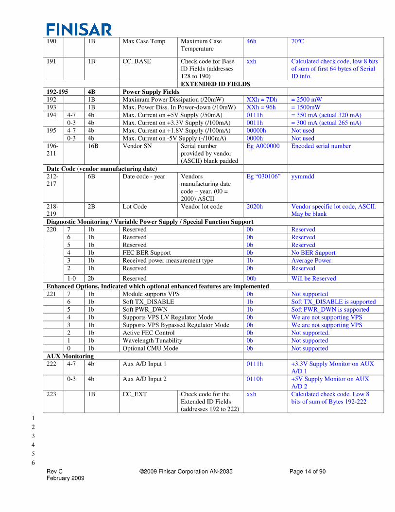
190 1B Max Case Temp Maximum Case
Temperature
46h 70ºC
191 1B CC_BASE Check code for Base
ID Fields (addresses
128 to 190)
xxh Calculated check code, low 8 bits
of sum of first 64 bytes of Serial
ID info.
EXTENDED ID FIELDS
192-195 4B Power Supply Fields
192 1B Maximum Power Dissipation (/20mW) XXh = 7Dh = 2500 mW
193 1B Max. Power Diss. In Power-down (/10mW) XXh = 96h = 1500mW
194 4-7 4b Max. Current on +5V Supply (/50mA) 0111h = 350 mA (actual 320 mA)
0-3 4b Max. Current on +3.3V Supply (/100mA) 0011h = 300 mA (actual 265 mA)
195 4-7 4b Max. Current on +1.8V Supply (/100mA) 00000h Not used
0-3 4b Max. Current on -5V Supply (-/100mA) 0000h Not used
196-
211
16B Vendor SN Serial number
provided by vendor
(ASCII) blank padded
Eg A000000 Encoded serial number
Date Code (vendor manufacturing date)
212-
217
6B Date code - year Vendors
manufacturing date
code – year. (00 =
2000) ASCII
Eg “030106” yymmdd
218-
219
2B Lot Code Vendor lot code 2020h Vendor specific lot code, ASCII.
May be blank
Diagnostic Monitoring / Variable Power Supply / Special Function Support
220 7 1b Reserved 0b Reserved
6 1b Reserved 0b Reserved
5 1b Reserved 0b Reserved
4 1b FEC BER Support 0b No BER Support
3 1b Received power measurement type 1b Average Power.
2 1b Reserved 0b Reserved
1-0 2b Reserved 00b Will be Reserved
Enhanced Options, Indicated which optional enhanced features are implemented
221 7 1b Module supports VPS 0b Not supported
6 1b Soft TX_DISABLE 1b Soft TX_DISABLE is supported
5 1b Soft PWR_DWN 1b Soft PWR_DWN is supported
4 1b Supports VPS LV Regulator Mode 0b We are not supporting VPS
3 1b Supports VPS Bypassed Regulator Mode 0b We are not supporting VPS
2 1b Active FEC Control 0b Not supported.
1 1b Wavelength Tunability 0b Not supported
0 1b Optional CMU Mode 0b Not supported
AUX Monitoring
222 4-7 4b Aux A/D Input 1 0111h +3.3V Supply Monitor on AUX
A/D 1
0-3 4b Aux A/D Input 2 0110h +5V Supply Monitor on AUX
A/D 2
223 1B CC_EXT Check code for the
Extended ID Fields
(addresses 192 to 222)
xxh Calculated check code. Low 8
bits of sum of Bytes 192-222
1
2
3
4
5
6
Rev C ©2009 Finisar Corporation AN-2035 Page 15 of 90 February 2009
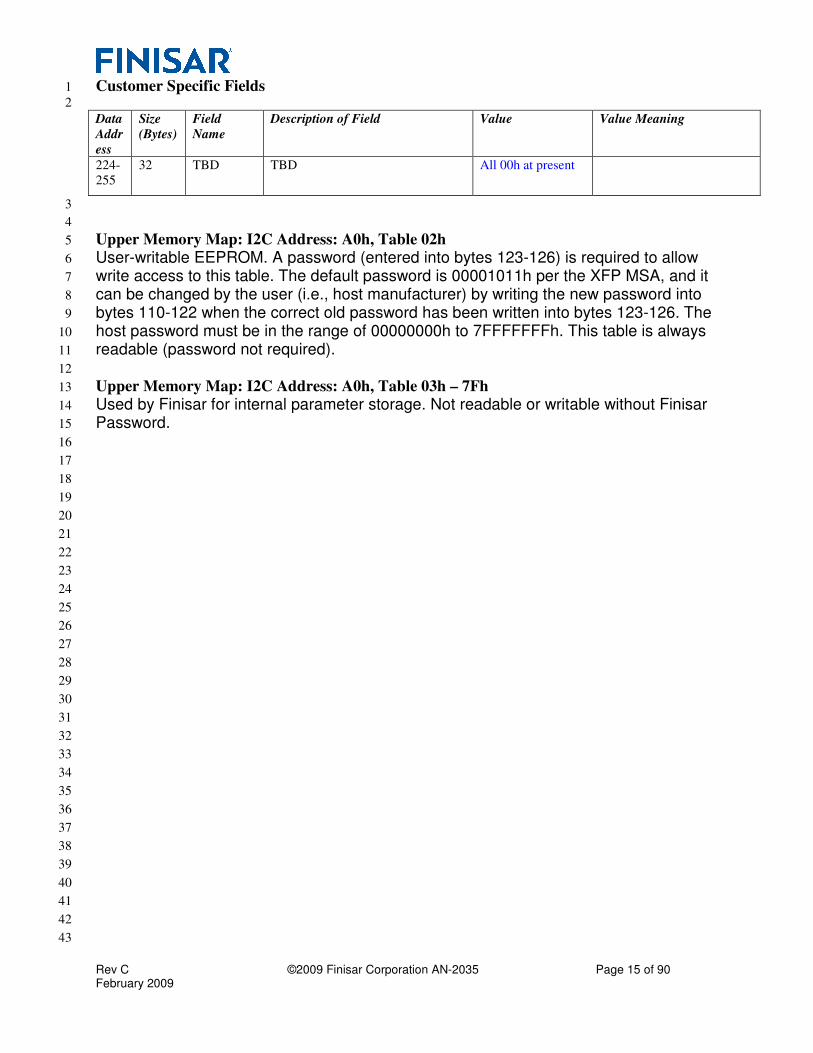
Customer Specific Fields 1
2
Data
Addr
ess
Size
(Bytes)
Field
Name
Description of Field Value Value Meaning
224-
255
32 TBD TBD All 00h at present
3
4
Upper Memory Map: I2C Address: A0h, Table 02h 5
User-writable EEPROM. A password (entered into bytes 123-126) is required to allow 6
write access to this table. The default password is 00001011h per the XFP MSA, and it 7
can be changed by the user (i.e., host manufacturer) by writing the new password into 8
bytes 110-122 when the correct old password has been written into bytes 123-126. The 9
host password must be in the range of 00000000h to 7FFFFFFFh. This table is always 10
readable (password not required). 11
12
Upper Memory Map: I2C Address: A0h, Table 03h – 7Fh 13
Used by Finisar for internal parameter storage. Not readable or writable without Finisar 14
Password. 15
16
17
18
19
20
21
22
23
24
25
26
27
28
29
30
31
32
33
34
35
36
37
38
39
40
41
42
43
Rev C ©2009 Finisar Corporation AN-2035 Page 16 of 90 February 2009
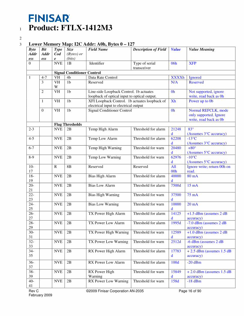
Product: FTLX-1412M3 1
2
Lower Memory Map: I2C Addr: A0h, Bytes 0 – 127 3
Byte
Addr
ess
Bit
Addr
ess
Type
Cod
e
Size
(Bytes) or
(bits)
Field Name Description of Field Value Value Meaning
0 NVE 1B Identifier Type of serial
transceiver
06h XFP
Signal Conditioner Control
1 4-7 VH 4b Data Rate Control XXXXh Ignored
3 VH
W
1b Reserved N/A Reserved
2 VH 1b Line-side Loopback Control. 1b actuates
loopback of optical input to optical output.
0h Not supported, ignore
write, read back as 0h
1 VH 1b XFI Loopback Control. 1b actuates loopback of
electrical input to electrical output
Xh Power up to 0b
0 VH 1b Signal Conditioner Control 0h Normal REFCLK, mode
only supported. Ignore
write, read back as 0b
Flag Thresholds
2-3 NVE 2B Temp High Alarm Threshold for alarm 21248
d
83°
(Assumes 3°C accuracy)
4-5 NVE 2B Temp Low Alarm Threshold for alarm 62208
d
-13°C
(Assumes 3°C accuracy)
6-7 NVE 2B Temp High Warning Threshold for warn 20480
d
+80°
(Assumes 5°C accuracy)
8-9 NVE 2B Temp Low Warning Threshold for warn 62976
d
-10°C
(Assumes 5°C accuracy)
10-
17
R 8B Reserved Reserved All
00h
Ignore write; return 00h on
read.
18-
19
NVE 2B Bias High Alarm Threshold for alarm 40000
d
80 mA
20-
21
NVE 2B Bias Low Alarm Threshold for alarm 7500d 15 mA
22-
23
NVE 2B Bias High Warning Threshold for warn 37500
d
75 mA
24-
25
NVE 2B Bias Low Warning Threshold for warn 10000
d
20 mA
26-
27
NVE 2B TX Power High Alarm Threshold for alarm 14125
d
+1.5 dBm (assumes 2 dB
accuracy)
28-
29
NVE 2B TX Power Low Alarm Threshold for alarm 1995d -7.0 dBm (assumes 2 dB
accuracy)
30-
31
NVE 2B TX Power High Warning Threshold for warn 12589
d
+1.0 dBm (assumes 2 dB
accuracy)
32-
33
NVE 2B TX Power Low Warning Threshold for warn 2512d -6 dBm (assumes 2 dB
accuracy)
34-
35
NVE 2B RX Power High Alarm Threshold for alarm 17783
d
+ 2.5 dBm (assumes 1.5 dB
accuracy)
36-
37
NVE 2B RX Power Low Alarm Threshold for alarm 100d -20 dBm
38-
39
NVE 2B RX Power High
Warning
Threshold for warn 15849
d
+ 2.0 dBm (assumes 1.5 dB
accuracy)
40-
41
NVE 2B RX Power Low Warning Threshold for warn 158d -18 dBm
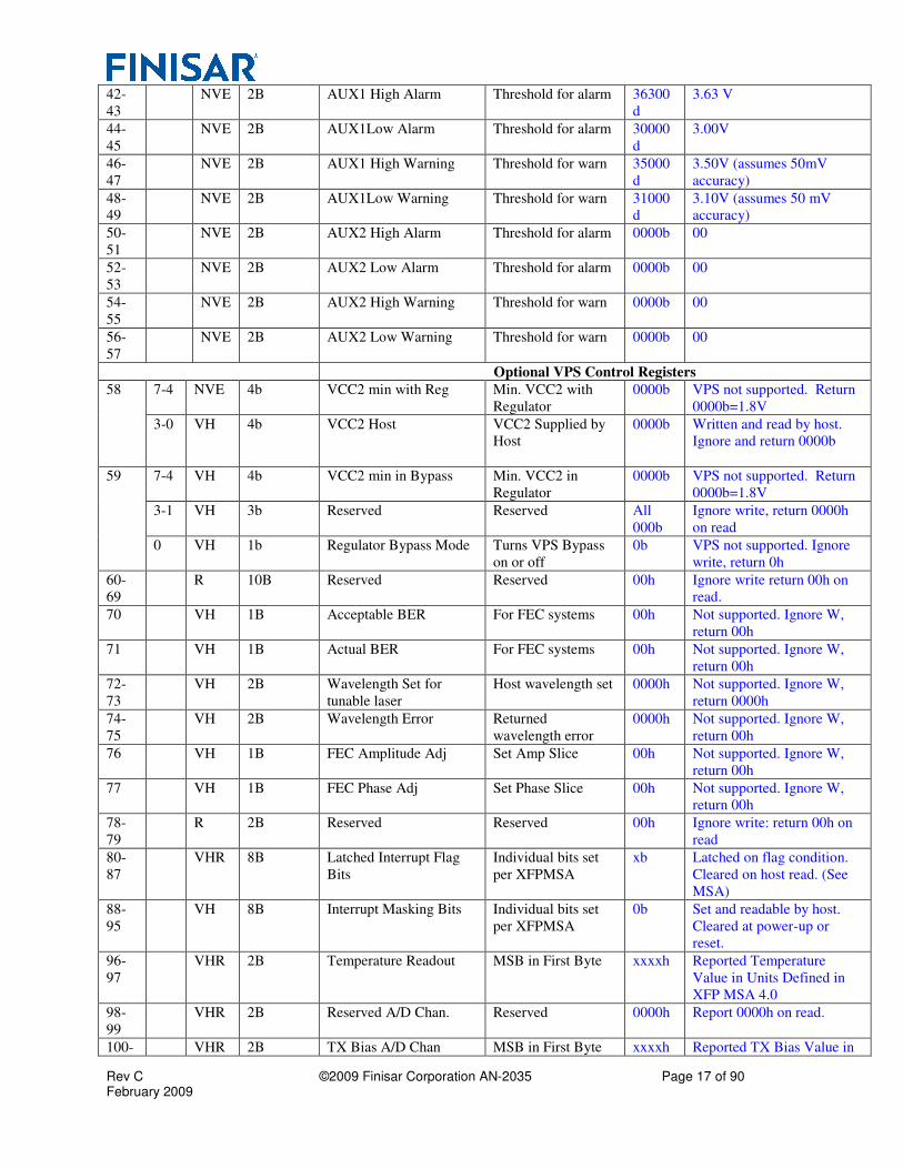
Rev C ©2009 Finisar Corporation AN-2035 Page 17 of 90 February 2009
42-
43
NVE 2B AUX1 High Alarm Threshold for alarm 36300
d
3.63 V
44-
45
NVE 2B AUX1Low Alarm Threshold for alarm 30000
d
3.00V
46-
47
NVE 2B AUX1 High Warning Threshold for warn 35000
d
3.50V (assumes 50mV
accuracy)
48-
49
NVE 2B AUX1Low Warning Threshold for warn 31000
d
3.10V (assumes 50 mV
accuracy)
50-
51
NVE 2B AUX2 High Alarm Threshold for alarm 0000b 00
52-
53
NVE 2B AUX2 Low Alarm Threshold for alarm 0000b 00
54-
55
NVE 2B AUX2 High Warning Threshold for warn 0000b 00
56-
57
NVE 2B AUX2 Low Warning Threshold for warn 0000b 00
Optional VPS Control Registers
58 7-4 NVE 4b VCC2 min with Reg Min. VCC2 with
Regulator
0000b VPS not supported. Return
0000b=1.8V
3-0 VH 4b VCC2 Host VCC2 Supplied by
Host
0000b Written and read by host.
Ignore and return 0000b
59 7-4 VH 4b VCC2 min in Bypass Min. VCC2 in
Regulator
0000b VPS not supported. Return
0000b=1.8V
3-1 VH 3b Reserved Reserved All
000b
Ignore write, return 0000h
on read
0 VH 1b Regulator Bypass Mode Turns VPS Bypass
on or off
0b VPS not supported. Ignore
write, return 0h
60-
69
R 10B Reserved Reserved 00h Ignore write return 00h on
read.
70 VH 1B Acceptable BER For FEC systems 00h Not supported. Ignore W,
return 00h
71 VH 1B Actual BER For FEC systems 00h Not supported. Ignore W,
return 00h
72-
73
VH 2B Wavelength Set for
tunable laser
Host wavelength set 0000h Not supported. Ignore W,
return 0000h
74-
75
VH 2B Wavelength Error Returned
wavelength error
0000h Not supported. Ignore W,
return 00h
76 VH 1B FEC Amplitude Adj Set Amp Slice 00h Not supported. Ignore W,
return 00h
77 VH 1B FEC Phase Adj Set Phase Slice 00h Not supported. Ignore W,
return 00h
78-
79
R 2B Reserved Reserved 00h Ignore write: return 00h on
read
80-
87
VHR 8B Latched Interrupt Flag
Bits
Individual bits set
per XFPMSA
xb Latched on flag condition.
Cleared on host read. (See
MSA)
88-
95
VH 8B Interrupt Masking Bits Individual bits set
per XFPMSA
0b Set and readable by host.
Cleared at power-up or
reset.
96-
97
VHR 2B Temperature Readout MSB in First Byte xxxxh Reported Temperature
Value in Units Defined in
XFP MSA 4.0
98-
99
VHR 2B Reserved A/D Chan. Reserved 0000h Report 0000h on read.
100- VHR 2B TX Bias A/D Chan MSB in First Byte xxxxh Reported TX Bias Value in
Rev C ©2009 Finisar Corporation AN-2035 Page 18 of 90 February 2009
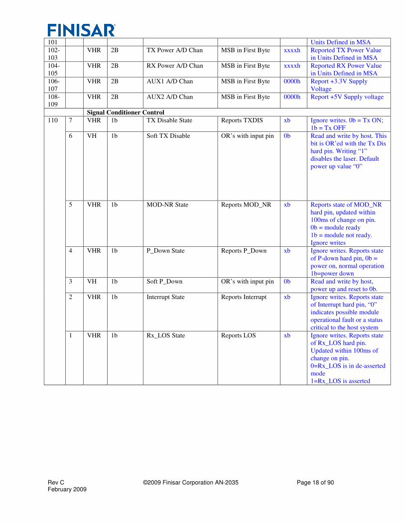
101 Units Defined in MSA
102-
103
VHR 2B TX Power A/D Chan MSB in First Byte xxxxh Reported TX Power Value
in Units Defined in MSA
104-
105
VHR 2B RX Power A/D Chan MSB in First Byte xxxxh Reported RX Power Value
in Units Defined in MSA
106-
107
VHR 2B AUX1 A/D Chan MSB in First Byte 0000h Report +3.3V Supply
Voltage
108-
109
VHR 2B AUX2 A/D Chan MSB in First Byte 0000h Report +5V Supply voltage
Signal Conditioner Control
110 7 VHR 1b TX Disable State Reports TXDIS xb Ignore writes. 0b = Tx ON;
1b = Tx OFF
6 VH 1b Soft TX Disable OR’s with input pin 0b Read and write by host. This
bit is OR’ed with the Tx Dis
hard pin. Writing “1”
disables the laser. Default
power up value “0”
5 VHR 1b MOD-NR State Reports MOD_NR xb Reports state of MOD_NR
hard pin, updated within
100ms of change on pin.
0b = module ready
1b = module not ready.
Ignore writes
4 VHR 1b P_Down State Reports P_Down xb Ignore writes. Reports state
of P-down hard pin, 0b =
power on, normal operation
1b=power down
3 VH 1b Soft P_Down OR’s with input pin 0b Read and write by host,
power up and reset to 0b.
2 VHR 1b Interrupt State Reports Interrupt xb Ignore writes. Reports state
of Interrupt hard pin, “0”
indicates possible module
operational fault or a status
critical to the host system
1 VHR 1b Rx_LOS State Reports LOS xb Ignore writes. Reports state
of Rx_LOS hard pin.
Updated within 100ms of
change on pin.
0=Rx_LOS is in de-asserted
mode
1=Rx_LOS is asserted
Rev C ©2009 Finisar Corporation AN-2035 Page 19 of 90 February 2009
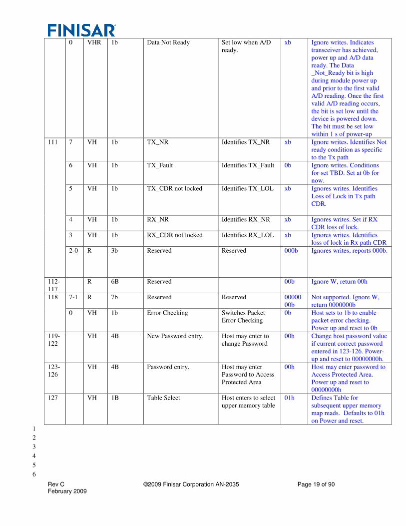
0 VHR 1b Data Not Ready Set low when A/D
ready.
xb Ignore writes. Indicates
transceiver has achieved,
power up and A/D data
ready. The Data
_Not_Ready bit is high
during module power up
and prior to the first valid
A/D reading. Once the first
valid A/D reading occurs,
the bit is set low until the
device is powered down.
The bit must be set low
within 1 s of power-up
111 7 VH 1b TX_NR Identifies TX_NR xb Ignore writes. Identifies Not
ready condition as specific
to the Tx path
6 VH 1b TX_Fault Identifies TX_Fault 0b Ignore writes. Conditions
for set TBD. Set at 0b for
now.
5 VH 1b TX_CDR not locked Identifies TX_LOL xb Ignores writes. Identifies
Loss of Lock in Tx path
CDR.
4 VH 1b RX_NR Identifies RX_NR xb Ignores writes. Set if RX
CDR loss of lock.
3 VH 1b RX_CDR not locked Identifies RX_LOL xb Ignores writes. Identifies
loss of lock in Rx path CDR
2-0 R 3b Reserved Reserved 000b Ignores writes, reports 000b.
112-
117
R 6B Reserved 00b Ignore W, return 00h
118 7-1 R 7b Reserved Reserved 00000
00b
Not supported. Ignore W,
return 0000000b
0 VH 1b Error Checking Switches Packet
Error Checking
0b Host sets to 1b to enable
packet error checking.
Power up and reset to 0b
119-
122
VH 4B New Password entry. Host may enter to
change Password
00h Change host password value
if current correct password
entered in 123-126. Power-
up and reset to 00000000h.
123-
126
VH 4B Password entry. Host may enter
Password to Access
Protected Area
00h Host may enter password to
Access Protected Area.
Power up and reset to
00000000h
127
VH 1B Table Select Host enters to select
upper memory table
01h Defines Table for
subsequent upper memory
map reads. Defaults to 01h
on Power and reset.
1
2
3
4
5
6
Rev C ©2009 Finisar Corporation AN-2035 Page 20 of 90 February 2009
Upper Memory Map: I2C Addr: A0h, Table 1 – Serial ID Section – Read only by Host, all 1
Nonvolatile 2
3
Byte
Addr
ess
Bit
Addr
ess
Size
(Bytes) or
(bits)
Field Name Description of Field Value Value Meaning
128 1B Identifier Type of serial
transceiver
06h XFP
Extended Identifier
129 6-7 2b Ext. Identifier -
Module Power
Class
Defines Module
Power Class
XXh = 01b Defines module power class
01= power level 2 (2.5W max)
129 5 1b Ext. Identifier -
CDR
Identifies presence of
a CDR
0b Module contains CDR function.
129 4 1b Ext. Identifier -
REFCLK
Identifies need for
REFCLK
1b Identifies need for REFCLK.
1=Synchronous Ref Clock input
not required.
129 3 1b CLEI Code Present Indicates if CLEI
Code is present in
Table 2
0b Indicates if CLEI code is present
in Page 02h, 1b = CLEI code is
present in page 02h
129 0-2 3b Ext. Identifier -
Reserved
Reserved 000b Reserved
130 1B Connector Code for connector
type
07h LC
131-138 8 B Transceiver Code for electronic compatibility or optical compatibility
10 Gigabit Ethernet Compliance Codes
131 7 1b 10GBASE-SR 0b 1=support, 0=not support
6 1b 10GBASE-LR 1b 1=support, 0=not support
5 1b 10GBASE-ER 0b 1=support, 0=not support
4 1b 10GBASE-LRM 0b
3 1b 10GBASE-SW 0b
2 1b 10GBASE-LW 1b
1 1b 10GBASE-EW 0b
0 1b 10GBASE - ZR 0b 1=support, 0=not support
10 Gigabit Fibre Channel Compliance Codes
132 7 1b 1200-MX-SN-I 0b
6 1b 1200-SM-LL-L 1b 1=support, 0=not support
5 1b Extended reach 1550nm 0b
4 1b Intermediate reach 1310nm FP 0b
3 1b Reserved 0b
2 1b Reserved 0b
1 1b Reserved 0b
0 1b Reserved 0b
10 Gigabit Copper Link Compliance Codes
133 7 1b Reserved 0b
6 1b Reserved 0b
5 1b Reserved 0b
4 1b Reserved 0b
3 1b Reserved 0b
2 1b Reserved 0b
1 1b Reserved 0b
0 1b Reserved 0b
Lower Speed Link Compliance Codes
134 7 1b 1000BASE-SX/1xFC MMF 0b
6 1b 1000BASE-LX/1xFC SMF 0b
Rev C ©2009 Finisar Corporation AN-2035 Page 21 of 90 February 2009
5 1b 2xFC MMF 0b
4 1b 2xFC SMF 0b
3 1b OC-48-SR 0b
2 1b OC-48-IR 0b
1 1b OC-48-LR 0b
0 1b Reserved 0b
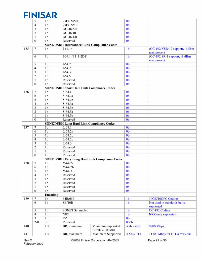
SONET/SDH Interconnect Link Compliance Codes
135 7 1b I-64.1r 1b (OC-192 VSR4-2 support, -1dBm
max power)
6 1b I-64.1 (P111-2D1) 1b (OC-192 SR-1 support, -1 dBm
max power)
5 1b I-64.2r 0b
4 1b I-64.2 0b
3 1b I-64.3 0b
2 1b I-64.5 0b
1 1b Reserved 0b
0 1b Reserved 0b
SONET/SDH Short Haul Link Compliance Codes
136 7 1b S-64.1 0b
6 1b S-64.2a 0b
5 1b S-64.2b 0b
4 1b S-64.3a 0b
3 1b S-64.3b 0b
2 1b S-64.5a 0b
1 1b S-64.5b 0b
0 1b Reserved 0b
SONET/SDH Long Haul Link Compliance Codes
137 7 1b L-64.1 0b
6 1b L-64.2a 0b
5 1b L-64.2b 0b
4 1b L-64.2c 0b
3 1b L-64.3 0b
2 1b Reserved 0b
1 1b Reserved 0b
0 1b Reserved 0b
SONET/SDH Very Long Haul Link Compliance Codes
138 7 1b V-64.2a 0b
6 1b V-64.2b 0b
5 1b V-64.3 0b
4 1b Reserved 0b
3 1b Reserved 0b
2 1b Reserved 0b
1 1b Reserved 0b
0 1b Reserved 0b
Encoding
139 7 1b 64B/66B 1b 10GE/10GFC Coding
6 1b 8B/10B 1b Not used in standards but is
supported
5 1b SONET Scrambled 1b OC-192 Coding
4 1b NRZ 1b NRZ only supported
3 1b RZ 0b
2-0 3b Reserved 000b
140 1B BR, minimum Minimum Supported
Bitrate (/100Mb)
Xxh = 63h 9900 Mbps
141 1B BR, maximum Maximum Supported XXh = 71h 11300 Mbps for FTLX versions
Rev C ©2009 Finisar Corporation AN-2035 Page 22 of 90 February 2009
Bitrate (/100Mb)
142 1B Length (SMF) –
km
Link length supported
for 9/125 um fiber,
units of km
0Ah 10 km
143 1B Length (E-50um) Link length supported
for extended
bandwidth MMF,
units of 2 m
00h Not Supported
144 1B Length (50m) Link length supported
for 50/125 mm fiber,
units of 1 m
00h Not Supported
145 1B Length (62.5m) Link length supported
for 62.5/125 mm
fiber, units of 1 m
00h Not Supported
146 1B Length (Copper) Link length supported
for copper, units of
1m
00h Not supported
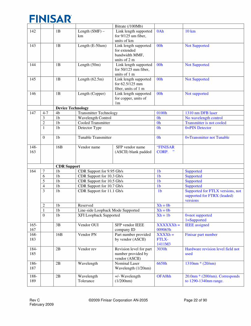
Device Technology
147 4-7 4b Transmitter Technology 0100h 1310 nm DFB laser
3 1b Wavelength Control 0h No wavelength control
2 1b Cooled Transmitter 0h Transmitter is not cooled
1 1b Detector Type 0h 0=PIN Detector
0 1b Tunable Transmitter 0h 0=Transmitter not Tunable
148-
163
16B Vendor name SFP vendor name
(ASCII) blank padded
“FINISAR
CORP. ”
CDR Support
164 7 1b CDR Support for 9.95 Gb/s 1b Supported
6 1b CDR Support for 10.3 Gb/s 1b Supported
5 1b CDR Support for 10.5 Gb/s 1b Supported
4 1b CDR Support for 10.7 Gb/s 1b Supported
3 1b CDR Support for 11.1 Gb/s 1b Supported for FTLX versions, not
supported for FTRX (leaded)
versions
2 1b Reserved Xh = 0b
1 1b Line-side Loopback Mode Supported Xh = 0b
0 1b XFI Loopback Supported Xh = 1b 0=not supported
1=Supported
165-
167
3B Vendor OUI SFP vendor IEEE
company ID
XXXXXXh =
009065h
IEEE assigned
168-
183
16B Vendor PN Part number provided
by vendor (ASCII)
XXXXh =
FTLX-
1411M3
Finisar part number
184-
185
2B Vendor rev Revision level for part
number provided by
vendor (ASCII)
3030h Hardware revision level field not
used
186-
187
2B Wavelength Nominal Laser
Wavelength (1/20nm)
6658h 1310nm * (20/nm)
188-
189
2B Wavelength
Tolerance
+/- Wavelength
(1/200nm)
OFA0hh 20.0nm * (200/nm). Corresponds
to 1290-1340nm range.
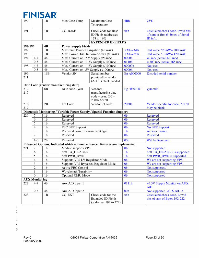
Rev C ©2009 Finisar Corporation AN-2035 Page 23 of 90 February 2009
190 1B Max Case Temp Maximum Case
Temperature
4Bh 75ºC
191 1B CC_BASE Check code for Base
ID Fields (addresses
128 to 190)
xxh Calculated check code, low 8 bits
of sum of first 64 bytes of Serial
ID info.
EXTENDED ID FIELDS
192-195 4B Power Supply Fields
192 1B Maximum Power Dissipation (/20mW) XXh = 64h 8bit value *20mW= 2000mW
193 1B Max. Power Diss. In Power-down (/10mW) XXh = 96h 8bit value *10mW= 1200mW
194 4-7 4b Max. Current on +5V Supply (/50mA) 0000h =0 mA (actual 320 mA)
0-3 4b Max. Current on +3.3V Supply (/100mA) 0110h = 300 mA (actual 265 mA)
195 4-7 4b Max. Current on +1.8V Supply (/100mA) 00000h Not used
0-3 4b Max. Current on -5V Supply (-/100mA) 0000h Not used
196-
211
16B Vendor SN Serial number
provided by vendor
(ASCII) blank padded
Eg A000000 Encoded serial number
Date Code (vendor manufacturing date)
212-
217
6B Date code - year Vendors
manufacturing date
code – year. (00 =
2000) ASCII
Eg “030106” yymmdd
218-
219
2B Lot Code Vendor lot code 2020h Vendor specific lot code, ASCII.
May be blank
Diagnostic Monitoring / Variable Power Supply / Special Function Support
220 7 1b Reserved 0b Reserved
6 1b Reserved 0b Reserved
5 1b Reserved 0b Reserved
4 1b FEC BER Support 0b No BER Support
3 1b Received power measurement type 1b Average Power.
2 1b Reserved 0b Reserved
1-0 2b Reserved 00b Will be Reserved
Enhanced Options, Indicated which optional enhanced features are implemented
221 7 1b Module supports VPS 0b Not supported
6 1b Soft TX_DISABLE 1b Soft TX_DISABLE is supported
5 1b Soft PWR_DWN 1b Soft PWR_DWN is supported
4 1b Supports VPS LV Regulator Mode 0b We are not supporting VPS
3 1b Supports VPS Bypassed Regulator Mode 0b We are not supporting VPS
2 1b Active FEC Control 0b Not supported.
1 1b Wavelength Tunability 0b Not supported
0 1b Optional CMU Mode 0b Not supported
AUX Monitoring
222 4-7 4b Aux A/D Input 1 0111h +3.3V Supply Monitor on AUX
A/D 1
0-3 4b Aux A/D Input 2 00h Not supported AUX A/D 2
223 1B CC_EXT Check code for the
Extended ID Fields
(addresses 192 to 222)
xxh Calculated check code. Low 8
bits of sum of Bytes 192-222
1
2
3
4
5
6

Rev C ©2009 Finisar Corporation AN-2035 Page 24 of 90 February 2009
Customer Specific Fields 1
2
Data
Addr
ess
Size
(Bytes)
Field
Name
Description of Field Value Value Meaning
224-
255
32 TBD TBD All 00h at present
3
4
Upper Memory Map: I2C Address: A0h, Table 02h 5
User-writable EEPROM. A password (entered into bytes 123-126) is required to allow 6
write access to this table. The default password is 00001011h per the XFP MSA, and it 7
can be changed by the user (i.e., host manufacturer) by writing the new password into 8
bytes 110-122 when the correct old password has been written into bytes 123-126. The 9
host password must be in the range of 00000000h to 7FFFFFFFh. This table is always 10
readable (password not required). 11
12
Upper Memory Map: I2C Address: A0h, Table 03h – 7Fh 13
Used by Finisar for internal parameter storage. Not readable or writable without Finisar 14
Password. 15
16
17
18
19
20
21
22
23
24
25
26
27
28
29
30
31
32
33
34
35
36
37
38
39
40
41
42
43
Rev C ©2009 Finisar Corporation AN-2035 Page 25 of 90 February 2009
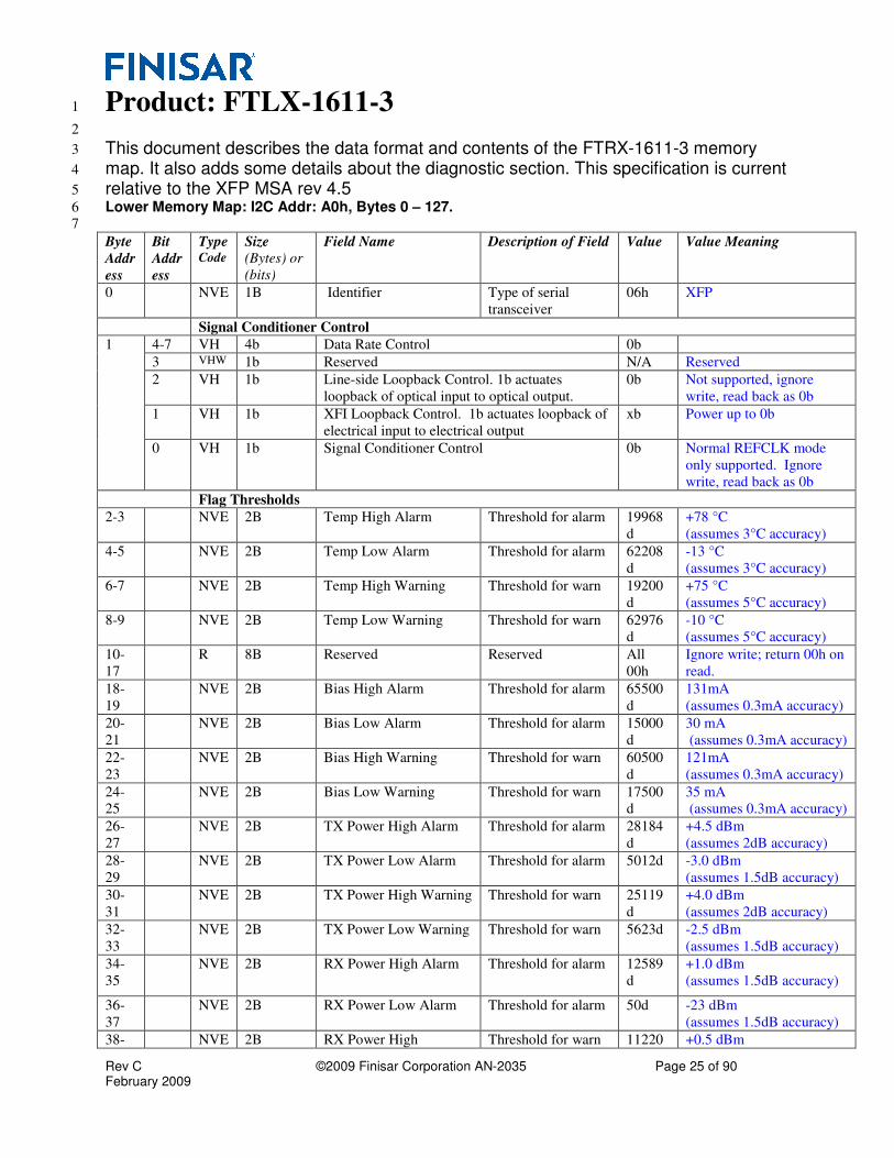
Product: FTLX-1611-3 1
2
This document describes the data format and contents of the FTRX-1611-3 memory 3
map. It also adds some details about the diagnostic section. This specification is current 4
relative to the XFP MSA rev 4.5 5
Lower Memory Map: I2C Addr: A0h, Bytes 0 – 127. 6
7
Byte
Addr
ess
Bit
Addr
ess
Type Code
Size
(Bytes) or
(bits)
Field Name Description of Field Value Value Meaning
0 NVE 1B Identifier Type of serial
transceiver
06h XFP
Signal Conditioner Control
1 4-7 VH 4b Data Rate Control 0b
3 VHW 1b Reserved N/A Reserved
2 VH 1b Line-side Loopback Control. 1b actuates
loopback of optical input to optical output.
0b Not supported, ignore
write, read back as 0b
1 VH 1b XFI Loopback Control. 1b actuates loopback of
electrical input to electrical output
xb Power up to 0b
0 VH 1b Signal Conditioner Control 0b Normal REFCLK mode
only supported. Ignore
write, read back as 0b
Flag Thresholds
2-3 NVE 2B Temp High Alarm Threshold for alarm 19968
d
+78 °C
(assumes 3°C accuracy)
4-5 NVE 2B Temp Low Alarm Threshold for alarm 62208
d
-13 °C
(assumes 3°C accuracy)
6-7 NVE 2B Temp High Warning Threshold for warn 19200
d
+75 °C
(assumes 5°C accuracy)
8-9 NVE 2B Temp Low Warning Threshold for warn 62976
d
-10 °C
(assumes 5°C accuracy)
10-
17
R 8B Reserved Reserved All
00h
Ignore write; return 00h on
read.
18-
19
NVE 2B Bias High Alarm Threshold for alarm 65500
d
131mA
(assumes 0.3mA accuracy)
20-
21
NVE 2B Bias Low Alarm Threshold for alarm 15000
d
30 mA
(assumes 0.3mA accuracy)
22-
23
NVE 2B Bias High Warning Threshold for warn 60500
d
121mA
(assumes 0.3mA accuracy)
24-
25
NVE 2B Bias Low Warning Threshold for warn 17500
d
35 mA
(assumes 0.3mA accuracy)
26-
27
NVE 2B TX Power High Alarm Threshold for alarm 28184
d
+4.5 dBm
(assumes 2dB accuracy)
28-
29
NVE 2B TX Power Low Alarm Threshold for alarm 5012d -3.0 dBm
(assumes 1.5dB accuracy)
30-
31
NVE 2B TX Power High Warning Threshold for warn 25119
d
+4.0 dBm
(assumes 2dB accuracy)
32-
33
NVE 2B TX Power Low Warning Threshold for warn 5623d -2.5 dBm
(assumes 1.5dB accuracy)
34-
35
NVE 2B RX Power High Alarm Threshold for alarm 12589
d
+1.0 dBm
(assumes 1.5dB accuracy)
36-
37
NVE 2B RX Power Low Alarm Threshold for alarm 50d -23 dBm
(assumes 1.5dB accuracy)
38- NVE 2B RX Power High Threshold for warn 11220 +0.5 dBm
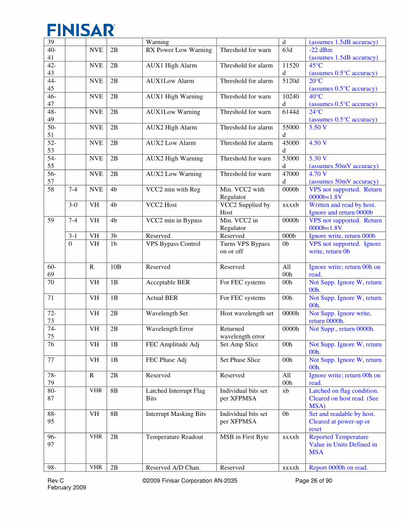
Rev C ©2009 Finisar Corporation AN-2035 Page 26 of 90 February 2009
39 Warning d (assumes 1.5dB accuracy)
40-
41
NVE 2B RX Power Low Warning Threshold for warn 63d -22 dBm
(assumes 1.5dB accuracy)
42-
43
NVE 2B AUX1 High Alarm Threshold for alarm 11520
d
45°C
(assumes 0.5°C accuracy)
44-
45
NVE 2B AUX1Low Alarm Threshold for alarm 5120d 20°C
(assumes 0.5°C accuracy)
46-
47
NVE 2B AUX1 High Warning Threshold for warn 10240
d
40°C
(assumes 0.5°C accuracy)
48-
49
NVE 2B AUX1Low Warning Threshold for warn 6144d 24°C
(assumes 0.5°C accuracy)
50-
51
NVE 2B AUX2 High Alarm Threshold for alarm 55000
d
5.50 V
52-
53
NVE 2B AUX2 Low Alarm Threshold for alarm 45000
d
4.50 V
54-
55
NVE 2B AUX2 High Warning Threshold for warn 53000
d
5.30 V
(assumes 50mV accuracy)
56-
57
NVE 2B AUX2 Low Warning Threshold for warn 47000
d
4.70 V
(assumes 50mV accuracy)
58 7-4 NVE 4b VCC2 min with Reg Min. VCC2 with
Regulator
0000b VPS not supported. Return
0000b=1.8V
3-0 VH 4b VCC2 Host VCC2 Supplied by
Host
xxxxb Written and read by host.
Ignore and return 0000b
59 7-4 VH 4b VCC2 min in Bypass Min. VCC2 in
Regulator
0000b VPS not supported. Return
0000b=1.8V
3-1 VH 3b Reserved Reserved 000b Ignore write, return 000b
0 VH 1b VPS Bypass Control Turns VPS Bypass
on or off
0b VPS not supported. Ignore
write, return 0b
60-
69
R 10B Reserved Reserved All
00h
Ignore write; return 00h on
read.
70 VH 1B Acceptable BER For FEC systems 00h Not Supp. Ignore W, return
00h.
71 VH 1B Actual BER For FEC systems 00h Not Supp. Ignore W, return
00h.
72-
73
VH 2B Wavelength Set Host wavelength set 0000h Not Supp. Ignore write,
return 0000h.
74-
75
VH 2B Wavelength Error Returned
wavelength error
0000h Not Supp., return 0000h.
76 VH 1B FEC Amplitude Adj Set Amp Slice 00h Not Supp. Ignore W, return
00h.
77 VH 1B FEC Phase Adj Set Phase Slice 00h Not Supp. Ignore W, return
00h.
78-
79
R 2B Reserved Reserved All
00h
Ignore write; return 00h on
read.
80-
87
VHR 8B Latched Interrupt Flag
Bits
Individual bits set
per XFPMSA
xb Latched on flag condition.
Cleared on host read. (See
MSA)
88-
95
VH 8B Interrupt Masking Bits Individual bits set
per XFPMSA
0b Set and readable by host.
Cleared at power-up or
reset
96-
97
VHR 2B Temperature Readout MSB in First Byte xxxxh Reported Temperature
Value in Units Defined in
MSA
98- VHR 2B Reserved A/D Chan. Reserved xxxxh Report 0000h on read.
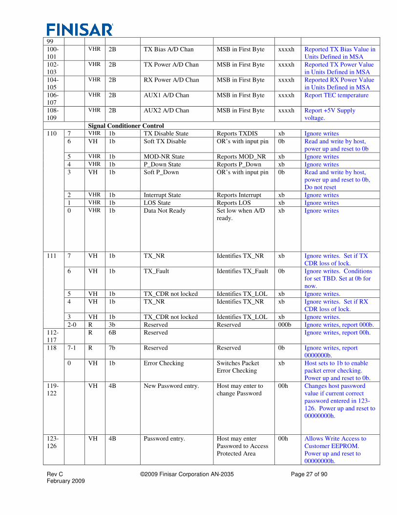
Rev C ©2009 Finisar Corporation AN-2035 Page 27 of 90 February 2009
99
100-
101
VHR 2B TX Bias A/D Chan MSB in First Byte xxxxh Reported TX Bias Value in
Units Defined in MSA
102-
103
VHR 2B TX Power A/D Chan MSB in First Byte xxxxh Reported TX Power Value
in Units Defined in MSA
104-
105
VHR 2B RX Power A/D Chan MSB in First Byte xxxxh Reported RX Power Value
in Units Defined in MSA
106-
107
VHR 2B AUX1 A/D Chan MSB in First Byte xxxxh Report TEC temperature
108-
109
VHR 2B AUX2 A/D Chan MSB in First Byte xxxxh Report +5V Supply
voltage.
Signal Conditioner Control
110 7 VHR 1b TX Disable State Reports TXDIS xb Ignore writes
6 VH 1b Soft TX Disable OR’s with input pin 0b Read and write by host,
power up and reset to 0b
5 VHR 1b MOD-NR State Reports MOD_NR xb Ignore writes
4 VHR 1b P_Down State Reports P_Down xb Ignore writes
3 VH 1b Soft P_Down OR’s with input pin 0b Read and write by host,
power up and reset to 0b,
Do not reset
2 VHR 1b Interrupt State Reports Interrupt xb Ignore writes
1 VHR 1b LOS State Reports LOS xb Ignore writes
0 VHR 1b Data Not Ready
Set low when A/D
ready.
xb Ignore writes
111 7 VH 1b TX_NR Identifies TX_NR xb Ignore writes. Set if TX
CDR loss of lock.
6 VH 1b TX_Fault Identifies TX_Fault 0b Ignore writes. Conditions
for set TBD. Set at 0b for
now.
5 VH 1b TX_CDR not locked Identifies TX_LOL xb Ignore writes.
4 VH 1b TX_NR Identifies TX_NR xb Ignore writes. Set if RX
CDR loss of lock.
3 VH 1b TX_CDR not locked Identifies TX_LOL xb Ignore writes.
2-0 R 3b Reserved Reserved 000b Ignore writes, report 000b.
112-
117
R 6B Reserved Ignore writes, report 00h.
118 7-1 R 7b Reserved Reserved 0b Ignore writes, report
0000000b.
0 VH 1b Error Checking Switches Packet
Error Checking
xb Host sets to 1b to enable
packet error checking.
Power up and reset to 0b.
119-
122
VH 4B New Password entry. Host may enter to
change Password
00h Changes host password
value if current correct
password entered in 123-
126. Power up and reset to
00000000h.
123-
126
VH 4B Password entry. Host may enter
Password to Access
Protected Area
00h Allows Write Access to
Customer EEPROM.
Power up and reset to
00000000h.
Rev C ©2009 Finisar Corporation AN-2035 Page 28 of 90 February 2009
127 VH 1B Table Select Host enters to select
upper memory table
01h Defines Table for
subsequent upper memory
map reads. Defaults to 01h
on Power and reset.
1
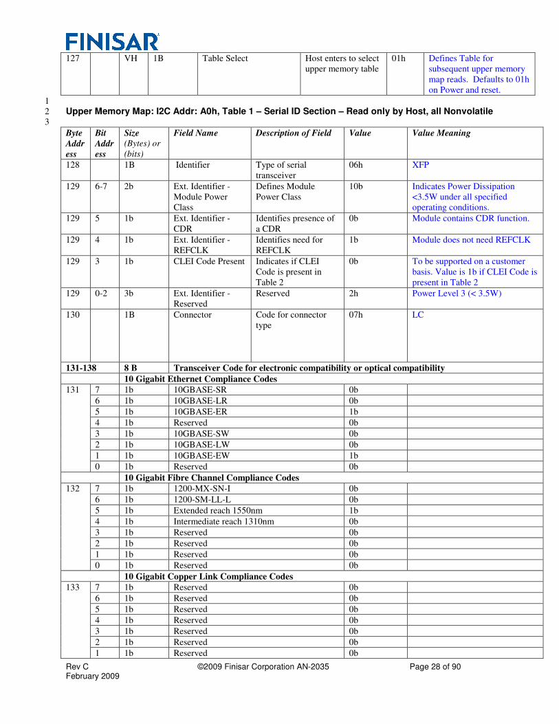
Upper Memory Map: I2C Addr: A0h, Table 1 – Serial ID Section – Read only by Host, all Nonvolatile 2
3
Byte
Addr
ess
Bit
Addr
ess
Size
(Bytes) or
(bits)
Field Name Description of Field Value Value Meaning
128 1B Identifier Type of serial
transceiver
06h XFP
129 6-7 2b Ext. Identifier -
Module Power
Class
Defines Module
Power Class
10b Indicates Power Dissipation
<3.5W under all specified
operating conditions.
129 5 1b Ext. Identifier -
CDR
Identifies presence of
a CDR
0b Module contains CDR function.
129 4 1b Ext. Identifier -
REFCLK
Identifies need for
REFCLK
1b Module does not need REFCLK
129 3 1b CLEI Code Present Indicates if CLEI
Code is present in
Table 2
0b To be supported on a customer
basis. Value is 1b if CLEI Code is
present in Table 2
129 0-2 3b Ext. Identifier -
Reserved
Reserved 2h Power Level 3 (< 3.5W)
130 1B Connector Code for connector
type
07h LC
131-138 8 B Transceiver Code for electronic compatibility or optical compatibility
10 Gigabit Ethernet Compliance Codes
131 7 1b 10GBASE-SR 0b
6 1b 10GBASE-LR 0b
5 1b 10GBASE-ER 1b
4 1b Reserved 0b
3 1b 10GBASE-SW 0b
2 1b 10GBASE-LW 0b
1 1b 10GBASE-EW 1b
0 1b Reserved 0b
10 Gigabit Fibre Channel Compliance Codes
132 7 1b 1200-MX-SN-I 0b
6 1b 1200-SM-LL-L 0b
5 1b Extended reach 1550nm 1b
4 1b Intermediate reach 1310nm 0b
3 1b Reserved 0b
2 1b Reserved 0b
1 1b Reserved 0b
0 1b Reserved 0b
10 Gigabit Copper Link Compliance Codes
133 7 1b Reserved 0b
6 1b Reserved 0b
5 1b Reserved 0b
4 1b Reserved 0b
3 1b Reserved 0b
2 1b Reserved 0b
1 1b Reserved 0b
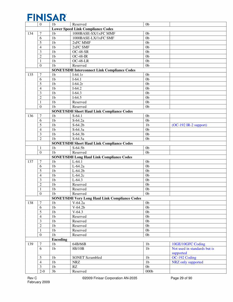
Rev C ©2009 Finisar Corporation AN-2035 Page 29 of 90 February 2009
0 1b Reserved 0b
Lower Speed Link Compliance Codes
134 7 1b 1000BASE-SX/1xFC MMF 0b
6 1b 1000BASE-LX/1xFC SMF 0b
5 1b 2xFC MMF 0b
4 1b 2xFC SMF 0b
3 1b OC-48-SR 0b
2 1b OC-48-IR 0b
1 1b OC-48-LR 0b
0 1b Reserved 0b
SONET/SDH Interconnect Link Compliance Codes
135 7 1b I-64.1r 0b
6 1b I-64.1 0b
5 1b I-64.2r 0b
4 1b I-64.2 0b
3 1b I-64.3 0b
2 1b I-64.5 0b
1 1b Reserved 0b
0 1b Reserved 0b
SONET/SDH Short Haul Link Compliance Codes
136 7 1b S-64.1 0b
6 1b S-64.2a 0b
5 1b S-64.2b 1b (OC-192 IR-2 support)
4 1b S-64.3a 0b
3 1b S-64.3b 0b
2 1b S-64.5a 0b
SONET/SDH Short Haul Link Compliance Codes
1 1b S-64.5b 0b
0 1b Reserved 0b
SONET/SDH Long Haul Link Compliance Codes
137 7 1b L-64.1 0b
6 1b L-64.2a 0b
5 1b L-64.2b 0b
4 1b L-64.2c 0b
3 1b L-64.3 0b
2 1b Reserved 0b
1 1b Reserved 0b
0 1b Reserved 0b
SONET/SDH Very Long Haul Link Compliance Codes
138 7 1b V-64.2a 0b
6 1b V-64.2b 0b
5 1b V-64.3 0b
4 1b Reserved 0b
3 1b Reserved 0b
2 1b Reserved 0b
1 1b Reserved 0b
0 1b Reserved 0b
Encoding
139 7 1b 64B/66B 1b 10GE/10GFC Coding
6 1b 8B/10B 1b Not used in standards but is
supported
5 1b SONET Scrambled 1b OC-192 Coding
4 1b NRZ 1b NRZ only supported
3 1b RZ 0b
2-0 3b Reserved 000b
Rev C ©2009 Finisar Corporation AN-2035 Page 30 of 90 February 2009
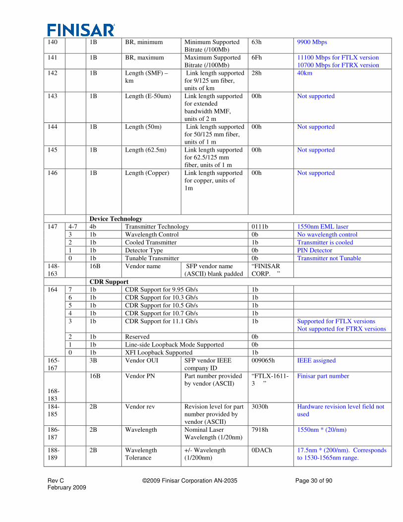
140 1B BR, minimum Minimum Supported
Bitrate (/100Mb)
63h 9900 Mbps
141 1B BR, maximum Maximum Supported
Bitrate (/100Mb)
6Fh 11100 Mbps for FTLX version
10700 Mbps for FTRX version
142 1B Length (SMF) –
km
Link length supported
for 9/125 um fiber,
units of km
28h 40km
143 1B Length (E-50um) Link length supported
for extended
bandwidth MMF,
units of 2 m
00h Not supported
144 1B Length (50m) Link length supported
for 50/125 mm fiber,
units of 1 m
00h Not supported
145 1B Length (62.5m) Link length supported
for 62.5/125 mm
fiber, units of 1 m
00h Not supported
146 1B Length (Copper) Link length supported
for copper, units of
1m
00h Not supported
Device Technology
147 4-7 4b Transmitter Technology 0111b 1550nm EML laser
3 1b Wavelength Control 0b No wavelength control
2 1b Cooled Transmitter 1b Transmitter is cooled
1 1b Detector Type 0b PIN Detector
0 1b Tunable Transmitter 0b Transmitter not Tunable
148-
163
16B Vendor name SFP vendor name
(ASCII) blank padded
“FINISAR
CORP. ”
CDR Support
164 7 1b CDR Support for 9.95 Gb/s 1b
6 1b CDR Support for 10.3 Gb/s 1b
5 1b CDR Support for 10.5 Gb/s 1b
4 1b CDR Support for 10.7 Gb/s 1b
3 1b CDR Support for 11.1 Gb/s 1b Supported for FTLX versions
Not supported for FTRX versions
2 1b Reserved 0b
1 1b Line-side Loopback Mode Supported 0b
0 1b XFI Loopback Supported 1b
165-
167
3B Vendor OUI SFP vendor IEEE
company ID
009065h IEEE assigned
168-
183
16B Vendor PN Part number provided
by vendor (ASCII)
“FTLX-1611-
3 ”
Finisar part number
184-
185
2B Vendor rev Revision level for part
number provided by
vendor (ASCII)
3030h Hardware revision level field not
used
186-
187
2B Wavelength Nominal Laser
Wavelength (1/20nm)
7918h 1550nm * (20/nm)
188-
189
2B Wavelength
Tolerance
+/- Wavelength
(1/200nm)
0DACh 17.5nm * (200/nm). Corresponds
to 1530-1565nm range.
Rev C ©2009 Finisar Corporation AN-2035 Page 31 of 90 February 2009
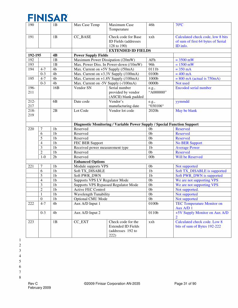
190 1B Max Case Temp Maximum Case
Temperature
46h 70ºC
191 1B CC_BASE Check code for Base
ID Fields (addresses
128 to 190)
xxh Calculated check code, low 8 bits
of sum of first 64 bytes of Serial
ID info.
EXTENDED ID FIELDS
192-195 4B Power Supply Fields
192 1B Maximum Power Dissipation (/20mW) AFh = 3500 mW
193 1B Max. Power Diss. In Power-down (/10mW) 96h = 1500 mW
194 4-7 4b Max. Current on +5V Supply (/50mA) 0111b = 350 mA
0-3 4b Max. Current on +3.3V Supply (/100mA) 0100b = 400 mA
195 4-7 4b Max. Current on +1.8V Supply (/100mA) 1000b = 800 mA (actual is 750mA)
0-3 4b Max. Current on -5V Supply (-/100mA) 0000b Not used
196-
211
16B Vendor SN Serial number
provided by vendor
(ASCII) blank padded
e.g.,
“A000000”
Encoded serial number
212-
217
6B Date code Vendor’s
manufacturing date
e.g.,
“030106“
yymmdd
218-
219
2B Lot Code Vendor lot code 2020h May be blank
Diagnostic Monitoring / Variable Power Supply / Special Function Support
220 7 1b Reserved 0b Reserved
6 1b Reserved 0b Reserved
5 1b Reserved 0b Reserved
4 1b FEC BER Support 0b No BER Support
3 1b Received power measurement type 1b Average Power
2 1b Reserved 0b Reserved
1-0 2b Reserved 00b Will be Reserved
Enhanced Options
221 7 1b Module supports VPS 0b Not supported
6 1b Soft TX_DISABLE 1b Soft TX_DISABLE is supported
5 1b Soft PWR_DWN 1b Soft PWR_DWN is supported
4 1b Supports VPS LV Regulator Mode 0b We are not supporting VPS
3 1b Supports VPS Bypassed Regulator Mode 0b We are not supporting VPS
2 1b Active FEC Control 0b Not supported.
1 1b Wavelength Tunability 0b Not supported
0 1b Optional CMU Mode 0b Not supported
222 4-7 4b Aux A/D Input 1 0100b TEC Temperature Monitor on
Aux A/D 1
0-3 4b Aux A/D Input 2 0110b +5V Supply Monitor on Aux A/D
2
223 1B CC_EXT Check code for the
Extended ID Fields
(addresses 192 to
222)
xxh Calculated check code. Low 8
bits of sum of Bytes 192-222
1
2
3
4
5
6
7
8
Rev C ©2009 Finisar Corporation AN-2035 Page 32 of 90 February 2009
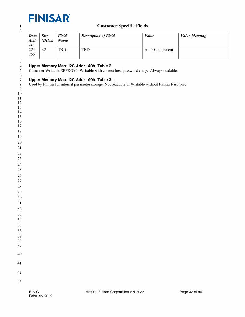
Customer Specific Fields 1
2
Data
Addr
ess
Size
(Bytes)
Field
Name
Description of Field Value Value Meaning
224-
255
32 TBD TBD All 00h at present
3
Upper Memory Map: I2C Addr: A0h, Table 2 4
Customer Writable EEPROM. Writable with correct host password entry. Always readable. 5
6
Upper Memory Map: I2C Addr: A0h, Table 3– 7
Used by Finisar for internal parameter storage. Not readable or Writable without Finisar Password. 8
9
10
11
12
13
14
15
16
17
18
19
20
21
22
23
24
25
26
27
28
29
30
31
32
33
34
35
36
37
38
39
40
41
42
43
Rev C ©2009 Finisar Corporation AN-2035 Page 33 of 90 February 2009
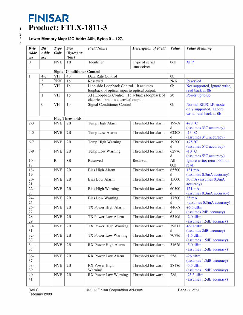
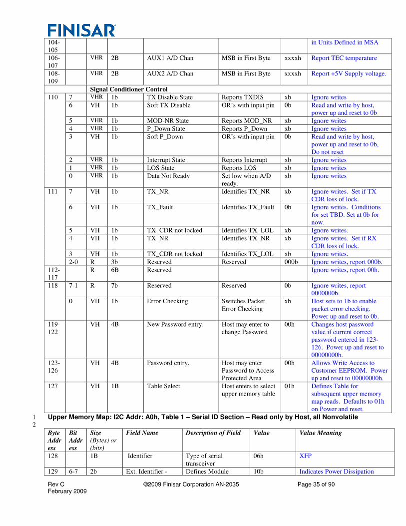
Product: FTLX-1811-3 1
2
Lower Memory Map: I2C Addr: A0h, Bytes 0 – 127. 3
4
Byte
Addr
ess
Bit
Addr
ess
Type Code
Size
(Bytes) or
(bits)
Field Name Description of Field Value Value Meaning
0 NVE 1B Identifier Type of serial
transceiver
06h XFP
Signal Conditioner Control
1 4-7 VH 4b Data Rate Control 0b
3 VHW 1b Reserved N/A Reserved
2 VH 1b Line-side Loopback Control. 1b actuates
loopback of optical input to optical output.
0b Not supported, ignore write,
read back as 0b
1 VH 1b XFI Loopback Control. 1b actuates loopback of
electrical input to electrical output
xb Power up to 0b
0 VH 1b Signal Conditioner Control 0b Normal REFCLK mode
only supported. Ignore
write, read back as 0b
Flag Thresholds
2-3 NVE 2B Temp High Alarm Threshold for alarm 19968
d
+78 °C
(assumes 3°C accuracy)
4-5 NVE 2B Temp Low Alarm Threshold for alarm 62208
d
-13 °C
(assumes 3°C accuracy)
6-7 NVE 2B Temp High Warning Threshold for warn 19200
d
+75 °C
(assumes 5°C accuracy)
8-9 NVE 2B Temp Low Warning Threshold for warn 62976
d
-10 °C
(assumes 5°C accuracy)
10-
17
R 8B Reserved Reserved All
00h
Ignore write; return 00h on
read.
18-
19
NVE 2B Bias High Alarm Threshold for alarm 65500
d
131 mA
(assumes 0.3mA accuracy)
20-
21
NVE 2B Bias Low Alarm Threshold for alarm 15000
d
30 mA (assumes 0.3mA
accuracy)
22-
23
NVE 2B Bias High Warning Threshold for warn 60500
d
121 mA
(assumes 0.3mA accuracy)
24-
25
NVE 2B Bias Low Warning Threshold for warn 17500
d
35 mA
(assumes 0.3mA accuracy)
26-
27
NVE 2B TX Power High Alarm Threshold for alarm 44668
d
+6.5 dBm
(assumes 2dB accuracy)
28-
29
NVE 2B TX Power Low Alarm Threshold for alarm 6310d -2.0 dBm
(assumes 1.5dB accuracy)
30-
31
NVE 2B TX Power High Warning Threshold for warn 39811
d
+6.0 dBm
(assumes 2dB accuracy)
32-
33
NVE 2B TX Power Low Warning Threshold for warn 7079d -1.5 dBm
(assumes 1.5dB accuracy)
34-
35
NVE 2B RX Power High Alarm Threshold for alarm 3162d -5.0 dBm
(assumes 1.5dB accuracy)
36-
37
NVE 2B RX Power Low Alarm Threshold for alarm 25d -26 dBm
(assumes 1.5dB accuracy)
38-
39
NVE 2B RX Power High
Warning
Threshold for warn 2818d -5.5 dBm
(assumes 1.5dB accuracy)
40-
41
NVE 2B RX Power Low Warning Threshold for warn 28d -25.5 dBm
(assumes 1.5dB accuracy)
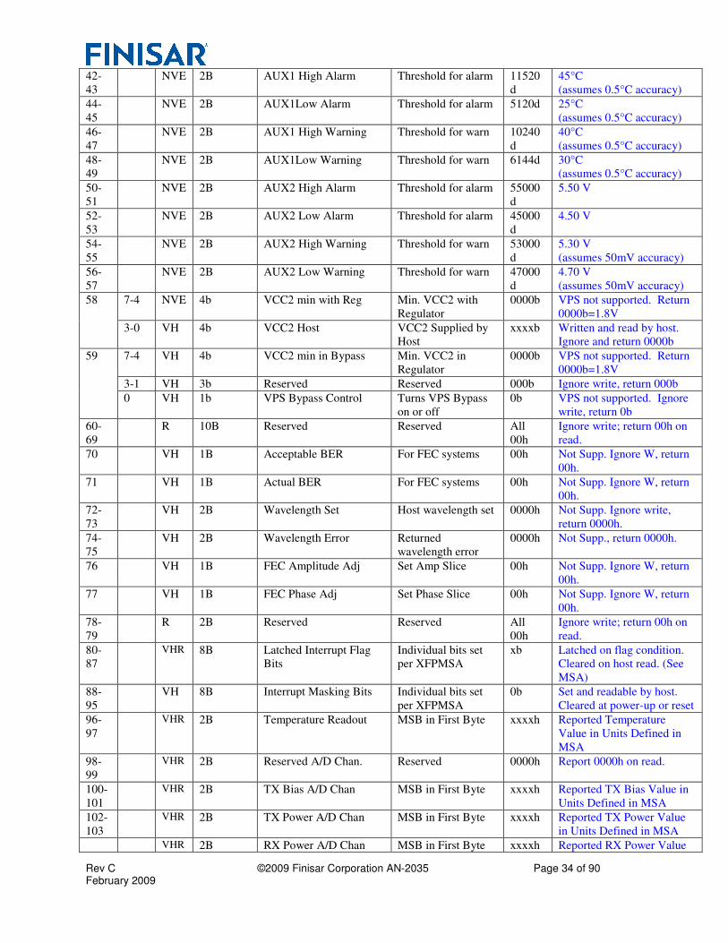
Rev C ©2009 Finisar Corporation AN-2035 Page 34 of 90 February 2009
42-
43
NVE 2B AUX1 High Alarm Threshold for alarm 11520
d
45°C
(assumes 0.5°C accuracy)
44-
45
NVE 2B AUX1Low Alarm Threshold for alarm 5120d 25°C
(assumes 0.5°C accuracy)
46-
47
NVE 2B AUX1 High Warning Threshold for warn 10240
d
40°C
(assumes 0.5°C accuracy)
48-
49
NVE 2B AUX1Low Warning Threshold for warn 6144d 30°C
(assumes 0.5°C accuracy)
50-
51
NVE 2B AUX2 High Alarm Threshold for alarm 55000
d
5.50 V
52-
53
NVE 2B AUX2 Low Alarm Threshold for alarm 45000
d
4.50 V
54-
55
NVE 2B AUX2 High Warning Threshold for warn 53000
d
5.30 V
(assumes 50mV accuracy)
56-
57
NVE 2B AUX2 Low Warning Threshold for warn 47000
d
4.70 V
(assumes 50mV accuracy)
58 7-4 NVE 4b VCC2 min with Reg Min. VCC2 with
Regulator
0000b VPS not supported. Return
0000b=1.8V
3-0 VH 4b VCC2 Host VCC2 Supplied by
Host
xxxxb Written and read by host.
Ignore and return 0000b
59 7-4 VH 4b VCC2 min in Bypass Min. VCC2 in
Regulator
0000b VPS not supported. Return
0000b=1.8V
3-1 VH 3b Reserved Reserved 000b Ignore write, return 000b
0 VH 1b VPS Bypass Control Turns VPS Bypass
on or off
0b VPS not supported. Ignore
write, return 0b
60-
69
R 10B Reserved Reserved All
00h
Ignore write; return 00h on
read.
70 VH 1B Acceptable BER For FEC systems 00h Not Supp. Ignore W, return
00h.
71 VH 1B Actual BER For FEC systems 00h Not Supp. Ignore W, return
00h.
72-
73
VH 2B Wavelength Set Host wavelength set 0000h Not Supp. Ignore write,
return 0000h.
74-
75
VH 2B Wavelength Error Returned
wavelength error
0000h Not Supp., return 0000h.
76 VH 1B FEC Amplitude Adj Set Amp Slice 00h Not Supp. Ignore W, return
00h.
77 VH 1B FEC Phase Adj Set Phase Slice 00h Not Supp. Ignore W, return
00h.
78-
79
R 2B Reserved Reserved All
00h
Ignore write; return 00h on
read.
80-
87
VHR 8B Latched Interrupt Flag
Bits
Individual bits set
per XFPMSA
xb Latched on flag condition.
Cleared on host read. (See
MSA)
88-
95
VH 8B Interrupt Masking Bits Individual bits set
per XFPMSA
0b Set and readable by host.
Cleared at power-up or reset
96-
97
VHR 2B Temperature Readout MSB in First Byte xxxxh Reported Temperature
Value in Units Defined in
MSA
98-
99
VHR 2B Reserved A/D Chan. Reserved 0000h Report 0000h on read.
100-
101
VHR 2B TX Bias A/D Chan MSB in First Byte xxxxh Reported TX Bias Value in
Units Defined in MSA
102-
103
VHR 2B TX Power A/D Chan MSB in First Byte xxxxh Reported TX Power Value
in Units Defined in MSA
VHR 2B RX Power A/D Chan MSB in First Byte xxxxh Reported RX Power Value
Rev C ©2009 Finisar Corporation AN-2035 Page 35 of 90 February 2009
104-
105
in Units Defined in MSA
106-
107
VHR 2B AUX1 A/D Chan MSB in First Byte xxxxh Report TEC temperature
108-
109
VHR 2B AUX2 A/D Chan MSB in First Byte xxxxh Report +5V Supply voltage.
Signal Conditioner Control
110 7 VHR 1b TX Disable State Reports TXDIS xb Ignore writes
6 VH 1b Soft TX Disable OR’s with input pin 0b Read and write by host,
power up and reset to 0b
5 VHR 1b MOD-NR State Reports MOD_NR xb Ignore writes
4 VHR 1b P_Down State Reports P_Down xb Ignore writes
3 VH 1b Soft P_Down OR’s with input pin 0b Read and write by host,
power up and reset to 0b,
Do not reset
2 VHR 1b Interrupt State Reports Interrupt xb Ignore writes
1 VHR 1b LOS State Reports LOS xb Ignore writes
0 VHR 1b Data Not Ready Set low when A/D
ready.
xb Ignore writes
111 7 VH 1b TX_NR Identifies TX_NR xb Ignore writes. Set if TX
CDR loss of lock.
6 VH 1b TX_Fault Identifies TX_Fault 0b Ignore writes. Conditions
for set TBD. Set at 0b for
now.
5 VH 1b TX_CDR not locked Identifies TX_LOL xb Ignore writes.
4 VH 1b TX_NR Identifies TX_NR xb Ignore writes. Set if RX
CDR loss of lock.
3 VH 1b TX_CDR not locked Identifies TX_LOL xb Ignore writes.
2-0 R 3b Reserved Reserved 000b Ignore writes, report 000b.
112-
117
R 6B Reserved Ignore writes, report 00h.
118 7-1 R 7b Reserved Reserved 0b Ignore writes, report
0000000b.
0 VH 1b Error Checking Switches Packet
Error Checking
xb Host sets to 1b to enable
packet error checking.
Power up and reset to 0b.
119-
122
VH 4B New Password entry. Host may enter to
change Password
00h Changes host password
value if current correct
password entered in 123-
126. Power up and reset to
00000000h.
123-
126
VH 4B Password entry. Host may enter
Password to Access
Protected Area
00h Allows Write Access to
Customer EEPROM. Power
up and reset to 00000000h.
127 VH 1B Table Select Host enters to select
upper memory table
01h Defines Table for
subsequent upper memory
map reads. Defaults to 01h
on Power and reset.
Upper Memory Map: I2C Addr: A0h, Table 1 – Serial ID Section – Read only by Host, all Nonvolatile 1
2
Byte
Addr
ess
Bit
Addr
ess
Size (Bytes) or
(bits)
Field Name Description of Field Value Value Meaning
128 1B Identifier Type of serial
transceiver
06h XFP
129 6-7 2b Ext. Identifier - Defines Module 10b Indicates Power Dissipation
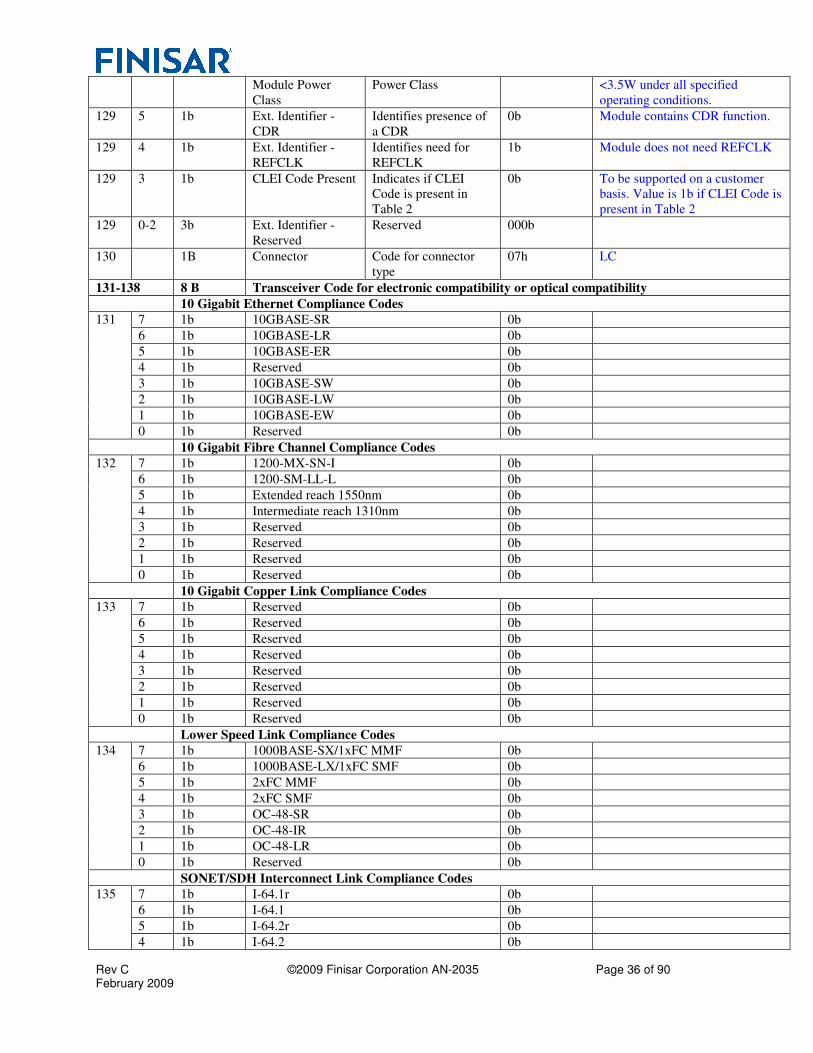
Rev C ©2009 Finisar Corporation AN-2035 Page 36 of 90 February 2009
Module Power
Class
Power Class <3.5W under all specified
operating conditions.
129 5 1b Ext. Identifier -
CDR
Identifies presence of
a CDR
0b Module contains CDR function.
129 4 1b Ext. Identifier -
REFCLK
Identifies need for
REFCLK
1b Module does not need REFCLK
129 3 1b CLEI Code Present Indicates if CLEI
Code is present in
Table 2
0b To be supported on a customer
basis. Value is 1b if CLEI Code is
present in Table 2
129 0-2 3b Ext. Identifier -
Reserved
Reserved 000b
130 1B Connector Code for connector
type
07h LC
131-138 8 B Transceiver Code for electronic compatibility or optical compatibility
10 Gigabit Ethernet Compliance Codes
131 7 1b 10GBASE-SR 0b
6 1b 10GBASE-LR 0b
5 1b 10GBASE-ER 0b
4 1b Reserved 0b
3 1b 10GBASE-SW 0b
2 1b 10GBASE-LW 0b
1 1b 10GBASE-EW 0b
0 1b Reserved 0b
10 Gigabit Fibre Channel Compliance Codes
132 7 1b 1200-MX-SN-I 0b
6 1b 1200-SM-LL-L 0b
5 1b Extended reach 1550nm 0b
4 1b Intermediate reach 1310nm 0b
3 1b Reserved 0b
2 1b Reserved 0b
1 1b Reserved 0b
0 1b Reserved 0b
10 Gigabit Copper Link Compliance Codes
133 7 1b Reserved 0b
6 1b Reserved 0b
5 1b Reserved 0b
4 1b Reserved 0b
3 1b Reserved 0b
2 1b Reserved 0b
1 1b Reserved 0b
0 1b Reserved 0b
Lower Speed Link Compliance Codes
134 7 1b 1000BASE-SX/1xFC MMF 0b
6 1b 1000BASE-LX/1xFC SMF 0b
5 1b 2xFC MMF 0b
4 1b 2xFC SMF 0b
3 1b OC-48-SR 0b
2 1b OC-48-IR 0b
1 1b OC-48-LR 0b
0 1b Reserved 0b
SONET/SDH Interconnect Link Compliance Codes
135 7 1b I-64.1r 0b
6 1b I-64.1 0b
5 1b I-64.2r 0b
4 1b I-64.2 0b
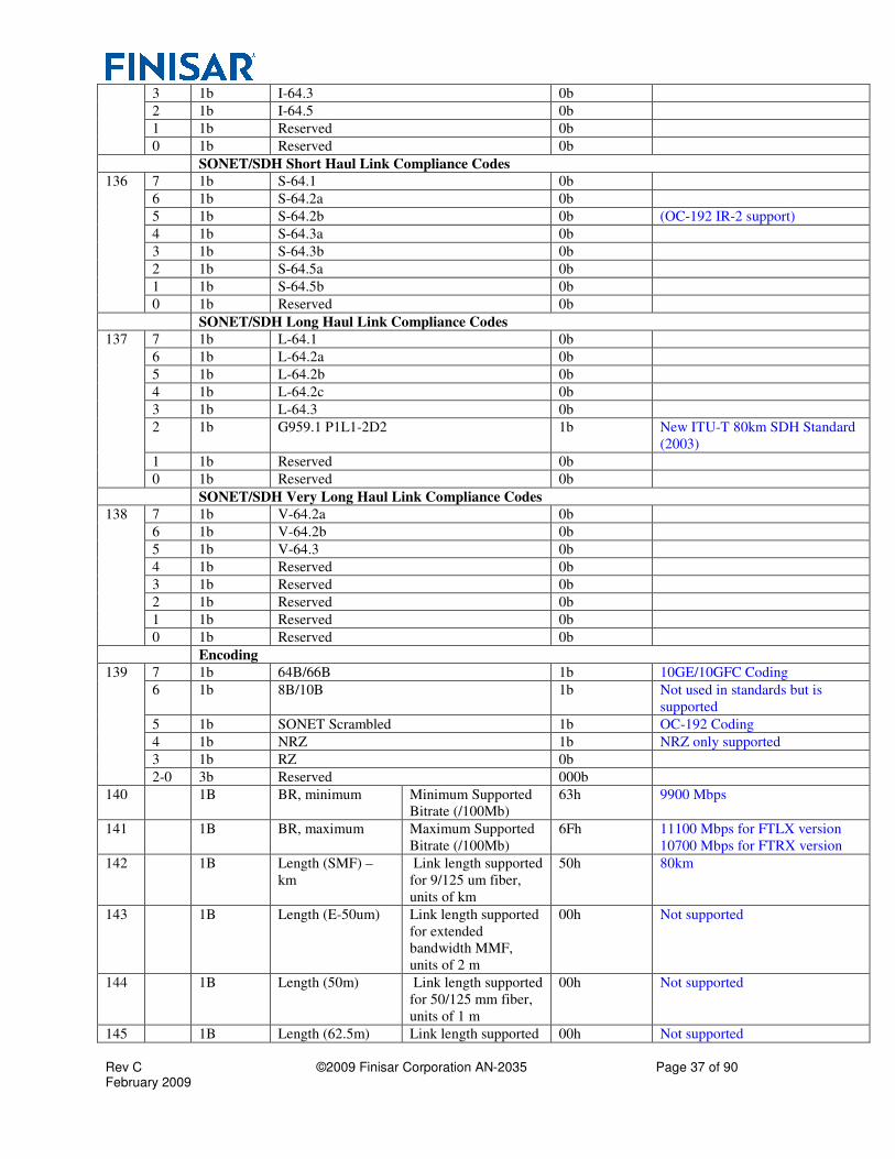
Rev C ©2009 Finisar Corporation AN-2035 Page 37 of 90 February 2009
3 1b I-64.3 0b
2 1b I-64.5 0b
1 1b Reserved 0b
0 1b Reserved 0b
SONET/SDH Short Haul Link Compliance Codes
136 7 1b S-64.1 0b
6 1b S-64.2a 0b
5 1b S-64.2b 0b (OC-192 IR-2 support)
4 1b S-64.3a 0b
3 1b S-64.3b 0b
2 1b S-64.5a 0b
1 1b S-64.5b 0b
0 1b Reserved 0b
SONET/SDH Long Haul Link Compliance Codes
137 7 1b L-64.1 0b
6 1b L-64.2a 0b
5 1b L-64.2b 0b
4 1b L-64.2c 0b
3 1b L-64.3 0b
2 1b G959.1 P1L1-2D2 1b New ITU-T 80km SDH Standard
(2003)
1 1b Reserved 0b
0 1b Reserved 0b
SONET/SDH Very Long Haul Link Compliance Codes
138 7 1b V-64.2a 0b
6 1b V-64.2b 0b
5 1b V-64.3 0b
4 1b Reserved 0b
3 1b Reserved 0b
2 1b Reserved 0b
1 1b Reserved 0b
0 1b Reserved 0b
Encoding
139 7 1b 64B/66B 1b 10GE/10GFC Coding
6 1b 8B/10B 1b Not used in standards but is
supported
5 1b SONET Scrambled 1b OC-192 Coding
4 1b NRZ 1b NRZ only supported
3 1b RZ 0b
2-0 3b Reserved 000b
140 1B BR, minimum Minimum Supported
Bitrate (/100Mb)
63h 9900 Mbps
141 1B BR, maximum Maximum Supported
Bitrate (/100Mb)
6Fh 11100 Mbps for FTLX version
10700 Mbps for FTRX version
142 1B Length (SMF) –
km
Link length supported
for 9/125 um fiber,
units of km
50h 80km
143 1B Length (E-50um) Link length supported
for extended
bandwidth MMF,
units of 2 m
00h Not supported
144 1B Length (50m) Link length supported
for 50/125 mm fiber,
units of 1 m
00h Not supported
145 1B Length (62.5m) Link length supported 00h Not supported

Rev C ©2009 Finisar Corporation AN-2035 Page 38 of 90 February 2009
for 62.5/125 mm
fiber, units of 1 m
146 1B Length (Copper) Link length supported
for copper, units of
1m
00h Not supported
Device Technology
147 4-7 4b Transmitter Technology 0111b 1550nm EML laser
3 1b Wavelength Control 0b No wavelength control
2 1b Cooled Transmitter 1b Transmitter is cooled
1 1b Detector Type 1b APD Detector
0 1b Tunable Transmitter 0b Transmitter not Tunable
148-
163
16B Vendor name SFP vendor name
(ASCII) blank padded
“FINISAR
CORP. ”
CDR Support
164 7 1b CDR Support for 9.95 Gb/s 1b
6 1b CDR Support for 10.3 Gb/s 1b
5 1b CDR Support for 10.5 Gb/s 1b
4 1b CDR Support for 10.7 Gb/s 1b
3 1b CDR Support for 11.1 Gb/s 1b Supported for FTLX versions
Not supported for FTRX versions
2 1b Reserved 0b
1 1b Line-side Loopback Mode Supported 0b
0 1b XFI Loopback Supported 1b
165-
167
3B Vendor OUI SFP vendor IEEE
company ID
009065h IEEE assigned
168-
183
16B Vendor PN Part number provided
by vendor (ASCII)
“FTLX-1811-
3 ”
Finisar part number
184-
185
2B Vendor rev Revision level for part
number provided by
vendor (ASCII)
3030h Hardware revision level field not
used
186-
187
2B Wavelength Nominal Laser
Wavelength (1/20nm)
7918h 1550nm * (20/nm)
188-
189
2B Wavelength
Tolerance
+/- Wavelength
(1/200nm)
0DACh 17.5nm * (200/nm). Corresponds
to 1530-1565nm range.
190 1B Max Case Temp Maximum Case
Temperature
46h 70ºC
191 1B CC_BASE Check code for Base
ID Fields (addresses
128 to 190)
xxh Calculated check code, low 8 bits
of sum of first 64 bytes of Serial
ID info.
EXTENDED ID FIELDS
192-195 4B Power Supply Fields
192 1B Maximum Power Dissipation (/20mW) AFh = 3500 mW
193 1B Max. Power Diss. In Power-down (/10mW) 96h = 1500 mW
194 4-7 4b Max. Current on +5V Supply (/50mA) 0111b = 350 mA
0-3 4b Max. Current on +3.3V Supply (/100mA) 0100b = 400 mA
195 4-7 4b Max. Current on +1.8V Supply (/100mA) 1000b = 800 mA (actual is 750mA)
0-3 4b Max. Current on -5V Supply (-/100mA) 0000b Not used
196-
211
16B Vendor SN Serial number
provided by vendor
(ASCII) blank padded
e.g.,
“A000000”
Encoded serial number
212-
217
6B Date code Vendor’s
manufacturing date
e.g.,
“030106“
yymmdd
218-
219
2B Lot Code Vendor lot code 2020h May be blank
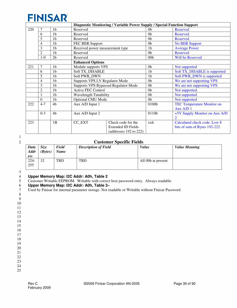
Rev C ©2009 Finisar Corporation AN-2035 Page 39 of 90 February 2009
Diagnostic Monitoring / Variable Power Supply / Special Function Support
220 7 1b Reserved 0b Reserved
6 1b Reserved 0b Reserved
5 1b Reserved 0b Reserved
4 1b FEC BER Support 0b No BER Support
3 1b Received power measurement type 1b Average Power
2 1b Reserved 0b Reserved
1-0 2b Reserved 00b Will be Reserved
Enhanced Options
221 7 1b Module supports VPS 0b Not supported
6 1b Soft TX_DISABLE 1b Soft TX_DISABLE is supported
5 1b Soft PWR_DWN 1b Soft PWR_DWN is supported
4 1b Supports VPS LV Regulator Mode 0b We are not supporting VPS
3 1b Supports VPS Bypassed Regulator Mode 0b We are not supporting VPS
2 1b Active FEC Control 0b Not supported.
1 1b Wavelength Tunability 0b Not supported
0 1b Optional CMU Mode 0b Not supported
222 4-7 4b Aux A/D Input 1 0100b TEC Temperature Monitor on
Aux A/D 1
0-3 4b Aux A/D Input 2 0110b +5V Supply Monitor on Aux A/D
2
223 1B CC_EXT Check code for the
Extended ID Fields
(addresses 192 to 222)
xxh Calculated check code. Low 8
bits of sum of Bytes 192-222
1
Customer Specific Fields 2
Data
Addr
ess
Size
(Bytes)
Field
Name
Description of Field Value Value Meaning
224-
255
32 TBD TBD All 00h at present
3
Upper Memory Map: I2C Addr: A0h, Table 2 4 Customer Writable EEPROM. Writable with correct host password entry. Always readable. 5
Upper Memory Map: I2C Addr: A0h, Table 3– 6
Used by Finisar for internal parameter storage. Not readable or Writable without Finisar Password. 7
8
9
10
11
12
13
14
15
16
17
18
19
20
21
22
23
24
25
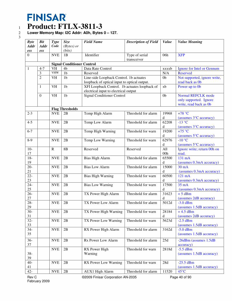
Rev C ©2009 Finisar Corporation AN-2035 Page 40 of 90 February 2009
Product: FTLX-3811-3 1
Lower Memory Map: I2C Addr: A0h, Bytes 0 – 127. 2
3
Byte
Addr
ess
Bit
Addr
ess
Type Code
Size
(Bytes) or
(bits)
Field Name Description of Field Value Value Meaning
0 NVE 1B Identifier Type of serial
transceiver
06h XFP
Signal Conditioner Control
1 4-7 VH 4b Data Rate Control xxxxb Ignore for Intel or Gennum
3 VHW 1b Reserved N/A Reserved
2 VH 1b Line-side Loopback Control. 1b actuates
loopback of optical input to optical output.
0b Not supported, ignore write,
read back as 0b
1 VH 1b XFI Loopback Control. 1b actuates loopback of
electrical input to electrical output
xb Power up to 0b
0 VH 1b Signal Conditioner Control 0b Normal REFCLK mode
only supported. Ignore
write, read back as 0b
Flag Thresholds
2-3 NVE 2B Temp High Alarm Threshold for alarm 19968
d
+78 °C
(assumes 3°C accuracy)
4-5 NVE 2B Temp Low Alarm Threshold for alarm 62208
d
-13 °C
(assumes 3°C accuracy)
6-7 NVE 2B Temp High Warning Threshold for warn 19200
d
+75 °C
(assumes 5°C accuracy)
8-9 NVE 2B Temp Low Warning Threshold for warn 62976
d
-10 °C
(assumes 5°C accuracy)
10-
17
R 8B Reserved Reserved All
00h
Ignore write; return 00h on
read.
18-
19
NVE 2B Bias High Alarm Threshold for alarm 65500
d
131 mA
(assumes 0.3mA accuracy)
20-
21
NVE 2B Bias Low Alarm Threshold for alarm 15000
d
30 mA
(assumes 0.3mA accuracy)
22-
23
NVE 2B Bias High Warning Threshold for warn 60500
d
121 mA
(assumes 0.3mA accuracy)
24-
25
NVE 2B Bias Low Warning Threshold for warn 17500
d
35 mA
(assumes 0.3mA accuracy)
26-
27
NVE 2B TX Power High Alarm Threshold for alarm 31623
d
+ 5 dBm
(assumes 2dB accuracy)
28-
29
NVE 2B TX Power Low Alarm Threshold for alarm 5012d -3.0 dBm
(assumes 1.5dB accuracy)
30-
31
NVE 2B TX Power High Warning Threshold for warn 28184
d
+ 4.5 dBm
(assumes 2dB accuracy)
32-
33
NVE 2B TX Power Low Warning Threshold for warn 5623d -2.5 dBm
(assumes 1.5dB accuracy)
34-
35
NVE 2B RX Power High Alarm Threshold for alarm 3162d -5.0 dBm
(assumes 1.5dB accuracy)
36-
37
NVE 2B Rx Power Low Alarm Threshold for alarm 25d -26dBm (assumes 1.5dB
accuracy)
38-
39
NVE 2B RX Power High
Warning
Threshold for warn 2818d -5.5 dBm
(assumes 1.5dB accuracy)
40-
41
NVE 2B RX Power Low Warning Threshold for warn 28d -25.5 dBm
(assumes 1.5dB accuracy)
42- NVE 2B AUX1 High Alarm Threshold for alarm 11520 45°C

Rev C ©2009 Finisar Corporation AN-2035 Page 41 of 90 February 2009
43 d (assumes 0.5°C accuracy)
44-
45
NVE 2B AUX1Low Alarm Threshold for alarm 5120d 25°C
(assumes 0.5°C accuracy)
46-
47
NVE 2B AUX1 High Warning Threshold for warn 10240
d
40°C
(assumes 0.5°C accuracy)
48-
49
NVE 2B AUX1Low Warning Threshold for warn 6144d 30°C
(assumes 0.5°C accuracy)
50-
51
NVE 2B AUX2 High Alarm Threshold for alarm 55000
d
5.50 V
52-
53
NVE 2B AUX2 Low Alarm Threshold for alarm 45000
d
4.50 V
54-
55
NVE 2B AUX2 High Warning Threshold for warn 53000
d
5.30 V
(assumes 50mV accuracy)
56-
57
NVE 2B AUX2 Low Warning Threshold for warn 47000
d
4.70 V
(assumes 50mV accuracy)
58 7-4 NVE 4b VCC2 min with Reg Min. VCC2 with
Regulator
0000b VPS not supported. Return
0000b=1.8V
3-0 VH 4b VCC2 Host VCC2 Supplied by
Host
xxxxb Written and read by host.
Ignore and return 0000b
59 7-4 VH 4b VCC2 min in Bypass Min. VCC2 in
Regulator
0000b VPS not supported. Return
0000b=1.8V
3-1 VH 3b Reserved Reserved 000b Ignore write, return 000b
0 VH 1b VPS Bypass Control Turns VPS Bypass
on or off
0b VPS not supported. Ignore
write, return 0b
60-
69
R 10B Reserved Reserved All
00h
Ignore write; return 00h on
read.
70 VH 1B Acceptable BER For FEC systems 00h Not Supp. Ignore W, return
00h.
71 VH 1B Actual BER For FEC systems 00h Not Supp. Ignore W, return
00h.
72-
73
VH 2B Wavelength Set Host wavelength set 0000h Not Supp. Ignore write,
return 0000h.
74-
75
VH 2B Wavelength Error Returned
wavelength error
0000h Not Supp., return 0000h.
76 VH 1B FEC Amplitude Adj Set Amp Slice 00h Not Supp. Ignore W, return
00h.
77 VH 1B FEC Phase Adj Set Phase Slice 00h Not Supp. Ignore W, return
00h.
78-
79
R 2B Reserved Reserved All
00h
Ignore write; return 00h on
read.
80-
87
VHR 8B Latched Interrupt Flag
Bits
Individual bits set
per XFPMSA
xb Latched on flag condition.
Cleared on host read. (See
MSA)
88-
95
VH 8B Interrupt Masking Bits Individual bits set
per XFPMSA
0b Set and readable by host.
Cleared at power-up or reset
96-
97
VHR 2B Temperature Readout MSB in First Byte xxxxh Reported Temperature
Value in Units Defined in
MSA
98-
99
VHR 2B Reserved A/D Chan. Reserved 0000h Report 0000h on read.
100-
101
VHR 2B TX Bias A/D Chan MSB in First Byte xxxxh Reported TX Bias Value in
Units Defined in MSA
102-
103
VHR 2B TX Power A/D Chan MSB in First Byte xxxxh Reported TX Power Value
in Units Defined in MSA
104- VHR 2B RX Power A/D Chan MSB in First Byte xxxxh Reported RX Power Value
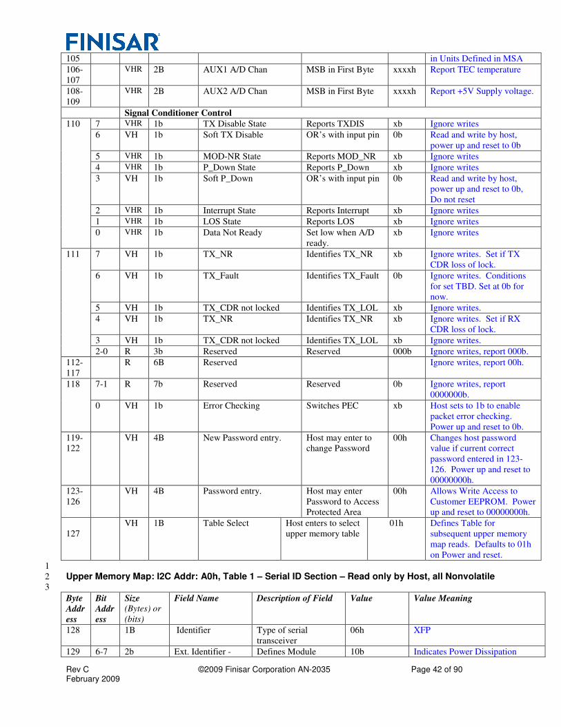
Rev C ©2009 Finisar Corporation AN-2035 Page 42 of 90 February 2009
105 in Units Defined in MSA
106-
107
VHR 2B AUX1 A/D Chan MSB in First Byte xxxxh Report TEC temperature
108-
109
VHR 2B AUX2 A/D Chan MSB in First Byte xxxxh Report +5V Supply voltage.
Signal Conditioner Control
110 7 VHR 1b TX Disable State Reports TXDIS xb Ignore writes
6 VH 1b Soft TX Disable OR’s with input pin 0b Read and write by host,
power up and reset to 0b
5 VHR 1b MOD-NR State Reports MOD_NR xb Ignore writes
4 VHR 1b P_Down State Reports P_Down xb Ignore writes
3 VH 1b Soft P_Down OR’s with input pin 0b Read and write by host,
power up and reset to 0b,
Do not reset
2 VHR 1b Interrupt State Reports Interrupt xb Ignore writes
1 VHR 1b LOS State Reports LOS xb Ignore writes
0 VHR 1b Data Not Ready Set low when A/D
ready.
xb Ignore writes
111 7 VH 1b TX_NR Identifies TX_NR xb Ignore writes. Set if TX
CDR loss of lock.
6 VH 1b TX_Fault Identifies TX_Fault 0b Ignore writes. Conditions
for set TBD. Set at 0b for
now.
5 VH 1b TX_CDR not locked Identifies TX_LOL xb Ignore writes.
4 VH 1b TX_NR Identifies TX_NR xb Ignore writes. Set if RX
CDR loss of lock.
3 VH 1b TX_CDR not locked Identifies TX_LOL xb Ignore writes.
2-0 R 3b Reserved Reserved 000b Ignore writes, report 000b.
112-
117
R 6B Reserved Ignore writes, report 00h.
118 7-1 R 7b Reserved Reserved 0b Ignore writes, report
0000000b.
0 VH 1b Error Checking Switches PEC xb Host sets to 1b to enable
packet error checking.
Power up and reset to 0b.
119-
122
VH 4B New Password entry. Host may enter to
change Password
00h Changes host password
value if current correct
password entered in 123-
126. Power up and reset to
00000000h.
123-
126
VH 4B Password entry. Host may enter
Password to Access
Protected Area
00h Allows Write Access to
Customer EEPROM. Power
up and reset to 00000000h.
127
VH 1B Table Select Host enters to select
upper memory table
01h Defines Table for
subsequent upper memory
map reads. Defaults to 01h
on Power and reset.
1
Upper Memory Map: I2C Addr: A0h, Table 1 – Serial ID Section – Read only by Host, all Nonvolatile 2
3
Byte
Addr
ess
Bit
Addr
ess
Size (Bytes) or
(bits)
Field Name Description of Field Value Value Meaning
128 1B Identifier Type of serial
transceiver
06h XFP
129 6-7 2b Ext. Identifier - Defines Module 10b Indicates Power Dissipation

Rev C ©2009 Finisar Corporation AN-2035 Page 43 of 90 February 2009
Module Power
Class
Power Class <3.5W under all specified
operating conditions.
129 5 1b Ext. Identifier -
CDR
Identifies presence of
a CDR
0b Module contains CDR function.
129 4 1b Ext. Identifier -
REFCLK
Identifies need for
REFCLK
1b Module does not need REFCLK
129 3 1b CLEI Code Present Indicates if CLEI
Code is present in
Table 2
0b To be supported on a customer
basis. Value is 1b if CLEI Code is
present in Table 2
129 0-2 3b Ext. Identifier -
Reserved
Reserved 000b
130 1B Connector Code for connector
type
07h LC
131-138 8 B Transceiver Code for electronic compatibility or optical compatibility
10 Gigabit Ethernet Compliance Codes
131 7 1b 10GBASE-SR 0b
6 1b 10GBASE-LR 0b
5 1b 10GBASE-ER 0b
4 1b Reserved 0b
3 1b 10GBASE-SW 0b
2 1b 10GBASE-LW 0b
1 1b 10GBASE-EW 0b
0 1b Reserved 0b
10 Gigabit Fibre Channel Compliance Codes
132 7 1b 1200-MX-SN-I 0b
6 1b 1200-SM-LL-L 0b
5 1b Extended reach 1550nm 0b
4 1b Intermediate reach 1310nm 0b
3 1b Reserved 0b
2 1b Reserved 0b
1 1b Reserved 0b
0 1b Reserved 0b
10 Gigabit Copper Link Compliance Codes
133 7 1b Reserved 0b
6 1b Reserved 0b
5 1b Reserved 0b
4 1b Reserved 0b
3 1b Reserved 0b
2 1b Reserved 0b
1 1b Reserved 0b
0 1b Reserved 0b
Lower Speed Link Compliance Codes
134 7 1b 1000BASE-SX/1xFC MMF 0b
6 1b 1000BASE-LX/1xFC SMF 0b
5 1b 2xFC MMF 0b
4 1b 2xFC SMF 0b
3 1b OC-48-SR 0b
2 1b OC-48-IR 0b
1 1b OC-48-LR 0b
0 1b Reserved 0b
SONET/SDH Interconnect Link Compliance Codes
135 7 1b I-64.1r 0b
6 1b I-64.1 0b
5 1b I-64.2r 0b
4 1b I-64.2 0b

Rev C ©2009 Finisar Corporation AN-2035 Page 44 of 90 February 2009
3 1b I-64.3 0b
2 1b I-64.5 0b
1 1b Reserved 0b
0 1b Reserved 0b
SONET/SDH Short Haul Link Compliance Codes
136 7 1b S-64.1 0b
6 1b S-64.2a 0b
5 1b S-64.2b 0b
4 1b S-64.3a 0b
3 1b S-64.3b 0b
2 1b S-64.5a 0b
1 1b S-64.5b 0b
0 1b Reserved 0b
SONET/SDH Long Haul Link Compliance Codes
137 7 1b L-64.1 0b
6 1b L-64.2a 0b
5 1b L-64.2b 0b
4 1b L-64.2c 0b
3 1b L-64.3 0b
2 1b G.959.1 P1L1-2D2 1b
1 1b Reserved 0b
0 1b Reserved 0b
SONET/SDH Very Long Haul Link Compliance Codes
138 7 1b V-64.2a 0b
6 1b V-64.2b 0b
5 1b V-64.3 0b
4 1b Reserved 0b
3 1b Reserved 0b
2 1b Reserved 0b
1 1b Reserved 0b
0 1b Reserved 0b
Encoding
139 7 1b 64B/66B 1b 10GE/10GFC Coding
6 1b 8B/10B 1b Not used in standards but is
supported
5 1b SONET Scrambled 1b OC-192 Coding
4 1b NRZ 1b NRZ only supported
3 1b RZ 0b
2-0 3b Reserved 000b
140 1B BR, minimum Minimum Supported
Bitrate (/100Mb)
63h 9900 Mbps
141 1B BR, maximum Maximum Supported
Bitrate (/100Mb)
6Fh 11100 Mbps for FTLX versions
10700 Mbps for FTRX versions
142 1B Length (SMF) –
km
Link length supported
for 9/125 um fiber,
units of km
50h 80km
143 1B Length (E-50um) Link length supported
for extended
bandwidth MMF,
units of 2 m
00h Not supported
144 1B Length (50m) Link length supported
for 50/125 mm fiber,
units of 1 m
00h Not supported
145 1B Length (62.5m) Link length supported
for 62.5/125 mm
00h Not supported
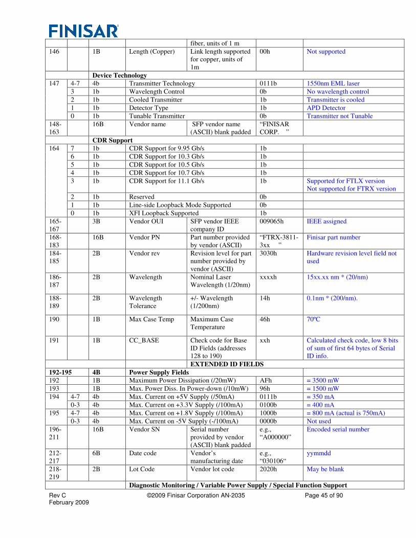
Rev C ©2009 Finisar Corporation AN-2035 Page 45 of 90 February 2009
fiber, units of 1 m
146 1B Length (Copper) Link length supported
for copper, units of
1m
00h Not supported
Device Technology
147 4-7 4b Transmitter Technology 0111b 1550nm EML laser
3 1b Wavelength Control 0b No wavelength control
2 1b Cooled Transmitter 1b Transmitter is cooled
1 1b Detector Type 1b APD Detector
0 1b Tunable Transmitter 0b Transmitter not Tunable
148-
163
16B Vendor name SFP vendor name
(ASCII) blank padded
“FINISAR
CORP. ”
CDR Support
164 7 1b CDR Support for 9.95 Gb/s 1b
6 1b CDR Support for 10.3 Gb/s 1b
5 1b CDR Support for 10.5 Gb/s 1b
4 1b CDR Support for 10.7 Gb/s 1b
3 1b CDR Support for 11.1 Gb/s 1b Supported for FTLX version
Not supported for FTRX version
2 1b Reserved 0b
1 1b Line-side Loopback Mode Supported 0b
0 1b XFI Loopback Supported 1b
165-
167
3B Vendor OUI SFP vendor IEEE
company ID
009065h IEEE assigned
168-
183
16B Vendor PN Part number provided
by vendor (ASCII)
“FTRX-3811-
3xx ”
Finisar part number
184-
185
2B Vendor rev Revision level for part
number provided by
vendor (ASCII)
3030h Hardware revision level field not
used
186-
187
2B Wavelength Nominal Laser
Wavelength (1/20nm)
xxxxh 15xx.xx nm * (20/nm)
188-
189
2B Wavelength
Tolerance
+/- Wavelength
(1/200nm)
14h 0.1nm * (200/nm).
190 1B Max Case Temp Maximum Case
Temperature
46h 70ºC
191 1B CC_BASE Check code for Base
ID Fields (addresses
128 to 190)
xxh Calculated check code, low 8 bits
of sum of first 64 bytes of Serial
ID info.
EXTENDED ID FIELDS
192-195 4B Power Supply Fields
192 1B Maximum Power Dissipation (/20mW) AFh = 3500 mW
193 1B Max. Power Diss. In Power-down (/10mW) 96h = 1500 mW
194 4-7 4b Max. Current on +5V Supply (/50mA) 0111b = 350 mA
0-3 4b Max. Current on +3.3V Supply (/100mA) 0100b = 400 mA
195 4-7 4b Max. Current on +1.8V Supply (/100mA) 1000b = 800 mA (actual is 750mA)
0-3 4b Max. Current on -5V Supply (-/100mA) 0000b Not used
196-
211
16B Vendor SN Serial number
provided by vendor
(ASCII) blank padded
e.g.,
“A000000”
Encoded serial number
212-
217
6B Date code Vendor’s
manufacturing date
e.g.,
“030106“
yymmdd
218-
219
2B Lot Code Vendor lot code 2020h May be blank
Diagnostic Monitoring / Variable Power Supply / Special Function Support
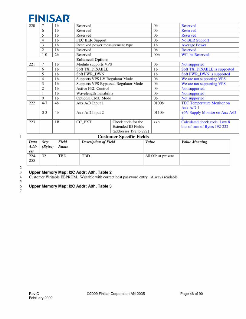
Rev C ©2009 Finisar Corporation AN-2035 Page 46 of 90 February 2009
220 7 1b Reserved 0b Reserved
6 1b Reserved 0b Reserved
5 1b Reserved 0b Reserved
4 1b FEC BER Support 0b No BER Support
3 1b Received power measurement type 1b Average Power
2 1b Reserved 0b Reserved
1-0 2b Reserved 00b Will be Reserved
Enhanced Options
221 7 1b Module supports VPS 0b Not supported
6 1b Soft TX_DISABLE 1b Soft TX_DISABLE is supported
5 1b Soft PWR_DWN 1b Soft PWR_DWN is supported
4 1b Supports VPS LV Regulator Mode 0b We are not supporting VPS
3 1b Supports VPS Bypassed Regulator Mode 0b We are not supporting VPS
2 1b Active FEC Control 0b Not supported.
1 1b Wavelength Tunability 0b Not supported
0 1b Optional CMU Mode 0b Not supported
222 4-7 4b Aux A/D Input 1 0100b TEC Temperature Monitor on
Aux A/D 1
0-3 4b Aux A/D Input 2 0110b +5V Supply Monitor on Aux A/D
2
223 1B CC_EXT Check code for the
Extended ID Fields
(addresses 192 to 222)
xxh Calculated check code. Low 8
bits of sum of Bytes 192-222
Customer Specific Fields 1
Data
Addr
ess
Size
(Bytes)
Field
Name
Description of Field Value Value Meaning
224-
255
32 TBD TBD All 00h at present
2
Upper Memory Map: I2C Addr: A0h, Table 2 3
Customer Writable EEPROM. Writable with correct host password entry. Always readable. 4
5
Upper Memory Map: I2C Addr: A0h, Table 3 6
7
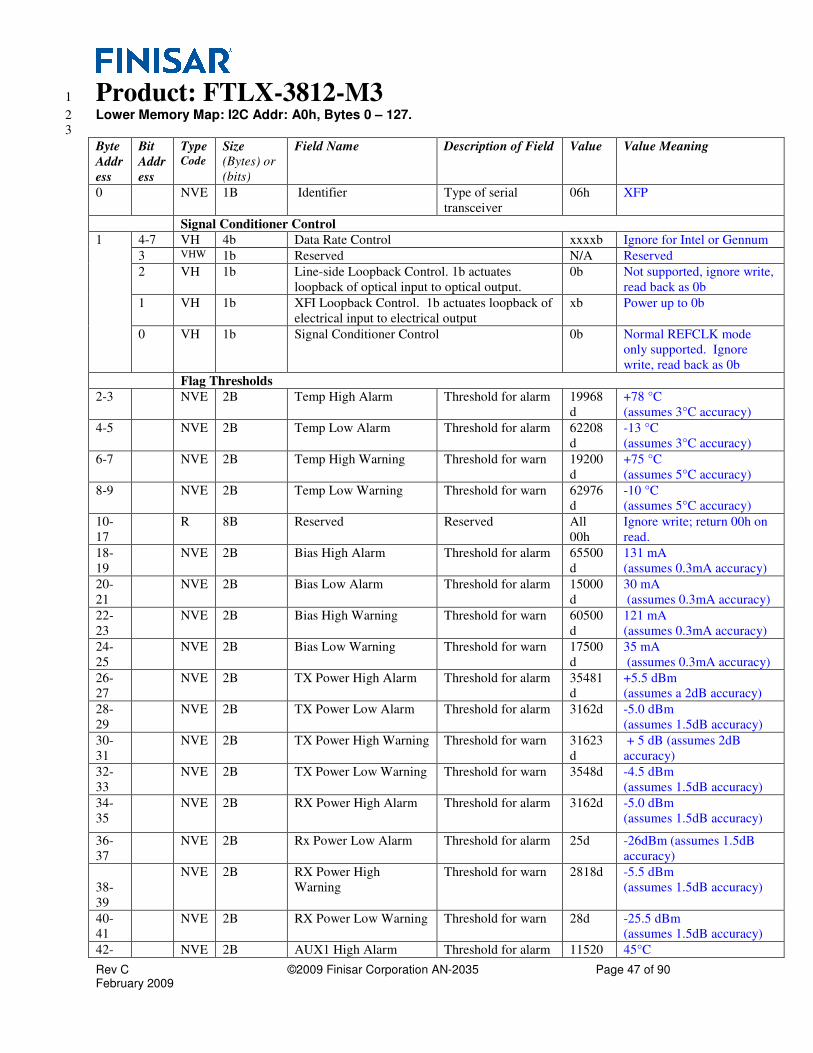
Rev C ©2009 Finisar Corporation AN-2035 Page 47 of 90 February 2009
Product: FTLX-3812-M3 1
Lower Memory Map: I2C Addr: A0h, Bytes 0 – 127. 2
3
Byte
Addr
ess
Bit
Addr
ess
Type Code
Size
(Bytes) or
(bits)
Field Name Description of Field Value Value Meaning
0 NVE 1B Identifier Type of serial
transceiver
06h XFP
Signal Conditioner Control
1 4-7 VH 4b Data Rate Control xxxxb Ignore for Intel or Gennum
3 VHW 1b Reserved N/A Reserved
2 VH 1b Line-side Loopback Control. 1b actuates
loopback of optical input to optical output.
0b Not supported, ignore write,
read back as 0b
1 VH 1b XFI Loopback Control. 1b actuates loopback of
electrical input to electrical output
xb Power up to 0b
0 VH 1b Signal Conditioner Control 0b Normal REFCLK mode
only supported. Ignore
write, read back as 0b
Flag Thresholds
2-3 NVE 2B Temp High Alarm Threshold for alarm 19968
d
+78 °C
(assumes 3°C accuracy)
4-5 NVE 2B Temp Low Alarm Threshold for alarm 62208
d
-13 °C
(assumes 3°C accuracy)
6-7 NVE 2B Temp High Warning Threshold for warn 19200
d
+75 °C
(assumes 5°C accuracy)
8-9 NVE 2B Temp Low Warning Threshold for warn 62976
d
-10 °C
(assumes 5°C accuracy)
10-
17
R 8B Reserved Reserved All
00h
Ignore write; return 00h on
read.
18-
19
NVE 2B Bias High Alarm Threshold for alarm 65500
d
131 mA
(assumes 0.3mA accuracy)
20-
21
NVE 2B Bias Low Alarm Threshold for alarm 15000
d
30 mA
(assumes 0.3mA accuracy)
22-
23
NVE 2B Bias High Warning Threshold for warn 60500
d
121 mA
(assumes 0.3mA accuracy)
24-
25
NVE 2B Bias Low Warning Threshold for warn 17500
d
35 mA
(assumes 0.3mA accuracy)
26-
27
NVE 2B TX Power High Alarm Threshold for alarm 35481
d
+5.5 dBm
(assumes a 2dB accuracy)
28-
29
NVE 2B TX Power Low Alarm Threshold for alarm 3162d -5.0 dBm
(assumes 1.5dB accuracy)
30-
31
NVE 2B TX Power High Warning Threshold for warn 31623
d
+ 5 dB (assumes 2dB
accuracy)
32-
33
NVE 2B TX Power Low Warning Threshold for warn 3548d -4.5 dBm
(assumes 1.5dB accuracy)
34-
35
NVE 2B RX Power High Alarm Threshold for alarm 3162d -5.0 dBm
(assumes 1.5dB accuracy)
36-
37
NVE 2B Rx Power Low Alarm Threshold for alarm 25d -26dBm (assumes 1.5dB
accuracy)
38-
39
NVE 2B RX Power High
Warning
Threshold for warn 2818d -5.5 dBm
(assumes 1.5dB accuracy)
40-
41
NVE 2B RX Power Low Warning Threshold for warn 28d -25.5 dBm
(assumes 1.5dB accuracy)
42- NVE 2B AUX1 High Alarm Threshold for alarm 11520 45°C
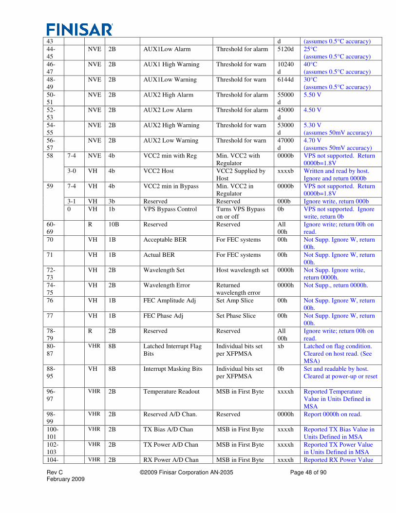
Rev C ©2009 Finisar Corporation AN-2035 Page 48 of 90 February 2009
43 d (assumes 0.5°C accuracy)
44-
45
NVE 2B AUX1Low Alarm Threshold for alarm 5120d 25°C
(assumes 0.5°C accuracy)
46-
47
NVE 2B AUX1 High Warning Threshold for warn 10240
d
40°C
(assumes 0.5°C accuracy)
48-
49
NVE 2B AUX1Low Warning Threshold for warn 6144d 30°C
(assumes 0.5°C accuracy)
50-
51
NVE 2B AUX2 High Alarm Threshold for alarm 55000
d
5.50 V
52-
53
NVE 2B AUX2 Low Alarm Threshold for alarm 45000
d
4.50 V
54-
55
NVE 2B AUX2 High Warning Threshold for warn 53000
d
5.30 V
(assumes 50mV accuracy)
56-
57
NVE 2B AUX2 Low Warning Threshold for warn 47000
d
4.70 V
(assumes 50mV accuracy)
58 7-4 NVE 4b VCC2 min with Reg Min. VCC2 with
Regulator
0000b VPS not supported. Return
0000b=1.8V
3-0 VH 4b VCC2 Host VCC2 Supplied by
Host
xxxxb Written and read by host.
Ignore and return 0000b
59 7-4 VH 4b VCC2 min in Bypass Min. VCC2 in
Regulator
0000b VPS not supported. Return
0000b=1.8V
3-1 VH 3b Reserved Reserved 000b Ignore write, return 000b
0 VH 1b VPS Bypass Control Turns VPS Bypass
on or off
0b VPS not supported. Ignore
write, return 0b
60-
69
R 10B Reserved Reserved All
00h
Ignore write; return 00h on
read.
70 VH 1B Acceptable BER For FEC systems 00h Not Supp. Ignore W, return
00h.
71 VH 1B Actual BER For FEC systems 00h Not Supp. Ignore W, return
00h.
72-
73
VH 2B Wavelength Set Host wavelength set 0000h Not Supp. Ignore write,
return 0000h.
74-
75
VH 2B Wavelength Error Returned
wavelength error
0000h Not Supp., return 0000h.
76 VH 1B FEC Amplitude Adj Set Amp Slice 00h Not Supp. Ignore W, return
00h.
77 VH 1B FEC Phase Adj Set Phase Slice 00h Not Supp. Ignore W, return
00h.
78-
79
R 2B Reserved Reserved All
00h
Ignore write; return 00h on
read.
80-
87
VHR 8B Latched Interrupt Flag
Bits
Individual bits set
per XFPMSA
xb Latched on flag condition.
Cleared on host read. (See
MSA)
88-
95
VH 8B Interrupt Masking Bits Individual bits set
per XFPMSA
0b Set and readable by host.
Cleared at power-up or reset
96-
97
VHR 2B Temperature Readout MSB in First Byte xxxxh Reported Temperature
Value in Units Defined in
MSA
98-
99
VHR 2B Reserved A/D Chan. Reserved 0000h Report 0000h on read.
100-
101
VHR 2B TX Bias A/D Chan MSB in First Byte xxxxh Reported TX Bias Value in
Units Defined in MSA
102-
103
VHR 2B TX Power A/D Chan MSB in First Byte xxxxh Reported TX Power Value
in Units Defined in MSA
104- VHR 2B RX Power A/D Chan MSB in First Byte xxxxh Reported RX Power Value
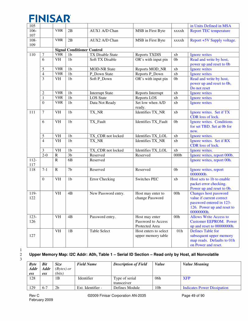
Rev C ©2009 Finisar Corporation AN-2035 Page 49 of 90 February 2009
105 in Units Defined in MSA
106-
107
VHR 2B AUX1 A/D Chan MSB in First Byte xxxxh Report TEC temperature
108-
109
VHR 2B AUX2 A/D Chan MSB in First Byte xxxxh Report +5V Supply voltage.
Signal Conditioner Control
110 7 VHR 1b TX Disable State Reports TXDIS xb Ignore writes
6 VH 1b Soft TX Disable OR’s with input pin 0b Read and write by host,
power up and reset to 0b
5 VHR 1b MOD-NR State Reports MOD_NR xb Ignore writes
4 VHR 1b P_Down State Reports P_Down xb Ignore writes
3 VH 1b Soft P_Down OR’s with input pin 0b Read and write by host,
power up and reset to 0b,
Do not reset
2 VHR 1b Interrupt State Reports Interrupt xb Ignore writes
1 VHR 1b LOS State Reports LOS xb Ignore writes
0 VHR 1b Data Not Ready Set low when A/D
ready.
xb Ignore writes
111 7 VH 1b TX_NR Identifies TX_NR xb Ignore writes. Set if TX
CDR loss of lock.
6 VH 1b TX_Fault Identifies TX_Fault 0b Ignore writes. Conditions
for set TBD. Set at 0b for
now.
5 VH 1b TX_CDR not locked Identifies TX_LOL xb Ignore writes.
4 VH 1b TX_NR Identifies TX_NR xb Ignore writes. Set if RX
CDR loss of lock.
3 VH 1b TX_CDR not locked Identifies TX_LOL xb Ignore writes.
2-0 R 3b Reserved Reserved 000b Ignore writes, report 000b.
112-
117
R 6B Reserved Ignore writes, report 00h.
118 7-1 R 7b Reserved Reserved 0b Ignore writes, report
0000000b.
0 VH 1b Error Checking Switches PEC xb Host sets to 1b to enable
packet error checking.
Power up and reset to 0b.
119-
122
VH 4B New Password entry. Host may enter to
change Password
00h Changes host password
value if current correct
password entered in 123-
126. Power up and reset to
00000000h.
123-
126
VH 4B Password entry. Host may enter
Password to Access
Protected Area
00h Allows Write Access to
Customer EEPROM. Power
up and reset to 00000000h.
127
VH 1B Table Select Host enters to select
upper memory table
01h Defines Table for
subsequent upper memory
map reads. Defaults to 01h
on Power and reset.
1
Upper Memory Map: I2C Addr: A0h, Table 1 – Serial ID Section – Read only by Host, all Nonvolatile 2
3
Byte
Addr
ess
Bit
Addr
ess
Size (Bytes) or
(bits)
Field Name Description of Field Value Value Meaning
128 1B Identifier Type of serial
transceiver
06h XFP
129 6-7 2b Ext. Identifier - Defines Module 10b Indicates Power Dissipation

Rev C ©2009 Finisar Corporation AN-2035 Page 50 of 90 February 2009
Module Power
Class
Power Class <3.5W under all specified
operating conditions.
129 5 1b Ext. Identifier -
CDR
Identifies presence of
a CDR
0b Module contains CDR function.
129 4 1b Ext. Identifier -
REFCLK
Identifies need for
REFCLK
1b Module does not need REFCLK
129 3 1b CLEI Code Present Indicates if CLEI
Code is present in
Table 2
0b To be supported on a customer
basis. Value is 1b if CLEI Code is
present in Table 2
129 0-2 3b Ext. Identifier -
Reserved
Reserved 000b
130 1B Connector Code for connector
type
07h LC
131-138 8 B Transceiver Code for electronic compatibility or optical compatibility
10 Gigabit Ethernet Compliance Codes
131 7 1b 10GBASE-SR 0b
6 1b 10GBASE-LR 0b
5 1b 10GBASE-ER 0b
4 1b Reserved 0b
3 1b 10GBASE-SW 0b
2 1b 10GBASE-LW 0b
1 1b 10GBASE-EW 0b
0 1b Reserved 0b
10 Gigabit Fibre Channel Compliance Codes
132 7 1b 1200-MX-SN-I 0b
6 1b 1200-SM-LL-L 0b
5 1b Extended reach 1550nm 0b
4 1b Intermediate reach 1310nm 0b
3 1b Reserved 0b
2 1b Reserved 0b
1 1b Reserved 0b
0 1b Reserved 0b
10 Gigabit Copper Link Compliance Codes
133 7 1b Reserved 0b
6 1b Reserved 0b
5 1b Reserved 0b
4 1b Reserved 0b
3 1b Reserved 0b
2 1b Reserved 0b
1 1b Reserved 0b
0 1b Reserved 0b
Lower Speed Link Compliance Codes
134 7 1b 1000BASE-SX/1xFC MMF 0b
6 1b 1000BASE-LX/1xFC SMF 0b
5 1b 2xFC MMF 0b
4 1b 2xFC SMF 0b
3 1b OC-48-SR 0b
2 1b OC-48-IR 0b
1 1b OC-48-LR 0b
0 1b Reserved 0b
SONET/SDH Interconnect Link Compliance Codes
135 7 1b I-64.1r 0b
6 1b I-64.1 0b
5 1b I-64.2r 0b
4 1b I-64.2 0b

Rev C ©2009 Finisar Corporation AN-2035 Page 51 of 90 February 2009
3 1b I-64.3 0b
2 1b I-64.5 0b
1 1b Reserved 0b
0 1b Reserved 0b
SONET/SDH Short Haul Link Compliance Codes
136 7 1b S-64.1 0b
6 1b S-64.2a 0b
5 1b S-64.2b 0b
4 1b S-64.3a 0b
3 1b S-64.3b 0b
2 1b S-64.5a 0b
1 1b S-64.5b 0b
0 1b Reserved 0b
SONET/SDH Long Haul Link Compliance Codes
137 7 1b L-64.1 0b
6 1b L-64.2a 0b
5 1b L-64.2b 0b
4 1b L-64.2c 0b
3 1b L-64.3 0b
2 1b G.959.1 P1L1-2D2 1b
1 1b Reserved 0b
0 1b Reserved 0b
SONET/SDH Very Long Haul Link Compliance Codes
138 7 1b V-64.2a 0b
6 1b V-64.2b 0b
5 1b V-64.3 0b
4 1b Reserved 0b
3 1b Reserved 0b
2 1b Reserved 0b
1 1b Reserved 0b
0 1b Reserved 0b
Encoding
139 7 1b 64B/66B 1b 10GE/10GFC Coding
6 1b 8B/10B 1b Not used in standards but is
supported
5 1b SONET Scrambled 1b OC-192 Coding
4 1b NRZ 1b NRZ only supported
3 1b RZ 0b
2-0 3b Reserved 000b
140 1B BR, minimum Minimum Supported
Bitrate (/100Mb)
63h 9900 Mbps
141 1B BR, maximum Maximum Supported
Bitrate (/100Mb)
6Fh 11100 Mbps for FTLX version.
10700 Mbps for FTRX version
142 1B Length (SMF) –
km
Link length supported
for 9/125 um fiber,
units of km
50h 80km
143 1B Length (E-50um) Link length supported
for extended
bandwidth MMF,
units of 2 m
00h Not supported
144 1B Length (50m) Link length supported
for 50/125 mm fiber,
units of 1 m
00h Not supported
145 1B Length (62.5m) Link length supported
for 62.5/125 mm
00h Not supported

Rev C ©2009 Finisar Corporation AN-2035 Page 52 of 90 February 2009
fiber, units of 1 m
146 1B Length (Copper) Link length supported
for copper, units of
1m
00h Not supported
Device Technology
147 4-7 4b Transmitter Technology 0111b 1550nm EML laser
3 1b Wavelength Control 0b No wavelength control
2 1b Cooled Transmitter 1b Transmitter is cooled
1 1b Detector Type 1b APD Detector
0 1b Tunable Transmitter 0b Transmitter not Tunable
148-
163
16B Vendor name SFP vendor name
(ASCII) blank padded
“FINISAR
CORP. ”
CDR Support
164 7 1b CDR Support for 9.95 Gb/s 1b
6 1b CDR Support for 10.3 Gb/s 1b
5 1b CDR Support for 10.5 Gb/s 1b
4 1b CDR Support for 10.7 Gb/s 1b
3 1b CDR Support for 11.1 Gb/s 1b Supported for FTLX version.
Not supported for FTRX version.
2 1b Reserved 0b
1 1b Line-side Loopback Mode Supported 0b
0 1b XFI Loopback Supported 1b
165-
167
3B Vendor OUI SFP vendor IEEE
company ID
009065h IEEE assigned
168-
183
16B Vendor PN Part number provided
by vendor (ASCII)
“FTLX-3812-
M3xx ”
Finisar part number
184-
185
2B Vendor rev Revision level for part
number provided by
vendor (ASCII)
3030h Hardware revision level field not
used
186-
187
2B Wavelength Nominal Laser
Wavelength (1/20nm)
xxxxh 15xx.xx nm * (20/nm)
188-
189
2B Wavelength
Tolerance
+/- Wavelength
(1/200nm)
14h 0.1nm * (200/nm).
190 1B Max Case Temp Maximum Case
Temperature
46h 70ºC
191 1B CC_BASE Check code for Base
ID Fields (addresses
128 to 190)
xxh Calculated check code, low 8 bits
of sum of first 64 bytes of Serial
ID info.
EXTENDED ID FIELDS
192-195 4B Power Supply Fields
192 1B Maximum Power Dissipation (/20mW) AFh = 3500 mW
193 1B Max. Power Diss. In Power-down (/10mW) 96h = 1500 mW
194 4-7 4b Max. Current on +5V Supply (/50mA) 0111b = 350 mA
0-3 4b Max. Current on +3.3V Supply (/100mA) 0100b = 400 mA
195 4-7 4b Max. Current on +1.8V Supply (/100mA) 1000b = 800 mA (actual is 750mA)
0-3 4b Max. Current on -5V Supply (-/100mA) 0000b Not used
196-
211
16B Vendor SN Serial number
provided by vendor
(ASCII) blank padded
e.g.,
“A000000”
Encoded serial number
212-
217
6B Date code Vendor’s
manufacturing date
e.g.,
“030106“
yymmdd
218-
219
2B Lot Code Vendor lot code 2020h May be blank
Diagnostic Monitoring / Variable Power Supply / Special Function Support
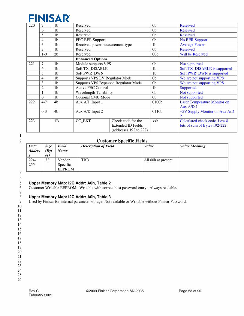
Rev C ©2009 Finisar Corporation AN-2035 Page 53 of 90 February 2009
220 7 1b Reserved 0b Reserved
6 1b Reserved 0b Reserved
5 1b Reserved 0b Reserved
4 1b FEC BER Support 0b No BER Support
3 1b Received power measurement type 1b Average Power
2 1b Reserved 0b Reserved
1-0 2b Reserved 00b Will be Reserved
Enhanced Options
221 7 1b Module supports VPS 0b Not supported
6 1b Soft TX_DISABLE 1b Soft TX_DISABLE is supported
5 1b Soft PWR_DWN 1b Soft PWR_DWN is supported
4 1b Supports VPS LV Regulator Mode 0b We are not supporting VPS
3 1b Supports VPS Bypassed Regulator Mode 0b We are not supporting VPS
2 1b Active FEC Control 1b Supported.
1 1b Wavelength Tunability 0b Not supported
0 1b Optional CMU Mode 0b Not supported
222 4-7 4b Aux A/D Input 1 0100b Laser Temperature Monitor on
Aux A/D 1
0-3 4b Aux A/D Input 2 0110b +5V Supply Monitor on Aux A/D
2
223 1B CC_EXT Check code for the
Extended ID Fields
(addresses 192 to 222)
xxh Calculated check code. Low 8
bits of sum of Bytes 192-222
1
Customer Specific Fields 2
Data
Addres
s
Size
(Byt
es)
Field
Name
Description of Field Value Value Meaning
224-
255
32 Vendor
Specific
EEPROM
TBD All 00h at present
3
4
Upper Memory Map: I2C Addr: A0h, Table 2 5
Customer Writable EEPROM. Writable with correct host password entry. Always readable. 6
7
Upper Memory Map: I2C Addr: A0h, Table 3 8
Used by Finisar for internal parameter storage. Not readable or Writable without Finisar Password. 9
10
11
12
13
14
15
16
17
18
19
20
21
22
23
24
25
26
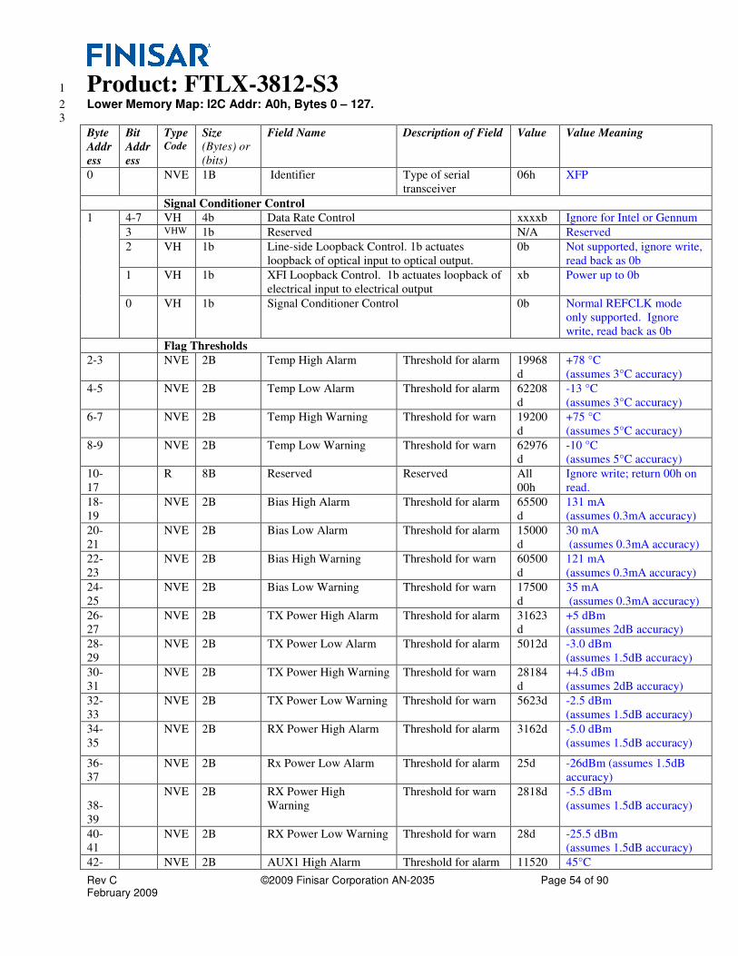
Rev C ©2009 Finisar Corporation AN-2035 Page 54 of 90 February 2009
Product: FTLX-3812-S3 1
Lower Memory Map: I2C Addr: A0h, Bytes 0 – 127. 2
3
Byte
Addr
ess
Bit
Addr
ess
Type Code
Size
(Bytes) or
(bits)
Field Name Description of Field Value Value Meaning
0 NVE 1B Identifier Type of serial
transceiver
06h XFP
Signal Conditioner Control
1 4-7 VH 4b Data Rate Control xxxxb Ignore for Intel or Gennum
3 VHW 1b Reserved N/A Reserved
2 VH 1b Line-side Loopback Control. 1b actuates
loopback of optical input to optical output.
0b Not supported, ignore write,
read back as 0b
1 VH 1b XFI Loopback Control. 1b actuates loopback of
electrical input to electrical output
xb Power up to 0b
0 VH 1b Signal Conditioner Control 0b Normal REFCLK mode
only supported. Ignore
write, read back as 0b
Flag Thresholds
2-3 NVE 2B Temp High Alarm Threshold for alarm 19968
d
+78 °C
(assumes 3°C accuracy)
4-5 NVE 2B Temp Low Alarm Threshold for alarm 62208
d
-13 °C
(assumes 3°C accuracy)
6-7 NVE 2B Temp High Warning Threshold for warn 19200
d
+75 °C
(assumes 5°C accuracy)
8-9 NVE 2B Temp Low Warning Threshold for warn 62976
d
-10 °C
(assumes 5°C accuracy)
10-
17
R 8B Reserved Reserved All
00h
Ignore write; return 00h on
read.
18-
19
NVE 2B Bias High Alarm Threshold for alarm 65500
d
131 mA
(assumes 0.3mA accuracy)
20-
21
NVE 2B Bias Low Alarm Threshold for alarm 15000
d
30 mA
(assumes 0.3mA accuracy)
22-
23
NVE 2B Bias High Warning Threshold for warn 60500
d
121 mA
(assumes 0.3mA accuracy)
24-
25
NVE 2B Bias Low Warning Threshold for warn 17500
d
35 mA
(assumes 0.3mA accuracy)
26-
27
NVE 2B TX Power High Alarm Threshold for alarm 31623
d
+5 dBm
(assumes 2dB accuracy)
28-
29
NVE 2B TX Power Low Alarm Threshold for alarm 5012d -3.0 dBm
(assumes 1.5dB accuracy)
30-
31
NVE 2B TX Power High Warning Threshold for warn 28184
d
+4.5 dBm
(assumes 2dB accuracy)
32-
33
NVE 2B TX Power Low Warning Threshold for warn 5623d -2.5 dBm
(assumes 1.5dB accuracy)
34-
35
NVE 2B RX Power High Alarm Threshold for alarm 3162d -5.0 dBm
(assumes 1.5dB accuracy)
36-
37
NVE 2B Rx Power Low Alarm Threshold for alarm 25d -26dBm (assumes 1.5dB
accuracy)
38-
39
NVE 2B RX Power High
Warning
Threshold for warn 2818d -5.5 dBm
(assumes 1.5dB accuracy)
40-
41
NVE 2B RX Power Low Warning Threshold for warn 28d -25.5 dBm
(assumes 1.5dB accuracy)
42- NVE 2B AUX1 High Alarm Threshold for alarm 11520 45°C

Rev C ©2009 Finisar Corporation AN-2035 Page 55 of 90 February 2009
43 d (assumes 0.5°C accuracy)
44-
45
NVE 2B AUX1Low Alarm Threshold for alarm 5120d 25°C
(assumes 0.5°C accuracy)
46-
47
NVE 2B AUX1 High Warning Threshold for warn 10240
d
40°C
(assumes 0.5°C accuracy)
48-
49
NVE 2B AUX1Low Warning Threshold for warn 6144d 30°C
(assumes 0.5°C accuracy)
50-
51
NVE 2B AUX2 High Alarm Threshold for alarm 55000
d
5.50 V
52-
53
NVE 2B AUX2 Low Alarm Threshold for alarm 45000
d
4.50 V
54-
55
NVE 2B AUX2 High Warning Threshold for warn 53000
d
5.30 V
(assumes 50mV accuracy)
56-
57
NVE 2B AUX2 Low Warning Threshold for warn 47000
d
4.70 V
(assumes 50mV accuracy)
58 7-4 NVE 4b VCC2 min with Reg Min. VCC2 with
Regulator
0000b VPS not supported. Return
0000b=1.8V
3-0 VH 4b VCC2 Host VCC2 Supplied by
Host
xxxxb Written and read by host.
Ignore and return 0000b
59 7-4 VH 4b VCC2 min in Bypass Min. VCC2 in
Regulator
0000b VPS not supported. Return
0000b=1.8V
3-1 VH 3b Reserved Reserved 000b Ignore write, return 000b
0 VH 1b VPS Bypass Control Turns VPS Bypass
on or off
0b VPS not supported. Ignore
write, return 0b
60-
69
R 10B Reserved Reserved All
00h
Ignore write; return 00h on
read.
70 VH 1B Acceptable BER For FEC systems 00h Not Supp. Ignore W, return
00h.
71 VH 1B Actual BER For FEC systems 00h Not Supp. Ignore W, return
00h.
72-
73
VH 2B Wavelength Set Host wavelength set 0000h Not Supp. Ignore write,
return 0000h.
74-
75
VH 2B Wavelength Error Returned
wavelength error
0000h Not Supp., return 0000h.
76 VH 1B FEC Amplitude Adj Set Amp Slice 00h Not Supp. Ignore W, return
00h.
77 VH 1B FEC Phase Adj Set Phase Slice 00h Not Supp. Ignore W, return
00h.
78-
79
R 2B Reserved Reserved All
00h
Ignore write; return 00h on
read.
80-
87
VHR 8B Latched Interrupt Flag
Bits
Individual bits set
per XFPMSA
xb Latched on flag condition.
Cleared on host read. (See
MSA)
88-
95
VH 8B Interrupt Masking Bits Individual bits set
per XFPMSA
0b Set and readable by host.
Cleared at power-up or reset
96-
97
VHR 2B Temperature Readout MSB in First Byte xxxxh Reported Temperature
Value in Units Defined in
MSA
98-
99
VHR 2B Reserved A/D Chan. Reserved 0000h Report 0000h on read.
100-
101
VHR 2B TX Bias A/D Chan MSB in First Byte xxxxh Reported TX Bias Value in
Units Defined in MSA
102-
103
VHR 2B TX Power A/D Chan MSB in First Byte xxxxh Reported TX Power Value
in Units Defined in MSA
104- VHR 2B RX Power A/D Chan MSB in First Byte xxxxh Reported RX Power Value
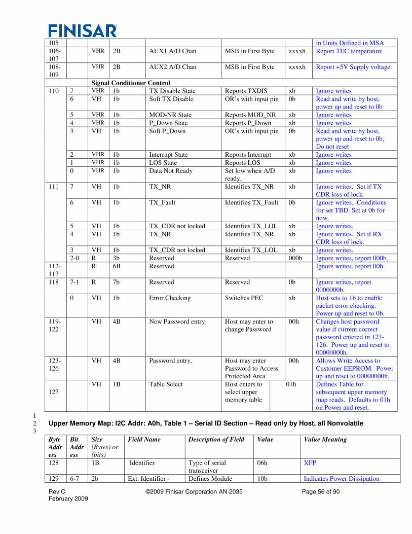
Rev C ©2009 Finisar Corporation AN-2035 Page 56 of 90 February 2009
105 in Units Defined in MSA
106-
107
VHR 2B AUX1 A/D Chan MSB in First Byte xxxxh Report TEC temperature
108-
109
VHR 2B AUX2 A/D Chan MSB in First Byte xxxxh Report +5V Supply voltage.
Signal Conditioner Control
110 7 VHR 1b TX Disable State Reports TXDIS xb Ignore writes
6 VH 1b Soft TX Disable OR’s with input pin 0b Read and write by host,
power up and reset to 0b
5 VHR 1b MOD-NR State Reports MOD_NR xb Ignore writes
4 VHR 1b P_Down State Reports P_Down xb Ignore writes
3 VH 1b Soft P_Down OR’s with input pin 0b Read and write by host,
power up and reset to 0b,
Do not reset
2 VHR 1b Interrupt State Reports Interrupt xb Ignore writes
1 VHR 1b LOS State Reports LOS xb Ignore writes
0 VHR 1b Data Not Ready Set low when A/D
ready.
xb Ignore writes
111 7 VH 1b TX_NR Identifies TX_NR xb Ignore writes. Set if TX
CDR loss of lock.
6 VH 1b TX_Fault Identifies TX_Fault 0b Ignore writes. Conditions
for set TBD. Set at 0b for
now.
5 VH 1b TX_CDR not locked Identifies TX_LOL xb Ignore writes.
4 VH 1b TX_NR Identifies TX_NR xb Ignore writes. Set if RX
CDR loss of lock.
3 VH 1b TX_CDR not locked Identifies TX_LOL xb Ignore writes.
2-0 R 3b Reserved Reserved 000b Ignore writes, report 000b.
112-
117
R 6B Reserved Ignore writes, report 00h.
118 7-1 R 7b Reserved Reserved 0b Ignore writes, report
0000000b.
0 VH 1b Error Checking Switches PEC xb Host sets to 1b to enable
packet error checking.
Power up and reset to 0b.
119-
122
VH 4B New Password entry. Host may enter to
change Password
00h Changes host password
value if current correct
password entered in 123-
126. Power up and reset to
00000000h.
123-
126
VH 4B Password entry. Host may enter
Password to Access
Protected Area
00h Allows Write Access to
Customer EEPROM. Power
up and reset to 00000000h.
127
VH 1B Table Select Host enters to
select upper
memory table
01h Defines Table for
subsequent upper memory
map reads. Defaults to 01h
on Power and reset.
1
Upper Memory Map: I2C Addr: A0h, Table 1 – Serial ID Section – Read only by Host, all Nonvolatile 2
3
Byte
Addr
ess
Bit
Addr
ess
Size (Bytes) or
(bits)
Field Name Description of Field Value Value Meaning
128 1B Identifier Type of serial
transceiver
06h XFP
129 6-7 2b Ext. Identifier - Defines Module 10b Indicates Power Dissipation

Rev C ©2009 Finisar Corporation AN-2035 Page 57 of 90 February 2009
Module Power
Class
Power Class <3.5W under all specified
operating conditions.
129 5 1b Ext. Identifier -
CDR
Identifies presence of
a CDR
0b Module contains CDR function.
129 4 1b Ext. Identifier -
REFCLK
Identifies need for
REFCLK
1b Module does not need REFCLK
129 3 1b CLEI Code Present Indicates if CLEI
Code is present in
Table 2
0b To be supported on a customer
basis. Value is 1b if CLEI Code is
present in Table 2
129 0-2 3b Ext. Identifier -
Reserved
Reserved 000b
130 1B Connector Code for connector
type
07h LC
131-138 8 B Transceiver Code for electronic compatibility or optical compatibility
10 Gigabit Ethernet Compliance Codes
131 7 1b 10GBASE-SR 0b
6 1b 10GBASE-LR 0b
5 1b 10GBASE-ER 0b
4 1b Reserved 0b
3 1b 10GBASE-SW 0b
2 1b 10GBASE-LW 0b
1 1b 10GBASE-EW 0b
0 1b Reserved 0b
10 Gigabit Fibre Channel Compliance Codes
132 7 1b 1200-MX-SN-I 0b
6 1b 1200-SM-LL-L 0b
5 1b Extended reach 1550nm 0b
4 1b Intermediate reach 1310nm 0b
3 1b Reserved 0b
2 1b Reserved 0b
1 1b Reserved 0b
0 1b Reserved 0b
10 Gigabit Copper Link Compliance Codes
133 7 1b Reserved 0b
6 1b Reserved 0b
5 1b Reserved 0b
4 1b Reserved 0b
3 1b Reserved 0b
2 1b Reserved 0b
1 1b Reserved 0b
0 1b Reserved 0b
Lower Speed Link Compliance Codes
134 7 1b 1000BASE-SX/1xFC MMF 0b
6 1b 1000BASE-LX/1xFC SMF 0b
5 1b 2xFC MMF 0b
4 1b 2xFC SMF 0b
3 1b OC-48-SR 0b
2 1b OC-48-IR 0b
1 1b OC-48-LR 0b
0 1b Reserved 0b
SONET/SDH Interconnect Link Compliance Codes
135 7 1b I-64.1r 0b
6 1b I-64.1 0b
5 1b I-64.2r 0b
4 1b I-64.2 0b
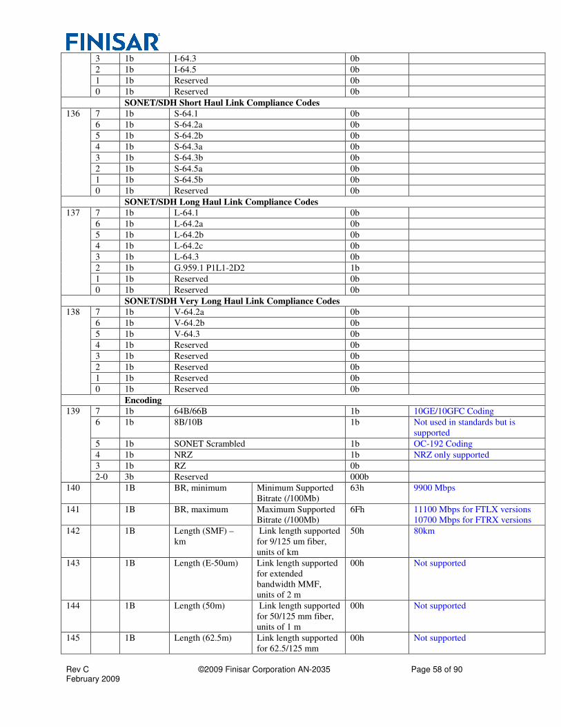
Rev C ©2009 Finisar Corporation AN-2035 Page 58 of 90 February 2009
3 1b I-64.3 0b
2 1b I-64.5 0b
1 1b Reserved 0b
0 1b Reserved 0b
SONET/SDH Short Haul Link Compliance Codes
136 7 1b S-64.1 0b
6 1b S-64.2a 0b
5 1b S-64.2b 0b
4 1b S-64.3a 0b
3 1b S-64.3b 0b
2 1b S-64.5a 0b
1 1b S-64.5b 0b
0 1b Reserved 0b
SONET/SDH Long Haul Link Compliance Codes
137 7 1b L-64.1 0b
6 1b L-64.2a 0b
5 1b L-64.2b 0b
4 1b L-64.2c 0b
3 1b L-64.3 0b
2 1b G.959.1 P1L1-2D2 1b
1 1b Reserved 0b
0 1b Reserved 0b
SONET/SDH Very Long Haul Link Compliance Codes
138 7 1b V-64.2a 0b
6 1b V-64.2b 0b
5 1b V-64.3 0b
4 1b Reserved 0b
3 1b Reserved 0b
2 1b Reserved 0b
1 1b Reserved 0b
0 1b Reserved 0b
Encoding
139 7 1b 64B/66B 1b 10GE/10GFC Coding
6 1b 8B/10B 1b Not used in standards but is
supported
5 1b SONET Scrambled 1b OC-192 Coding
4 1b NRZ 1b NRZ only supported
3 1b RZ 0b
2-0 3b Reserved 000b
140 1B BR, minimum Minimum Supported
Bitrate (/100Mb)
63h 9900 Mbps
141 1B BR, maximum Maximum Supported
Bitrate (/100Mb)
6Fh 11100 Mbps for FTLX versions
10700 Mbps for FTRX versions
142 1B Length (SMF) –
km
Link length supported
for 9/125 um fiber,
units of km
50h 80km
143 1B Length (E-50um) Link length supported
for extended
bandwidth MMF,
units of 2 m
00h Not supported
144 1B Length (50m) Link length supported
for 50/125 mm fiber,
units of 1 m
00h Not supported
145 1B Length (62.5m) Link length supported
for 62.5/125 mm
00h Not supported

Rev C ©2009 Finisar Corporation AN-2035 Page 59 of 90 February 2009
fiber, units of 1 m
146 1B Length (Copper) Link length supported
for copper, units of
1m
00h Not supported
Device Technology
147 4-7 4b Transmitter Technology 0111b 1550nm EML laser
3 1b Wavelength Control 0b No wavelength control
2 1b Cooled Transmitter 1b Transmitter is cooled
1 1b Detector Type 1b APD Detector
0 1b Tunable Transmitter 0b Transmitter not Tunable
148-
163
16B Vendor name SFP vendor name
(ASCII) blank padded
“FINISAR
CORP. ”
CDR Support
164 7 1b CDR Support for 9.95 Gb/s 1b
6 1b CDR Support for 10.3 Gb/s 1b
5 1b CDR Support for 10.5 Gb/s 1b
4 1b CDR Support for 10.7 Gb/s 1b
3 1b CDR Support for 11.1 Gb/s 1b Supported for FTLX versions.
Not supported for FTRX versions
2 1b Reserved 0b
1 1b Line-side Loopback Mode Supported 0b
0 1b XFI Loopback Supported 1b
165-
167
3B Vendor OUI SFP vendor IEEE
company ID
009065h IEEE assigned
168-
183
16B Vendor PN Part number provided
by vendor (ASCII)
“FTRX-3811-
3xx ”
Finisar part number
184-
185
2B Vendor rev Revision level for part
number provided by
vendor (ASCII)
3030h Hardware revision level field not
used
186-
187
2B Wavelength Nominal Laser
Wavelength (1/20nm)
xxxxh 15xx.xx nm * (20/nm)
188-
189
2B Wavelength
Tolerance
+/- Wavelength
(1/200nm)
14h 0.1nm * (200/nm).
190 1B Max Case Temp Maximum Case
Temperature
46h 70ºC
191 1B CC_BASE Check code for Base
ID Fields (addresses
128 to 190)
xxh Calculated check code, low 8 bits
of sum of first 64 bytes of Serial
ID info.
EXTENDED ID FIELDS
192-195 4B Power Supply Fields
192 1B Maximum Power Dissipation (/20mW) AFh = 3500 mW
193 1B Max. Power Diss. In Power-down (/10mW) 96h = 1500 mW
194 4-7 4b Max. Current on +5V Supply (/50mA) 0111b = 350 mA
0-3 4b Max. Current on +3.3V Supply (/100mA) 0100b = 400 mA
195 4-7 4b Max. Current on +1.8V Supply (/100mA) 1000b = 800 mA (actual is 750mA)
0-3 4b Max. Current on -5V Supply (-/100mA) 0000b Not used
196-
211
16B Vendor SN Serial number
provided by vendor
(ASCII) blank padded
e.g.,
“A000000”
Encoded serial number
212-
217
6B Date code Vendor’s
manufacturing date
e.g.,
“030106“
yymmdd
218-
219
2B Lot Code Vendor lot code 2020h May be blank
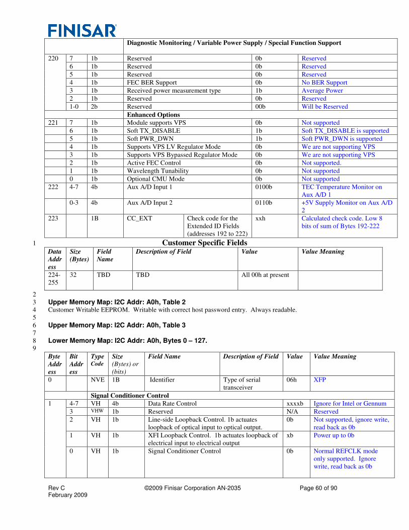
Rev C ©2009 Finisar Corporation AN-2035 Page 60 of 90 February 2009
Diagnostic Monitoring / Variable Power Supply / Special Function Support
220 7 1b Reserved 0b Reserved
6 1b Reserved 0b Reserved
5 1b Reserved 0b Reserved
4 1b FEC BER Support 0b No BER Support
3 1b Received power measurement type 1b Average Power
2 1b Reserved 0b Reserved
1-0 2b Reserved 00b Will be Reserved
Enhanced Options
221 7 1b Module supports VPS 0b Not supported
6 1b Soft TX_DISABLE 1b Soft TX_DISABLE is supported
5 1b Soft PWR_DWN 1b Soft PWR_DWN is supported
4 1b Supports VPS LV Regulator Mode 0b We are not supporting VPS
3 1b Supports VPS Bypassed Regulator Mode 0b We are not supporting VPS
2 1b Active FEC Control 0b Not supported.
1 1b Wavelength Tunability 0b Not supported
0 1b Optional CMU Mode 0b Not supported
222 4-7 4b Aux A/D Input 1 0100b TEC Temperature Monitor on
Aux A/D 1
0-3 4b Aux A/D Input 2 0110b +5V Supply Monitor on Aux A/D
2
223 1B CC_EXT Check code for the
Extended ID Fields
(addresses 192 to 222)
xxh Calculated check code. Low 8
bits of sum of Bytes 192-222
Customer Specific Fields 1
Data
Addr
ess
Size
(Bytes)
Field
Name
Description of Field Value Value Meaning
224-
255
32 TBD TBD All 00h at present
2
Upper Memory Map: I2C Addr: A0h, Table 2 3 Customer Writable EEPROM. Writable with correct host password entry. Always readable. 4
5
Upper Memory Map: I2C Addr: A0h, Table 3 6
7
Lower Memory Map: I2C Addr: A0h, Bytes 0 – 127. 8
9
Byte
Addr
ess
Bit
Addr
ess
Type Code
Size
(Bytes) or
(bits)
Field Name Description of Field Value Value Meaning
0 NVE 1B Identifier Type of serial
transceiver
06h XFP
Signal Conditioner Control
1 4-7 VH 4b Data Rate Control xxxxb Ignore for Intel or Gennum
3 VHW 1b Reserved N/A Reserved
2 VH 1b Line-side Loopback Control. 1b actuates
loopback of optical input to optical output.
0b Not supported, ignore write,
read back as 0b
1 VH 1b XFI Loopback Control. 1b actuates loopback of
electrical input to electrical output
xb Power up to 0b
0 VH 1b Signal Conditioner Control 0b Normal REFCLK mode
only supported. Ignore
write, read back as 0b
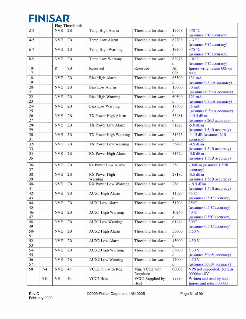
Rev C ©2009 Finisar Corporation AN-2035 Page 61 of 90 February 2009
Flag Thresholds
2-3 NVE 2B Temp High Alarm Threshold for alarm 19968
d
+78 °C
(assumes 3°C accuracy)
4-5 NVE 2B Temp Low Alarm Threshold for alarm 62208
d
-13 °C
(assumes 3°C accuracy)
6-7 NVE 2B Temp High Warning Threshold for warn 19200
d
+75 °C
(assumes 5°C accuracy)
8-9 NVE 2B Temp Low Warning Threshold for warn 62976
d
-10 °C
(assumes 5°C accuracy)
10-
17
R 8B Reserved Reserved All
00h
Ignore write; return 00h on
read.
18-
19
NVE 2B Bias High Alarm Threshold for alarm 65500
d
131 mA
(assumes 0.3mA accuracy)
20-
21
NVE 2B Bias Low Alarm Threshold for alarm 15000
d
30 mA
(assumes 0.3mA accuracy)
22-
23
NVE 2B Bias High Warning Threshold for warn 60500
d
121 mA
(assumes 0.3mA accuracy)
24-
25
NVE 2B Bias Low Warning Threshold for warn 17500
d
35 mA
(assumes 0.3mA accuracy)
26-
27
NVE 2B TX Power High Alarm Threshold for alarm 35481
d
+15.5 dBm
(assumes a 2dB accuracy)
28-
29
NVE 2B TX Power Low Alarm Threshold for alarm 3162d -5.0 dBm
(assumes 1.5dB accuracy)
30-
31
NVE 2B TX Power High Warning Threshold for warn 31623
d
+ 15 dB (assumes 2dB
accuracy)
32-
33
NVE 2B TX Power Low Warning Threshold for warn 3548d -4.5 dBm
(assumes 1.5dB accuracy)
34-
35
NVE 2B RX Power High Alarm Threshold for alarm 3162d -5.0 dBm
(assumes 1.5dB accuracy)
36-
37
NVE 2B Rx Power Low Alarm Threshold for alarm 25d -16dBm (assumes 1.5dB
accuracy)
38-
39
NVE 2B RX Power High
Warning
Threshold for warn 2818d -5.5 dBm
(assumes 1.5dB accuracy)
40-
41
NVE 2B RX Power Low Warning Threshold for warn 28d -15.5 dBm
(assumes 1.5dB accuracy)
42-
43
NVE 2B AUX1 High Alarm Threshold for alarm 11520
d
45°C
(assumes 0.5°C accuracy)
44-
45
NVE 2B AUX1Low Alarm Threshold for alarm 5120d 25°C
(assumes 0.5°C accuracy)
46-
47
NVE 2B AUX1 High Warning Threshold for warn 10240
d
40°C
(assumes 0.5°C accuracy)
48-
49
NVE 2B AUX1Low Warning Threshold for warn 6144d 30°C
(assumes 0.5°C accuracy)
50-
51
NVE 2B AUX2 High Alarm Threshold for alarm 55000
d
5.50 V
52-
53
NVE 2B AUX2 Low Alarm Threshold for alarm 45000
d
4.50 V
54-
55
NVE 2B AUX2 High Warning Threshold for warn 53000
d
5.30 V
(assumes 50mV accuracy)
56-
57
NVE 2B AUX2 Low Warning Threshold for warn 47000
d
4.70 V
(assumes 50mV accuracy)
58 7-4 NVE 4b VCC2 min with Reg Min. VCC2 with
Regulator
0000b VPS not supported. Return
0000b=1.8V
3-0 VH 4b VCC2 Host VCC2 Supplied by
Host
xxxxb Written and read by host.
Ignore and return 0000b
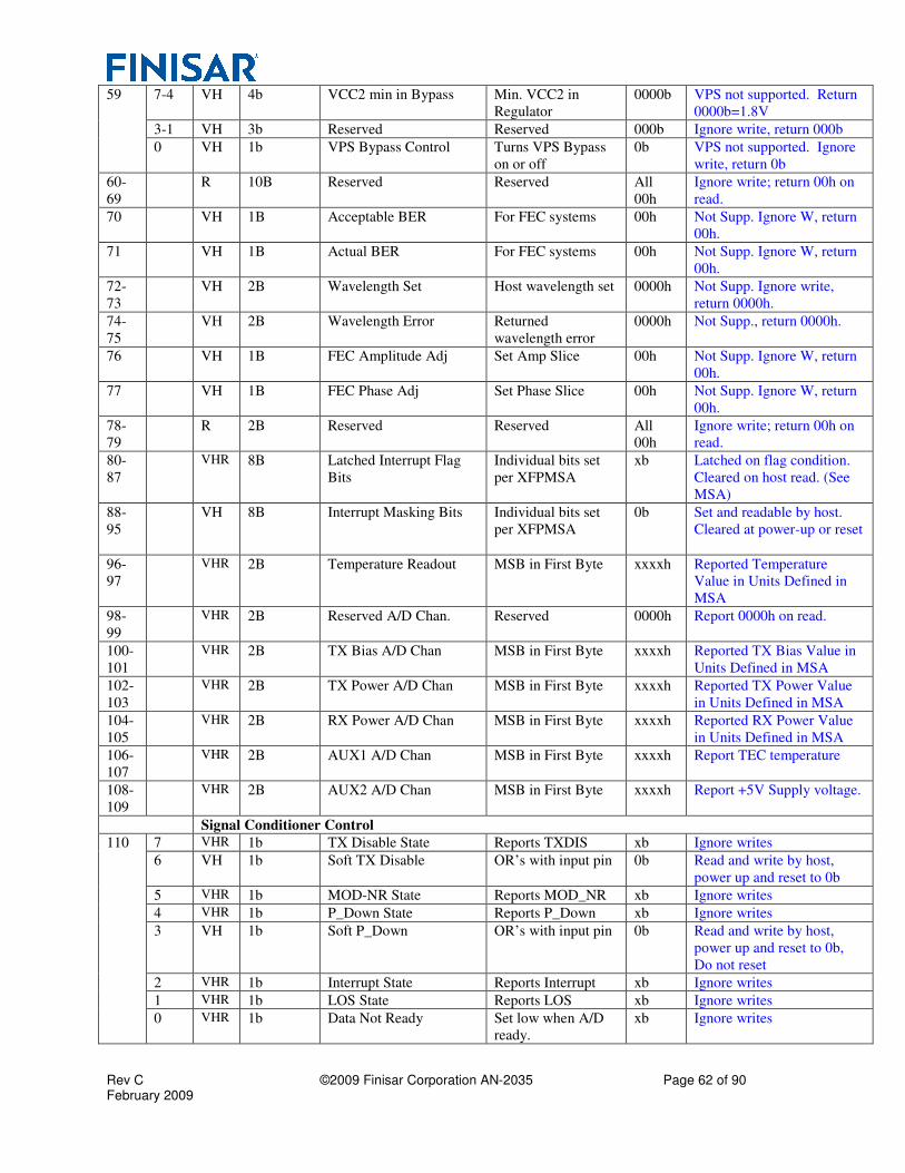
Rev C ©2009 Finisar Corporation AN-2035 Page 62 of 90 February 2009
59 7-4 VH 4b VCC2 min in Bypass Min. VCC2 in
Regulator
0000b VPS not supported. Return
0000b=1.8V
3-1 VH 3b Reserved Reserved 000b Ignore write, return 000b
0 VH 1b VPS Bypass Control Turns VPS Bypass
on or off
0b VPS not supported. Ignore
write, return 0b
60-
69
R 10B Reserved Reserved All
00h
Ignore write; return 00h on
read.
70 VH 1B Acceptable BER For FEC systems 00h Not Supp. Ignore W, return
00h.
71 VH 1B Actual BER For FEC systems 00h Not Supp. Ignore W, return
00h.
72-
73
VH 2B Wavelength Set Host wavelength set 0000h Not Supp. Ignore write,
return 0000h.
74-
75
VH 2B Wavelength Error Returned
wavelength error
0000h Not Supp., return 0000h.
76 VH 1B FEC Amplitude Adj Set Amp Slice 00h Not Supp. Ignore W, return
00h.
77 VH 1B FEC Phase Adj Set Phase Slice 00h Not Supp. Ignore W, return
00h.
78-
79
R 2B Reserved Reserved All
00h
Ignore write; return 00h on
read.
80-
87
VHR 8B Latched Interrupt Flag
Bits
Individual bits set
per XFPMSA
xb Latched on flag condition.
Cleared on host read. (See
MSA)
88-
95
VH 8B Interrupt Masking Bits Individual bits set
per XFPMSA
0b Set and readable by host.
Cleared at power-up or reset
96-
97
VHR 2B Temperature Readout MSB in First Byte xxxxh Reported Temperature
Value in Units Defined in
MSA
98-
99
VHR 2B Reserved A/D Chan. Reserved 0000h Report 0000h on read.
100-
101
VHR 2B TX Bias A/D Chan MSB in First Byte xxxxh Reported TX Bias Value in
Units Defined in MSA
102-
103
VHR 2B TX Power A/D Chan MSB in First Byte xxxxh Reported TX Power Value
in Units Defined in MSA
104-
105
VHR 2B RX Power A/D Chan MSB in First Byte xxxxh Reported RX Power Value
in Units Defined in MSA
106-
107
VHR 2B AUX1 A/D Chan MSB in First Byte xxxxh Report TEC temperature
108-
109
VHR 2B AUX2 A/D Chan MSB in First Byte xxxxh Report +5V Supply voltage.
Signal Conditioner Control
110 7 VHR 1b TX Disable State Reports TXDIS xb Ignore writes
6 VH 1b Soft TX Disable OR’s with input pin 0b Read and write by host,
power up and reset to 0b
5 VHR 1b MOD-NR State Reports MOD_NR xb Ignore writes
4 VHR 1b P_Down State Reports P_Down xb Ignore writes
3 VH 1b Soft P_Down OR’s with input pin 0b Read and write by host,
power up and reset to 0b,
Do not reset
2 VHR 1b Interrupt State Reports Interrupt xb Ignore writes
1 VHR 1b LOS State Reports LOS xb Ignore writes
0 VHR 1b Data Not Ready Set low when A/D
ready.
xb Ignore writes
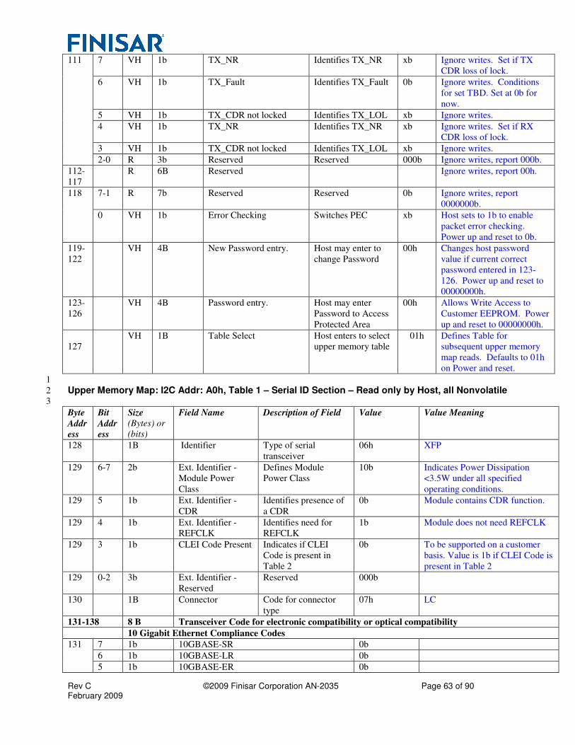
Rev C ©2009 Finisar Corporation AN-2035 Page 63 of 90 February 2009
111 7 VH 1b TX_NR Identifies TX_NR xb Ignore writes. Set if TX
CDR loss of lock.
6 VH 1b TX_Fault Identifies TX_Fault 0b Ignore writes. Conditions
for set TBD. Set at 0b for
now.
5 VH 1b TX_CDR not locked Identifies TX_LOL xb Ignore writes.
4 VH 1b TX_NR Identifies TX_NR xb Ignore writes. Set if RX
CDR loss of lock.
3 VH 1b TX_CDR not locked Identifies TX_LOL xb Ignore writes.
2-0 R 3b Reserved Reserved 000b Ignore writes, report 000b.
112-
117
R 6B Reserved Ignore writes, report 00h.
118 7-1 R 7b Reserved Reserved 0b Ignore writes, report
0000000b.
0 VH 1b Error Checking Switches PEC xb Host sets to 1b to enable
packet error checking.
Power up and reset to 0b.
119-
122
VH 4B New Password entry. Host may enter to
change Password
00h Changes host password
value if current correct
password entered in 123-
126. Power up and reset to
00000000h.
123-
126
VH 4B Password entry. Host may enter
Password to Access
Protected Area
00h Allows Write Access to
Customer EEPROM. Power
up and reset to 00000000h.
127
VH 1B Table Select Host enters to select
upper memory table
01h Defines Table for
subsequent upper memory
map reads. Defaults to 01h
on Power and reset.
1
Upper Memory Map: I2C Addr: A0h, Table 1 – Serial ID Section – Read only by Host, all Nonvolatile 2
3
Byte
Addr
ess
Bit
Addr
ess
Size
(Bytes) or
(bits)
Field Name Description of Field Value Value Meaning
128 1B Identifier Type of serial
transceiver
06h XFP
129 6-7 2b Ext. Identifier -
Module Power
Class
Defines Module
Power Class
10b Indicates Power Dissipation
<3.5W under all specified
operating conditions.
129 5 1b Ext. Identifier -
CDR
Identifies presence of
a CDR
0b Module contains CDR function.
129 4 1b Ext. Identifier -
REFCLK
Identifies need for
REFCLK
1b Module does not need REFCLK
129 3 1b CLEI Code Present Indicates if CLEI
Code is present in
Table 2
0b To be supported on a customer
basis. Value is 1b if CLEI Code is
present in Table 2
129 0-2 3b Ext. Identifier -
Reserved
Reserved 000b
130 1B Connector Code for connector
type
07h LC
131-138 8 B Transceiver Code for electronic compatibility or optical compatibility
10 Gigabit Ethernet Compliance Codes
131 7 1b 10GBASE-SR 0b
6 1b 10GBASE-LR 0b
5 1b 10GBASE-ER 0b
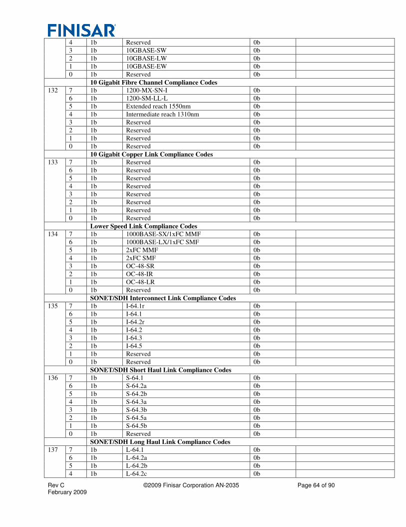
Rev C ©2009 Finisar Corporation AN-2035 Page 64 of 90 February 2009
4 1b Reserved 0b
3 1b 10GBASE-SW 0b
2 1b 10GBASE-LW 0b
1 1b 10GBASE-EW 0b
0 1b Reserved 0b
10 Gigabit Fibre Channel Compliance Codes
132 7 1b 1200-MX-SN-I 0b
6 1b 1200-SM-LL-L 0b
5 1b Extended reach 1550nm 0b
4 1b Intermediate reach 1310nm 0b
3 1b Reserved 0b
2 1b Reserved 0b
1 1b Reserved 0b
0 1b Reserved 0b
10 Gigabit Copper Link Compliance Codes
133 7 1b Reserved 0b
6 1b Reserved 0b
5 1b Reserved 0b
4 1b Reserved 0b
3 1b Reserved 0b
2 1b Reserved 0b
1 1b Reserved 0b
0 1b Reserved 0b
Lower Speed Link Compliance Codes
134 7 1b 1000BASE-SX/1xFC MMF 0b
6 1b 1000BASE-LX/1xFC SMF 0b
5 1b 2xFC MMF 0b
4 1b 2xFC SMF 0b
3 1b OC-48-SR 0b
2 1b OC-48-IR 0b
1 1b OC-48-LR 0b
0 1b Reserved 0b
SONET/SDH Interconnect Link Compliance Codes
135 7 1b I-64.1r 0b
6 1b I-64.1 0b
5 1b I-64.2r 0b
4 1b I-64.2 0b
3 1b I-64.3 0b
2 1b I-64.5 0b
1 1b Reserved 0b
0 1b Reserved 0b
SONET/SDH Short Haul Link Compliance Codes
136 7 1b S-64.1 0b
6 1b S-64.2a 0b
5 1b S-64.2b 0b
4 1b S-64.3a 0b
3 1b S-64.3b 0b
2 1b S-64.5a 0b
1 1b S-64.5b 0b
0 1b Reserved 0b
SONET/SDH Long Haul Link Compliance Codes
137 7 1b L-64.1 0b
6 1b L-64.2a 0b
5 1b L-64.2b 0b
4 1b L-64.2c 0b
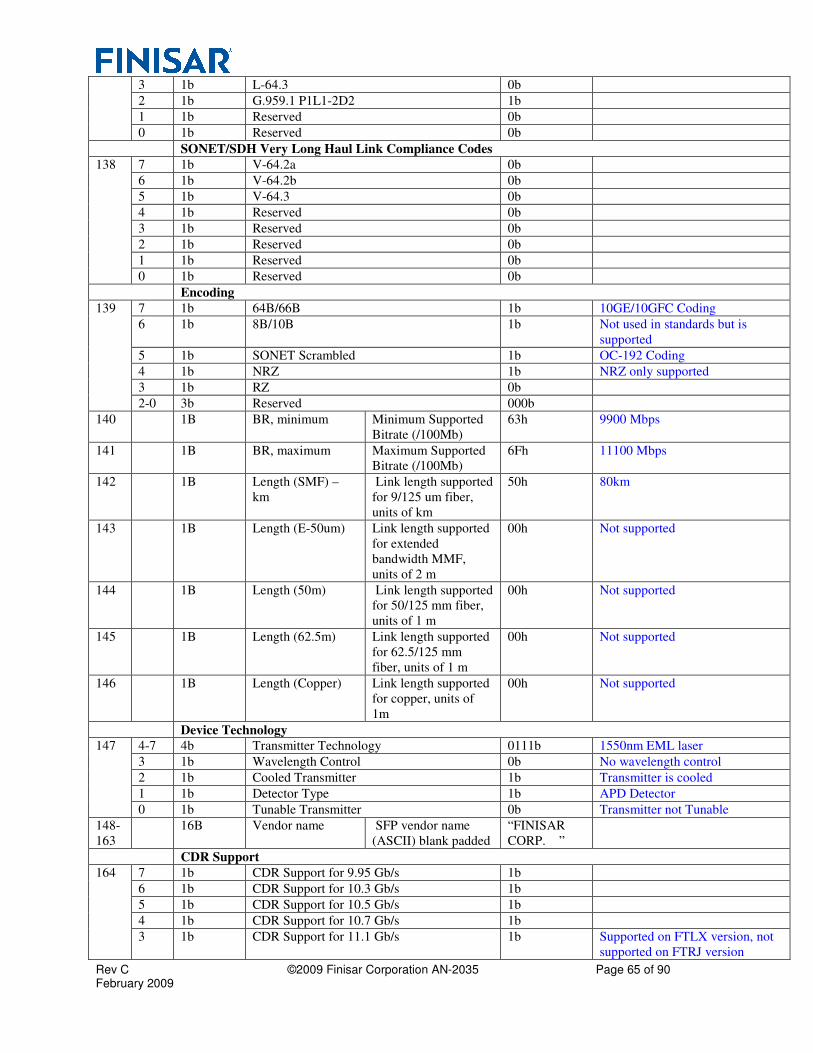
Rev C ©2009 Finisar Corporation AN-2035 Page 65 of 90 February 2009
3 1b L-64.3 0b
2 1b G.959.1 P1L1-2D2 1b
1 1b Reserved 0b
0 1b Reserved 0b
SONET/SDH Very Long Haul Link Compliance Codes
138 7 1b V-64.2a 0b
6 1b V-64.2b 0b
5 1b V-64.3 0b
4 1b Reserved 0b
3 1b Reserved 0b
2 1b Reserved 0b
1 1b Reserved 0b
0 1b Reserved 0b
Encoding
139 7 1b 64B/66B 1b 10GE/10GFC Coding
6 1b 8B/10B 1b Not used in standards but is
supported
5 1b SONET Scrambled 1b OC-192 Coding
4 1b NRZ 1b NRZ only supported
3 1b RZ 0b
2-0 3b Reserved 000b
140 1B BR, minimum Minimum Supported
Bitrate (/100Mb)
63h 9900 Mbps
141 1B BR, maximum Maximum Supported
Bitrate (/100Mb)
6Fh 11100 Mbps
142 1B Length (SMF) –
km
Link length supported
for 9/125 um fiber,
units of km
50h 80km
143 1B Length (E-50um) Link length supported
for extended
bandwidth MMF,
units of 2 m
00h Not supported
144 1B Length (50m) Link length supported
for 50/125 mm fiber,
units of 1 m
00h Not supported
145 1B Length (62.5m) Link length supported
for 62.5/125 mm
fiber, units of 1 m
00h Not supported
146 1B Length (Copper) Link length supported
for copper, units of
1m
00h Not supported
Device Technology
147 4-7 4b Transmitter Technology 0111b 1550nm EML laser
3 1b Wavelength Control 0b No wavelength control
2 1b Cooled Transmitter 1b Transmitter is cooled
1 1b Detector Type 1b APD Detector
0 1b Tunable Transmitter 0b Transmitter not Tunable
148-
163
16B Vendor name SFP vendor name
(ASCII) blank padded
“FINISAR
CORP. ”
CDR Support
164 7 1b CDR Support for 9.95 Gb/s 1b
6 1b CDR Support for 10.3 Gb/s 1b
5 1b CDR Support for 10.5 Gb/s 1b
4 1b CDR Support for 10.7 Gb/s 1b
3 1b CDR Support for 11.1 Gb/s 1b Supported on FTLX version, not
supported on FTRJ version
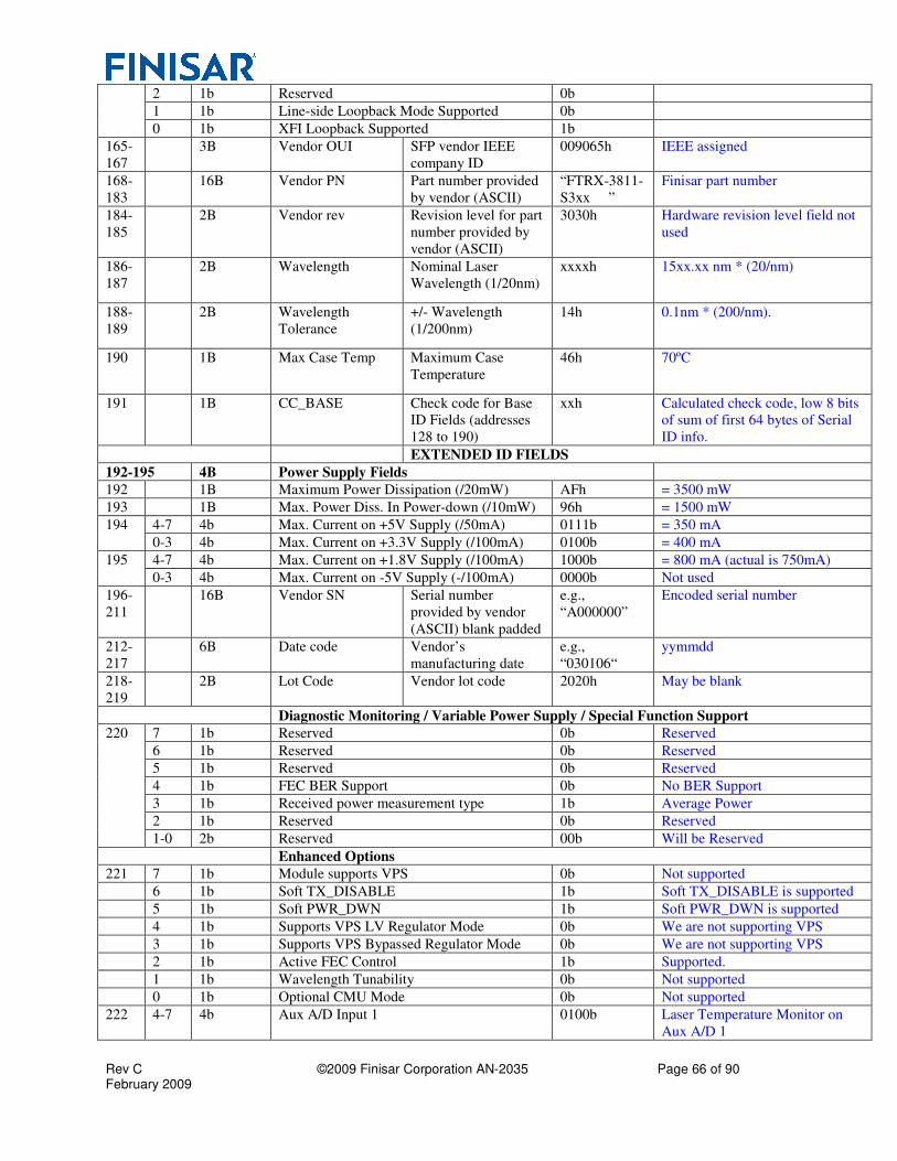
Rev C ©2009 Finisar Corporation AN-2035 Page 66 of 90 February 2009
2 1b Reserved 0b
1 1b Line-side Loopback Mode Supported 0b
0 1b XFI Loopback Supported 1b
165-
167
3B Vendor OUI SFP vendor IEEE
company ID
009065h IEEE assigned
168-
183
16B Vendor PN Part number provided
by vendor (ASCII)
“FTRX-3811-
S3xx ”
Finisar part number
184-
185
2B Vendor rev Revision level for part
number provided by
vendor (ASCII)
3030h Hardware revision level field not
used
186-
187
2B Wavelength Nominal Laser
Wavelength (1/20nm)
xxxxh 15xx.xx nm * (20/nm)
188-
189
2B Wavelength
Tolerance
+/- Wavelength
(1/200nm)
14h 0.1nm * (200/nm).
190 1B Max Case Temp Maximum Case
Temperature
46h 70ºC
191 1B CC_BASE Check code for Base
ID Fields (addresses
128 to 190)
xxh Calculated check code, low 8 bits
of sum of first 64 bytes of Serial
ID info.
EXTENDED ID FIELDS
192-195 4B Power Supply Fields
192 1B Maximum Power Dissipation (/20mW) AFh = 3500 mW
193 1B Max. Power Diss. In Power-down (/10mW) 96h = 1500 mW
194 4-7 4b Max. Current on +5V Supply (/50mA) 0111b = 350 mA
0-3 4b Max. Current on +3.3V Supply (/100mA) 0100b = 400 mA
195 4-7 4b Max. Current on +1.8V Supply (/100mA) 1000b = 800 mA (actual is 750mA)
0-3 4b Max. Current on -5V Supply (-/100mA) 0000b Not used
196-
211
16B Vendor SN Serial number
provided by vendor
(ASCII) blank padded
e.g.,
“A000000”
Encoded serial number
212-
217
6B Date code Vendor’s
manufacturing date
e.g.,
“030106“
yymmdd
218-
219
2B Lot Code Vendor lot code 2020h May be blank
Diagnostic Monitoring / Variable Power Supply / Special Function Support
220 7 1b Reserved 0b Reserved
6 1b Reserved 0b Reserved
5 1b Reserved 0b Reserved
4 1b FEC BER Support 0b No BER Support
3 1b Received power measurement type 1b Average Power
2 1b Reserved 0b Reserved
1-0 2b Reserved 00b Will be Reserved
Enhanced Options
221 7 1b Module supports VPS 0b Not supported
6 1b Soft TX_DISABLE 1b Soft TX_DISABLE is supported
5 1b Soft PWR_DWN 1b Soft PWR_DWN is supported
4 1b Supports VPS LV Regulator Mode 0b We are not supporting VPS
3 1b Supports VPS Bypassed Regulator Mode 0b We are not supporting VPS
2 1b Active FEC Control 1b Supported.
1 1b Wavelength Tunability 0b Not supported
0 1b Optional CMU Mode 0b Not supported
222 4-7 4b Aux A/D Input 1 0100b Laser Temperature Monitor on
Aux A/D 1
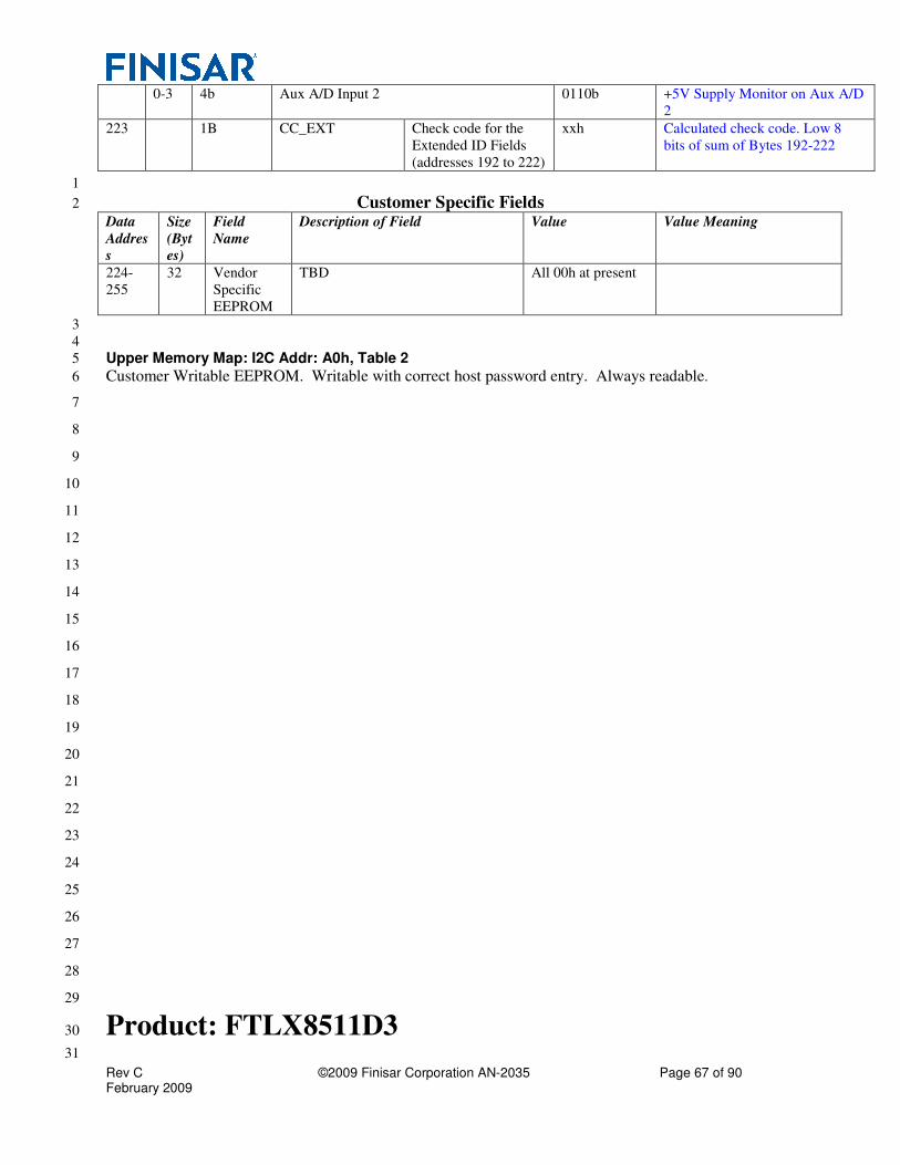
Rev C ©2009 Finisar Corporation AN-2035 Page 67 of 90 February 2009
0-3 4b Aux A/D Input 2 0110b +5V Supply Monitor on Aux A/D
2
223 1B CC_EXT Check code for the
Extended ID Fields
(addresses 192 to 222)
xxh Calculated check code. Low 8
bits of sum of Bytes 192-222
1
Customer Specific Fields 2
Data
Addres
s
Size
(Byt
es)
Field
Name
Description of Field Value Value Meaning
224-
255
32 Vendor
Specific
EEPROM
TBD All 00h at present
3
4
Upper Memory Map: I2C Addr: A0h, Table 2 5
Customer Writable EEPROM. Writable with correct host password entry. Always readable. 6
7
8
9
10
11
12
13
14
15
16
17
18
19
20
21
22
23
24
25
26
27
28
29
Product: FTLX8511D3 30
31
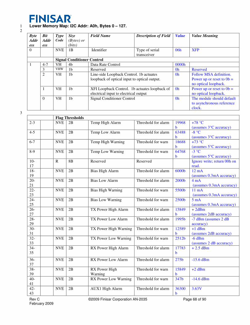
Rev C ©2009 Finisar Corporation AN-2035 Page 68 of 90 February 2009
Lower Memory Map: I2C Addr: A0h, Bytes 0 – 127. 1
2
Byte
Addr
ess
Bit
Addr
ess
Type Code
Size
(Bytes) or
(bits)
Field Name Description of Field Value Value Meaning
0 NVE 1B Identifier Type of serial
transceiver
06h XFP
Signal Conditioner Control
1 4-7 VH 4b Data Rate Control 0000h
3 VHW 1b Reserved 0h Reserved
2 VH 1b Line-side Loopback Control. 1b actuates
loopback of optical input to optical output.
0h Follow MSA definition.
Power up or reset to 0b =
no optical loopback.
1 VH 1b XFI Loopback Control. 1b actuates loopback of
electrical input to electrical output
0h Power up or reset to 0b =
no optical loopback.
0 VH 1b Signal Conditioner Control 0h The module should default
to asynchronous reference
clock.
3
Flag Thresholds
2-3 NVE 2B Temp High Alarm Threshold for alarm 19968
b
+78 °C
(assumes 3°C accuracy)
4-5 NVE 2B Temp Low Alarm Threshold for alarm 63488
b
-8 °C
(assumes 3°C accuracy)
6-7 NVE 2B Temp High Warning Threshold for warn 18688
b
+73 °C
(assumes 5°C accuracy)
8-9 NVE 2B Temp Low Warning Threshold for warn 64768
b
-3 °C
(assumes 5°C accuracy)
10-
17
R 8B Reserved Reserved Ignore write; return 00h on
read.
18-
19
NVE 2B Bias High Alarm Threshold for alarm 6000b 12 mA
(assumes 0.3mA accuracy)
20-
21
NVE 2B Bias Low Alarm Threshold for alarm 2000b 4 mA
(assumes 0.3mA accuracy)
22-
23
NVE 2B Bias High Warning Threshold for warn 5500b 11 mA
(assumes 0.3mA accuracy)
24-
25
NVE 2B Bias Low Warning Threshold for warn 2500b 5 mA
(assumes 0.3mA accuracy)
26-
27
NVE 2B TX Power High Alarm Threshold for alarm 15849
b
+ 2dBm
(assumes 2dB accuracy)
28-
29
NVE 2B TX Power Low Alarm Threshold for alarm 1995b -7 dBm (assumes 2 dB
accuracy)
30-
31
NVE 2B TX Power High Warning Threshold for warn 12589
b
+1 dBm
(assumes 2dB accuracy)
32-
33
NVE 2B TX Power Low Warning Threshold for warn 2512b -6 dBm
(assumes 2 dB accuracy)
34-
35
NVE 2B RX Power High Alarm Threshold for alarm 17783
b
+ 2.5 dBm
36-
37
NVE 2B RX Power Low Alarm Threshold for alarm 275b -15.6 dBm
38-
39
NVE 2B RX Power High
Warning
Threshold for warn 15849
b
+2 dBm
40-
41
NVE 2B RX Power Low Warning Threshold for warn 347b -14.6 dBm
42-
43
NVE 2B AUX1 High Alarm Threshold for alarm 36300
b
3.63V
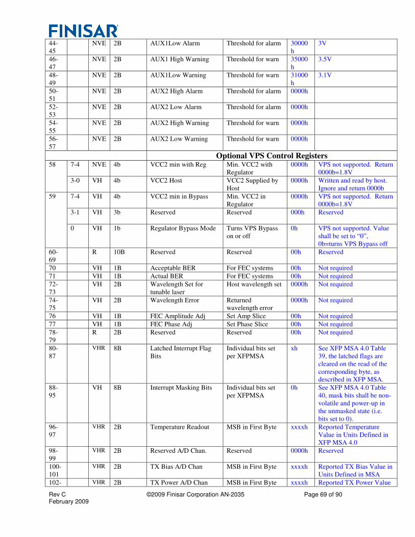
Rev C ©2009 Finisar Corporation AN-2035 Page 69 of 90 February 2009
44-
45
NVE 2B AUX1Low Alarm Threshold for alarm 30000
h
3V
46-
47
NVE 2B AUX1 High Warning Threshold for warn 35000
h
3.5V
48-
49
NVE 2B AUX1Low Warning Threshold for warn 31000
h
3.1V
50-
51
NVE 2B AUX2 High Alarm Threshold for alarm 0000h
52-
53
NVE 2B AUX2 Low Alarm Threshold for alarm 0000h
54-
55
NVE 2B AUX2 High Warning Threshold for warn 0000h
56-
57
NVE 2B AUX2 Low Warning Threshold for warn 0000h
Optional VPS Control Registers 58 7-4 NVE 4b VCC2 min with Reg Min. VCC2 with
Regulator
0000h VPS not supported. Return
0000b=1.8V
3-0 VH 4b VCC2 Host VCC2 Supplied by
Host
0000h Written and read by host.
Ignore and return 0000b
59 7-4 VH 4b VCC2 min in Bypass Min. VCC2 in
Regulator
0000h VPS not supported. Return
0000b=1.8V
3-1
VH 3b Reserved Reserved 000h Reserved
0 VH 1b Regulator Bypass Mode Turns VPS Bypass
on or off
0h VPS not supported. Value
shall be set to “0”,
0b=turns VPS Bypass off
60-
69
R 10B Reserved Reserved 00h Reserved
70 VH 1B Acceptable BER For FEC systems 00h Not required
71 VH 1B Actual BER For FEC systems 00h Not required
72-
73
VH 2B Wavelength Set for
tunable laser
Host wavelength set 0000h Not required
74-
75
VH 2B Wavelength Error Returned
wavelength error
0000h Not required
76 VH 1B FEC Amplitude Adj Set Amp Slice 00h Not required
77 VH 1B FEC Phase Adj Set Phase Slice 00h Not required
78-
79
R 2B Reserved Reserved 00h Not required
80-
87
VHR 8B Latched Interrupt Flag
Bits
Individual bits set
per XFPMSA
xh See XFP MSA 4.0 Table
39, the latched flags are
cleared on the read of the
corresponding byte, as
described in XFP MSA.
88-
95
VH 8B Interrupt Masking Bits Individual bits set
per XFPMSA
0h See XFP MSA 4.0 Table
40, mask bits shall be non-
volatile and power-up in
the unmasked state (i.e.
bits set to 0).
96-
97
VHR 2B Temperature Readout MSB in First Byte xxxxh Reported Temperature
Value in Units Defined in
XFP MSA 4.0
98-
99
VHR 2B Reserved A/D Chan. Reserved 0000h Reserved
100-
101
VHR 2B TX Bias A/D Chan MSB in First Byte xxxxh Reported TX Bias Value in
Units Defined in MSA
102- VHR 2B TX Power A/D Chan MSB in First Byte xxxxh Reported TX Power Value
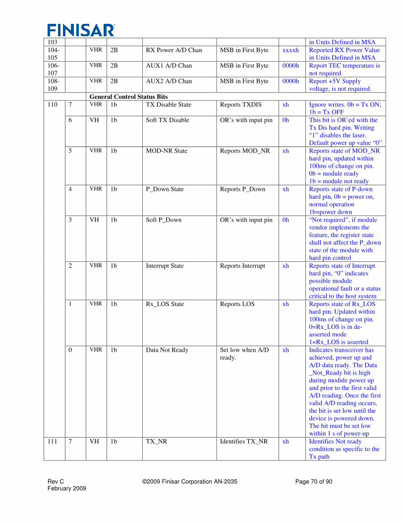
Rev C ©2009 Finisar Corporation AN-2035 Page 70 of 90 February 2009
103 in Units Defined in MSA
104-
105
VHR 2B RX Power A/D Chan MSB in First Byte xxxxh Reported RX Power Value
in Units Defined in MSA
106-
107
VHR 2B AUX1 A/D Chan MSB in First Byte 0000h Report TEC temperature is
not required
108-
109
VHR 2B AUX2 A/D Chan MSB in First Byte 0000h Report +5V Supply
voltage, is not required.
General Control Status Bits
110 7 VHR 1b TX Disable State Reports TXDIS xh Ignore writes. 0b = Tx ON;
1b = Tx OFF
6 VH 1b Soft TX Disable OR’s with input pin 0h This bit is OR’ed with the
Tx Dis hard pin. Writing
“1” disables the laser.
Default power up value “0”
5 VHR 1b MOD-NR State Reports MOD_NR xh Reports state of MOD_NR
hard pin, updated within
100ms of change on pin.
0b = module ready
1b = module not ready
4 VHR 1b P_Down State Reports P_Down xh Reports state of P-down
hard pin, 0b = power on,
normal operation
1b=power down
3 VH 1b Soft P_Down OR’s with input pin 0h “Not required”, if module
vendor implements the
feature, the register state
shall not affect the P_down
state of the module with
hard pin control
2 VHR 1b Interrupt State Reports Interrupt xh Reports state of Interrupt
hard pin, “0” indicates
possible module
operational fault or a status
critical to the host system
1 VHR 1b Rx_LOS State Reports LOS xh Reports state of Rx_LOS
hard pin. Updated within
100ms of change on pin.
0=Rx_LOS is in de-
asserted mode
1=Rx_LOS is asserted
0 VHR 1b Data Not Ready Set low when A/D
ready.
xh Indicates transceiver has
achieved, power up and
A/D data ready. The Data
_Not_Ready bit is high
during module power up
and prior to the first valid
A/D reading. Once the first
valid A/D reading occurs,
the bit is set low until the
device is powered down.
The bit must be set low
within 1 s of power-up
111 7 VH 1b TX_NR Identifies TX_NR xh Identifies Not ready
condition as specific to the
Tx path
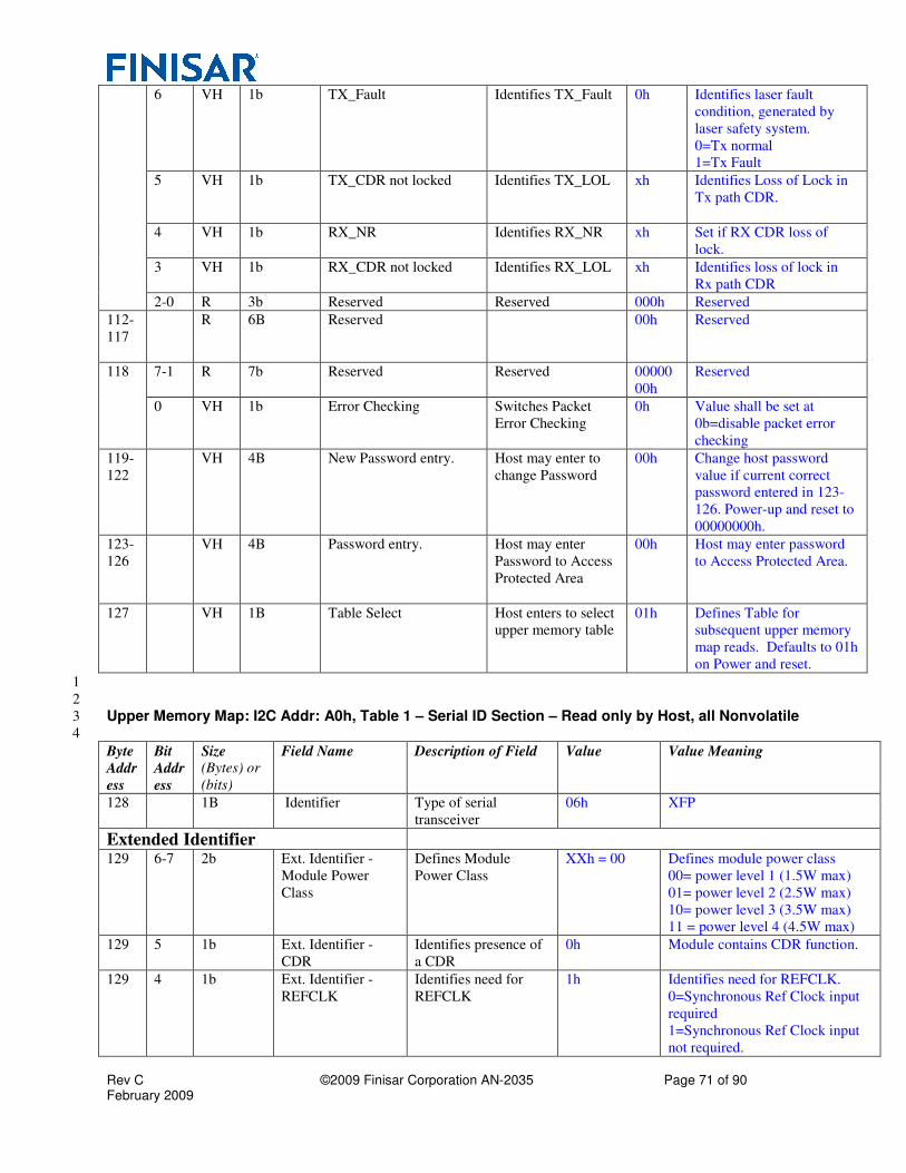
Rev C ©2009 Finisar Corporation AN-2035 Page 71 of 90 February 2009
6 VH 1b TX_Fault Identifies TX_Fault 0h Identifies laser fault
condition, generated by
laser safety system.
0=Tx normal
1=Tx Fault
5 VH 1b TX_CDR not locked Identifies TX_LOL xh Identifies Loss of Lock in
Tx path CDR.
4 VH 1b RX_NR Identifies RX_NR xh Set if RX CDR loss of
lock.
3 VH 1b RX_CDR not locked Identifies RX_LOL xh Identifies loss of lock in
Rx path CDR
2-0 R 3b Reserved Reserved 000h Reserved
112-
117
R 6B Reserved 00h Reserved
118 7-1 R 7b Reserved Reserved 00000
00h
Reserved
0 VH 1b Error Checking Switches Packet
Error Checking
0h Value shall be set at
0b=disable packet error
checking
119-
122
VH 4B New Password entry. Host may enter to
change Password
00h Change host password
value if current correct
password entered in 123-
126. Power-up and reset to
00000000h.
123-
126
VH 4B Password entry. Host may enter
Password to Access
Protected Area
00h Host may enter password
to Access Protected Area.
127
VH 1B Table Select Host enters to select
upper memory table
01h Defines Table for
subsequent upper memory
map reads. Defaults to 01h
on Power and reset.
1
2
Upper Memory Map: I2C Addr: A0h, Table 1 – Serial ID Section – Read only by Host, all Nonvolatile 3
4
Byte
Addr
ess
Bit
Addr
ess
Size (Bytes) or
(bits)
Field Name Description of Field Value Value Meaning
128 1B Identifier Type of serial
transceiver
06h XFP
Extended Identifier
129 6-7 2b Ext. Identifier -
Module Power
Class
Defines Module
Power Class
XXh = 00 Defines module power class
00= power level 1 (1.5W max)
01= power level 2 (2.5W max)
10= power level 3 (3.5W max)
11 = power level 4 (4.5W max)
129 5 1b Ext. Identifier -
CDR
Identifies presence of
a CDR
0h Module contains CDR function.
129 4 1b Ext. Identifier -
REFCLK
Identifies need for
REFCLK
1h Identifies need for REFCLK.
0=Synchronous Ref Clock input
required
1=Synchronous Ref Clock input
not required.
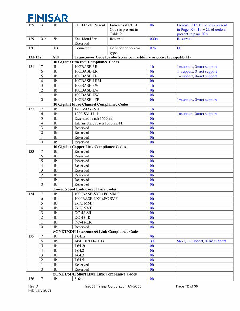
Rev C ©2009 Finisar Corporation AN-2035 Page 72 of 90 February 2009
129 3 1b CLEI Code Present Indicates if CLEI
Code is present in
Table 2
0h Indicate if CLEI code is present
in Page 02h, 1b = CLEI code is
present in page 02h
129 0-2 3b Ext. Identifier -
Reserved
Reserved 000h Reserved
130 1B Connector Code for connector
type
07h LC
131-138 8 B Transceiver Code for electronic compatibility or optical compatibility
10 Gigabit Ethernet Compliance Codes
131 7 1b 10GBASE-SR 1h 1=support, 0=not support
6 1b 10GBASE-LR 0h 1=support, 0=not support
5 1b 10GBASE-ER 0h 1=support, 0=not support
4 1b 10GBASE-LRM 0h
3 1b 10GBASE-SW 1h
2 1b 10GBASE-LW 0h
1 1b 10GBASE-EW 0h
0 1b 10GBASE - ZR 0h 1=support, 0=not support
10 Gigabit Fibre Channel Compliance Codes
132 7 1b 1200-MX-SN-I 1h
6 1b 1200-SM-LL-L 0h 1=support, 0=not support
5 1b Extended reach 1550nm 0h
4 1b Intermediate reach 1310nm FP 0h
3 1b Reserved 0h
2 1b Reserved 0h
1 1b Reserved 0h
0 1b Reserved 0h
10 Gigabit Copper Link Compliance Codes
133 7 1b Reserved 0h
6 1b Reserved 0h
5 1b Reserved 0h
4 1b Reserved 0h
3 1b Reserved 0h
2 1b Reserved 0h
1 1b Reserved 0h
0 1b Reserved 0h
Lower Speed Link Compliance Codes
134 7 1b 1000BASE-SX/1xFC MMF 0h
6 1b 1000BASE-LX/1xFC SMF 0h
5 1b 2xFC MMF 0h
4 1b 2xFC SMF 0h
3 1b OC-48-SR 0h
2 1b OC-48-IR 0h
1 1b OC-48-LR 0h
0 1b Reserved 0h
SONET/SDH Interconnect Link Compliance Codes
135 7 1b I-64.1r 0h
6 1b I-64.1 (P111-2D1) Xh SR-1, 1=support, 0=no support
5 1b I-64.2r 0h
4 1b I-64.2 0h
3 1b I-64.3 0h
2 1b I-64.5 0h
1 1b Reserved 0h
0 1b Reserved 0h
SONET/SDH Short Haul Link Compliance Codes
136 7 1b S-64.1 0h
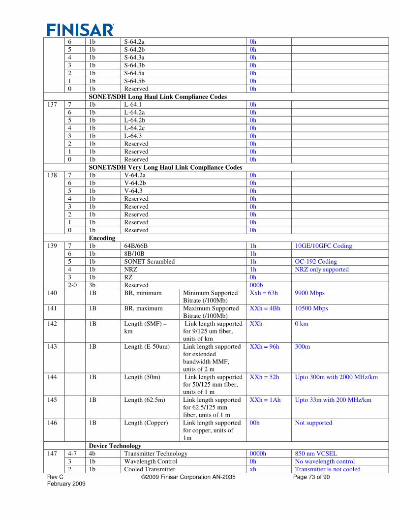
Rev C ©2009 Finisar Corporation AN-2035 Page 73 of 90 February 2009
6 1b S-64.2a 0h
5 1b S-64.2b 0h
4 1b S-64.3a 0h
3 1b S-64.3b 0h
2 1b S-64.5a 0h
1 1b S-64.5b 0h
0 1b Reserved 0h
SONET/SDH Long Haul Link Compliance Codes
137 7 1b L-64.1 0h
6 1b L-64.2a 0h
5 1b L-64.2b 0h
4 1b L-64.2c 0h
3 1b L-64.3 0h
2 1b Reserved 0h
1 1b Reserved 0h
0 1b Reserved 0h
SONET/SDH Very Long Haul Link Compliance Codes
138 7 1b V-64.2a 0h
6 1b V-64.2b 0h
5 1b V-64.3 0h
4 1b Reserved 0h
3 1b Reserved 0h
2 1b Reserved 0h
1 1b Reserved 0h
0 1b Reserved 0h
Encoding
139 7 1b 64B/66B 1h 10GE/10GFC Coding
6 1b 8B/10B 1h
5 1b SONET Scrambled 1h OC-192 Coding
4 1b NRZ 1h NRZ only supported
3 1b RZ 0h
2-0 3b Reserved 000b
140 1B BR, minimum Minimum Supported
Bitrate (/100Mb)
Xxh = 63h 9900 Mbps
141 1B BR, maximum Maximum Supported
Bitrate (/100Mb)
XXh = 4Bh 10500 Mbps
142 1B Length (SMF) –
km
Link length supported
for 9/125 um fiber,
units of km
XXh 0 km
143 1B Length (E-50um) Link length supported
for extended
bandwidth MMF,
units of 2 m
XXh = 96h 300m
144 1B Length (50m) Link length supported
for 50/125 mm fiber,
units of 1 m
XXh = 52h Upto 300m with 2000 MHz/km
145 1B Length (62.5m) Link length supported
for 62.5/125 mm
fiber, units of 1 m
XXh = 1Ah Upto 33m with 200 MHz/km
146 1B Length (Copper) Link length supported
for copper, units of
1m
00h Not supported
Device Technology
147 4-7 4b Transmitter Technology 0000h 850 nm VCSEL
3 1b Wavelength Control 0h No wavelength control
2 1b Cooled Transmitter xh Transmitter is not cooled
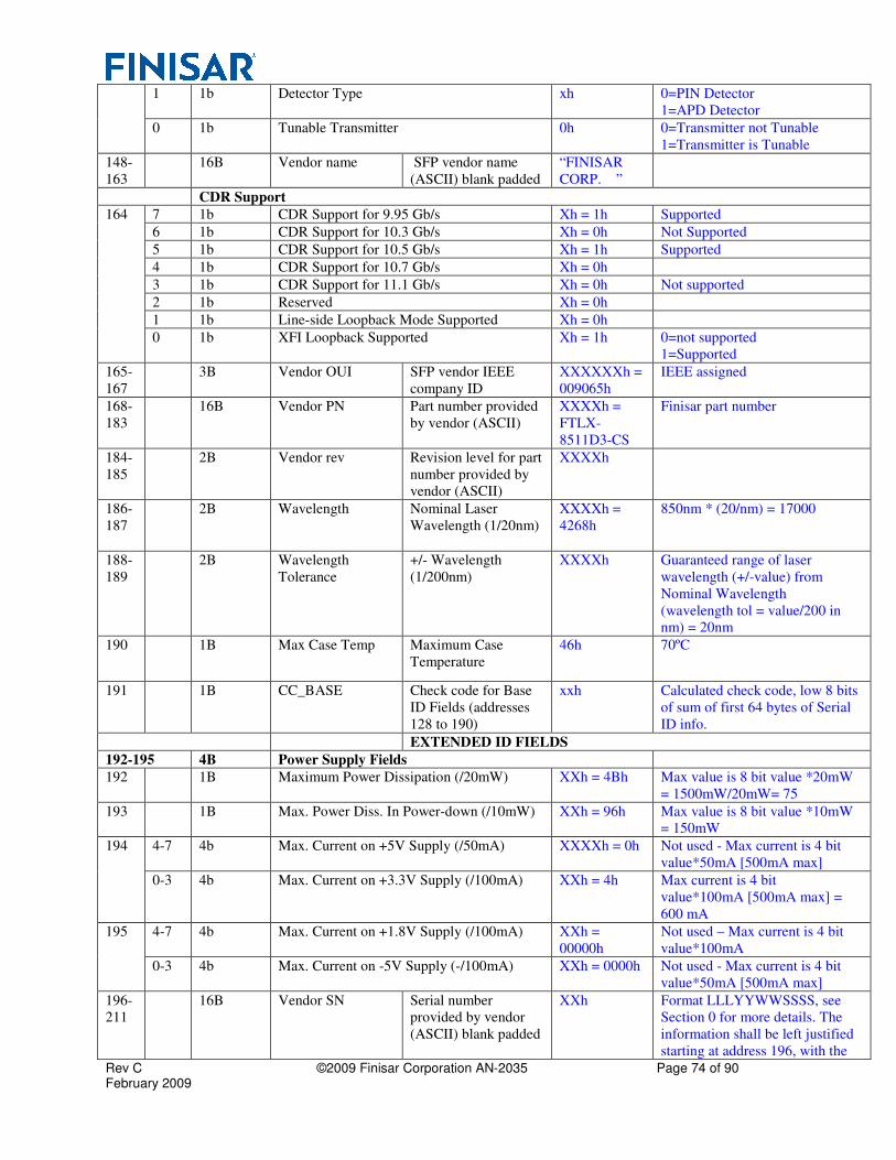
Rev C ©2009 Finisar Corporation AN-2035 Page 74 of 90 February 2009
1 1b Detector Type xh 0=PIN Detector
1=APD Detector
0 1b Tunable Transmitter 0h 0=Transmitter not Tunable
1=Transmitter is Tunable
148-
163
16B Vendor name SFP vendor name
(ASCII) blank padded
“FINISAR
CORP. ”
CDR Support
164 7 1b CDR Support for 9.95 Gb/s Xh = 1h Supported
6 1b CDR Support for 10.3 Gb/s Xh = 0h Not Supported
5 1b CDR Support for 10.5 Gb/s Xh = 1h Supported
4 1b CDR Support for 10.7 Gb/s Xh = 0h
3 1b CDR Support for 11.1 Gb/s Xh = 0h Not supported
2 1b Reserved Xh = 0h
1 1b Line-side Loopback Mode Supported Xh = 0h
0 1b XFI Loopback Supported Xh = 1h 0=not supported
1=Supported
165-
167
3B Vendor OUI SFP vendor IEEE
company ID
XXXXXXh =
009065h
IEEE assigned
168-
183
16B Vendor PN Part number provided
by vendor (ASCII)
XXXXh =
FTLX-
8511D3-CS
Finisar part number
184-
185
2B Vendor rev Revision level for part
number provided by
vendor (ASCII)
XXXXh
186-
187
2B Wavelength Nominal Laser
Wavelength (1/20nm)
XXXXh =
4268h
850nm * (20/nm) = 17000
188-
189
2B Wavelength
Tolerance
+/- Wavelength
(1/200nm)
XXXXh Guaranteed range of laser
wavelength (+/-value) from
Nominal Wavelength
(wavelength tol = value/200 in
nm) = 20nm
190 1B Max Case Temp Maximum Case
Temperature
46h 70ºC
191 1B CC_BASE Check code for Base
ID Fields (addresses
128 to 190)
xxh Calculated check code, low 8 bits
of sum of first 64 bytes of Serial
ID info.
EXTENDED ID FIELDS
192-195 4B Power Supply Fields
192 1B Maximum Power Dissipation (/20mW) XXh = 4Bh Max value is 8 bit value *20mW
= 1500mW/20mW= 75
193 1B Max. Power Diss. In Power-down (/10mW) XXh = 96h Max value is 8 bit value *10mW
= 150mW
194 4-7 4b Max. Current on +5V Supply (/50mA) XXXXh = 0h Not used - Max current is 4 bit
value*50mA [500mA max]
0-3 4b Max. Current on +3.3V Supply (/100mA) XXh = 4h Max current is 4 bit
value*100mA [500mA max] =
600 mA
195 4-7 4b Max. Current on +1.8V Supply (/100mA) XXh =
00000h
Not used – Max current is 4 bit
value*100mA
0-3 4b Max. Current on -5V Supply (-/100mA) XXh = 0000h Not used - Max current is 4 bit
value*50mA [500mA max]
196-
211
16B Vendor SN Serial number
provided by vendor
(ASCII) blank padded
XXh Format LLLYYWWSSSS, see
Section 0 for more details. The
information shall be left justified
starting at address 196, with the
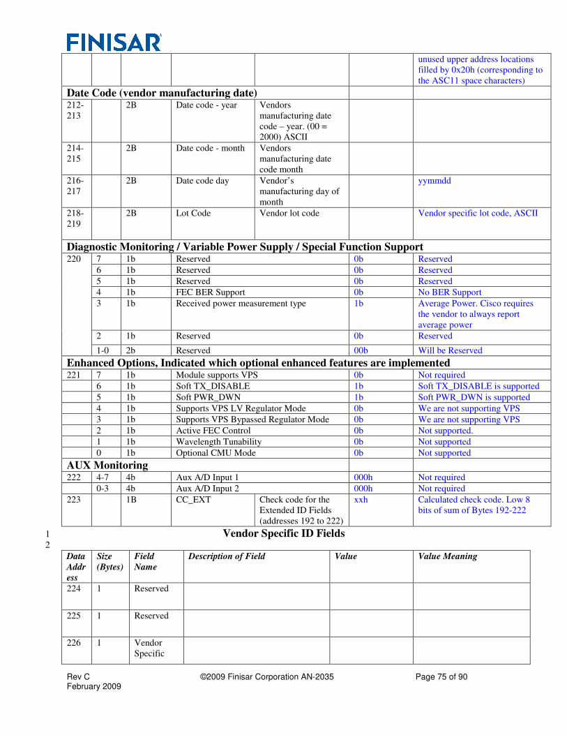
Rev C ©2009 Finisar Corporation AN-2035 Page 75 of 90 February 2009
unused upper address locations
filled by 0x20h (corresponding to
the ASC11 space characters)
Date Code (vendor manufacturing date)
212-
213
2B Date code - year Vendors
manufacturing date
code – year. (00 =
2000) ASCII
214-
215
2B Date code - month Vendors
manufacturing date
code month
216-
217
2B Date code day Vendor’s
manufacturing day of
month
yymmdd
218-
219
2B Lot Code Vendor lot code Vendor specific lot code, ASCII
Diagnostic Monitoring / Variable Power Supply / Special Function Support 220 7 1b Reserved 0b Reserved
6 1b Reserved 0b Reserved
5 1b Reserved 0b Reserved
4 1b FEC BER Support 0b No BER Support
3 1b Received power measurement type 1b Average Power. Cisco requires
the vendor to always report
average power
2 1b Reserved 0b Reserved
1-0 2b Reserved 00b Will be Reserved
Enhanced Options, Indicated which optional enhanced features are implemented 221 7 1b Module supports VPS 0b Not required
6 1b Soft TX_DISABLE 1b Soft TX_DISABLE is supported
5 1b Soft PWR_DWN 1b Soft PWR_DWN is supported
4 1b Supports VPS LV Regulator Mode 0b We are not supporting VPS
3 1b Supports VPS Bypassed Regulator Mode 0b We are not supporting VPS
2 1b Active FEC Control 0b Not supported.
1 1b Wavelength Tunability 0b Not supported
0 1b Optional CMU Mode 0b Not supported
AUX Monitoring
222 4-7 4b Aux A/D Input 1 000h Not required
0-3 4b Aux A/D Input 2 000h Not required
223 1B CC_EXT Check code for the
Extended ID Fields
(addresses 192 to 222)
xxh Calculated check code. Low 8
bits of sum of Bytes 192-222
Vendor Specific ID Fields 1
2
Data
Addr
ess
Size
(Bytes)
Field
Name
Description of Field Value Value Meaning
224 1 Reserved
225 1 Reserved
226 1 Vendor
Specific
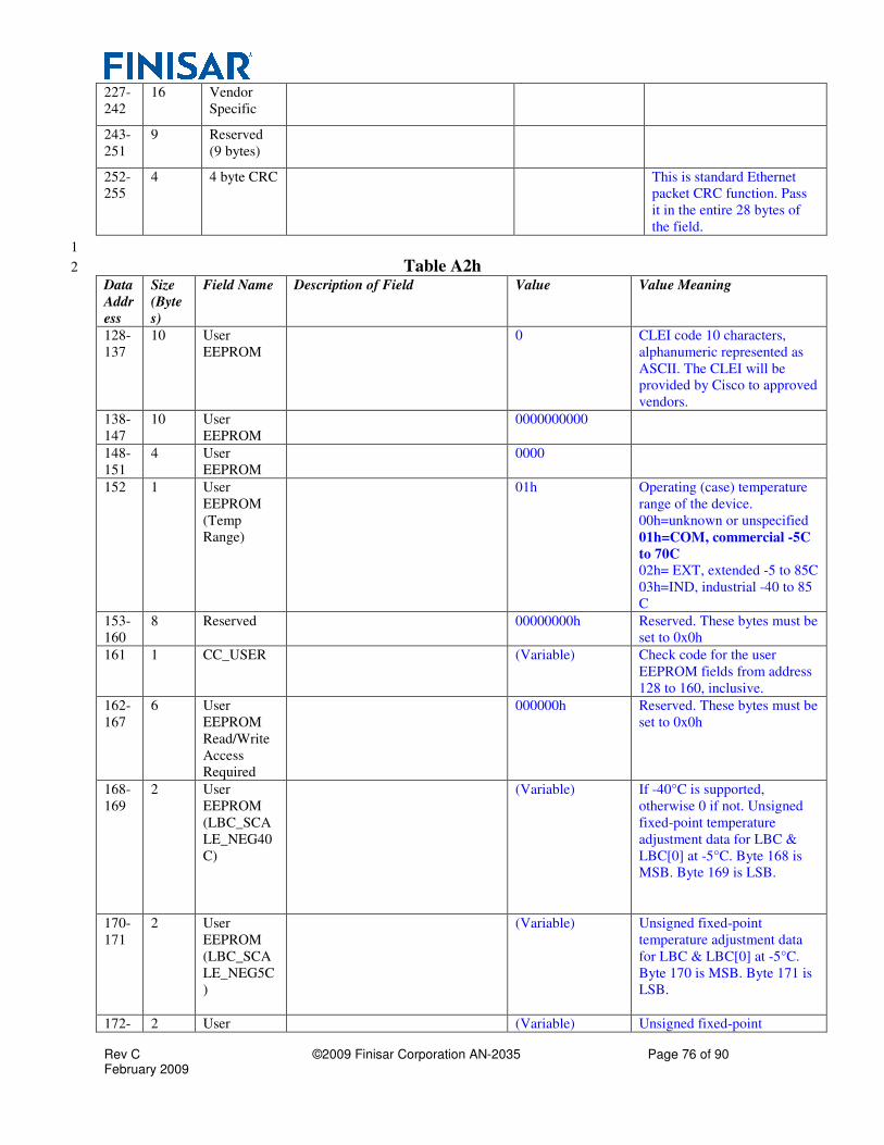
Rev C ©2009 Finisar Corporation AN-2035 Page 76 of 90 February 2009
227-
242
16 Vendor
Specific
243-
251
9 Reserved
(9 bytes)
252-
255
4 4 byte CRC This is standard Ethernet
packet CRC function. Pass
it in the entire 28 bytes of
the field.
1
Table A2h 2
Data
Addr
ess
Size
(Byte
s)
Field Name Description of Field Value Value Meaning
128-
137
10 User
EEPROM
0 CLEI code 10 characters,
alphanumeric represented as
ASCII. The CLEI will be
provided by Cisco to approved
vendors.
138-
147
10 User
EEPROM
0000000000
148-
151
4 User
EEPROM
0000
152 1 User
EEPROM
(Temp
Range)
01h Operating (case) temperature
range of the device.
00h=unknown or unspecified
01h=COM, commercial -5C
to 70C
02h= EXT, extended -5 to 85C
03h=IND, industrial -40 to 85
C
153-
160
8 Reserved 00000000h Reserved. These bytes must be
set to 0x0h
161 1 CC_USER (Variable) Check code for the user
EEPROM fields from address
128 to 160, inclusive.
162-
167
6 User
EEPROM
Read/Write
Access
Required
000000h Reserved. These bytes must be
set to 0x0h
168-
169
2 User
EEPROM
(LBC_SCA
LE_NEG40
C)
(Variable) If -40°C is supported,
otherwise 0 if not. Unsigned
fixed-point temperature
adjustment data for LBC &
LBC[0] at -5°C. Byte 168 is
MSB. Byte 169 is LSB.
170-
171
2 User
EEPROM
(LBC_SCA
LE_NEG5C
)
(Variable) Unsigned fixed-point
temperature adjustment data
for LBC & LBC[0] at -5°C.
Byte 170 is MSB. Byte 171 is
LSB.
172- 2 User (Variable) Unsigned fixed-point
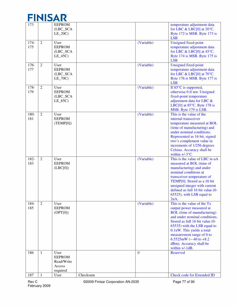
Rev C ©2009 Finisar Corporation AN-2035 Page 77 of 90 February 2009
173 EEPROM
(LBC_SCA
LE_20C)
temperature adjustment data
for LBC & LBC[0] at 20°C.
Byte 172 is MSB. Byte 173 is
LSB
174-
175
2 User
EEPROM
(LBC_SCA
LE_45C)
(Variable) Unsigned fixed-point
temperature adjustment data
for LBC & LBC[0] at 45°C.
Byte 174 is MSB. Byte 175 is
LSB
176-
177
2 User
EEPROM
(LBC_SCA
LE_70C)
(Variable) Unsigned fixed-point
temperature adjustment data
for LBC & LBC[0] at 70°C.
Byte 176 is MSB. Byte 177 is
LSB
178-
179
2 User
EEPROM
(LBC_SCA
LE_85C)
(Variable) If 85°C is supported,
otherwise 0 if not. Unsigned
fixed-point temperature
adjustment data for LBC &
LBC[0] at 85°C. Byte 178 is
MSB. Byte 179 is LSB.
180-
181
2 User
EEPROM
(TEMP[0])
(Variable) This is the value of the
internal transceiver
temperature measured at BOL
(time of manufacturing) and
under nominal conditions.
Represented as 16 bit, signed
two’s complement value in
increments of 1/256 degrees
Celsius. Accuracy shall be
within +/-3°C
182-
183
2 User
EEPROM
(LBC[0])
(Variable) This is the value of LBC in uA
measured at BOL (time of
manufacturing) and under
nominal conditions at
transceiver temperature of
TEMP[0]. Stored as a 16 bit
unsigned integer with current
defined as full 16 bit value (0-
65525), with LSB equal to
2uA.
184-
185
2 User
EEPROM
(OPT[0])
(Variable) This is the value of the Tx
output power measured at
BOL (time of manufacturing)
and under nominal conditions.
Stored as full 16 bit value (0-
65535) with the LSB equal to
0.1uW. This yields a total
measurement range of 0 to
6.5525mW (~-40 to +8.2
dBm). Accuracy shall be
within +/-1dB.
186 1 User
EEPROM
Read/Write
Access
required
0 Reserved
187 1 User Checksum Check code for Extended ID
Rev C ©2009 Finisar Corporation AN-2035 Page 78 of 90 February 2009
EEPROM
CC_Vendor
fields from addresses 162 to
186, inclusive
188-
189
2 User
EEPROM
(OPR[0]
Read/Write
Access
required
0 Module vendor shall write
0x0h into these bytes at time
of manufacturing.
190 1 User
EEPROM
Read/Write
Access
Required
00b Reserved.
191 1 User
EEPROM
Read/Write
access
required
Check sum
variable
Check code for Extended ID
fields from addresses 188 to
190.
192-
211
20 User
EEPROM
Read/write
access
required
0b
212-
222
11 User
EEPROM
Read/Write
Access
Required
0b Reserved
223 1B CC_EXT Check code for
the Extended ID
Fields
(addresses 192
to 222)
xxh Calculated check code. Low 8
bits of sum of Bytes 192-222
Customer Specific Fields 1
Data
Addres
s
Size
(Byt
es)
Field
Name
Description of Field Value Value Meaning
224-
255
32 Vendor
Specific
EEPROM
TBD All 00h at present
2
3
Upper Memory Map: I2C Addr: A0h, Table 2 4
Customer Writable EEPROM. Writable with correct host password entry. Always readable. 5
6
7
Product: FTLX4213_4 channel 8
Lower Memory Map: I2C Addr: A0h, Bytes 0 – 127. 9
10
Byte
Addr
ess
Bit
Addr
ess
Type Code
Size
(Bytes) or
(bits)
Field Name Description of Field Value Value Meaning
0 NVE 1B Identifier Type of serial 06h XFP
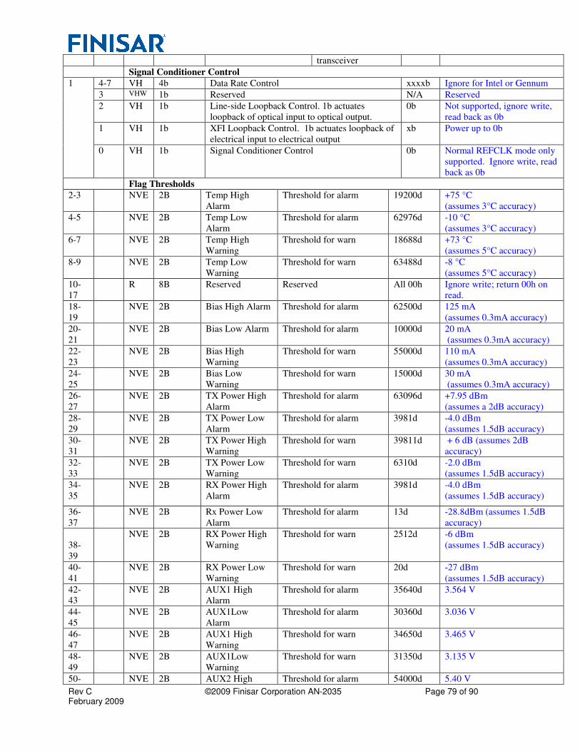
Rev C ©2009 Finisar Corporation AN-2035 Page 79 of 90 February 2009
transceiver
Signal Conditioner Control
1 4-7 VH 4b Data Rate Control xxxxb Ignore for Intel or Gennum
3 VHW 1b Reserved N/A Reserved
2 VH 1b Line-side Loopback Control. 1b actuates
loopback of optical input to optical output.
0b Not supported, ignore write,
read back as 0b
1 VH 1b XFI Loopback Control. 1b actuates loopback of
electrical input to electrical output
xb Power up to 0b
0 VH 1b Signal Conditioner Control 0b Normal REFCLK mode only
supported. Ignore write, read
back as 0b
Flag Thresholds
2-3 NVE 2B Temp High
Alarm
Threshold for alarm 19200d +75 °C
(assumes 3°C accuracy)
4-5 NVE 2B Temp Low
Alarm
Threshold for alarm 62976d -10 °C
(assumes 3°C accuracy)
6-7 NVE 2B Temp High
Warning
Threshold for warn 18688d +73 °C
(assumes 5°C accuracy)
8-9 NVE 2B Temp Low
Warning
Threshold for warn 63488d -8 °C
(assumes 5°C accuracy)
10-
17
R 8B Reserved Reserved All 00h Ignore write; return 00h on
read.
18-
19
NVE 2B Bias High Alarm Threshold for alarm 62500d 125 mA
(assumes 0.3mA accuracy)
20-
21
NVE 2B Bias Low Alarm Threshold for alarm 10000d 20 mA
(assumes 0.3mA accuracy)
22-
23
NVE 2B Bias High
Warning
Threshold for warn 55000d 110 mA
(assumes 0.3mA accuracy)
24-
25
NVE 2B Bias Low
Warning
Threshold for warn 15000d 30 mA
(assumes 0.3mA accuracy)
26-
27
NVE 2B TX Power High
Alarm
Threshold for alarm 63096d +7.95 dBm
(assumes a 2dB accuracy)
28-
29
NVE 2B TX Power Low
Alarm
Threshold for alarm 3981d -4.0 dBm
(assumes 1.5dB accuracy)
30-
31
NVE 2B TX Power High
Warning
Threshold for warn 39811d + 6 dB (assumes 2dB
accuracy)
32-
33
NVE 2B TX Power Low
Warning
Threshold for warn 6310d -2.0 dBm
(assumes 1.5dB accuracy)
34-
35
NVE 2B RX Power High
Alarm
Threshold for alarm 3981d -4.0 dBm
(assumes 1.5dB accuracy)
36-
37
NVE 2B Rx Power Low
Alarm
Threshold for alarm 13d -28.8dBm (assumes 1.5dB
accuracy)
38-
39
NVE 2B RX Power High
Warning
Threshold for warn 2512d -6 dBm
(assumes 1.5dB accuracy)
40-
41
NVE 2B RX Power Low
Warning
Threshold for warn 20d -27 dBm
(assumes 1.5dB accuracy)
42-
43
NVE 2B AUX1 High
Alarm
Threshold for alarm 35640d 3.564 V
44-
45
NVE 2B AUX1Low
Alarm
Threshold for alarm 30360d 3.036 V
46-
47
NVE 2B AUX1 High
Warning
Threshold for warn 34650d 3.465 V
48-
49
NVE 2B AUX1Low
Warning
Threshold for warn 31350d 3.135 V
50- NVE 2B AUX2 High Threshold for alarm 54000d 5.40 V
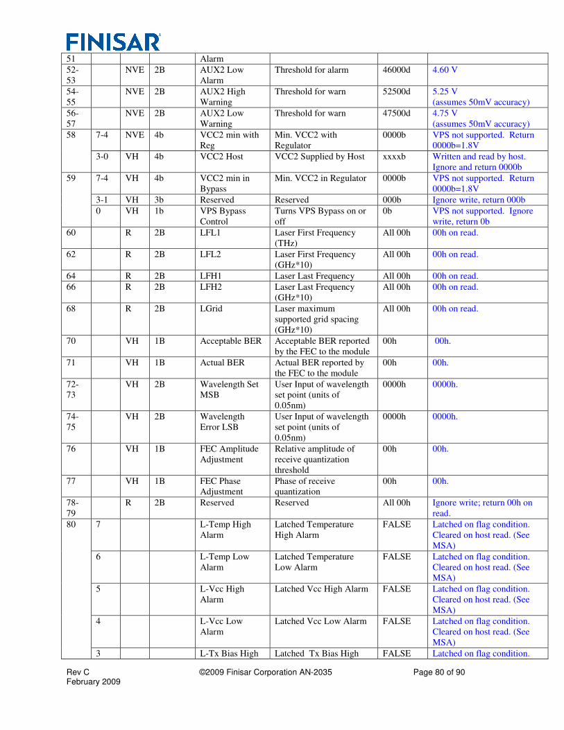
Rev C ©2009 Finisar Corporation AN-2035 Page 80 of 90 February 2009
51 Alarm
52-
53
NVE 2B AUX2 Low
Alarm
Threshold for alarm 46000d 4.60 V
54-
55
NVE 2B AUX2 High
Warning
Threshold for warn 52500d 5.25 V
(assumes 50mV accuracy)
56-
57
NVE 2B AUX2 Low
Warning
Threshold for warn 47500d 4.75 V
(assumes 50mV accuracy)
58 7-4 NVE 4b VCC2 min with
Reg
Min. VCC2 with
Regulator
0000b VPS not supported. Return
0000b=1.8V
3-0 VH 4b VCC2 Host VCC2 Supplied by Host xxxxb Written and read by host.
Ignore and return 0000b
59 7-4 VH 4b VCC2 min in
Bypass
Min. VCC2 in Regulator 0000b VPS not supported. Return
0000b=1.8V
3-1 VH 3b Reserved Reserved 000b Ignore write, return 000b
0 VH 1b VPS Bypass
Control
Turns VPS Bypass on or
off
0b VPS not supported. Ignore
write, return 0b
60 R 2B LFL1 Laser First Frequency
(THz)
All 00h 00h on read.
62 R 2B LFL2 Laser First Frequency
(GHz*10)
All 00h 00h on read.
64 R 2B LFH1 Laser Last Frequency All 00h 00h on read.
66 R 2B LFH2 Laser Last Frequency
(GHz*10)
All 00h 00h on read.
68 R 2B LGrid Laser maximum
supported grid spacing
(GHz*10)
All 00h 00h on read.
70 VH 1B Acceptable BER Acceptable BER reported
by the FEC to the module
00h 00h.
71 VH 1B Actual BER Actual BER reported by
the FEC to the module
00h 00h.
72-
73
VH 2B Wavelength Set
MSB
User Input of wavelength
set point (units of
0.05nm)
0000h 0000h.
74-
75
VH 2B Wavelength
Error LSB
User Input of wavelength
set point (units of
0.05nm)
0000h 0000h.
76 VH 1B FEC Amplitude
Adjustment
Relative amplitude of
receive quantization
threshold
00h 00h.
77 VH 1B FEC Phase
Adjustment
Phase of receive
quantization
00h 00h.
78-
79
R 2B Reserved Reserved All 00h Ignore write; return 00h on
read.
80 7 L-Temp High
Alarm
Latched Temperature
High Alarm
FALSE Latched on flag condition.
Cleared on host read. (See
MSA)
6 L-Temp Low
Alarm
Latched Temperature
Low Alarm
FALSE Latched on flag condition.
Cleared on host read. (See
MSA)
5 L-Vcc High
Alarm
Latched Vcc High Alarm FALSE Latched on flag condition.
Cleared on host read. (See
MSA)
4 L-Vcc Low
Alarm
Latched Vcc Low Alarm FALSE Latched on flag condition.
Cleared on host read. (See
MSA)
3 L-Tx Bias High Latched Tx Bias High FALSE Latched on flag condition.
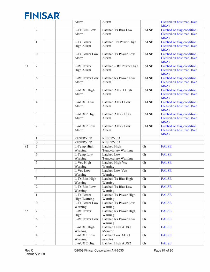
Rev C ©2009 Finisar Corporation AN-2035 Page 81 of 90 February 2009
Alarm Alarm Cleared on host read. (See
MSA)
2 L-Tx Bias Low
Alarm
Latched Tx Bias Low
Alarm
FALSE Latched on flag condition.
Cleared on host read. (See
MSA)
1 L-Tx Power
High Alarm
Latched Tx Power High
Alarm
FALSE Latched on flag condition.
Cleared on host read. (See
MSA)
0 L-Tx Power Low
Alarm
Latched Tx Power Low
Alarm
FALSE Latched on flag condition.
Cleared on host read. (See
MSA)
81 7 L-Rx Power
High Alarm
Latched – Rx Power High
Alarm
FALSE Latched on flag condition.
Cleared on host read. (See
MSA)
6 L-Rx Power Low
Alarm
Latched Rx Power Low
Alarm
FALSE Latched on flag condition.
Cleared on host read. (See
MSA)
5 L-AUX1 High
Alarm
Latched AUX 1 High
Alarm
FALSE Latched on flag condition.
Cleared on host read. (See
MSA)
4 L-AUX1 Low
Alarm
Latched AUX1 Low
Alarm
FALSE Latched on flag condition.
Cleared on host read. (See
MSA)
3 L-AUX 2 High
Alarm
Latched AUX2 High
Alarm
FALSE Latched on flag condition.
Cleared on host read. (See
MSA)
2 L-AUX 2 Low
Alarm
Latched AUX2 Low
Alarm
FALSE Latched on flag condition.
Cleared on host read. (See
MSA)
1 RESERVED RESERVED
0 RESERVED RESERVED
82 7 L-Temp High
Warning
Latched High
Temperature Warning
0h FALSE
6 L-Temp Low
Warning
Latched Low
Temperature Warning
0h FALSE
5 L-Vcc High
Warning
Latched High Vcc
Warning
0h FALSE
4 L-Vcc Low
Warning
Latched Low Vcc
Warning
0h FALSE
3 L-Tx Bias High
Warning
Latched Tx Bias High
Warning
0h FALSE
2 L-Tx Bias Low
Warning
Latched Tx Bias Low
Warning
0h FALSE
1 L-Tx Power
High Warning
Latched Tx Power High
Warning
0h FALSE
0 L-Tx Power Low
Warning
Latched Tx Power Low
Warning
0h FALSE
83 7 L-Rx Power
High
Latched Rx Power High
Warning
0h FALSE
6 L-Rx Power Low Latched Rx Power Low
Warning
0h FALSE
5 L-AUX1 High
Warning
Latched High AUX1
Monitor
0h FALSE
4 L-AUX 1 Low
Warning
Latched Low AUX1
monitor
0h FALSE
3 L-AUX 2 High Latched High AUX2 0h FALSE
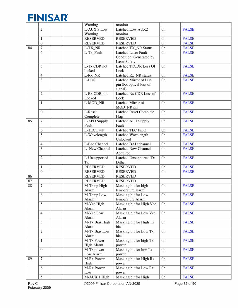
Rev C ©2009 Finisar Corporation AN-2035 Page 82 of 90 February 2009
Warning monitor
2 L-AUX 3 Low
Warning
Latched Low AUX2
monitor
0h FALSE
1 RESERVED RESERVED 0h FALSE
0 RESERVED RESERVED 0h FALSE
84 7 L-TX_NR Latched TX_NR Status 0h FALSE
6 L-Tx_Fault Latched Laser Fault
Condition. Generated by
Laser Safety
0h FALSE
5 L-Tx CDR not
locked
Latched TxCDR Loss Of
Lock
0h FALSE
4 L-Rx_NR Latched Rx_NR status 0h FALSE
3 L-LOS Latched Mirror of LOS
pin (Rx optical loss of
signal)
0h FALSE
2 L-Rx CDR not
Locked
Latched Rx CDR Loss of
Lock
0h FALSE
1 L-MOD_NR Latched Mirror of
MOD_NR pin
0h FALSE
0 L-Reset
Complete
Latched Reset Complete
Flag
0h FALSE
85 7 L-APD Supply
Fault
Latched APD Supply
Fault
0h FALSE
6 L-TEC Fault Latched TEC Fault 0h FALSE
5 L-Wavelength Latched Wavelength
Unlocked
0h FALSE
4 L-Bad Channel Latched BAD channel 0h FALSE
3 L- New Channel Latched New Channel
Acquired
0h FALSE
2 L-Unsupported
Tx
Latched Unsupported Tx
Dither
0h FALSE
1 RESERVED RESERVED 0h FALSE
0 RESERVED RESERVED 0h FALSE
86 RESERVED RESERVED
87 RESERVED RESERVED
88 7 M-Temp High
Alarm
Masking bit for high
temperature alarm
0h FALSE
6 M-Temp Low
Alarm
Masking bit for Low
temperature Alarm
0h FALSE
5 M-Vcc High
Alarm
Masking bit for High Vcc
Alarm
0h FALSE
4 M-Vcc Low
Alarm
Masking bit for Low Vcc
Alarm
0h FALSE
3 M-Tx Bias High
Alarm
Masking bit for High Tx
bias
0h FALSE
2 M-Tx Bias Low
Alarm
Masking bit for Low Tx
bias
0h FALSE
1 M-Tx Power
High Alarm
Masking bit for high Tx
power
0h FALSE
0 M-Tx power
Low Alarm
Masking bit for low Tx
power
0h FALSE
89 7 M-Rx Power
High
Masking bit for High Rx
power
0h FALSE
6 M-Rx Power
Low
Masking bit for Low Rx
power
0h FALSE
5 M-AUX 1 High Masking bit for High 0h FALSE
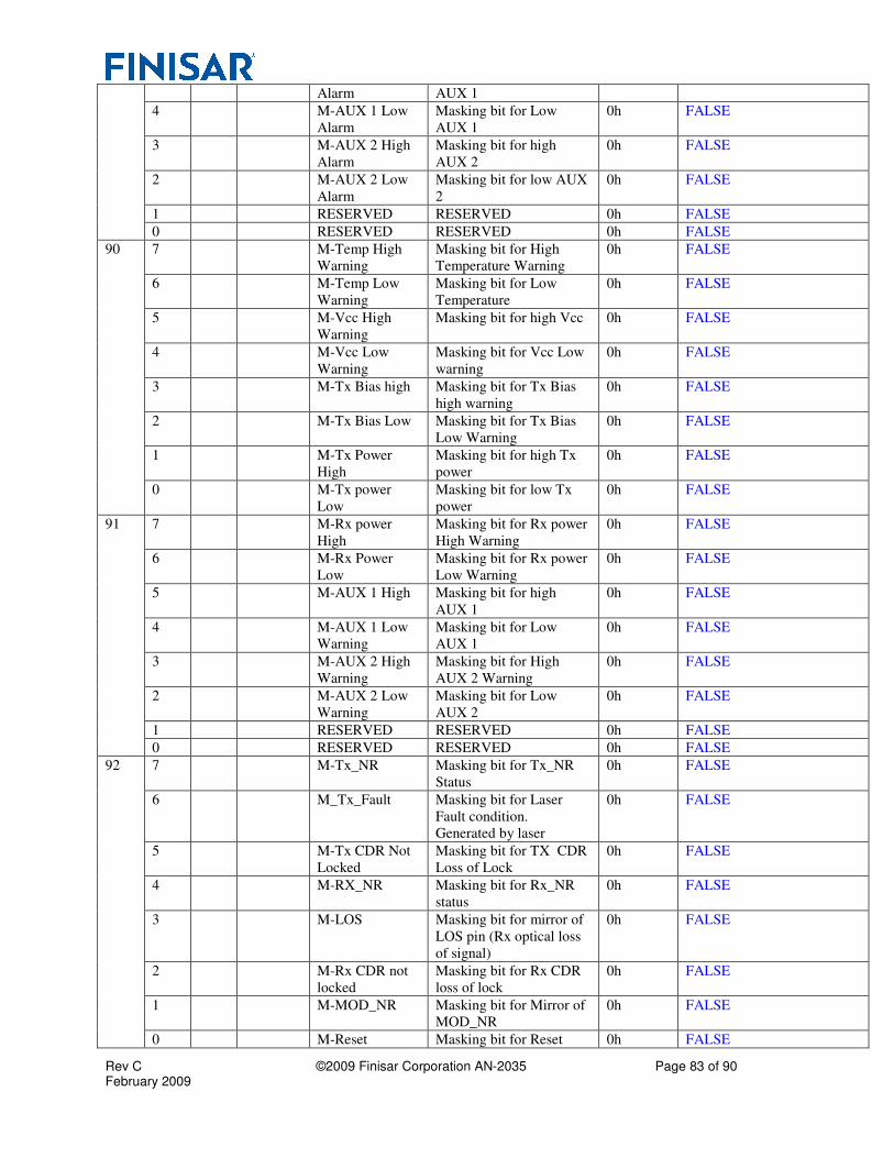
Rev C ©2009 Finisar Corporation AN-2035 Page 83 of 90 February 2009
Alarm AUX 1
4 M-AUX 1 Low
Alarm
Masking bit for Low
AUX 1
0h FALSE
3 M-AUX 2 High
Alarm
Masking bit for high
AUX 2
0h FALSE
2 M-AUX 2 Low
Alarm
Masking bit for low AUX
2
0h FALSE
1 RESERVED RESERVED 0h FALSE
0 RESERVED RESERVED 0h FALSE
90 7 M-Temp High
Warning
Masking bit for High
Temperature Warning
0h FALSE
6 M-Temp Low
Warning
Masking bit for Low
Temperature
0h FALSE
5 M-Vcc High
Warning
Masking bit for high Vcc 0h FALSE
4 M-Vcc Low
Warning
Masking bit for Vcc Low
warning
0h FALSE
3 M-Tx Bias high Masking bit for Tx Bias
high warning
0h FALSE
2 M-Tx Bias Low Masking bit for Tx Bias
Low Warning
0h FALSE
1 M-Tx Power
High
Masking bit for high Tx
power
0h FALSE
0 M-Tx power
Low
Masking bit for low Tx
power
0h FALSE
91 7 M-Rx power
High
Masking bit for Rx power
High Warning
0h FALSE
6 M-Rx Power
Low
Masking bit for Rx power
Low Warning
0h FALSE
5 M-AUX 1 High Masking bit for high
AUX 1
0h FALSE
4 M-AUX 1 Low
Warning
Masking bit for Low
AUX 1
0h FALSE
3 M-AUX 2 High
Warning
Masking bit for High
AUX 2 Warning
0h FALSE
2 M-AUX 2 Low
Warning
Masking bit for Low
AUX 2
0h FALSE
1 RESERVED RESERVED 0h FALSE
0 RESERVED RESERVED 0h FALSE
92 7 M-Tx_NR Masking bit for Tx_NR
Status
0h FALSE
6 M_Tx_Fault Masking bit for Laser
Fault condition.
Generated by laser
0h FALSE
5 M-Tx CDR Not
Locked
Masking bit for TX CDR
Loss of Lock
0h FALSE
4 M-RX_NR Masking bit for Rx_NR
status
0h FALSE
3 M-LOS Masking bit for mirror of
LOS pin (Rx optical loss
of signal)
0h FALSE
2 M-Rx CDR not
locked
Masking bit for Rx CDR
loss of lock
0h FALSE
1 M-MOD_NR Masking bit for Mirror of
MOD_NR
0h FALSE
0 M-Reset Masking bit for Reset 0h FALSE
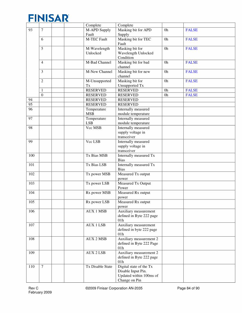
Rev C ©2009 Finisar Corporation AN-2035 Page 84 of 90 February 2009
Complete Complete
93 7 M-APD Supply
Fault
Masking bit for APD
Supply
0h FALSE
6 M-TEC Fault Masking bit for TEC
Fault
0h FALSE
5 M-Wavelength
Unlocked
Masking bit for
Wavelength Unlocked
Condition
0h FALSE
4 M-Bad Channel Masking bit for bad
channel
0h FALSE
3 M-New Channel Masking bit for new
channel
0h FALSE
2 M-Unsupported
Tx
Masking bit for
Unsupported Tx
0h FALSE
1 RESERVED RESERVED 0h FALSE
0 RESERVED RESERVED 0h FALSE
94 RESERVED RESERVED
95 RESERVED RESERVED
96 Temperature
MSB
Internally measured
module temperature
97 Temperature
LSB
Internally measured
module temperature
98 Vcc MSB Internally measured
supply voltage in
transceiver
99 Vcc LSB Internally measured
supply voltage in
transceiver
100 Tx Bias MSB Internally measured Tx
Bias
101 Tx Bias LSB Internally measured Tx
Bias
102 Tx power MSB Measured Tx output
power
103 Tx power LSB Measured Tx Output
Power
104 Rx power MSB Measured Rx output
power
105 Rx power LSB Measured Rx output
power
106 AUX 1 MSB Auxiliary measurement
defined in Byte 222 page
01h
107 AUX 1 LSB Auxiliary measurement
defined in byte 222 page
01h
108 AUX 2 MSB Auxiliary measurement 2
defined in Byte 222 Page
01h
109 AUX 2 LSB Auxiliary measurement 2
defined in Byte 222 page
01h
110 7 Tx Disable State Digital state of the Tx
Disable Input Pin.
Updated within 100ms of
Change on Pin
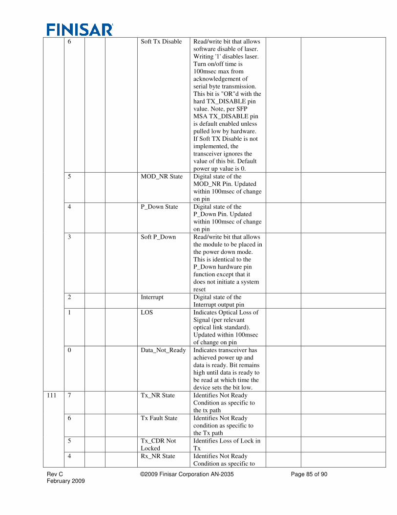
Rev C ©2009 Finisar Corporation AN-2035 Page 85 of 90 February 2009
6 Soft Tx Disable Read/write bit that allows
software disable of laser.
Writing '1' disables laser.
Turn on/off time is
100msec max from
acknowledgement of
serial byte transmission.
This bit is "OR"d with the
hard TX_DISABLE pin
value. Note, per SFP
MSA TX_DISABLE pin
is default enabled unless
pulled low by hardware.
If Soft TX Disable is not
implemented, the
transceiver ignores the
value of this bit. Default
power up value is 0.
5 MOD_NR State Digital state of the
MOD_NR Pin. Updated
within 100msec of change
on pin
4 P_Down State Digital state of the
P_Down Pin. Updated
within 100msec of change
on pin
3 Soft P_Down Read/write bit that allows
the module to be placed in
the power down mode.
This is identical to the
P_Down hardware pin
function except that it
does not initiate a system
reset
2 Interrupt Digital state of the
Interrupt output pin
1 LOS Indicates Optical Loss of
Signal (per relevant
optical link standard).
Updated within 100msec
of change on pin
0 Data_Not_Ready Indicates transceiver has
achieved power up and
data is ready. Bit remains
high until data is ready to
be read at which time the
device sets the bit low.
111 7 Tx_NR State Identifies Not Ready
Condition as specific to
the tx path
6 Tx Fault State Identifies Not Ready
condition as specific to
the Tx path
5 Tx_CDR Not
Locked
Identifies Loss of Lock in
Tx
4 Rx_NR State Identifies Not Ready
Condition as specific to
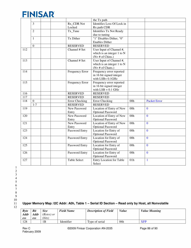
Rev C ©2009 Finisar Corporation AN-2035 Page 86 of 90 February 2009
the Tx path
3 Rx_CDR Not
Locked
Identifies Loss Of Lock in
Rx path CDR
2 Tx_Tune Identifies Tx Not Ready
due to tuning
1 Tx Dither "1" Disables Dither, "0"
Enables Dither
0 RESERVED RESERVED
112 Channel # Set User Input of Channel #,
which is an integer 1 to N
(N= # of Chins.)
113 Channel # Set User Input of Channel #,
which is an integer 1 to N
(N= # of Chans.)
114 Frequency Error Frequency error reported
in 16 bit signed integer
with LSB= 0.1GHz
115 Frequency Error Frequency error reported
in 16 bit signed integer
with LSB = 0.1 GHz
116 RESERVED RESERVED
117 RESERVED RESERVED
118 0 Error Checking Error Checking 00h Packet Error
1-7 RESERVED RESERVED
119 New Password
Entry
Location of Entry of New
Optional Password
00h 0
120 New Password
Entry
Location of Entry of New
Optional Password
00h 0
121 New Password
Entry
Location of Entry of New
Optional Password
00h 0
123 Password Entry Location for Entry of
Optional Password
00h 0
124 Password Entry Location for Entry of
Optional Password
00h 0
125 Password Entry Location for Entry of
Optional Password
00h 0
126 Password Entry Location for Entry of
Optional Password
00h 0
127 Table Select Entry Location for Table
Select
01h 1
1
2
3
4
5
6
7
8
9
10
Upper Memory Map: I2C Addr: A0h, Table 1 – Serial ID Section – Read only by Host, all Nonvolatile 11
12
Byte
Addr
ess
Bit
Addr
ess
Size
(Bytes) or
(bits)
Field Name Description of Field Value Value Meaning
128 1B Identifier Type of serial 06h XFP
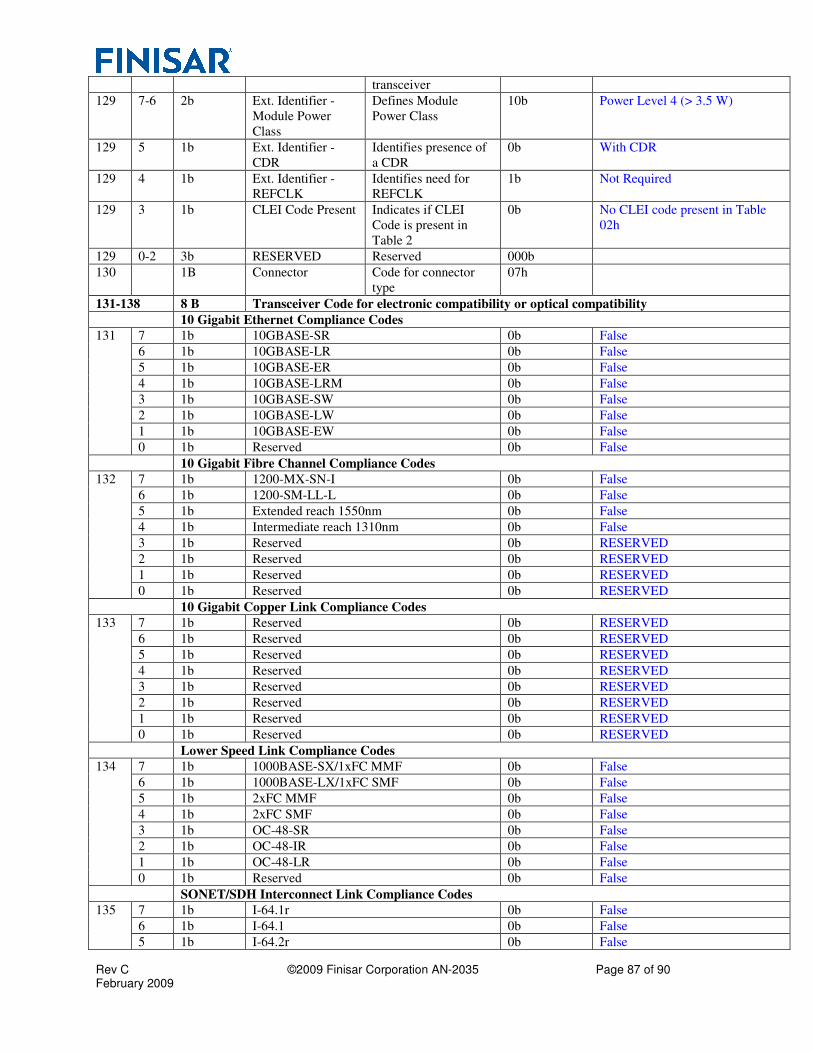
Rev C ©2009 Finisar Corporation AN-2035 Page 87 of 90 February 2009
transceiver
129 7-6 2b Ext. Identifier -
Module Power
Class
Defines Module
Power Class
10b Power Level 4 (> 3.5 W)
129 5 1b Ext. Identifier -
CDR
Identifies presence of
a CDR
0b With CDR
129 4 1b Ext. Identifier -
REFCLK
Identifies need for
REFCLK
1b Not Required
129 3 1b CLEI Code Present Indicates if CLEI
Code is present in
Table 2
0b No CLEI code present in Table
02h
129 0-2 3b RESERVED Reserved 000b
130 1B Connector Code for connector
type
07h
131-138 8 B Transceiver Code for electronic compatibility or optical compatibility
10 Gigabit Ethernet Compliance Codes
131 7 1b 10GBASE-SR 0b False
6 1b 10GBASE-LR 0b False
5 1b 10GBASE-ER 0b False
4 1b 10GBASE-LRM 0b False
3 1b 10GBASE-SW 0b False
2 1b 10GBASE-LW 0b False
1 1b 10GBASE-EW 0b False
0 1b Reserved 0b False
10 Gigabit Fibre Channel Compliance Codes
132 7 1b 1200-MX-SN-I 0b False
6 1b 1200-SM-LL-L 0b False
5 1b Extended reach 1550nm 0b False
4 1b Intermediate reach 1310nm 0b False
3 1b Reserved 0b RESERVED
2 1b Reserved 0b RESERVED
1 1b Reserved 0b RESERVED
0 1b Reserved 0b RESERVED
10 Gigabit Copper Link Compliance Codes
133 7 1b Reserved 0b RESERVED
6 1b Reserved 0b RESERVED
5 1b Reserved 0b RESERVED
4 1b Reserved 0b RESERVED
3 1b Reserved 0b RESERVED
2 1b Reserved 0b RESERVED
1 1b Reserved 0b RESERVED
0 1b Reserved 0b RESERVED
Lower Speed Link Compliance Codes
134 7 1b 1000BASE-SX/1xFC MMF 0b False
6 1b 1000BASE-LX/1xFC SMF 0b False
5 1b 2xFC MMF 0b False
4 1b 2xFC SMF 0b False
3 1b OC-48-SR 0b False
2 1b OC-48-IR 0b False
1 1b OC-48-LR 0b False
0 1b Reserved 0b False
SONET/SDH Interconnect Link Compliance Codes
135 7 1b I-64.1r 0b False
6 1b I-64.1 0b False
5 1b I-64.2r 0b False
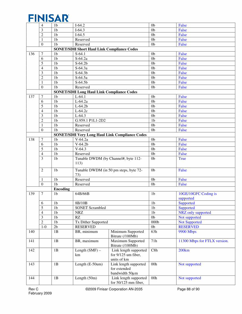
Rev C ©2009 Finisar Corporation AN-2035 Page 88 of 90 February 2009
4 1b I-64.2 0b False
3 1b I-64.3 0b False
2 1b I-64.5 0b False
1 1b Reserved 0b False
0 1b Reserved 0b False
SONET/SDH Short Haul Link Compliance Codes
136 7 1b S-64.1 0b False
6 1b S-64.2a 0b False
5 1b S-64.2b 0b False
4 1b S-64.3a 0b False
3 1b S-64.3b 0b False
2 1b S-64.5a 0b False
1 1b S-64.5b 0b False
0 1b Reserved 0b False
SONET/SDH Long Haul Link Compliance Codes
137 7 1b L-64.1 0b False
6 1b L-64.2a 0b False
5 1b L-64.2b 0b False
4 1b L-64.2c 0b False
3 1b L-64.3 0b False
2 1b G.959.1 P1L1-2D2 1b False
1 1b Reserved 0b False
0 1b Reserved 0b False
SONET/SDH Very Long Haul Link Compliance Codes
138 7 1b V-64.2a 0b False
6 1b V-64.2b 0b False
5 1b V-64.3 0b False
4 1b Reserved 0b False
3 1b Tunable DWDM (by Channel#, byte 112-
113)
0b True
2 1b Tunable DWDM (in 50 pm steps, byte 72-
73)
0b False
1 1b Reserved 0b False
0 1b Reserved 0b False
Encoding
139 7 1b 64B/66B 1b 10GE/10GFC Coding is
supported
6 1b 8B/10B 1b Supported
5 1b SONET Scrambled 1b Supported
4 1b NRZ 1b NRZ only supported
3 1b RZ 0b Not supported
2 1b Tx Dither Supported 000b Not Supported
1-0 2b RESERVED 0b RESERVED
140 1B BR, minimum Minimum Supported
Bitrate (/100Mb)
63h 9900 Mbps
141 1B BR, maximum Maximum Supported
Bitrate (/100Mb)
71h 11300 Mbps for FTLX version.
142 1B Length (SMF) –
km
Link length supported
for 9/125 um fiber,
units of km
C8h 200km
143 1B Length (E-50um) Link length supported
for extended
bandwidth 50µm
00h Not supported
144 1B Length (50m) Link length supported
for 50/125 mm fiber,
00h Not supported
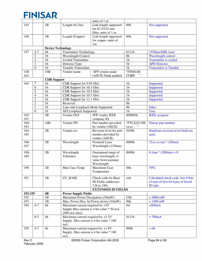
Rev C ©2009 Finisar Corporation AN-2035 Page 89 of 90 February 2009
units of 1 m
145 1B Length (62.5m) Link length supported
for 62.5/125 mm
fiber, units of 1 m
00h Not supported
146 1B Length (Copper) Link length supported
for copper, units of
1m
00h Not supported
Device Technology
147 4-7 4b Transmitter Technology 0111b 1550nm EML laser
3 1b Wavelength Control 0b Wavelength control
2 1b Cooled Transmitter 1b Transmitter is cooled
1 1b Detector Type 1b APD Detector
0 1b Tunable Transmitter 1b Transmitter is Tunable
148-
163
16B Vendor name SFP vendor name
(ASCII) blank padded
“FINISAR
CORP. ”
CDR Support
164 7 1b CDR Support for 9.95 Gb/s 1b Supported
6 1b CDR Support for 10.3 Gb/s 1b Supported
5 1b CDR Support for 10.5 Gb/s 1b Supported
4 1b CDR Support for 10.7 Gb/s 1b Supported
3 1b CDR Support for 11.1 Gb/s 1b Supported
2 1b Reserved 0b
1 1b Line-side Loopback Mode Supported 0b False
0 1b XFI Loopback Supported 1b True
165-
167
3B Vendor OUI SFP vendor IEEE
company ID
009065h IEEE assigned
168-
183
16B Vendor PN Part number provided
by vendor (ASCII)
“FTLX4213M
xxxx ”
Finisar part number
184-
185
2B Vendor rev Revision level for part
number provided by
vendor (ASCII)
3030h Hardware revision level field not
used
186-
187
2B Wavelength Nominal Laser
Wavelength (1/20nm)
0000h 15xx.xx nm * (20/nm)
188-
189
2B Wavelength
Tolerance
Guaranteed range of
laser wavelength +/-
value from nominal
Wavelength
0008h 0.1nm * (200/nm) = 8
190 1B Max Case Temp Maximum Case
Temperature
46h 70ºC
191 1B CC_BASE Check code for Base
ID Fields (addresses
128 to 190)
xxh Calculated check code, low 8 bits
of sum of first 64 bytes of Serial
ID info.
EXTENDED ID FIELDS
192-195 4B Power Supply Fields
192 1B Maximum Power Dissipation (/20mW) C8h = 4000 mW
193 1B Max. Power Diss. In Power-down (/10mW) 96h = 1500 mW
194 4-7 4b Maximum current required by +5V
Supply.Max current is 4 bit value * 50 mA.
[500 mA max]
0A =500mA
0-3 4b Maximum current required by +3.3V
Supply. Max current is 4 bit value * 100
mA.
0111b = 700mA
195 4-7 4b Maximum current required by +1.8V
Supply. Max current is 4 bit value * 100
mA.
000b = 00
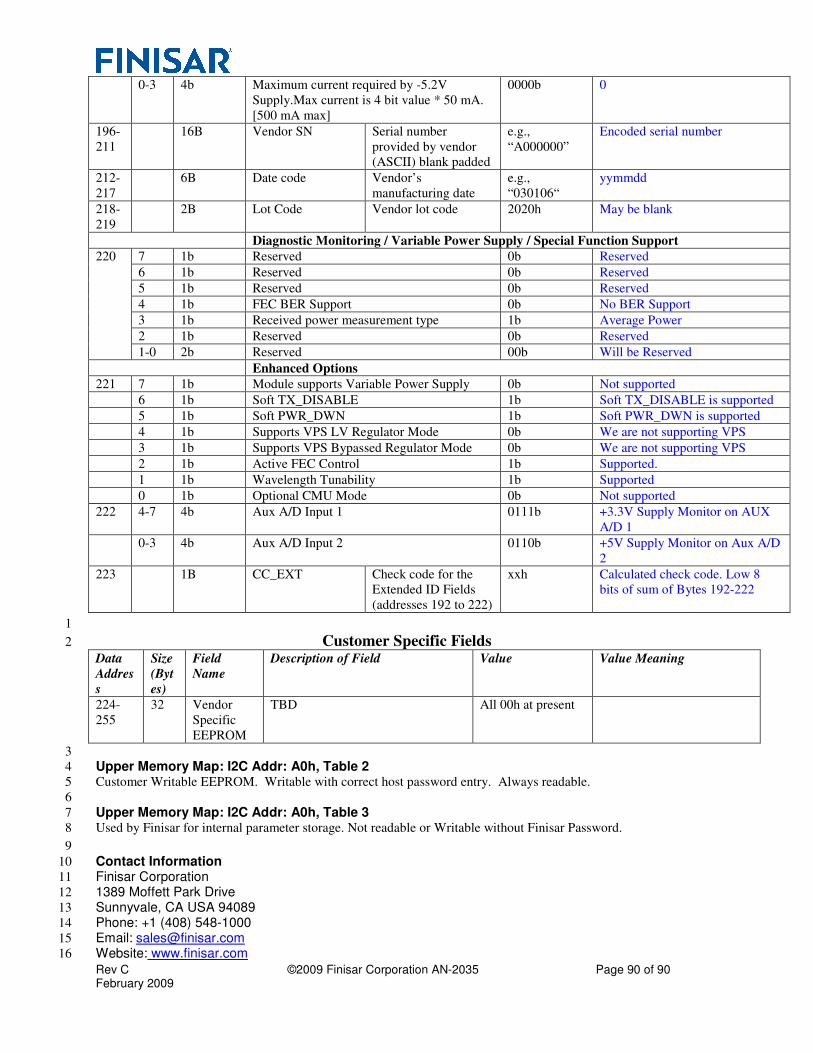
Rev C ©2009 Finisar Corporation AN-2035 Page 90 of 90 February 2009
0-3 4b Maximum current required by -5.2V
Supply.Max current is 4 bit value * 50 mA.
[500 mA max]
0000b 0
196-
211
16B Vendor SN Serial number
provided by vendor
(ASCII) blank padded
e.g.,
“A000000”
Encoded serial number
212-
217
6B Date code Vendor’s
manufacturing date
e.g.,
“030106“
yymmdd
218-
219
2B Lot Code Vendor lot code 2020h May be blank
Diagnostic Monitoring / Variable Power Supply / Special Function Support
220 7 1b Reserved 0b Reserved
6 1b Reserved 0b Reserved
5 1b Reserved 0b Reserved
4 1b FEC BER Support 0b No BER Support
3 1b Received power measurement type 1b Average Power
2 1b Reserved 0b Reserved
1-0 2b Reserved 00b Will be Reserved
Enhanced Options
221 7 1b Module supports Variable Power Supply 0b Not supported
6 1b Soft TX_DISABLE 1b Soft TX_DISABLE is supported
5 1b Soft PWR_DWN 1b Soft PWR_DWN is supported
4 1b Supports VPS LV Regulator Mode 0b We are not supporting VPS
3 1b Supports VPS Bypassed Regulator Mode 0b We are not supporting VPS
2 1b Active FEC Control 1b Supported.
1 1b Wavelength Tunability 1b Supported
0 1b Optional CMU Mode 0b Not supported
222 4-7 4b Aux A/D Input 1 0111b +3.3V Supply Monitor on AUX
A/D 1
0-3 4b Aux A/D Input 2 0110b +5V Supply Monitor on Aux A/D
2
223 1B CC_EXT Check code for the
Extended ID Fields
(addresses 192 to 222)
xxh Calculated check code. Low 8
bits of sum of Bytes 192-222
1
Customer Specific Fields 2
Data
Addres
s
Size
(Byt
es)
Field
Name
Description of Field Value Value Meaning
224-
255
32 Vendor
Specific
EEPROM
TBD All 00h at present
3
Upper Memory Map: I2C Addr: A0h, Table 2 4
Customer Writable EEPROM. Writable with correct host password entry. Always readable. 5
6
Upper Memory Map: I2C Addr: A0h, Table 3 7
Used by Finisar for internal parameter storage. Not readable or Writable without Finisar Password. 8
9
Contact Information 10
Finisar Corporation 11
1389 Moffett Park Drive 12
Sunnyvale, CA USA 94089 13
Phone: +1 (408) 548-1000 14
Email: [email protected] 15
Website: www.finisar.com 16