Embed Size (px)
DESCRIPTION
http://www.ij-ms.org/paperInfo.aspx?ID=9097 Molybdenum oxide (MoO3) films were deposited on glass and silicon substrates by sputtering of molybdenum target at different substrate temperatures in the range 473-573 K at a constant oxygen partial pressure of 4x10⁻⁴ mbar employing RF magnetron sputtering technique. The effect of substrate temperature on structural, morphological, electrical and optical properties of the MoO3 films was systematically studied. X-ray diffraction studies revealed that the films formed at 303 K were amorphous in nature, while those deposited at substrate temperature 473 K were orthorhombic MoO3 with crystallite size of 27 nm and the crystallinity increased with increase of substrate temperature. The scanning electron micrographs of the films deposited at 303 K were of fine grain structure in amorphous back ground and the films formed at 523 K contained the grains with shape of platelets piled one over the other with size of about 1 μm. Fourier transform
Citation preview
www.ij-ms.org International Journal of Material Science (IJMSCI) Volume 4 Issue 2, June 2014 doi: 10.14355/ijmsci.2014.0402.06
Substrate Temperature Influenced Physical and Electrochromic Properties of MoO3 Thin Films S. Subbarayudu*, V. Madhavi, S. Uthanna
Department of Physics, Sri Venkateswara University, Tirupati - 517 502, India *[email protected]; [email protected]; [email protected]
Received 24 June, 2013; Revised 4 February, 2014; Accepted 3 March, 2014; Published 20 June, 2014 © 2014 Science and Engineering Publishing Company Abstract :
Molybdenum oxide (MoO3) films were deposited on glass and silicon substrates by sputtering of molybdenum target at different substrate temperatures in the range 473-573 K at a constant oxygen partial pressure of 4x10⁻⁴ mbar employing RF magnetron sputtering technique. The effect of substrate temperature on structural, morphological, electrical and optical properties of the MoO3 films was systematically studied. X-ray diffraction studies revealed that the films formed at 303 K were amorphous in nature, while those deposited at substrate temperature 473 K were orthorhombic MoO3 with crystallite size of 27 nm and the crystallinity increased with increase of substrate temperature. The scanning electron micrographs of the films deposited at 303 K were of fine grain structure in amorphous back ground and the films formed at 523 K contained the grains with shape of platelets piled one over the other with size of about 1 μm. Fourier transform infrared transmittance spectra exhibited the characteristic vibration modes of MoO3. The electrical resistivity of the films decreased with increase of substrate temperature due to partial filling of oxygen ion vacancies. The optical band gap and refractive index of the films increased with the increase of substrate temperature. The MoO3 films formed at substrate temperature of 523 K exhibits high optical modulation of 22% and coloration efficiency of 30 cm2/C.
Keywords
Molybdenum Oxide Films; RF Magnetron Sputtering; Substrate Temperature; Structural; Electrochromic Properties
Introduction
Transition metal oxides are semiconductors and have many technological applications in different fields such as lithium secondary batteries, display devices, optical smart windows, low cost electrochromic devices and gas sensors [Granqvist 1995, Julien 1994].
Molybdenum oxide (MoO3), one among the transition metal oxides, exhibits interesting structural, chemical and optical properties. An orthorhombic α- phase MoO3 layered structure is potential for lithium batteries and optical smart windows [Li et al. 2006]. Molybdenum oxide is good electrochromic material since it has oxygen deficient perovskite structure (α- and β- phases) which is suitable for intercalation and de-intercalation due to polyvalent oxidation states, which leads to bluish coloration. It also exhibits photo- and gasochromic (coloration) effects by virtue of which the material is of potential for the development of electronic display devices [Patil et al. 2008, Prasad et al. 2003, Scarminio et al. 1997]. Nanocrystalline MoO3 films also find applications in nanodevices and nanosensors [Patzke et al. 2004, Taurino et al. 2006]. It is a promising candidate for a back contact layer for cadmium telluride solar cells in superstrate configuration due to its high work function, which reduces the contact barrier [Gretener et al. 2013]. Various physical thin film deposition techniques such as electron beam evaporation [Sabhapathi et al. 1995, Sivakumar et al. 2007], pulsed laser deposition [Ramana et al. 2007, Ramana et al. 2006], thermal evaporation [Sain et al. 2005 Yang et al. 2009] and sputtering [Okumu et al. 2006, Mahamed et al . 2007, Uthanna et al. 2010, Srinivasa Rao et al. 2009, Navas et al. 2009], and chemical methods such as spray pyrolysis [Boudaoud et al. 2006, Martinez et al. 2013], electrodeposition [Patil et al. 2006], sol-gel process [Dhanasankar et al. 2011, Fan et al. 2011] and chemical vapor deposition [Itoh et al. 2008] were used for the growth of MoO3 films. Magnetron sputter deposition is an industrially practiced technique for deposition of oxide films. The physical properties of the sputter
78
International Journal of Material Science (IJMSCI) Volume 4 Issue 2, June 2014 www.ij-ms.org
deposited MoO3 films depend critically on the sputter parameters such as oxygen partial pressure, substrate temperature, sputter power, sputter pressure and post-deposition heat treatment. In our earlier investigation, α-phase MoO3 films were grown by thermal oxidation of DC magnetron sputtered metallic molybdenum films and their electrochemical and electrochromic properties were studied[Madhavi et al. 2013]. In the present investigation, thin films of MoO3 were formed by RF magnetron sputtering technique at different of substrate temperatures and study their structure, surface morphology, electrical and optical properties. The electrochromic response of the MOO3
films was studied and reported.
Experimental
Preparation And Characterization Of Moo3 Thin Films
MoO3 thin films were deposited onto glass and silicon substrates held at different temperatures in the range 303-573 K by sputtering of pure metallic molybdenum target in oxygen and argon gas mixture using reactive RF magnetron sputtering technique. Metallic molybdenum target (99.999% pure) with 50 mm diameter and 3 mm thickness was used for sputtering. The sputter chamber was evacuated by employing diffusion pump and rotary pump combination to achieve base pressure of 4x10⁻⁶ mbar. Pressure in the sputter chamber was measured with digital Pirani – Penning gauges. After achieving base pressure of 4x10-
6 mbar, oxygen gas was admitted in to the sputter chamber to the pressures in the range from 8x10⁻⁵ mbar to 8x10⁻⁴ mbar. Later, argon gas was admitted to the sputter pressure of 4x 10⁻² mbar. The required quantities of oxygen and argon gases were admitted into the sputter chamber through fine controlled needle valves followed by Aalborg mass flow controllers (Model GFC 17). RF power of 150 W was supplied to the sputter target using RF power generator (Advance Energy Model ATX-600 W) for deposition of MoO3 films. The sputter parameters fixed during the growth of the MoO3 films are given in table 1.
The deposited MoO3 films were characterized by studying their chemical composition, crystallographic structure and surface morphology, chemical binding configuration, electrical and optical properties. The thickness of the deposited films was measured with a mechanical Veeco Dektak (Model 150) depth profilometer. The chemical composition of the films
was analysed with energy dispersive X-ray Analysis (Oxford instruments Inca Penta FETx3) attached to a scanning electron microscope (Carl Zeiss, model EVO MA15). The crystallographic structure of the films was determined by using X-ray diffractometer (Bruker D8 Advance Diffractometer) with copper Kα radiation with wavelength of λ = 0.15406 nm. The X-ray diffraction profiles were taken for a 2θ range between 10 and 600 in steps of 0.050. The surface morphology of the films was analysed with scanning electron microscope (Hitachi SEM Model S-400). The chemical binding configuration of the films formed on silicon substrates was analyzed with Fourier transform infrared spectrophotometer (Nicolet Magana IR 750) and recorded the optical transmittance in the wavenumber range 400–1500 cm-1. The electrical resistivity of the films was measured with four point probe method. The optical transmittance of the films formed on glass substrates was recorded using UV-Vis-NIR double beam spectrophotometer (Perkin - Elmer Spectrophotometer Lambda 950) in the wavelength range 300 - 1500 nm.
TABLE 1. SPUTTER PARAMETERS FIXED DURING THE GROWTH OF MOO3 FILMS
------------------------------------------------------------------------- Sputter target : Molybdenum Target to substrate distance : 65 mm Base pressure : 4x10⁻⁶ mbar Oxygen partial pressure (pO2) : 8x10⁻⁴ - 8x10⁻⁴ mbar Substrate temperature (Ts) : 303 - 573 K Sputtering pressure : 4x10⁻² mbar Sputter power : 150 W Deposition time : 120 min ________________________________________________
Results And Discussion
In oder to optimise the oxygen partial pressure for the growth of the films, the MoO3 films were deposited at different oxygen partial pressures in the range 8x10⁻⁴ - 8x10⁻⁴ mbar. The chemical composition of the deposited films was determined by using EDAX. Figure 1 shows the representative energy dispersive X-ray analysis spectrum of the film formed a oxygen partial pressure of 4x10⁻⁴ mbar. The spectrum contained the characteristic constituent of molybdenum and oxygen in the films. The chemical constituents present in the films formed at different oxygen partial pressures are shown in table 2.
It is seen from the table that the films formed at low oxygen partial partial pressure of 8x10⁻⁵ mbar contained less quantity of oxygen than the required to form compound of MoO3. As the oxygen partial
79

www.ij-ms.org International Journal of Material Science (IJMSCI) Volume 4 Issue 2, June 2014
pressure increased to 4x10⁻⁴ mbar the films exhibited the atomic ratio of 3.02 : 1. It revealed that the oxygen partial pressure of 4x10⁻⁴ mbar is an optimum to produce nearly stiochiometric MoO3 films. Hence an oxygen partial pressure of 4x10⁻⁴ mbar was fixed to form the films at different substrate temperatures in order to investigate their physical properties.
FIG. 1 EDAX SPECTRUM OF MoO3 FILM FORMED AT OXYGEN
PARTIAL PRESSURE OF 4X10⁻⁴ mbar
TABLE 2 CHEMICAL COMPOSITION OF MOO3 FILMS FORMED AT DIFFERENT OXYGEN OARTIAL PRESSURES
------------------------------------------------------------------------- pO2 (mbar) Mo (at %) O (at %) Mo / O ------------------------------------------------------------------------- 8x10⁻⁵ 79.2 20.8 3.80 2x10⁻⁴ 76.4 23.6 3.23 4x10⁻⁴ 75.2 24.8 3.03
Deposition Rate
Substrate temperature has significant influence on the thickness of the deposited MoO3 films. The thickness of the deposited films was in the range 1.94 - 2.29 μm. Figure 2 shows the dependence of deposition rate on the substrate temperature of the MoO3 films.
The deposition rate of the films formed at room temperature (303 K) was 16.2 nm/min. As the substrate temperature increased from 473 K to 523 K, the deposition rate increased from 18.5 nm/min to 19.1 nm/min respectively. Due to the films formed at higher substrate temperature of 573 K, there was a slight decrease in the deposition rate to 18.3 nm/min. It is noted that the formation of oxide phase during reactive sputtering occurs almost nearly substrate surface where the rate of reaction increases with increase of substrate temperature, hence leading to the higher deposition rate. Further increase of substrate temperature to 573 K resulted in a slight decrease in the deposition rate to 16 nm/min. The decrease of deposition rate at higher substrate temperatures may
be due to the balance between the number of sputtered species arriving on the substrate surface and the species leaving from the substrate surface due to the re-evaporation of the deposited film hence decrease in the deposition rate.
300 350 400 450 500 550 60010
15
20
25
Depo
sitio
n ra
te (n
m/m
in)
Substrate temperature (K)
pO2= 4x10⁻⁴ mbar
FIG. 2 VARIATION IN THE DEPOSITION RATE OF MoO3 FILMS
WITH SUBSTRATE TEMPERATURE
Structural Studies
Figure 3 shows the X-ray diffraction profiles of MoO3 films formed at different substrate temperatures. The films deposited at room temperature didn’t contain the characteristic diffraction reflections of MoO3, which revealed that the grown films were of X-ray amorphous. The films grown at substrate temperature of 473 K showed the diffraction peaks at 2θ = 12.80 and 26.30. These peaks were related to the (020) and (040) reflections of orthorhombic α- phase MoO3. The presence of (020) reflections revealed the growth of layer structured α- phase MoO3.
20 40 60
050
100150200
As deposited
0100200300400500
(040)
(020)
473 K
0
10000
20000
30000
(141)(02
1)
Intens
ity (C
ounts
/ sec)
523 K
2θ (Degrees)
0
10000
20000po2=4x10⁻⁴ mbar
Ts =573 K
FIG. 3 XRD PROFILES OF MoO3 FILMS DEPOSITED AT
DIFFERENT SUBSTRATE TEMPERATURES
80
International Journal of Material Science (IJMSCI) Volume 4 Issue 2, June 2014 www.ij-ms.org
The films formed at the substrate temperature of 523 K showed the diffraction peaks at 2θ = 12.90 related to the (020) reflection, 27.80 connected to (021) reflection and 43.20 for the (141) reflections of α- phase MoO3
[JCPDS Code No. 76 – 1003]. It is noted that the (040) reflection was disappeared at substrate temperature of 523 K. The intensity of diffraction peaks increased with increase of substrate temperature revealed the improvement in the crystallinity of the films. Due to the further increase of the substrate temperature to 573 K, the decrease in the intensity of diffraction peaks indicated the decrease in the crystallinity of the films. The decrease in the crystallinity at higher substrate temperature of 573 K may be due to the higher surface mobility of adatoms on the substrate which was thermally induced, hence the reduction in the crystallinity of the deposited MoO3 films. In the literature, Bouzidi et al. [2003] achieved α- phase MoO3 films by spray pyrolysis in the substrate temperatures range 523 - 573 K. Such a layered structured MoO3 films were achieved by Martinez et al. [2013] at substrate temperature range from 473 to 673 K by spray deposition. It is noted that Sivakumar et al. [2007] obtained α- phase MoO3 films at low substrate temperature of 473 K in electron beam evaporation. Yang et al. [2009] found that the mixed α- and β- phase MoO3 films in electron beam deposition. It was clearly indicated that the grown crystallographic structure of the MoO3 films mainly depends on the substrate temperature and the method of film growth.
The crystallite size (L) of the films was calculated from the X-ray diffraction peaks of (020) by using Debye - Scherrer’s relation [Cullity, 1974]
L = 0.89λ / β cosθ ------------- (1)
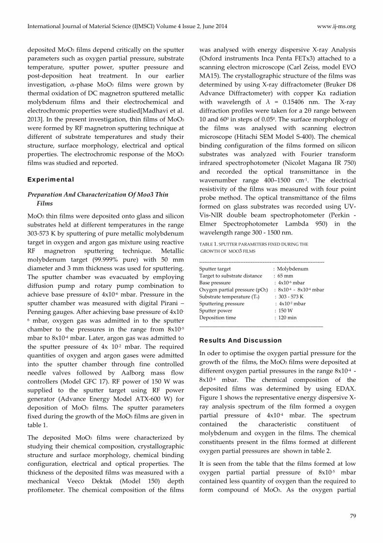
where λ is the wavelength of the X-rays (0.15406 nm), β the full width at half maximum of diffraction intensity measured in radians and θ the diffraction angle. Figure 4 shows the variation of crystallite size of MoO3 films with substrate temperature. The full width at half maximum of the peak (020) in the films decreased from 0.200 to 0.140 with increase of substrate temperature from 473 K to 523 K respectively. In terms of the further increase of substrate temperature to 573 K, it increased to 0.190. The crystallite size of the MoO3
films deposited at substrate temperature of 473 K was 27 nm. As the substrate temperature increased to 523 K, the crystallite size increased to 62 nm. At higher substrate temperature of 573 K, the crystallite size decreased to 43 nm. The crystallite size of the films
increased with increase of substrate temperature upto 523 K. At 523 K, the XRD shows that intensity of (0k0) reflection is maximum, indicating the layered structure of MoO3. On further increment of substrate temperature to 573 K the intensity of (0k0) reflection decreased and intensity of peaks (021) and (141) increased. It revealed that though the films at higher substrate temperature of 573 K were not of layer structured α- phase MoO3. At higher substrate temperature of 573 K, the crystallite size decreased to 43 nm due to the re-evaporation hence smaller size of crystallites was grown.
450 480 510 540 570 60020
40
60
80
pO2 = 4x10⁻⁴ mbar
Crys
talli
te si
ze (n
m)
Substrate temparature (K)
FIG. 4 VARIATION OF CRYSTALLITE SIZE OF MoO3 FILMS
WITH SUBSTRATE TEMPERATURE
In literature, Martinez et al. [2013] reported that the crystallite size decreased from 30 nm to 10 nm with increase of substrate temperature from 423 K to 553 K respectively in the MoO3 films formed by spray pyrolysis method. Fan et al. [2011] also noticed the decrease in the crystallite size from 32 nm to 25 nm with increase of substrate temperature from 573 K to 673 K in RF sputtered MoO3 films.
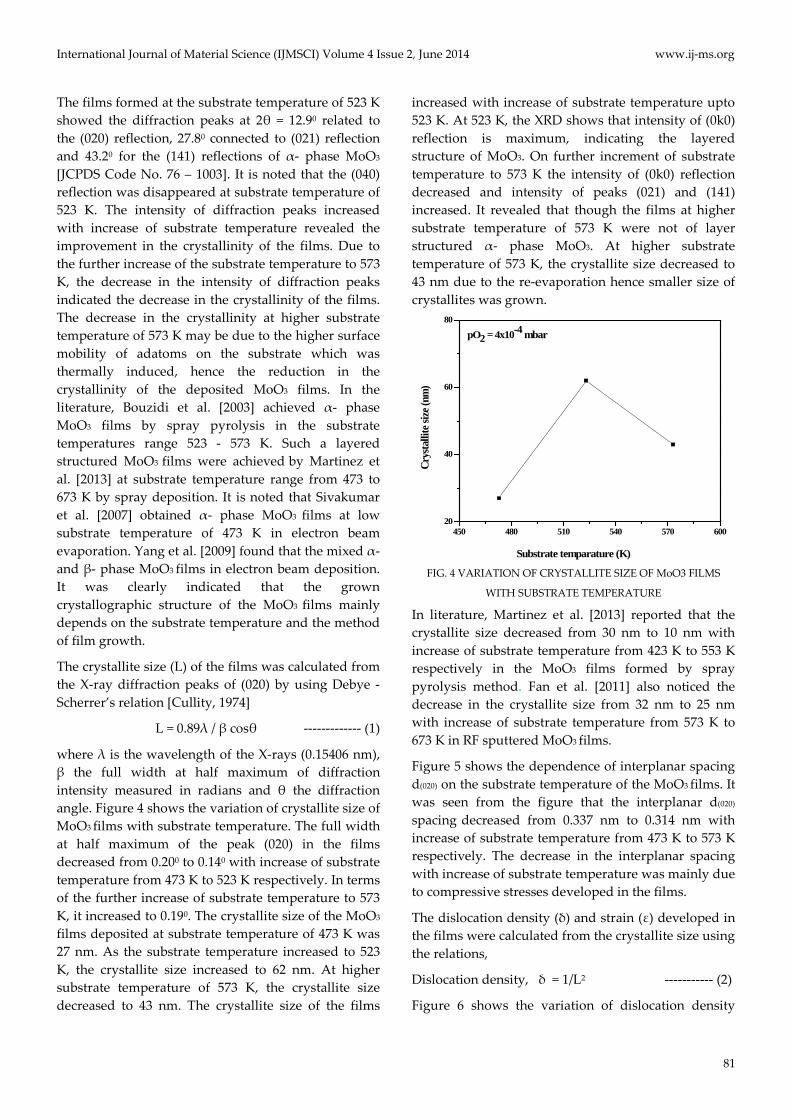
Figure 5 shows the dependence of interplanar spacing d(020) on the substrate temperature of the MoO3 films. It was seen from the figure that the interplanar d(020) spacing decreased from 0.337 nm to 0.314 nm with increase of substrate temperature from 473 K to 573 K respectively. The decrease in the interplanar spacing with increase of substrate temperature was mainly due to compressive stresses developed in the films.
The dislocation density (δ) and strain (ε) developed in the films were calculated from the crystallite size using the relations,
Dislocation density, δ = 1/L2 ----------- (2)
Figure 6 shows the variation of dislocation density
81
www.ij-ms.org International Journal of Material Science (IJMSCI) Volume 4 Issue 2, June 2014
developed in the MoO3 films with substrate temperature. The dislocation density of the films deposited at substrate temperature of 473 K was 1.4x10¹⁵ lines/m2 and it decreased to 2.6x10¹⁴ lines/m2 at substrate temperature of 523 K. On further increase of substrate temperature to 573 K, the dislocation density increased to 5.4x10¹⁴ lines/m2.
460 480 500 520 540 560 580
0.35
0.34
0.33
0.32
0.31
pO2= 4x10⁻⁴ mbar
Substrate temperature (K)
Inte
rpla
nar
spac
ing
d(0
20) (
nm)
0.3
FIG. 5 VARIATION IN THE INTER PLANAR d(020) SPACING OF
MoO3 FILMS WITH SUBSTRATE TEMPERATURE
460 480 500 520 540 560 580 600
pO2 = 4x10⁻⁴ mbar
Substrate temparature (K)
Dislo
catio
n de
nsity
(lin
e/m2 ) x
1014
0
5
10
15
FIG. 6 DEPENDENCE OF DISLOCATION DENSITY OF
MoO3 FILMS ON SUBSTRATE TEMPERATURE
The decrease in dislocation density in the films were mainly due to the enhancement in the crystallinity with increase of substrate temperature up to 523 K. At higher substrate temperature of 573 K there was a increase in the dislocation density and strain in the films.
Stress (σ) developed in the films was estimated from lattice parameter using the relation [Eckertova, 1984],
Stress, σ = Y[(a - ao) /2 ν ao ] ----------- (3)
where a is the experimentally determined lattice parameter, ao the bulk lattice parameter, ν the Poisson’s ratio and Y the Young’s modulus.
450 500 550 600-295
-290
-285
-280
-275
-270
Stre
ss (G
Pa)
Substrate temperature (K)
pO2 = 4x10⁻⁴ mbar
FIG. 7 VARIATION OF STRESS WITH SUBSTRATE
TEMPERATURE
Figure 7 shows the variation of stress in MoO3 with substrate temperature. It is seen from the figure that the stress in the films decresed from -273 to -290 GPa with increase of with increase of substrate temperature from 473 to 573 K respectively. The decrease of stress with increase of substrate temperature clearly indicated that the compressive stress decreased with the increase of substrate temperature.
Surface Morphology
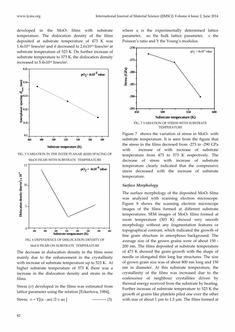
The surface morphology of the deposited MoO3 films was analyzed with scanning electron microscope. Figure 8 shows the scanning electron microscope images of the films formed at different substrate temperatures. SEM images of MoO3 films formed at room temperature (303 K) showed very smooth morphology without any fragmentation features or topographical contrast, which indicated the growth of fine grain structure in amorphous background. The average size of the grown grains were of about 150 - 200 nm. The films deposited at substrate temperature of 473 K showed the grain growth with the shape of needle or elongated thin long bar structures. The size of grown grain size was of about 800 nm long and 150 nm in diameter. At this substrate temperature, the crystallinity of the films was increased due to the coalescence of neighbour crystallites driven by thermal energy received from the substrate by heating. Further increase of substrate temperature to 523 K the growth of grains like platelets piled one over the other with size of about 1 μm to 1.5 μm. The films formed at
82
International Journal of Material Science (IJMSCI) Volume 4 Issue 2, June 2014 www.ij-ms.org
higher substrate of 573 K the size of the grains decreased to about 1.2 μm. In general, the MoO3 films grew with grains in the shape of needles platelets, elongated columns and rectangular shape depend on the deposition method employed and process parameters maintained during the deposition. Hence, the observed needle and platelet shaped grains achieved at higher substrate temperatures may be due to better mobility of adatoms or molecules to promote the growth. Yang et al. [ 2009] noticed the grains with pearl-like structure with platelets one over the other with size varied from 0.1 μm to 4 μm at substrate temperature of 373 K while at higher temperature of 673 K the average diameter of nanocrystallites of about 0.1 μm diameter and 3.5 μm long in electron beam evaporated MoO3 films. The grains with shape of platelets were also grown by Wu et al. [2009] in vapor transport deposited MoO3 films. Comini et al. [2008] achieved needle like nanoparticles with size about 200-400 nm at substrate temperature of 973 K in sol-gel deposited films.
FIG. 8 SEM IMAGES OF MoO3 FILMS FORMED AT DIFFERENT
SUBSTRATE TEMPERATURES: a) 303 K, b) 473 K, c) 523 K AND d) 573 K
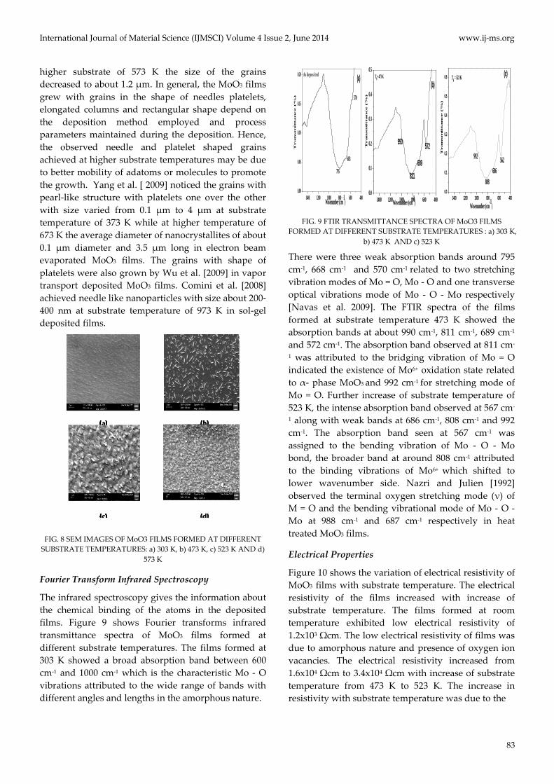
Fourier Transform Infrared Spectroscopy
The infrared spectroscopy gives the information about the chemical binding of the atoms in the deposited films. Figure 9 shows Fourier transforms infrared transmittance spectra of MoO3 films formed at different substrate temperatures. The films formed at 303 K showed a broad absorption band between 600 cm-1 and 1000 cm-1 which is the characteristic Mo - O vibrations attributed to the wide range of bands with different angles and lengths in the amorphous nature.
1400 1200 1000 800 600 4000.0
0.1
0.2
0.3
0.4
0.5
0.6 (c)
686562
808
992
Ts = 523 K
Wavenumber (cm-1)
Tran
sm
ittan
ce (
%)
1400 1200 1000 800 600 4000.0
0.1
0.2
0.3
0.4
0.5
(b)Ts= 473 K
Transm
ittance (
%)
Wavenumber (cm-1)
572
811689
990
1400 1200 1000 800 600 4000.00
0.05
0.10
0.15
0.20
Transm
ittance (
%)
Wavenumber (cm-1)
795
A s d e p o s i t e d (a)
570
683
FIG. 9 FTIR TRANSMITTANCE SPECTRA OF MoO3 FILMS
FORMED AT DIFFERENT SUBSTRATE TEMPERATURES : a) 303 K, b) 473 K AND c) 523 K
There were three weak absorption bands around 795 cm-1, 668 cm-1 and 570 cm-1 related to two stretching vibration modes of Mo = O, Mo - O and one transverse optical vibrations mode of Mo - O - Mo respectively [Navas et al. 2009]. The FTIR spectra of the films formed at substrate temperature 473 K showed the absorption bands at about 990 cm-1, 811 cm-1, 689 cm-1 and 572 cm-1. The absorption band observed at 811 cm-
1 was attributed to the bridging vibration of Mo = O indicated the existence of Mo6+ oxidation state related to α- phase MoO3 and 992 cm-1 for stretching mode of Mo = O. Further increase of substrate temperature of 523 K, the intense absorption band observed at 567 cm-
1 along with weak bands at 686 cm-1, 808 cm-1 and 992 cm-1. The absorption band seen at 567 cm-1 was assigned to the bending vibration of Mo - O - Mo bond, the broader band at around 808 cm-1 attributed to the binding vibrations of Mo6+ which shifted to lower wavenumber side. Nazri and Julien [1992] observed the terminal oxygen stretching mode (ν) of M = O and the bending vibrational mode of Mo - O - Mo at 988 cm-1 and 687 cm-1 respectively in heat treated MoO3 films.
Electrical Properties
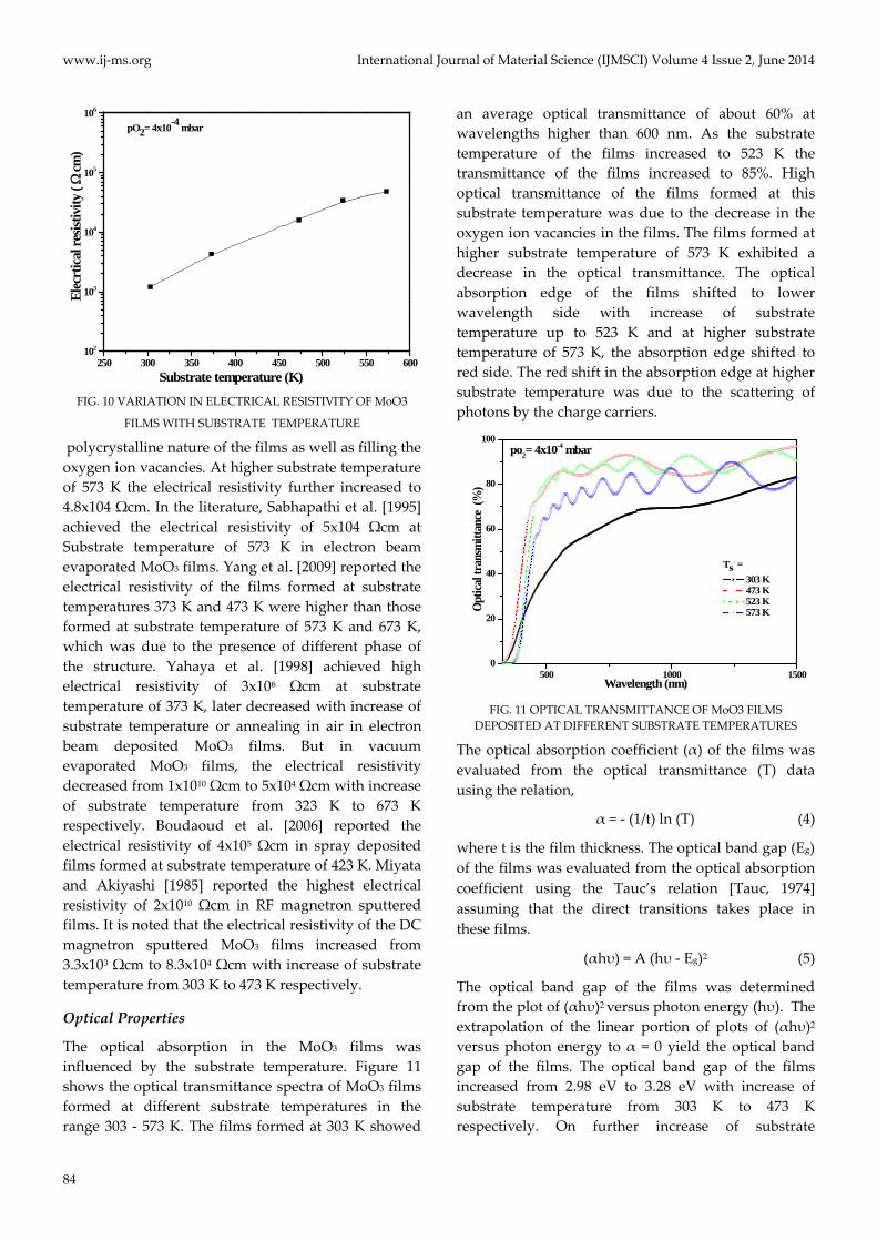
Figure 10 shows the variation of electrical resistivity of MoO3 films with substrate temperature. The electrical resistivity of the films increased with increase of substrate temperature. The films formed at room temperature exhibited low electrical resistivity of 1.2x10³ Ωcm. The low electrical resistivity of films was due to amorphous nature and presence of oxygen ion vacancies. The electrical resistivity increased from 1.6x10⁴ Ωcm to 3.4x10⁴ Ωcm with increase of substrate temperature from 473 K to 523 K. The increase in resistivity with substrate temperature was due to the
83
www.ij-ms.org International Journal of Material Science (IJMSCI) Volume 4 Issue 2, June 2014
250 300 350 400 450 500 550 600102
103
104
105
106
pO2= 4x10⁻⁴ mbar
Elec
rtica
l res
istiv
ity (
Ω cm
)
Substrate temperature (K)
FIG. 10 VARIATION IN ELECTRICAL RESISTIVITY OF MoO3
FILMS WITH SUBSTRATE TEMPERATURE
polycrystalline nature of the films as well as filling the oxygen ion vacancies. At higher substrate temperature of 573 K the electrical resistivity further increased to 4.8x10⁴ Ωcm. In the literature, Sabhapathi et al. [1995] achieved the electrical resistivity of 5x10⁴ Ωcm at Substrate temperature of 573 K in electron beam evaporated MoO3 films. Yang et al. [2009] reported the electrical resistivity of the films formed at substrate temperatures 373 K and 473 K were higher than those formed at substrate temperature of 573 K and 673 K, which was due to the presence of different phase of the structure. Yahaya et al. [1998] achieved high electrical resistivity of 3x10⁶ Ωcm at substrate temperature of 373 K, later decreased with increase of substrate temperature or annealing in air in electron beam deposited MoO3 films. But in vacuum evaporated MoO3 films, the electrical resistivity decreased from 1x10¹⁰ Ωcm to 5x10⁴ Ωcm with increase of substrate temperature from 323 K to 673 K respectively. Boudaoud et al. [2006] reported the electrical resistivity of 4x10⁵ Ωcm in spray deposited films formed at substrate temperature of 423 K. Miyata and Akiyashi [1985] reported the highest electrical resistivity of 2x10¹⁰ Ωcm in RF magnetron sputtered films. It is noted that the electrical resistivity of the DC magnetron sputtered MoO3 films increased from 3.3x10³ Ωcm to 8.3x10⁴ Ωcm with increase of substrate temperature from 303 K to 473 K respectively.
Optical Properties
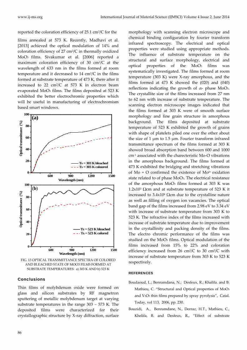
The optical absorption in the MoO3 films was influenced by the substrate temperature. Figure 11 shows the optical transmittance spectra of MoO3 films formed at different substrate temperatures in the range 303 - 573 K. The films formed at 303 K showed
an average optical transmittance of about 60% at wavelengths higher than 600 nm. As the substrate temperature of the films increased to 523 K the transmittance of the films increased to 85%. High optical transmittance of the films formed at this substrate temperature was due to the decrease in the oxygen ion vacancies in the films. The films formed at higher substrate temperature of 573 K exhibited a decrease in the optical transmittance. The optical absorption edge of the films shifted to lower wavelength side with increase of substrate temperature up to 523 K and at higher substrate temperature of 573 K, the absorption edge shifted to red side. The red shift in the absorption edge at higher substrate temperature was due to the scattering of photons by the charge carriers.
500 1000 15000
20
40
60
80
100po2= 4x10⁻⁴ mbar
Opt
ical t
rans
mitt
ance
(%
)
Wavelength (nm)
Ts = 303 K 473 K 523 K 573 K
FIG. 11 OPTICAL TRANSMITTANCE OF MoO3 FILMS
DEPOSITED AT DIFFERENT SUBSTRATE TEMPERATURES
The optical absorption coefficient (α) of the films was evaluated from the optical transmittance (T) data using the relation,
α = - (1/t) ln (T) (4)
where t is the film thickness. The optical band gap (Eg) of the films was evaluated from the optical absorption coefficient using the Tauc’s relation [Tauc, 1974] assuming that the direct transitions takes place in these films.
(αhυ) = A (hυ - Eg)2 (5)
The optical band gap of the films was determined from the plot of (αhυ)2 versus photon energy (hυ). The extrapolation of the linear portion of plots of (αhυ)2
versus photon energy to α = 0 yield the optical band gap of the films. The optical band gap of the films increased from 2.98 eV to 3.28 eV with increase of substrate temperature from 303 K to 473 K respectively. On further increase of substrate
84

International Journal of Material Science (IJMSCI) Volume 4 Issue 2, June 2014 www.ij-ms.org
temperature to 523 K, the optical band gap increased to 3.34 eV, there after it decreased to 3.22 eV at higher substrate temperature of 573 K. It is to be noted in the literature that the optical band gap decreased from 2.80 eV to 2.35 eV with increase of substrate temperature from 303 K to 473 K in the MoO3 films formed on glass substrates while those formed on FTO coated glass decrease from 2.76 eV to 2.30 eV with increase of substrate temperature from 303 K to 473 K in electron beam evaporated films [Boudaoud et al. 2006]. Sabhapathi et al. [1995] noticed such a decrease in the optical band gap with increase of substrate temperature in electron beam deposited films. Ramana and Julien. [2006] found that the optical band gap decreased from 3.35 eV to 2.81 eV with increase of substrate temperature from 303 K to 773 K in pulsed laser deposited films. Recently, Navas et al. [2009] observed the increase in the optical band gap from 3.35 eV to 3.62 eV with increase of annealing temperature from 473 K to 673 K in RF magnetron sputtered MoO3 films. A large optical band gap value of 3.93 eV was achieved by Lin et al. [2009] in electron beam evaporated films. The optical band gap of the films increased from 2.98 eV to 3.34 eV with increase of substrate temperature from 303 K to 523 K respectively. This is due to the reduction of oxygen deficiency and the stoichiometric approach of film composition [Elangovan et al. 2009].The band gap decreased for substrate temperature higher than 523 K, the oxygen vacancies occupied by electrons generate energy levels in the energy gap, which is close to valence band and act as donor canters. These oxygen vacancies which form a defect band in forbidden band are responsible for the broad-band absorption. [Deb and Chopoorian. 1996, Sian and Reddy. 2004, Yang et al. 2009].
500 600 700 800 900 10001.9
2.0
2.1
2.2pO2= 4x10⁻⁴ mbar
Refra
ctive
inde
x
Wavelength (nm)
Ts = 303 K
473 K 523 K 573 K
FIG. 12 WAVELENGTH DEPENDENCE REFRACTIVE INDEX OF
MoO3 FILMS
Figure 12 shows the variation of refractive index with wavelength of MoO3 films formed at different substrate temperatures. In general, the refractive index of MoO3 films decreased with increase of wavelength. The refractive index of the films at 500 nm at room temperature was 2.01 and at substrate temperature of 473 K it was increased to 2.11. The low value of refractive index at 303 K was due to the low packing density because of the amorphous nature of the films. On increase of substrate temperature from 523 K to 573 K, the refractive index of the films increased from 2.13 to 2.16. The increase in the refractive index with increase of substrate temperature was due to improvement in the crystallinity and the packing density of the films. Uthanna et al. [2010] observed that the refractive index of the DC magnetron sputtered MoO3 films increased from 2.03 to 2.10 with increase of substrate temperature from 303 K to 573 K.
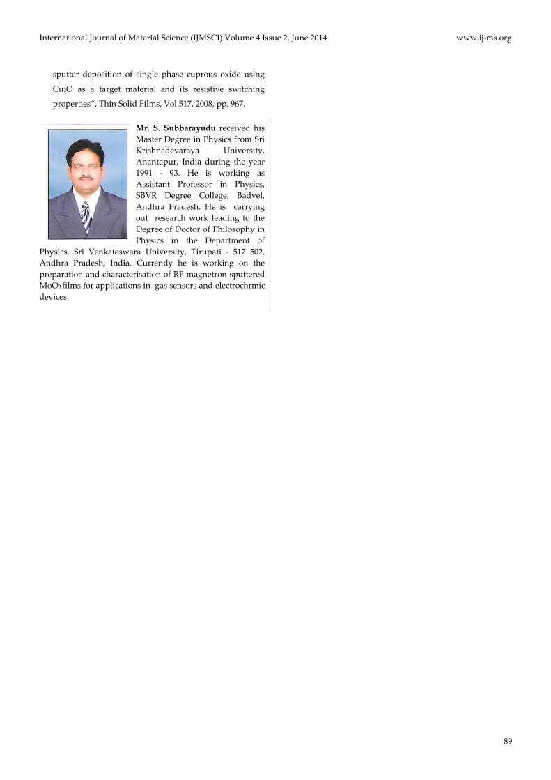
Electrochromic Properties
Figure 13 shows the optical transmittance spectra of colored and virgin (bleached) states of the MoO3 films formed at 303 K and 523 K. The optical modulation, (ΔT %) is the difference of transmittance Tb in bleached and Tc in colored state [(Tb% bleached ) – (Tc% colored)]. The color efficiency (η) at a particular wavelength correlated to the optical contrast can be given by the relation [ Granqvist, 1995],
η = log (Tb/Tc) / (Q/A) = (ΔOD) / (Q/A) (6)
where Tb is the bleaching state transmittance, Tc the colored state transmittance, Q the charge inserted into the films and A the area of the films. The films formed at 303 K showed the virgin state optical transmittance of 53% where as in the colored state it decreased to 38%. The films prepared at 303 K exhibited the optical modulation (at 600 nm), ΔT = 15%. The color efficiency of these MoO3 films was 26 cm2/C. On increasing the substrate temperature to 523 K, the optical transmittance of the virgin state was 87% and at colored state it decreased to 65% with optical modulation of 22%. The color efficiency of the MoO3 films formed at substrate temperature 523 K was increased 30 cm2/C. Thus the optical modulation and coloration efficiency was increase with increase of substrate temperature from 303 K to 523 K. The coloration efficiency of the films deposited at 573 K decreased to 24 cm2/C. The decrease in the coloration efficiency at higher substrate temperature of 573 K may be due to the decrease in the intercalation of Li+ ions during the coloration process. Lin et al. [2010]
85
www.ij-ms.org International Journal of Material Science (IJMSCI) Volume 4 Issue 2, June 2014
reported the coloration efficiency of 25.1 cm2/C for the
films annealed at 573 K. Recently, Madhavi et al. [2013] achieved the optical modulation of 14% and coloration efficiency of 27 cm2/C in thermally oxidized MoO3 films. Sivakumar et al. [2006] reported a maximum coloration efficiency of 30 cm2/C at the wavelength of 633 nm in the films formed at room temperature and it decreased to 14 cm2/C in the films formed at substrate temperature of 473 K, there after it increased to 22 cm2/C at 573 K in electron beam evaporated MoO3 films. The films deposited at 523 K exhibited the better electrochromic properties which will be useful in manufacturing of electrochromism based smart windows.
600 900 1200 15000
20
40
60
80
100
Ts = 303 K bleached Ts = 303 K coloured
Optic
al tra
nsm
ittan
ce (
%)
Wavelength (nm)
(a)
600 900 1200 15000
20
40
60
80
100
Optic
al tra
nsm
ittan
ce (
%)
Wavelength (nm)
(b)
Ts = 523 K bleached Ts = 523 K colored
FIG. 13 OPTICAL TRANSMITTANCE SPECTRA OF COLORED
AND BLEACHED STATE OF MOO3 FILMS FORMED AT SUBSTRATE TEMPERATURES: a) 303 K AND b) 523 K
Conclusions
Thin films of molybdenum oxide were formed on glass and silicon substrates by RF magnetron sputtering of metallic molybdenum target at varying substrate temperatures in the range 303 – 573 K. The deposited films were characterized for their crystallographic structure by X-ray diffraction, surface
morphology with scanning electron microscope and chemical binding configuration by fourier transform infrared spectroscopy. The electrical and optical properties were studied using appropriate methods. The influence of substrate temperature on the structural and surface morphology, electrical and optical properties of the MoO3 films was systematically investigated. The films formed at room temperature (303 K) were X-ray amorphous, and the films formed at 473 K showed the (020) and (040) reflections indicating the growth of α- phase MoO3. The crystallite size of the films increased from 27 nm to 62 nm with increase of substrate temperature. The scanning electron microscope images indicated that the films formed at 303 K were of smooth surface morphology and fine grain structure in amorphous background. The films deposited at substrate temperature of 523 K exhibited the growth of grains with shape of platelets piled one over the other about the size of 1 μm to 1.5 μm. Fourier transform infrared transmittance spectrum of the films formed at 303 K showed broad absorption band between 600 and 1000 cm-1 associated with the charecteristic Mo-O vibrations in the amorphous background. The films formed at 473 K exhibited the bridging and stretching vibrations of Mo = O confirmed the existence of Mo6+ oxidation state related to of phase MoO3. The electrical resistance of the amorphous MoO3 films formed at 303 K was 1.2x10³ Ωcm and at substrate temperature of 523 K it increased to 3.4x10⁴ Ωcm due to the crystalline nature as well as filling of oxygen ion vacancies. The optical band gap of the films increased from 2.98 eV to 3.34 eV with increase of substrate temperature from 303 K to 523 K. The refractive index of the films increased with increase of substrate temperature due to improvement in the crystallinity and packing density of the films. The electro chromic performance of the films was studied on the MoO3 films. Optical modulation of the films increased from 15% to 22% and coloration efficiency increased from 26 cm2/C to 30 cm2/C with increase of substrate temperature from 303 K to 523 K respectively.
REFERENCES
Boudaoud, L.; Benramdana, N.; Desfeux, R.; Khalifa. and B.
Mathieu, C. “Structural and Optical properties of MoO3
and V2O5 thin films prepared by spray pyrolysis”, Catal.
Today, vol 113, 2006, pp. 230.
Bouzidi, A., Benramdane, N., Derraz, H.T., Mathieu, C.,
Khelifa, B. and Desfeux, R., “Effect of substrate
86

International Journal of Material Science (IJMSCI) Volume 4 Issue 2, June 2014 www.ij-ms.org
temperature on the structural and optical properties of
MoO3 thin films prepared by spray pyrolysis technique”,
Mater. Sci. Eng. B, vol 97, 2003, pp. 5.
Comini, E., Foglia, G., Sherveglieri, G., Cantalini, C.,
Passacantano, M., Santace, S., Li, Y., Wlodarski, W. and
Qu, W., “Carbon monoxide response of molybdenum
oxide thin films deposited by different techniques”, Sens.
Actuators B, vol 68, 2008, pp. 168.
Cullity, B.D., Elements of X-ray Diffraction, IInd Ed,
Addison Wesley, London. 1978.
Deb, S.K. and Chopoorian, J.A., “Optical properties and
color-center formation in thin films of molybdenum
trioxide”, J. Appl. Phys., vol 37, 1966, pp. 4818.
Dhanasankar, M.; Purushothaman, K.K. and Muralidharan,
G.,“Effect of temperature and annealing on optical,
structural and electro-chromic properties of sol–gel dip
coated molybdenum oxide films,” Appl. Surf. Sci., vol
257, 2011, pp. 2074.
Eckertova, L., ”Physics of Thin Films” Plenum Press, New
York, 1984.
Elangovan, E., Goncalves, G., Martins, R., Fortunato, E.,” RF
sputtered wide work function indium molybdenum
oxide thin films for solar cell applications,” Solar Energy,
vol 83, 2009, pp. 726.
Fan, X., Fang, G., Qin, P., Sun, N., Liu, N., Zheng, Q.,
Cheng, F., Yuan, L. and Zhao, X., "Deposition
temperature effect of RF magnetron sputtered
molybdenum oxide films on the power conversion
efficiency of bulk- heterojunction solar cells”, J. Phys. D:
Appl. Phys., vol 44, 2011, pp. 045101.
Ghosh, S., Avasthi, D.K., Shah, P., Ganesan, V., Gupta, A.,
Sarangi, D., Bhattacharya, R. and Assmann,
W.,“Deposition of thin films of different oxides of copper
by RF reactive sputtering and their characterization”
Vacuum, Vol 57,2000, pp 377.
Granqvist C.G., Handbook of Inorganic Electro-chromic
Materials, Elsevier, Amsterdam, 1995.
Granqvist, C.G., “Electrochromic tungsten oxide films:
Review of progress 1993–1998,” Solar Energy Mater.
Solar Cells, vol 60, 2000, pp. 201.
Gretener, C.; Perrenoud, J.; Kranz, L.; Baechler, C.; Yoon, S.;
Romanyuk, Y.E.; Buecheler, S. and Tiwari, A.N.
“Development of MoOx thin films As back contact buffer
for CdTe solar cells in substrate configuration”, Thin
Solid Films , vol 535, 2013, pp. 193.
Itoh, T., Matsubara, I., Shin, W., Izu, N. and Nishibori, M.,
“Preparation of layered organic– inorganic nanohybrid
thin films of molybdenum trioxide with polyaniline
derivatives for aldehyde gases sensors of several tens
ppb level,” Sens. Actuators B, vol 128, 2008, pp. 512.
Julien C. M., Pistonia (Ed), Lithium Batteries; New Materials,
Developments and Perspectives, Amsterdam, North
Holland, 1994.
Li, W., Cheng, F., Tao, Z and Chen, J., “Vapor-
transportation preparation and reversible lithium
intercalation/deintercalation of α-MoO3 Microrods”, J.
Phys. Chem. B, vol 110, 2006 pp. 119.
Lin, S.Y., Wang, C.M., Kao, K.S., Chen, Y.C. and Liu, C.C.
“Electrochromic properties of MoO3 thin films derived
by a sol–gel process, J. Sol- gel. Sci. Technol., vol 53,
2010, pp. 51.
Lin, S.Y.; Chen, Y.C., Wang, C.M.; Hseich, P.T.; Shih,
S.C.,“Post-annealing effect upon optical properties of
electron beam evaporated molybdenum oxide thin
films”, Appl. Surf. Sci., vol 255, 2009, pp. 3868.
Madhavi, V., Kondaiah, P., Subbarayudu, S., Hussain O. M.
and Uthanna, S., “Properties of MoO3 films by thermal
oxidation: Annealing induced phase transition”, Mater.
Express, vol 3, 2013, pp. 135.
Mahamad, S.H. and Venkatraj, S., “Thermal stability of
amorphous molybdenum trioxide films prepared at
different oxygen partial pressures by reactive DC
magnetron sputtering”, Vacuum, vol 81, 2007, pp. 636.
Martinez, H.M.; Torres, J.; Lopez Correno, L.D.; Rodriguez-
Garcia, M.E., “Effect of substrate temperature on the
physical properties of molybdenum trioxide thin films
obtained through the spray pyrolysis technique,” Mater.
Character., vol 25, 2013, pp. 184.
Miyata, N. and Akiyoshi, S., “Preparation and
electrochromic properties of RF sputtered molybdenum
oxide films,” J. Appl. Phys., vol 58, 1985, pp. 1651.
Navas, I., Vinodkumar, R., Lethy, K.J., Satyanarayana, M.,
Ganesan, V. and Mahadevan Pillai, V.P., “Enhanced
ethanol sensing response from nanostructured MoO3“, J.
Nanosci. Nanotechnol., vol 9, 2009, pp. 5254.
Navas, I.; Vinod Kumar, R.; Lethy, K.J.; Detty, A.P.;
87

www.ij-ms.org International Journal of Material Science (IJMSCI) Volume 4 Issue 2, June 2014
Ganesan, V.; Sathe, V. and Mahadevan Pillai, V.P.
“Growth and characterization of molybdenum oxide
nanorods by RF magnetron sputtering and subsequent
annealing”, J. Phys. D: Appl. Phys., vol 42, 2009, pp.
175305.
Nazri, G.A., and Julien, C.M.,“Far infrared and Raman
studies of orthorhombic MoO3 single crystal“, Solid State
Ionics, vol 53, 1992, pp. 376. Okumu, J., Koerfer, F.,
Salinga, C., Pedersen, T.P. and Wuttig, M.,
“Gasochromic switching of reactively sputtered
molybdenum oxide films: A correlation between film
properties and deposition pressure,” Thin Solid Films,
vol 515, 2006, pp. 1327.
Patil, R.S.; Uplane, M.D. and Patil, P.S. “Structural and
optical properties of electro-deposited molybdenum
oxide thin films,” Appl. Surf. Sci., vol 252, 2006, pp.
8050.
Patil, R.S.; Uplane, M.D. and Patil, P.S., “Electro-synthesisof
electrochromic molybdenum oxide thin films with rod-
like features”, Int. J. Electrochem. Sci., vol 3, 2008, pp.
259.
Patzke, G.R., Michailovski, A., Krumeich, F., Nesper, R.,
Grunwaldt, J.D. and Baiker, A., “One-step synthesis of
submicrometer fibers of MoO3, Chem. Mater., vol 16,
2004, pp. 1126.
Prasad, A.K., Kubinski, D.J. and Gouma, P.I., “Comparison
of sol–gel and ion beam deposited MoO3 thin film gas
sensors for selective ammonia detection,” Sens.
Actuators B, vol 93, 2003, pp. 25.
Ramana, C.V. and Julien, C.M. “Chemical and
electrochemical properties of molybdenum oxide thin
films prepared by reactive pulsed- laser assisted
deposition”, Chem. Phys. Lett., vol 428, 2006, pp. 114.
Ramana, C.V., Atuchin,V V., Kesler, V. G.,Kochubey,V.A.,
Pokrovsky, L.D., Shutthanandan, V., Becker., U. and
Ewing, R.C., “Growth and surface characterization of
sputter-deposited molybdenum oxide thin films”, Appl.
Surf. Sci., vol. 253, 2007, pp. 5368.
Sabhapathi, V.K., Hussain, O.M., Uthanna, S., Srinivasulu
Naidu, B., Jayarama Reddy, P., Julien, C. and Balkanski,
M., “AC conductivity studies on Al/MoO3/Al sandwich
structures”, Mater. Sci. Eng. B, vol 32, 1995, pp. 93.
Sain, T.S. and Reddy, G.B., “Stoichiometric amorphous
MoO3 films: A route to high performance electrochromic
devices,” J. Appl. Phys., vol 98, 2005, pp. 026104.
Scarminio, J., Lourenco, A., and Gorenstein, A.,
“Electrochromism and photochromism in amorphous
molybdenum oxide films,” Thin Solid Films, vol 302,
1997, pp. 66.
Sian, T.S. and Reddy. G.B., “Optical, structural and
photoelectron spectroscopic studies on amorphous and
crystalline molybdenum oxide thin films,” Solar Energy
Mater. Solar Cells, vol 82, 2004, pp. 375.
Sivakumar, R., Manisankar, P., Jayachandran, M. and
Sanjeeviraja, C., “Intercalation studies on electron beam
evaporated MoO3 films for electrochemical devices”,
Solar Energy Mater. Solar Cells, vol 90, 2006, pp. 2438.
Sivakumar, R.; Gopalakrishnan, R.; Jayachandran, M. and
Sanjeeviraja, C., “Characterization on electron beam
evaporated α- MoO3 thin films by the influence of
substrate temperature,” Curr. Appl. Phys., vol 7, 2007,
pp. 51.
Srinivasa Rao,K,; Rajini Kanth, B. andMukhopadhyay P.K.,
“Optical and IR studies on RF magnetron sputtered
ultra-thin MoO3 films”, Appl. Phys. A, vol 9, 2009, pp.
985.
Tauc, J., ”Amorphous and Liquid Semiconductors”, Plenum
Press, New York, 1974.
Taurino, A. M., Forleo, A., Francioso, L. and Siciliano, P.,
“Influence of doping on the preferen- tial growth of α-
MoO”, Appl. Phys. Lett., vol 88, 2006, pp. 152111.
Uthanna, S.; Nirupama, V. and Pierson, J.F. “Substrate
temperature influenced structural, electrical and optical
properties of dc magnetron sputtered MoO3 films”,
Appl. Surf. Sci., vol 256, 2010, pp. 3133.
Wu, M.C. and Lee, C.S., “α- MoO3 nanocrystals of controlled
size on a glass substrate”, Mater. Res. Bull., vol 44, 2009,
pp. 629.
Yahaya, M., Salleh, M.M. and Talib, I.A., ”Optical properties
of MoO3 thin films for electrochromic windows”, Solid
State Ionics, vol 113, 1998, pp.421.
Yang, W.Q., Wei, Z.R., Zhu, X.H. and Yang, D.Y., “Strong
influence of substrate temperature on the growth of
nanocrystalline MoO3 thin films,” Phys. Lett. A, vol 373,
2009, pp. 3965.
Yang, W.Y., Kim, W.G. and Rhee, S.W., "Radio frequency
88
International Journal of Material Science (IJMSCI) Volume 4 Issue 2, June 2014 www.ij-ms.org
sputter deposition of single phase cuprous oxide using
Cu2O as a target material and its resistive switching
properties“, Thin Solid Films, Vol 517, 2008, pp. 967.
Mr. S. Subbarayudu received his Master Degree in Physics from Sri Krishnadevaraya University, Anantapur, India during the year 1991 - 93. He is working as Assistant Professor in Physics, SBVR Degree College, Badvel, Andhra Pradesh. He is carrying out research work leading to the Degree of Doctor of Philosophy in Physics in the Department of
Physics, Sri Venkateswara University, Tirupati - 517 502, Andhra Pradesh, India. Currently he is working on the preparation and characterisation of RF magnetron sputtered MoO3 films for applications in gas sensors and electrochrmic devices.
89