Embed Size (px)
Citation preview
III-241
Abstract: Substrate effects in complete design models forHBT’s in IC’s are identified by a one-step model extrac-tion processes that, unlike most other known substrate ef-fect identification procedures, does not require initial testsubstrate preparations. The method identifies and quanti-fies substrate effect components that are important for in-terstage designs and distinguish them from less importantsubstrate capacitances and losses in probe pads.
1 Introduction
Accurate modelling is a prerequisite for broadband de-sign of RF IC’s. Initial trials with a commercial SiGeHBT process for designing L-band modulators and de-modulators in radar applications, where the require-ments are 400MHz and/or 800 MHz phase linear signalbandwidth around carriers, have shown that we mustsupply substrate effects to the model that the vendorprovides. Unlike other small signal modelling ap-proaches and more theoretical investigations [ 1], theone that is used in this work does not rely upon separatetest-jig substrate identifications followed by a subse-quent model deembedding process. Instead all compo-nents in the complete equivalent circuits are identifiedin one step. Here we employ an extraction process,which utilizes uncertainty data from measurements inconjunction with the model network sensitivity matrix.
It gives us at tool by which we fast and efficiently maysurvey and select model structures that stay stable andconsistent across the required operating range of thetransistors. The basic method was originally developedin [ 2], and has proved successful in a series of model-ling tasks including the one discussed in [ 3].
2 Model Structures ,
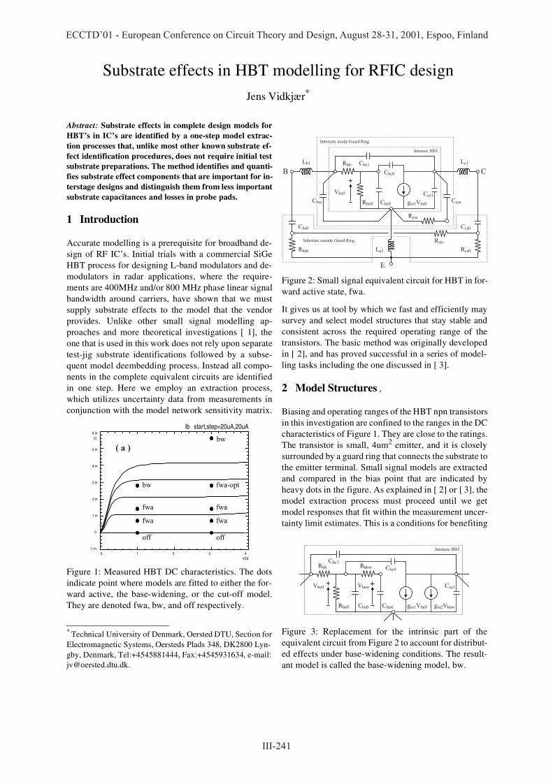
Biasing and operating ranges of the HBT npn transistorsin this investigation are confined to the ranges in the DCcharacteristics of Figure 1. They are close to the ratings.The transistor is small, 4um2 emitter, and it is closelysurrounded by a guard ring that connects the substrate tothe emitter terminal. Small signal models are extractedand compared in the bias point that are indicated byheavy dots in the figure. As explained in [ 2] or [ 3], themodel extraction process must proceed until we getmodel responses that fit within the measurement uncer-tainty limit estimates. This is a conditions for benefiting
Ib start,step=20uA,20uA
0. 1. 2. 3. 4.VCE
-1.m
0.
1.m
2.m
3.m
4.m
5.m
6.mIC
( a )
bw
fwa
fwa
off
fwa-opt
fwa
fwa
off
bw
* Technical University of Denmark, Oersted DTU, Section forElectromagnetic Systems, Oersteds Plads 348, DK2800 Lyn-gby, Denmark, Tel:+4545881444, Fax:+4545931634, e-mail:[email protected].
Figure 1: Measured HBT DC characteristics. The dotsindicate point where models are fitted to either the for-ward active, the base-widening, or the cut-off model.They are denoted fwa, bw, and off respectively.
Cbs0
Rbs0
Ccs0
Rcs0
Rsio
Rcss
Lc1Lb1
Le1
Cbss CcssCbe0
Cbc0
Cbc1
Cce1
gm1Vbe0
Vbe0
Rbe0
Rbb
Intrinsic HBT
Substrate inside Guard Ring
Substrate outside Guard Ring
B C
E
Figure 2: Small signal equivalent circuit for HBT in for-ward active state, fwa.
CbewCbe0
Cbc0
Cbc1
Cce1
gm1Vbe0 gm2Vbew
Vbe0 Vbew
Rbe0
Rbb Rbbw
Intrinsic HBT
Figure 3: Replacement for the intrinsic part of theequivalent circuit from Figure 2 to account for distribut-ed effects under base-widening conditions. The result-ant model is called the base-widening model, bw.
Substrate effects in HBT modelling for RFIC design
Jens Vidkjær*
ECCTD’01 - European Conference on Circuit Theory and Design, August 28-31, 2001, Espoo, Finland

III-242
from sensitivity matrix data. To achieve this goal in allselected bias point, three model topologies were re-quired, one for the normal forward operation, one athigh currents where base-widening effects may besensed so a distributed description of the carrier trans-port through the base is required. Finally a model thatapplies to the cut-off operation with zero DC current.The models are referred to as “fwa”, “bw”, and “off” re-spectively and they are detailed in Figure 2, Figure 3,and Figure 4. Examples of the fitting accuracies for eachtype of model are illustrated in Figure 5
3 Parameter Extractions
Only the forward active model in Figure 2 shows thecomplete equivalent circuit. As seen here, the model issubdivided into a section representing intrinsic HBT op-
erations, which is encircled by three components, C bss,Ccss,and Rcss, that represent substrate effects inside theguard ring and beneath the transistor. Finally, the tran-sistor connections to the terminal probe pads are de-scribed by small series inductances, pad to substratecapacitances and substrate losses outside the transistor.The important point in the process of identifying sub-strate effects is that only the intrinsic part of the modelneeds substitution between the different mode of opera-tions. Model topologies for substrate effects both insideand outside the guard ring and for the transistor leads re-main the same in all cases with reasonably stable com-ponent values across all the operating points.
To elaborate this point further, Table 1 summarizesmodel extraction data for a forward active situation.Shown here is a column of resultant component valuesand then two columns with intersection and relative de-viation data. They are derived from the sensitivity ma-trix by singular value decomposition and summarizestatistical estimates for the parameter values. The inter-section column data are interpreted as the relative devi-ation for each particular parameter if all otherparameters were precisely extracted. In contrast, the rel-ative deviation parameters, which are always higher,take into account mutual correlations between all pa-rameters in the model extraction process. The ratio be-tween these two figures give a simple estimate of howindependent a given parameter is. Scanning trough the
Cbe0
Cbc1
Cce1
Rbe0
Rbb
Intrinsic HBT
Figure 4: Replacement of the intrinsic part of the equiv-alent circuit from Figure 2 if the transistor is cut-off.The complete model is called the cut-off or off model.
phase
phase
( a ) ( b ) ( c )
phase
phase
phase
phase
mag.mag.
mag.
mag. mag.
mag.
Figure 5: Examples of model fitting in (a) cut off at 3V,0mA, (b) forward active at 3V,2.8 mA, and (c) base-wid-ening at 3V,5.6 mA. Each set of magnitude or phase curves holds four entities. First points of measured data se-lected as targets in fits, 2nd, a center curve showing fitted model responses, 3rd, the upper and, 4th, the lower99.9% uncertainty estimates of the network analyzer and probe station setup.

III-243
table, the general pattern - with two prominent excep-tions - is, that if we moves from the intrinsic transistoroutwards through the guard ring to the pads, we simul-taneously goes from accurately determined componentsto more and more uncertain and cross correlated compo-nents. The two exceptions are the intrinsic feed-back ca-pacitance Cbc0, which is highly correlated by the largeroverlay capacitance Cbc1 and, therefore, more uncer-tain. The other exception is the common emitter lead in-ductance Le1 that is accurately determined due to itsstrong influence upon both gain and feed-back in thetransistor.
If a component in the model shows a relative devia-tions of more than 100%, it should be left out, especiallyif it correlates with other parts of the model. Otherwiseit convoys uncertainty to other components. This obser-vation is the fact behind the employment three modelsinstead of one in the present HBT model extraction. Inprinciple, the base-widening intrinsic circuit from Fig-ure 3 contains all circuit components that are present inthe other two intrinsic models. However, componentsthat are superfluous in the forward active or the cut-offcases make the complete base-widening equivalent cir-
cuit useless here because uncertainty will spread also toimportant parameters. This leaving out approach is akey to the present extraction method, since it gives a fastway of surveying and selecting model topologies thatsuit a given set of experimental data.
4 Substrate Effects
Substrate effects from inside the guard ring are often themost important in a design process, since they arepresent in all transistors. Their significance are illustrat-ed by Figure 6. It is clearly observed that the design kitmodel responses differ from actual measured data. Insome respects, like the difference in S21 magnitudes, thedifference may be ascribe to process tolerance. It is alsoseen that the S11 and S21 roll-off frequencies are nearlythe same in both design kit data and measurements. Thisis, however, not the case with the two other magnitudes,S12 and S22, a fact that is illuminated further by the thirdset of curves denoted “inside model”. This set showssimulated responses from the parts of the fitted modelsthat hold the intrinsic HBT and substrate effects frominside the guard rings, but leaves out effects of lead in-ductances and substrate outside the guard rings accord-ing to the subdivision in Figure 2. Including the effectsfrom inside the guard ring we clearly get much more re-alistic frequency dependencies of both the transistorfeed-back effects and the output impedances throughS12 and S22. To be more accurate in the design phase,each transistor should therefore be surrounded by ele-ments from the model identifications above that have nocounterparts in the vendor supplied design kit models.This is firstly the substrate effects from inside the guardring but, surprisingly, the overlay diode capacitanceCbc1 should also be included. Table 2 summarizes the
Parm. ValueIntersc
%Rel.
dev %
Rbb 102.6 .25 1.55
Cbc0 2.2231f 3.75 21.93
Cbe0 493.36f .21 1.59
Rbe0 824.43 .99 2.31
Gm1 60.008m .15 .40
Cbc1 8.2417f .57 2.09
Cce1 59.088f .94 2.92
Cbss 70.782f .78 1.52
Ccss 136.96f 1.04 8.64
Rcss 247.97 .93 3.75
Lb1 198.15p 2.10 5.42
Lc1 150.83p 5.33 13.97
Le1 115.28p .77 1.88
Cbs0 115.95f 3.98 8.78
Rbs0 1.5869K 2.85 15.15
Ccs0 141.34f 2.82 9.50
Rcs0 931.74 1.92 19.08
Rsio 17.984K 2.51 9.26
Table 1 Extracted parameter values and their sta-tistical data for the forward active HBT model at 3V, 2.8mA.
modeltype
VceV
IcmA
Cbc1fF
CbssfF
CcssfF
RcssOhm
co 1 0.0 11.3 73.8 172. 282.
fwa 1 0.7 10.5 51.2 179. 249.
fwa 1 1.4 10.6 60.8 159. 235.
bw 1 2.8 9.1 54.1 170. 251.
co 3 0.0 9.9 74.2 176. 288.
fwa 3 0.7 8.7 51.5 183. 257.
fwa 3 1.4 8.6 59.7 169. 243.
fwa 3 2.8 8.2 70.8 137. 248.
bw 3 5.6 6.4 54.9 218. 247.
Table 1 Substrate and overlay elements inside guard ring in all parameter extractions. Model types refer to Figure 1 to 4.

III-244
corresponding extracted component values. They stayreasonably constant across all investigated bias pointsdespite large differences in operating modes. In a designprocess they may safely be included as constant values.
Comparing the measured and fitted magnitude datain Figure 6 with the corresponding responses from themodel inside the guard ring shows that substrate lossesoutside the guard ring mostly influences the magnitudeof S22. The most prominent effects from regions outsidethe guard ring are, however, the phase shifts that are in-troduced by lead inductances and pad capacitors. Theireffects are significant for the experimental identifica-tion process and must be known there. This part of themodel is, on the other hand, not of same great impor-tance for design, because it contributes nothing to inter-stage connections inside circuits on the same chip. It isconsequently not a severe limitation that most of themodel components outside the guard ring are deter-mined with large tolerances compared to the tolerancesof components inside the guard ring and in the intrinsicHBT model.
5 Conclusions
The paper has demonstrated how substrate effects in aHBT process may be experimentally identified by a di-
rect one-step model identification process, which owesits accuracy to systematic use of measurement uncer-tainty data and the sensitivity matrix of the model ex-traction process. The method identifies importantsubstrate parameters for interstage designs and providecircuit elements, that may be used directly around thevendor supplied design models to get more realisticsimulations.
References
[ 1] M.Pfost,H.-M.Rein, Modelling and measurementof substrate coupling in Si-MMIC’s up to 40 GHz.IEEE j.Solid State Circuits, vol.33, no.4,pp582-591,Apr.1998
[ 2] J.Vidkjær, Accuracy Bounds in Small-Signal Mod-el Identification, Proc. 10th European Conf. CircuitTheory and Design, Sep.2-6, pp.782-791, 1991.
[ 3] V.Porra, J.Vidkjær, T.Brazil, Non-linear dynamicmodelling of RF bipolar transistors, in G.A.S.Mach-ado ed. “Low-Power HF Microelectronics, a unifiedapproach”, Chap.8 pp 301-331, IEE Circuits andSystems Series 8, 1996.
Figure 6: Differences between s-parameters from the vendors design kit, measured/fitted data, and responses fromthat part of the fitted model that holds intrinsic functions and substrate effects inside the guard ring. All curves inthis example apply to the forward active data at 3V, 2.8mA bias
magnitudes phases
fittet/measured
fittet/measured
fittet/measured
fittet/measured
inside model
inside model
inside modelinside model
design kit model
design kit model
design kit model
design kit model
fittet/measured
fittet/measured fittet/measured
fittet/measuredinside model
inside model inside model
inside modeldesign kit model
design kit model design kit model
design kit model