Embed Size (px)
Citation preview
Sub-microsecond Adaptive Voltage Scaling in a 28nm FD-SOI Processor SoC
Ben Keller*, Martin Cochett*, Brian Zimmer*, Yunsup Lee*, Milovan Blagojevict*,
Jaehwa Kwak*, Alberto Puggelli*, Stevo Bailey*, Pi-Feng Chiu*, Palmer Dabbelt*,
Colin Schmidt*, Elad Alon*, Krste Asanovi6*, Borivoje NikoliC* Email: [email protected]
* Department of Electrical Engineering and Computer Sciences, University of California, Berkeley, CA, USA t STMicroelectronics, Crolles, France
Abstract-This work presents a RISC-V system-on-chip (SoC) with integrated voltage regulation and power management implemented in 28nm FD-SOI. A fully integrated switched-capacitor DC-DC converter, coupled with an adaptive clocking system, achieves 82-89% system conversion efficiency across a wide operating range, yielding a total system efficiency of 41.8 doubleprecision GFLOPSfW. Measurement circuits can detect changes in processor workload and an integrated power management unit responds by adjusting the core voltage at sub-microsecond timescales. The power management system reduces the energy consumption of a synthetic benchmark by 39.8% with negligible performance penalty and 2.0% area overhead, enabling extremely fine-grained «IJLs) adaptive voltage scaling for mobile devices.
I. INTRODUCTION
Mobile and loT devices are energy-constrained and have highly variable workloads. These devices therefore benefit greatly from adaptive voltage scaling (AVS), which improves energy efficiency by scaling voltage as workload varies. Many workloads demonstrate rapid changes in program behavior [1] [2], so AVS is most effective when the voltage setting changes as quickly as possible in response to changing workload. However, traditional SoCs employ off-chip regulators and discrete power management systems that can respond only at timescales of hundreds of microseconds or longer [3].
This work presents a processor system-on-chip (SoC) with integrated voltage regulation and power management. The system includes a fully-featured processor tightly coupled with fully integrated voltage regulators. A programmable power controller can implement a wide range of algorithms that sense and respond at sub-microsecond timescales, enabling fully autonomous power management running entirely in hardware to improve system energy efficiency.
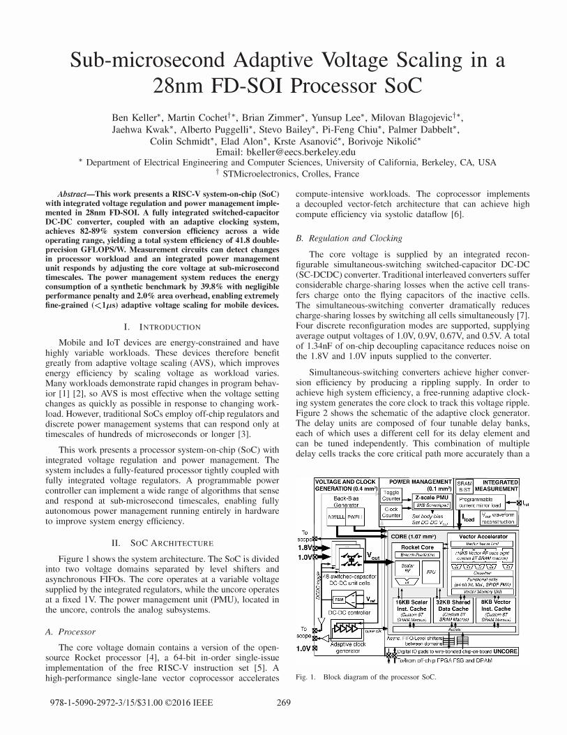
II. SoC ARCHITECTURE
Figure 1 shows the system architecture. The SoC is divided into two voltage domains separated by level shifters and asynchronous FIFOs. The core operates at a variable voltage supplied by the integrated regulators, while the uncore operates at a fixed 1 V The power management unit (PMU), located in the uncore, controls the analog subsystems.
A. Processor
The core voltage domain contains a version of the opensource Rocket processor [4], a 64-bit in-order single-issue implementation of the free RISC-V instruction set [5]. A high-performance single-lane vector coprocessor accelerates
978-1-5090-2972-3/15/$31.00 ©20 16 IEEE 269
compute-intensive workloads. The coprocessor implements a decoupled vector-fetch architecture that can achieve high compute efficiency via systolic dataflow [6].
B. Regulation and Clocking
The core voltage is supplied by an integrated reconfigurable simultaneous-switching switched-capacitor DC-DC (SC-DCDC) converter. Traditional interleaved converters suffer considerable charge-sharing losses when the active cell transfers charge onto the flying capacitors of the inactive cells. The simultaneous-switching converter dramatically reduces charge-sharing losses by switching all cells simultaneously [7]. Four discrete reconfiguration modes are supported, supplying average output voltages of 1.0V, 0.9V, O.67V, and O.5V A total of 1.34nF of on-chip decoupling capacitance reduces noise on the 1.8V and 1.0V inputs supplied to the converter.
Simultaneous-switching converters achieve higher conversion efficiency by producing a rippling supply. In order to achieve high system efficiency, a free-running adaptive clocking system generates the core clock to track this voltage ripple. Figure 2 shows the schematic of the adaptive clock generator. The delay units are composed of four tunable delay banks, each of which uses a different cell for its delay element and can be tuned independently. This combination of multiple delay cells tracks the core critical path more accurately than a
Fig. 1. Block diagram of the processor Soc.
Fig. 2. Block diagram of the adaptive clock generator.
single standard cell type [8]. Because high system conversion efficiency depends on accurate instantaneous tracking of the critical path, care was taken during physical design to minimize the insertion delay from the output of the adaptive clock generator to the core clock sinks.
C. Integrated Power Management
The uncore contains a PMU processor, an implementation of the 32-bit RISC-V Z-scale microcontroller with an 8KB scratchpad memory [9]. The PMU can read and write control registers for other subsystems on the SoC, including the SCDCDC converter setting, and communicates directly with the compute processor via interprocessor interrupts. The PMU is fully programmable via the RISC-V C compiler. Figure 3 compares the two processors in the Soc.
Switching of the SC-DCDC converter is triggered by comparison of the output voltage to a fixed lower-bound reference. For a particular SC-DCDC configuration and reference voltage, each switching event transfers a fixed amount of charge at a known voltage and so corresponds to a fixed amount of energy consumed. The frequency of the SC-DCDC toggle signal can therefore be used to measure core power with minimal overhead. Integrated measurement logic synchronizes the SC-DCDC toggle signal to a 1GHz reference and counts the number of toggles that occur during a reference duration to measure near-instantaneous power consumption. This approach is simpler and less disruptive than previous energy measurement schemes, which place a sense resistor between the supply and the load [10] or halt the normal operation of
Fig. 3. Key features of the integrated processors.
270
Fig. 4. Integrated power management system that can infer power consumption and change voltage modes according to a program.
the voltage regulators to measure current draw [11]. A separate counter synchronizes and measures the average frequency of the adaptive core clock, allowing for real-time frequency monitoring. The results of these measurements can be read by the PMU. The counters and PMU together occupy just 0.062mm2 (2.0% of die area).
Taken together, the PMU, counters, and integrated SCDCDCs can implement power-management algorithms such as frequency hopping and adaptive voltage scaling entirely on-die. Figure 4 summarizes this control loop, which can operate at very fast timescales because it does not involve any off-chip components or communication.
III. ME ASUREMENT RESULTS
The chip is implemented in 28nm ultra-thin body and BOX fully-depleted silicon-on-insulator (UTBB FD-SOI) technology [12]. Figure 5 shows an annotated die photo and a summary of key features. The chip is wirebonded directly onto a custom PCB, which is mounted onto a motherboard for test. A Xilinx ZedBoard communicates with the chip and acts as backing memory for the processor subsystem.
A. SoC Peiformance
Figure 6 shows the processor functionality across a wide voltage range. The SC-DCDC converter is placed into bypass mode for characterization, allowing measurement of processor performance under fixed voltage and frequency.
Figure 7 shows the best frequency achievable at each operating point and the total energy consumed by a fixed-duration matrix-multiply benchmark at that operating point. The application of forward body bias (FBB) increases performance
Fig. 5. Annotated die micrograph and chip summary.
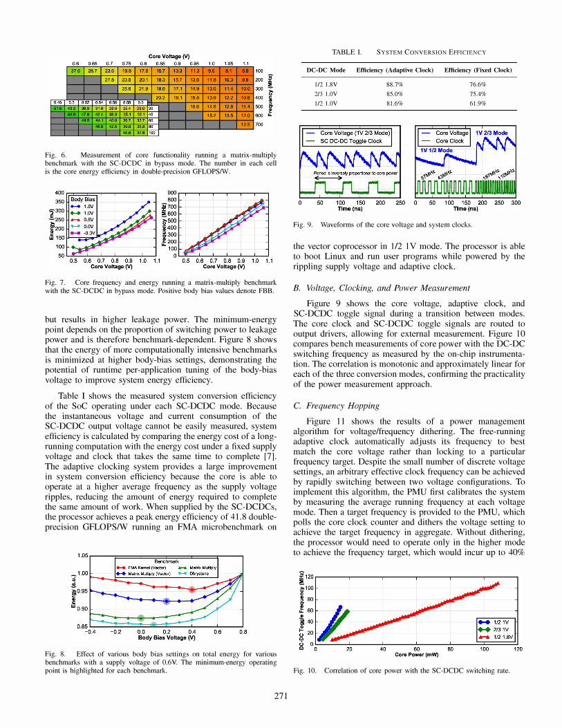
Fig. 6. Measurement of core functionality running a matrix-multiply benchmark with the SC-DCDC in bypass mode. The number m each ceU is the core energy efficiency in double-precision GFLOPSIW.
Fig. 7. Core frequency and energy running a matrix-multiply benchmark with the SC-DCDC in bypass mode. Positive body bias values denote FBB.
but results in higher leakage power. The minimum-energy point depends on the proportion of switching power to leakage power and is therefore benchmark-dependent. Figure 8 shows that the energy of more computationally intensive benchmarks is minimized at higher body-bias settings, demonstrating the potential of runtime per-application tuning of the body-bias voltage to improve system energy efficiency.
Table I shows the measured system conversion efficiency of the SoC operating under each SC-DCDC mode. Because the instantaneous voltage and current consumption of the SC-DCDC output voltage cannot be easily measured, system efficiency is calculated by comparing the energy cost of a longrunning computation with the energy cost under a fixed supply voltage and clock that takes the same time to complete [7]. The adaptive clocking system provides a large improvement in system conversion efficiency because the core is able to operate at a higher average frequency as the supply voltage ripples, reducing the amount of energy required to complete the same amount of work. When supplied by the SC-DCDCs, the processor achieves a peak energy efficiency of 41.8 doubleprecision GFLOPS/w running an FMA microbenchmark on
Fig. 8. Effect of various body bias settings on.
total energy for various benchmarks with a supply voltage of O.6Y. The mInimum-energy operatmg point is highlighted for each benchmark.
271
TABLE l. SYSTEM CONVERSION EFFICIENCY
DC-DC Mode Efficiency (Adaptive Clock) Efficiency (Fixed Clock) 1/2 1.8V 88.7% 76.6% 2/3 1.0V 85.0% 75.4% 1/2 1.0V 81.6% 61.9%
Fig. 9. Waveforms of the core voltage and system clocks .
the vector coprocessor in 112 1 V mode. The processor is able to boot Linux and run user programs while powered by the rippling supply voltage and adaptive clock.
B. Voltage, Clocking, and Power Measurement
Figure 9 shows the core voltage, adaptive clock, and SC-DCDC toggle signal during a transition between modes. The core clock and SC-DCDC toggle signals are routed to output drivers, allowing for external measurement. Figure 10 compares bench measurements of core power with the DC-DC switching frequency as measured by the on-chip instrumentation. The correlation is monotonic and approximately linear for each of the three conversion modes, confirming the practicality of the power measurement approach.
C. Frequency Hopping
Figure 11 shows the results of a power managem�nt algorithm for voltage/frequency dithering. The free-runmng adaptive clock automatically adjusts its frequency to best match the core voltage rather than locking to a particular frequency target. Despite the small number of discrete v�ltage settings, an arbitrary effective clock frequency can be �chleved by rapidly switching between two voltage configuratIOns. To implement this algorithm, the PMU first calibrates the system by measuring the average running frequency at each volt�ge mode. Then a target frequency is provided to the PMU, which polls the core clock counter and dithers the v?ltage s�ttin� to achieve the target frequency in aggregate. Without dlthenng, the processor would need to operate only in the higher mode to achieve the frequency target, which would incur up to 40%
Fig. 10. Correlation of core power with the SC-DCDC switching rate.
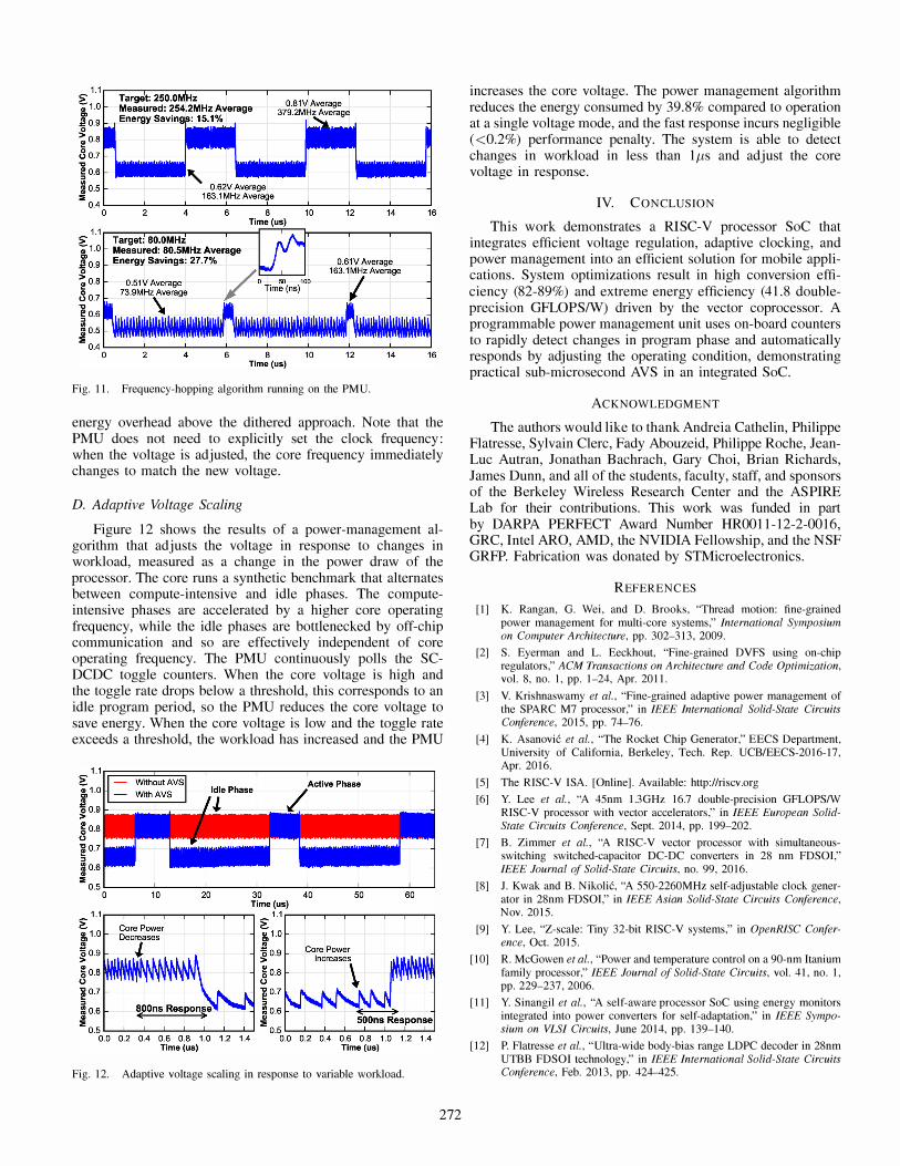
Fig. 11. Frequency-hopping algorithm running on the PMU.
energy overhead above the dithered approach. Note that the PMU does not need to explicitly set the clock frequency: when the voltage is adjusted, the core frequency immediately changes to match the new voltage.
D. Adaptive Voltage Scaling
Figure 12 shows the results of a power-management algorithm that adjusts the voltage in response to changes in workload, measured as a change in the power draw of the processor. The core runs a synthetic benchmark that alternates between compute-intensive and idle phases. The computeintensive phases are accelerated by a higher core operating frequency, while the idle phases are bottle necked by off-chip communication and so are effectively independent of core operating frequency. The PMU continuously polls the SCDCDC toggle counters. When the core voltage is high and the toggle rate drops below a threshold, this corresponds to an idle program period, so the PMU reduces the core voltage to save energy. When the core voltage is low and the toggle rate exceeds a threshold, the workload has increased and the PMU
Fig. 12. Adaptive voltage scaling in response to variable workload.
272
increases the core voltage. The power management algorithm reduces the energy consumed by 39.8% compared to operation at a single voltage mode, and the fast response incurs negligible ( <0.2%) performance penalty. The system is able to detect changes in workload in less than Ip,s and adjust the core voltage in response.
IV. CONCLUSION
This work demonstrates a RISC-V processor SoC that integrates efficient voltage regulation, adaptive clocking, and power management into an efficient solution for mobile applications. System optimizations result in high conversion efficiency (82-89%) and extreme energy efficiency (41.8 doubleprecision GFLOPSIW) driven by the vector coprocessor. A programmable power management unit uses on-board counters to rapidly detect changes in program phase and automatically responds by adjusting the operating condition, demonstrating practical sub-microsecond AVS in an integrated Soc.
ACKNOW LEDGMENT
The authors would like to thank Andreia Cathelin, Philippe Flatresse, Sylvain Clerc, Fady Abouzeid, Philippe Roche, JeanLuc Autran, Jonathan Bachrach, Gary Choi, Brian Richards, James Dunn, and all of the students, faculty, staff, and sponsors of the Berkeley Wireless Research Center and the ASPIRE Lab for their contributions. This work was funded in part by DARPA PERFECT Award Number HROOll-12-2-0016, GRC, Intel ARO, AMD, the NVIDIA Fellowship, and the NSF GRFP. Fabrication was donated by STMicroelectronics.
REFERENCES
[1] K. Rangan, G. Wei. and D. Brooks. "Thread motion: fine-grained power management for multi-core systems," International Symposium on Computer Architecture, pp. 302-313, 2009.
[2] S. Eyerman and L. Eeckhout, "Fine-grained DVFS using on-chip regulators," ACM Transactions on Architecture and Code Optimization, vol. 8, no. I, pp. 1-24, Apr. 2011.
[3] V. Krishnaswamy et al., "Fine-grained adaptive power management of the SPARC M7 processor," in IEEE International Solid-State Circuits Conference, 2015, pp. 74-76.
[4] K. Asanovic et aI., "The Rocket Chip Generator," EECS Department, University of California, Berkeley, Tech. Rep. UCB/EECS-2016-17, Apr. 2016.
[5] The RISC-V ISA. [Online]. Available: http://riscv.org
[6] y. Lee et aI., "A 45nm 1.3GHz 16.7 double-precision GFLOPS/W RlSC-V processor with vector accelerators," in IEEE European SolidState Circuits Conference, Sept. 2014, pp. 199-202.
[7] B. Zimmer et aI., "A RlSC-V vector processor with simultaneousswitching switched-capacitor DC-DC converters in 28 nm FDSOl," IEEE Journal of Solid-State Circuits, no. 99, 2016.
[8] J. Kwak and B. Nikolic, "A 550-2260MHz self-adjustable clock generator in 28nm FDSOl," in IEEE Asian Solid-State Circuits Conference, Nov. 2015.
[9] Y. Lee, "Z-scale: Tiny 32-bit RlSC-V systems," in OpenRISC Conference, Oct. 2015.
[10] R. McGowen et al., "Power and temperature control on a 90-nm Itanium family processor," IEEE Journal of Solid-State Circuits, vol. 41, no. I, pp. 229-237, 2006.
[II] Y. Sinangil et aI., "A self-aware processor SoC using energy monitors integrated into power converters for self-adaptation," in IEEE Symposium on VLSI Circuits, June 2014, pp. 139-140.
[12] P. Flatresse et aI., "Ultra-wide body-bias range LDPC decoder in 28nm UTBB FDSOI technology," in IEEE International Solid-State Circuits Conference, Feb. 2013, pp. 424-425.