Embed Size (px)
Citation preview
OPEN
ARTICLE
SU8 etch mask for patterning PDMS and its application toflexible fluidic microactuatorsBenjamin Gorissen1, Chris Van Hoof2, Dominiek Reynaerts1 and Michael De Volder1,3
Over the past few decades, polydimethylsiloxane (PDMS) has become the material of choice for a variety of microsystemapplications, including microfluidics, imprint lithography, and soft microrobotics. For most of these applications, PDMS is processedby replication molding; however, new applications would greatly benefit from the ability to pattern PDMS films using lithographyand etching. Metal hardmasks, in conjunction with reactive ion etching (RIE), have been reported as a method for patterning PDMS;however, this approach suffers from a high surface roughness because of metal redeposition and limited etch thickness due to pooretch selectivity. We found that a combination of LOR and SU8 photoresists enables the patterning of thick PDMS layers by RIEwithout redeposition problems. We demonstrate the ability to etch 1.5-μm pillars in PDMS with a selectivity of 3.4. Furthermore, weuse this process to lithographically process flexible fluidic microactuators without any manual transfer or cutting step. The actuatorachieves a bidirectional rotation of 50° at a pressure of 200 kPa. This process provides a unique opportunity to scale down theseactuators as well as other PDMS-based devices.
Keywords: PDMS lithography; SU8; etch mask; microactuator; bending actuator; fluidic actuator
Microsystems & Nanoengineering (2016) 2, 16045; doi:10.1038/micronano.2016.45; Published online: 12 September 2016
INTRODUCTIONPolydimethylsiloxane (PDMS) is one of the most versatile materialsfor fabricating microsystems1. Simple replication molding2 allowsreplicating features as small as 0.4 nm (Ref. 3) and structures withaspect ratios exceeding 50:1 (Ref. 4). Furthermore, PDMS can bebonded to itself, silicon wafers, and glass slides by a straightfor-ward oxygen–plasma process5. These properties have been keyfor scientific progress in important fields of research, includingmicrofluidics and imprint lithography. Although most currentPDMS devices are fabricated using replication molding, emergingdomains such as soft robotics6–9 require, on one hand, the abilityto shape PDMS by molding or by selective curing and, on theother hand, the ability to locally remove PDMS. The latter iscurrently often performed manually by locally cutting awaymaterial with a scalpel. This process is both inaccurate and slow,and therefore, more integrated lithography-based processes usingetching would enable further scaling down of soft robotic systemsto micrometer sizes to enable new applications of PDMS devices.Several research groups demonstrated the ability to dry etch
PDMS using fluorine-based plasmas that are able to break downthe Si–O backbone of PDMS10,11. However, the aluminum andgold hardmasks that are used cause high surface roughness, mostlikely by re-sputtering the etch mask material12 and a mismatch inthe thermal expansion coefficient between PDMS and the metalmask13.Instead of metal etch masks, we suggest using SU8 photoresist
(MicroChem, Westborough, MA, USA) as an etch mask inconjunction with a sacrificial release layer. Both SU8 and PDMSare etched by RIE with a mixture of CF4/SF6 and O2, but the gas
composition for efficient PDMS etching is different for SU8 (Ref.14). Furthermore, an important advantage of SU8 masks is thatthey can be patterned in thick layers (4200 μm) with aspect ratiosover 20 (Ref. 15), allowing long etch times. A disadvantage of SU8masks is that they are very difficult to remove after the etchingprocess. Thus, we developed a process using a thin sacrificial lift-off resist (LOR; MicroChem) layer that is etched afterwards torelease the SU8 masks. Previous research16 suggests using SU8 asa mask but provides no solution for the removal of the etch mask.By introducing the sacrificial LOR-layer, the SU8 masking layer canbe easily removed, which is important for most applicationsbecause the SU8 mask or over-etching are undesirable.A typical example of a soft robotic device requiring structuring
of PDMS is flexible pneumatic bending actuators that are usedto execute delicate tasks such as handling biological tissues that isimpossible using traditional rigid robots8,17–21. These actuatorsshow a large bending deformation when pressurized and isused as a demonstrator in this paper. In their most straight-forward configuration, they consist of an inflatable voidsurrounded by an asymmetric flexible structure consisting, forinstance, of two bonded PDMS layers with different thicknesses22.To date, these actuators are typically fabricated by a combinationof replication molding and manual cutting; this type of fabricationlimits the size of the actuators as well as the fabricationthroughput. Here we demonstrate how the proposed SU8/LORetch mask can be used to replace this manual process, thusenabling opportunities for further miniaturization of these PDMSdevices.
1Department of Mechanical Engineering, Katholieke Universiteit Leuven & Flanders Make, Celestijnenlaan 300B, 3001 Leuven, Belgium; 2Imec, Kapeldreef 75, 3001 Leuven,Belgium and 3Institute for Manufacturing, Department of Engineering, University of Cambridge, 17 Charles Babbage Road, Cambridge, CB3 0FS, UK.Correspondence: Michael De Volder ([email protected] or [email protected])Received: 14 March 2016; revised: 10 May 2016; accepted: 24 May 2016
Microsystems & Nanoengineering (2016) 2, 16045; doi:10.1038/micronano.2016.45
www.nature.com/micronano
MATERIALS AND METHODSIn the literature, a fluorine-based plasma has been suggested todismantle the silicon-oxygen backbone of PDMS making itpossible to etch it with typical etch parameters summarized inTable 1. Vlachopoulou et al.23 used pure SF6 as an etchantand yielded an etch rate of 48 μm h− 1. The addition of O2 to theetch gas was found to decrease the PDMS etch rate. However,Garra et al.12, Oh et al.11, Bjørnsen et al.24, and Szmigiel et al.25
indicated that a small amount of O2 allows an increase in the etchrate. According to Oh, O2 might increase the number ofreactive fluorine atoms present in the plasma. Szmigiel, however,stated that O2 is used to activate the surface of PDMSbecause of oxidation of the methyl-groups in PDMS:
CxHy solidð Þ þ O2 gasð Þ�!plasma
CO gasð Þ þ H2OðgasÞThese authors also showed that there is a positive correlationbetween etch rate and reactor power. An overall maximum etchrate (72 μm h− 1) was achieved by Szmigiel et al.25 using a 3:1 ratioof SF6 to O2. Alternatively, Tserepi et al.
26 used SF6 together withinert He to achieve an etch rate of 72 μm h− 1.The most commonly used hardmask for RIE processing of PDMS
is aluminum12,23,25. Using this hardmask, poor surface roughnessof both the exposed and non-exposed PDMS parts was observed.The exposed PDMS was deteriorated by resputtering thealuminum-masking layer, and excessive wrinkling could be seenon the masked PDMS because of a mismatch in the thermalexpansion coefficient, as reported by Cristea et al.13. In anotherapproach, normal photoresists were used as a masking layer11,26.These resist layers were all affected by the RIE process with aselectivity ranging between 4.5 and 0.09 (etch rate PDMS/etch ratemasking material). Because masking layer thicknesses are on theorder of a few micrometers, only limited layer thicknesses of PDMScan be etched before the photoresist etch masks deteriorated.To etch thick layers of PDMS while maintaining a good surface
roughness, SU8/LOR is proposed in this paper as a masking layer. SU8has the advantage that it can provide thick high aspect ratio masks.Because SU8 consists of a chain of hydrocarbon bonds, it will beaffected by the oxygen plasma27. In optimal conditions (5% SF6 and95% O2), a SU8 etch rate of 120 μmh−1 can be achieved14; however,this etch ratio shows a steep decline as the volume percentage of SF6increases, which is then in turn very effective for etching PDMS. Thisdifference in optimal gas composition makes SU8 a good candidatefor the masking material for PDMS reactive ion etching using a largeexcess of SF6 over O2. However, because SU8 is such a resilientmaterial, we found it difficult to remove after the RIE etch, andtherefore, a thin sacrificial LOR layer is applied under the SU8 mask tolift it off after the RIE step as shown in Figure 1a. Obviously, this LORlayer can be omitted if the SU8 layer thickness is entirely consumed atthe end of the RIE step. This, however, requires very careful control ofthe etching time, as well as over the PDMS and the SU8 thickness.
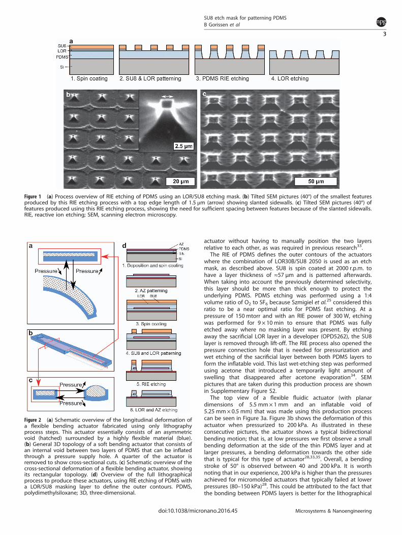
RESULTS AND DISCUSSIONReactive ion etching of PDMSTo determine the opportunities and limitations of the processabove, we first processed a range of pillars with differentdimensions and spacing in order to establish the minimal featuresize that can be achieved by this process. For this, a thin PDMSlayer (Sylgard 184, 10:1) is spin coated at 6000 r.p.m. (5 μm) and iscoated by an etch mask consisting of a layer of LOR1A spin coatedat 1000 r.p.m. (0.2 μm) and a layer of SU82002 spin coatedat 2000 r.p.m. (2.4 μm). The latter is patterned by ultravioletlithography to define pillars with a square cross section. Etchingparameters were 1:4 of O2:SF6 at a pressure of 150 mtorr, total gasflow rate of 95 sscm and an RIE power of 300 W, for 2 × 10 min.Figure 1b shows an SEM picture of the smallest features achievedunder these test conditions. These pillars have a top edge lengthof 1.5 μm, increasing in cross section towards the base. Theseslanted sidewalls have also been reported by Szmigiel et al.25 andcan be made steeper by lowering the etching pressure at the costof slower etch rates. These sloped edges also limit the minimalspacing of features, as illustrated in Figure 1c, where a spacing of20 μm was required to create separated PDMS structures.Improvements in the aspect ratio of the structures will be neededfor applications requiring closely spaced PDMS features.Our etching experiments showed a PDMS etch rate of
51 μm h− 1 and an SU8 etch rate of 15 μm h− 1, resulting in aprocess selectivity of 3.4. Specifically, SU8 masks should be aboutone-third the thickness of the PDMS layer to provide a sufficientetch barrier while retaining good resolution. Finally, our processresulted in clean top surfaces in contrast to previous publica-tions11,21,23 and our own experiments using metal hard masksin the same etcher, as shown in Supplementary Figure S1. Thisfigure compares top surfaces using aluminum hard masks(Supplementary Figure S1a) to LOR-SU8 masks on a thick PDMSlayer (Supplementary Figure S1b).
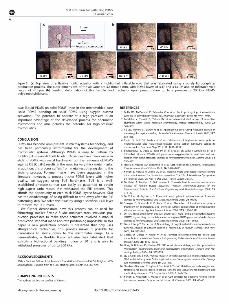
Soft microactuator demonstratorTo demonstrate the opportunities offered by this etchingtechnology, a lithography production process was developed forfabricating flexible fluidic actuators. These actuators use fluidpressure to inflate closed volumes that cause a highly elasticsurrounding structure to deform. Previous research has shownthat bending28, twisting29, and elongation or contraction30 can beachieved by these actuators. Because of their compliancy, theseactuators can be used to handle delicate objects or can beused in surgical operations31. The actuator described in this paperexhibits a large bending deformation when pressurized. Thisdeformation is achieved by inflating a void between two layers ofPDMS with different thicknesses as depicted schematically inFigures 2a–c; this principle has been extensively discussed in theliterature28,32.Here we focus on a new production flow for these actuators
(Figure 2d). First, a 70-nm TiN layer is deposited to prevent PDMSfrom sticking to the Si wafer and to ease the removal of theactuators at the end of the process. A first layer of PDMS (Sylgard184, 10:1) is spin coated at 3000 r.p.m., resulting in a layerthickness of ≈37 μm. Then, a sacrificial layer is deposited andpatterned to create the internal channels and voids according tothe actuator design. The material used for this sacrificial layer is AZ4562 (MicroChem); then, the material is spin coated at 2000 r.p.m.and patterned to form a rectangular void with a thickness of≈10 μm. To seal the void, another layer of PDMS was spin coatedat a speed of 6000 r.p.m., resulting in an average thickness of≈23 μm, leading to a local layer thickness on top of the sacrificialstructure of ≈13 μm. The thickness ratio of the PDMS layers waschosen in the range of 2 to 3, because this range leads to optimalactuation performance28. The combination of the two previoussteps makes it possible to define the inner structures of the
Table 1 Literature overview of RIE of PDMS
RIE gasses Gas ratio Etch rate (μm h− 1) Mask
SF6 —, Vlachopoulou23 48 Aluminum
CF4:O2 3:1, Garra12 20 Aluminum
1:1, Oh11 60 AZ9260
SF6:O2 4:1, Bjørnsen24 30 Glass slide
3:1, Szmigiel25 72 Aluminum
He:SF6 95:5, Tserepi26 72 AZ5214
Abbreviations: PDMS, polydimethylsiloxane; RIE, reactive ion etching.
SU8 etch mask for patterning PDMSB Gorissen et al
2
Microsystems & Nanoengineering doi:10.1038/micronano.2016.45
actuator without having to manually position the two layersrelative to each other, as was required in previous research33.The RIE of PDMS defines the outer contours of the actuators
where the combination of LOR30B/SU8 2050 is used as an etchmask, as described above. SU8 is spin coated at 2000 r.p.m. tohave a layer thickness of ≈57 μm and is patterned afterwards.When taking into account the previously determined selectivity,this layer should be more than thick enough to protect theunderlying PDMS. PDMS etching was performed using a 1:4volume ratio of O2 to SF6 because Szmigiel et al.25 considered thisratio to be a near optimal ratio for PDMS fast etching. At apressure of 150 mtorr and with an RIE power of 300 W, etchingwas performed for 9 × 10 min to ensure that PDMS was fullyetched away where no masking layer was present. By etchingaway the sacrificial LOR layer in a developer (OPD5262), the SU8layer is removed through lift-off. The RIE process also opened thepressure connection hole that is needed for pressurization andwet etching of the sacrificial layer between both PDMS layers toform the inflatable void. This last wet-etching step was performedusing acetone that introduced a temporarily light amount ofswelling that disappeared after acetone evaporation34. SEMpictures that are taken during this production process are shownin Supplementary Figure S2.The top view of a flexible fluidic actuator (with planar
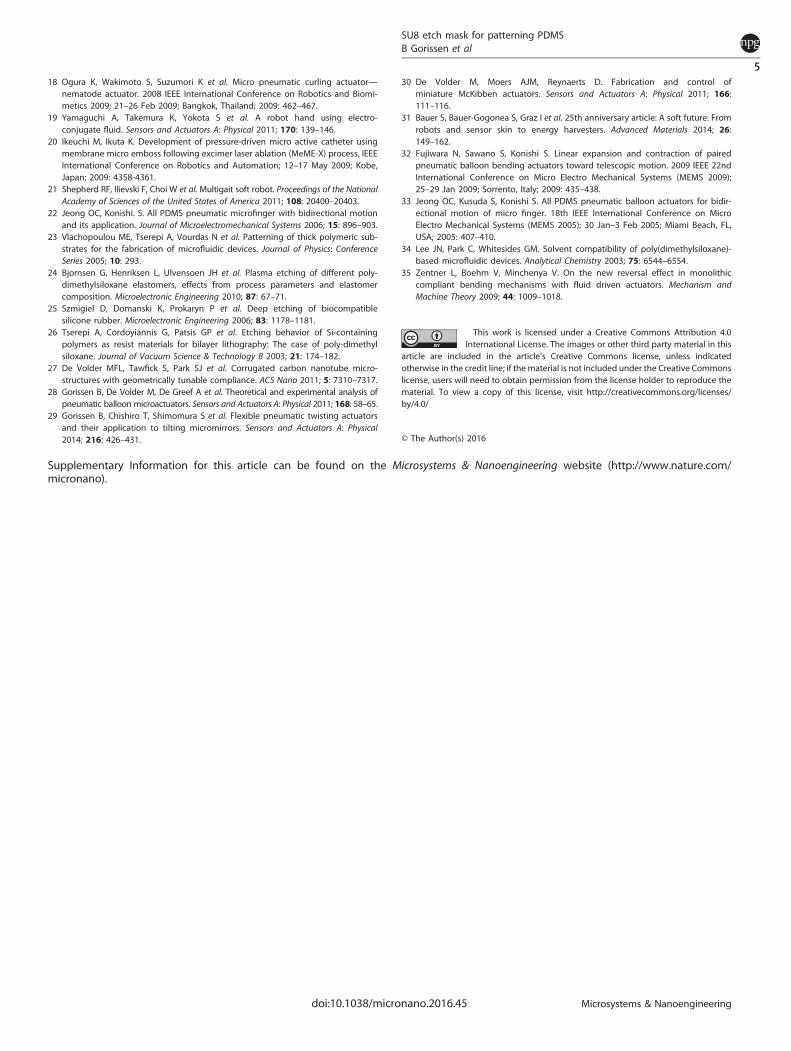
dimensions of 5.5 mm×1 mm and an inflatable void of5.25 mm×0.5 mm) that was made using this production processcan be seen in Figure 3a. Figure 3b shows the deformation of thisactuator when pressurized to 200 kPa. As illustrated in theseconsecutive pictures, the actuator shows a typical bidirectionalbending motion; that is, at low pressures we first observe a smallbending deformation at the side of the thin PDMS layer and atlarger pressures, a bending deformation towards the other sidethat is typical for this type of actuator28,33,35. Overall, a bendingstroke of 50° is observed between 40 and 200 kPa. It is worthnoting that in our experience, 200 kPa is higher than the pressuresachieved for micromolded actuators that typically failed at lowerpressures (80–150 kPa)28. This could be attributed to the fact thatthe bonding between PDMS layers is better for the lithographical
Figure 1 (a) Process overview of RIE etching of PDMS using an LOR/SU8 etching mask. (b) Tilted SEM pictures (40°) of the smallest featuresproduced by this RIE etching process with a top edge length of 1.5 μm (arrow) showing slanted sidewalls. (c) Tilted SEM pictures (40°) offeatures produced using this RIE etching process, showing the need for sufficient spacing between features because of the slanted sidewalls.RIE, reactive ion etching; SEM, scanning electron microscopy.
Figure 2 (a) Schematic overview of the longitudinal deformation ofa flexible bending actuator fabricated using only lithographyprocess steps. This actuator essentially consists of an asymmetricvoid (hatched) surrounded by a highly flexible material (blue).(b) General 3D topology of a soft bending actuator that consists ofan internal void between two layers of PDMS that can be inflatedthrough a pressure supply hole. A quarter of the actuator isremoved to show cross-sectional cuts. (c) Schematic overview of thecross-sectional deformation of a flexible bending actuator, showingits rectangular topology. (d) Overview of the full lithographicalprocess to produce these actuators, using RIE etching of PDMS witha LOR/SU8 masking layer to define the outer contours. PDMS,polydimethylsiloxane; 3D, three-dimensional.
SU8 etch mask for patterning PDMSB Gorissen et al
3
Microsystems & Nanoengineeringdoi:10.1038/micronano.2016.45
case (liquid PDMS on solid PDMS) than in the micromolded case(solid PDMS bonding on solid PDMS using oxygen plasmaactivation). The potential to operate at a high pressure is animportant advantage of the developed process for pneumaticmicrorobots and also includes the potential for high-pressuremicrofluidics.
CONCLUSIONPDMS has become omnipresent in microsystems technology andhas been particularly instrumental for the development ofmicrofluidic systems. Although PDMS is easy to pattern bymolding, it is very difficult to etch. Advances have been made inetching PDMS with metal hardmasks, but the resilience of PDMSagainst RIE (O2:SF6) results in the need for very thick metal masks.In addition, this process suffers from metal resputtering during theetching process. Polymer masks have been suggested in theliterature; however, to process thicker PDMS layers with higherquality, we suggest using SU8 hardmasks. SU8 is a well-established photoresist that can easily be patterned to obtainhigh aspect ratio masks that withstand the RIE process. Thisaffords the opportunity to etch thick PDMS layers; however, SU8has the disadvantage of being difficult to strip away after the RIEpatterning step. We solve this issue by using a sacrificial LOR layerto remove the SU8 mask.We further demonstrate how this process can be used for
fabricating smaller flexible fluidic microactuators. Previous pro-duction processes to make these actuators involved a manualproduction step that made accurate positioning impossible. In thispaper, a new production process is presented that only useslithographical techniques; this process makes it possible fordimensions to shrink down to the micrometer range. As ademonstrator, a flexible fluidic actuator was fabricated thatexhibits a bidirectional bending motion of 50° and is able towithstand pressures of up to 200 kPa.
ACKNOWLEDGEMENTSBG is a Doctoral Fellow of the Research Foundation—Flanders (F.W.O.), Belgium. MDVacknowledges support from the ERC starting grant HIENA (no. 337739).
COMPETING INTERESTSThe authors declare no conflict of interest.
REFERENCES1 Duffy DC, McDonald JC, Schueller OJA et al. Rapid prototyping of microfluidic
systems in poly(dimethylsiloxane). Analytical Chemistry 1998; 70: 4974–4984.2 Rondelez Y, Tresset G, Tabata KV et al. Microfabricated arrays of femtoliter
chambers allow single molecule enzymology. Nature Biotechnology 2005; 23:361–365.
3 Xu QB, Mayers BT, Lahav M et al. Approaching zero: Using fractured crystals inmetrology for replica molding. Journal of the American Chemical Society 2005; 127:854–855.
4 Copic D, Park SJ, Tawfick S et al. Fabrication of high-aspect-ratio polymermicrostructures and hierarchical textures using carbon nanotube compositemaster molds. Lab on a Chip 2011; 11: 1831–1837.
5 Bhattacharya S, Datta A, Berg JM et al. Studies on surface wettability of poly(dimethyl) siloxane (PDMS) and glass under oxygen-plasma treatment and cor-relation with bond strength. Journal of Microelectromechanical Systems 2005; 14:590–597.
6 Ilievski F, Mazzeo AD, Shepherd RE et al. Soft Robotics for Chemists. AngewandteChemie: International Edition 2011; 50: 1890–1895.
7 Konishi S, Nokata M, Jeong OC et al. Merging micro and macro robotics towardmicro manipulation for biomedical operation. The 36th International Symposiumon Robotics 2005; 29 Nov–1 Dec 2005; Tokyo, Japan; 36: 54.
8 De Greef A, Lambert P, Delchambre A. Towards flexible medical instruments:Review of flexible fluidic actuators. Precision Engineering-Journal of theInternational Societies for Precision Engineering and Nanotechnology 2009; 33:311–321.
9 De Volder M, Reynaerts D. Pneumatic and hydraulic microactuators: A review.Journal of Micromechanics and Microengineering 2010; 20: 043001.
10 Szmigiel D, Domanski K, Prokaryn P et al. The effect of fluorine-based plasmatreatment on morphology and chemical surface composition of biocompatiblesilicone elastomer. Applied Surface Science 2006; 253: 1506–1511.
11 Oh SR. Thick single-layer positive photoresist mold and poly(dimethylsiloxane)(PDMS) dry etching for the fabrication of a glass-PDMS-glass microfluidic device.Journal of Micromechanics and Microengineering 2008; 18: 115025.
12 Garra J, Long T, Currie J et al. Dry etching of polydimethylsiloxane for microfluidicsystems. Journal of Vacuum Science & Technology a-Vacuum Surfaces and Films2002; 20: 975–982.
13 Cristea D, Obreja P, Kusko M et al. Polymer micromachining for micro- andnanophotonics. Materials Science & Engineering C-Biomimetic and SupramolecularSystems 2006; 26: 1049–1055.
14 Hong G, Holmes AS, Heaton ME. SU8 resist plasma etching and its optimisation.Microsystem Technologies-Micro-and Nanosystems-Information Storage and Pro-cessing Systems 2004; 10: 357–359.
15 Liu J, Cai B, Zhu J et al. Process research of high caspect ratio microstructure usingSU-8 resist. Microsystem Technologies-Micro-and Nanosystems-Information Storageand Processing Systems 2004; 10: 265–268.
16 Shacham-Diamand Y, Krylov S, Shmilovich T et al. Metallization technologies andstrategies for plastic based biochips, sensors and actuators for healthcare andmedical applications. ECS Transactions 2009; 1: 243–254.
17 Konishi S, Kobayashi T, Maeda H et al. Cuff actuator for adaptive holding condi-tion around nerves. Sensors and Actuators B: Chemical 2002; 83: 60–66.
Figure 3 (a) Top view of a flexible fluidic actuator with a highlighted inflatable void that was fabricated using a purely lithographicalproduction process. The outer dimensions of the actuator are 5.5 mm×1 mm, with PDMS layers of ≈37 and ≈13 μm and an inflatable voidheight of ≈10 μm. (b) Bending deformation of this flexible fluidic actuator upon pressurization up to a pressure of 200 kPa. PDMS,polydimethylsiloxane.
SU8 etch mask for patterning PDMSB Gorissen et al
4
Microsystems & Nanoengineering doi:10.1038/micronano.2016.45
18 Ogura K, Wakimoto S, Suzumori K et al. Micro pneumatic curling actuator—nematode actuator. 2008 IEEE International Conference on Robotics and Biomi-metics 2009; 21–26 Feb 2009; Bangkok, Thailand; 2009: 462–467.
19 Yamaguchi A, Takemura K, Yokota S et al. A robot hand using electro-conjugate fluid. Sensors and Actuators A: Physical 2011; 170: 139–146.
20 Ikeuchi M, Ikuta K. Development of pressure-driven micro active catheter usingmembrane micro emboss following excimer laser ablation (MeME-X) process. IEEEInternational Conference on Robotics and Automation; 12–17 May 2009; Kobe,Japan; 2009: 4358-4361.
21 Shepherd RF, Ilievski F, Choi W et al.Multigait soft robot. Proceedings of the NationalAcademy of Sciences of the United States of America 2011; 108: 20400–20403.
22 Jeong OC, Konishi. S. All PDMS pneumatic microfinger with bidirectional motionand its application. Journal of Microelectromechanical Systems 2006; 15: 896–903.
23 Vlachopoulou ME, Tserepi A, Vourdas N et al. Patterning of thick polymeric sub-strates for the fabrication of microfluidic devices. Journal of Physics: ConferenceSeries 2005; 10: 293.
24 Bjornsen G, Henriksen L, Ulvensoen JH et al. Plasma etching of different poly-dimethylsiloxane elastomers, effects from process parameters and elastomercomposition. Microelectronic Engineering 2010; 87: 67–71.
25 Szmigiel D, Domanski K, Prokaryn P et al. Deep etching of biocompatiblesilicone rubber. Microelectronic Engineering 2006; 83: 1178–1181.
26 Tserepi A, Cordoyiannis G, Patsis GP et al. Etching behavior of Si-containingpolymers as resist materials for bilayer lithography: The case of poly-dimethylsiloxane. Journal of Vacuum Science & Technology B 2003; 21: 174–182.
27 De Volder MFL, Tawfick S, Park SJ et al. Corrugated carbon nanotube micro-structures with geometrically tunable compliance. ACS Nano 2011; 5: 7310–7317.
28 Gorissen B, De Volder M, De Greef A et al. Theoretical and experimental analysis ofpneumatic balloon microactuators. Sensors and Actuators A: Physical 2011; 168: 58–65.
29 Gorissen B, Chishiro T, Shimomura S et al. Flexible pneumatic twisting actuatorsand their application to tilting micromirrors. Sensors and Actuators A: Physical2014; 216: 426–431.
30 De Volder M, Moers AJM, Reynaerts D. Fabrication and control ofminiature McKibben actuators. Sensors and Actuators A: Physical 2011; 166:111–116.
31 Bauer S, Bauer-Gogonea S, Graz I et al. 25th anniversary article: A soft future: Fromrobots and sensor skin to energy harvesters. Advanced Materials 2014; 26:149–162.
32 Fujiwara N, Sawano S, Konishi S. Linear expansion and contraction of pairedpneumatic balloon bending actuators toward telescopic motion. 2009 IEEE 22ndInternational Conference on Micro Electro Mechanical Systems (MEMS 2009);25–29 Jan 2009; Sorrento, Italy; 2009: 435–438.
33 Jeong OC, Kusuda S, Konishi S. All PDMS pneumatic balloon actuators for bidir-ectional motion of micro finger. 18th IEEE International Conference on MicroElectro Mechanical Systems (MEMS 2005); 30 Jan–3 Feb 2005; Miami Beach, FL,USA; 2005: 407–410.
34 Lee JN, Park C, Whitesides GM. Solvent compatibility of poly(dimethylsiloxane)-based microfluidic devices. Analytical Chemistry 2003; 75: 6544–6554.
35 Zentner L, Boehm V, Minchenya V. On the new reversal effect in monolithiccompliant bending mechanisms with fluid driven actuators. Mechanism andMachine Theory 2009; 44: 1009–1018.
This work is licensed under a Creative Commons Attribution 4.0International License. The images or other third party material in this
article are included in the article’s Creative Commons license, unless indicatedotherwise in the credit line; if the material is not included under the Creative Commonslicense, users will need to obtain permission from the license holder to reproduce thematerial. To view a copy of this license, visit http://creativecommons.org/licenses/by/4.0/
© The Author(s) 2016
Supplementary Information for this article can be found on the Microsystems & Nanoengineering website (http://www.nature.com/micronano).
SU8 etch mask for patterning PDMSB Gorissen et al
5
Microsystems & Nanoengineeringdoi:10.1038/micronano.2016.45