Embed Size (px)
DESCRIPTION
A presentation used during the lecture for PhD students at Chulalongkorn University on 27 January 2011
Citation preview
1
Study of Surface Defects usingFocused Ion Beam (FIB) Milling andTransmission Electron Microscope (TEM) Techniques
Presented by
Sitthichoke Chaiwan B.E.(Ceramics), UNSW27 January 2011
2
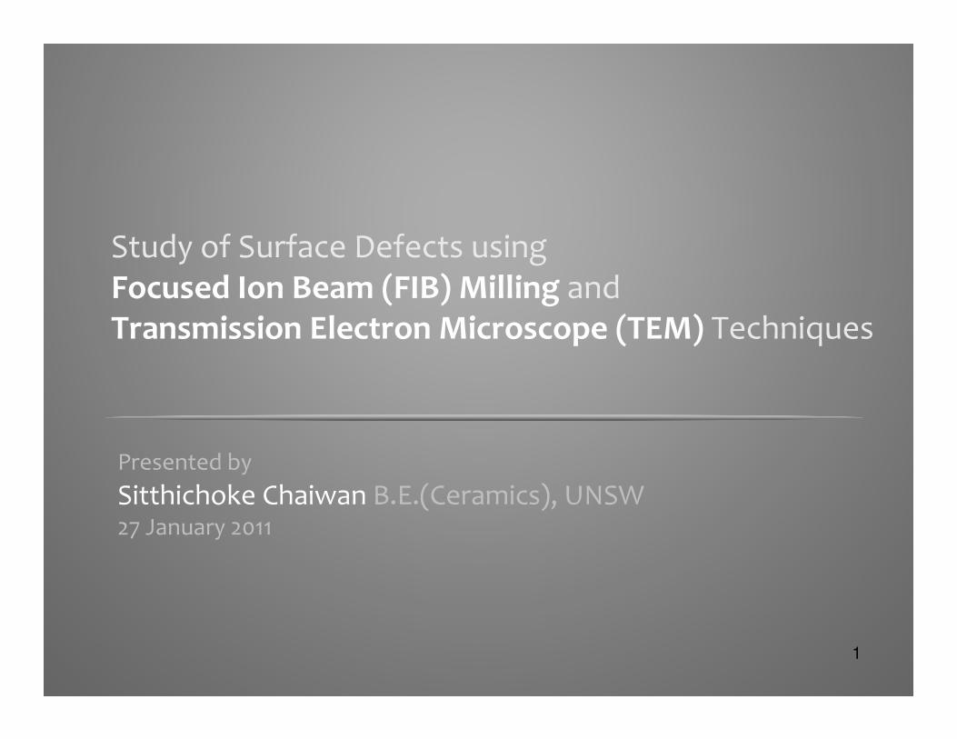
OutlinesOutlines
• Exploring inherent properties
• Characteristic and Applications of FIB milling
• Preparation of TEM samples using FIB milling
• Investigation of subsurface damage
3
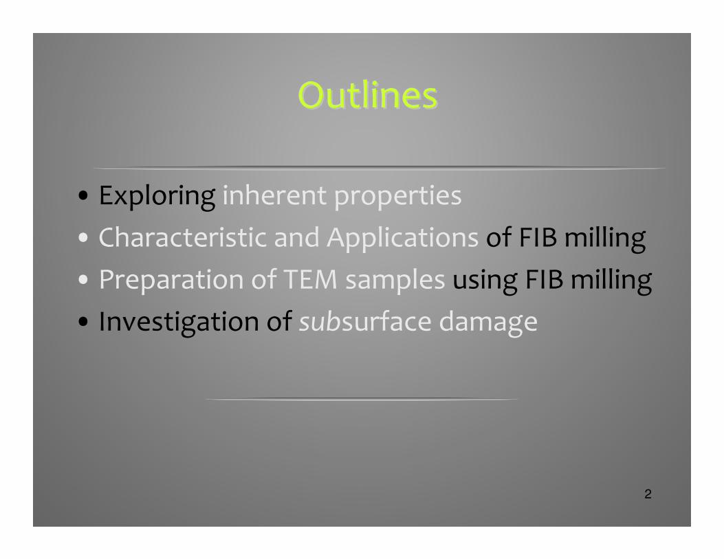
Properties of Materials
• Mechanical properties– Compressive strength
– Ductility
– Flexural strength
– Fracture toughness
– Hardness
– Poisson's ratio
– Specific modulus
– Tensile strength
– Yield strength
– Young's modulus
– Density
• Electrical properties– Dielectric constant
– Piezoelectric constants
• Thermal properties– Thermal conductivity
– Thermal expansion
– Melting point, Eutectic point
– Specific heat
• Chemical properties
– Surface energy
– Specific internal surface area
• Magnetic properties– Diamagnetism
– Hysteresis
• Other properties– Optical properties
• Reflectivity• Color• Photosensitivity
– Acoustical properties
– Radiological properties
Numbers of contributing factors for a specific
material!!
4
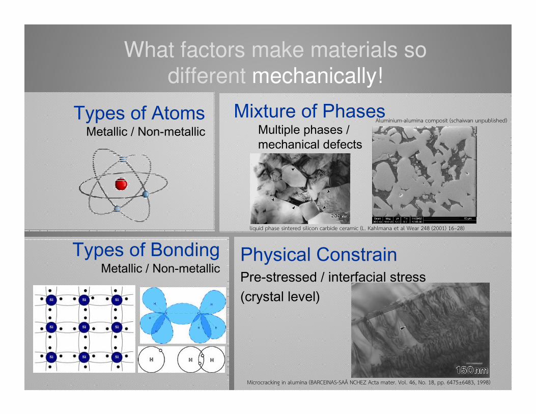
Physical ConstrainPre-stressed / interfacial stress (crystal level)
What factors make materials so different mechanically!
Mixture of PhasesMultiple phases / mechanical defects
Types of AtomsMetallic / Non-metallic
Types of BondingMetallic / Non-metallic
liquid phase sintered silicon carbide ceramic (L. Kahlmana et al Wear 248 (2001) 16–28)
Aluminium-alumina composit (schaiwan unpublished)
Microcracking in alumina (BARCEINAS-SAÂ NCHEZ Acta mater. Vol. 46, No. 18, pp. 6475±6483, 1998)
5
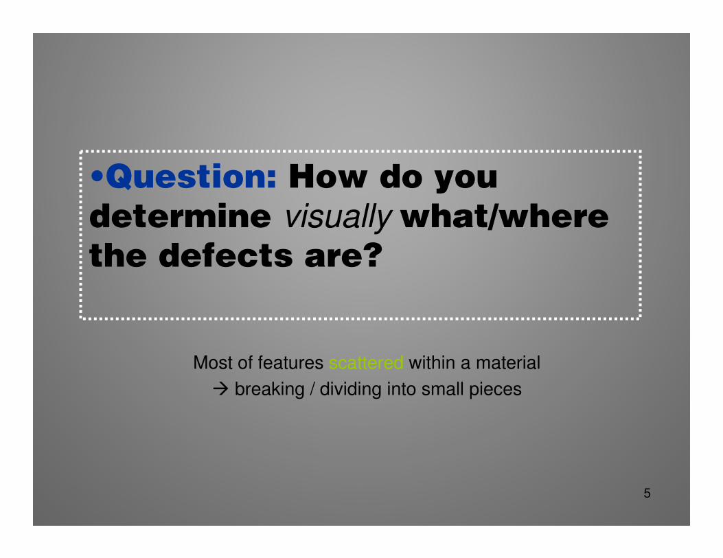
Most of features scattered within a material
� breaking / dividing into small pieces
•Question: How do you
determine visually what/where
the defects are?
6
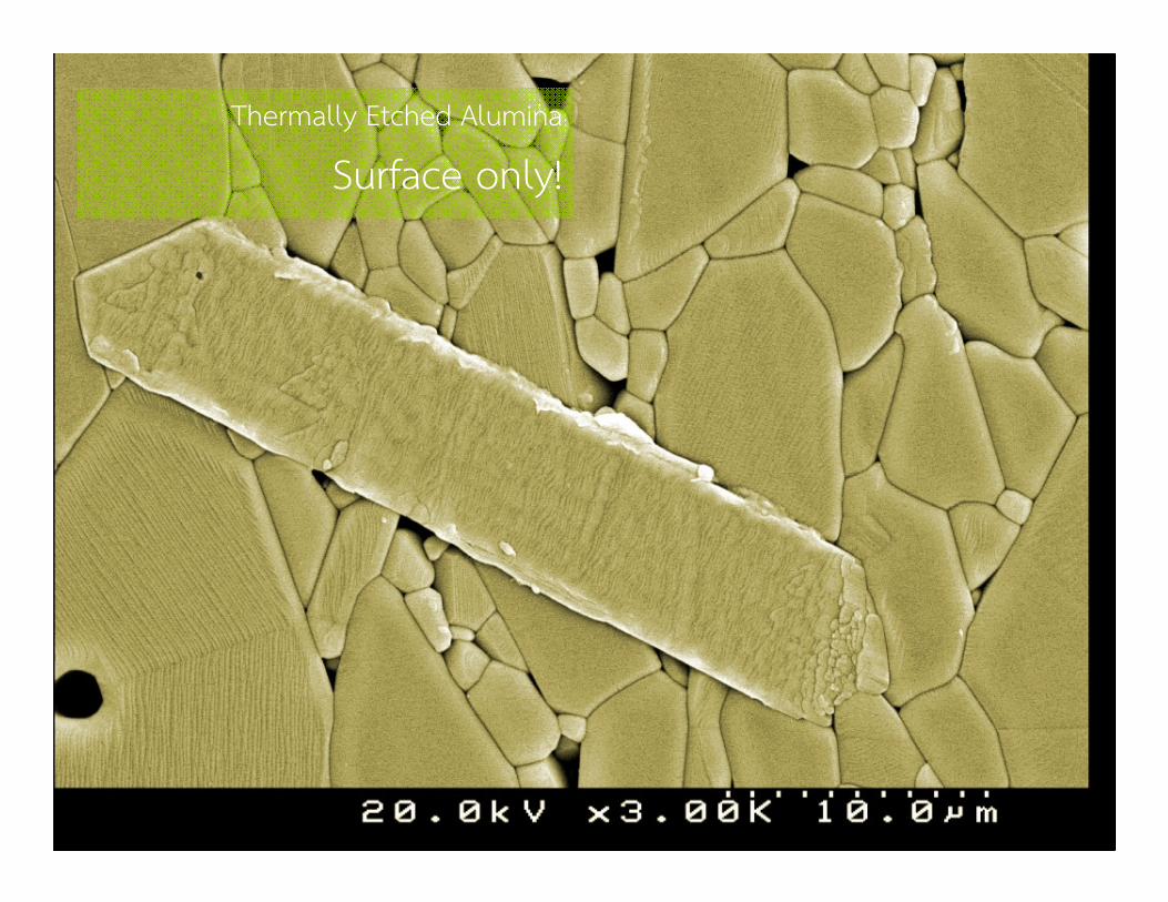
Thermally Etched Alumina
Surface only!
7
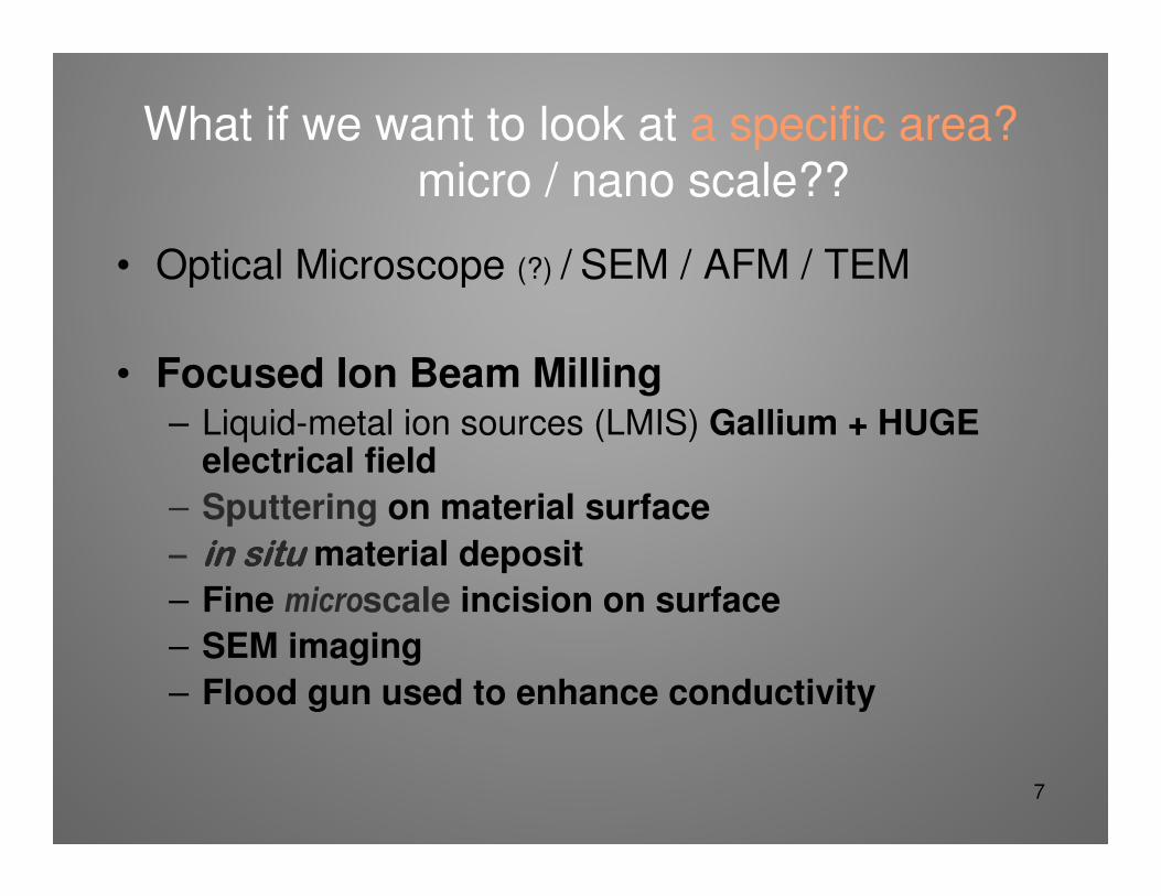
What if we want to look at a specific area?micro / nano scale??
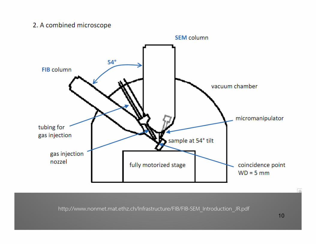
• Optical Microscope (?) / SEM / AFM / TEM
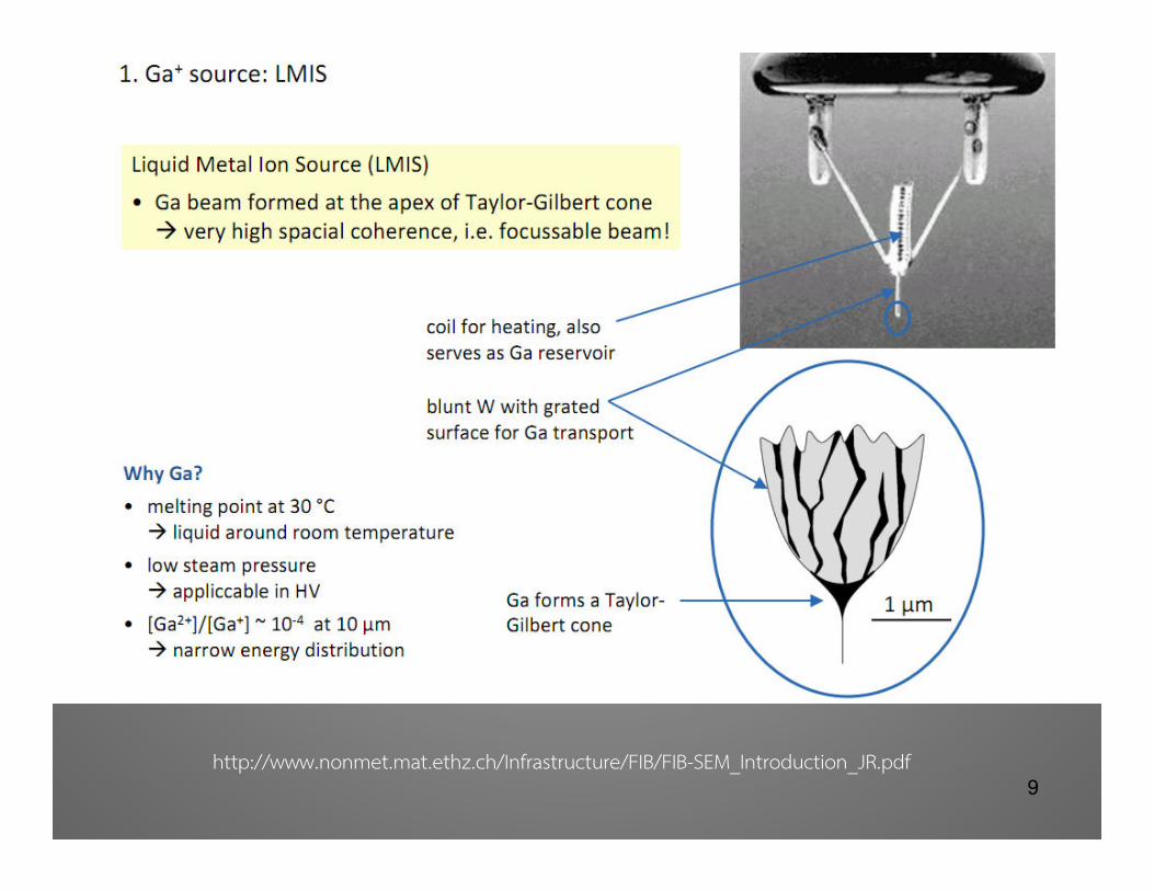
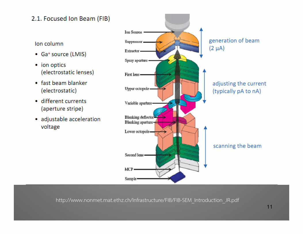
• Focused Ion Beam Milling– Liquid-metal ion sources (LMIS) Gallium + HUGE
electrical field
– Sputtering on material surface
– in situin situin situin situ material deposit
– Fine microscale incision on surface
– SEM imaging
– Flood gun used to enhance conductivity
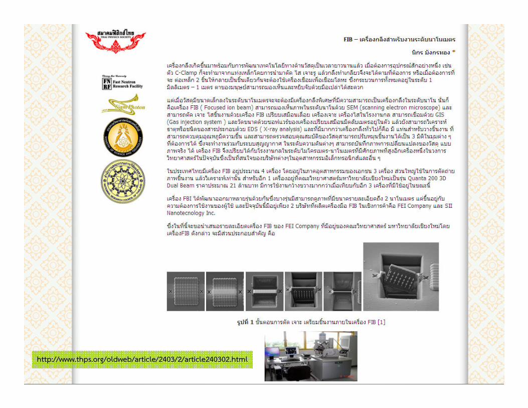
8http://www.thps.org/oldweb/article/2403/2/article240302.html
9
http://www.nonmet.mat.ethz.ch/Infrastructure/FIB/FIB-SEM_Introduction_JR.pdf
10
http://www.nonmet.mat.ethz.ch/Infrastructure/FIB/FIB-SEM_Introduction_JR.pdf
11
http://www.nonmet.mat.ethz.ch/Infrastructure/FIB/FIB-SEM_Introduction_JR.pdf
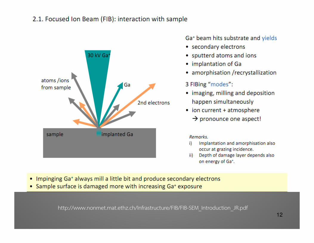
12
http://www.nonmet.mat.ethz.ch/Infrastructure/FIB/FIB-SEM_Introduction_JR.pdf
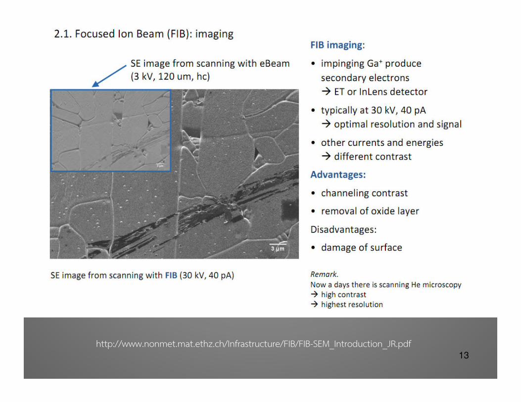
13
http://www.nonmet.mat.ethz.ch/Infrastructure/FIB/FIB-SEM_Introduction_JR.pdf
14
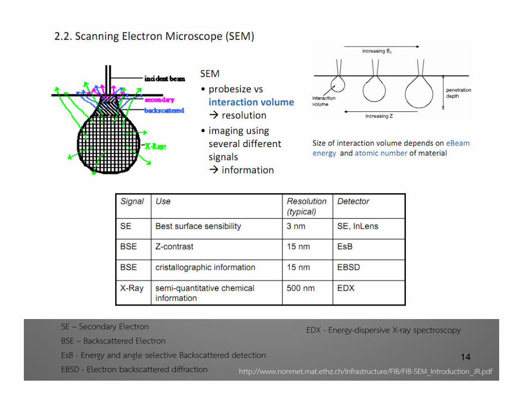
SE – Secondary ElectronBSE – Backscattered Electron EsB - Energy and angle selective Backscattered detectionEBSD - Electron backscattered diffraction
EDX - Energy-dispersive X-ray spectroscopy
http://www.nonmet.mat.ethz.ch/Infrastructure/FIB/FIB-SEM_Introduction_JR.pdf
15
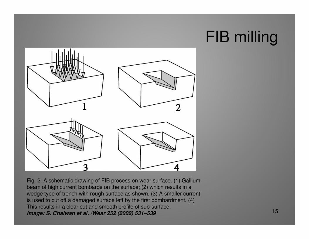
FIB milling
Fig. 2. A schematic drawing of FIB process on wear surface. (1) Galliumbeam of high current bombards on the surface; (2) which results in awedge type of trench with rough surface as shown. (3) A smaller currentis used to cut off a damaged surface left by the first bombardment. (4)This results in a clear cut and smooth profile of sub-surface.Image: S. Chaiwan et al. /Wear 252 (2002) 531–539
16
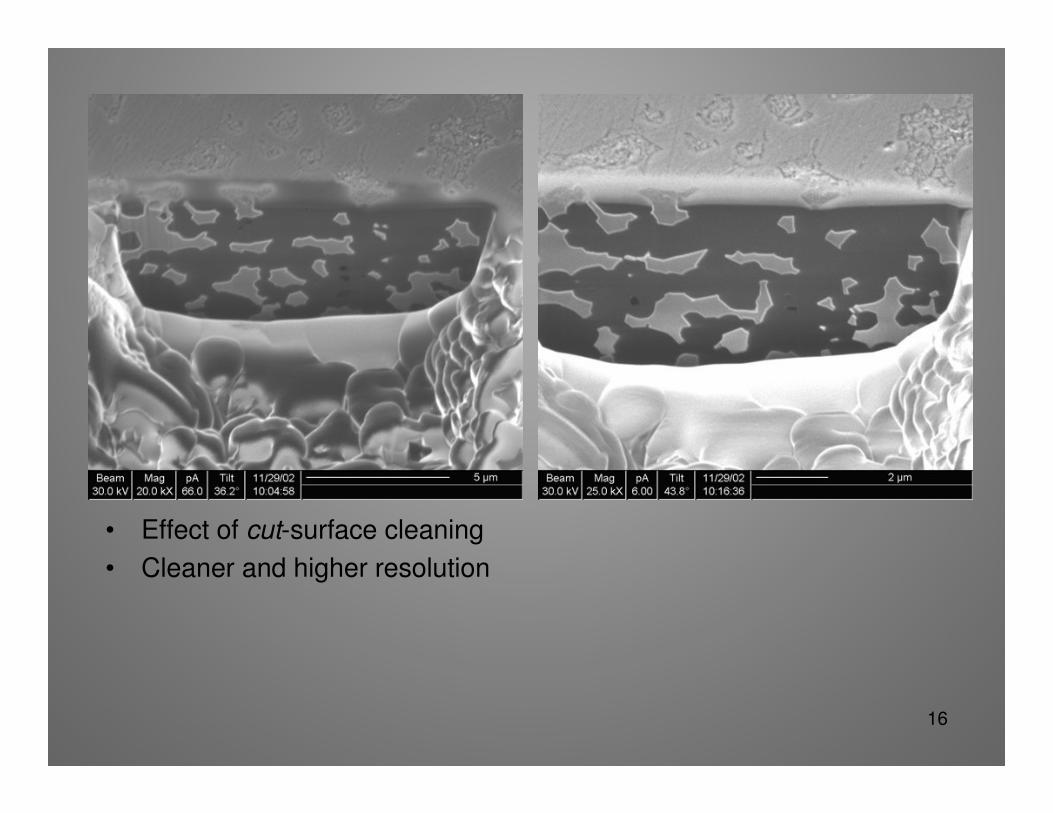
• Effect of cut-surface cleaning
• Cleaner and higher resolution
17
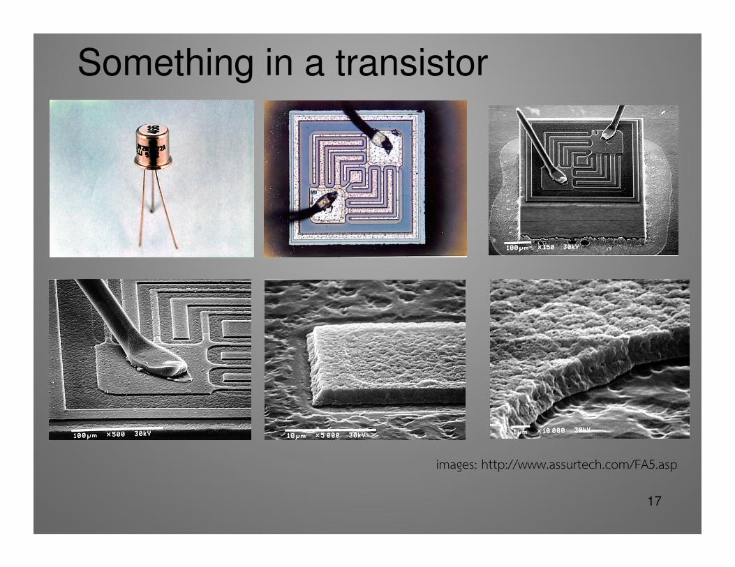
Something in a transistor
images: http://www.assurtech.com/FA5.asp
18
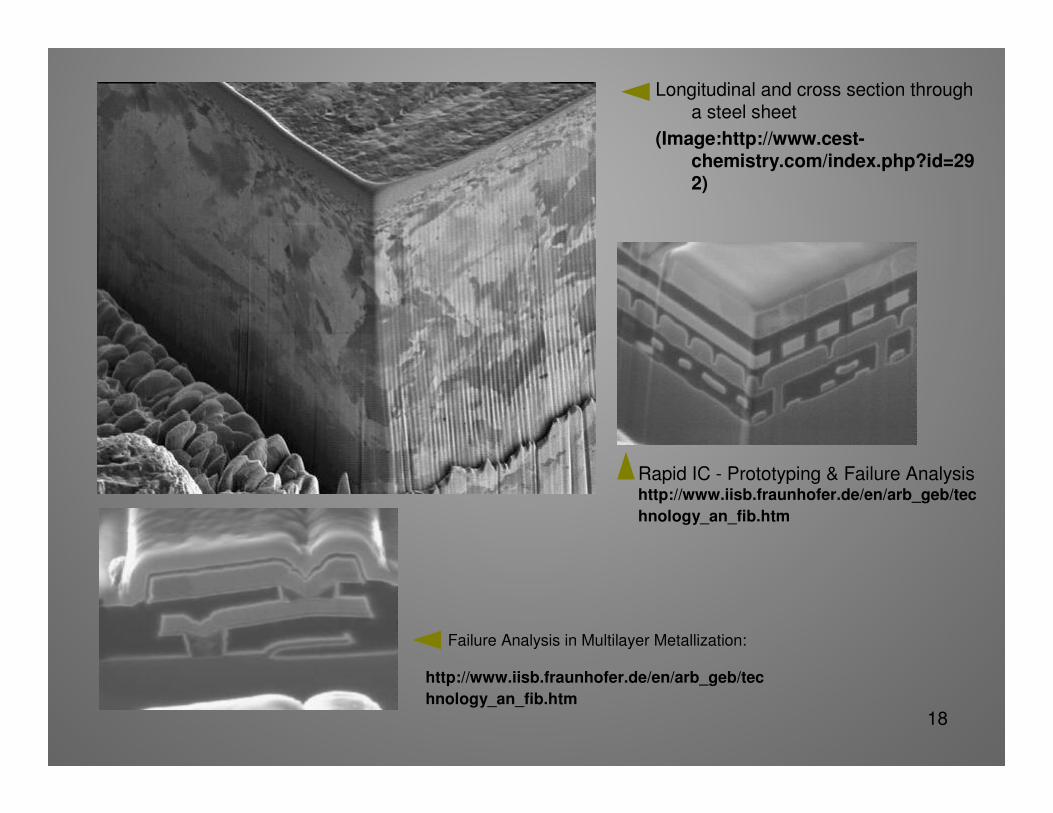
Longitudinal and cross section through a steel sheet
(Image:http://www.cest-chemistry.com/index.php?id=292)
Rapid IC - Prototyping & Failure Analysishttp://www.iisb.fraunhofer.de/en/arb_geb/tec
hnology_an_fib.htm
Failure Analysis in Multilayer Metallization:
http://www.iisb.fraunhofer.de/en/arb_geb/tec
hnology_an_fib.htm
19
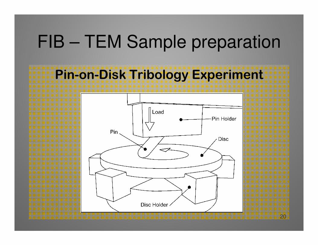
20
Pin-on-Disk Tribology Experiment
FIB – TEM Sample preparation
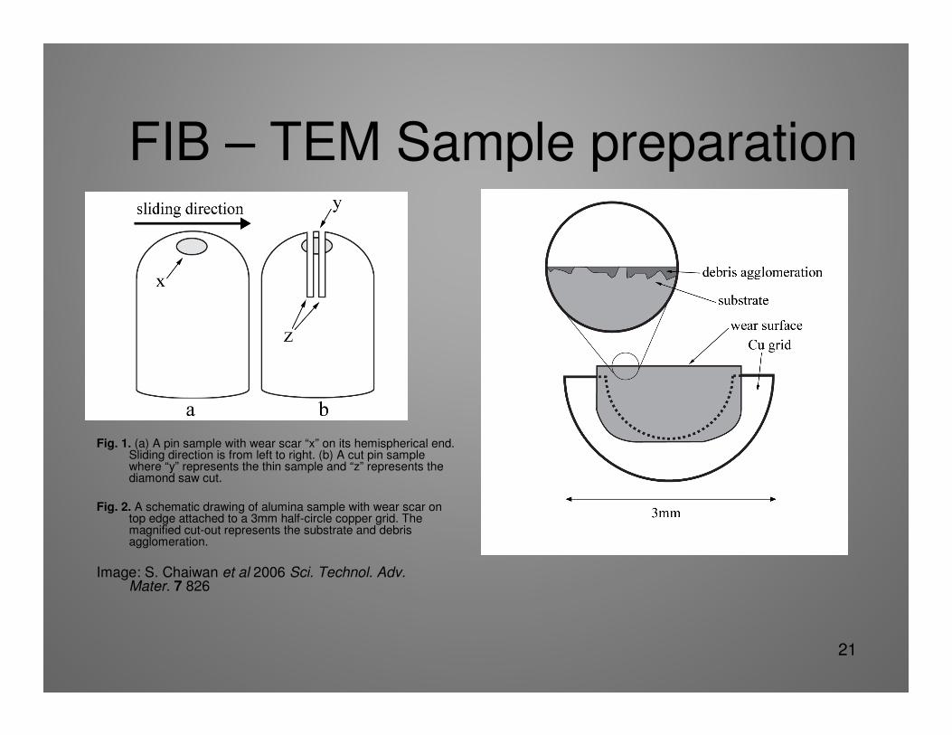
21
Fig. 1. (a) A pin sample with wear scar “x” on its hemispherical end. Sliding direction is from left to right. (b) A cut pin sample where “y” represents the thin sample and “z” represents the diamond saw cut.
Fig. 2. A schematic drawing of alumina sample with wear scar on top edge attached to a 3mm half-circle copper grid. The magnified cut-out represents the substrate and debris agglomeration.
Image: S. Chaiwan et al 2006 Sci. Technol. Adv. Mater. 7 826
FIB – TEM Sample preparation
22
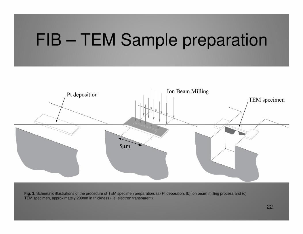
FIB – TEM Sample preparation
Fig. 3. Schematic illustrations of the procedure of TEM specimen preparation. (a) Pt deposition, (b) ion beam milling process and (c)
TEM specimen, approximately 200nm in thickness (i.e. electron transparent)
23
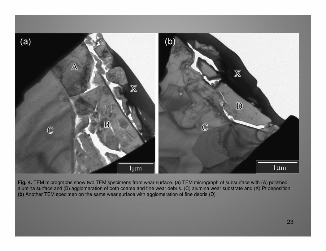
Fig. 4. TEM micrographs show two TEM specimens from wear surface. (a) TEM micrograph of subsurface with (A) polished
alumina surface and (B) agglomeration of both coarse and fine wear debris. (C) alumina wear substrate and (X) Pt deposition.
(b) Another TEM specimen on the same wear surface with agglomeration of fine debris (D)
24
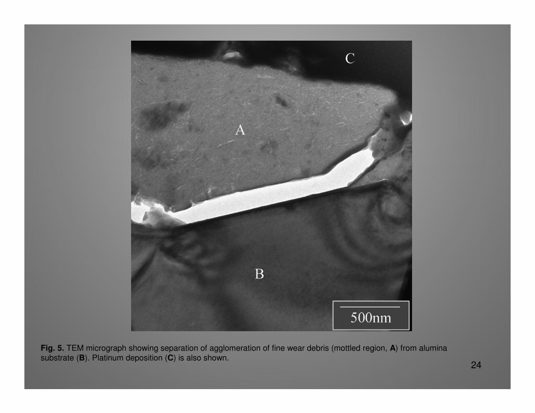
Fig. 5. TEM micrograph showing separation of agglomeration of fine wear debris (mottled region, A) from alumina
substrate (B). Platinum deposition (C) is also shown.
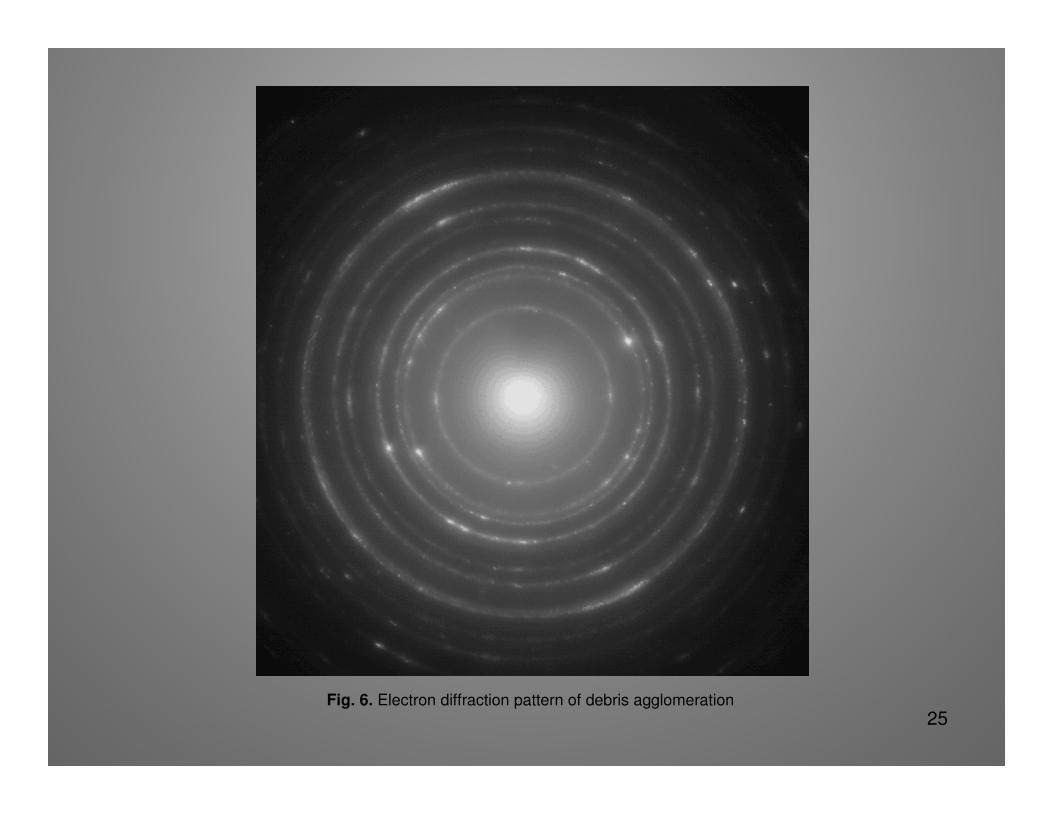
25Fig. 6. Electron diffraction pattern of debris agglomeration
26
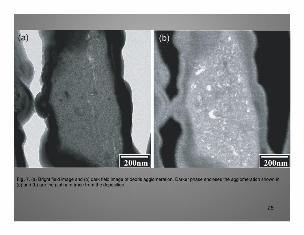
Fig. 7. (a) Bright field image and (b) dark field image of debris agglomeration. Darker phase encloses the agglomeration shown in (a) and (b) are the platinum trace from the deposition.
27
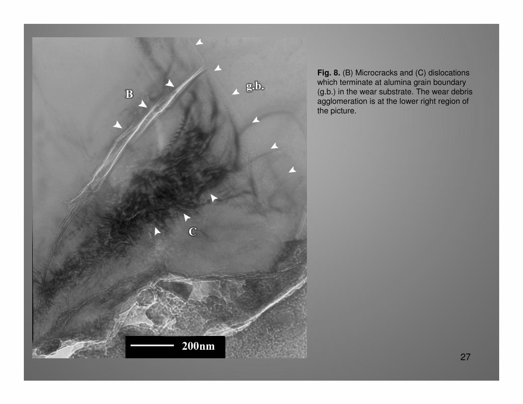
Fig. 8. (B) Microcracks and (C) dislocations
which terminate at alumina grain boundary (g.b.) in the wear substrate. The wear debris
agglomeration is at the lower right region of
the picture.

28
But….
It was near 10 years ago….
Recently there’s some evolution.

29
Video presentation


![RUNNING TIME ANALYSIS - GitHub Pages · Running time analysis of the iterative algorithm function F(n) Create an array fib[1..n] fib[1] = 1 fib[2] = 1 for i = 3 to n: fib[i] = fib[i-1]](https://img.pdfslide.us/doc/110x75/5e95ef9e965d8c2b7e7f1cbb/running-time-analysis-github-pages-running-time-analysis-of-the-iterative-algorithm.jpg)