Embed Size (px)
Citation preview
Journal of Physical Science and Application 5 (2) (2015) 128-142 doi: 10.17265/2159-5348/2015.02.007
Study of Plasma and Ion Beam Sputtering Processes
M.M.Abdelrahman Accelerators and Ion Sources Department, Nuclear Research Center, Atomic Energy Authority, 13759 Inchas, Atomic Energy, Cairo,
Egypt
Abstract: The effects of plasma (ions, electrons) and other energetic particles are now widely used for substrate cleaning as well as to assist and control thin film growth and various applications. In this work, historical review of the plasma and its various types are given and described. Different types of gas discharge and plasma production are also discussed in detail. Furthermore, technique of ion beam extraction from a plasma source for sputtering process by using a suitable electrode is carefully studied and given. In further consequence, a general review about the physics and mechanism of sputtering processes is studied. Different types of sputtering techniques are investigated and clarified. Theoretical treatment for determination of sputtering yield for low and high atomic species elements as a function of energy from 100 to 5,000 eV are studied and discussed. Finally, various applications of plasma-and-ion beam sputtering will also be mentioned and discussed. Key words: Plasma, ion sputtering, gas mixing, electron injection.
1. Introduction
The plasma is the fourth state of the matter, following the solid, liquid and gaseous states. As the temperature of the substance increased, the material changes firstly from solid to liquid, then liquid to gas and finally from gas to plasma [1]. In general, there are three different kinds of these individual particles that make up the plasma, they are ions, electrons and neutral particles. Plasma exists in nature as in the sun, stars and in the ionosphere and on the earth in transient forms such as lighting. Man made plasmas such as fluorescent lamps, neon signs and high voltage sparks industrially, plasmas are used in various forms as in semi-conductor processing, material modifications and synthesis and other purposes. The development of PS (plasma sources) received a strong push from plasma centers all over the world, due to the fact that the advancement range of these sources is strongly increased by the charge state of the plasma sources. Moreover, the plasma sources are useful for basic investigations in atomic physics, surface physics and related areas. The low energy atomic physics with
Corresponding author: M.M.Abdelrahman. E-mail:
multicharged ions was given a strong input by studies in connection with fusion research, to deepen our fundamental understanding of the mechanisms of the involved collision processes. Accurate knowledge of total electron capture cross sections helps in explaining and solving problems in the field of fusion research, astrophysics and laboratory plasma. The more demanding the applications of the plasma sources, the more the plasma source has to be carefully designed and optimised to get optimum performance. High performance of plasma sources represents in having ionization efficiency, maximum current, high charge state, size and cost taking into account the limits of power and the radiation environment. In general, the plasma (ion) source is the main component of any accelerator, from which originates the beam of ions or electrons. Hence, its specifications should be carefully considered to adapt the expected application. In its basic operation (for ions), a gas is ionized, usually by subjecting it to an electric discharge, and the positively charged ions are extracted by acceleration towards a negative electrode at a potential of negative potential. The characteristics of the ion source determine to a great extent the performance of the accelerating system. The selection
D DAVID PUBLISHING
Study of Plasma and Ion Beam Sputtering Processes
129
of an ion source for a particular application should be made with due consideration of factors such as species and intensity capability, beam quality (emittance and brightness), ionization efficiency, reliability ,ease of operation, maintenance, and source lifetime. No truly universal source exists that will meet all applications requirements. In this work, historical review of the plasma and its various types are given and described. Different types of gas discharge and plasma production are also discussed in detail. Furthermore, technique of ion beam extraction from a plasma source for sputtering process by using a suitable electrode is carefully studied and given. In a furthermore consequence, a general review about the physics and mechanism of sputtering processes is studied. Different types of sputtering techniques are investigated and clarified. Theoretical treatment for determination of sputtering yield with low and high atomic species elements as a function of incident energy from 100 to 5000 ev are studied. Finally, various applications of plasma-and-ion beam sputtering will also be mentioned and discussed.
1.1 General Considerations on Plasma Sources
Plasma is resulted from ionization of neutral gases generally equal numbers of positive and negative charge carriers. Such plasma is characterized by quasi-neutral. When blood is cleared of its various constituents, there remains a transparent liquid which was named plasma (gely). By comparison to this definition, Irving Langmuir [2] first used this term “plasma” in 1927 and won Noble prize for this discovery. Plasmas exist in nature in those environments where the temperature is adequately high, such as in the sun, stars and in the ionosphere and on the earth in transient forms such as lighting. Man-made plasmas have become commonplace and are part of the modern world in forms such as fluorescent lamps, neon signs and high voltage sparks. Laboratory plasmas can be created in a wide variety of ways, most commonly as electrical discharges of one
kind or another. Industrially, plasmas are used in various forms for semiconductor processing, lighting, materials modification and synthesis and other purposes.
1.2 Applications of Plasma Sources
Applications of plasma sources from providing beams of hundreds of amperes for fusion, nano-amperes for microprobe trace analysis, broad beams for ion implantation, space thrusters, industrial polymerisation, food sterilisation, to medical, military and accelerator applications. PIG ion sources have found widespread applications in the injectors of the large particle accelerators used for nuclear and high-energy physics research. The Freeman ion source is widely used in the commercially available ion implantation equipment. Laser ion sources, where very high energy fluxes that can be delivered onto solid targets using a high power pulsed laser can be used to produce dense pulsed plasma with a high fraction of highly stripped ion species. In the EBIS (electron beam ion source), the ions are contained within a high-energy electron beam in a strong magnetic field and in a very high vacuum, for a sufficiently long time for very high charge state ions to be produced. This ion source is particularly suitable for particle accelerator injection, especially heavy ion synchrotrons as well as to basic atomic physics. ECR ion sources have the advantage for using as high charge state ion injectors for nuclear physics, particle accelerators especially cyclotrons. Microwave ion sources used for the filamentless production of high current beams for high dose ion implantation into semiconductors. The excellent performance of the Freeman ion source is the ion implantation and industrial applications, especially for semiconductor purposes. Penning ion sources are found to be more successful than other sources for many types of accelerators. RF ion sources have been used in plasma and reactive ion beam etching and ion beam doping. Also, they are widely employed by the semiconductor
Study of Plasma and Ion Beam Sputtering Processes
130
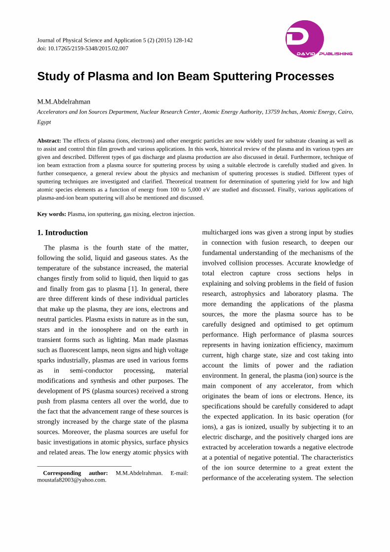
industry. Today, ion sources are considered the main component of the particle accelerator system. Particle accelerators are widely used in nearly every field of physics from elementary particles to solid state physics. They also considered an essential part in many other areas of researches as chemistry, biology, etc (Fig. 1) [3]. Industrial applications cover a wide range as ion implantation in the semiconductor industry, indeed, the modification of surface properties of many materials. Applications of accelerators in medicine have found wide areas as isotope production in view diagnostics or treatment, or for therapy with gamma rays and more recently, with neutrons and heavy charged particles.
1.3 Main Parameters of Plasma Sources
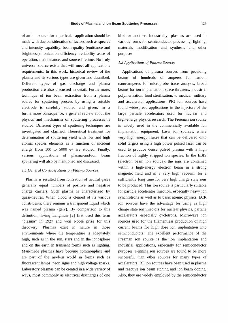
Different applications of plasma sources require somewhat different sets of certain performance characteristics. Ion sources are characterized by the following parameters [4]:
(1) The type of ion species that can be produced by the source.
(2) The ability of producing ions of different elements for their applications in particle accelerators, atomic physics, etc.
(3) The extracted ion current. (4) The beam emittance should be as low as
possible. (5) The brightness is inversely proportional to the
beam emittance, a high value is desired. (6) The energy spread of the extracted beam which
depends on the ion source parameters as the magnetic field, gas pressure and RF power (in case of RF ion sources). Ion sources with low ion energy spread is preferred.
(7) Ionization efficiency is the efficiency of the process by which the plasma is formed. A high efficiency allows high ion currents to be produced with relatively low gas flow.
(8) There are a number of other parameters that are more or less important, depending on applications as
the source lifetime, the source size, the power efficiency and the ease of maintenance. Fig. 2 illustrates the main parameters for different types of ion sources.
1.4 Gas Discharge Processes
Ionization is a process in which an atom loses one or more of its electrons to another atom. The process of ionization occurs in nature as a result of interactions of photons, electrons, or ions with matter. The most essential setup in every ionization process is
Fig. 1 The different applications of plasma sources [3].
Fig. 2 Operating parameters for different types of ion sources.
Study of Plasma and Ion Beam Sputtering Processes
131
the conversion of neutral particles into ions, electrons (plasma). In all types of ion sources, the gas ions are produced by various types of gas discharge including electron collisions with gas atoms. The general requirements are a source of electrons, a small region of relatively high gas pressure, an electric field to accelerate the electrons to produce an intense gas discharge with relatively high density plasma and finally, some mechanism for extracting a high ion current beam.
1.5 Methods of Plasma Production
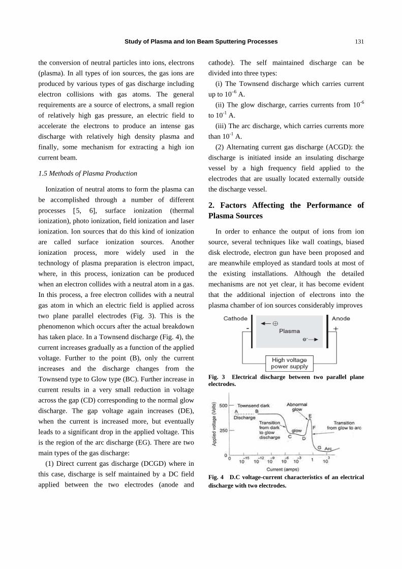
Ionization of neutral atoms to form the plasma can be accomplished through a number of different processes [5, 6], surface ionization (thermal ionization), photo ionization, field ionization and laser ionization. Ion sources that do this kind of ionization are called surface ionization sources. Another ionization process, more widely used in the technology of plasma preparation is electron impact, where, in this process, ionization can be produced when an electron collides with a neutral atom in a gas. In this process, a free electron collides with a neutral gas atom in which an electric field is applied across two plane parallel electrodes (Fig. 3). This is the phenomenon which occurs after the actual breakdown has taken place. In a Townsend discharge (Fig. 4), the current increases gradually as a function of the applied voltage. Further to the point (B), only the current increases and the discharge changes from the Townsend type to Glow type (BC). Further increase in current results in a very small reduction in voltage across the gap (CD) corresponding to the normal glow discharge. The gap voltage again increases (DE), when the current is increased more, but eventually leads to a significant drop in the applied voltage. This is the region of the arc discharge (EG). There are two main types of the gas discharge:
(1) Direct current gas discharge (DCGD) where in this case, discharge is self maintained by a DC field applied between the two electrodes (anode and
cathode). The self maintained discharge can be divided into three types:
(i) The Townsend discharge which carries current up to 10–6 A.
(ii) The glow discharge, carries currents from 10-6 to 10-1 A.
(iii) The arc discharge, which carries currents more than 10-1 A.
(2) Alternating current gas discharge (ACGD): the discharge is initiated inside an insulating discharge vessel by a high frequency field applied to the electrodes that are usually located externally outside the discharge vessel.
2. Factors Affecting the Performance of Plasma Sources
In order to enhance the output of ions from ion source, several techniques like wall coatings, biased disk electrode, electron gun have been proposed and are meanwhile employed as standard tools at most of the existing installations. Although the detailed mechanisms are not yet clear, it has become evident that the additional injection of electrons into the plasma chamber of ion sources considerably improves
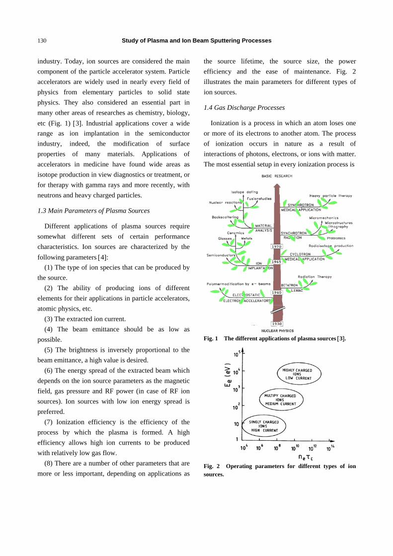
Fig. 3 Electrical discharge between two parallel plane electrodes.
Fig. 4 D.C voltage-current characteristics of an electrical discharge with two electrodes.
Study of Plasma and Ion Beam Sputtering Processes
132
its performance. Depending on the special conditions of the source, these additional electrons can both compensate for losses of plasma electrons or even may change global plasma parameters (e.g. plasma potential, electron density) and hence positively influence the extraction at high rates of ions.
2.1 Ion Cooling by Gas Mixing
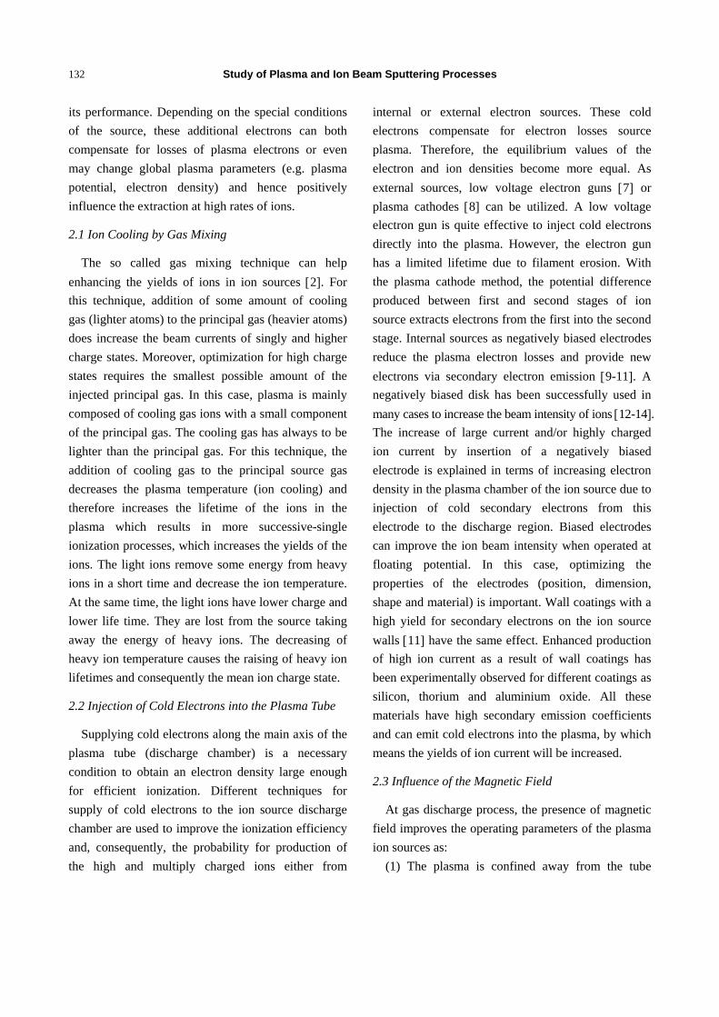
The so called gas mixing technique can help enhancing the yields of ions in ion sources [2]. For this technique, addition of some amount of cooling gas (lighter atoms) to the principal gas (heavier atoms) does increase the beam currents of singly and higher charge states. Moreover, optimization for high charge states requires the smallest possible amount of the injected principal gas. In this case, plasma is mainly composed of cooling gas ions with a small component of the principal gas. The cooling gas has always to be lighter than the principal gas. For this technique, the addition of cooling gas to the principal source gas decreases the plasma temperature (ion cooling) and therefore increases the lifetime of the ions in the plasma which results in more successive-single ionization processes, which increases the yields of the ions. The light ions remove some energy from heavy ions in a short time and decrease the ion temperature. At the same time, the light ions have lower charge and lower life time. They are lost from the source taking away the energy of heavy ions. The decreasing of heavy ion temperature causes the raising of heavy ion lifetimes and consequently the mean ion charge state.
2.2 Injection of Cold Electrons into the Plasma Tube
Supplying cold electrons along the main axis of the plasma tube (discharge chamber) is a necessary condition to obtain an electron density large enough for efficient ionization. Different techniques for supply of cold electrons to the ion source discharge chamber are used to improve the ionization efficiency and, consequently, the probability for production of the high and multiply charged ions either from
internal or external electron sources. These cold electrons compensate for electron losses source plasma. Therefore, the equilibrium values of the electron and ion densities become more equal. As external sources, low voltage electron guns [7] or plasma cathodes [8] can be utilized. A low voltage electron gun is quite effective to inject cold electrons directly into the plasma. However, the electron gun has a limited lifetime due to filament erosion. With the plasma cathode method, the potential difference produced between first and second stages of ion source extracts electrons from the first into the second stage. Internal sources as negatively biased electrodes reduce the plasma electron losses and provide new electrons via secondary electron emission [9-11]. A negatively biased disk has been successfully used in many cases to increase the beam intensity of ions [12-14]. The increase of large current and/or highly charged ion current by insertion of a negatively biased electrode is explained in terms of increasing electron density in the plasma chamber of the ion source due to injection of cold secondary electrons from this electrode to the discharge region. Biased electrodes can improve the ion beam intensity when operated at floating potential. In this case, optimizing the properties of the electrodes (position, dimension, shape and material) is important. Wall coatings with a high yield for secondary electrons on the ion source walls [11] have the same effect. Enhanced production of high ion current as a result of wall coatings has been experimentally observed for different coatings as silicon, thorium and aluminium oxide. All these materials have high secondary emission coefficients and can emit cold electrons into the plasma, by which means the yields of ion current will be increased.
2.3 Influence of the Magnetic Field
At gas discharge process, the presence of magnetic field improves the operating parameters of the plasma ion sources as:
(1) The plasma is confined away from the tube
Study of Plasma and Ion Beam Sputtering Processes
133
walls. The focusing effect of the magnetic field is due to the helical motion of the electrons along a trajectory of radius re related to the intensity of the magnetic field B [15]:
rB
m Vee
e=1 2
(1)
(2) The presence of both dc magnetic and electric fields inside the discharge tube enhanced the helical motion of electrons to make a constructive collisions with gas atoms and in turn, increases the lifetime of the ions which results in yields of high efficiency ion source.
(3) Decrease the diffusion losses across the magnetic field due to decrease of plasma oscillation caused by electron beam plasma interaction.
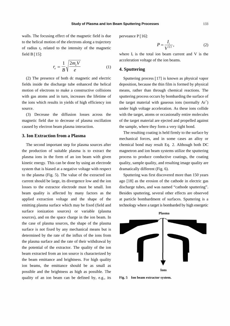
3. Ion Extraction from a Plasma
The second important step for plasma sources after the production of suitable plasma is to extract the plasma ions in the form of an ion beam with given kinetic energy. This can be done by using an electrode system that is biased at a negative voltage with respect to the plasma (Fig. 5). The value of the extracted ion current should be large, its divergence low and the ion losses to the extractor electrode must be small. Ion beam quality is affected by many factors as the applied extraction voltage and the shape of the emitting plasma surface which may be fixed (field and surface ionization sources) or variable (plasma sources), and on the space charge in the ion beam. In the case of plasma sources, the shape of the plasma surface is not fixed by any mechanical means but is determined by the rate of the influx of the ions from the plasma surface and the rate of their withdrawal by the potential of the extractor. The quality of the ion beam extracted from an ion source is characterized by the beam emittance and brightness. For high quality ion beams, the emittance should be as small as possible and the brightness as high as possible. The quality of an ion beam can be defined by, e.g., its
perveance P [16]:
3 2 ,iIPV
= (2)
where Ii is the total ion beam current and V is the acceleration voltage of the ion beams.
4. Sputtering
Sputtering process [17] is known as physical vapor deposition, because the thin film is formed by physical means, rather than through chemical reactions. The sputtering process occurs by bombarding the surface of the target material with gaseous ions (normally Ar+) under high voltage acceleration. As these ions collide with the target, atoms or occasionally entire molecules of the target material are ejected and propelled against the sample, where they form a very tight bond.
The resulting coating is held firmly to the surface by mechanical forces, and in some cases an alloy or chemical bond may result Eq. 2. Although both DC magnetron and ion beam systems utilize the sputtering process to produce conductive coatings, the coating quality, sample quality, and resulting image quality are dramatically different (Fig. 6).
Sputtering was first discovered more than 150 years ago [18] as the erosion of the cathode in electric gas discharge tubes, and was named “cathode sputtering”. Besides sputtering, several other effects are observed at particle bombardment of surfaces. Sputtering is a technology where a target is bombarded by high energetic
Fig. 5 Ion beam extractor system.
Plasma
Ions

Study of Plasma and Ion Beam Sputtering Processes
134
Fig. 6 Schematic of the sputtering process [17].
ions, produced by DC (direct current) or RF (radio frequency) in plasma. For bombardment, usually heavy atoms with low reactivity are used, e.g. argon (Fig. 1). Sputtering is performed at low pressure in order to keep the ion path length long enough to reach the target. It is possible to deposit layers on various substrates of different materials like metals, semiconductors, polymers or even clothes. If an energetic ion collides with a target surface and has at least a certain amount of kinetic energy, atoms will be ejected from the target surface. This removal process of surface atoms by energetic ions is called sputtering. Sputtering is quantified by the sputtering yield, Y, the mean number of atoms removed per incident particle
Y = atoms removed/incident particle (3) Collision processes of ions with atoms and
molecules may be classified as elastic and inelastic [1]. In an elastic collision, there is no change in the internal energy of the collision partners. Inelastic collision processes include ionization, stripping, electron capture and excitation of atoms, ions and molecules, for which the internal energy of the collision partners has to be changed. This energy can be distributed among the collision partners or may be converted into internal energy of the products. After an inelastic collision, the internal energy may decrease (exothermic reaction), increase (endothermic reaction) or remain unchanged (resonant reaction). Electron capture processes in ion-atom collisions are important in many areas of atomic physics and astrophysics, e.g., for the interaction of solar wind particles with cometary and planetary atmospheres [19]. Electron
impact ionization cross sections as well as collision strengths are important data for modelling the structure and dynamics of high temperature plasmas occurring both naturally in space and artificially in fusion devices [19]. In slow collisions of ions with neutral particles (atoms or molecules), single electron capture processes usually dominate other inelastic processes. In an electron capture process, the active electron may be captured into an excited state, which decays to a lower state rapidly. In this decay process, the electron will either change to a lower state by emitting a photon or, in case of more than one electron on the ion, the electrons can rearrange their states. Sometimes in this rearrangement process one or more electrons are ejected from the ion which constitutes an Auger process. When the electron decays to a lower state and the energy ΔE is emitted as a photon, this is called photon emission. Atomic bombardment processes find many applications in materials science and technology [20]. It is a widespread experimental technique, used in a large number of applications with a remarkable level of sophistication. It is a basic tool in surface analysis, depth profiling, sputter cleaning, micromachining and sputter deposition. Perhaps the largest community of users is in the thin film and semiconductor fabrication areas, sputter erosion being routinely used for etching patterns is important to the production of integrated circuits and device packaging. A sputtering system consists of an evacuated chamber, a target (cathode) and a substrate table (anode). The electric field inside a sputtering chamber accelerates electrons which collide with Ar atoms producing Ar+ ions and more electrons and a characteristic purple/blue plasma (Fig. 7).
4.1 Kinds of Sputtering
Sputtering can be observed in nature as well as in laboratory experiments. It occurs if matter in two extreme states, such as a hot plasma and a solid, interact with each other, or if a directed beam of energetic particles hits a surface. Such situations are
Study of Plasma and Ion Beam Sputtering Processes
135
Fig. 7 Sputtering process.
found, for example, at the surface of the moon and other celestial bodies with no atmosphere, due to the impact of plasma particles from space such as the solar and the stellar winds. Sputtering is also found at the surface of space crafts and satellites especially during the movement in the very upper part of the atmosphere. On earth, energetic particles are produced by radioactive decay, in ion accelerators and at the boundary of plasmas. In laboratory experiments sputtering occurs, for example, at the cathode in electric gas discharges, where it was first observed.
Sputtering is a method of depositing both thin metal films and insulators onto a substrate. Unlike evaporation, the material to be sputtered does not have to be heated. The deposition of alloys and insulators as composite materials are two important benefits of sputtering. Sputtering has additional benefits as a deposition technique when compared with evaporation.
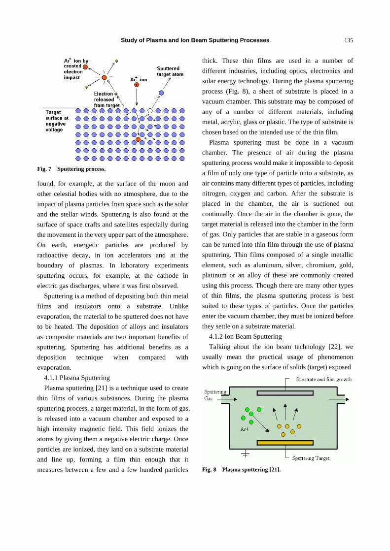
4.1.1 Plasma Sputtering Plasma sputtering [21] is a technique used to create
thin films of various substances. During the plasma sputtering process, a target material, in the form of gas, is released into a vacuum chamber and exposed to a high intensity magnetic field. This field ionizes the atoms by giving them a negative electric charge. Once particles are ionized, they land on a substrate material and line up, forming a film thin enough that it measures between a few and a few hundred particles
thick. These thin films are used in a number of different industries, including optics, electronics and solar energy technology. During the plasma sputtering process (Fig. 8), a sheet of substrate is placed in a vacuum chamber. This substrate may be composed of any of a number of different materials, including metal, acrylic, glass or plastic. The type of substrate is chosen based on the intended use of the thin film.
Plasma sputtering must be done in a vacuum chamber. The presence of air during the plasma sputtering process would make it impossible to deposit a film of only one type of particle onto a substrate, as air contains many different types of particles, including nitrogen, oxygen and carbon. After the substrate is placed in the chamber, the air is suctioned out continually. Once the air in the chamber is gone, the target material is released into the chamber in the form of gas. Only particles that are stable in a gaseous form can be turned into thin film through the use of plasma sputtering. Thin films composed of a single metallic element, such as aluminum, silver, chromium, gold, platinum or an alloy of these are commonly created using this process. Though there are many other types of thin films, the plasma sputtering process is best suited to these types of particles. Once the particles enter the vacuum chamber, they must be ionized before they settle on a substrate material.
4.1.2 Ion Beam Sputtering Talking about the ion beam technology [22], we
usually mean the practical usage of phenomenon which is going on the surface of solids (target) exposed
Fig. 8 Plasma sputtering [21].
Study of Plasma and Ion Beam Sputtering Processes
136
in vacuum under the directed flow of atomic particles - ions or neutrals. These ions are extracted from gas discharge plasma as the spatially restricted beam and accelerated by the electric field to the required energies. The discharge plasma is generated inside the special device (ion source). Ion beam sputtering utilizes an ion source to generate a relatively focused ion beam directed at the target to be sputtered. The ion source consists of a cathode and anode with a common central axis. Applying a high voltage field of 2-10 kV to the anode creates an electrostatic field inside the ion source, confining electrons around a saddle point in the center of the source. When argon gas is injected into the ion source, the high electric field causes the gas to ionize, creating plasma inside the source region. The ions are then accelerated from the anode region to the exit aperture (cathode) creating a “collimated” ion beam. The resulting ion beam impinges upon a target material and, via momentum transfer between the ion and the target, sputters this material onto the sample. Ion beam sputtered films have many advantages over other sputtering methods used in EM (electron microscopy). Since the coating material is passed into the vapor phase by a mechanical rather than a chemical or thermal process, virtually any material can be deposited on the sample. This flexibility makes ion beam sputtered films ideal for a variety of analytical techniques used in EM. Another by product of the physical sputtering process is the lack of thermal radiation presented to the sample, allowing heat sensitive samples to be processed. This is in direct contrast to magnetron methods where samples are exposed to high energy ion bombardment, electron flux, and high temperatures. Ion beam sputtering is also a highly controllable process due to the lower deposition rates when compared with magnetron methods.
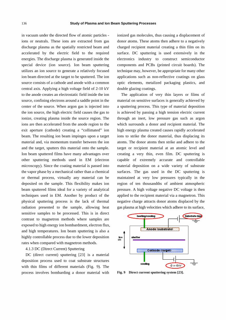
4.1.3 DC (Direct Current) Sputtering DC (direct current) sputtering [23] is a material
deposition process used to coat substrate structures with thin films of different materials (Fig. 9). The process involves bombarding a donor material with
ionized gas molecules, thus causing a displacement of donor atoms. These atoms then adhere to a negatively charged recipient material creating a thin film on its surface. DC sputtering is used extensively in the electronics industry to construct semiconductor components and PCBs (printed circuit boards). The technique may, however, be appropriate for many other applications such as non-reflective coatings on glass optic elements, metalized packaging plastics, and double glazing coatings.
The application of very thin layers or films of material on sensitive surfaces is generally achieved by a sputtering process. This type of material deposition is achieved by passing a high tension electric current through an inert, low pressure gas such as argon which surrounds a donor and recipient material. The high energy plasma created causes rapidly accelerated ions to strike the donor material, thus displacing its atoms. The donor atoms then strike and adhere to the target or recipient material at an atomic level and creating a very thin, even film. DC sputtering is capable of extremely accurate and controllable material deposition on a wide variety of substrate surfaces. The gas used in the DC sputtering is maintained at very low pressures typically in the region of ten thousandths of ambient atmospheric pressure. A high voltage negative DC voltage is then applied to the recipient material via a magnetron. This negative charge attracts donor atoms displaced by the gas plasma at high velocities which adhere to its surface,
Fig. 9 Direct current sputtering system [23].
Study of Plasma and Ion Beam Sputtering Processes
137
thus forming the film. This type of material deposition has no negative effects on the recipient or film materials and is ideal for applications in the semiconductor industry. The highly accurate thin coating made possible with DC sputtering allows for the very precise films required for PCB and component construction. The DC sputtering process is also used in the production of many other coated products. Non-reflective coatings on optics for binoculars and telescopes are applied with this technique as are those used in double glazed window panes. Plastics such as those to package chips and snacks are also coated with a metallic film using DC sputtering. Other common uses of sputtering are the hard nitride coatings on tool bits and metallic coatings on CD and DVD discs. Computer hard drives and solar cells are also coated with various metallic films using DC sputtering processes.
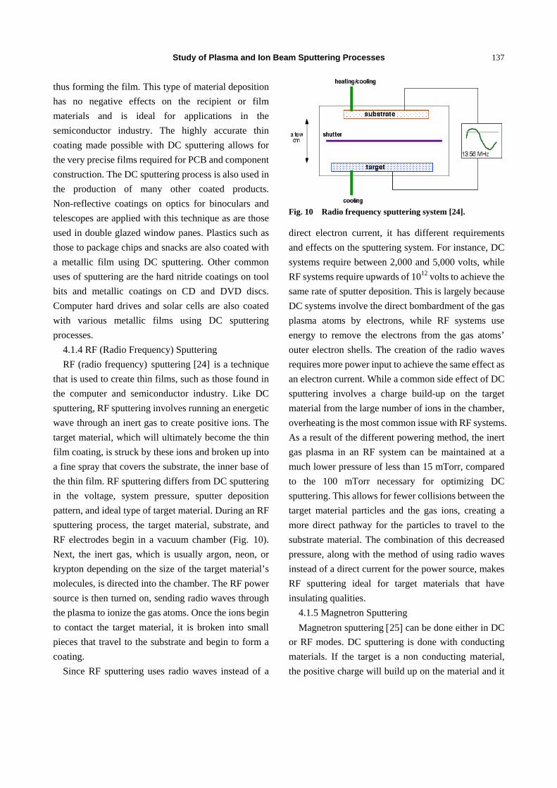
4.1.4 RF (Radio Frequency) Sputtering RF (radio frequency) sputtering [24] is a technique
that is used to create thin films, such as those found in the computer and semiconductor industry. Like DC sputtering, RF sputtering involves running an energetic wave through an inert gas to create positive ions. The target material, which will ultimately become the thin film coating, is struck by these ions and broken up into a fine spray that covers the substrate, the inner base of the thin film. RF sputtering differs from DC sputtering in the voltage, system pressure, sputter deposition pattern, and ideal type of target material. During an RF sputtering process, the target material, substrate, and RF electrodes begin in a vacuum chamber (Fig. 10). Next, the inert gas, which is usually argon, neon, or krypton depending on the size of the target material’s molecules, is directed into the chamber. The RF power source is then turned on, sending radio waves through the plasma to ionize the gas atoms. Once the ions begin to contact the target material, it is broken into small pieces that travel to the substrate and begin to form a coating.
Since RF sputtering uses radio waves instead of a
Fig. 10 Radio frequency sputtering system [24].
direct electron current, it has different requirements and effects on the sputtering system. For instance, DC systems require between 2,000 and 5,000 volts, while RF systems require upwards of 1012 volts to achieve the same rate of sputter deposition. This is largely because DC systems involve the direct bombardment of the gas plasma atoms by electrons, while RF systems use energy to remove the electrons from the gas atoms’ outer electron shells. The creation of the radio waves requires more power input to achieve the same effect as an electron current. While a common side effect of DC sputtering involves a charge build-up on the target material from the large number of ions in the chamber, overheating is the most common issue with RF systems. As a result of the different powering method, the inert gas plasma in an RF system can be maintained at a much lower pressure of less than 15 mTorr, compared to the 100 mTorr necessary for optimizing DC sputtering. This allows for fewer collisions between the target material particles and the gas ions, creating a more direct pathway for the particles to travel to the substrate material. The combination of this decreased pressure, along with the method of using radio waves instead of a direct current for the power source, makes RF sputtering ideal for target materials that have insulating qualities.
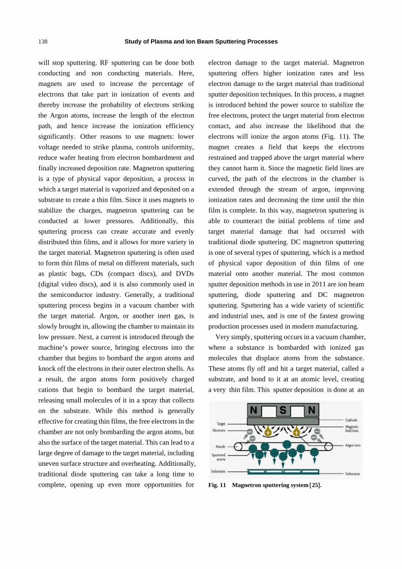
4.1.5 Magnetron Sputtering Magnetron sputtering [25] can be done either in DC
or RF modes. DC sputtering is done with conducting materials. If the target is a non conducting material, the positive charge will build up on the material and it
Study of Plasma and Ion Beam Sputtering Processes
138
will stop sputtering. RF sputtering can be done both conducting and non conducting materials. Here, magnets are used to increase the percentage of electrons that take part in ionization of events and thereby increase the probability of electrons striking the Argon atoms, increase the length of the electron path, and hence increase the ionization efficiency significantly. Other reasons to use magnets: lower voltage needed to strike plasma, controls uniformity, reduce wafer heating from electron bombardment and finally increased deposition rate. Magnetron sputtering is a type of physical vapor deposition, a process in which a target material is vaporized and deposited on a substrate to create a thin film. Since it uses magnets to stabilize the charges, magnetron sputtering can be conducted at lower pressures. Additionally, this sputtering process can create accurate and evenly distributed thin films, and it allows for more variety in the target material. Magnetron sputtering is often used to form thin films of metal on different materials, such as plastic bags, CDs (compact discs), and DVDs (digital video discs), and it is also commonly used in the semiconductor industry. Generally, a traditional sputtering process begins in a vacuum chamber with the target material. Argon, or another inert gas, is slowly brought in, allowing the chamber to maintain its low pressure. Next, a current is introduced through the machine’s power source, bringing electrons into the chamber that begins to bombard the argon atoms and knock off the electrons in their outer electron shells. As a result, the argon atoms form positively charged cations that begin to bombard the target material, releasing small molecules of it in a spray that collects on the substrate. While this method is generally effective for creating thin films, the free electrons in the chamber are not only bombarding the argon atoms, but also the surface of the target material. This can lead to a large degree of damage to the target material, including uneven surface structure and overheating. Additionally, traditional diode sputtering can take a long time to complete, opening up even more opportunities for
electron damage to the target material. Magnetron sputtering offers higher ionization rates and less electron damage to the target material than traditional sputter deposition techniques. In this process, a magnet is introduced behind the power source to stabilize the free electrons, protect the target material from electron contact, and also increase the likelihood that the electrons will ionize the argon atoms (Fig. 11). The magnet creates a field that keeps the electrons restrained and trapped above the target material where they cannot harm it. Since the magnetic field lines are curved, the path of the electrons in the chamber is extended through the stream of argon, improving ionization rates and decreasing the time until the thin film is complete. In this way, magnetron sputtering is able to counteract the initial problems of time and target material damage that had occurred with traditional diode sputtering. DC magnetron sputtering is one of several types of sputtering, which is a method of physical vapor deposition of thin films of one material onto another material. The most common sputter deposition methods in use in 2011 are ion beam sputtering, diode sputtering and DC magnetron sputtering. Sputtering has a wide variety of scientific and industrial uses, and is one of the fastest growing production processes used in modern manufacturing.
Very simply, sputtering occurs in a vacuum chamber, where a substance is bombarded with ionized gas molecules that displace atoms from the substance. These atoms fly off and hit a target material, called a substrate, and bond to it at an atomic level, creating a very thin film. This sputter deposition is done at an
Fig. 11 Magnetron sputtering system [25].
Study of Plasma and Ion Beam Sputtering Processes
139
atomic level, so the film and the substrate have a virtually unbreakable bond and the process produces a film that is uniform, extremely thin and cost effective. Magnetrons are used in the sputtering process to help control the path of the displaced atoms that fly randomly around the vacuum chamber. The chamber is filled with a low-pressure gas, frequently argon, and several high-voltage magnetron cathodes are placed behind the coating material target. High voltage flows from the magnetrons across the gas and creates high-energy plasma that strikes the coating material target. The force generated by these plasma ion strikes causes atoms to eject from the coating material and bond with the substrate. The atoms that are ejected in the sputtering process usually fly through the chamber in random patterns. Magnetrons produce high-energy magnetic fields that can be positioned and manipulated to collect and contain the generated plasma around the substrate. This forces the ejected atoms to travel predictable paths to the substrate. By controlling the path of the atoms, the film deposition rate and thickness can also be predicted and controlled. Radio frequency magnetron sputtering, also called RF magnetron sputtering is a process that is used to make thin film. This process is useful for making thin films out of materials that are non-conductive. In RF magnetron sputtering, a thin film is grown on a substrate that is placed in a vacuum chamber. Powerful magnets are used to ionize the target material and encourage it to settle on the substrate in the form of a thin film. The first step in the RF magnetron sputtering process is to place a substrate material in a vacuum chamber. Once the substrate is placed in the vacuum chamber, the air is removed and the target material, the material that will comprise the thin film, is released into the chamber in the form of a gas. Particles of the target material are ionized through the use of powerful magnets. Now in the form of plasma, the negatively charged target material lines up on the substrate to form a thin film. Thin films can range in thickness from a few to a few hundred atoms or molecules. The magnets used in the
RF magnetron sputtering process help speed up the growth of the thin film. Magnetizing atoms helps to increase the percentage of target material that becomes ionized. Ionized atoms are more likely to interact with the other particles involved in the thin film process and are, thus, more likely to settle on the substrate. Magnetizing the particles increases the efficiency of the thin film process, allowing thin films to grow more quickly and at lower pressures. The RF magnetron sputtering process is especially useful for making thin films out of materials that are non-conducting. These materials may have more difficulty forming into a thin film because they become positively charged without the use of magnetism. Atoms with a positive charge will slow down the sputtering process and can “poison” other particles of the target material, further slowing down the process.
5 Applications of Sputtering
Sputtering has long been regarded just as an undesired effect which destroys cathodes and grids in gas discharge tubes and ion sources. In high temperature plasma experiments with respect to controlled thermonuclear fusion, sputtering contributes to thinning of the vessel walls and a contamination of the hot hydrogen plasma with atoms of the vessel walls, which represents a major problem in fusion research [26]. Sputtering is one of the causes for the destruction of diaphragms and targets in accelerators and in high-voltage electron microscopes. In ion implantation, the simultaneous removal of surface atoms by sputtering limits the achievable concentration in the implantation range. However today, sputtering is used for many applications and has become an indispensable process in modern technology and physics. Both the removal of atoms from a surface and the flux of atoms leaving the surface are successfully applied. Sputtering allows a controlled removal of surface layers on a nearly atomic scale. It is applied for obtaining clean surfaces in FEM (field electron microscopy), FIM (field ion microscopy), LEED (low energy electron
Study of Plasma and Ion Beam Sputtering Processes
140
diffraction) and Auger analysis of surfaces [27]. An intense ion beam with a geometrical sharp edge is used for nearly destruction free cuts for analysis of thick films such as in ion beam slope cutting. The controlled erosion with well-focused ion beams is especially useful for optical components, lenses and even large mirrors of glasses and some insulators such as SiC [28]. The topography of the mechanically polished surface is analyzed with optical interferometry. The surface is finally machined and polished with a computer-controlled ion beam resulting in a submicron spatial resolution. With noble gas ion beams in the 100 eV range or gas clusters with noble gas atoms at energies in the 100 eV range, the surfaces are polished or nanostructured on an atomic scale. Sputtering is further applied for surface analysis and depth profiling of thin films. The ions removed by sputtering as well as the removed atoms after ionization can be analyzed in a mass spectrometer such as in SIMS or SNMS, and this gives very sensitive information about the surface concentrations, and a depth profile [29]. With mastered primary ion beams or imaging of the sputtered ions, a high spatial resolution can be achieved. If the surface is
firstly smoothed by noble gas ion sputtering and sample rotation, a very good depth resolution can be obtained. One of the largest applications of sputtering is, however, the deposition of thin films on a large variety of substrates, onto large areas of several m2 or onto extremely small areas such as in microelectronics. The composition and properties of the deposited films depend on the deposition process, such as short or long pulsed or continuous sputtering of the substrate and the residual gas pressure during deposition.
6. Theoretical Treatment for Ion Sputtering
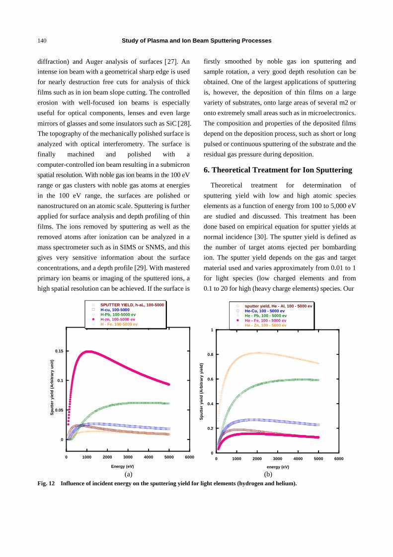
Theoretical treatment for determination of sputtering yield with low and high atomic species elements as a function of energy from 100 to 5,000 eV are studied and discussed. This treatment has been done based on empirical equation for sputter yields at normal incidence [30]. The sputter yield is defined as the number of target atoms ejected per bombarding ion. The sputter yield depends on the gas and target material used and varies approximately from 0.01 to 1 for light species (low charged elements and from 0.1 to 20 for high (heavy charge elements) species. Our
0
0.05
0.1
0.15
0 1000 2000 3000 4000 5000 6000
Data 2,hydrogen
SPUTTER YIELD, h-aL, 100-5000H-cu, 100-5000H-Pb, 100-5000 evH-zn, 100-5000 evH - Fe, 100-5000 ev
Sput
ter y
ield
(Arb
itrar
y un
it)
Energy (eV)
0
0.2
0.4
0.6
0.8
1
0 1000 2000 3000 4000 5000 6000
Data 4, Helium
sputter yield, He - Al, 100 - 5000 evHe-Cu, 100 - 5000 evHe - Pb, 100 - 5000 evHe - Fe, 100 - 5000 evHe - Zn, 100 - 5000 ev
Sput
ter y
ield
(Arb
itrar
y yi
eld)
energy (eV) (a) (b)
Fig. 12 Influence of incident energy on the sputtering yield for light elements (hydrogen and helium).
Study of Plasma and Ion Beam Sputtering Processes
141
0
2
4
6
8
10
12
0 1000 2000 3000 4000 5000 6000
Data 1, argon
sputter yield, Ar-Al, 100-5000 evAr-Cu, 100-5000Ar-Fe, 100-5000Ar-pb, 100-5000Ar-zn, 100-5000
sput
ter y
ield
(Arb
itrar
y un
it)
energy, ev
0
5
10
15
20
0 1000 2000 3000 4000 5000 6000
Kr- Fe, 100-5000 evKr -Cu, 100 - 5000 Kr - Pb, 100 - 5000 evKr - Al, 100 - 5000 evKr - Zn, 100 - 5000 ev
Sput
ter y
ield
(Arb
itrar
y un
it)
Energy (ev) (a) (b)
0
1
2
3
4
5
6
0 1000 2000 3000 4000 5000 6000
Data 4, oxygen
sputter yield, O-Zn, 100 - 5000 evO - Al, 100 - 5000 evO - Pb, 100 - 5000 evO - Cu, 100 - 5000 evO - Fe, 100 - 5000 ev
Sput
ter y
ield
(Arb
itrar
y yi
eld
)
energy (eV)
0
1
2
3
4
5
6
7
0 1000 2000 3000 4000 5000 6000
Data 5, Neon (Ne)
sputter yield, Ne - Al, 100 - 5000 evNe - Cu, 100 - 5000 evNe - Fe, 100 - 5000 evNe - Pb, 100 - 5000 evNe - Zn, 100 - 5000 ev
Sput
ter y
ield
(Arb
itrar
y un
it)
energy (eV) (c) (d)
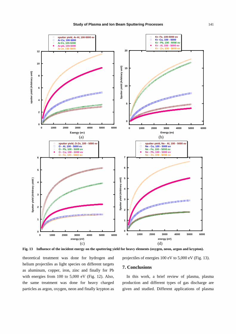
Fig. 13 Influence of the incident energy on the sputtering yield for heavy elements (oxygen, neon, argon and krypton).
theoretical treatment was done for hydrogen and helium projectiles as light species on different targets as aluminum, copper, iron, zinc and finally for Pb with energies from 100 to 5,000 eV (Fig. 12). Also, the same treatment was done for heavy charged particles as argon, oxygen, neon and finally krypton as
projectiles of energies 100 eV to 5,000 eV (Fig. 13).
7. Conclusions
In this work, a brief review of plasma, plasma production and different types of gas discharge are given and studied. Different applications of plasma
Energy (ev)

Study of Plasma and Ion Beam Sputtering Processes
142
sources are discussed and investigated. Furthermore, technique of ion beam extraction from
a plasma source for sputtering process by using a suitable electrode is carefully studied and given. In a furthermore consequence, a general review about the physics and mechanism of sputtering processes is studied. Different types of sputtering techniques are investigated and clarified.
Theoretical treatment for determination of sputtering yield for low and high atomic species elements as a function of energy from 100 to 5,000 eV are studied and discussed. It was found that for a light particle, the sputtering yield is small (0.01 to 1) while for a heavy particles is very large (0.1 to 20). Finally, various applications of plasma-and-ion beam sputtering have also been mentioned and discussed.
References
[1] Brown, I. G., ed. 2004. The Physics and Technology of Ion Sources. New York: John Wiley & Sons.
[2] Wolf, B. H. 1995. Handbook of Ion Sources. New York: CRC press.
[3] Amaldi, U. 2000. Euro physics News 31. [4] Wilson, R. G., and Brewer, G. R. 1973. Ion Beams with
Applications to Ion Implantation. New York: John Wiley. [5] Chen, F. 2003. “Evolution of RF plasma sources.” In 50th
AVS symposium. [6] Mathur, D., ed. 1991. Physics of Ion Impact Phenomena.
Berlin Heidelberg: Springer-Verlag. [7] Xie, Z., Lyneis, C. M., Lam, R. S., and Lundgren, S. A.
1991. Rev. Sci. Instrum. 62: 775. [8] Nakagawa, T., et al. 1993. Jpn. J. Appl. Phys. 32 L: 1335. [9] Biri, S., et al. 2000. Rev. Sci. Instrum. 71: 869. [10] Mironov, V., et al. 2001. Rev. Sci. Instrum. 72: 3826.
[11] Nakagawa, T., et al. 1998. Jpn. J. Appl. Phys. 37: 2699. [12] Gammino, S., Sijbring, J., and Drentje, A. G. 1992. Rev.
Sci. Instrum. 63: 2872. [13] Leitner, M., Wutte, D., Brandstötter, J., Aumayr, F., and
Winter, HP. 1994. Rev. Sci. Instrum. 65: 1091. [14] Drentje, A. G., et al. 2004. Rev. Sci. Instrum. 75: 1399. [15] Hassan, A., et al. 2007. Rev. Sci. Instrum. 78: 123301. [16] Winter, HP. 1978. “Production of Multiply Charged
Heavy Ions.” In Lecture notes in Physics, edited by Bethge, K. Berlin: Springer, 83: 2-80.
[17] Duchemin, O. B. 2001. PhD. Thesis, California Institute of Technology, Pasadena, California, USA.
[18] Behrisch, R., Eckstein, W. (Eds.). 2007. “Sputtering by Particle Bombardment.” Topics Appl. Physics 110: 1-20.
[19] Septier, A. 1967. Focusing of Charged Particles, Vol. II. New York: Academic press.
[20] Loeb, H. W. 2005. Plasma Phys. Control. Fusion 47: B565-B576.
[21] Aumayr, F., and Winter, HP. 2004. “Potential Sputtering.” Philosophical Transactions of the Royal Society London A 362: 77-102.
[22] Valyi, L. 1977. Atom and Ion Sources. New York: John Wiley & Sons.
[23] Li, G. Q., et al. 2005. Surface & Coatings Technology 193: 112-6.
[24] Derwen Lee, E. 2009. MSc Thesis, University of Illinois at Urbana-Champaign, Urbana, Illinois.
[25] Anders, A. 2005. Surface & Coatings Technology 200: 1893-1906.
[26] Baragiola, R. A. 2004. Phil. Trans. R. Soc. Lond. A 362: 29-53.
[27] Abdelrahman, M. M. 2010. Brazilian Journal of Physics 40: 1.
[28] Chu, P. K., et al. 2002. Materials Science and Engineering R 36: 143-206.
[29] Michael, J. G. 2004. PhD. Thesis, California Institute of Technology, Pasadena, California, USA.
[30] Matsunami, N., et al. 1984. Atomic Data and Nuclear Data Tables 31: 1-80.