Embed Size (px)
Citation preview

1
STUDY OF ORGANIC MATERIALS AND PLASMA
PROCESSING FOR NUCLEAR RADIATION
DETECTORS
By
ARINDAM RAY
(Enrolment No: PHYS01201304019)
Bhabha Atomic Research Centre, Mumbai
A thesis submitted to the
Board of Studies in Physical Sciences
In partial fulfillment of requirements
for the Degree of
DOCTOR OF PHILOSOPHY
of
HOMI BHABHA NATIONAL INSTITUTE
November, 2018

2

3

4
5
List of Publications arising from the thesis
Journal
1. “Development of stable nuclear radiation detectors based on n-silicon/cobalt-phthalocyanine heterojunctions”, A.Ray, R.Prasad, C.A.Betty, T.V.Chandrasekhar Rao, Radiation Physics and Chemistry, 2016, 120, 12-16. 2. “Development of surface barrier detectors of low leakage current employing argon cold plasma assisted silicon surface cleaning prior to detector fabrication”, A.Ray, Tomi Nath Das, C.A.Betty and T.V.Chandrasekhar Rao, Journal of
Instrumentation (JINST), 2018, 13 P09019. 3. “Junction edge passivation study of silicon surface barrier detectors using organic films deposited by L-B technique”, A.Ray, Sipra Choudhury, Vishal Singh, C.A.Betty and T.V.Chandrasekhar Rao, Bulletin of Material Science (accepted).
Not included in the thesis but very much referred 4. “Nuclear detectors based on n-silicon/copper-phthalocyanine heterojunctions”, A.Ray, S.K.Gupta, J.V.Yakhmi, Radiation Measurements, 2009, 44, 47-49.
Conferences
1. “Junction edge passivation study of silicon surface barrier detectors using organic films deposited by L-B technique”, A.Ray, Sipra Choudhury, C.A.Betty and T.V.Chandrasekhar Rao [Presented the paper in M-TECS 2018
conference, September26-29, 2018, Organised by MRSI, Mumbai Chapter and Sponsored by Board of Research in Nuclear Science, DAE].
2. “Polymer based detectors: A preliminary study”, A.Ray, Proc. of the DAE-
BRNS Symposium on Nucl. Phys., 2015, 60, 956-957. [Available online at www.sympnp.org/proceedings].
3. “Development of Rugged Silicon Surface Barrier Detector”, A.Ray, Shovit Bhattacharya, Ranu Bhatt, D.K.Aswal, S.K.Gupta, 31
st IARP National
Conference on Advances in Radiation Measurement Systems and Techniques
(IARPNC-2014), 2014, p.-269. 4. “Fabrication of Ultra-thin Oxide-passivated Silicon Surface Barrier Detectors”,
A.Ray, D.K.Aswal, R.Prasad, S.K.Gupta, Proc. of the DAE Symp. on Nucl.
Phys., 2013, 58, 848-849. [Available online at www.sympnp.org/proceedings]. 5. “Study of Aging of Nuclear Detector Based on n-Slicon/Copper-
Phthalocyanine Heterojunction”, A.Ray, S.K.Gupta, AIP Conference Proc.
(DAE SSPS-2012), 2013, 1512, 458-459.
Arindam Ray

6
Dedicated to my parents, wife and children

7
ACKNOWLEDGEMENTS
To begin with, from the bottom of my heart, I am expressing my sincere gratitude to
my research guide Dr. (Smt.) C.A.Betty, Scientific Officer (G), Chemistry Division,
Bhabha Atomic Research Centre (BARC), Mumbai, who despite her preoccupations
was kind enough to accommodate me as her research student and was always willing
to make herself available for my thesis work. It is her immense support which has
actually made it possible for me to complete this thesis.
It is my pleasure to express my grateful thanks to Dr.A.K.Mohanty, Director-
Physics Group, BARC for his continuous encouragement and support.
I must offer my gratitude and respect to my present Section Head, Dr.
T.V.Chandrasekhar Rao for his continuous support, guidance and encouragement in
carrying out this work.
I’m very much indebted to Dr.S.K.Gupta, DAE – Raja Ramanna Fellow (Ex-
Head, Technical Physics Division and Ex-Associate Director, Physics Group, BARC)
for not only giving support but also for his constant encouragement and valuable
guidance. He is also Chairman of my doctoral committee.
I’m greatly indebted to Dr.B.K.Nayak, Nuclear Physics Division and also Dean-
Academic, Physical Science, HBNI, who despite his preoccupations was kind enough
and attended all my presentations before my doctoral committee as an Honourable
invitee. He is a constant source of encouragement to me.
I’m also very much grateful to all other doctoral committee members and invitees
viz. Prof. Senthil Kumar, IIT-Bombay, Dr. D.C.Biswas, Dr. Bency V.John and
Dr.(Smt.) Anita Topkar. At this juncture I must name two more personalities who
8
actually created my interest in the field of Nuclear Radiation Detectors and they are
my Ex-Section Heads Dr.R.V.Srikantiah and Dr.D.Sahoo.
I’m highly grateful to Dr.D.K.Aswal, Director-NPL, CSIR, New Delhi for his
tremendous help and support.
I’m highly thankful to my very good friends and well-wishers Dr. A.K.Chauhan,
and Dr. A.K.Debnath from Technical Physics Division, BARC for motivating me all
the time as well as giving their best support and valuable suggestions.
I’m very much thankful to Dr. Swapan Das, Nuclear Physics Division, for
offering many valuable suggestions that has greatly helped me to complete this work.
I must express my sincere thanks to Dr. S.C.Gadkari, Dr. R.Tewari, Shri
M.Gopalkrishna, Shri T.K.Saha, Dr. K.P.Muthe, Shri R.Prasad, Dr. R. Ganguly,
Dr. T.N.Das, Dr. Sipra Choudhury, Shri P.G.Abichandani, Shri V.Nataraju, Shri
E.Ravishankar, Dr. K.G.Bhushan, Dr. Jagannath, Shri Manish Kumar, Shri V.Parayya,
Shri A.Kasbekar, Shri Sunil Sahu, Smt. Nivedita Ved, Shri Sandip Chowdhury, Smt.
Deepa Bhambure, Smt. Alka Satam, Shri B.A.Narayanan and Smt. Pushpa Panchal for
extending support and help at various stages of the thesis work.
I take this opportunity to record my sincere gratitude to all my teachers. Also, it
gives me great pleasure to acknowledge all my friends for their invaluable support all
along.
Last but not the least, I would like to acknowledge my whole-hearted
indebtedness to my parents, and to my wife Suparna who have always cheered and
supported me when things seemed to become burdensome. Their love has provided
me energy to move forward.
Arindam Ray

9
To My Guide

10
CONTENTS
Page No.
SYNOPSIS 11-18
CHAPTER 1 Introduction
19-45
CHAPTER 2
CHAPTER 3
CHAPTER 4
CHAPTER 5
Development of stable nuclear detectors based on
Au/Organic thin film/n-Si structures
Si-surface barrier detectors using
Organic/Inorganic thin films as passivation layer
Development of improved surface barrier
detectors by employing argon cold plasma
assisted Silicon surface cleaning
Purely organic radiation sensors
46-60
61-82
83-97
98-107
CHAPTER 6 Conclusion and future scope 108-111
REFERENCES
112-117
11
SYNOPSIS
Detection, identification and measurement of energy of ionizing radiations are
very important in the research on nuclear science and technology. It also plays an
important role in the development of medical diagnostics and in the study of cosmic
ray effects etc. A variety of nuclear detectors have been developed over the years to
fulfill this task. The charged particle detectors (e.g. Silicon Surface Barrier Detectors)
find wide spread use among these applications. This very fact necessitates
development of high quality (viz. low leakage current, high resolution, highly reliable
in terms of their long term stability etc.) detectors and this activity has been an active
as well as an important field for scientific investigations. Fabrication of high quality
detectors demands stringent selection of detection material. To be very specific, the
material should be of high resistivity (for larger depletion depth), small band gap (for
good energy resolution), indirect band gap (high life time of carriers), high charge
carrier mobility and life time (for good charge collection), availability of single
crystals in large sizes (for good efficiency), should be easy to make stable electrical
contact and lastly the material should have minimum trapping centers (for good
charge collection). Silicon fulfills all the above requirements and is considered as one
of the key detection materials.
In recent years, demand for high quality silicon detectors has greatly enhanced
worldwide, especially for high-energy physics experiments (e.g. CMS experiment at
CERN etc.). But the common problem always arises is that the fabricated silicon
detectors breaks down at much lower reverse voltage as compared to its bulk
breakdown voltage, though one chooses a very high resistivity silicon. The reason
attributed to this is none other than highly active nature of silicon surface (as the

12
number of surface states in silicon is 2 – 4 × 10¹⁵/cm2) and the breakdown of silicon
detectors at much lower voltage than bulk breakdown is due to surface breakdown
which results in very high reverse leakage current. To prevent this surface breakdown,
silicon surface needs to be passivated. Currently the leakage currents are reduced by
passivating the edges either by epoxy or by silicon dioxide. Apart from these two, new
passivating materials also are being explored to fabricate detectors with improved
properties. Another important parameter for the good performance of the detectors is
energy resolution. There are a number of factors which can affect the energy
resolution of silicon based nuclear detectors viz. spectral broadening due to: (i)
statistical fluctuation in number of ion pairs produced, (ii) nuclear collision, (iii)
detector and amplifier noise, (iv) specifications of the radiation source and (v)
detector dead layer. As a detector developer, one can improve energy resolution (a) by
reducing detector capacitance (i.e. by fabricating a detector of smaller active area)
which will bring down detector noise and/or (b) by reducing leakage current and/or (c)
by minimizing dead layer. Bringing down the leakage current and to get longevity for
good performance of fabricated detectors is a challenging task for a detector
developer. This prompted the author to take up the theme of the present thesis
which is mainly aimed to explore alternate organic materials and processes to
reduce leakage, since higher leakage current in silicon radiation detectors limits
the detector performance as well as longevity.
Silicon based α particle and heavy ion detectors, especially surface barrier
detectors – both partially depleted as well as thin and fully depleted – play an
important role in low to moderate energy physics experiments in accelerators. These
detectors are having numerous advantages namely, excellent energy resolution,

13
particle identification, linear energy response, variety of configuration, compact and
small power requirements. These detectors work on the principle of ionization in solid
medium by the incident radiation which is followed by collection of electron-hole
pairs (EHP). One of the major issues in many silicon detectors is the high leakage
current through edges of Si/metal junction. So far the leakage currents were reduced
by passivating the edges either by epoxy or by silicon dioxide. Silicon dioxide
passivated Silicon detectors are known for their long term stability. However,
oxidizing Silicon with an aim to get good quality thin SiO2 layer (breakdown voltage:
7 Mega Volt/cm) requires high temperature (1000-1200ºC) oxidation furnace, high
quality oxygen etc. Though organic epoxy passivated detectors are very much present
in the market, epoxy has a disadvantage as it is hydrophilic in nature and reacts with
moisture over a period of time to give rise to more leakage current and therefore
affects long term stability. We have already developed a number of organic and oxide
passivated silicon E and delta E detectors. Few rugged silicon surface barrier detectors
with organic epoxy passivation were also developed. In order to have a simpler
fabrication procedure for the detectors, it is essential to look for new passivating
materials, which can be deposited at the edges of silicon wafer at a relatively lower
temperature and slow/negligible degradation with atmospheric exposure. Growing
SnO2 film on a Silicon wafer by initially depositing Octa Decyl Amine-Stannate
Complex (ODA-Stannate complex) with the help of Langmuir-Blodgett (LB)
deposition technique followed by heating the sample in a furnace at a relatively low
temperature (600ºC) to decompose the LB layer to form SnO2 film on Silicon is a new
as well as simpler technique which has been explored to study passivation of Silicon
detectors. As tin oxide layer grown by this method consist of SnO2 nano particles

14
which are not affected by humidity, the layer behaves like a depletion layer and offers
very high resistance. Further, in few silicon samples hydrogenated amorphous silicon
as a passivating layer has also been studied. In addition, possibilities of using organic
semiconductors (CuPc, CoPc) and silicon heterojunction structures for α-detectors
have been thoroughly investigated.
Semiconducting organic material can be subdivided into three categories,
namely, polymers, oligomers and small molecules depending on the length of the
molecular structure. This very molecular structure actually establishes the mechanical,
chemical and electronic properties of the organic materials. Since, the radiation
creates charge carrier inside polymer matrix by ionizing the medium, these charge
carriers can be utilized for the detection of radiation. The motive behind these studies
is to tap the advantages of organic based devices (the ease of fabrication, improved
performance in terms of low leakage and long term stability etc.) for α detectors.
Some preliminary studies were also carried out to explore new polymer
viz. Bi-axially oriented Poly Ethylene Terephthalate (BoPET) based α-sensor which
will help to design new polymer based flexible and easily portable α detector at low
cost. Additionally, surface barrier detectors of reasonably good performance were
fabricated and exhaustively studied by incorporating cold plasma assisted silicon
surface cleaning (keeping aside the existing cleaning methods, e.g. cleaning of silicon
surface by organic solvents and RCA cleaning of silicon surface etc. which are
exhaustive and time consuming) prior to edge protection using organic epoxy
followed by metallization.
The thesis has been organized into six chapters as summarized below:

15
Chapter 1, Introduction: This chapter includes an introductory discussion on
various types of radiation, interaction of radiation with matter, radiation detection
mechanism, a comprehensive literature survey on different types of radiation detectors
with their associated problems and specifications. The thesis work mainly deals with
role of organic materials for nuclear detectors. In nuclear detectors, organic materials
can find different roles such as, (1) passivation layer in Si based alpha detectors; (2) as
an active layer in organic/Si hybrid structures and (3) pure organic material as an
active layer. Presence of organic impurities on Si, while fabricating Si surface barrier
detectors is unwanted. Therefore the removal of organic contaminants and other
impurities, by cold plasma prior to detector fabrication has also been explored. In this
thesis, extensive study has been done on all these issues.
Chapter 2, Development of stable nuclear detectors based on Au/Organic thin
film/n-Si structures: In earlier studies [A.Ray et al., Radiation Measurements, 44
(2009) 47-49], Copper phthalocyanine (CuPc) has been utilized by the author for
fabrication of nuclear detectors based on n-silicon/copper phthalocyanine
heterojunctions. Of late it has been reported that MnPc, FePc and CoPc have a
stronger binding with gold than that of NiPc, CuPc and ZnPc. So in the present study
CoPc has been used in lieu of CuPc. n-type silicon/cobalt-phthalocyanine (CoPc)
heterojunction based nuclear detectors have been fabricated using thermally
evaporated CoPc films. The detectors were characterized by measuring their current–
voltage (I–V) and leakage current–time (I–t) characteristics, followed by alpha energy
spectra obtained on exposure to α-particles. Variation of alpha energy resolution with
applied reverse bias voltage for each of the detectors was also studied. The detectors
showed very low leakage current and high breakdown voltage as compared to
16
conventional Au/n-Si surface barrier detectors. Lastly, the durability of the detectors
was established by measuring their I–V characteristics and energy resolution for
nearly 15 months
Chapter 3, Si-surface barrier detectors using Organic/Inorganic thin films as
passivation layer: In conventional Silicon Surface Barrier detectors, passivation of
surface is carried out at room temperature by using two-component epoxy. Right
quantity of Amine-based hardener is used to properly cure epoxy resin which in turn
results in very low leakage current and stable detector performance. This prompted the
author to study the use of Amine-based organic thin films as well to passivate Si
surface. It was carried out by depositing Octa Decyl Amine-Stannate Complex on the
peripheral annular region of silicon wafer at first with the help of Langmuir-Blodgett
(LB) deposition technique, followed by heating the sample in a furnace at a
temperature of 600ºC to decompose the LB layer to form SnO2 film on Silicon. Tin
oxide layer so grown consists of SnO2 nano-particles. The space charge layer between
the nano-particles forms the charge carrier depletion layer and offers very high
resistance, dielectric constant and breakdown strength. Growing SnO2 film on a
Silicon wafer is a new as well as simpler technique which has been explored to study
passivation of Silicon detectors.
This chapter also explains the work carried out by the author towards (1)
development of oxide passivated silicon delta E detectors and (2) development of
organic epoxy passivated rugged silicon surface barrier detectors using DC sputtering
to deposit gold film on n-silicon.
Chapter 4, Development of improved surface barrier detectors by employing
argon cold plasma assisted Silicon surface cleaning: Any gas with a presence of

17
ions and chemically reactive species around 1% is known as cold plasma. In cold
plasma electron temperature is much higher than neutral and cation (i.e. other species)
temperature. That is why it is also known as non-thermal and non-equilibrium plasma.
In cold plasma, moisture is also present in small quantity. This moisture, as a result of
its interaction with high energy electron, produces [H2O]- ions which decomposes
afterwards into H+ and OH- ions. This OH- ion is highly reactive and destroys all types
of organic contaminants. This novel aspect of cold plasma has been utilized to clean
silicon surface before fabricating any device. This can be a cost effective and viable
replacement of the cleaning processes adopted by current industries for silicon surface
cleaning as cleaning using acids (piranha solution) and organic solvents are time
consuming and also may add to local environmental pollution. Surface barrier
detectors of improved performance were fabricated by incorporating the cold plasma
assisted silicon surface cleaning. It was a detector fabrication process step prior to
edge protection using epoxy and was subsequently followed by metallization. The
detectors fabricated using this new technique yielded better result compared to
detectors of same active area and processed using conventional technique. The
fabricated detectors were characterized by measuring their Current-voltage (I – V)
characteristics (both forward and reverse) and alpha energy spectra obtained on
exposure to α-particles. Variation of alpha energy resolution with applied reverse bias
voltage for each detector was also studied. The results show that the leakage current of
the new detectors treated with cold plasma formed by a mixture of Argon and Air
(90% Argon and 10% Air) was substantially lower than that of surface barrier
detectors fabricated by conventional methods.

18
Chapter 5, Purely organic radiation sensors: Two major sources of alpha
emitters, because of which environment in general and mankind in particular get
exposed are (1) uranium mining waste, and (2) concentrated natural radium which is
generated during processing phosphate ore for fertilizer. So it is essential to detect the
alpha particles in and around of such industries to prevent the environment from
getting contaminated. In the present scenario, the importance of alpha detector is not
only limited to environmental monitoring or carrying out some nuclear experiments
but also extended to prevent nuclear proliferation. For example, plutonium, an alpha
emitter, which is a classified material, can be detected by alpha detectors. For many
of these applications, it will be preferable that the radiation detectors need to be
inexpensive and flexible. Therefore it is expected that organic material based detectors,
perhaps would be best suited, for its capability to be flexible, large scale production
and that too at low cost. The working principle of organic detectors lies with the basic
fact that irradiating with ionizing radiations, conductivities in polymer materials (e.g.
BoPET etc.) can be changed. In present study, the changes in conductivities were
investigated for α-radiation detection.
Chapter 6, Conclusion and future scope: In this chapter, a summary of all the
work done is presented highlighting the main findings of this thesis. The chapter ends
by indicating some future directions that have emerged from this work.

19
________________________________________________________
Chapter 1
INTRODUCTION 1.1 Introduction
1.2 Nuclear radiation detectors
1.2.1 Nuclear radiations and radioactivity
1.2.2 A glimpse of various types of radiation detectors
1.2.3 Radiation sources
1.2.4 Interaction of nuclear radiations with matter
1.3 Semiconductor detectors
1.3.1 Successful working of a semiconductor detector needs a junction
1.3.2 Types of semiconductor junctions based on fabrication methods
1.3.3 Important development of semiconductor detectors (Chronological order)
1.3.4 Material requirement to fabricate good detector
1.3.5 Energy resolution of radiation detector
1.3.6 Factors affecting energy resolution
1.3.7 Various components of reverse leakage current
1.4 Nuclear electronics to process signals from detectors
1.4.1 Alpha spectrometer
1.4.2 Preamplifier
1.4.3 Main amplifier
1.4.4 Multi-Channel Analyzer
1.5 Scope of the thesis work

20
1.1 INTRODUCTION
Detection and energy measurement of radiation is very much important in nuclear
science and technology, medical physics and study of cosmic rays. A variety of
nuclear detectors have been developed over the years because high energy radiations
cannot be measured directly [1]. Development of nuclear radiation detectors with
improved features has opened the path for many important discoveries in nuclear
science. For example, scientists working with data from experiments at the Large
Hadron Collider (LHC), CERN (European Organization for Nuclear Research)
announced the discovery of a new particle "consistent with" the Higgs boson. It is a
subatomic particle also colloquially referred to as the "God particle." The CMS
(Compact Muon Solinoid) is a general-purpose detector which forms a part of the
LHC, is capable of studying many aspects of proton collisions at 14 trillion
electronvolts (eV). Therefore, development of better nuclear radiation detectors
continues to remain as an area of interest to many researchers. There are various kinds
of gas detectors, scintillators and semiconductor detectors [1]. These detectors are
very much useful in their respective areas of applications. Three of the oldest but at
the same time very much useful detectors are the ionization chambers, the
proportional counters and the Geiger-Muller (G – M) tube [2]. All these three are
falling in the category of Gas Detectors. Another category of detectors, also known as
scintillators, are certain materials whose atoms get ionized and/or move to excited
states when ionizing particle passes through them and during their return to the normal
states (de excitation) produce light emission, or scintillation. By employing

21
semiconductors as the basic detection medium, semiconductor radiation detectors
were developed and put to use way back in 1951[3]. Both these scintillation (mainly
inorganic scintillators e.g. NaI, CsI, BaF2) as well as semiconductor detectors are
falling in the category of solid state detectors and their dimensions can be kept smaller
(i.e. compact size) as solid densities are ~ 1000 times larger than gas [1].
Semiconductor detectors are superior to scintillators as they offer much better energy
resolution. This is achieved by reducing the statistical limit on energy resolution as a
result of generation of more number of information carrier (electron-hole pair in case
of semiconductors) per impinging charged particle/photon of the radiation.
Semiconductor detectors are used to extract the exact information about energy,
position [4] and type [5] of a nuclear radiation. Several types of semiconductor
detectors have been developed to suit different experimental requirements. The
various materials that can be utilized to fabricate nuclear radiation detectors in general
[6] and the materials pertaining to semiconductor based radiation detectors in
particular, is indeed a vast topic and will continue to remain under active
consideration to a detector developer. Over 60 years ago, in terms of radiation
detection, compound semiconductors were among the first direct detection media to
be investigated. However, material problems caused by impurities, stoichiometric
imbalances and high defect densities limited their usefulness. It is only the recent
development that substantial improvement has occurred in their material growth and
also in detector fabrication. Accordingly, compound semiconductor radiation detectors
have become serious competitors to other established radiation detectors [7]. Among
the available semiconductor materials, silicon predominates in the category of diode
detectors which are mainly used for charged particle spectroscopy. Germanium also

22
can be used for charged particle spectroscopy but Germanium detectors need to be
cooled to maintain the leakage current minimal. But for gamma ray spectroscopy, as a
semiconductor material, Germanium is more advantageous because of its higher
atomic number. Though silicon detectors can be operated at room temperature, the
common problem always arises is that the fabricated silicon detectors breaks down at
much lower reverse voltage as compared to its bulk breakdown voltage, though one
chooses a very high resistivity silicon. The reason attributed to this is none other than
highly active nature of silicon surface that leads to the breakdown of silicon detectors
at much lower voltage than bulk breakdown. This breakdown is called surface
breakdown which results in very high reverse leakage current. This leakage can be
lowered by passivating silicon surface. Currently the reduction of leakage current is
facilitated by employing edge passivation using either epoxy or silicon dioxide. Epoxy
passivation, though very simple, won’t last long as epoxy get affected by the moisture
present in air. On the other hand, oxidation of silicon to prepare SiO2 (a passivating
material more stable than epoxy) is a high temperature process and also requires
elaborate laboratory arrangement. So lots of new passivating materials/methods are
also being explored to fabricate detectors with improved properties. Other than
leakage current, another important as well as measurable parameter, what can be
considered to certify the quality of a detector is energy resolution. Moreover the
stability of the performance of the fabricated detectors is very much necessary.
Bringing down the leakage current and to get longevity for good performance of
fabricated detectors is a challenging task for a detector developer. This prompted the
author to take up the theme of the present thesis which is mainly aimed to

23
explore alternate organic materials and processes to reduce leakage and also
achieve better stability of the fabricated detectors.
In section 1.2, we discuss about nuclear radiation and radioactivity, various types
of nuclear radiation detectors, various radiation sources and interaction of nuclear
radiations with matter. In section 1.3, we describe more specifically about
semiconductor detectors along with a brief definition of energy resolution and its
dependence on various factors. In section 1.4, we present in a nutshell, the requisite
nuclear electronics which is essential for evaluation as well as functioning of the
fabricated detectors. The scope of this thesis, which mainly deals with the various
fabrication methods which resulted in reduced leakage current of developed detectors,
is presented in section 1.5.
1.2 NUCLEAR RADIATION DETECTORS
1.2.1. Radioactivity and Nuclear Radiations:
Radioactivity is a nuclear phenomenon and it is connected with the instability of the
nucleus. Since most of the elements are not radioactive, the ratio of neutron to proton
of the unstable, radioactive nucleus is the factor responsible for radioactivity.
Scientists have studied this problem exhaustively and arrived at the conclusion that the
stability or instability of a nucleus is related with the pairing of nuclear spins. It is
available in literature that electrons spin around their own axis and electron-spin
pairing leads to stable chemical bonds. Likewise inside a nucleus, protons and
neutrons too spin around their own axes and pairing of spins of protons among protons
as well as pairing of spins of neutrons among neutrons leads to nuclear stability. For
all non – radioactive i.e. stable isotopes, it is found that nuclei with even number of
protons and with even number neutrons are most abundant. The even numbers result

24
in spin pairing and odd numbers result in unpaired spins. So nuclei having either of
the proton number or the neutron number odd are slightly less stable than the even
numbered ones. The nuclei which have odd numbers of protons and odd numbers of
neutrons are the least stable ones.
In addition to the odd or even number of protons and neutrons, the nuclear stability
is also very much influenced by the neutron/proton ratio (n/p). As the number of
protons increases inside a nucleus, more and more neutrons are required to minimize
the proton-proton repulsion and eventually add to nuclear stability. As a matter of fact,
neutrons are serving as binding material inside the nucleus.
The activity of a radio isotope source is defined as its rate of decay and as per the
fundamental law of radioactive decay
( dN/dt)decay = - λN
where N is the number of radioactive nuclei and λ is called radioactive decay constant.
One of the units of activity is Curie (Ci) which is actually the activity of one gram of
pure Radium (226
Ra) and its value is 3.7 × 10¹⁰
disintegrations per second. The SI unit
of activity is Becquerel (Bq) and is defined as one disintegration per second.
1.2.2. A Glimpse of Various Types of Radiation Detectors:
There are different kinds of detectors; one can come across in literature. A majority of
them are listed below:
• Fluorescent Screen (Roentgen – discovery of X-ray)
• Photographic film and emulsion
• Cloud and bubble chamber

25
• Gas detector
• Scintillation detector
• Cerenkov detector
• Semiconductor detector
• Crystal spectrometer
• Thermoluminescence dosimeter
• Self powered neutron detector
• Solid state nuclear track detector
• Multi wire proportional counter
• Electron multipliers
• Photodiodes
• Scintillating fibres
• Microstrip detectors
• Drift detectors
• Charge Coupled Devices
• Calorimeters etc.
1.2.3 Radiation Sources:
The radiations of our concern get generated in nuclear and atomic processes. In a
broader perspective, radiations are of three kinds:
i) Charged particles (e.g. fast electrons, alpha particles and fission
fragments etc.)
ii) Uncharged particles (e.g. neutrons)
& iii) Photons (e.g. gamma and X-rays)
26
Radiation sources are also broadly considered to be of two kinds:
i) Natural (i.e. radioactive substance)
& ii) Artificial (i.e. produced due to operation of reactor and accelerator)
A. Fast electron sources
There are three different types of fast electron sources:
i) Negatively charged electrons are arising out of beta-minus decay and the process is
written schematically as:
AXz → AYZ+1 + β- + ν
where X and Y are called the parent and daughter nuclei, and ν is antineutrino. The
recoil nucleus Y comes out with a negligibly small recoil energy (< ionization
threshold). So the beta decay energy is essentially shared by neutrino/anti-neutrino
and beta particle. Beta minus emission occurs for nuclei with too many neutrons.
ii) Positively charged electrons (also known as positrons) are arising out of beta-plus
decay and the process can be written schematically as:
AXz →
AYZ-1 + β+
+ ν
where X and Y are called the parent and daughter nuclei, and ν is neutrino. Beta plus
emission occurs for nuclei with too many protons. Any beta source (i.e. β+ or β-
)
produces a continuum of energy.
Example: 22
Na (β+) and
36Cl (β-
)
iii) The nuclear process of internal conversion is the source of conversion electrons
and in certain cases they are mono-energetic. Sometimes beta decay leaves the

27
daughter nucleus in excited state and the excited nucleus cannot de-excite through
emission of γ-ray. In such cases, the nuclear excitation energy is transferred to one of
the orbital electrons and the electron comes out.
Example: 113In, 207Bi etc.
iv) Auger electrons are somewhat analogous to internal conversion electrons and
produce a discrete energy spectrum. The process of electron capture leaves an atom
with a vacancy in a normally complete electron shell. This vacancy needs to be filled
by electrons from outer shell along with emission of an X-ray. But many a times, the
excitation energy of the atom is transferred to one of the orbital electrons. As a result
of which, the electron comes out. This ejected electron is known as Auger electron.
B. Heavy charged particle sources
i) Alpha decay:
Alpha decay is schematically written as
AXZ → A-4YZ-2 + 4He2
Some heavy nuclei are spontaneous emitter of alpha particles as they are energetically
unstable against the spontaneous emission of alpha. The phenomenon called barrier
penetration mechanism is governing the probability of alpha decay. The energy of the
emitted alpha particles lies in the range between 4 – 6 MeV. It is also observed that
the alpha particle emitters emitting alpha particles of energy beyond 6 MeV are
having very short half life and those emitting alphas with energy lower than 4 MeV
are having exceedingly long half life.

28
Example: 239Pu, 241Am etc.
ii) Spontaneous fission:
All heavy nuclei are, in principle, having a tendency to undergo spontaneous fission
into two lighter fragments. But for that they need to overcome a large potential barrier.
For this reason, the spontaneous fission process is limited to few extremely heavy
nuclei.
Example: 252Cf .
C. Electromagnetic radiations
i) Gamma rays following beta decay:
Apart from emission of beta particles, beta decay ends up with an excited nucleus
which subsequently de-excites (either partly or completely) by emitting gamma rays.
But the emitted gamma rays are limited to energies below about 2.8 MeV.
Example: 22Na (1.274 MeV γ), 60Co (1.173 MeV & 1.332 MeV γ) and
137Cs (0.662 MeV γ) etc.
ii) Gamma rays following nuclear reactions:
For gamma rays of higher energies, one has to get it from nuclear reactions:
4He2 + 9Be4 → 12C6* + 1n0
4.4 MeV γ 4He2 + 13C6 → 16O8
* + 1n0 6.13 MeV γ

29
iii) Bremsstrahlung:
When fast electrons interact with matter, part of their energy comes out as
electromagnetic radiation in the form of bremsstrahlung. The part of electron energy
converted into bremsstrahlung is more for higher electron energy and for absorbing
material of high atomic number, this energy conversion becomes highest.
iv) Annihilation radiation:
The positrons coming out of β+ decay, initially looses energy in an absorbing medium.
Near the end of their range, when their energy becomes very low, they combine with
normal negative electrons in the absorber and disappear. Followed by this two
oppositely directed γ-rays of energy 0.511 MeV comes out and this process of joining
of one positron with an electron is known as annihilation.
v) Characteristics X-ray:
When the orbital electrons of an atom get disrupted from their normal configuration
due to some excitation process, it causes the atom to move to an excited state for a
short period of time. This is followed by a rearrangement of electrons amongst
themselves which in turn bring back the atom to its ground state. All these things
happen within a small time which is characteristically a nanosecond or even less for
solid material. The liberated energy in the transition from the excited state to the
ground state gets converted into a characteristics X-ray photon.
D. Neutron sources i) Spontaneous fission: In each fission of a transuranic isotope there will be emission
of few neutrons.
Example: 252Cf

30
ii) Radioisotopes: By mixing an alpha emitting isotope with an appropriate target
material a self-contained (α,n) source can be made.
Example: 4He2 +
9Be4 →
12C6 +
1n0 + 5.71 MeV
iii) Photoneutron sources: It is based on providing requisite excitation energy to the
target nucleus by way of absorption of a gamma ray photon
which results in emission of a free neutron.
Example: 9Be4 + hν → 8Be4 + 1n0 − 1.666 MeV
2H1 + hν →
1H1 +
1n0 − 2.226 MeV
iv) Reaction from accelerated charged particles:
Example: (1) Deuteron – Deuteron Reaction
2H1 + 2H1 → 3He2 + 1n0 + 3.26 MeV
(2) Deuteron – Tritium Reaction
2H1 + 3H1 → 4He2 +1n0 + 17.6 MeV
1.2.4. Interaction of Nuclear Radiation with Matter
A. Interaction of heavy charged particle
Heavy charged particles (e.g. alpha particles, fission fragments etc.) interact with
matter by exerting coulomb force on orbital electrons and nuclei of the absorber atoms.
In this process they lose energy while moving in the absorber medium. The linear
stopping power for heavy charged particles in a given absorber is defined as
S = − (dE/dx)
‘S’ is also called specific energy loss.

31
The expression through which one can calculate the value of specific energy loss is
known as Bethe – Bloch formula which is as written below:
− (dE/dx) = [ (4πz2e
4) / (m0v
2) ] NB
where B = Z [ln(2m0v2/ I) – ln(1 – v
2c
-2) – v
2c
-2]
ze and v are the charge and velocity of the primary particle, N and Z are the number
density and atomic number of the absorber atoms, e is the charge of an electron and
m0 is the rest mass of an electron.
The plot of specific energy loss against the distance of penetration in the absorber is
known as Bragg curve and it is shown in Fig.1 below:
Fig.1. Bragg curve
It can be seen from the curve that there is a peak immediately before the particles
come to rest. This is due to the fact that decrease in particle energy results in increase
in interaction cross section [8].

32
B. Interaction of fast electrons
For fast electrons as well, an expression for specific energy loss (due to ionization and
excitation) was derived by Bethe. Unlike heavy charged particles, electrons lose
energy in an absorber both by collisional losses (i.e. ionization and excitation) and
also by radiative losses.
(dE/dx)Total = (dE/dx)collision + (dE/dx)radiative
The ratio of the specific energy losses can be written as
[ (dE/dx)radiative / (dE/dx)collision ] ≈ [ EZ / 700 ]
where E is expressed in MeV [1].
C. Interaction of gamma rays
There are three physical phenomenon through anyone of which gamma rays (i.e.
gamma ray photons) interact with absorber atoms and lose energy. These are as
follows:
i) Photoelectric effect: The energy of a gamma ray photon is transferred to an
outermost orbital electron and it comes out from the absorber as photo-electron. This
process is predominant for absorber of higher atomic number and/or for gamma ray
photons of lower energy. Probability of photoelectric absorption per atom over all
ranges of Eγ and Z can be expressed as: τ = const. × (Zn/ Eγ3) where n varies between
4 and 5 [1].

33
ii) Compton effect: In this process, the gamma ray photon transfers part of its energy
to an electron (considered to be at rest in the beginning) of the absorber atom and then
get deflected through an angle θ from its original direction. The electron which
receives part of the energy of the incident photon is known as recoil electron.
For any given interaction, the relation between energy transfer and the scattering angle
can be expressed as:
hν' = hν/[ 1 + (hν/m0c2)(1 – cosθ)] [1]
The probability of Compton scattering per atom of the absorber increases linearly with
Z as it depends on the number of electrons available as scattering targets.
iii) Pair Production: When the energy of the incoming gamma ray, attains twice the
rest mass energy of an electron (1.02 MeV) or has even more than this value, the
process of pair production becomes energetically possible and this process is
predominantly confined to high energy gamma rays.
Gamma ray attenuation
If ‘µ’ is the probability per unit path length that a gamma ray photon is removed from
a beam of gamma ray energy, then µ can be expressed as
(I/I0) = e-µt
where µ = linear attenuation coefficient
I = number of transmitted photons after crossing absorber of thickness ‘t’.
I0 = number of photons without an absorber
The coefficient µ depends on density of absorber material (ρ) and the gamma ray
attenuation expression can be written as
(I/I0) = e-µt
= e – (µ / ρ)(ρt)
where (µ / ρ) is called mass attenuation coefficient [9].

34
D. Interaction of neutrons
i) Slow neutron interaction: Slow neutrons interact with absorber material either by
some neutron-induced reactions or by elastic scattering with absorber nuclei. Each
neutron induced reaction gives rise to secondary radiations of adequate energy which
can be detected directly.
Example: (n,α) reaction
6Li3 +
1n0 →
4He2 +
3H1 + 4.76 MeV
In this reaction alpha comes out as secondary radiation which can be detected easily.
ii) Fast neutron interaction: A fast neutron, when collides with an absorber nucleus,
it transfers a significant part of its energy to the nucleus and for such interactions, the
secondary radiations are the recoil nuclei. If the energy of the fast neutron is too high,
it may take part in inelastic scattering with an absorber nucleus and put the nucleus in
an excited state which subsequently de-excites by emitting a gamma ray. If the
absorber is hydrogen then the neutron loses almost its entire energy in a single
collision. So to detect fast neutrons one needs to opt for proton recoil.
1.3 SEMICONDUCTOR RADIATION DETECTORS
1.3.1 Successful working of semiconductor detector needs a junction:
Let us consider a Silicon bar of following specifications:
Resistivity (ρ ) = 104 Ω-cm, Length (L) = 1cm and cross-sectional area (A) = 1 cm2 ,
Then the resistance of Silicon bar (R) = ρ (L/A) = 10000 Ω
So for applied bias of 1V, current (i) = 100 µA
Now, charge generated by 1 MeV particle in Silicon by ionization

35
Q = (E/ε) × e = (106 / 3) × 1.6 × 10-19
= 0.5 × 10⁻¹³
where ε = minimum energy required to produce one electron-hole pair in Silicon
= 3.62 eV
If charge collection time is ~ 10-8 sec, then the current due to 1 MeV particle will be of
the order of few micro amperes. So the signal will be completely merged in noise.
Hence junction is essential as it reduces the current in the absence of radiation.
1.3.2 Types of junctions based on fabrication methods:
Based on fabrication method, junctions can be classified into four categories which
are as follows:
i) Diffused junction: Junction is formed due to thermal diffusion of impurities.
ii) Schottky barrier: Junction is formed out of metal-semiconductor contact. Here
junction formation is based on the semiconductor surface condition (i.e. density of
surface states), work function of metal and semiconductor work function. As this
barrier or junction forms very near to the surface of the semiconductor (5 – 10 ˚A), it
is also called surface barrier. This thesis mainly deals with surface barrier type of
detectors. There are four types of surface barrier detectors:
a) Partially depleted (used for measuring energy of incident radiation and hence
also known as E-type detector)
b) Fully depleted (used for measuring type of incident radiation and hence also
known as ∆E-type detector)
c) Annular (used to measure angular correlation)
d) Position Sensitive Detector (used to get position information of the incident
radiation and also called PSD)

36
Both annular and position sensitive detectors may be utilized either in partially-
depleted mode or in fully-depleted mode. Apart from above four, surface barrier
detectors also find its application for neutron energy (both slow and fast) and flux
measurement.
iii) Ion-Implanted junction: Introducing impurity by impinging accelerated ions on
to semiconductor substrate.
iv) LASER doping: At first, the impurity elements are to be evaporated on to
semiconductor substrate. Then this surface of the substrate will be exposed to LASER
beam to form a junction.
1.3.3. Important development of semiconductor detectors (Chronological order):
1) Semiconductor Counter ( Point Contact ) 1951 [3]
2) Germanium Surface Barrier 1955 [2]
3) Silicon Surface Barrier 1958 [10]
4) Silicon Diffused Junction 1959 [11]
5) Lithium Drifted Silicon 1960 [12-13]
6) Lithium Drifted Germanium 1962 [14]
7) Ion Implantation 1964 [15]
8) Cadmium Telluride 1967 [16]
9) High Purity Germanium 1972 [17]
10) Gallium Arsenide 1970 [18]
11) HgI2, PbI2 1971 [19]
12) Diamond detector 1975 [20]
13) semiconductor drift detector 1984 [2l] etc.

37
Existing semiconductor detectors differ from one another mainly because either the
material which is adopted for fabrication or the method of treating the material is not
same. Fabrication methods of various detectors, their working principles and
operational characteristics are very much available in the literature [22-24]
(Tsoulfanidis, 1995; Akimov, 2007).
1.3.4. Material requirement to fabricate good detector:
1) High Resistivity – For large depletion depth
2) Small Band Gap (Eg) – For good energy resolution
ε = 2.67Eg + 0.87, No of ion pairs=E/ ε
3) Indirect Band Gap – For high carrier lifetime
4) High Atomic Number – As probability of photo electric absorption is
directly proportional to Z5
5) High Mobility (µ) And Life Time (τ) – For good charge collection
6) Availability in Large Sizes – As it improves efficiency
7) Contact – Electrical contact should be easy to make as well as must be stable
1.3.5. Energy resolution of radiation detector:
Energy resolution is a parameter which is directly linked with the performance of a
detector. It is measured as the width of the pulse distribution of a mono-energetic
source, measured at half of the maximum of the Gaussian shaped curve. This width
measured at half of the maxima is also known as FWHM (Full Width Half Maxima).
The definition of energy resolution can be expressed as the capability of a detector to
differentiate the incident particles with respect to energy.

38
There is another way of expressing energy resolution as follows:
FWHM = 2.35σ = 2.35√ N = 2.35 √ (E/ε)
Energy Resolution = R(E0) = [FWHM/E0]
R(E0) is normally expressed as a percentage.
1.3.6. Factors affecting energy resolution:
∆2 = (∆η)
2 + (∆γ)2
+ (∆g)2 + (∆s)
2 + (∆w)
2
where ∆ = total spectral broadening in the energy spectrum
Now, ∆η = Spectral broadening due to fluctuation in no. of ion pairs
= 2.35 √(Feε)
Again ε = minimum energy required to create one electron-hole pair
= 2.98 eV Ge
= 3.60 eV Si
F = Fano Factor = 0.1 for silicon
For 5 MeV alpha, ∆η = 3.0 keV
∆γ = Spectral broadening due to nuclear collision
α Z1/2
A4/3
For alpha particles, ∆γ = 5 keV
∆g = Spectral broadening due to detector + amplifier noise
(∆g)2 = [ (∆C)2 + (∆Y)2 ]
∆C = spectral broadening due to detector capacitance
= 2.35 (ε/e) (KTC)1/2 keV
= 3.29 ( C )1/2 keV where C(pF) = [106 (pF/m) × A(mm2)/d(µm)]
and ∆Y = Spectral broadening due to amplifier noise

39
For C = 25 pF, ∆C = 16 keV and ∆Y = 6 keV
(∆g)2 = 256 + 36 = 292 keV
∆S = Spectral broadening due to source ≈ 4 keV
∆W = Spectral broadening due to dead layer = 23.5√x
where x = Window thickness in microns
For S.B. detectors, ∆W ≈ 4 keV
So, ∆2 = 9 + 25 + 292 + 16 + 16; Hence ∆ ≈ 20 keV
So, the detectors of 10 mm diameter, 25 pF junction capacitance and operated at room
temperature can offer energy resolution of 20 keV.
To fabricate detectors of higher energy resolution, one needs to fulfill the following
two major requirements:
(A) Smaller value of detector capacitance which can be achieved by fabricating
detector of smaller active area.
(B) By reducing the reverse leakage current because the value of FWHM will be
larger for higher value of leakage current. This is evident from the following
expression:
(FWHM)I-Rev = 34.4 (‘I-Rev’ × Γa)1/2 keV
Where ‘I-Rev’ is the reverse leakage current (in µA)
and Γa is the amplifier shaping time (in µS)
1.3.7 Various components of reverse leakage current:
1. Diffusion Current is due to generation of minority carriers in the undepleted
region within the diffusion length of space charge region. It is very small current.
ID = 16ρP /τe1/2 nA/cm2

40
for a typical diffused junction detector, ρP = 1 kΩ-cm & τe =500 µs,
ID = 0.73 nA/cm2
2. Generation current is the major source of leakage current resulting from thermal
generation of e-h pairs in space charge region. The accurate knowledge of space
charge current depends on recombination of carriers in the depletion region
So, Ig = edni / 2τe µA/cm2 = 1.2 (ρV)1/2/ τe
For ρ = 1 kΩ-cm, τe = 500 µs, V = 100 V, we get Ig = 0.72 µA/cm2. This is much
higher than diffusion current. Here ‘d’ is the width of depletion region. It is desirable
to have long lifetime (τe) of carriers, not only to achieve complete charge collection,
but also to minimize generation current.
3. The third and most important contribution to current comes from generation at
surface states or conduction through surface channels at the edge of the device. This
is primarily due to manufacturing procedures.
4. The final contribution to the current comes from the contacts. In surface barrier
detectors this current comes from the electron emission over the potential barrier
created by metal-semiconductor contacts and is given by
Ie = A* T
2 e
q(Ф –∆Ф) / kT
where A* = Richardson’s constant for thermo ionic emission, Ф = Potential barrier
and ∆Ф = correction term for the barrier lowering by the image force. The
contribution of this current is significant in fully depleted detectors.
5. In Si Surface barrier detector the additional source of current is due to light. Any
light penetrating the depletion layer of the device contributes to increase in dark
current. The surface barriers with thin gold films have high photosensitivity of value

41
0.13 µA/µW at 5460⁰A wavelength is generated in case of a detector covered with
50⁰A gold film.
1.4 NUCLEAR ELECTRONICS TO PROCESS SIGNALS FROM
DETECTORS
1.4.1. Alpha spectrometer
Alpha spectroscopy is a technique which determines the energy of the alpha particles
emitted by radioactive substances. A detailed analysis of the alpha energy spectrum is
used to determine the identity of the alpha emitters. The equipments used in alpha
spectroscopy includes a detector, a high voltage power supply, a preamplifier, a main
amplifier which is followed by a PC based Multi Channel Analyzer (MCA). The block
diagram of a typical alpha spectrometer is shown in the figure (Fig.2.) below:
Fig.2. Block diagram of a typical alpha spectrometer

42
1.4.2. Preamplifier
The electrical signals at the output circuit of a detector, generated as a result of
interaction of the impinging radiation, in the sensitive volume of the detector are
usually small and must be amplified prior to their processing to get information about
the nature of the incident radiation. The amplification of the signal is carried out with
the help of a preamplifier, mounted very close to the detector. The output of the
preamplifier is fed to a main amplifier which can be far away. Apart from providing
some signal amplification, the preamplifier must also be able to drive several feet long
coaxial cable to deliver the signal to the main amplifier.
1.4.3. Main amplifier
The amplifier plays two roles viz. amplifying as well as shaping the signal. The output
signal of preamplifier is usually of a few millivolts and can’t travel very far so that it
can be manipulated in substantial way without losing any information it contains.
These amplifiers can increase the amplitude of the input signals to as many as 2000
times in certain models [22].
1.4.4. Multi-Channel Analyzer (MCA)
The multi channel analyzer separates the pulses based on their pulse-height. Each
channel corresponds to a small energy range of alpha particles. The pulse height is
proportional to the quantity of energy lost by an alpha particle. By analyzing the
spectrum of emitted alpha particles, the elements that caused the alpha pulse can also
be identified. For our measurements, in order to obtain alpha spectrum, we use MCA

43
of one thousand channels for alpha particles of energy ~ 5 MeV from 241Am – 239Pu
dual source.
1.5 Scope of the Thesis Work
Silicon based alpha particle and heavy ion detectors especially surface barrier
detectors – both partially depleted as well as fully depleted (i.e. thin detectors) – play
an important role in low to moderate energy physics experiments in accelerators [25].
These detectors are having numerous advantages namely, excellent energy resolution,
efficient particle identification, linear energy response, variety of configuration,
compact and small power requirements. These detectors work on the principle of
ionization in solid medium by the incident radiation which is followed by collection of
electron-hole pairs. One of the major issues in these silicon detectors is the high
leakage current through edges of Si/metal junction. The usual practice to reduce the
leakage current is either by passivating the edges of silicon using some passivating
material (e.g. silicon di-oxide, organic epoxy etc.) or employing guard – ring structure
at the edge. Silicon di oxide passivated detectors are very much known for their highly
stable performance over a long period of time. However, epoxy has a disadvantage as
it is hydrophilic in nature and water vapour present in the atmosphere affects its long
term stability. So, in order to enhance the longevity as well as better leakage behavior
of the detectors, it will be appropriate to explore some more new passivating material
that do not degrade with atmospheric exposure. In this context, highly resistive tin
oxide layer through organic route (i.e. by depositing initially Self Assembled
Monolayer of Amine-based organic thin film with the help of Langmuir Blodgette

44
(L-B) deposition technique and subsequent heating of the layer causes its
decomposition to tin oxide), which can be deposited easily on silicon [26-27], is ideal
as the grown tin oxide is environmentally stable. It is also reported in literature [28]
that hydrogenated amorphous silicon, which can be deposited easily on silicon,
provides good passivation and brings down the detector leakage current. In this thesis,
passivation of silicon surface by highly resistive tin oxide as well as by hydrogenated
amorphous silicon was studied. With regard to Silicon dioxide passivation, one can
find many reports in literature about development of Silicon dioxide passivated E-type
detectors [29]. On the contrary, almost no information is available about fabrication of
Silicon dioxide passivated ∆E detectors by way of thinning oxide-grown thick Silicon
samples to desired thickness. Thickness and area of ∆E detectors needs to be tailor
made depending on user requirements. Hence few Silicon dioxide passivated delta E
detectors were fabricated. Also effort has been put to fabricate few rugged surface
barrier detectors by employing better adherent gold film on silicon. Typical block
diagram for the fabrication of E-type and ∆E-type detectors is shown in (Fig.3.) below:
Fig.3.Typical block diagram of the steps to fabricate E-type and ∆E-type detectors

45
In addition, possibilities of using organic semiconductors (CuPc, CoPc etc.) and
silicon hybrid structures for alpha detectors were also thoroughly investigated [30-32].
The motive behind these studies was to tap the advantages of organic based devices
(the ease of fabrication and low cost) for charged particle detectors. Further, some
studies on polymer based alpha detectors were also carried out. Since the radiation
creates charge carrier inside polymer matrix by ionizing the medium, these charge
carriers can be utilized for detection. Such studies will help to design new polymer
based flexible and portable alpha detector at low cost. In short, this thesis work deals
with use of organic materials for nuclear detectors. In nuclear detectors, organic
materials can find different roles such as passivation layer in silicon surface barrier
detectors; as an active layer in organic/Si hybrid structures and pure organic material
as an active layer. In addition, a new cleaning methodology of silicon surface using
cold plasma along with optimization of plasma conditions was also studied at length.
From the experimental results of the above study, we can conclude that the leakage
current of the detectors treated with cold plasma generated by a mixture of Argon and
Air (90% Argon and 10% Air) is very much lower as compared to the surface barrier
detectors fabricated by us after treating the detector surface using organic solvents.

46
___________________________________________________________
Chapter 2
DEVELOPMENT OF STABLE NUCLEAR
DETECTORS BASED ON Au/ORGANIC
THIN FILM/n-Si STRUCTURES
_____________________________________
2.1 Introduction
2.2 Experimental
2.3 Results and discussions
2.3.1 Study of aging of CuPc/n-Si heterojunction detectors
2.3.2 Study of CoPc/n-Si heterojunction detectors
2.4 Conclusion

47
2.1 INTRODUCTION:
It is well known that organic materials undergo irreversible chemical processes
under high dose of irradiation. This phenomenon is known as radiolysis and it occurs
due to rupture of C – H and C – C bonds which in turn produces new organic
compounds [33-35]. In spite of all these facts, several researchers have reported in the
literature [36-37] about the successful applications of organic thin films in electronic
and opto-electronic devices. Among the organic compounds in general and organic
semiconductors in particular, porphyrins [38], phthalocyanines [39] and conducting
polymer etc. were extensively used to develop these devices. Later on, the organic
compound copper-phthalocyanine (CuPc), in the form of thin films was used in the
fabrication of nuclear detectors by J. Assaf and A.Al-Mohamad [40] and they reported
remarkable performance and highly improved resolution of the fabricated detectors of
Au/organic thin film/n-Si structure as compared to Au/n-Si (Schottky type) detectors
fabricated on identical substrates and also under similar conditions. Any detector
developer looks forward to adopt new fabrication methodology which yields better
performance (i.e. lower leakage current and higher energy resolution etc.) and nuclear
particle detectors with CuPc/n-Si heterojunctions was exhaustively studied by us
before working for the scope of the present thesis [30]. It was observed that the alpha
energy resolution of the fabricated Au/CuPc/n-Si detectors was much better than a
similar detector reported by Assaf et.al. [40] and is nearly same as that of similarly
prepared Au/n-Si surface barrier detectors. It was also observed by us that Au/CuPc/n-
Si detectors show lower leakage current than the similarly fabricated Au/n-Si surface
barrier detectors [30]. One of the five year old detectors (fabricated by us) of
Au/CuPc/n-Si structure, which offered best performance at the time of fabrication,

48
was studied for its leakage behavior and alpha energy resolution to evaluate the aging
effect of such detectors [31]. The results indicated very good stability of Au/CuPc/n-
Si detectors for particle detection. Of late it was reported that MnPc, FePc and CoPc
have stronger binding with gold than NiPc, CuPc and ZnPc as suggested by the
theoretical calculations involving free standing molecules of 3d-transition metal
phthalocyanines (MPc, where M stands for anyone of Mn, Fe, Co, Ni, Cu or Zn) on
gold [41]. Accordingly, CoPc was utilized to fabricate semiconductor heterojunction
detectors in place of CuPc and it yields some promising results in terms of lower
leakage current and good stability [32].
2.2 EXPERIMENTAL
The cross-sectional diagram (side view) of the Au/CoPc (or CuPc)/n-Si detector is
given in Fig.1. Detailed procedure to fabricate CuPc/n-Si & CoPc/n-Si heterojunction
detectors was described at length by A.Ray et. al [30, 31]. In the case of CuPc/n-Si
detectors, only the aging effect on the best performing detector was studied whereas
for CoPc/n-Si detectors, CoPc films of two different thicknesses (100 nm and 200 nm)
Au (40 µg/cm2)
MPc (100/200 nm)
Epoxy
Al-Backside Contact (40 µg/cm2)
Fig.1. Cross-sectional (side view) diagram of a mounted Au/(CoPc or CuPc)/n-Si
detector (in the figure ‘M’ stands for either Co or Cu).
n - Si

49
were attempted to fabricate and evaluate the performances of the detectors. The
detector with CoPc film of thickness of 100 nm is termed as Detector1 and for CoPc
thickness of 200 nm, the detector is termed as Detector2. For preparation of MPc/n-Si
heterojunction devices, silicon wafers (n-type) of 14.9 kΩ-cm resistivity and 34.3 mm
diameter were taken as starting material. These wafers were lapped with various grain
size carborandum/alumina powders which is followed by chemical polishing on both
sides in 6:1:1 (by volume) solution of HNO3:HF:CH3COOH. Prior to deposition of
MPc, the samples were thoroughly cleaned using trichloroethylene and dried. Then
the wafers were mounted on ceramic mount using organic epoxy [a mixture of one
drop epoxylite hardener No. 323 (obtained from M/s Epoxylite corporation, U.S.A.)
and five drops of vacuum pumped CIBA 230 Araldite epoxy resin (Make: Hindustan
CIBA-GEIGY Ltd. under license from CIBA-GEIGY AG, Basel, Switzerland)]. The
thin organic film of metal(copper or cobalt)-phthalocyanine (MPc) with a thicknesses
of 100 or 200 nm were thermally deposited on one side of the substrate using tantalum
boat under high vacuum (∼ 10-6 Torr). The depositions were carried out at a substrate
temperature of 300°K. Subsequently, Au contacts (thickness ∼ 40 µg/cm2) were
deposited on MPc films by thermal evaporation without exposing the films to
atmosphere. Al Ohmic contacts (thickness ∼ 40 µg/cm2) were also deposited on rear
side of the substrates. Subsequently, the edge-protection of the junctions were carried
out with the help of an organic epoxy. After fabrication, the diameters of the active
areas of the fabricated detectors were measured to be ~ 26 mm. The forward and
reverse I-V characteristics were measured using Keithley make programmable
electrometer. For CoPc/n-Si detectors, I-t characteristics were also studied. Alpha
spectra for the fabricated detectors were obtained using 241Am – 239Pu dual α-particle

50
source and PC based multi-channel analyser. For alpha spectroscopic measurement,
both the source and the detector were placed in a vacuum chamber (at ∼ 10-3 Torr).
2.3 RESULTS AND DISCUSSIONS
2.3.1 Study of aging of CuPc/n-Si heterojunction detectors
The electrical (i.e. forward and reverse) characteristics and alpha energy spectra of
these detectors were measured after a long gap of nearly five years and the best result
obtained for the best detector is described below:
The forward characteristics of the detector, both ‘As-prepared’ (marked as ‘A’)
and ‘Five years later’(marked as ‘B’) are shown in Fig.2. It is observed that forward
current is very much lower after five years as compared to its value in ‘As-prepared’
case. The answer lies in the fact that the backside aluminium contact turned out to be
rectifying in nature over the period of time (aging of the detector) [42] which was
actually ohmic in nature at the time of fabrication. The reverse I-V curve for both ‘As-
prepared’ and ‘Five years later’ is shown in Fig.3. Though some marginal increase in
leakage current is observed, which can be due to aging of the detector, the device still
has good diode behaviour after a gap of five years. Degradation of organic epoxy due
to aging may be the reason for this marginal increase. Both the alpha energy spectra
(initial and after five years) were obtained by exposing the detector to alpha particles
from 241Am – 239Pu dual source inside a vacuum chamber and the spectra are shown in
Fig.4. The observed deterioration in energy resolution is not much significant during
the span of five years.

51
0 1 2 3 4
-0.5
0.0
0.5
1.0
1.5
2.0
2.5
3.0
3.5
4.0
B
A
October, 2011 measurement
July, 2006 measurement
Fo
rward
cu
rren
t (m
A)
Forward bias (Volts)
Fig.2. Forward Characteristics of Au/CuPc/n-Si heterojunction
0 10 20 30 40 50
-0.1
0.0
0.1
0.2
0.3
0.4
0.5
0.6
0.7
0.8
B
A
October, 2011 measurement
July, 2006 measurement
Revers
e leakag
e c
urr
en
t (
uA
)
Reverse bias (Volts)
Fig.3. Reverse Characteristics of Au/CuPc/n-Si heterojunction

52
550 600 650 700 750 800
-500
0
500
1000
1500
2000
2500
3000
3500
A
BDetector details:
n-type Sample, 34.3 mm dia.
Resistivity: 14.9 kOhm - cm
Active region dia. : 26 mm
Oct, 2011 Spectrum
July, 2006 Spectrum
73 keV
51 keV
No
. o
f co
un
ts
Channel No.
Fig.4. Alpha Spectrum of Au/CuPc/n-Si heterojunction
2.3.2. Study of CoPc/n-Si heterojunction detectors
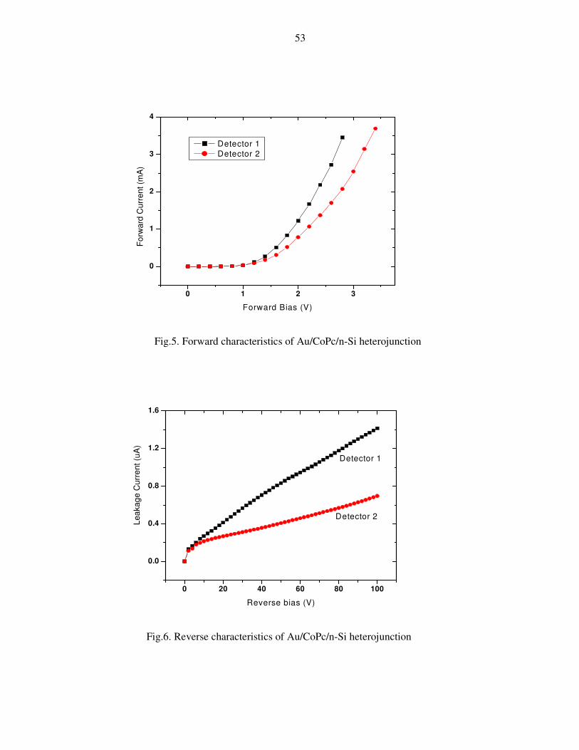
The forward and reverse I-V characteristics of detectors 1 & 2, just after their
fabrication are shown in Fig.5 & Fig.6 respectively. From their characteristics we can
say that both the detectors showed good diode behavior. The I-V curves of Detector1
got fitted with diode equation with diode ideality factor of n = 0.536 which is shown
in Fig.7. The I-t characteristics i.e. variation of reverse leakage current with time
(elapsed) for a fixed value of applied reverse voltage (40 V) for both Detector1 & 2
are plotted in Fig.8. It is observed that the leakage behaviors of both the detectors are
quite stable. Leakage current through Detector1 is almost double than that of
Detector2 for a given applied bias.
53
0 1 2 3
0
1
2
3
4
Fo
rward
Curr
en
t (m
A)
Forward Bias (V)
Detector 1
Detector 2
Fig.5. Forward characteristics of Au/CoPc/n-Si heterojunction
0 20 40 60 80 100
0.0
0.4
0.8
1.2
1.6
Detector 1
Detector 2
Lea
ka
ge C
urr
ent (u
A)
Reverse bias (V)
Fig.6. Reverse characteristics of Au/CoPc/n-Si heterojunction

54
-20 0 20 40 60 80 100
-3.5
-3.0
-2.5
-2.0
-1.5
-1.0
-0.5
0.0
0.5
n = 0.536
Cu
rrent
(mA
)
Bias (V)
Fig.7. Determination of Diode Ideality Factor
0 50 100 150 200
0.5
0.6
0.7
0.8
0.9
At Applied Reverse Bias = 40 V
Detector 2
Detector 1
Leakage C
urr
ent ( µµ µµ
A)
Time (s)
Fig.8. I-t characteristics for Au/CoPc/ n-Si heterojunction

55
Performances of both the detectors (i.e. Detector1 & Detector2) were studied over a
longer period of time (15 Months) to get information about their ‘long term
performance’. Fig.9 (a) and (b) indicate the long term performance with regard to
forward characteristics for Detector1 and Detector2 respectively. From the graphs
marked “15 Months after fabrication” pertaining to both the detectors (i.e. Detector1
& 2), it is seen that the kink in the forward current (where it starts rising exponentially)
shifts to a at a higher value of forward bias which may be due to aging of these
detectors in a similar fashion to what has been already described for CuPc/n-Si
heterojunction detectors above [31]. Actually there are two junctions, one at Au/CoPc
which is forward biased and the other one at Al/n-Si junction. So when the detector
was forward biased, though the Au/CoPc junction was forward biased, the weaker
junction formed due to aging of the detector (i.e. Al/n-Si junction formed due to aging)
was reverse biased. When the bias was increased, at certain higher value of voltage,
the device started conducting.
0 1 2 3
0
1
2
3
4
Forward characteristics of Detector 1
Fo
rward
Cu
rren
t (m
A)
Forward Bias (Volts)
As-prepared
15 Months after fabrication
Fig.9(a). Long term performance of Detector1 for forward characteristics

56
0 1 2 3 4 5
0
1
2
3
4
Forward I-V characteristics
of Detector 2
Fo
rward
Cu
rren
t (m
A)
Forward Bias (Volts)
As-prepared
15 Months after fabrication
Fig.9(b). Long term performance of Detector2 for forward characteristics
Fig.10 (a) and (b) show the ‘long term performance’ of Detector1 & 2 with respect to
their reverse characteristics. The result reveals only marginal increase in leakage
current over a period of 15 months. Degradation of epoxy during the period of 15
0 20 40 60 80 100
0.0
0.4
0.8
1.2
1.6
Reverse characteristics of Detector 1
Leakag
e C
urr
en
t (u
A)
Reverse Bias (V)
As-prepared
15 Months after fabrication
Fig.10(a). Long term performance of Detector1 with respect to
reverse characteristics

57
0 20 40 60 80 100
0.0
0.2
0.4
0.6
0.8
Reverse characteristics of Detector 2L
eakag
e C
urr
en
t (u
A)
Reverse Bias (V)
As-prepared
15 Months after fabrication
Fig.10(b). Long term performance of Detector2 with respect to
reverse characteristics
months may be the primary reason for such marginal increase in leakage current. But
only a marginal increase in leakage current over a time gap of 15 months indicates
about good stability of the fabricated detectors. For alpha particle spectra, both the
detectors (i.e. Detector1 & 2) placed under an alpha particle source (one detector at a
time) of 241
Am – 239
Pu inside a vacuum chamber with vacuum of ~10-3
Torr. The
distance between the source and the detector was maintained at 20 mm. These
detectors could be operated smoothly up to a reverse bias of 500 V (applied through a
load of 110 MΩ). The alpha spectroscopic measurements were carried out for both the
detectors (Detector1 & 2) and the spectra corresponding to optimum resolution,
studied just after fabrication as well as after a gap of 15 months for detectors 1 & 2 are
shown in Figs.11 and 12 respectively. The energy resolution of Detector1 (41 keV) is

58
better than that of Detector2 (45 keV) though the active area of Detector2 (180 mm2)
is less than that of Detector1 (260 mm2). This may be due to the double thickness of
CoPc layer which might have created thicker dead layer for impinging alpha particles.
Though the energy resolution was remained almost same for Detector1, it got
decreased for Detector2 over a period of 15 months. To conclude, one can say that the
detector fabricated with 100 nm CoPc, can be produced by simple fabrication method
and offers stable performance over a period of 15 months. The graphs indicating the
variation of energy resolution with reverse bias voltage for Detector1 & 2 is
presented in Fig.13.
640 680 720 760 800 840 880 920 960
0
1000
2000
3000
4000 CoPc/n-Si Detector 1
(Alpha Spectrum)
Energy Resolution =
41.25 keV
Energy Resolution =
44.69 keV
FWHM=6.5 Channels
FWHM=7 Channels
Co
un
ts
Channel Number
As-prepared
After 15 Months from fabrication
Fig.11.Alpha spectra of detector1 (energy resolution of 41.25 keV is
obtained corresponding to Am-peak of energy 5.48 MeV).

59
520 560 600 640 680 720 760
0
500
1000
1500
2000 CoPc/n-Si Detector 2
(Alpha Spectrum)
Energy Resolution =
64 keVEnergy Resolution =
45 keV
FWHM = 7 ChannelsFWHM = 6 Channels
Cou
nts
Channel Number
As-prepared
After 15 Months from fabrication
Fig.12.Alpha spectra of detector2 (energy resolution of 45 keV is obtained corresponding to Am-peak of energy 5.48 MeV)
100 200 300 400 500 600
40
45
50
55
60
65
70
75
Detector 1
Detector 2
En
erg
y r
eso
lutio
n (
ke
V)
Reverse Bias (V)
Fig.13. Variation of energy resolution with reverse bias

60
It is observed from these plots that the energy resolution improves with increase in
reverse bias initially but after reaching the optimum value, subsequent increase in
reverse bias causes deterioration of energy resolution. It can be explained as, at lower
reverse voltage, the collection of the generated charge, in the active volume of the
detector was incomplete. So there is improvement in energy resolution with increase
in reverse voltage. But once all the generated charge got collected, further increase in
reverse bias will augment the leakage current in the device which in turn deteriorates
its energy resolution.
2.4 CONCLUSION
In this chapter we have discussed the modification of silicon surface barrier detectors
to MPc/Si heterojunctions using CoPc (which is an organic thin film) as an active
layer. Two film thicknesses have been tried to investigate the influence of organic
active layer thickness in reducing the leakage current. It was observed that the leakage
behavior is better than conventional surface barrier detectors with 100 nm thick CoPc
layer. Long term stability studies over a period of 15 months also suggested stability
and reliability of this new heterojunction device.

61
__________________________________
Chapter 3
SILICON SURFACE BARRIER
DETECTORS USING
ORGANIC/INORGANIC THIN FILMS AS
PASSIVATION LAYER
_____________________________________
3.1 Introduction
3.2 Materials/Methods adopted for Si-passivation
3.2.1 Silicon dioxide passivated delta E detectors
3.2.2 Development of epoxy passivated rugged silicon surface barrier detector
3.2.3 Junction edge passivation of silicon surface barrier detectors by tin
oxide layer formed as a result of thermal decomposition of Amine based
organic films deposited by L-B technique
3.2.4 Junction edge passivation of Silicon surface barrier detectors by
hydrogenated amorphous silicon layer
3.3 Conclusion

62
3.1 INTRODUCTION
One of the major problem areas faced by a detector developer is the highly active
nature of silicon surface. Passivation basically means the junction electrical properties
are not significantly degraded at the surface compared to their bulk properties. It is
now very much important to concentrate on the following data pertaining to silicon:
For silicon: No. of atoms/cc = 5×10²²
Hence number of atoms/cm.2 = (5×10²² )2/3 = 1.85×10¹⁵
So the no. of surface states = 1.85 ×1015
× 1-2 (No. of broken bonds)
= 2 to 4 times 1015/cm2
So the number of surface states is quite high which gives rise to larger value of
leakage current. So silicon surface needs passivation to bring down surface states to ~
1011 /cm2. Various materials have been explored to passivate Silicon surface. Some of
them are well established and are in regular use to fabricate silicon detectors e.g.
amine-based epoxy (organic material) to fabricate silicon surface barrier detectors and
silicon dioxide film (inorganic material) on silicon to fabricate diffused junction/
Passivated Ion-implanted Planar Silicon (PIPS) detectors etc. Now in the case of
silicon surface barrier detectors, epoxy gets deteriorated with time and accordingly
detector performance too gets deteriorated. In the case of diffused junction/(PIPS)
detectors, the passivating oxide layer won’t deteriorate with time but still some
problem remains. PIPS detectors [43-44] are having lesser dead layers as compared to
diffused junction detectors and are known for their long term stability. Unlike diffused
junction detectors, the junction depth can be accurately controlled by choosing
appropriate implantation energy for PIPS detectors and its fabrication involves low

63
temperature processes. But to fabricate PIPS, elaborate laboratory arrangement is
required. Typical configuration of a PIPS detector is as given in Fig.1 and its
fabrication steps are shown in Fig.2(a) &2(b) respectively. On the contrary fabrication
of surface barrier detectors requires very simple set-up.
Fig.1. PIPS detector configuration
Fig.2(a) Initial fabrication steps for PIPS detector [1]

64
Fig.2(b) Remaining fabrication steps for PIPS detector [1]
Now in the case of surface barrier detectors, replacing epoxy by SiO2 at the edge will
improve its long term stability. In partially depleted E-type surface barrier detectors,
replacing epoxy with SiO2 is implemented well by detector manufacturers and is also
reported in literature. But it is still not popular and not implemented in the cases of
very thin (10 – 30 µm), standalone and fully depleted ∆E-type detectors. This is due to
the fact that, heating such thin samples of silicon to 1000-1200˚C to grow SiO2 on it is
extremely difficult to achieve and these samples are more vulnerable to breakage due
to thermal stress at this high temperature. But there is another method to develop
oxide-passivated fully depleted ∆E-type detectors. In this method, one can start with
growing SiO2 on a thick sample and subsequently thinned down this sample to the
desired thickness. This method was utilized to develop few prototype oxide passivated
delta E detectors and it is described at length in the next section. Another problem

65
encountered in our laboratory is that the epoxy passivated surface barrier detectors are
not rugged due to poor adhesion of thermally evaporated gold film on n-silicon
surface. To overcome this, few detectors were fabricated using sputtered gold film on
silicon in place of thermally evaporated gold film to make them rugged. This is also
described in the next section.
It is well known that organic epoxy passivation of silicon surface can be done
by utilizing two-component epoxy. In order to cure the epoxy resin properly, one
needs to add right quantity of amine-based hardener. This results in very low leakage
current and stable detector performance. This prompts one to make use of amine-
based organic thin films as well either as passivation layer or it can behave as an
organic route to end up with an appropriate passivation layer. With this motivation, a
new material has also been explored to study edge-passivation of silicon surface
barrier detectors. This new material is tin oxide film and was formed as a result of
decomposition of an amine based L-B film [Octa Decyl Amine (ODA) – Stannate
complex] by heating it to a moderate temperature (i.e. by organic route). Initially Octa
Decyl Amine-Stannate Complex was deposited on Silicon wafer with the help of L-B
deposition technique. Subsequently the silicon wafer was heated in a furnace in
presence of air at a relatively low temperature (~ 600ºC). This heating causes
decomposition of L-B layer to form SnO2 film on silicon. This tin oxide contains
SnO2 nano-particles. This film of tin oxide offers very high resistance as it behaves
like a depletion layer. Details of fabrication and test results of these detectors are
described in the next section.

66
3.2 MATERIALS/ METHODS ADOPTED FOR Si-PASSIVATION
3.2.1 Silicon dioxide passivated delta E detectors
3.2.1.1 Experimental: Thin and fully depleted delta E detectors are very much useful
for many applications e.g. particle identification measurements and heavy ion
spectroscopy [45]. These detectors are Au/n-Si Schottky barrier detectors with their
junction edges passivated by organic epoxy. Fabrication of these detectors are quite
difficult because of the following two major factors viz. (a) device breakage due to
brittleness of thin silicon and (b) difficulty in achieving desired thickness uniformity.
In an oxide passivated thin detector, the edge of the thin silicon wafer is
covered by SiO2 layer in place of organic epoxy (which is used in the case of epoxy
passivated thin detectors). This was achieved by oxidation of thicker (greater than 500
micron) Silicon sample, followed by thinning, removal of SiO2 layer from all sides of
the sample except the radiation-entry side and finally opening a window there at the
centre. To start with, an n-type Si-wafer of 1″ diameter, of nearly 800 µm thickness,
11 kΩ-cm resistivity and oxide layer on all sides of 0.7 µm thickness was taken as the
starting material. The wafer was thinned to 30 µm (approx.) keeping the oxide layer
only on the radiation-entry side with the help of in-house thinning technique which
involves following four steps:
Step 1: Lapping of thick silicon samples was carried out in a lapping
machine ( Make: M/s Speedfam, Japan ) to bring down the sample thickness up to
200 µm. The rotational speed of the lap plate was kept at 35 rpm. The slurry used,
was made up of a mixture of 20 µm grain size powder and lapping oil.

67
Step 2: Preparation of samples of uniform thickness of 100 µm ( with a thickness
variation of ± 8 to 10 µm for samples of 1 inch diameter ) has been carried out using
a lapping fixture ( Make: M/s Lapmaster, USA ). The lapping fixture contains
three adjustable screws ( each screw provided with a diamond tip ). Height of the
screw tips from crystal mounting surface have been set at 100 µm with the help
of the angular scale attached to each screw ( coarse adjustment ) and dial gauge ( fine
adjustment ). Then by lapping the crystals mounted on this fixture (one crystal at a
time), the thickness of the wafers was brought down to 100 µm.
Step 3: Etching/chemical polishing of the 100 µm thick samples was performed to
bring the thickness down to 50 µm using 6:1:1 volumetric mixture of
HNO3:HF:CH3COOH (etching solution of etch rate ∼ 10 µm/minute).
Step 4: Final etching of ∼ 50 µm samples is carried out to bring down the
thickness below 25 µm using HNO3 : HF :: 20:1 etchant ( etch rate ∼ 3
µm/minute ).
Two 30 micron thick samples, thus prepared and window opened at the centre of the
oxide layer were fixed on ceramic mounts. Then a thin gold layer of 20 nm was
deposited onto the side having the oxide layer at the edge. On the backside, ohmic
aluminum contact of 200 nm was deposited by vacuum evaporation at 10-6 Torr
pressure. The ceramic mounts were held in transmission type metallic containers
provided with microdot connectors. The results presented hereafter were obtained
from the better performing detector. The detector is having active area of 95 (~11 mm
dia.) mm2. The photograph of the thinned sample is shown in Fig. 3 (a). Thickness
variation within ± 2 µm was measured in sample area of 5-6 mm diameter.

68
Fig.3. Photographs of different fabrication process steps of the ultrathin oxide-
passivated silicon surface barrier detectors: (a) ultrathin (30µm) oxidized Si wafer; (b)
oxide is etched out from the center; (c) final assembly of the detector after Au
metallization
3.2.1.2 Evaluation of results & Discussion: The detector was tested for its I-V
characteristics and alpha spectrum. The reverse characteristics of the detector are
shown in Fig.4. For charged particle detection, the detector was exposed to α-particles
from dual source (241Am – 239Pu). Alpha spectrum of the detector is shown in Fig.5.

69
0.0 0.5 1.0 1.5 2.010
-9
10-8
10-7
10-6
10-5
Le
ak
ag
e C
urr
en
t (A
)
Reverse bias (V)
Fig. 4. Reverse characteristics of the detector (The dotted line
indicates that a leakage current of >2µA occurs at >1.1 V).
360 380 400 420 440
0
50
100
150
Am Peak
Pu Peak
Co
un
ts
Channel Number
Fig.5. The Alpha spectrum obtained from the detector.

70
So the fabrication of thin (≤ 50 µm) of fully depleted silicon surface barrier
detector with its edges passivated with thermally grown SiO2 has been carried out
successfully. The detector exhibited leakage current of 2 µA for an applied reverse
bias of 1.1 V. It could also resolve Am and Pu peaks. Though the reverse
characteristics and alpha spectrum of these detectors are comparable with our own
standard detectors with edge passivation done by epoxy, these detectors promise
durability because of silicon dioxide passivation. Better quality of oxide as a starting
material may improve the leakage behavior and breakdown voltage further of these
devices. This work was presented and published in DAE symposium on nuclear
physics (2013) [46].
3.2.2 Development of epoxy passivated rugged silicon surface barrier detectors
3.2.2.1 Experimental: Detection and measurement of low energy nuclear particles
and fission fragments are carried out mainly by surface barrier detectors. There are
numerous fields where these detectors find their applications such as nuclear reaction,
isotope identification, space research, biology and radiation dosimetry etc. Surface
barrier detectors are actually based on the formation of Schottky barriers at
metal/doped-semiconductor interface and various researchers have reported about this
work [47-53]. As fabrication of these detectors, involves thermal evaporation of thin
gold film (~ 20 nm) onto n-Si wafer and its adherence with silicon is poor, these
detectors are highly vulnerable to damage and once damaged they automatically starts
malfunctioning. In literature, there is mention about various thin film deposition
techniques viz. electro- deposition, sputtering of gold etc. As requirement of wet
surface is a pre-requisite for electro-deposition, it is not suitable for detector
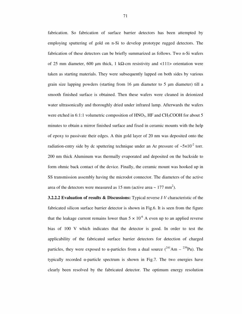
71
fabrication. So fabrication of surface barrier detectors has been attempted by
employing sputtering of gold on n-Si to develop prototype rugged detectors. The
fabrication of these detectors can be briefly summarized as follows. Two n-Si wafers
of 25 mm diameter, 600 µm thick, 1 kΩ-cm resistivity and <111> orientation were
taken as starting materials. They were subsequently lapped on both sides by various
grain size lapping powders (starting from 16 µm diameter to 5 µm diameter) till a
smooth finished surface is obtained. Then these wafers were cleaned in deionized
water ultrasonically and thoroughly dried under infrared lamp. Afterwards the wafers
were etched in 6:1:1 volumetric composition of HNO3, HF and CH3COOH for about 5
minutes to obtain a mirror finished surface and fixed in ceramic mounts with the help
of epoxy to passivate their edges. A thin gold layer of 20 nm was deposited onto the
radiation-entry side by dc sputtering technique under an Ar pressure of ~5×10⁻² torr.
200 nm thick Aluminum was thermally evaporated and deposited on the backside to
form ohmic back contact of the device. Finally, the ceramic mount was hooked up in
SS transmission assembly having the microdot connector. The diameters of the active
area of the detectors were measured as 15 mm (active area ~ 177 mm2).
3.2.2.2 Evaluation of results & Discussions: Typical reverse I-V characteristic of the
fabricated silicon surface barrier detector is shown in Fig.6. It is seen from the figure
that the leakage current remains lower than 5 × 10⁻⁶ A even up to an applied reverse
bias of 100 V which indicates that the detector is good. In order to test the
applicability of the fabricated surface barrier detectors for detection of charged
particles, they were exposed to α-particles from a dual source (241
Am – 239
Pu). The
typically recorded α-particle spectrum is shown in Fig.7. The two energies have
clearly been resolved by the fabricated detector. The optimum energy resolution

72
(FWHM) of 70 keV was obtained for the detector when a reverse voltage of 400V was
applied through a preamplifier of 110 MΩ load resistance and the measured leakage
current was 3.34 µA. The measured energy resolution was slightly poorer as compared
to our own detectors fabricated by vacuum thermal evaporation i.e. the energy
resolution is compromised at the cost of better ruggedness. The higher energy of the
gold atoms during sputtering could have caused little damage to the silicon surface
which in turn made the resolution poorer. The energy of gold atoms can be fine tuned
by varying the pressure of the Argon gas during sputtering. Making some more
detectors by varying pressure of Argon, one can optimize the detector performance.
0 20 40 60 80 100
0.0
1.0x10⁻⁶
2.0x10⁻⁶
3.0x10⁻⁶
4.0x10⁻⁶
5.0x10⁻⁶
6.0x10⁻⁶
Le
ak
ag
e C
urr
en
t (A
)
Reverse bias (V)
Fig.6. Reverse I-V characteristic of the gold sputtered surface barrier detector.
The adhesion of sputtered gold film on n-Si was evaluated by two methods: (a) At
first the adhesion was tested as per ASTM standard by pasting special adhesive tape
3M Scotch on gold film and subsequent withdrawal of the tape witnessed no damage
73
300 320 340 360 380 400
0.0
5.0x10²
1.0x10³
1.5x10³
2.0x10³
Am peak
Pu Peak
Co
un
ts
Channel No.
Fig.7. Alpha spectrum of the gold sputtered surface barrier detector.
to the film and (b) Secondly, the gold film was gently scrubbed using a tissue paper.
It was observed that, unlike the thermally evaporated gold films, the sputtered gold
films do not peel off and thus suggesting better adhesion. The higher kinetic energy
of the gold atoms during deposition by sputtering may be the reason for this better
adhesion. So the fabrication of rugged surface barrier detector has been demonstrated
and the detector could resolve the energies of the α-particles from a dual source
(241Am – 239Pu). This entire work has been presented and published in 31st IARP
National Conference on Advances in Radiation Measurement Systems and
Techniques [54].

74
3.2.3 Junction edge passivation of silicon surface barrier detectors by tin oxide
layer formed as a result of thermal decomposition of Amine based organic films
deposited by L-B technique
3.2.3.1 Experimental: To fabricate detectors using this passivation method, p-type
silicon slices of 2 inches diameter, 1 mm thickness and 8 kΩ-cm resistivity were taken
as starting materials. They were subsequently lapped with various grain size (starting
with highest available grain size and completed with lowest available grain size)
carborandom/alumina powders. Then thick layers (~ 500 nm) of gold were deposited
on the backside of the lapped wafers using electro-less plating and the gold layers
were masked properly by black-wax before proceeding for chemical polishing.
Afterwards chemical polishing was carried out by dipping the mechanically-polished
wafers (one at a time) into an etchant solution composed of 6:1:1 volumetric mixture
of HNO3:HF:CH3COOH for 5 minutes. Removing the black wax from the back side
resulted in front-side polished Si-slices with their backside covered with gold. The
chemically polished front sides of the wafers were then partially covered by tape (as
mask) of 38 mm diameter, covering the central part leaving the peripheral annular
region (at the edge) open. Tape was also utilized to cover their entire backside gold
layer. Multilayer L-B films of Octa Decyle Amine (ODA) – Stannate complex of 95
to 100 layers were deposited on the entire surfaces of both sides of these already
masked silicon wafers. After deposition, the masking-tapes were removed and the
covered areas under the masks were thoroughly cleaned with trichloroethylene (which
actually degreased the Si-surfaces and also made it free from various other
organic/inorganic contaminants). After removal of tapes, the deposited L-B film
remained only at the annular area (at the edge) on the front side. In the next step the

75
Si-samples were kept inside a pre-cleaned quartz tube (one sample at a time) and
placed the quartz tube loaded with the sample inside a furnace. Subsequently, the
samples were heated with a ramping rate of ~ 5˚C/min to attain 600˚C (in air) in two
hours and remain there for three hours (i.e. dwell time). This heating results in
decomposition of multilayer L-B film to form high resistive SnO2 film at the edges of
the wafers. Growing SnO2 film (ρ ≈ 10-20 MΩ-cm) on a Silicon wafer is a new as
well as simpler technique [26 – 27] and has been explored to study passivation of
Silicon detectors. Thermal evaporation of Aluminum was carried out to deposit Al-
film of thickness 40 µg/cm2, on to the central portion, at the front-side of the Si-
wafer, covering partly the SnO2 layer. Gold film of thickness 40 µg/cm
2 was
evaporated on the rear side as an Ohmic contact.
3.2.3.2 Evaluation of results and Discussions: The fabricated detectors were
evaluated with the help of their I-V characteristics measurement (both forward and
reverse) and alpha spectroscopic study. The front and backside of one of the
fabricated detectors prior to mounting and encapsulation are shown in Fig.8.
Fig.8. Photographs of front and backside of an un-mounted detector.
Forward and reverse I-V characteristics of the best performing detector are shown in
Fig.9 and 10 respectively. Larger active area of the detector (diameter of the active
area ~ 38 mm) gives rise to larger value of leakage current. Both “As-prepared” and

76
0.0 0.5 1.0 1.5 2.0 2.5 3.0-0.5
0.0
0.5
1.0
1.5
2.0
2.5
3.0
3.5
4.0
As-Prepared
~ 30 Months LaterFo
rward
Cu
rren
t (m
A)
Forward Bias (Volts)
Fig.9. Forward characteristics of the detector.
0 20 40 60 80 100
0
50
100
150
200
250
300
~30 Months later
As-PreparedLeakag
e C
urr
en
t (u
A)
Reverse Bias (Volts)
Fig.10. Reverse characteristics of the detector.

77
0 10 20 30 40 50
-2
0
2
4
6
8
10
12
14
16
18
20
22
24
SnO2 passivated detector
Detector without passivation
Leakag
e C
urr
en
t (u
A)
Reverse Bias (V)
Fig.11. Comparative reverse I-V characteristics of detector with/without
passivation.
“30 Months later” characteristics were measured and incorporated in forward as well
as reverse characteristics in order to have an idea about long term performance. The
effectiveness of the tin oxide passivating layer was verified by comparing the reverse
I-V characteristics of the detector having tin oxide passivating layer with the reverse
characteristics of another detector having no passivating layer [55]. This comparison
is shown in Fig.11 which indicates that the SnO2 passivation layer helps in reducing
the leakage current. The alpha spectrum of the detector, obtained using 241
Am-239
Pu
alpha source, by keeping the source and the detector 5 cm apart and under rotary
vacuum (~10-3
Torr), is shown in Fig.12.

78
280 300 320 340 360 380 400 420 440 460 480
0
100
200
300
400
500
600
No
. o
f co
un
ts
Channel No.
Fig.12. Alpha spectrum of the detector.
As the active area of the detector is very large, its capacitance is also very high.
Higher the value of capacitance, higher will be the noise generation in the detector.
This in turn affected the energy resolution thereby not resolving Am and Pu-peaks.
But the detector can still work as a solid state counter. In order to have a better idea
about the surface morphology of the newly grown tin oxide layer, SEM images of its
surface were taken for two different scales and are shown in Fig.13. The SEM image
corresponding to 100 nm scale is presented in the inset and the main image was
acquired by keeping the scale set at 200 nm. SEM Micrograph reveals close packed
distribution of SnO2 nano-crystals of size about 50 nm.

79
Fig.13. SEM Image of SnO2 surface.
The EDS spectrum is measured in three different locations on the surface of the SnO2
layer and most detailed one is presented in Fig.14. EDS spectrum shows
predominantly the peaks corresponding to Sn and O in the newly formed SnO2 layer.
Also there is feeble presence of zinc as metallic impurity which might be responsible
for higher reverse leakage current.

80
Fig.14. EDS spectra of the SnO2 thin film prepared by LB method.
This entire work has been reported for publication in the journal “Bulletin of Material
Science” (Springer Publications), which subsequently got accepted.
3.2.4 Junction edge passivation of Silicon surface barrier detectors by
hydrogenated amorphous silicon layer
It is reported in the literature that Hydrogenated amorphous silicon (a-Si:H), can be
used as an excellent passivant for crystalline silicon (c-Si) p-n junctions [28].
Researchers have reported a two orders of magnitude reduction in reverse leakage
current from that of a typical thermal oxide passivated junction. This material has
been attempted to passivate the edge of silicon surface to fabricate silicon surface
barrier detector. Two n-type silicon wafers of 1 inch diameter, 4.5 kΩ-cm resistivity

81
and 1 mm thickness were taken as starting material. The front side (top
view) of the polished, edge-passivated and mounted silicon wafers, prior to taking
gold evaporation on it, is shown in Fig.15. Two surface barrier detectors were
fabricated with their edges passivated by hydrogenated amorphous silicon and tested
subsequently for I-V Characteristics. But their I-V didn’t show diode behavior as there
was hardly any difference between forward and reverse currents. Optimization in the
process to make hydrogenated amorphous silicon layer need to be done to get proper
results.
Fig.15. Photograph of the front side (Top view) of a-Si:H passivated silicon surface.
3.3 CONCLUSION
This chapter describes the fabrication, characterization of SSB detectors for alpha
particle detection using two different edge passivations; (a) thermally grown SiO2 and
(b) SnO2 thin films prepared by LB method. Edge passivation by SiO2 is reliable in
terms of leakage current and energy resolution for thicker silicon substrates, however,

82
for thin silicon detectors chances of breaking of the substrate is higher. Passivation by
SnO2 thin films is perhaps more appropriate for thinner silicon substrates, however,
further studies are required to improve the energy resolution by using smaller active
area of the detectors as in the case of detectors with SiO2 edge passivation. The
ruggedness of the gold contact of Au/n-Si junction has been studied by depositing
gold contacts using sputtering. It was observed that sputtered gold films gave better
ruggedness for the SSB detectors.
83
_____________________________________
Chapter 4
DEVELOPMENT OF IMPROVED
SURFACE BARRIER DETECTORS BY
EMPLOYING ARGON COLD PLASMA
ASSISTED SILICON SURFACE
CLEANING
_____________________________________
4.1 Introduction
4.2 Experimental
4.3 Results and discussions
4.4 Conclusion

84
4.1 INTRODUCTION
Silicon is an important material whose properties have been exhaustively studied
[56]. It continues to remain a material of choice for large scale use in device
fabrication, which includes integrated circuits, micro-electro-mechanical systems
(MEMS), solar cells, nuclear radiation detectors etc. The silicon surface plays an
important as well as a crucial role in many process steps used to fabricate these
devices, especially silicon surface barrier detectors. The silicon surface needs to be
exhaustively cleaned prior to fabrication of these detectors. The conventional way of
cleaning silicon surface by using specific organic and inorganic solvents [57-58] is
time consuming and tedious, while the solvents used are toxic and are also responsible
for environmental pollution. Besides, for solar cells, produced from single crystal,
polycrystalline, or amorphous silicon, the respective surface must be carefully cleaned
either before an oxide mask layer is allowed to grow, or prior to deposition of an anti-
reflection coating [59]. The usage of atmospheric pressure oxygen plasma provides a
convenient, in-line treatment process for cleaning as well as activating silicon surfaces
[59-61]. Though surface modification of silicon using plasma has been reported by
many researchers, no information is available in the literature about how this surface
cleaning/modification can influence the performance of silicon based nuclear radiation
detectors. It is observed in semiconductor industry that the properties of
surface/interface of silicon based layers play a key role in fabrication of devices.
Different applications require different properties of such surface/interface layers. It is
also mentioned in literature that the modification of surface properties of silicon based
layers involves either toxic processes or is highly energy consuming [62-64]. However
the use of plasma technology provides an environmentally acceptable and cheaper

85
alternative. Though the low pressure plasma technology is highly efficient and widely
used in the industry, efforts are on to replace it by atmospheric pressure plasma [62].
Plasma activation of silicon surface for self-assembly, in an attempt to optimize and
simplify the formation of hydrophilic silicon surface, is a relatively safer and simpler
route which replaces the conventional means to form hydrophilic silicon surface with
the help of corrosive and harmful piranha solution [65]. Researchers have also
separately studied plasma oxidation of silicon exhaustively [66-67]. However, very
little information exists in the literature on the possibility of technical use of cold
plasma for nuclear detector fabrications. The cold plasma facility used in the present
study is a compact and low cost table-top unit and does not require any elaborate
laboratory arrangements. The design, fabrication, and usage details of this low cost,
table-top equipment have been published recently [68]. Moreover, by employing this
equipment, usage of solvents could be avoided. So this method of cleaning silicon
surface has simplified the fabrication of surface barrier detectors, over and above the
inherent benefit of choosing simple surface barrier fabrication technique as compared
to elaborate arrangements of ion-implantation/diffusion techniques.
4.2 EXPERIMENTAL
Fabrication of surface barrier detectors using silicon slices cleaned by cold plasma
was carried out as follows:
At first, single crystal silicon slices (n-type, ~14.9 kΩ-cm resistivity, 34.3 mm
diameter and 1 mm thickness) were cut from ingot with the help of diamond wheel in
a wafer cutting machine. Then these slices were mechanically lapped using
carborandum/alumina powders and then chemically polished on both sides in 6:1:1

86
volumetric composition of HNO3:HF:CH3COOH. Before carrying out cold plasma
assisted cleaning of the etched silicon surface, the etched wafers were cleaned by
dipping them in de-ionized water in a beaker and vibrating the beaker ultrasonically.
Subsequently the slices were dried by keeping them under an infrared lamp. Now the
slices are ready for exposure to cold plasma. Four wafers were cleaned using cold
plasma under four different conditions. First wafer was exposed to the cold plasma
formed by Argon gas (Argon gas purity 99.999% and flow rate maintained at 2.8
lit/min) for 3 minutes, while the second wafer was exposed to cold plasma formed by
a mixture of Argon and Ambient Laboratory Air (90% Argon and 10% Air, Argon
flow rate was 2.8 lit/min and Air flow rate was ~300 ml/min), also for 3 minutes. The
third wafer was first exposed for 3 minutes to cold plasma of Argon and Air (90%
Argon and 10% Air, Argon flow rate was 2.8 lit/min and Air flow rate was ~300
ml/min) similar to the second wafer, followed by an additional exposure for 2 minutes
to cold plasma formed by a gas mixture of Ar and moist Air [Air was passed through
de-ionized water at room temperature (300 K) of 18 MΩ-cm resistivity using a
bubbler] (90 % Ar and 10% moist Air). Hence total time of exposure of this wafer to
plasma is 5 minutes. The fourth wafer was exposed to cold plasma of Ar and moist
Air (90% Ar and 10% moist Air) for 3 minutes. Hereafter the detectors fabricated out
of first, second, third and fourth wafers will be termed as D1, D2, D3 and D4
respectively. The plasma coming out of the flexible brush had a spot diameter of
approximately 3 mm [68]. It was fixed at a distance of 5mm over the wafer surface in
a Z-axis clamp, and the silicon wafer was made to glide underneath this tip in X-Y
directions by hand, mimicking a 2D plotter movement (or raster scanning), so that the

87
entire silicon surface could be scanned uniformly by the plasma tip within the preset
time duration. The four plasma exposure conditions are given in Table-I below:
TABLE - I
Detector
Plasma gas composition
Ar flow rate 2.8 lpm, Air flow rate 300mlpm
Duration of
exposure (min)
Optimum
energy resolution
(keV)
D1
Argon
3
α-peaks are not
well
resolved
D2 90% Ar + 10% Air 3 53
D3
90% Ar + 10% Air
and followed by 90% Ar + 10% moist
Air
3
2
(total 5)
97.77
D4
90% Ar + 10% moist Air
3
79.41
(This table is taken from our published paper: A. Ray et al 2018 JINST 13 P09019)
Then the samples were mounted on ceramic mount using organic epoxy [a mixture of
one drop epoxylite hardener No. 323 (obtained from M/s Epoxylite corporation,
U.S.A.) and five drops of vacuum pumped CIBA 230 Araldite epoxy resin (Make:
Hindustan CIBA-GEIGY Ltd. under license from CIBA-GEIGY AG, Basel,
Switzerland)]. Au of thickness ~ 40 µg/cm2 was deposited on radiation-entry side of
silicon wafer by thermal evaporation under high vacuum (~ 10-6
Torr). Ohmic Al
contacts of thickness ~ 40 µg/cm2 were also deposited on backside of the wafers. The
depositions were carried out at a substrate temperature of 300 K. In case of
conventional Au/n-Si surface barrier detectors, prior to depositing Au of 20 nm
thickness (~ 40 µg/cm2) on to the radiation-entry side of silicon wafer, the silicon
surface is cleaned by organic solvents and not by cold plasma [30]. So actually it is

88
the silicon surface cleaning process which differs. The evaluation of the fabricated
detectors was carried out by measuring current-voltage (I-V) characteristics (both
forward as well as reverse characteristics), measurement of detector response to α-
particles (i.e. measuring optimum alpha energy resolution) and also measuring the
variation of alpha energy resolution with reverse bias voltage. Measurement of I-V
characteristics under forward as well as reverse bias were carried out using Keithley
make programmable electrometer. Alpha spectra for the detectors were obtained using
241Am –
239Pu dual α-particle source and PC based multi-channel analyzer. The energy
resolutions of the detectors were measured as a function of reverse bias voltage (n-
silicon positive with respect to Au). For alpha particle spectroscopic measurements,
the source and the detector were placed in a vacuum chamber (at ~ 10-3 Torr) with a
separation of the order of the diameter of the detector.
4.3 RESULTS AND DISCUSSIONS
The schematic of the Au/n-Si surface barrier detector is shown in Fig.1 and the
photograph of the cold plasma facility which was utilized to clean silicon samples’
surfaces is given in Fig.2. The forward I-V curves of the four detectors are shown in
Fig.3 and the reverse I-V curves are shown in Fig.4. From the forward and reverse
characteristics we can say that all the detectors are showing very good diode
behaviour. The reverse leakage current obtained for D2 is lowest among all the four
detectors and it is also lower than that for best conventional Silicon Surface Barrier
(SSB) detector prepared in our laboratory previously [30]. The forward and reverse
I-V curves of D2 and the best SSB detector are shown in Fig.5 and Fig.6 respectively
purely for comparison purpose. The presence of reactive free radicals, e.g. H-atom,

89
•OH radical and HO2• radical (usually referred to as reactive oxygen species, or ROS)
and reactive nitrogen oxides, NO• and NO2• (generally referred to as reactive nitrogen
Fig.1. Schematic of Au/n-Si un-mounted surface barrier detector.
Fig.2. Cold Plasma Flexible Brush plume of Ar gas ~10 mm over aqueous sample in a
beaker, with 12.8 kVp−p applied voltage at Ar flow rate 10 ml .s−1 [68].

90
-0.2 0.0 0.2 0.4 0.6 0.8 1.0 1.2 1.4 1.6 1.8 2.0 2.2 2.4
-0.5
0.0
0.5
1.0
1.5
2.0
2.5
3.0
3.5
4.0
Forward Characteristics
of Plasma Cleaned Detectors
Fo
rward
Cu
rren
t (m
A)
Forward Bias (Volts)
D1
D2
D3
D4
Fig.3. Forward Characteristics of the four detectors D1, D2, D3 and D4.
Species, or RNS) in the plasma as reported in details in the literature [68], is
responsible for such behavior, as it quickly reacts with all sorts of organic surface
materials and oxidize them into carbon dioxide and water [68]. When plasma is
prepared from the gas mixture of Argon and moist air (as in the cases of D4 and D3),
the small amount of water molecules present in the moist air will react with NO• and
NO2• and form HNO3 in presence of O2. HNO3 is a strong acid as well as oxidizing
agent. Thus, it is expected to modify and etch the Si surface to some extent. As a
result of this, the leakage current of D4 is slightly higher than D2. Between D4 and
D3, D3 showed more leakage current. As a qualitative observation, we can say that
prior to fabricating D3, the Si- surface was under cold plasma for a longer time (5

91
0 20 40 60 80 100
-5
0
5
10
15
20
25
30
35
40
0 20 40 60 80 100
0.1
1
10
Reverse Characteristics of
Plasma cleaned Detectors
Leakag
e C
urr
en
t (u
A)
Reverse Bias (Volts)
Det.1
Det.2
Det.3
Det.4
Reverse Characteristics of
Plasma cleaned Detectors
Leakag
e C
urr
en
t (u
A)
Reverse Bias (Volts)
Det.1
Det.2
Det.3 Det.4
Fig.4. Reverse Characteristics of the four detectors D1, D2, D3 and D4.
minutes) than that for D4 (3 minutes). From the reverse characteristics, it is observed
that the leakage behavior of D2, D3 and D4 (Argon + Air cases) are closely spaced
lines which are wide apart from D1 (only Argon case). The reason for the higher
leakage current of D1 can be due to the presence of energetic ions such as Ar2•+
, Ar3•+
etc. in the plasma (when only argon cold plasma is used) which due to their heavy
mass as compared to Si, possibly damage the latter surface irreversibly [1]. But in the
cases of D2, D3 and D4, even though Argon is present in the plasma, due to the
presence of air/moist air, the possibility of creation of Ar2•+, Ar3
•+ ions becomes very
feeble.
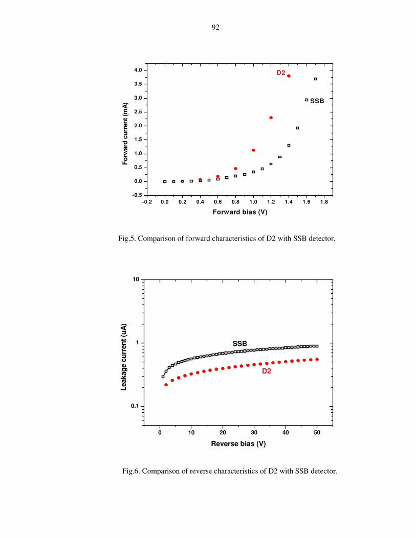
92
-0.2 0.0 0.2 0.4 0.6 0.8 1.0 1.2 1.4 1.6 1.8
-0.5
0.0
0.5
1.0
1.5
2.0
2.5
3.0
3.5
4.0
SSB
D2
Fo
rward
cu
rren
t (m
A)
Forward bias (V)
Fig.5. Comparison of forward characteristics of D2 with SSB detector.
0 10 20 30 40 50
0.1
1
10
SSB
D2
Leakag
e c
urr
en
t (u
A)
Reverse bias (V)
Fig.6. Comparison of reverse characteristics of D2 with SSB detector.

93
For charge particle detection, these detectors were exposed to α-particles from dual
source (241Am–239Pu), irradiating particles with energies of 5.48 and 5.15 MeV. The
detectors used for this measurement had an active area of ~250 mm2. During
measurements, both detector and source were placed in vacuum. Because of the higher
leakage current (as discussed above), D1 offered very poor resolution and it is almost
of no practical use as far as spectroscopic measurements are concerned. The best alpha
spectra obtained from D2, D3, D4 and the best prepared SSB in our laboratory are
shown in Fig.7, 8, 9 and 10 respectively. The variation of energy resolution for the
three detectors i.e. D2, D3 and D4 with reverse bias voltage i.e. alpha energy
resolution as a function of reverse bias voltage is plotted in Fig.11. In this figure, the
voltage shown is the total applied voltage to the device in series with a load resistance
of 110 MΩ.
700 750 800 850 900 950
0
1000
2000
3000
4000
5000
of 230.6 V across D2For applied reverse biasEnergy resolution = 53 keV
FWHM =
9 channels
Pu peak at
channel no.854
Am peak at
channel no.910
Co
un
ts
Channel Number
Fig.7. Best alpha spectrum obtained from D2 (energy resolution of 53 keV is obtained corresponding to Am-peak of energy 5.48 MeV).

94
280 300 320 340 360 380 400 420 440 460 480
0
1000
2000
3000
4000
5000
FWHM =
8.1 Channels
Energy resolution = 97.77 keV
For applied reverse bias of
47.8 Volts across D3
Pu Peak
(Channel No.412)
Am Peak
(Channel No.439)
Co
un
ts
Channel Number
Fig.8. Best alpha spectrum obtained from D3 (energy resolution of 97.77 keV is obtained corresponding to Am-peak of energy 5.48 MeV).
360 380 400 420 440 460 480 500 520 540
-500
0
500
1000
1500
2000
2500
3000
3500
Energy Resolution = 79.41 keV
for applied reverse bias of
64 Volts across D4.
FWHM =
7.46 Channels
Pu Peak
(Channel No.458)
Am Peak
(Channel No.489)
Co
un
ts
Channel Number
Fig.9. Best alpha spectrum obtained from D4 (energy resolution of 79.41 keV is obtained corresponding to Am-peak of energy 5.48 MeV).

95
600 650 700 750 800
0
200
400
600
50 keV
Pu peak
Am peak
Nu
mb
er
of
co
un
ts
Channel Number
Fig.10. Best alpha spectrum obtained from SSB (Energy Resolution=50 keV).
100 200 300 400 500 600 700
50
60
70
80
90
100
110
120
130
D2
D3
D4
En
erg
y R
eso
luti
on
(keV
)
Reverse Bias (Volts)
Fig.11. Variation of energy resolution with reverse bias voltage (as the leakage current
through D1 is quite high, it offered very poor resolution and hence omitted in this
figure).

96
This entire work is published in Journal of Instrumentation (JINST), IOP Publishing
(U.K.) [69].
4.4 CONCLUSION
Environment friendly and simple method of cleaning for silicon wafers using
cold plasma in place of conventional chemical cleaning has been tried. Four types of
cold plasma compositions (Argon, air, moisture) and plasma exposure durations have
been tried to evaluate the dependence of leakage current and energy resolution of the
detectors on plasma cleaning. From the study we can conclude that cleaning with only
Argon cold plasma is not very effective in terms of leakage current and energy
resolution. However, the leakage current of D2 is lowest among all the four detectors
fabricated and also lower compared to best conventional SSB detector fabricated in
our laboratory earlier. In the present study we have optimized the gas composition of
the cold plasma for best detector performance amongst “pure Argon (0% humidity),
Argon with pure Air (trace humidity) and Argon with moist Air (~10% humidity)”. In
order to get a qualitative idea, D3 was fabricated using longer exposure time. In this
case, the mixed exposure for D3 was conducted to check the effect of a sequential
protocol. Since the plasma plume formed out of pure Argon is exposed to open air,
there is a possibility that a trace amount of air and/or moisture may get added with that
Argon and their effects will be unavoidable. However continuous gas flow in all the
cases ensured that such effects remains minimal. Lastly, conducting experiment using
a single detector, fabricated out of each plasma condition, has produced results which

97
are indicative of the effect and more number of detectors from each category i.e. more
statistics are needed to make the results more conclusive.

98
_____________________________________
Chapter 5
PURELY ORGANIC RADIATION
SENSORS
_____________________________________
5.1 Introduction
5.2 Experimental
5.3 Results and discussions
5.4 Conclusion

99
5.1 INTRODUCTION
Detection of alpha particles, heavy ions etc. is an essential feature in various
nuclear physics experiments. For this purpose, solid state detectors and especially
silicon detectors are playing a leading role. Let us now switch our focus for the time
being from Nuclear Physics to Health Physics. We all know that the naturally
occurring radioactive materials (e.g. uranium, thorium and radon) and artificial
radioactive elements (e.g. plutonium and americium) are the emitters of alpha
particles and therefore some of them are very much in use to prepare alpha emitting
sources. These alpha particles may cause threat in case of being inhaled or ingested by
someone or even more dangerous in case they get absorbed in someone’s blood. In all
such cases, it may cause damage to body tissues and hence enhances the risk of being
affected by cancer. To be more specific, firstly the uranium mining waste and
secondly the concentrated natural radium generated while processing phosphate ore to
produce fertilizer, are the two major alpha emitters through which mankind is directly
getting exposed to alpha. So in order to prevent the environment from getting
contaminated, it is very much essential to detect the alpha particles in and around such
industries. To suit this stringent requirement, one must look for a sizable number of
flexible as well as portable alpha sensors. In this context, perhaps the development of
organic polymer based detectors would be best suited ones because of its capability to
be flexible, as well as portable. Also they can be prepared in large scale and that too at
a very low cost. There are certain properties of organic semiconductors which look
alike to those of inorganic semiconductors, like Silicon and Germanium and for this
very reason, one can think of treating them as a substitute for Silicon and Germanium
in many devices. Researchers are taking interest in this new as well as challenging

100
field primarily due to the relative simplicity of the technological implementation
promising substantial economical benefits and also side by side opening the scope for
getting new semiconductor products e.g. Organic FET, Organic LED, Organic
Photovoltaic devices etc. Owing to the differences in physical and chemical properties,
organic semiconductors could serve as a starting material for various new and
improved sensors and detectors [34]. Semiconducting organic material may be
subdivided into three categories viz. polymers, oligomers and small molecules
depending on the length of the molecular structure that sets mechanical, chemical and
electronic properties [70].
This chapter deals with the interaction of alpha particles with polymer material
(BoPET). The outcomes of such interactions were analyzed in detail as these
outcomes can be considered as the stepping stones towards the development of
polymer based detectors. Crystalline organic substance and non-crystalline materials,
e.g., plastics, suffer radiation effects through other mechanisms, chiefly the breaking
of chemical (covalent) bonds. The threshold energy for such breakage is also of the
order of 25 eV [71]. As exposure to ionizing radiation will break many bonds in
polymer material (also called radiation damage) it will cause generation of charge
carriers (e-h pairs). So by irradiating with ionizing radiations, it is expected that the
conductivities in polymer materials [e.g. Polyanilene, Biaxially Oriented Poly
Ethylene Terephthalate (BOPET) etc.] will be changed. This change in conductivity
was studied for alpha particles to carry out their detection. The results obtained for the
change in conductivity of BoPET film, due to its exposure to alpha particles, are being
reported in the subsequent section.

101
5.2 EXPERIMENTAL
BoPET film was developed in the mid-1950s, originally by DuPont, Imperial
Chemical Industries (ICI) and Hoechst. It is also called Bi-axially Oriented PET
where PET is called Poly Ethylene Terephthalate. The chemical structure of PET is
shown in Fig.1. A number of samples were made using thin sheet of BoPET and
Fig.1. Chemical structure of PET.
studied their current conducting behavior before and during exposure of the samples
to alpha particles. On each of these samples (i.e. on each small piece of thin BoPET
sheet of size 6mm × 2mm (approx.) which was mounted on a glass slide with the help
of epoxy) there are two closely separated (12 µm) and 30 nm thick gold pads
(deposited by physical vapour deposition). Electrical connection to the sample was
established with the help of two single strand wires, held by silver paste on the two
gold pads deposited on BoPET samples. In order to see the current vs. time behavior
(i.e. I-t characteristics), a fixed voltage in the range of 40V to 90V was applied
between the two pads and the current was measured over a period of 200-600 seconds.
Afterwards, an increase in this current was observed for the same applied bias across
the pads of the sample when it was exposed to 5 MeV alpha particles from 241Am –

102
239Pu source. Identical measurements were carried out with the help of samples
prepared out of BoPET sheet coated with gold nanoparticles. But no change in the
device current was witnessed before and during exposure of 5 MeV alpha particles.
Also some samples, comprising of larger separation (~ 330 µm) between the gold pads
on a bigger size (15 mm × 6 mm) of BoPET sheet, were prepared and similarly tested.
Extremely low value of current was observed and there was no change in the value of
current before and during exposure of 5 MeV alpha particles. The reason could be: the
charge carriers generated by the applied voltage and/or by radiation may get
recombined before reaching the respective contacts. An experiment was conducted by
exposing two BoPET samples (Size: 6 mm × 2 mm, Separation between two gold pad:
12 µm) periodically to an alpha source of higher activity (0.5 mCi), by placing the
source on the sample for some time, then withdrawing the source for some duration,
again placing the source on the sample for some time and so on. It was found that the
current also got increased and decreased periodically in the same fashion as the source
was placed and withdrawn. Keeping view of the results obtained from two samples,
the better result corresponding to a particular sample (Sample I), is presented in Fig.2
which shows the variation of current through the BOPET sample with time when it
was periodically exposed to 5 MeV alpha in air from a source of activity 0.5 mCi. An
increase in current of ~ 60 pA during alpha exposure as compared to its value before
exposure was observed. Typical values of current observed were 320 pA and 380 pA
with respect to ‘before exposure’ and ‘during exposure’ cases respectively for an
applied bias of 40 V. Subsequently, for testing the detector performance under
vacuum conditions (2nd experiment), one vacuum measurement set-up was developed
where an alpha source and another BoPET sample (Sample II) [size: 6 mm × 2 mm,

103
Separation between two gold pad: 12 µm] can be placed inside a vacuum chamber and
the chamber can be kept under rotary vacuum (~ 10-3 Torr). At first the device current
was measured in air for an applied bias of 90 V across the sample without exposing it
to alpha particles (by placing the sample inside the chamber which was kept at
atmospheric pressure by not doing any evacuation.
0 100 200 300 4000.30
0.32
0.34
0.36
0.38
0.40
0.42
0.44
Cu
rre
nt
(nA
)
Time (s)
αe
xp
osu
re o
n
αe
xp
osu
re o
ff
Fig.2. BOPET sample was periodically exposed to 5 MeV alpha in air from a source
of activity 0.5 mCi and the device current vs. time was recorded for an applied fixed
bias of 40V across the sample (Sample I).

104
Fig.3 shows the variation of device current, which is plotted against time-elapsed to
obtain the steady-state value of the device current for a particular value of the bias
voltage (90 V). Then the sample and the alpha source were kept under vacuum and a
clear jump of device current was observed (from 3.44 pA to 25.1 pA by using an
alpha source of lower activity ~ micro-Curie (12108.19±32.79 Bq) and from 2.68 pA
to 21.5 pA by using an alpha source of still lower activity of ~ nano-Curie (36.63 Bq)
as shown in Fig.4 for an applied bias of 90 V across the sample.
5.3 RESULTS AND DISCUSSIONS
It was observed that when the experiment was conducted in air, the base current (i.e.
current measured in absence of alpha exposure) was more for the experiment
corresponding to Fig.2 than that for the experiment corresponding to Fig.3. The reason
can be attributed as follows:
(a) In the case of Fig.2, there was a surface adsorbed layer (from the ambient) on
the surface of the BOPET sample which was present when the experiment was
conducted in air and was absent when the experiment was conducted under vacuum.
The surface adsorbed layer was getting ionised due to bombardment of incoming
energetic alpha particles during periodic exposure of the sample to alpha source. As
the sample was kept under a constant bias, the ions generated in the surface adsorbed
layer were very much under the influence of this bias and thus augment the base
current through the sample.

105
(b) In the case of Fig.3, the current shown in the figure was the current measured
for the sample in air under a constant bias, prior to exposing it to alpha particles. So in
this case, even though there was a surface adsorbed layer from ambient air, present on
the sample surface, it wasn’t got ionized because of the absence of alpha exposure.
0 50 100 150 200
3.5
4.0
4.5
5.0
5.5
6.0
Applied bias voltage
across the sample = 90 V
Cu
rren
t (p
A)
Time (S)
Fig.3. I-t characteristics of a BOPET sample (Sample II), measured in air, prior to its
exposure to alpha particles.
So whatever current was flowing through the sample, it was purely due to flow of carriers
present in the sample. From Fig.2 one can very well draw the inference that a sample of
BoPET can act as an alpha sensor and gives incident radiation flux related information of
alpha particles. From Fig.4 one can say that for higher value of the alpha source activity,
greater was the current output from the BoPET sample. This is obvious because, for a source
of higher activity, more number of alpha particles will come out from the source and also will
interact with the BoPET sample. As a result of this, more radiation energy would be absorbed
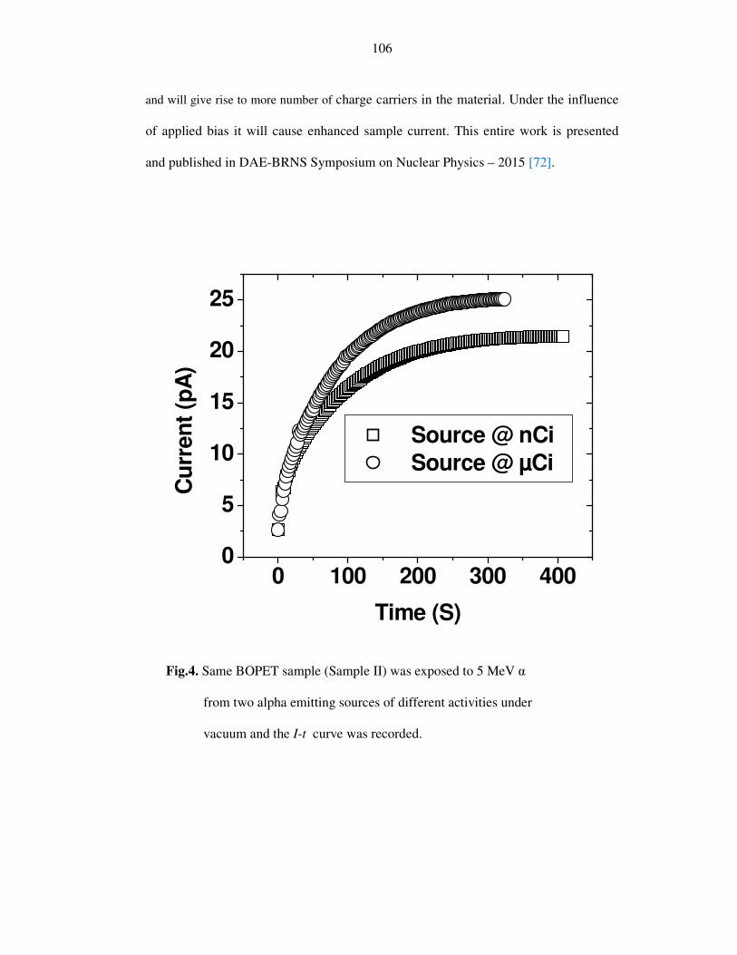
106
and will give rise to more number of charge carriers in the material. Under the influence
of applied bias it will cause enhanced sample current. This entire work is presented
and published in DAE-BRNS Symposium on Nuclear Physics – 2015 [72].
0 100 200 300 4000
5
10
15
20
25
Cu
rren
t (p
A)
Time (S)
Source @ nCi
Source @ µCi
Fig.4. Same BOPET sample (Sample II) was exposed to 5 MeV α
from two alpha emitting sources of different activities under
vacuum and the I-t curve was recorded.
107
5.4 CONCLUSION
If some radiation is incident on a polymer, then for polymer like BoPET, the
immediate change will be that it becomes opaque. It is well known that every polymer
is having its own ‘glass transition temperature’. If the temperature of a polymer is
raised above its glass transition temperature, then whatever changes happened in the
polymer during its exposure to radiation will be lost. So whatever opaqueness took
place in BoPET due to its exposure to radiation will disappear (i.e. will heal up), in
case its temperature is raised above its glass transition temperature.

108
_____________________________________
Chapter 6
CONCLUSION AND FUTURE SCOPE
_____________________________________

109
High quality nuclear radiation detectors will always remain as an important tool to
conduct various nuclear physics experiments and experiments are the only available
routes to unfold many mysteries pertaining to nuclear phenomenon and radiations.
The topic ‘Nuclear Radiation Detectors’ is vast and the scope of this thesis limits the
topics to only silicon and polymer based charged particles detectors. However, the
major areas of concern for silicon based detectors are (a) higher leakage current and
(b) stable long term behaviour. Various avenues have been explored and presented in
this thesis to address these two major issues but still there is scope to do some more
work. The summary of this thesis is given below:
An introductory discussion on radiation detection, origin of radioactivity, various
radiation sources, interaction of radiation with matter, various types of radiation
detectors, criterion to select right material for radiation detectors, definition of energy
resolution, factors affecting energy resolution, various components of leakage current
and nuclear electronics etc. has been given in the first chapter. This thesis work has
dealt mainly with use of organic materials for nuclear detectors. In nuclear detectors
organic materials can find different roles such as, active layer in organic/Si hybrid
structures (as detailed in Chapter 2), as a passivation layer in Si-based alpha detectors
(described in details in Chapter 3) and pure organic material as an active layer (as
presented in Chapter 5). This thesis also dealt with a novel surface cleaning
methodology using cold plasma flexible brush which has been adopted successfully to
clean silicon surface and subsequently used to fabricate silicon surface barrier
detectors. These detectors offered better performance than the conventionally prepared
(i.e. silicon surface cleaned by inorganic/organic chemicals) silicon surface barrier
detectors. This work has been described at length in Chapter 4.

110
Though lots of effort has been put and basic studies (as proof of concept) in each
aspect have been carried out, there is still further scope for improvement. All these
works can be considered as future scope of this thesis and are listed as given below:
(a) Study of aging of nuclear detectors based on n-silicon/copper-phthalocyanine
heterojunction was carried out where the electrical and alpha particle characteristics of
these detectors were studied after a long gap of 3 – 5 years and the best result obtained
from one detector (five year old) was reported. Similar studies can be conducted for
n-silicon/cobalt-phthalocyanine heterojunction detectors whose ‘As prepared’ and
‘Fifteen months after fabrication’ performances were already carried out. Further
study over a longer duration will confirm more affirmatively the very long term
performance of n-silicon/Metal-phthalocyanine heterojunction detectors.
(b) In passivation studies of silicon using tin oxide, 95-100 layers of ODA-Stannate
complex was initially deposited at the edges of silicon which after thermal
decomposition gave rise to a thick tin oxide layer. Fresh samples with 60 and 30
number of ODA-Stannate layers may be attempted to get thinner tin oxide layers.
Thinner the tin oxide layer, larger will be its resistance and perhaps lesser will be
leakage current through it. This aspect of optimizing the tin oxide layer thickness may
be explored. Secondly, passivation of silicon surface using hydrogenated amorphous
silicon layer can be explored exhaustively on some more silicon samples in order to
give this problem a logical end.
(c) With regard to plasma cleaning of silicon surface, some more plasma conditions
pertaining to mixed exposure may be explored by varying time of plasma exposure for
each of its two components viz. ‘Argon with laboratory Air’ and ‘Argon with moist
Air’ for further optimization of device performance.

111
(d) Lastly for all the fabricated detectors, apart from the off-line tests with radioactive
emitters, one can perform measurements using heavy ions from accelerator facilities
e.g. at FOTIA (BARC) or PELLETRON (TIFR). This will give better idea about
longevity of the detectors and how leakage current changes with fluence of heavy and
light ions.

112
_____________________________________
REFERENCES
_____________________________________

113
[1] G.F.Knoll, Radiation Detection and Measurements, 4th Edition, John Wiley and
Sons, New York, 2010, ISBN-10: 0470131489.
[2] William J. Price, Nuclear Radiation Detection, McGraw-Hill Book Company
[3] McKay K.G., Phys. Rev., 1951, 84, 829-832.
[4] M.Rizzi, M.D.Aloia and B.Castagnolo, J. Applied Sci., 2010, 10(23), 3141-3155.
[5] D.A.Bromley, IRE Trans. Nucl. Sci., 1962, NS-9(3), 135.
[6] E.E.Haller, H.W.Kraner and W.A.Higinbotham, Nuclear Radiation Detector
Materials (Materials Research Society Symposia Proceedings-Volume 16), Elsevier
Science Publishing Co., Inc., New York, 1983, ISBN 0-444-00787-3-Elsevier.
[7] Alan Owens, Compound Semiconductor Radiation Detectors, Taylor & Francis
Group, Boca Raton – USA, 2012, ISBN 978-1-4398-7312-0.
[8] Jan Jakubek, Andrea Cejnarova, Tomas Holy, Stanislav Pospisil, Josef Uher,
Zdenek Vykydal, Nucl. Instru. & Methods, 2008, 591, 155 -158.
[9] M.J.Yaffe and J.A.Rowlands, Phys. Med. Biol., 1997, 42, 1 – 39.
[10] W.D.Davis, J. of Appl. Phys., 1958, 29, 231 – 232.
[11] S.S.Friedland, J.W.Mayer, J.M.Denney and Frank Keywell, Review of Scientific
Instruments, 1960, 31, 74-75.
[12] E.M.Pell, J. Appl. Phys., 1960, 31, 291-302.
[13] J.H.Elliott, Nucl. Instru. & Methods, 1961, 12, 60-66.
[14] D.V.Freck and J.Wakefield, Nature, 1962, 193, 669.
[15] F.W.Martin, W.J.King and S.Harrison, IEEE Trans. on Nucl. Sci., 1964, NS-11,
280-285.
[16]W.Akutagawa, K.Zanio and J.Mayer, Nucl. Instru. & Methods, 1967, 55, 383-385.
[17] J.Llacer, Nucl. Instru. & Methods, 1972, 98, 259-268.

114
[18] J.E.Eberhardt, R.D.Ryan and A.J.Tavendale, Appl. Phys. Lett., 1970, 17, 427-429.
[19] W.R.Willig, Nucl. Instru. & Methods, 1971, 96, 615-616.
[20] S.F.Kozlov, IEEE Trans. on Nucl. Sci., 1975, NS-22, 160-170.
[21] E.Gatti and P.Rehak, Nucl. Instru. & Methods, 1984, 225, 608-661.
[22] N.Tsoulfanidis, Measurement and Detection of Radiation, 2nd
Edition,
Taylor and Francis, London, 1995, ISBN-10: 1560323175.
[23] Y.K.Akimov, Instrum. Exp. Techn., 2007, 50, 1-28.
[24] G.Lutz, Semiconductor Radiation Detectors: Device Physics, Springer,
Berlin, Heidelberg, 2007, ISBN-10: 3540716785.
[25] J.B.Mitchell, S.Agami and J.A.Davies, Radiation Effects and Defects in Solids,
1976, 28, 133-139.
[26] Sipra Choudhury, C.A. Betty and K.G.Girija, Thin Solid Films, 2008, 517,
923- 928.
[27] Sipra Choudhury, C.A.Betty and K.G.Girija BARC Newsletter, Jan-Feb 2011,
Issue No.318, 39 – 44 (Available online at http://www.barc.gov.in).
[28] Ming L. Tarng and Jacques I. Pankove, IEEE Transactions on Electron
Devices, 1979, ED-26, 1728-1734.
[29] William L.Hansen and Frederick S.Goulding, California Digital Library,
University of California, Lawrence Radiation Laboratory, 1964, 1-15.
[30] A.Ray, S.K.Gupta and J.V.Yakhmi, Radiation Measurements, 2009, 44, 47- 49.
[31] A.Ray and S.K.Gupta, AIP Conference Proceedings, 2013, 1512, 458-459.
doi: 10.1063/1.4791109.
[32] A.Ray, R.Prasad, C.A.Betty and T.V.Chandrasekhar Rao, Radiation Physics and
Chemistry, 2016, 120, 12-16.

115
[33] Khalil Arshak, Arousian Arshak, Saleh Zleetni and Ogla Korostynska, IEEE
Trans. on Nucl. Sci., 2004, 51(5), 2250-2255.
[34] Matjaz Kozelj, Bruno Cvikl, Dean Korošak, Proceedings of the International
Conference on Nuclear Energy for New Europe, Portorož, Slovenia,
September18–21, 2006, p.306.1–306.10
[35] A.G.Holmes-Siedle and L.Adams, Handbook of Radiation Effects,
Oxford Univ. Press, Oxford, U.K., 1993.
[36] S.R.Forrest, M.L.Kaplan and P.H.Shmidt, J. Appl. Phys., 1983, 55(6), 1492-1507.
[37] A.Al-Mohamad, C.W.Smith, I.Al-Saffar and M.Slifikin, Thin Solid Films,
1990, 189, 175-181.
[38] D.G.Zhu, D.F.Cui, M.Harris and M.C.Petty, Sensors and Actuators B, 1993, 12,
111- 114.
[39] P.S.Vukusic and J.R.Sambles, Thin Solid Films, 1992, 221, 311-317.
[40] J.Assaf and A.Al-Mohamad, Radiation Measurements, 2000, 32, 153-158.
[41] Y.Y.Zhang, S.X.Du and H.-J.Gao, Phys .Rev.B, 2011, 84, 125446-1 – 125446-8.
[42] D.C.Northrop and D.C.Puddy, Nucl. Instru. & Methods, 1971, 94, 557-559.
[43] J.Kemmer, Nucl. Instru. & Methods, 1984, 226, 89-93.
[44] P.Burger and Y.Beroud, Nucl. Instru. & Methods, 1984, 226, 45-49.
[45] F.S.Goulding and B.G.Harvey, Ann. Rev. Nucl. Sci., 1975, 25, 167-228.
[46] A.Ray, D.K.Aswal, R.Prasad and S.K.Gupta, Proc. of the DAE Symp. on Nucl.
Phys., 2013, 58, 848-849. [Available online at www.sympnp.org/proceedings].
[47] H.J.Langmann and O.Mayer, Nucl. Instru & Methods, 1966, 44, 55-60.
[48] E.D.Klema, IEEE Trans. on Nucl. Sci., 1965, NS-12, 288-290.
[49] W.L. Weiss, IEEE Trans. on Nucl. Sci.,1963, NS-10, 202-210.

116
[50] R.J.Fox, and C.J.Borkowski, IRE Trans. on Nucl. Sci., 1962, NS-9, 213-216.
[51] G.Anderson – Lindstrom and B.Zausig, Nucl. Instru. & Methods, 1966, 40,
277-290.
[52] G.Dearnaley and A.B.Whitehead, AERE-R 3662; Nucl. Instru. & Methods, 1961,
12, 205-226.
[53] M.Stojanovic, P.Osmokrovic, F.Boreli, D.Novkovic and R.Webb, Thin Solid
Films,1997, 296, 181-183.
[54] A.Ray, Shovit Bhattacharya, Ranu Bhatt, D.K.Aswal and S.K.Gupta,
31st IARP National Conference on Advances in Radiation Measurement Systems
and Techniques (IARPNC – 2014), 2014, P.-269.
[55] A.Ray, Shilpa Sawant, Sipra Choudhury and J.V.Yakhmi, Proceedings of the
DAE Solid State Physics Symposium, 2003, 46, 293-294.
[56] William C. O’Mara, Robert B. Herring and Lee P. Hunt, Handbook of
semiconductor silicon technology, Noyes Publications, New Jersey, 1990, ISBN
0-8155-1237-6.
[57] Werner Kern, J. Electrochem. Soc., 1990, 137, 1887 – 1892.
[58] Richard E. Novak, Jerzy Rużyłło, Takeshi Hattori, Cleaning Technology in
Semiconductor Device Manufacturing: Proceedings of the Sixth International
Symposium, The Electrochemical Society, Inc., 2000, 99 – 36, P.- 3.
[59] Sara B. Habib, Eleazar Gonzalez II and Robert F. Hicks, Journal of Vacuum
Science and Technology, 2010, A 28, 476-485.
[60] J. Jeong, J. Park, I. Henins, S. Babayan, V. Tu, G. Selwyn, G. Ding and
R.F.Hicks, J. Phys. Chem. A, 2000, 104, 8027-8032.

117
[61] E. Gonzalez II, M.D.Barankin, P.C. Guschl and R.F. Hicks, Langmuir, 2008, 24,
12636-12643.
[62] Dana Skacelova, Petr Sladek, Pavel Stahel, Lucas Pawera, Martin Hanicinec,
Jurgen Meichsner, Mirko Cernak, De Gruyter Open Chem., 2015, 13, 376–381.
[63] S. M. Sze and Kwok K.NG, Physics of Semiconductor Devices, John Wiley and
Sons, New Jersey, 2007.
[64]P.Siffert, and E.Krimmel, Silicon: Evolution and future of a technology, Springer-
Verlag, New York, 2004, P.-22.
[65] Savas Kaya, Parthiban Rajan, Harshita Dasari, David C. Ingram, Wojciech
Jadwisienczak, Faiz Rahman, ACS Applied Materials and Interfaces, 2015, 7,
25024-25031.
[66] A.K.Ray, Thin Solid Films, 1981, 84, 389 - 396.
[67]S.Taylor, J.F.Zhang, W.Eccleston, Semicond. Sci. Technol., 1993, 8, 1426 – 1433.
[68] Tomi Nath Das, Vadlamani Perayya, Prakash Gidomal Abichandani, Design of
cold plasma flexible brush and evaluation of its oxidizing plume, IEEE Trans. on
Plasma Sci., 2018, 46, 2536-2545.
[69] A.Ray, Tomi Nath Das, C.A.Betty , T.V.Chandrasekhar Rao, Journal of
Instrumentation, 2018, JINST 13 P09019.
[70] Dario Natali and Marco Sampietro, Nucl. Instru. & Methods A, 2003, 512 ,
419 - 426.
[71] Samuel Glasstone & Alexander Sesonske, Nuclear Reactor Engineering, Third
Indian Edition, CBS Publishers & Distributors, P. – 77.
[72] A.Ray, Proceedings of the DAE-BRNS Symp. on Nucl. Phys., 2015, 60,
956 – 957 [Available online at www.sympnp.org/proceedings].