Embed Size (px)
Citation preview

STUDY OF Mg2Si-BASED THERMOELECTRIC MATERIALS
A Thesis Submitted to the College of
Graduate Studies and Research
In Partial Fulfillment of the Requirements
For the Degree of Doctor of Philosophy
In the Department of Physics and Engineering Physics
University of Saskatchewan
Saskatoon
By
JIANBAO ZHAO
Copyright Jianbao Zhao, April, 2016. All rights reserved.
i
Permission to Use
In presenting this thesis in partial fulfilment of the requirements for a Postgraduate
degree from the University of Saskatchewan, I agree that the Libraries of this University may
make it freely available for inspection. I further agree that permission for copying of this thesis
in any manner, in whole or in part, for scholarly purposes may be granted by the professor or
professors who supervised my thesis work or, in their absence, by the Head of the Department or
the Dean of the College in which my thesis work was done. It is understood that any copying or
publication or use of this thesis or parts thereof for financial gain shall not be allowed without
my written permission. It is also understood that due recognition shall be given to me and to the
University of Saskatchewan in any scholarly use which may be made of any material in my
thesis.
Requests for permission to copy or to make other use of material in this thesis in whole or
part should be addressed to:
Head of the Department of Physics and Engineering Physics
116 Science Place
University of Saskatchewan
Saskatoon, Saskatchewan
Canada
S7N 5E2
ii
ABSTRACT
Mg2Si-based thermoelectrics are currently the most promising, environmentally benign
and inexpensive materials for power generation. The objective of this thesis is to characterize
Mg2Si-based thermoelectric materials using state-of-the-art synchrotron radiation techniques
including infrared reflectivity/absorption spectroscopy and high resolution X-ray powder
diffraction. This is complemented by density functional theory (DFT) calculations. Also reported
here is the main research: the analysis of the electronic structure and transport properties of
doped Mg2Si using experimental and theoretical methods.
To enhance the thermoelectric performance, Mg2Si doped with a single component of Bi
or Sb were studied. The investigation showed by doping the electron carrier concentrations were
increased. In particular, dc conductivities of the doped samples were extracted from the analysis
of infrared reflectivity spectra employing the Drude free electron model. We found the
conductivity was lower when determined by infrared measurements rather than in-situ four point
probe measurements of the bulk sample because of the limited penetration depth of infrared (IR)
radiation and the very small spot size. In particular, we were able to extract the electrical
conductivity, relaxation times and electron effective masses of the samples. DFT calculations
reproduced the experimental observations and show a substantial increase in the Seebeck
coefficients.
The next step was to study the effect after doping with two different dopants. For this
purpose, we investigated the effect of Ge substitute Si in Bi doped Mg2Si. In particular, the dc
conductivities of the doped samples were extracted from the analysis of infrared reflectivity
spectra. From the IR data, we extracted the relevant parameters for electrical transport. The
experimental data were explained with theoretical DFT calculations in which the calculated
densities of states (DOS) of the Ge- and Bi-doped Mg2Si samples were found to be very similar,

iii
and therefore to have comparable Seebeck coefficients. The steep curvatures of the DOS at the
Fermi level indicate a light electron band. We found the thermal conductivity of Mg2Si is
substantially lower from 7 Wm-1K-1 to 2.7 Wm-1K-1 in Mg2Si0.677Ge0.3Bi0.023 at 300 K. A
performance figure of merit of 0.7 was achieved at 773 K for this sample.
We further investigated the effect of multi-doping with Sb, Al and Zn on the
enhancement of the thermoelectric and electrical transport properties of Mg2Si. A maximum ZT
of 0.964 was found for Sb0.5%Zn0.5% doped Mg2Si (Mg1.995Zn0.005Si0.995Sb0.005) at 880 K. This
value is comparable to those of PbTe based thermoelectrics which are the currently the materials
used in commercial products.
We also studied the effect of pressure on the thermoelectric performance of a Al-doped
Mg2Si sample. From in-situ X-ray diffraction, we observed a structural transform in which the
electrical conductivity was increased after the phase transition. The experimental observed
maximum thermoelectric power at 1.9 GPa was reproduced by DFT calculations and explained
by the increase of electronic density of states at the Fermi level.
The effect of multi-wall carbon nanotubes (MWCNTs) to increase the electrical
conductivity of Mg2Si0.877Ge0.1Bi0.023 was examined. At 323 K the conductivity was found to
increase from 450 Ω-1cm-1 to 500 Ω-1cm-1. However, this effect diminished at higher temperature
and the conductivity drop to 470 Ω-1cm-1 at 773 K. Raman study showed the persistent of
disorder (D) and tangential (G) mode characteristics of a carbon nanotube in the doped sample
indicating that there was no decomposition or substantial chemical reaction of the MWCNTs
with Mg2Si0.877Ge0.1Bi0.023.
Finally, we present the results on the analysis of valence electron topologies of Mg2Si
multi-doped with Al, Zn and Sb thermoelectric materials by the Maximum Entropy Method

iv
(MEM) using data obtained from synchrotron X-ray powder diffraction measurements. The
results showed the qualitative feature of valence electron distributions were correctly located.
However, due to the limited number of Bragg diffraction peaks in the experimental patterns, the
effect of the dopants to the core charge density cannot be reliably obtained. An error analysis
was performed from the analysis of diffraction pattern of Al-doped Mg2Si which included high
angle Bragg reflections. We concluded that the density maps extracted from MEM analysis of
the doped samples were qualitatively correct.

v
ACKNOWLEDGMENTS
First, I would like to warmly and sincerely thank my supervisor Dr. John S. Tse for the
guidance, understanding, patience, and mostly important his continuous and instructive
supervision. The thesis has benefited greatly from his guidance. He encouraged me not only to
be a physicist but also as an independent researcher with strong motivation and commitment. In
particular, I wish to thank him for finding time to help even with an extremely busy schedule.
I would especially like to thank all the faculty members in the Department of Physics and
Engineering Physics at University of Saskatchewan. Especially, I am truly grateful to Dr. Tse’s
group members Xue Yong, Niloofar Zarifi, Jianjun Yang, Hanyu Liu, and Min Wu for their
constant supports and help during my research.
Most results in this thesis have been published as academic papers. I would like to thank
all the co-authors for their contributions to the manuscripts. In particular to Dr. Holger Kleinke
(University of Waterloo) who provided most of samples studied here and Dr. Zhenxian Liu,
beamline scientist at U2A, Brookhaven National Laboratory for his instruction to perform far
and mid infrared transmission and reflectivity measurements.
I am gratefully indebted to my wife Yang Yang, my parents and my parents-in-law for
their everlasting and unconditional love, support, and encouragement during my Ph.D study. In
particular, to my baby daughter Emma Zhao, she made me to be a super multitasker.
Last, but certainly not least, I am very grateful to Argonne National Laboratory, Canadian
Light Source, Brookhaven National Laboratory, West Grid Canada and AUTO21 for the use of
their facilities and the funding supports on my projects.
vi
TABLE OF CONTENTS
Permission to Use i
ABSTRACT ii
ACKNOWLEDGMENTS v
TABLE OF CONTENTS vi
LIST OF TABLES x
LIST OF FIGURES xi
LIST OF ABBREVIATIONS xvii
CHAPTER 1 INTRODUCTION 1
1.1 Thermoelectric effects and Performance index ..................................................................... 1
1.2 Figure of merit (ZT)............................................................................................................... 2
1.3 Mg2Si-based thermoelectric materials .................................................................................. 4
1.4 Strategies to enhance the efficiency of Mg2Si-based thermoelectric materials .................... 7
1.5 Thesis organization ............................................................................................................... 9
1.6 Research contributions ........................................................................................................ 10
References ................................................................................................................................. 11
CHAPTER 2 EXPERIMENTAL AND THEORETICAL METHODS 15
2.1 Experimental methods ......................................................................................................... 15
2.1.1 Infrared reflectivity spectra measurement 15
2.1.2 Infrared absorption spectra measurement 21
2.1.3 Synchrotron Powder X-ray diffraction measurements 22
2.1.4 Maximum Entropy Method (MEM) 23
2.2 Theoretical methods ............................................................................................................ 27
2.2.1 Density functional theory (DFT) 28
2.2.2 Electronic structure calculation-Electronic density of states (DOS) and Projected
electronic density of states (PDOS) 30
2.2.3 GW approximation (GWA) 30
2.2.4 Temperature dependent Seebeck coefficient S(T) calculation 31
References ................................................................................................................................. 32

vii
CHAPTER 3 SB- AND BI- DOPED MG2SI:LOCATION OF THE DOPANTS, MICRO- AND
NANOSTRUCTURES, ELECTRONIC STRUCTURES AND THERMOELECTRIC
PROPERTIES 34
Abstract ..................................................................................................................................... 36
3.1 Introduction ......................................................................................................................... 37
3.2 Experiment .......................................................................................................................... 38
3.2.1 Syntheses and phase purity analyses 38
3.2.2 Transmission electron microscopy 40
3.2.3 Electronic structure calculations 41
3.2.4 Physical property measurements 42
3.3 Results and discussion ......................................................................................................... 44
3.3.1 Micro- and nanostructure 44
3.3.2 Electronic structure 46
3.3.3 Physical properties 49
3.4 Conclusions ......................................................................................................................... 56
Acknowledgements ................................................................................................................... 56
References ................................................................................................................................. 57
CHAPTER 4 LOCAL STRUCTURE AND THERMOELECTRIC PROPERTIES OF
MG2SI0.977-XGEXBI0.023 (0.1≤ X ≤ 0.4) 60
Abstract ..................................................................................................................................... 62
4.1 Introduction ......................................................................................................................... 62
4.2 Experiment .......................................................................................................................... 64
4.3 Results and discussion ......................................................................................................... 68
4.4 Conclusions ......................................................................................................................... 81
Acknowledgements ................................................................................................................... 82
References ................................................................................................................................. 82
CHAPTER 5 THERMOELECTRIC AND ELECTRICAL TRANSPORT PROPERTIES OF
MG2SI MULTI-DOPED WITH SB, AL AND ZN 86
Abstract ..................................................................................................................................... 88
5.1 Introduction ......................................................................................................................... 89
5.2 Experimental details ............................................................................................................ 92
viii
5.2.1 Synthesis and the sintering process for doped Mg2Si sample preparation 92
5.2.2 Powder X-ray diffraction measurements 93
5.2.3 Mid-infrared reflectivity measurements 93
5.2.4 Electrical transport property and thermoelectric property measurements 94
5.3 Results and discussion ......................................................................................................... 95
5.4 Conclusions ....................................................................................................................... 111
Acknowledgements ................................................................................................................. 111
References ............................................................................................................................... 112
CHAPTER 6 PRESSURE-INDUCED PHASE TRANSITION AND ELECTRICAL
PROPERTIES OF THERMOELECTRIC AL-DOPED MG2SI 115
Abstract ................................................................................................................................... 117
6.1 Introduction ....................................................................................................................... 117
6.2 Experiment ........................................................................................................................ 120
6.3 Results and Discussion ...................................................................................................... 122
6.4 Conclusion ......................................................................................................................... 143
Acknowledgements ................................................................................................................. 144
References ............................................................................................................................... 145
CHAPTER 7 ENHANCED FIGURE OF MERIT IN MG2SI0.877GE0.1BI0.023/MULTI WALL
CARBON NANOTUBE NANOCOMPOSITIES 148
Abstract ................................................................................................................................... 150
7.1 Introduction ....................................................................................................................... 151
7.2 Experimental section ......................................................................................................... 153
7.2.1 Transmission electron microscopy 155
7.2.2 Raman spectroscopy 156
7.3 Results and discussion ....................................................................................................... 156
7.4 Conclusions ....................................................................................................................... 170
Acknowledgements ................................................................................................................. 170
References ............................................................................................................................... 171
CHAPTER 8 CHARGE DENSITIES OF MULTI-DOPED MG2SI THERMOELECTRIC
MATERIALS USING THE MAXIMUM ENTROPY METHOD 174
Abstract ................................................................................................................................... 176

ix
8.1 Introduction ....................................................................................................................... 176
8.2 Experimental details .......................................................................................................... 179
8.2.1 Synthesis and Sintering Process for Preparation of Doped Mg2Si Samples .................. 179
8.2.2 X-ray Powder Diffraction Measurements ...................................................................... 180
8.2.3 Maximum Entropy Method (MEM) ............................................................................... 180
8.2.4 Electronic Structure Calculations ................................................................................... 181
8.3 Results and Discussion ...................................................................................................... 181
8.4 Conclusion ......................................................................................................................... 197
Acknowledgments ................................................................................................................... 197
References ............................................................................................................................... 198
CHAPTER 9 SUMMARY AND PERSPECTIVES 201
9.1 Summary ........................................................................................................................... 201
9.2 Perspectives ....................................................................................................................... 205
References ............................................................................................................................... 206
APPENDIX A 207
APPENDIX B 209
APPENDIX C 211
x
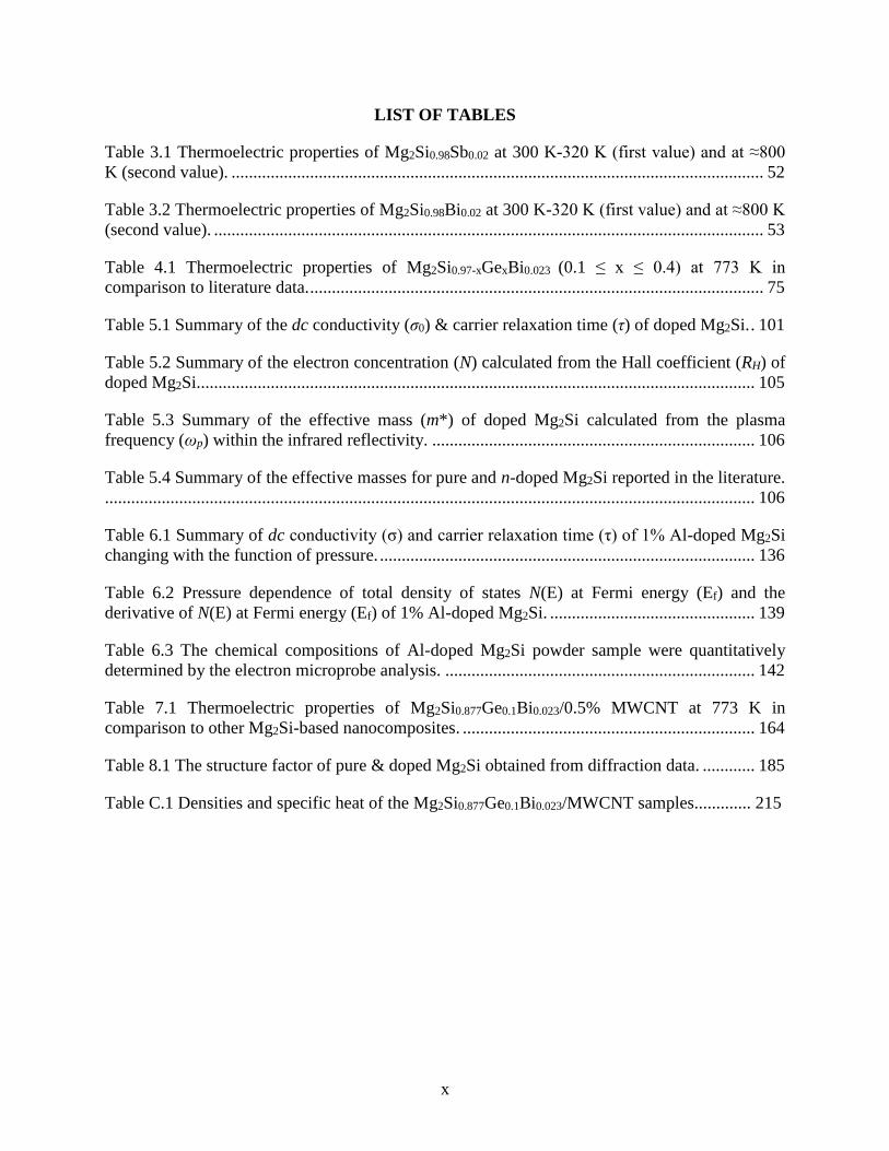
LIST OF TABLES
Table 3.1 Thermoelectric properties of Mg2Si0.98Sb0.02 at 300 K-320 K (first value) and at ≈800
K (second value). .......................................................................................................................... 52
Table 3.2 Thermoelectric properties of Mg2Si0.98Bi0.02 at 300 K-320 K (first value) and at ≈800 K
(second value). .............................................................................................................................. 53
Table 4.1 Thermoelectric properties of Mg2Si0.97-xGexBi0.023 (0.1 ≤ x ≤ 0.4) at 773 K in
comparison to literature data. ........................................................................................................ 75
Table 5.1 Summary of the dc conductivity (σ0) & carrier relaxation time (τ) of doped Mg2Si. . 101
Table 5.2 Summary of the electron concentration (N) calculated from the Hall coefficient (RH) of
doped Mg2Si................................................................................................................................ 105
Table 5.3 Summary of the effective mass (m*) of doped Mg2Si calculated from the plasma
frequency (ωp) within the infrared reflectivity. .......................................................................... 106
Table 5.4 Summary of the effective masses for pure and n-doped Mg2Si reported in the literature.
..................................................................................................................................................... 106
Table 6.1 Summary of dc conductivity (σ) and carrier relaxation time (τ) of 1% Al-doped Mg2Si
changing with the function of pressure. ...................................................................................... 136
Table 6.2 Pressure dependence of total density of states N(E) at Fermi energy (Ef) and the
derivative of N(E) at Fermi energy (Ef) of 1% Al-doped Mg2Si. ............................................... 139
Table 6.3 The chemical compositions of Al-doped Mg2Si powder sample were quantitatively
determined by the electron microprobe analysis. ....................................................................... 142
Table 7.1 Thermoelectric properties of Mg2Si0.877Ge0.1Bi0.023/0.5% MWCNT at 773 K in
comparison to other Mg2Si-based nanocomposites. ................................................................... 164
Table 8.1 The structure factor of pure & doped Mg2Si obtained from diffraction data. ............ 185
Table C.1 Densities and specific heat of the Mg2Si0.877Ge0.1Bi0.023/MWCNT samples............. 215

xi
LIST OF FIGURES
Fig. 1.1 Power generation (a) and refrigeration (b) of thermoelectric modules. [1] ....................... 2
Fig. 2.1 Infrared reflectivity spectra measurement of HBBO under different pressures. (The band
marble “Diamond” was undesirable contribution of the C-C stretch from the diamond anvils.) . 19
Fig. 2.2 (left) dc conductivity calculated of HBBO from the reflectance as a function of pressure.
....................................................................................................................................................... 20
Fig. 2.3 (right) ac conductivity measured of HBBO by four probe method as a function of
pressure. ........................................................................................................................................ 20
Fig. 2.4 Infrared absorption spectra of pure Mg2Si. ..................................................................... 22
Fig. 2.5 Bragg’s Law. ................................................................................................................... 23
Fig. 2.6 3D iso-surface of the electron density of Mg2Si in the unit cell superimposed on the
structure of Mg2Si. (Si atom is at the origin). The eight Mg atoms are seen inside the cubic unit
cell at ±(1/4 1/4 1/4). [8] ............................................................................................................... 27
Fig. 3.1 (a) and (b) STEM-HAADF image of Mg2Si0.98Bi0.02. (c) and (d) Multi-slice simulation
results obtained for Mg2Si0.98Bi0.02 and Mg2Si along the [110] zone axis, respectively. .............. 45
Fig. 3.2 (a) Atomic-resolution STEM-HAADF image of Mg2Si0.98Bi0.02 demonstrating Bi
segregation at the grain boundary (GB). (b) STEM-HAADF image acquired from the region
marked in yellow in (a). (c) EDX line-scan for Bi (red) over the same area marked in yellow. .. 46
Fig. 3.3 Density of states (left) and absorbance spectrum (right) of Mg2Si. ................................ 47
Fig. 3.4 Density of states of Mg64Si31Sb (left) and Mg64Si31Bi (right). ........................................ 48
Fig. 3.5 Calculated Seebeck coefficients of Mg2Si1-xSbx. ............................................................ 49
Fig. 3.6 Reflectivity spectra (left and center) and optical conductivity (right) of Mg2Si0.98Sb0.02
and Mg2Si0.98Bi0.02. ....................................................................................................................... 50
Fig. 3.7 Carrier concentration (left) and Hall mobility and electrical conductivity (right) of
Mg2Si0.98Sb0.02 (white symbols) and Mg2Si0.98Bi0.02 (black symbols). ......................................... 51
Fig. 3.8 Electrical conductivity (left) and Seebeck coefficient (right) of Mg2Si0.98Sb0.02 (white
symbols) and Mg2Si0.98Bi0.02 (black symbols). ............................................................................. 54
Fig. 3.9 Thermal conductivity (left) and estimated figure of merit (right) of Mg2Si0.98Bi0.02. ..... 55

xii
Fig. 4.1 Density of states of Mg2Si0.969-xGexBi0.031 (0.094 ≤ x ≤ 0.375). ...................................... 68
Fig. 4.2 Low-magnification STEM-HAADF image of Mg2Si0.777Ge0.2Bi0.023. (b) and (c) STEM-
HAADF image obtained from the red and green marked areas in (a) displaying the higher
concentration of heavy atoms. (d) STEM-HAADF image corresponding to the region marked in
(b) together with atomic simulation results showing the occupation of interstitial sites marked by
red lines as well as the heavy atom segregation on Si sites marked by blue lines. (For
interpretation of the references to color in this figure legend, the reader is referred to the web
version of this article.) .................................................................................................................. 70
Fig. 4.3 Thermal conductivity of Mg2Si0.977-xGexBi0.023 (0.1 ≤ x ≤ 0.4). ...................................... 71
Fig. 4.4 Lattice thermal conductivity of Mg2Si0.977-xGexBi0.023 (0.1 ≤ x ≤ 0.4). ........................... 73
Fig. 4.5 Electrical conductivity of Mg2Si0.977-xGexBi0.023 (0.1 ≤ x ≤ 0.4). .................................... 74
Fig. 4.6 Reflectivity spectra of Mg2Si0.977-xGexBi0.023 (x = 0.2, 0.4)............................................. 76
Fig. 4.7 Carrier concentration of Mg2Si0.977-xGexBi0.023 (x = 0.3, 0.4). ......................................... 78
Fig. 4.8 Hall mobility of Mg2Si0.977-xGexBi0.023 (x = 0.3, 0.4). ..................................................... 78
Fig. 4.9 Seebeck coefficient of Mg2Si0.977-xGexBi0.023 (0.1 ≤ x ≤ 0.4). ......................................... 80
Fig. 4.10 Figure of merit of Mg2Si0.977-xGexBi0.023 (0.1 ≤ x ≤ 0.4). .............................................. 81
Fig. 5.1 Angle dispersive X-ray diffraction patterns of pure Mg2Si and doped Mg2Si measured at
room temperature. ......................................................................................................................... 96
Fig. 5.2 (a) Lattice parameters of pure and doped Mg2Si; (b) the volume per formula of pure and
doped Mg2Si.................................................................................................................................. 97
Fig. 5.3 Mid-infrared reflectivity spectra of pure and doped Mg2Si. ........................................... 98
Fig. 5.4 Temperature dependent electrical resistivity of doped Mg2Si by the conventional quasi-
four-probe method. ..................................................................................................................... 100
Fig. 5.5 A comparison of measured and fitted infrared reflectivity spectra of 0.5% Sb & 0.5% Zn
doped Mg2Si................................................................................................................................ 100
Fig. 5.6 A comparison of electrical resistivity (ρ) extracted from infrared reflectivity spectra and
measured by the quasi-four-probe method. ................................................................................ 103

xiii
Fig. 5.7 Hall coefficients (RH) of doped Mg2Si samples were measured by the quasi-four-probe
method......................................................................................................................................... 105
Fig. 5.8 Temperature dependent (a1) & (a2) electrical conductivity, (b) Seebeck coefficient, (c)
power factor, (d1) & (d2) thermal conductivity & lattice thermal conductivity, and (e) figure of
merit (ZT). ................................................................................................................................... 108
Fig. 6.1 Angle dispersive X-ray diffraction patterns of pure Mg2Si at selected pressures measured
at room temperature. ................................................................................................................... 124
Fig. 6.2 (a) Lattice parameters of pure Mg2Si as a function of pressure obtained in the present
study and compared with previous works. (b) The volume per formula of pure Mg2Si as a
function of pressure and compared with previous works. The red color lines are fits to 3rd order
Birch-Murnaghan equation of state. ........................................................................................... 124
Fig. 6.3 GW band structures of pure Mg2Si at 0.1, 4, 8, and 11 GPa. ........................................ 126
Fig. 6.4 Room temperature angle dispersive X-ray diffraction patterns of 1% Al-doped Mg2Si at
selected pressures. ....................................................................................................................... 127
Fig. 6.5 (a) Lattice parameters of anti-fluorite (Fm-3m), and anti-cotunnite (Pnma) phases for Al-
doped Mg2Si and pure Mg2Si as a function of pressure. (b) The volume per formula of Al-doped
Mg2Si and pure Mg2Si as a function of pressure. ....................................................................... 129
Fig. 6.6 Infrared reflectivity spectra of 1% Al doped Mg2Si under different pressures. ............ 131
Fig. 6.7 Comparison of the infrared reflectivity spectra of 1% Al-doped Mg2Si and pure Mg2Si
under ambient conditions. ........................................................................................................... 132
Fig. 6.8 A comparison of measured and fitted infrared reflectivity spectra of 1% Al doped Mg2Si
at 10.5 GPa. ................................................................................................................................. 133
Fig. 6.9 The change of the dc conductivities of 1% Al-doped Mg2Si changes with pressure. ... 134
Fig. 6.10 Total density of states and projected density of states for Al-doped Mg2Si at (a) 0.1
GPa, (b) 0.9 GPa, (c) 1.9 GPa, (d) 3.3 GPa, (e) 4.9 GPa, (f) 6.4 GPa, (g) 8.4 GPa, and (h) 10.3
GPa. ............................................................................................................................................. 135
Fig. 6.11 (a) The derivative of total density of states (dN(E)/dE)│Ef. (b) The magnitude of total
density of states at the Fermi level N(Ef) for Al-doped Mg2Si as a function of pressure. .......... 138
Fig. 6.12 Scanning electron microscopy (SEM) image of Al-doped Mg2Si powder sample. .... 141
xiv
Fig. 7.1 (a) Left: low-magnification STEM-HAADF image; right: EDX elemental maps of Mg,
Si, Ge and Bi in the area marked with a rectangle; (b), (c) line profiles of Ge-K and Bi-L lines
along the boundary between different grains. The profiles in red and green correspond to Ge and
Bi, respectively. .......................................................................................................................... 158
Fig. 7.2 (a) Low-magnification STEM-HAADF image; (b) and (c) Kikuchi patterns confirming
two different grains separated by a grain boundary; (d) EDX line scans of Ge-K (red) and Bi-L
(green) lines along the grain boundary; (e) line profiles of Ge (red) and Bi (green) along the grain
boundary as shown in (d). ........................................................................................................... 159
Fig. 7.3 (a and b) Atomic resolution STEM-HAADF images corresponding to a region in the
bulk of a grain oriented along [111] zone axis; (c) magnified region from (b), the green arrow
indicating an atomic column with no significant brighter intensities as compared to the atomic
column highlighted by the pink arrow. ....................................................................................... 160
Fig. 7.4 Raman spectra of the Mg2Si0.877Ge0.1Bi0.023/MWCNT samples. ................................... 161
Fig. 7.5 Electrical conductivity of the Mg2Si0.877Ge0.1Bi0.023/MWCNT samples. ...................... 162
Fig. 7.6 Room temperature carrier concentration of the Mg2Si0.877Ge0.1Bi0.023/MWCNT samples.
..................................................................................................................................................... 163
Fig. 7.7 Low temperature Hall mobility of the Mg2Si0.877Ge0.1Bi0.023/MWCNT samples. ......... 163
Fig. 7.8 Seebeck coefficient of the Mg2Si0.877Ge0.1Bi0.023/MWCNT samples. ........................... 165
Fig. 7.9 Power factor of MWCNT/Mg2Si0.877Ge0.1Bi0.023 samples. ............................................ 165
Fig. 7.10 Thermal conductivity of the Mg2Si0.877Ge0.1Bi0.023/MWCNT samples. ...................... 167
Fig. 7.11 Lattice thermal conductivity of the Mg2Si0.877Ge0.1Bi0.023/MWCNT samples. ........... 168
Fig. 7.12 Figure of merit of the Mg2Si0.877Ge0.1Bi0.023/MWCNT samples. ................................ 169
Fig. 8.1 (a) Angle dispersive X-ray diffraction patterns of pure Mg2Si and doped Mg2Si
measured at ambient conditions; (b) The expanded diffraction patterns between 9º to 12º of the
(111) peak. .................................................................................................................................. 183
Fig. 8.2 Le Bail fit to the experimental X-ray diffraction patterns for (a) pure Mg2Si; (b)
Mg1.99Al0.005Zn0.005Si0.995Sb0.005; (c) Mg1.995Zn0.005Si0.995Sb0.005; and (d) Mg1.99Zn0.01Si0.995Sb0.005.
..................................................................................................................................................... 184
Fig. 8.3 3D charge density of pure Mg2Si in the unit cell (The value of the contour surface is 0.5
e/Å3.) ........................................................................................................................................... 188
xv
Fig. 8.4 3D electron density difference (Δρ) of doped Mg2Si samples
(Mg1.99Al0.005Zn0.005Si0.995Sb0.005 (Sb0.5%Al0.5%Zn0.5%), Mg1.995Zn0.005Si0.995Sb0.005
(Sb0.5%Zn0.5%), and Mg1.99Zn0.01Si0.995Sb0.005 (Sb0.5%Zn1.0%)) relative to pure Mg2Si with
isosurface contour values of (a) 0.5 e/Å3 and (b) -0.5 e/Å3. ....................................................... 191
Fig. 8.5 2D electron density difference (Δρ) of doped Mg2Si samples
(Mg1.99Al0.005Zn0.005Si0.995Sb0.005 (Sb0.5%Al0.5%Zn0.5%), Mg1.995Zn0.005Si0.995Sb0.005
(Sb0.5%Zn0.5%), and Mg1.99Zn0.01Si0.995Sb0.005 (Sb0.5%Zn1.0%)) relative to pure Mg2Si in (a)
(100) and (b) (110) planes. The contour levels are shown in the side bars. ............................... 192
Fig. 8.6 Projected density of states (pdos) of Mg214Zn2Si104Al2Sb2 model (a) into atomic
composition; (b) into atomic orbitals. ......................................................................................... 194
Fig. 8.7 Projected density of states (pdos) of Mg212Zn2Al2Si106Sb2 model (a) into atomic
composition; (b) into atomic orbitals. ......................................................................................... 194
Fig. 8.8 Refined X-ray diffraction pattern for 1% Al-doped Mg2Si (Mg1.99Al0.01Si). ................ 196
Fig. 8.9 3D electron density difference of 1% Al-doped Mg2Si (Mg1.99Al0.01Si) (a) between 15
and 55 reflection peaks used; (b) between 20 and 55 reflection peaks used; (c) between 30 and 55
reflection peaks used; and (d) between 45 and 55 reflection peaks used. (Yellow: positive charge
density; Green: negative charge density) .................................................................................... 196
Fig. A.1 Experimental powder diagrams of Mg2Si and Mg2Si0.98Bi0.02......................................207
Fig. A.2 DSC and TG of Mg2Si0.98Bi0.02. .................................................................................... 207
Fig. A.3 Band structure of Mg2Si. Black: GGA, red: GW method. ............................................ 208
Fig. B.1 Experimental powder diagrams of Mg2Si0.977–xGexBi0.023 (0.1 ≤ x ≤ 0.4)..................... 209
Fig. B.2 Specific heat of Mg2Si0.977–xGexBi0.023 (x = 0.1, 0.4). ................................................... 209
Fig. B.3 Calculated Lorenz number of Mg2Si0.977–xGexBi0.023 (0.1 ≤ x ≤ 0.4). ........................... 210
Fig. C.1 Powder XRD patterns of Mg2Si0.877Ge0.1Bi0.023 samples.............................................. 211
Fig. C.2 SEM images of the Mg2Si0.877Ge0.1Bi0.023/1 wt.-% MWCNT sample. ......................... 212
Fig. C.3 Low-magnification structural and compositional analyses of the edge of a grain.
EDXelemental mapping over a selected area showing the distribution of Mg, Si, Ge and Bi. .. 213
Fig. C.4 Medium temperature thermal conductivity of all samples with respect to MWCNT
content. ........................................................................................................................................ 213
Fig. C.5 Lorenz number of all samples with regard to temperature. .......................................... 214

xvi
Fig. C.6 Power factor of two bars obtained from 0.5% MWCNT/Mg2Si0.877Ge0.1Bi0.023
nanocomposite (6% error is considered). .................................................................................... 214
xvii
LIST OF ABBREVIATIONS
2D Two-dimensional
3D Three-dimensional
CNT Carbon nanotube
DFT Density functional theory
DOS Density of states
DSC Differential scanning calorimetry
EOS Equation of states
EPMA Electron-probe microanalysis
EDX Energy dispersive X-ray
FCC Face-centered cubic
GGA Generalized gradient approximation
GB Grain boundary
GDMS Glow discharge mass spectrometry
H-K Hohenberg-Kohn
HBBO Prototypal oxobenzene-bridged 1,2,3-bisdithiazolyl radical conductor
HAADF High-angle annular dark-field
HRTEM High resolution transmission electron microscopy
IR Infrared
K-K Kramers–Kronig
LO Longitudinal-optical
MWCNT Multi-wall carbon nanotube
MEM Maximum Entropy Method
Mg2Si Magnesium silicide
PAW Projected augmented wave

xviii
PBE Perdew-Burke-Ernzerhof
PDOS Projected density of states
PbTe Lead telluride
SWCNT Single-wall carbon nanotube
STEM Scanning transmission electron microscopy
SCD Differential scanning calorimetry
TE Thermoelectric
TO Transverse-optical
TG Thermogravimetry
VASP Vienna Ab-initio Simulation Package
XC Exchange-correlation
XEDS X-ray Spectrometry
XRD X-ray diffraction
ZT Figure of merit
1
CHAPTER 1
INTRODUCTION
With the rapid development of the world’s economy in the past few decades, the supply
of cheap and clean energy has become the greatest bottleneck to industries and consumers.
Meanwhile, the environmental impact of the existing technology of power generation has
become severe. For example, with the increased number of vehicles and energy consumption in
emerging economies, the associated exhaust emissions have led to a global concern. It is widely
recognized that the removal of the emissions or, even more desirable, the conversion of the waste
heat into useable energy remains a major challenge and a promising area of research. The
purpose of this research is to identify improved thermoelectric materials based on Mg2Si, which
can efficiently convert heat into electricity and vice versa.
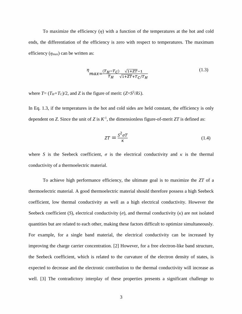
1.1 Thermoelectric effects and Performance index
Thermoelectric materials are based on two fundamental effects: the Seebeck effect and
Peltier effect. The Seebeck effect was first discovered by Thomas Johann Seebeck in the 1800s.
The modern day application of this effect is to generate an electrical current by applying a
temperature difference between the junctions of p- and n-doped semiconductors, in which
electronic charges from the hot end are diffused to the cold site as illustrated in Fig. 1.1(a). The
voltage generated (ΔV) is proportional to the temperature difference (ΔT) and the proportionality
constant (S =-ΔV/ΔT) is defined as the Seebeck coefficient. The Peltier effect is the reverse of the
Seebeck effect (Fig. 1.1(b)) and is defined as a temperature difference created by applying a
voltage between two connected n- and p-type semiconductors. When a current (I) is passed
between them, heat (Q) is generated or absorbed. The Peltier coefficient (π) is defined as π = Q/I.

2
Fig. 1.1 Power generation (a) and refrigeration (b) of thermoelectric modules. [1]
1.2 Figure of merit (ZT)
A thermoelectric converter is a heat engine and its operating principle obeys the laws of
thermodynamics. The efficiency (η) of a thermoelectric material is defined as follows,
𝜂 = 𝑒𝑛𝑒𝑟𝑔𝑦 𝑠𝑢𝑝𝑝𝑙𝑖𝑒𝑑 𝑡𝑜 𝑡ℎ𝑒 𝑙𝑜𝑎𝑑ℎ𝑒𝑎𝑡 𝑎𝑏𝑜𝑟𝑏𝑒𝑑 𝑎𝑡 ℎ𝑜𝑡 𝑗𝑢𝑛𝑐𝑡𝑖𝑜𝑛
(1.1)
If we assume that the electrical conductivity, thermal conductivity and Seebeck coefficient are
the same at both the hot and cold sides, the efficiency (η) can be expressed as:
𝜂 = 𝐼2𝑅
𝜆(𝑇𝐻−𝑇𝐶)−12
𝐼2𝑅 (1.2)
where λ is the thermal conductance of hot and cold sides, R is the electrical series resistance of
hot and cold ends (p-type and n-type legs are connected in series), and TH and TC are the
temperature in the hot side and cold side, respectively. [1]
(b) (a)
3
To maximize the efficiency (η) with a function of the temperatures at the hot and cold
ends, the differentiation of the efficiency is zero with respect to temperatures. The maximum
efficiency (ηmax) can be written as:
𝜂𝑚𝑎𝑥=
(𝑇𝐻−𝑇𝐶)
𝑇𝐻
√1+𝑍𝑇−1
√1+𝑍𝑇+𝑇𝐶/𝑇𝐻
(1.3)
where T= (TH+TC)/2, and Z is the figure of merit: (Z=S2/Rλ).
In Eq. 1.3, if the temperatures in the hot and cold sides are held constant, the efficiency is only
dependent on Z. Since the unit of Z is K-1, the dimensionless figure-of-merit ZT is defined as:
𝑍𝑇 = 𝑆2
𝜎𝑇𝜅
(1.4)
where S is the Seebeck coefficient, σ is the electrical conductivity and κ is the thermal
conductivity of a thermoelectric material.
To achieve high performance efficiency, the ultimate goal is to maximize the ZT of a
thermoelectric material. A good thermoelectric material should therefore possess a high Seebeck
coefficient, low thermal conductivity as well as a high electrical conductivity. However the
Seebeck coefficient (S), electrical conductivity (σ), and thermal conductivity (κ) are not isolated
quantities but are related to each other, making these factors difficult to optimize simultaneously.
For example, for a single band material, the electrical conductivity can be increased by
improving the charge carrier concentration. [2] However, for a free electron-like band structure,
the Seebeck coefficient, which is related to the curvature of the electron density of states, is
expected to decrease and the electronic contribution to the thermal conductivity will increase as
well. [3] The contradictory interplay of these properties presents a significant challenge to
4
optimizing efficiency. Alternatively, p- or n-doping with heavy doping atoms will reduce the
thermal conductivity (κ), but at the same time the excess charges donated by the dopants will
increase the electrical conductivity (σ).
1.3 Mg2Si-based thermoelectric materials
Several classes of materials are known to be potential thermoelectric generators. [4,5]
Among the most promising materials are filled skutterudites [6], clathrates [7], and PbTe-based
thermoelectric materials [8]. Recently, the intermetallic compound of Mg2Si, having the
antifluorite structure (Fm-3m) and an indirect band gap semiconductor of 0.65 eV, has been
proposed as a good high efficiency thermoelectric material from 500 to 800 K in automobiles.
[9-13] Subsequent investigations of doped Mg2Si thermoelectric materials have shown they can
achieve a high figure-of-merit (ZT) at operating temperatures from 500 K to 800 K. [14] For
example, a ZT of 1.0 has been found in Mg2(Si0.3Sn0.7)0.975Sb0.025 at 640 K [16] and in excess of
1.0 in Mg2Si0.3925Sn0.6Sb0.0075 at 773 K. [15] In comparison, although skutterudites and PbTe-
based materials have higher ZTs at a higher temperature range, Mg2Si-based materials have the
merit of having a high ZT between 500 K and 800 K, which would allow them to be installed in
the exhaust systems of vehicles. More importantly, the two components, Mg and Si, are light,
non-toxic, sustainable, abundant in the earth and the production cost of Mg2Si is relatively low in
comparison with other thermoelectric materials, such as PbTe and skutterudites. [17,18] In
addition, eco-friendly Mg2Si provides safe handling and operation of devices for practical
applications. [19]
A number of researches to enhance the thermoelectric performance of Mg2Si have
focused on doping with various elements or the fabrication of nanostructures. For example,
Battiston et al. studied Al-doped Mg2Si with different doping concentrations prepared by ball

5
milling and spark plasma sintering (SPS). [20] The morphology, composition, crystal structure,
and thermoelectric properties of the samples were characterized by field-emission scanning
electron microscopy, energy-dispersive spectroscopy, X-ray diffraction, and thermoelectric
properties measurements. Al-doped Mg2Si compounds are usually n-type semiconductors. So far,
the maximum ZT achieved was 0.57 in a sample of Mg2Si:Al = 1:0.01 at 856 K. It is unfortunate
that oxide contaminants often affected the quality of samples. Many researches have suggested
the Seebeck coefficient, electrical conductivity and thermal conductivity are strongly affected by
Bi doping. [21-23] Bi has a low melting point of 545 K [24] and is easy to fabricate in the spark
plasma sintering process. Bi-doped Mg2Si samples with Bi atoms located in the Si sites are n-
type semiconductors over a broad temperature range. Since Bi is a Vb group element, the
increase in the power factor is due to the enhancement of electrical conductivity by electrons
donated by the Bi. Furthermore, Bi-doped Mg2Si has a lower thermal conductivity than Mg2Si
since Bi atoms are heavier than other n-type dopants such as Al and Sb. A maximum ZT of 0.86
was found in Mg2Si0.98Bi0.02 at 862 K. This value is 1.5 times higher than that reported for Al-
doped Mg2Si (ZT = 0.57 at 856 K). To further enhance the thermoelectric performance,
researchers optimized a mixed alloy of Mg2Si0.4Sn0.6 by adding appropriate concentrations of
antimony (Sb). A ZTmax of 1.1 was achieved with a fairly high charge carrier concentration of
1020 cm-3. [25] Another example is Mg2Si0.6Ge0.4 doped with Ag [26-28] in which a maximum
ZT of 1.68 at 629 K was found. Doping with heavier elements shows the electrical conductivity
can be increased with a concomitant reduction in the thermal conductivity. To this day, Sb, Te,
Pb, P, Al, Ge, Bi, and Sn have been tried and shown to behave as n-type dopants, [29-33] while
Cu, Ag, B and Ga have been used as p-type dopants with limited success [34,35].

6
A significant enhancement of the thermoelectric figure of merit of Mg2Si to 0.7 at 873 K
was achieved by double doping with combinations of Bi, Pb, and Sb. These studies show the
addition of any two of the doping elements can increase the electrical conductivity due to the
excess free electrons provided by the dopants in the conduction band. [36] For example, Jiang et
al. found that the thermoelectric performance was improved by introducing three types of defects
via Sb dopants, Mg vacancies, and Mg interstitials, into Mg2Si0.4Sn0.6-xSbx samples. [37] Isoda et
al. found the highest ZT value of 0.94 for Al/Sb double-doped Mg2Si0.75Sn0.25 at 850 K.
Therefore, Sb is considered to be an effective dopant to increase the carrier concentration. [38]
Previous studies have shown that double or multi-doping is a promising approach to further
enhance the thermoelectric figure of merit (ZT) of Mg2Si-based thermoelectric materials. [39-41]
In the past decades, researches have also revealed the application of pressure can help to
enhance the thermoelectric properties. [42-48] For example, MoS2 was found to occur at 25 GPa
after a semiconductor-metal transition, in which the thermoelectric performance was found to
increase by applying hydrostatic pressure due to the metallization. A large increase in the
thermoelectric power of Sb1.5Bi0.5Te3 alloys under non-hydrostatic compression has also been
reported. A maximum ZT in excess of 2 has been achieved at 2 GPa. [45] If the high pressure
form could be recovered, pressure would provide a new route to enhance the thermoelectric
performance. [43] Recently, Mg2Si nominally doped with 1% Al was compressed to 2-3 GPa,
and the thermal power was found to increase significantly reaching a maximum value of 8×10⁻³
W/(K2m). In this case, the increase in the thermoelectric efficiency was also associated with an
increase of electrical conductivity and it was suggested that the Al-doped sample became
metallic between 5 and 12 GPa. A Raman spectroscopy study also hinted at two possible
structural phase transitions at 5-7 GPa and 11-12 GPa. [42]
7
Yang et al. have shown that, using nanotechnology, the ZT of nano-Mg2Si can be
increased to 0.36 at 811 K and further increased to 0.8 at 823 K by doping with Bi. [49,50]
Fiameni et al. have reported that adding single wall carbon nanotube to the Bi-doped Mg2Si
increased considerably the electrical conductivity but also slightly increased the thermal
conductivity. [51] Consequently, the best ZT was only 0.39 at 327 K for the Mg2Si0.98Bi0.02 with
the addition of single wall carbon nanotube.
1.4 Strategies to enhance the efficiency of Mg2Si-based thermoelectric materials
The motivation for our present research is to further improve the ZT of Mg2Si-based
thermoelectric materials. We aim to do this by providing insight into the role of dopants to the
electronic band structures, thermoelectric and electrical transport properties, and the crystal
structures of single and multiple doped Mg2Si samples. We first explored the choice of doping
elements and their effects on ZT. The study aimed at examining dopants having the following
characteristics: a similar atomic size to the host Mg or Si atoms, more free electrons to contribute
to the electrical conductivity and Seebeck coefficient, and a heavier mass that would help to
reduce the lattice thermal conductivity. We employed a convenient synchrotron technique to
determine the dc conductivities of the doped samples from analysis of their far- and mid-
infrared (IR) reflectivity spectra. The advantage of this method was that from the IR data the
electron effective masses of the samples could be extracted. To assist interpretation of the
experimental results, electronic structures of the doped samples were computed using density
functional theory (DFT).
One of the strategies to improve the carrier concentration is through p- or n-doping of the
Mg2Si crystal. The first project investigated thermoelectric enhancement through doping with a
single component. The results show Sb or Bi dopants substitute the Si sites in the crystal. [14,25]
8
It was expected that the excess electrons from the dopants would help to increase the carrier
concentrations and the heavier atoms would reduce thermal conductivities. This expectation was
confirmed by experiments and the calculated electronic structure and Seebeck coefficients. The
maximum ZT achieved was 0.6 at 700 K in a Bi-doped Mg2Si sample. [52]
A second strategy was to employ multiple doping of Mg2Si. For this purpose, we studied
the effect on the local structure and thermoelectric properties of replacing Si with Ge using
different concentrations in Bi-doped Mg2Si. To understand the role of Ge, the doping level of Bi
was fixed at the optimum value so that the effects of different Ge content on the band structure
and thermoelectric properties of Mg2Si0.977-xGexBi0.023 (0.1 ≤ x ≤ 0.4) could be studied. [53] In
this study, the maximum ZT achieved was 0.65 at 700 K, about 8% higher than the single-doped
Bi sample. The thermoelectric and electrical transport properties of Mg2Si multi-doped with Sb,
Al and Zn were also examined. At 700 K, ZT was found to be 0.7 in Mg1.995Zn0.005Si0.995Sb0.005
and Mg1.99Zn0.01Si0.995Sb0.005, which is approximately 17% higher than the single-doping method.
A maximum ZT of 0.946 was found in Mg1.995Zn0.005Si0.995Sb0.005 at 880 K. This value is
comparable to the ZT of PbTe-based thermoelectric materials. [54]
A third strategy was to enhance the thermoelectric performance by compression. Pressure
can alter the band structure of a system but it may also induce structural transformation. At
ambient pressure and temperature, Mg2Si has a cubic anti-fluorite structure with the space group
of Fm-3m. In this investigation, In-situ X-ray diffraction and infrared reflectivity measurements
up to 17 GPa at room temperature were performed on pure Mg2Si and Mg2Si nominally doped
with 1% Al (Mg1.99Al0.01Si). No structural transformation was observed in pure Mg2Si. In
contrast, a phase transition from cubic anti-fluorite (Fm-3m) to orthorhombic (Pnma) was
observed in the Mg1.99Al0.01Si sample at 10 GPa. The thermal power was found to increase
9
reaching a maximum value of 8×10⁻³ W/(K2m) under 2-3 GPa. [55] The enhancement,
determined from the analysis of the infrared reflectivity spectra, was mainly due to the increase
of electrical conductivity associated with the structural phase transition. The results show the
pressure can affect the structures and transport properties and helps to improve the electrical
conductivity.
Finally, we attempted to enhance the electrical conductivity of Mg2Si by adding multi-
wall carbon nanotubes (MWCNTs). The key question was to clarify whether there was a
chemical interaction between the MWCNTs and Mg2Si0.877Ge0.1Bi0.023. We found that, although
there was no indication of such a chemical interaction, nevertheless, the electrical conductivity
was increased by 10% in the MWCNT-doped Mg2Si0.877Ge0.1Bi0.023 samples as compared to an
undoped sample at 300 K. [56] However, the maximum ZT of 0.5 in Mg2Si0.877Ge0.1Bi0.023-0.5
wt% MWCNTs at 700 K is not very attractive for practical applications.
1.5 Thesis organization
This thesis is composed of nine chapters. A general introduction and the motivations for
the research are presented in Chapter 1. In Chapter 2, we describe the experimental and
theoretical methods employed in this study. In Chapter 3, we report findings of the electrical and
thermoelectric properties of single-doped Mg2Si samples. In Chapters 4 and 5, we address the
effects with double- and multi-doped Mg2Si samples. In Chapter 6, we focus on the study of
pressure and its effect on the electrical conductivity and thermopower of Al-doped Mg2Si. In
Chapter 7, we present results of the electrical conductivity and thermoelectric performance by
adding multi-wall carbon nanotubes to Mg2Si0.877Ge0.1Bi0.023. In Chapter 8, results of the
investigation of the charge density distribution of doped Mg2Si thermoelectric materials using

10
the Maximum Entropy Method (MEM) are reported. A brief conclusion of the research
performed and a future perspective are given in Chapter 9.
1.6 Research contributions
For this research, Dr. Holger Kleinke, University of Waterloo, Canada and Dr. Kenichi
Takarabe, Okayama University of Science, Japan provided the Mg2Si-based thermoelectric
samples. My major responsibilities in the publications were (i) the measurements of infrared
absorption/reflectivity spectra; (ii) the analysis of all the spectra to extract the information of
electronic band gap energies and electronic transport properties; (iii) structural and electron
density characterization using synchrotron X-ray powder diffraction at ambient and high
pressure; and (iv) DFT calculations of the electronic structures and Seebeck coefficients to
complement the experimental investigation. The majority of the results obtained from the
research have been published in five scientific papers listed below. The remaining study on the
“Charge Densities of Multi-doped Mg2Si Thermoelectric Materials using the Maximum Entropy
Method” in chapter 8 is under preparation. Other published results 4,7,8, which are not discussed
but relevant to this thesis, are also included. In particular, Wong et al. report the application of
IR transmission and reflectivity to extract band gap and electrical transport properties
information.
Publications:
1. J. Zhao, Z. Liu, J. Reid, K. Takarabe, T. Iida, B. Wang, U. Yoshiya, and J. S. Tse,
“Thermoelectric properties and electrical transport properties of multi-doped Mg2Si with
Sb Al and Zn,” Journal of Materials Chemistry A, vol. 3, pp. 19774-19782, 2015.
2. J. Zhao, Z. Liu, R. A. Gordon, K. Takarabe, J. Reid, and J. S. Tse, “Pressure-induced
phase transition and electrical properties of thermoelectric Al-doped Mg2Si,” Journal of
Applied Physics, vol. 118, pp. 145902, 2015.

11
3. N. Farahi, S. Prabhudev, G. A. Botton, J. Zhao, J. S. Tse, Z. Liu, J. R. Salvador, and H.
Kleinke, “Local structure and thermoelectric properties of Mg2Si0.977-xGexBi0.023 (0.1 ≤ x ≤
0.4),” Journal of Alloys and Compounds, vol. 644, pp. 249-255, 2015.
4. M. Sobhan, Q. Xu, J. Zhao, A. Franklin, Y. Hu, J. S. Tse, and P. Wu, “Modification of
surface chemistry by lattice Sn doing in BiFeO3 nanofibers,” Europhysics Letters, vol. 111,
pp. 18005, 2015.
5. N. Farahi, S. Prabhudev, M. Bugnet, G. A. Botton, J. Zhao, J. S. Tse, J. R. Salvador, and
H. Kleinke, “Enhanced figure of merit in Mg2Si0.877Ge0.1Bi0.023/multi wall carbon
nanotube nanocomposites,” RSC Advances, vol. 5, pp. 65328-65336, 2015.
6. N. Farahi, M. VanZant, J. Zhao, J. S. Tse, S. Prabhudev, G. A. Botton, J. R. Salvador, F.
Borondics, Z. Liu and H. Kleinke, “Sb- and Bi- doped Mg2Si: location of the dopants,
micro- and nanostructure, electronic structures and thermoelectric properties,” Dalton
Transactions, vol. 43, pp. 14983-14991, 2014.
7. S. Desgreniers, J. S. Tse, J. Zhao, T. Matsuoka, and Y. Ohishi, “Structural modifications
of cold and dense Cesium, Calcium, Barium, and Selenium,” Acta Crystallographica
Section A: Foundations and Advances, vol. A70, pp. C752, 2014.
8. J. W. L. Wong, A. Maiman, K. Lekin, S. M. Winter, W. Yong, J. Zhao, S. V. Garimella, J.
S. Tse, R. A. Secco, S. Desgreniers, Y. Ohishi, F. Borondics, and R. T. Oakley, “Pressure
Induced Phase Transitions and Metallization of a Neutral Radical Conductor,” Journal of
the American Chemical Society, vol. 136, pp. 1070-1081, 2014.
References
[1] M. Chen, in First-principles Modeling of Thermoelectric Materials, PhD thesis,
Theoretical Solid State Chemistry, Vienna University of Technology, Vienna, Austria,
2012.
[2] D. M. Rowe, Thermoelectrics Handbook: Macro to Nano, CRC Press, Taylor & Francis
Group, Boca Raton, FL, USA, 2006.
[3] J. H. Lee, J. Wu, and J. C. Grossman, Physical Review Letters, 2010, 104, 016602.
[4] L.E. Bell, Science, 2008, 321, 1457-1461.
[5] H. Kleinke, Chem. Mater., 2010, 22, 604-611.
[6] G. S. Nolas, D. T. Morelli, and T. M. Tritt, Annu. Rev. Mat. Sci., 1999, 29, 89-116.
[7] G. S. Nolas, G. A. Slack, and S. B. Schujman, Semicond. Semimet., 2001, 69, 255-300.
[8] Z. H. Dughaish, Phys.B: Cond.Matt., 2002, 322, 205-223.

12
[9] R. J. LaBotz, D. R. Mason, and D. F. O’Kane, J. Electrochem. Soc., 1963, 110, 127.
[10] T. C. Harman, P. J. Taylor, D. L. Spears, and M. P. Walsh, J. Electron. Mater., 2000, 29,
L1.
[11] P. M. Lee, Phys. Rev., 1964, 135, 1110.
[12] R. G. Morris, R. D. Redin, and G. C. Danielson, Phys. Rev., 1958, 109, 1909.
[13] C. R. Whitsett and G.C. Danielson, Phys. Rev., 1955, 100, 1261.
[14] V. K. Zaitsev, M. I. Fedorov, E. A. Gurieva, I. S. Eremin, P. P. Konstantinov, A. Y.
Samunin, and M. V. Vedernikov, Phys.B: Cond.Matt., 2006, 74, 045207/1-045207/5.
[15] Q. Zhang, J. He, T. J. Zhu, S. N. Zhang, X. B. Zhao, and T. M. Tritt, Appl. Phys. Lett.,
2008, 93, 102109/1-102109/3.
[16] W. Liu, Q. Zhang, X. Tang, H. Li, and J. Sharp, J. Electr. Matter., 2011, 40, 1062-1066.
[17] J. Guo, Z. Li, P. Chen, and K. Zhao, Materials Review, 2011, 25, 165-168.
[18] X. Luo, H. Liu, W. Xu, and Y. Zhu, Advanced Materials Research, 2014, 886, 71-74.
[19] M. Yoshinaga, T. Iida, M. Noda, T. Endo, and Y. Takanashi, Thin Solid Films, 2004, 461,
86.
[20] S. Battiston, S. Fiameni, M. Saleemi, S. Boldrini, A. Famengo, F. Agresti, M. Stingaciu,
M. S. Toprak, M. Fabrizio, and S. Barison, Journal of Electronic Materials, 2013, 42,
1956.
[21] J. Tani and H. Kido, Physica B, 2005, 364, 218-224.
[22] S. W. You and I. H. Kim, Current Apllied Physics, 2011, 11, S392-S395.
[23] S. M. Choi, K. H. Kim, I. H. Kim, S. U. Kim, and W. S. Seo, Current Applied Physics,
2011, 11, S388-S391.
[24] D. R. Lide, CRC Handbook of Chemistry and Physics, 84th ed., CRC Press, New York,
2003, pp. 4–132.
[25] E. N. Nikitin, V. G. Bazanov, and V. I. Tarasov, Sov. Phys. Solid State, 1961, 3, 2648-
2652.
[26] Y. Noda, H. Kon, Y. Furukawa, N. Otsuka, I. A. Nishida, and K. Masumoto, Mater.
Trans., 1992, 33, 845-850.

13
[27] T. Sakamoto, T. Lida, A. Matsumoto, Y. Honda, T. Nemoto, J. Sato, T. Nakajima, H.
Taguchi, and Y. Takanashi, Journal of Electronic Materials, 2010, 39, 1708.
[28] K. Mars, H. Ihou-Mouko, G. Pont, J. Tobola, and H. Scherrer, Journal of Electronic
Materials, 2009, 38, 1360.
[29] S. Muthiah, J. Pulikkotil, A. K. Srivastava, A. Kumar, B. D. Pathak, A. Dhar, and R. C.
Budhani, Applied Physics Letters, 2013, 103, 053901.
[30] T. Saskamoto, T. Lida, Y. Taguchi, S. Kurosaki, Y. Hayatsu, K. Nishio, Y. Kogo, and Y.
Takanashi, Journal of Electronic Materials, 2012, 41, 1429.
[31] J. I. Tani and H. Kido, Japanese Journal of Applied Physics, 2007, 46, 3309-3314.
[32] M. Ioannou, G. Polymeris, E. Hatzikraniotis, A. U. Khan, K. M. Paraskevopoulos, and TH.
Kyratsi, Journal of Electronic Materials, 2013, 42, 1827.
[33] S. W. You, K. H. Park, I. H. Kim, S. M. Choi, W. S. Seo, and S. U. Kim, Journal of
Electronic Materials, 2012, 41, 1675.
[34] D. Cederkrantz, N. Farahi, K. A. Borup, B. B. Iversen, M. Nygren, and A. E. C. Palmqvist,
J. Appl. Phys., 2012, 111, 023701.
[35] H. Ihou-Mouko, C. Mercier, J. Tobola, G. Pont, and H. Scherrer, J. Alloys Comp., 2011,
509, 6503.
[36] S. Muthiah, B. Sivaiah, B. Gahtori, K. Tyagi, A. K. Srivastava, B. D. Pathak, A. Dhar, and
R. C. Budhani, Journal of Electronic Materials, 2014, 43, 2035.
[37] G. Jiang, J. He, T. Zhu, C. Fu, X. Liu, L. Hu, and X. Zhao, Advanced Functional
Materials, 2014, 24, 3776.
[38] Y. Isoda, M. Held, S. Tada, and Y. Shinohara, Journal of Electronic Materials, 2014, 43,
2053.
[39] H. Gao, T. Zhu, X. Liu, L. Chen, and X. Zhao, Journal of Materials Chemistry, 2011, 21,
5933.
[40] W. Liu, X. Tang, H. Li, J. Sharp, X. Zhou, and C. Uher, Chemistry of Materials, 2011, 23,
5256-5263.
[41] T. Sakamoto, T. Lida, S. Kurosaki, K. Yano, H. Taguchi, K. Nishio, and Y. Takanashi,
Journal of Electronic Materials, 2011, 40, 629.
14
[42] N. V. Morozova, S. V. Ovsyannikov, I. V. Korobeinikov, A. E. Karkin, K. Takarabe, Y.
Mori, S. Nakamura, and V. V. Shchennikov, Journal of Applied Physics, 2014, 115,
213705.
[43] H. Guo, T. Yang, P. Tao, Y. Wang, and Z. Zhang, Journal of Applied Physics, 2013, 113,
013709.
[44] G. Yang, H. Cui, D. Ma, and C. He, Journal of Applied Physics, 2014, 116, 223709.
[45] D. A. Polvani, J. F. Meng, N. V. Chandra Shekar, J. Sharp, and J. V. Badding, Chem.
Mater., 2001, 13, 2068-2071.
[46] V. V. Shchennikov, S. V. Ovsyannikov, and A. Y. Manakov, Journal of Physics and
Chemistry of Solids, 2010, 71, 1168-1174.
[47] S. V. Ovsyannikov, V. V. Shchennikov, G. V. Vorontsov, A. Y. Manakov, A. Y.
Likhacheva, and V. A. Kulbachinskii, Journal of Applied Physics, 2008, 104, 053713.
[48] R. R. Bourassa, D. Lazarus, and D. A. Blackburn, Physical Review, 1968, 165, 853.
[49] M. J. Yang, Q. Shen, and L. M. Zhang, China Phys. B, 2011, 20, 106202.
[50] M. J. Yang, W. J. Luo, and Q. Shen, Rare Met. Mater. Eng., 2009, S2, 1055-1059.
[51] S. Fiameni, S. Battiston, S. Boldrini, A. Famengo, F. Agresti, S. Barison, and M. Fabrizio,
Journal of Solid State Chemistry, 2012, 193, 142-146.
[52] N. Farahi, M. VanZant, J. Zhao, J. S. Tse, S. Prabhudev, G. A. Botton, J. R. Salvador, F.
Borondics, Z. Liu and H. Kleinke, Dalton Transactions, 2014, 43, 14983-14991.
[53] N. Farahi, S. Prabhudev, G. A. Botton, J. Zhao, J. S. Tse, Z. Liu, J. R. Salvador, and H.
Kleinke, Journal of Alloys and Compounds, 2015, 644, 249-255.
[54] J. Zhao, Z. Liu, J. Reid, K. Takarabe, T. Iida, B. Wang, U. Yoshiya, and J. S. Tse, Journal
of Materials Chemistry A, 2015, 3, 19774-19782.
[55] J. Zhao, Z. Liu, R. A. Gordon, K. Takarabe, J. Reid, and J. S. Tse, Journal of Applied
Physics, 2015, 118, 145902.
[56] N. Farahi, S. Prabhudev, M. Bugnet, G. A. Botton, J. Zhao, J. S. Tse, J. R. Salvador, and
H. Kleinke, RSC Advances, 2015, 5, 65328-65336.

15
CHAPTER 2
EXPERIMENTAL AND THEORETICAL METHODS
The focus of the research presented in this thesis is to explore different means to increase
the efficiency of Mg2Si-based materials for thermoelectric applications. This requires the
characterization of crystal structures, electrical transport properties and thermoelectric properties.
The experiments were performed with two synchrotron radiation-based techniques: infrared
absorption/reflectivity spectroscopy and high resolution X-ray powder diffraction. To
complement the experiments, density functional theory (DFT) calculations were performed to
characterize the electronic structures and Seebeck coefficients.
2.1 Experimental methods
2.1.1 Infrared reflectivity spectra measurement
Infrared light is an electromagnetic radiation with wavelength between 700 nm to 1 nm.
Traditionally it is divided into near, mid, and far infrared regions according to the wavelengths.
Near infrared radiation with frequency of 400-10 cm-1 is often used for rotational spectroscopy or
the probing of lattice vibrations in solids. Mid-infrared radiation with frequency between 4000-
400 cm-1 can be used to study the fundamental vibrations. Infrared radiation with frequency of
14000-4000 cm-1 can be used to excite electrons for low band gap materials. This phenomenon is
exploited in the present experimental studies. Infrared spectroscopy has played an important role
in the field of industrial, academicals, and medical research.
In condensed matter physics and material science, optical methods are important for the
quantitative determination of the electronic band structure and the dielectric function of solid.
The infrared reflectivity spectra can be described by a frequency dependent dielectric function
using the Drude-Lorentz model. Drude model is a free electron model often used for metals or
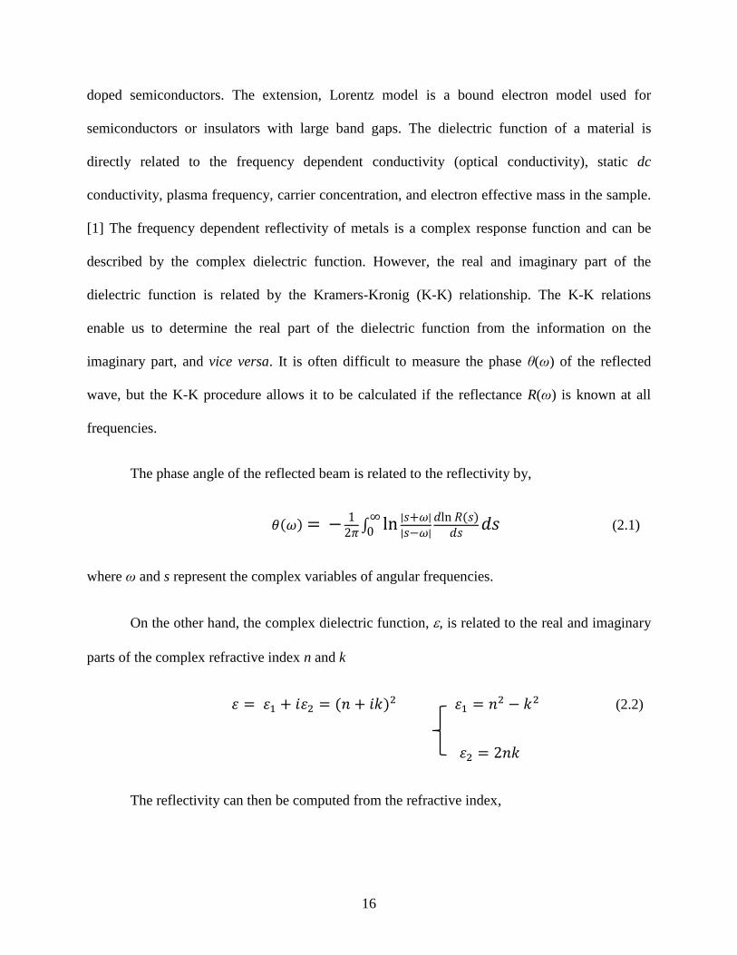
16
doped semiconductors. The extension, Lorentz model is a bound electron model used for
semiconductors or insulators with large band gaps. The dielectric function of a material is
directly related to the frequency dependent conductivity (optical conductivity), static dc
conductivity, plasma frequency, carrier concentration, and electron effective mass in the sample.
[1] The frequency dependent reflectivity of metals is a complex response function and can be
described by the complex dielectric function. However, the real and imaginary part of the
dielectric function is related by the Kramers-Kronig (K-K) relationship. The K-K relations
enable us to determine the real part of the dielectric function from the information on the
imaginary part, and vice versa. It is often difficult to measure the phase θ(ω) of the reflected
wave, but the K-K procedure allows it to be calculated if the reflectance R(ω) is known at all
frequencies.
The phase angle of the reflected beam is related to the reflectivity by,
𝜃(𝜔) = − 12𝜋
∫ ln |𝑠+𝜔|
|𝑠−𝜔|
∞0
𝑑ln 𝑅(𝑠)𝑑𝑠
𝑑𝑠 (2.1)
where ω and s represent the complex variables of angular frequencies.
On the other hand, the complex dielectric function, , is related to the real and imaginary
parts of the complex refractive index n and k
𝜀 = 𝜀1 + 𝑖𝜀2 = (𝑛 + 𝑖𝑘)2 𝜀1 = 𝑛2 − 𝑘2 (2.2)
𝜀2 = 2𝑛𝑘
The reflectivity can then be computed from the refractive index,
17
𝑅 = (𝑛−1)2
+𝑘2
(𝑛+1)2
+𝑘2 (2.3)
where the frequency dependent conductivity can then be evaluated from,
ɛ(𝜔) = 𝜀0 +4𝜋𝑖𝜎
𝜔 (2.4)
Finally the optical conductivity is related to the concentration of the charge carrier N.
𝜎(𝜔) = 𝑁𝑒2𝜏𝑚∗(1−𝑖𝜔𝜏)
(2.5)
When the frequency dependent optical conductivity is extrapolated to zero frequency
(ω→ 0) gives the dc conductivity of the material. Eq. 2.1-2.5 show that once the dielectric
function is known, the optical conductivity, σ, can be evaluated.
A common and useful feature in the reflectivity spectrum of a doped semiconductor is a
“dip” in the reflectivity spectrum known as the plasma reflection edge or plasma dip. [1]
According to the Drude model, for doped semiconductors, the energy at the energy minimum
(plasma frequency ωp) is related to the carrier concentration (N) and the lectron effective (m*),
ωp2 = Ne2/ɛɛ0m* where ɛ is the dielectric constant of the material, and ɛ0 is the vacuum
permittivity. Therefore, the effective mass (m*) of electrons in a doped semiconductor can be
extracted from the plasma frequency (ωp) provided the electron concentration (N) is known. This
latter quantity can be obtained from separate Hall coefficient measurement.
The mid-infrared reflectance spectra presented in this thesis were measured at the side-
station of the U2A beamline, National Synchrotron Radiation Facility, Brookhaven National
Laboratory. Powder samples were prepared and loaded into a stainless steel gasket placed

18
between two 300 µm culets of a Sintek mini type IIa diamond anvil cell. The spectra were
recorded on a Bruker Vertex 80v FTIR spectrometer and a Hyperion 2000 IR microscope
attached with a liquid nitrogen cooled HgCdTe detector. In order to make a thin film, we closed
the diamond anvil cell and pressed the two opposing faces with hand pressure, and then
recovered the flatten sample. Half of the sample was removed exposing the diamond face. IR
reflectance of the exposed diamond face was as the reference from the purpose of scaling the
measured reflectance to absolute unit. Then the IR reflectance of sample (~100 µm) was
measured. Spectral data were collected with a resolution of 4 cm-1 and accumulated for 512 scans.
The reflectance is converted to absolute reflectivity by normalization to the known
reflectance of the diamond substrate measured under identical experimental conditions. For a
linear system [2] the optical conductivity was obtained by Kramers-Kronig (K-K) analysis of
data obtained from normal incidence reflectivity measurements, and then fitted using a
variational K-K constrained dielectric function, as implemented in the RefFIT code The dc
conductivity is obtained from fitting the data to the Drude-Lorentz (DL) model and extrapolated
to zero frequency. To determine the quality of the fit, the sum of the squared difference between
observed and the fitted, divided by the expected data (χ2) was computed. There are four
adjustable parameters in the Drude-Lorentz model (equation 2.6). They are the high frequency
dielectric constant ɛ∞, plasma frequency ωp, the transverse frequency (eigenfrequency) ω0, and
the linewidth (scattering rate) γ, respectively. We set the transverse frequency ω0 to zero, since it
only describes the response of the unbound or free charge carriers of a metal and therefore not
needed in the analysis of semiconductors. [2]
ɛ(𝜔) = 𝜀∞ + ∑𝜔2
𝑝𝑖
𝜔2𝑜𝑖−𝜔2−𝑖𝛾𝑖𝜔
𝑖 (2.6)

19
In Equation 2.6, (ω) is the frequency dependent dielectric function, which can be
expressed as the absolute reflectivity according to Fresnel formula. [1] The Drude-Lorentz fits
were performed with the RefFIT code. In the Drude-Lorentz model, the Drude model is related
to the free electron, and the Lorentz term is related to dipole oscillators. The initial guesses of the
four parameters, the plasma frequency (ωp) was set to about 2000 cm-1, ω0 was fixed into zero
for metal and doped semiconductor, the high frequency dielectric constant (∞) was adjusted into
about 10, and the scattering rate (γ) was valued to 1000 cm-1. This is followed by several iterative
cycles until the difference in the calculated and computed reflectivity satisfied the convergence
criterion, i.e the total χ2 did not vary significantly during the last few iterations. [2] If the fit is
satisfactory, the optical conductivity is calculated and information on dc conductivity can be
determined.
Fig. 2.1 Infrared reflectivity spectra measurement of HBBO under different pressures. (The band
marble “Diamond” was undesirable contribution of the C-C stretch from the diamond anvils.)
2000 4000 6000 80000.0
0.1
0.2
0.3
0.4
0.5
Refl
ecti
vity
Frequency (cm-1
)
Pressure (GPa)
1.1
1.5
2.9
4.6
5.6
6.6
7.2
8.2
9.7
11.4
D
i
a
m
o
n
d
20
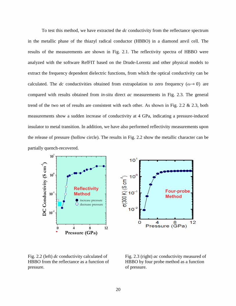
To test this method, we have extracted the dc conductivity from the reflectance spectrum
in the metallic phase of the thiazyl radical conductor (HBBO) in a diamond anvil cell. The
results of the measurements are shown in Fig. 2.1. The reflectivity spectra of HBBO were
analyzed with the software RefFIT based on the Drude-Lorentz and other physical models to
extract the frequency dependent dielectric functions, from which the optical conductivity can be
calculated. The dc conductivities obtained from extrapolation to zero frequency (ω→ 0) are
compared with results obtained from in-situ direct ac measurements in Fig. 2.3. The general
trend of the two set of results are consistent with each other. As shown in Fig. 2.2 & 2.3, both
measurements show a sudden increase of conductivity at 4 GPa, indicating a pressure-induced
insulator to metal transition. In addition, we have also performed reflectivity measurements upon
the release of pressure (hollow circle). The results in Fig. 2.2 show the metallic character can be
partially quench-recovered.
Fig. 2.2 (left) dc conductivity calculated of
HBBO from the reflectance as a function of
pressure.
Fig. 2.3 (right) ac conductivity measured of
HBBO by four probe method as a function
of pressure.
0 4 8 12
10-2
10-1
100
101
DC
Co
nd
ucti
vity
(S
cm
-1)
Pressure (GPa)
increase pressure
decrease pressure
Reflectivity Method
Four-probe Method

21
2.1.2 Infrared absorption spectra measurement
Infrared absorption spectrum can be used to determine the band gap of a semiconductor.
[3] For a direct band gap, the intensity (absorptivity) is proportional to the square root of the
photon energy. On the other hand, for indirect band the absorptivity is proportional to the square
of the photon energy. In addition, there is a contribution to the absorptivity associated with the
energy of the phonon that assist the electronic transition from the valence to the conduction band.
[4]
Experiments were performed at room temperature using mid infrared (560-8000cm-1)
radiation at IR beamline of the Canadian Light Source Inc. Typically a thin packed powder
sample ca. 100 µm was loaded on the diamond face of a 300 µm culets Sintek mini type IIa
diamond anvil cell. Spectra were recorded on a Hyperion 3000 IR microscope with a liquid
nitrogen cooled MCT detector. The IR spectrum of uncovered diamond surface was measured as
background. Spectrum was collected with an instrument resolution of 4 cm-1. For example, the
measured IR absorption spectrum of pure Mg2Si is shown in Fig. 2.4. The two arrows in the
spectrum show the energies for the creation and annihilation of a phonon associated with the
indirect gap excitation. (Fig. 2.4) The absorption feature indicates that the band gap is indirect. [4]
In this case, the mean value gives an indirect band gap energy of 0.65 eV and the estimated
phonon energy of 0.06 eV is comparable to the lattice vibration frequency of Mg2Si of 0.04 eV.
[4]

22
Fig. 2.4 Infrared absorption spectra of pure Mg2Si.
2.1.3 Synchrotron Powder X-ray diffraction measurements
Powder X-ray diffraction can be used to determine the crystal structure and obtain
information on the occupation and location of the dopant sites. Crystals are consisted of regular
arrays of atoms and when the wavelength of the X-ray is comparable to the interatomic distances
in the crystal, the phenomena of X-ray diffraction occurs. The basic principle of scattering of X-
ray in crystal is given by the Bragg’s Law: nλ=2dsinθ, where n is the order of reflection, λ is the
wavelength of incident ray; d is the interplanar spacing of the crystal; and θ is the angle of
incidence and the reflected X-ray (see Fig. 2.5). A diffraction pattern provides information on the
intensities and positions of the reflection Bragg peaks. A comparison of the Bragg peaks of the
diffraction patterns can reveal whether the dopants have changed the crystal structure of the host
Mg2Si.
Indirect Band Gap
23
Fig. 2.5 Bragg’s Law.
High resolution powder diffraction patterns were measured with synchrotron X-ray from
a bending magnet to monochromatized to 18 keV (0.68801 Å) using a double crystal
monochromator at the CMCF beamline of the Canadian Light Source. The diffraction patterns
were measured in the Debye-Scherrer configuration with an ACCEL MD2 micro-diffractometer
equipped with a MarMosaic mx300 CCD X-ray detector. LaB6 was used as the standard to
calibrate the sample to detector distance, tilt angle of detector, and the X-ray wavelength. The
program Fit2D V12.043 was used to convert 2D image of diffraction pattern into 1D profile.
Diffraction pattern with high energy (shorter wavelength) X-ray and including higher angle
diffraction peaks were measured at the HXMA beamline.
2.1.4 Maximum Entropy Method (MEM)
To characterize and better understand the effect of the dopants on the electron density
distribution in the host lattice of Mg2Si crystal, the maximum entropy analysis, which is known
to give qualitatively correct electron topology from X-ray diffraction pattern with a limited
number of Bragg reflections and without the knowledge of the atom positions, [5,8] were
performed.
The scattering intensity (I) is proportional to the square of structure factor (F) in Eq. 2.7.
𝐼 ∝ │𝐹│2 (2.7)

24
The structure factor (Fhkl) can provide the structure information of the sample and it can
be given by
𝐹ℎ𝑘𝑙 = ∑ 𝑔𝑖𝑖 𝑓𝑖(𝑑)𝑡𝑖𝑒𝑥𝑝[2𝜋𝑖(ℎ𝑥 + 𝑘𝑦 + 𝑙𝑧)] (2.8)
where (x, y, z) is atom position d is the d-spacing, gi is the site occupation factor for atom i, ti is
the temperature factor for atom i, and fi is the atomic scattering factor for atom i.
Another way to write the structure factor is consider atoms as a continuous distribution of
electron density at point (r). In this case, the expression of the structure factor (Fhkl) is the
function of electron density ρ (r).
𝐹ℎ𝑘𝑙 = ∫ 𝜌 (𝑟)𝑒𝑥𝑝[2𝜋𝑖(ℎ𝑥 + 𝑘𝑦 + 𝑙𝑧)]𝑑𝑉𝑢𝑛𝑖𝑡 𝑐𝑒𝑙𝑙
(2.9)
where h k l are Miller indices, x y z are the atomic positions, and V is the volume of unit cell.
From equation (2.9), the electron density ρ (r) is the Fourier transform of the structure
factors. Thus, the electron density ρ (r) can be extracted from Eq. 2.10.
𝜌(𝑥, 𝑦, 𝑧) =1
𝑉∑ 𝐹ℎ𝑘𝑙ℎ𝑘𝑙 𝑒𝑥𝑝[−2𝜋𝑖(ℎ𝑥 + 𝑘𝑦 + 𝑙𝑧)] (2.10)
Therefore, in principle electron density can be calculated from the structure factor by
Fourier transform. However, due to the incompleteness of diffraction information, this procedure
always suffer from series termination error and this created undesirable random background on
the extracted electron density.
The Maximum Entropy Method (MEM) of the information and probability theory is an
alternative way to extract the electron density. It was shown by Collins in 1982 electron density
distribution can be also calculated by using MEM from a limited diffraction data set. [5]

25
Compared to the traditional Fourier analysis, MEM avoid a series termination error. In this thesis,
due to the limited diffraction data sets obtained from powder diffraction, MEM is a useful way to
extract the electron densities of the doped samples.
The information entropy (S) is defined as
S = − ∑ 𝜌𝑖ln (𝜌𝑖
𝜏𝑖)𝑁
𝑖=1 (2.11)
where τi is normalized electron density at ith pixel derived from prior information. [6]
The unit cell is divided into N pixels of equal size and normalized electron density (ρi)
with each pixel considered as probability distribution of independent events.
The most probable electron density distribution in the unit cell is obtained by maximizing
the information entropy (S) subject to the following three constraints,
(𝑖) 𝜌𝑖 > 0 (2.12)
(𝑖𝑖) 𝐶𝐹 = ∑|𝐹𝑐 − 𝐹𝑜|2
𝜎𝑗2
= 𝑀𝐹
𝑀𝐹
𝑗=1
𝑎𝑛𝑑 (𝑖𝑖𝑖) ∑ 𝜌𝑖
𝑁
𝑖=1
= 1
where MF is the number of observed reflections, Fc and Fo are the calculated and observed
structure factors, respectively. σj is the estimated standard deviation in the observed structure
factor, and CF is defined as F-constraints.
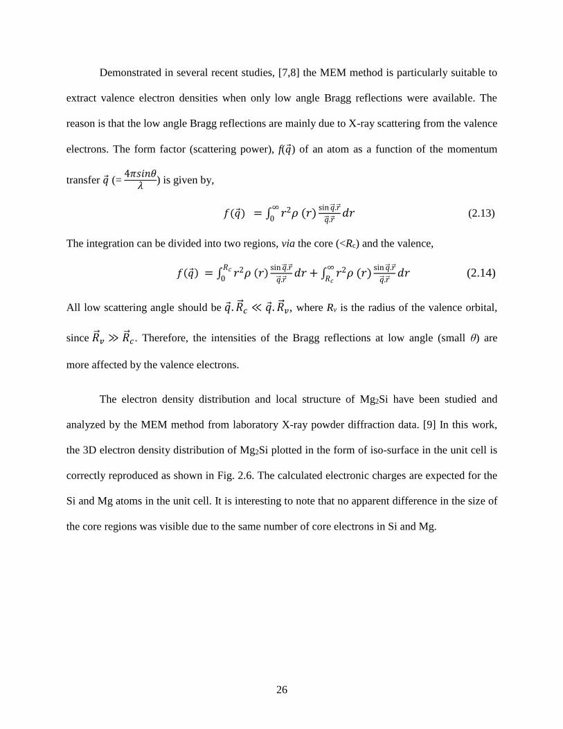
26
Demonstrated in several recent studies, [7,8] the MEM method is particularly suitable to
extract valence electron densities when only low angle Bragg reflections were available. The
reason is that the low angle Bragg reflections are mainly due to X-ray scattering from the valence
electrons. The form factor (scattering power), f(�⃗�) of an atom as a function of the momentum
transfer �⃗� (= 4𝜋𝑠𝑖𝑛𝜃
𝜆) is given by,
𝑓(�⃗�) = ∫ 𝑟2𝜌 (𝑟)∞
0
sin �⃗⃗⃗�.�⃗⃗�
�⃗⃗⃗�.�⃗⃗�𝑑𝑟 (2.13)
The integration can be divided into two regions, via the core (<Rc) and the valence,
𝑓(�⃗�) = ∫ 𝑟2𝜌 (𝑟)𝑅𝑐
0
sin �⃗⃗⃗�.�⃗⃗�
�⃗⃗⃗�.�⃗⃗�𝑑𝑟 + ∫ 𝑟2𝜌 (𝑟)
∞
𝑅𝑐
sin �⃗⃗⃗�.�⃗⃗�
�⃗⃗⃗�.�⃗⃗�𝑑𝑟 (2.14)
All low scattering angle should be �⃗�. �⃗⃗�𝑐 ≪ �⃗�. �⃗⃗�𝑣, where Rv is the radius of the valence orbital,
since �⃗⃗�𝑣 ≫ �⃗⃗�𝑐 . Therefore, the intensities of the Bragg reflections at low angle (small θ) are
more affected by the valence electrons.
The electron density distribution and local structure of Mg2Si have been studied and
analyzed by the MEM method from laboratory X-ray powder diffraction data. [9] In this work,
the 3D electron density distribution of Mg2Si plotted in the form of iso-surface in the unit cell is
correctly reproduced as shown in Fig. 2.6. The calculated electronic charges are expected for the
Si and Mg atoms in the unit cell. It is interesting to note that no apparent difference in the size of
the core regions was visible due to the same number of core electrons in Si and Mg.
27
Fig. 2.6 3D iso-surface of the electron density of Mg2Si in the unit cell superimposed on the
structure of Mg2Si. (Si atom is at the origin). The eight Mg atoms are seen inside the cubic unit
cell at ±(1/4 1/4 1/4).Figure taken from ref. [9]
In this thesis, the lattice parameters and the intensities of the Bragg reflections were
extracted from the diffraction patterns using the JANA 2006 software package by Le Bail fit.
The electron density distribution of the dopants in the crystal are then analyzed from the
diffraction patterns using the Maximum Entropy Method implemented in the “Dysnomia” code
[10].
2.2 Theoretical methods
First-principles computational electronic structure methods, based on laws of quantum
mechanics, are one of the most powerful research tools in physical sciences. In this thesis,
electronic structure calculations of thermoelectric materials are based on Density Function
Theory (DFT) [11-13], implemented in the Vienna ab initio Simulation Package (VASP) [14,
15]. The temperature dependent Seebeck coefficient S(T) relevant to the thermoelectric
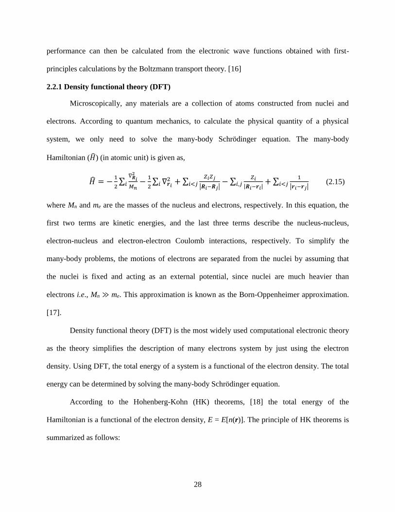
28
performance can then be calculated from the electronic wave functions obtained with first-
principles calculations by the Boltzmann transport theory. [16]
2.2.1 Density functional theory (DFT)
Microscopically, any materials are a collection of atoms constructed from nuclei and
electrons. According to quantum mechanics, to calculate the physical quantity of a physical
system, we only need to solve the many-body Schrödinger equation. The many-body
Hamiltonian (�̂�) (in atomic unit) is given as,
�̂� = −1
2∑
∇𝑹𝑖2
𝑀𝑛𝑖 −
1
2∑ ∇𝒓𝑖
2𝑖 + ∑
𝑍𝑖𝑍𝑗
|𝑹𝑖−𝑹𝑗|𝑖<𝑗 − ∑𝑍𝑖
|𝑹𝑖−𝒓𝑖|𝑖,𝑗 + ∑1
|𝒓𝑖−𝒓𝑗|𝑖<𝑗 (2.15)
where Mn and me are the masses of the nucleus and electrons, respectively. In this equation, the
first two terms are kinetic energies, and the last three terms describe the nucleus-nucleus,
electron-nucleus and electron-electron Coulomb interactions, respectively. To simplify the
many-body problems, the motions of electrons are separated from the nuclei by assuming that
the nuclei is fixed and acting as an external potential, since nuclei are much heavier than
electrons i.e., Mn ≫ me. This approximation is known as the Born-Oppenheimer approximation.
[17].
Density functional theory (DFT) is the most widely used computational electronic theory
as the theory simplifies the description of many electrons system by just using the electron
density. Using DFT, the total energy of a system is a functional of the electron density. The total
energy can be determined by solving the many-body Schrödinger equation.
According to the Hohenberg-Kohn (HK) theorems, [18] the total energy of the
Hamiltonian is a functional of the electron density, E = E[n(r)]. The principle of HK theorems is
summarized as follows:

29
The ground states energy of a system of interacting electrons is a unique functional of the
charge density. For a system with fixed number of electrons, the functional has its minimum
value for the correct ground state energy for variations in the charge density. [18]
The total energy functional of a many-electron system under an effective potential Veff in
atomic unit is given by,
𝑉𝑒𝑓𝑓(𝒓) = 𝑉𝑒𝑥𝑡(𝒓) + ∫𝑛(𝒓′)
|𝒓−𝒓′|𝑑3𝑟′ +
𝛿𝐸𝑥𝑐[𝑛(𝒓)]
𝛿𝑛(𝒓) (2.16)
where Vext (r) is the external potential due to the nuclei, the second term is the electron-density
interaction, and by the last term is the exchange-correlation.
A single particle Schrödinger equation (in atomic unit) is used to describe the interactions
of each individual electron with the mean field created by rest of the system is,
(−1
2∇2 + 𝑉𝑒𝑓𝑓(𝒓)) 𝜑𝑖(𝒓) = 𝜖𝑖𝜑𝑖(𝒓) (2.17)
where φi (r) is the single particle wave function.
The ground state total energy of a solid can be expressed in terms of a functional of the
electron density 𝑛(𝒓) and energy of nuclei,
𝐸𝑡𝑜𝑡𝑎𝑙[𝑛] = 𝐸𝑒𝑙𝑒𝑐𝑡𝑟𝑜𝑛[𝑛] + 𝐸𝑖𝑜𝑛 (2.18)
Applying the Born-Oppenheimer approximation, the ground state energy of an
interacting electron system is given by the Kohn-Sham equation (in atomic unit),
𝐸𝑒𝑙𝑒𝑐𝑡𝑟𝑜𝑛[𝑛(𝒓)] = 𝑇0[𝑛(𝒓)] +1
2∬
𝑛(𝒓)𝑛(𝒓′)
|𝒓−𝒓′|𝑑3𝑟𝑑3𝑟′ + ∫ 𝑉𝑒𝑥𝑡𝑛(𝒓)𝑑3𝑟 + 𝐸𝑥𝑐[𝑛(𝒓)] (2.19)
𝑇0[𝑛(𝒓)] = ∑ ∫ 𝑑3𝑟𝜑𝑖∗(𝒓)𝑖 (−
1
2∇2) 𝜑𝑖(𝒓). (2.20)
In the Kohn-Sham equation, the exchange correlation functional Exc [n(r)] is unknown. It
is essential to approximate the exchange and correlation energies by the electron density n(r),
and more accurately on the derivatives of the electron density ∇n(r). This method is known as
30
the generalized gradient approximation (GGA). [18] GGA has been demonstrated to be success
in many solid-states calculations with reliable results.
𝐸𝑥𝑐𝐺𝐺𝐴[𝑛] = ∫ 𝑑3𝑟𝑛(𝒓)𝜀𝑥𝑐
𝐺𝐺𝐴[𝑛, ∇𝑛] (2.21)
In the calculations, Blӧchl’s projector-augmented wave (PAW) potentials were used to
mimic the core electrons of the atoms. [19] The PAW potentials were constructed with the
Perdew-Burke-Ernzerhof (PBE) functional. [20]
2.2.2 Electronic structure calculation-Electronic density of states (DOS) and Projected
electronic density of states (PDOS)
The electronic density of states (DOS) of a solid is defined as number of electronic states
per unit volume per unit energy and is also a function that when multiplied by an interval of
energy. When the electronic density of states is projected to the atomic orbitals of the atoms
(PDOS), it can provide information on the contributions of the different orbitals to the electronic
states. The DOS and PDOS of a system are useful quantities to characterize the electronic
structure. Furthermore, the calculated DOS is essential to the input Seebeck coefficient
calculations. In this thesis, the electronic structure calculations were performed using density
functional theory (DFT) with the Perdew–Burke–Ernzerhof (PBE) generalized gradient
approximation (GGA) as implemented in the Vienna ab initio simulation package (VASP) code.
The projector-augmented wave (PAW) method, a real quantum potential, was adopted with 3s2
and 3s23p2 as valence electrons for the Mg and Si atoms.
2.2.3 GW approximation (GWA)
It is well known that the current GGA functional is not appropriate for the accurate
prediction of the band gap energy, due to the neglect of Coulomb repulsion and electron
correlation of the interacting electrons in the system. [21] GW approximation (GWA) has been

31
used to impose the electronic structure by including the effects of the electronic band structure.
In the GWA, G is the one-particle Green’s function and W is the screened Coulomb interaction.
[22-25] The GWA method was employed to calculate accurate band gap energy of pure Mg2Si at
ambient and high pressure.
2.2.4 Temperature dependent Seebeck coefficient S(T) calculation
The Seebeck coefficient can be calculated from the density of states obtained in the
electronic structure calculation using the VASP code with the V2Boltz program. [26] This
program computed the temperature dependent Seebeck coefficient S(T) for n-doped Mg2Si-based
thermoelectric materials within the rigid band approximation based on the semi-classical
Boltzmann transport theory with the DOS as the only input.
The electrical conductivity σ0(T) of a solid can be calculated from the band structure by
the energy integral, [27]
𝜎0(𝑇) =𝑒2
3ℏ∫ [−
𝜕𝑁(𝐸)
𝜕𝐸] 𝑁(𝐸)𝜈2(𝐸)𝜏(𝐸, 𝑇)𝑑𝐸 (2.22)
where e, τ, N, and ν are electron charge, electronic relaxation time, electron density of states, and
Fermi velocity, respectively.
The temperature dependent Seebeck coefficient S(T) is the ratio of the 0th and 1st moment
of the integral,
𝑆(𝑇) =1
𝑒𝑇
𝐼1
𝐼0 (2.23)
where 𝐼𝑥(𝑇) = ∫ [−𝜕𝑁(𝐸)
𝜕𝐸] 𝑁(𝐸)𝜈2(𝐸)𝜏(𝐸, 𝑇)(𝐸 − 𝐸𝐹)𝑥𝑑𝐸, and EF is the Fermi energy.
Inspection of Eq. 2.23 shows a high efficient thermoelectric material should have a high
electronic density of states near the Fermi level and a reasonable electrical conductivity. The
temperature dependent Seebeck coefficient S(T) of the doped Mg2Si sample can be estimated
32
from the ground state band structure using the rigid band model by shifting the energy of the
Fermi level according to the number of electrons donated by the dopant. Thus, an ideal
thermoelectric material with the large predicted Seebeck coefficient at low doping concentration
will have a high Fermi velocity and high electron density of states (DOS) at the Fermi energy.
Generally a high DOS indicates the electron band dispersions near the Fermi level must be fairly
flat. [27]
References
[1] M. Fox, Optical Properties of Solids, Oxford University Press, New York City, NY, USA,
2010.
[2] A. B. Kuzmenko, Rev. Sci. Instrum., 2005, 76, 083108.
[3] A. Akrap, M. Tran, A. Ubaldini, J. Teyssier, E. Giannini, and D. V. D. Marel, Physical
Review B, 2012, 86, 235207.
[4] W. B. Whitten, P. L. Chung, and G. C. Danielson, Journal of Physics and Chemistry of
Solids, 1965, 26, 49-56.
[5] D. M. Collins, Nature, 1982, 298, 49-51.
[6] C. J. Gilmore, Acta Cryst. A, 1996, 52, 561-589.
[7] J. S. Tse, M. Hanfland, R. Flacau, S. Desgreniers, Z. Li, K. Mende, K. Gilmore, A. Nyrow,
M. M. Sala, and C. Sternemann, J. Phys. Chem. C., 2014, 118, 1161-1166.
[8] R. Li, J. Liu, L. Bai, J. S. Tse, and G. Shen, Applied Physics Letters, 2015, 107, 072109.
[9] R. Saravanan and M. C. Robert, Journal of Alloys and Compounds, 2009, 479, 26-31.
[10] K. Momma, T. Ikeda, A. A. Belik and F. Izumi, Powder Diffraction, 2013, 28, 184-193.
[11] P. Hohenberg and W. Kohn, Phys. Rev. B, 1964, 136, B864.
[12] W. Kohn and L. J. Sham, Phys. Rev., 1965, 140, A1133.
[13] I. Gilbert, Phys. Rev. B, 1975, 1, 2112.
[14] G. Kresse and J. Furthmüller, Computational Materials Science, 1996, 6, 15-50.

33
[15] G. Kresse and J. Furthmüller, Phys. Rev. B, 1996, 54, 11169.
[16] G. K. H. Madsen and D. J. Singh, Computer Physics Communications, 2006, 175, 67-71.
[17] M. Born and R. Oppenheimer, Annalen der Physik, 1927, 389, 457-484..
[18] J. P. Perdew, K. Burke, and M. Ernzerhof, Phys. Rev. Lett., 1996, 77, 3865-3868.
[19] P. E. Blöchl, Phys. Rev. B, 1994, 50, 17953.
[20] G. Kresse and D. Joubert, Phys. Rev. B, 1999, 59, 1758.
[21] L. J. W. Aulbur and J. Wilkins, Solid State Physics, 2000, 54, 1.
[22] L. Hedin, Phys. Rev., 1965, 139, A796–A823.
[23] P. Garcia–Gonzalez and R. W. Godby, Phys. Rev. B, 2011, 63, 075112.
[24] F. Aryasetiawan and O. Gunnarsson, Physical Review Letters, 1995, 74, 3221.
[25] S. V. Faleev, M. V. Schilfgaarde, and T. Kotani, Physical Review Letters, 2004, 93,
126406.
[26] M. Chen, in First-principles Modeling of Thermoelectric Materials, PhD thesis,
Theoretical Solid State Chemistry, Vienna University of Technology, Vienna, Austria,
2012.
[27] J. S. Tse and D. D. Klug, “Thermoelectrics Handbook: Macro to Nano,” ed. D.M. Rowe,
CRC Press.
34
CHAPTER 3
Sb- AND Bi- DOPED Mg2Si: LOCATION OF THE DOPANTS, MICRO- AND
NANOSTRUCTURES, ELECTRONIC STRUCTURES AND THERMOELECTRIC
PROPERTIES
Although the potential of Mg2Si as a thermoelectric material was recognized in 1961,
[11] systematic optimization of its properties only began in the last decade. The Mg2Si-based
materials composed of non-toxic, abundant and affordable elements are very attractive for large-
scale industrial applications. Previous researches have focused on replacing the Si site with Ge
and/or Sn to lower its thermal conductivity, or by doping with Sb or Bi. Unfortunately, despite
substantial efforts, the thermoelectric performance remains relatively low. For example, ball-
milled and hot-pressed as well as spark-plasma-sintered (SPS) Bi-doped Mg2Si has been reported
to reach ZTmax = 0.7~0.86 at around 800 K. [12,13] Unfortunately, a significant amount of
Mg3Bi2, an undesirable side product after SPS, was always present. [14] Further improvement
has been achieved by multiple doping. For example, Sb-doped Mg2Si0.4Sn0.6 has attained a ZTmax
= 1.1 at 800 K, [16] and melt-spinning of Mg2Si0.4Sn0.6Bi0.03 followed by SPS has improved it to
a ZTmax = 1.2 at 573 K. [17]
This chapter presents results of the characterization of Mg2Si-based thermoelectric
materials by adding single dopants, Sb or Bi, to Mg2Si. The compounds studied were
Mg2Si0.98Sb0.02 and Mg2Si0.98Bi0.02. The dc conductivities of the doped samples were extracted
from the analysis of infrared (IR) reflectivity spectra employing the Drude free electron model.
We found infrared (IR) measurements of the dc conductivity systematically lower than the in-
situ four probe measurements of the bulk sample because of the limited penetration depth and
very small spot size of the IR radiation. The electron effective masses in the samples were also
extracted from the “plasma dip” according to the procedure described in equations 2.1-2.5 of

35
Chapter 2. Furthermore, the band gap of undoped Mg2Si as determined by infrared absorption
spectrum was found to be indirect with a gap energy of 0.65 eV. This result is in excellent
agreement with previous studies. [31-35] To help explain the experimental observation, the
electron densities of states of Sb- and Bi-doped Mg2Si were calculated with the DFT method.
The most significant observation is that, even with localized defect atoms (i.e. Sb or Bi),
electrons donated by the dopants were delocalized over the entire crystal and did not appear as a
localized band between the energy gap of Mg2Si. This observation confirms the validity of the
rigid band approximation used by shifting the Fermi level according to the number of electrons
donated by the dopant in the calculation of the Seebeck coefficients using the semiclassical
Boltzmann transport theory. The calculations predicted negative Seebeck coefficients for the
doped samples, consistent with the consequence of n-doping. The absolute magnitude of Seebeck
coefficients was found to decrease with the dopant concentration. Experimentally, the highest
absolute value of Seebeck coefficient was found to be -170 µVK-1 at 800 K for Mg2Si0.99Sb0.01
and the highest ZT = 0.6 at 700 K was achieved for Mg2Si0.98Bi0.02.
The results of this study have been published in
N. Farahi, M. VanZant, J. Zhao, J. S. Tse, S. Prabhudev, G. A. Botton, J. R. Salvador, F.
Borondics, Z. Liu and H. Kleinke, “Sb- and Bi- doped Mg2Si: location of the dopants, micro-
and nanostructure, electronic structures and thermoelectric properties,” Dalton Transactions, vol.
43, pp. 14983-14991, 2014.
The authors’ contributions are as follows:
N. Farahi, M. VanZant and H. Kleinke synthesized the samples and performed the
thermoelectric property measurements.

36
J. Zhao and J. S. Tse performed infrared absorption and reflectivity measurements,
performed analysis to extract the dielectric functions and transport properties, and
computed the electronic structures and Seebeck coefficients.
S. Prabhudev and G. A. Botton performed the STEM measurement.
J. R. Salvador performed the Hall measurement.
F. Borondics and Z. Liu assisted in performing infrared experiments at CLS and BNL,
respectively.
All authors contributed to the writing and editing of the manuscript.
Abstract
Due to increasing global energy concerns, alternative sustainable methods to create
energy such as thermoelectric energy conversion have become increasingly important.
Originally, research into thermoelectric materials was focused on tellurides of bismuth and lead
because of the exemplary thermoelectric properties of Bi2Te3 and PbTe. These materials,
however, contain toxic lead and tellurium, which is also scarce and thus expensive. A viable
alternative material may exist in Mg2Si, which needs to be doped and alloyed in order to achieve
reasonable thermoelectric efficiency. Doping is a major problem, as p-type doping has thus far
not produced competitive efficiencies, and n-type doping is problematic because of the low
solubility of the typical dopants Sb and Bi. This investigation shows experimentally that these
dopants can indeed replace Si in the crystal lattice, and excess Sb and Bi atoms are present in the
grain boundaries in the form of Mg3Sb2 and Mg3Bi2. As a consequence, the carrier concentration
is lower than the formal Sb/Bi concentration suggests, and the thermal conductivity is
significantly reduced. DFT calculations are in good agreement with the experimental data,

37
including the band gap and the Seebeck coefficient. Overall, this results in competitive
efficiencies despite the low carrier concentration. While ball-milling was previously shown to
enhance the solubility of the dopants and thus the carrier concentration, this did not lead to
enhanced thermoelectric properties.
3.1 Introduction
Thermoelectric energy conversion is receiving increasing attention, while the global
energy resources are declining. Thermoelectric (TE) materials can generate electricity out of heat
(more precisely: out of a temperature gradient), which may be used to turn waste heat into useful
electrical energy, such as in automotives. [1] The thermoelectric conversion efficiency increases
with increasing thermoelectric figure of merit, defined as ZT = TS2σκ−1. Therein, S is the Seebeck
coefficient, σ the electrical conductivity, κ the thermal conductivity, and T the absolute
temperature. This figure of merit needs to be improved to enhance the conversion efficiency, as
is required for this technology to become economically viable, for example in automotives.
Typically, heavy metal tellurides and antimonides dominate the best thermoelectric
materials, including materials based on doped Bi2Te3, [2,3] PbTe, [4-6] Tl9SbTe6 [7] and
Tl9BiTe6, [8] La0.4Yb13.6MnSb11, [9] and skutterudites including Ba0.08La0.05Yb0.04- Co4Sb12. [10]
While using these heavy materials has its advantages, most notably the high figure of merit, in
excess of unity, in part related to low thermal conductivity, three serious problems are associated
with using tellurium, antimony, lead, thallium and lanthanides in large-scale applications. These
problems are toxicity, availability, and cost. Therefore, alternative materials comprised of non-
toxic, abundant and affordable elements are very attractive, though they may end up being less
efficient. From this point of view, Mg2Si - adopting the anti-fluorite structure type - appears as a
perfect candidate. While its potential as a thermoelectric was already discussed in 1961, [11]
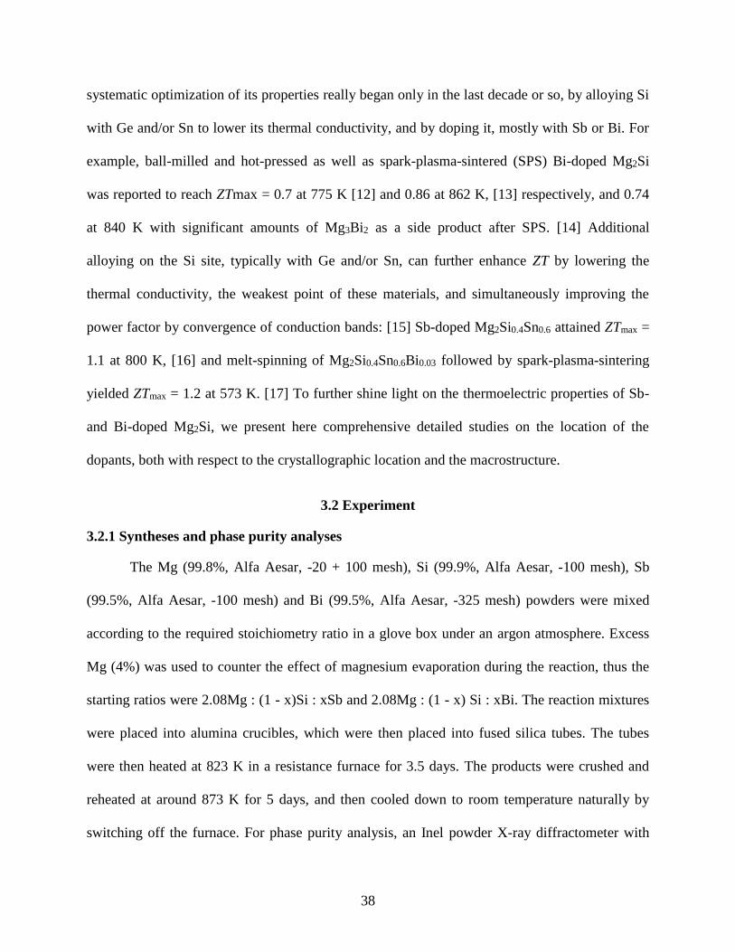
38
systematic optimization of its properties really began only in the last decade or so, by alloying Si
with Ge and/or Sn to lower its thermal conductivity, and by doping it, mostly with Sb or Bi. For
example, ball-milled and hot-pressed as well as spark-plasma-sintered (SPS) Bi-doped Mg2Si
was reported to reach ZTmax = 0.7 at 775 K [12] and 0.86 at 862 K, [13] respectively, and 0.74
at 840 K with significant amounts of Mg3Bi2 as a side product after SPS. [14] Additional
alloying on the Si site, typically with Ge and/or Sn, can further enhance ZT by lowering the
thermal conductivity, the weakest point of these materials, and simultaneously improving the
power factor by convergence of conduction bands: [15] Sb-doped Mg2Si0.4Sn0.6 attained ZTmax =
1.1 at 800 K, [16] and melt-spinning of Mg2Si0.4Sn0.6Bi0.03 followed by spark-plasma-sintering
yielded ZTmax = 1.2 at 573 K. [17] To further shine light on the thermoelectric properties of Sb-
and Bi-doped Mg2Si, we present here comprehensive detailed studies on the location of the
dopants, both with respect to the crystallographic location and the macrostructure.
3.2 Experiment
3.2.1 Syntheses and phase purity analyses
The Mg (99.8%, Alfa Aesar, -20 + 100 mesh), Si (99.9%, Alfa Aesar, -100 mesh), Sb
(99.5%, Alfa Aesar, -100 mesh) and Bi (99.5%, Alfa Aesar, -325 mesh) powders were mixed
according to the required stoichiometry ratio in a glove box under an argon atmosphere. Excess
Mg (4%) was used to counter the effect of magnesium evaporation during the reaction, thus the
starting ratios were 2.08Mg : (1 - x)Si : xSb and 2.08Mg : (1 - x) Si : xBi. The reaction mixtures
were placed into alumina crucibles, which were then placed into fused silica tubes. The tubes
were then heated at 823 K in a resistance furnace for 3.5 days. The products were crushed and
reheated at around 873 K for 5 days, and then cooled down to room temperature naturally by
switching off the furnace. For phase purity analysis, an Inel powder X-ray diffractometer with

39
Cu-Kα1 radiation and a position sensitive detector was used. For x = 0.02, the samples appeared
to contain only Mg2Si1−xSbx and Mg2Si1−xBix, respectively, with traces of MgO, i.e. no unreacted
Si, Sb or Bi were detected. Larger amounts of Sb or Bi resulted in noticeable formation of
Mg3Sb2 or Mg3Bi2.
Additional powder X-ray diffraction experiments on Mg2Si and Mg2Si0.98Bi0.02 were
performed at the CMCF-II beamline at the Canadian Light Source. Synchrotron radiation from a
bending magnet port was monochromatized to 18 keV (0.68801 Å) with a double crystal
monochromator and focused to the sample with a toroidal mirror. Powder diffraction patterns
were measured in the Debye–Scherrer configuration with a versatile ACCEL MD2 micro-
diffractometer and MarMosaic mx300 CCD X-ray detector. These experiments confirmed the
results obtained from the Inel diffractometer, and showed evidence of a small unit cell expansion
upon doping with Bi, namely from a = 6.33504(5) Å to a = 6.34227(6) Å, as shown in Fig. A.1
in the ESI.
To investigate the microstructure homogeneity of the samples, energy dispersive X-ray
(EDX) analysis was performed on a piece of the hot-pressed pellets using a Zeiss ULTRA plus
electron microscope associated with an EDX device, EDAX Pegasus 1200. The EDX results
confirmed the existence of Sb and Bi in the samples with some Sb- and Bi-rich regions,
respectively; the analysis of different crystals resulted in an average ratio of 2.05Mg : 0.94Si :
0.01Bi.
Differential scanning calorimetry (DSC) was used to examine the thermal stability of the
samples with x = 0.02. The DSC measurement was performed under argon flow by using the
NETZSCH STA 409PC Luxx instrument with a heating rate of 10 K min−1 from 300 K to 1073

40
K. No phase transition was detected, and the weight loss was <2%, possibly within experimental
error. The plots are presented in Fig. A.2 in the ESI.
3.2.2 Transmission electron microscopy
Atomic-scale structural characterization and elemental analyses were performed using
scanning transmission electron microscopy (STEM) operating in a high-angle annular dark-field
imaging (HAADF) mode and energy dispersive X-ray Spectrometry (XEDS). Conventional
TEM is primarily a broad-beam based technique, wherein all the scattered electrons, upon
interacting with the specimen, are collected over a large illumination area on the specimen. In
these conditions, images are strongly dependent on the thickness of the sample and objective
lens-focus conditions. As opposed to this, STEM-HAADF employs a raster scanning electron
probe to collect electrons that are elastically scattered at high angles. Upon converging the
electron beam into a sub-angstrom probe, an atomic-scale image of materials can be obtained.
The high angle annular dark field (HAADF) detector, as the name suggests, is a detector
designed with an annular geometry and placed in a diffraction plane below the sample so as to
collect electrons emerging from the specimen at high scattering angles. Since the intensity of
these high-angle scattered electrons is directly related to the atomic number of scattering atoms
under the electron beam, the resulting STEM-HAADF image provides an atomic number “Z”-
contrast image with intensities proportional to Z1.6. For instance, in the case of the Mg2Si sample
doped with Bi, the atomic columns containing Bi (Z = 83) are expected to appear significantly
brighter compared to the bulk of the matrix crystal.
Atomically-resolved STEM-HAADF images were acquired using a FEI-Titan cubed
TEM, equipped with two hexapole-design spherical aberration correctors of the probe and image
forming lenses. The microscope was operated in the STEM mode at an accelerating voltage of

41
300 kV and the images were acquired using a Fischione Instruments HAADF detector. Image
simulations were carried out using the multislice method by implementing the Kirkland code
[18] in order to validate the structural model and deductions of the dopant site preference.
For STEM characterization, the samples were thinned by mechanical polishing to 180 μm
thickness, then dimple-ground with a diamond paste to a central thickness of 20 μm and finally
ion milled (using a Gatan PIPS model) to electron transparency.
3.2.3 Electronic structure calculations
The electronic structure calculations were performed using density functional theory
(DFT) with the Perdew-Burke-Ernzerhof (PBE) generalized gradient approximation (GGA) [19]
as implemented in the Vienna ab initio simulation package (VASP) code. [20-23] To obtain a
more accurate band gap, additional calculations were performed via the GW approximation
(GWA), which utilizes the one-particle Green’s function and the screened Coulomb interaction
W. [24,25] For the GGA calculation, the projector-augmented wave (PAW) [26,27] method was
adopted with 2p63s2 and 3s23p2 as valence electrons for the Mg and Si atoms, respectively. An
energy cut-off of 332 eV and an appropriate Monkhorst-Pack scheme was employed for the
Brillouin zone with a dense k-mesh of 25 × 25 × 25 for the Seebeck coefficient calculation. The
band structure was calculated with the VASP code with a 16 × 16 × 16 k-point set. For doping
with Sb and Bi, a 2 × 2 × 2 supercell was created from the Mg2Si crystal structure, where one out
of 32 Si atoms was replaced either with an Sb or a Bi atom. The stoichiometry of the doped
model is thus approximately Mg2Si0.97Pn0.03 (Pn = Sb, Bi). For the Bi case, spin–orbit coupling
was included in the calculation. By using VASP output and symmetry, the V2Boltz program [28]
was applied on the basis of semiclassical Boltzmann transport theory to calculate the temperature

42
dependent Seebeck coefficient S(T) for n-doped Mg2Si-based thermoelectric materials within the
rigid band approximation. [29]
3.2.4 Physical property measurements
To verify the band gap, an infrared transmission spectrum was obtained from a ground
sample of undoped Mg2Si at room temperature using a Fourier transform IR spectrometer,
utilizing the Mid Infrared (560-8000 cm−1) Spectromicroscopy beamline at the Canadian Light
Source Inc. The sample was loaded on the 300 μm culets of a Sintek mini type IIa diamond anvil
cell. The spectra were recorded on a Hyperion 3000 IR microscope with a liquid nitrogen cooled
MCT detector. For the measurement, the diamond was firstly measured as a background
spectrum. After extracting the background, the sample of ∼100 μm was focused by microscopy
and measured. Spectral data collection employed a resolution of 4 cm−1 and 512 scans.
The mid- and far-infrared reflectance spectra of undoped Mg2Si and Mg2Si doped with Bi
or Sb were measured at the National Synchrotron Radiation Facility, Brookhaven National
Laboratory. The sample preparation procedure was the same as described above. Far-infrared
reflectivity experiments were performed at the side-station of the U2A beamline. Mid-infrared
reflectivity was measured with a Bruker Vertex 80v FTIR spectrometer and a Hyperion 2000 IR
microscope attached to a liquid nitrogen cooled HgCdTe detector. A conventional globar source
was used to minimize any intensity fluctuation during the measurements. The intensity of the
source was calibrated against the synchrotron ring current using a gold foil. A KBr beam splitter
was used to cover the mid-IR region, and the spectral resolution of 4 cm−1 applied to all spectra.
The reflectance was converted to absolute reflectivity by normalization to the reflectance
diamond substrate measured under identical experimental conditions. Optical conductivity was
43
obtained by Kramers-Kronig (K-K) analysis of data obtained from normal incidence reflectivity
measurements, then fit using a variational K-K constrained dielectric function, as implemented in
the REFFIT code. [30] The dc conductivity is obtained from fitting to the Drude model and
extrapolated to zero frequency. Since the mid and far-infrared spectra were recorded on different
detectors, the reflectances in the two regions were connected manually by matching to the mid-
infrared reflectance at 600 cm−1 (0.75 eV).
The doped Mg2Si samples were ground and then consolidated in an argon atmosphere
under a pressure of 32 MPa at 973 K by using an Oxy-Gon hot press to obtain a cylindrical pellet
of 12.7 mm diameter and 3 mm thickness. The pressure was released after heating for 2 hours to
eliminate strain on the pellets during the cool-down procedure. Thermal diffusivity (α)
measurements were performed on the polished pressed samples under argon flow by using an
Anter Flashline FL3000 thermal properties analyzer between 350 K and 670 K. For calculating
the thermal conductivity (κ), the density (d) of the pellets was measured via the Archimedes
method, and the Dulong–Petit approximation was applied for determining specific heat (CP)
values. The thermal conductivity was then calculated according to κ = αdCP.
Rectangular bars with dimensions of approximately 10 × 2 × 2 mm, cut from the same
hot-pressed pellets, were used for electrical conductivity (σ) and Seebeck coefficient (S)
measurements. These measurements were performed simultaneously under a helium atmosphere
by using the ULVAC-RIKO ZEM-3 apparatus between 300 K and 800 K.
The Hall measurements were recorded from 5 K to 300 K using a cryostat equipped with
a 5 T magnet and a linear research AC resistance bridge. Ohmic contacts were made by using

44
silver paint. The Hall mobility, μH, was calculated from the relation μH = σn−1e−1, where n =
carrier concentration and e = electron charge.
3.3 Results and discussion
3.3.1 Micro- and nanostructure
Low-magnification TEM imaging revealed the polycrystalline nature of the sample with
grain sizes of the order of 7 μm. We did not observe any formation of Bi-rich precipitates in the
matrix. Additionally, STEM-HAADF characterization was performed at an atomic resolution to
locate the doped Bi atoms. The principal regions of interest included the bulk of the sample, and
the grain boundaries. Fig. 3.1a shows the atomic-resolution STEM-HAADF image from the bulk
of the Mg2Si0.98Bi0.02 sample, oriented along the [110] zone axis. A significant number of atomic
columns with brighter intensity are distributed randomly over the lattice. Due to the Z-
dependence in these imaging conditions, we infer that these bright atomic columns correspond to
columns containing Bi dopant atoms located on the original Si atoms, deduced from the image
simulations discussed further below. The relative variation in the intensities among the bright
atomic columns indicates that these columns could contain single Bi dopants or possibly more Bi
atoms. However, due to the lack of information on the location of the Bi atoms in the thickness
of the sample, we cannot extract further quantitative information on the number of atoms within
one column due to the sensitivity of the image intensity upon the precise location of the
scattering atoms.
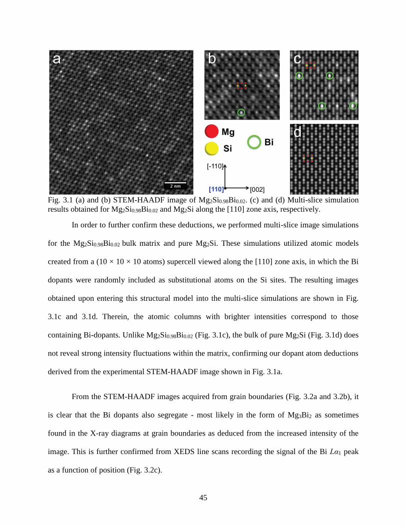
45
Fig. 3.1 (a) and (b) STEM-HAADF image of Mg2Si0.98Bi0.02. (c) and (d) Multi-slice simulation
results obtained for Mg2Si0.98Bi0.02 and Mg2Si along the [110] zone axis, respectively.
In order to further confirm these deductions, we performed multi-slice image simulations
for the Mg2Si0.98Bi0.02 bulk matrix and pure Mg2Si. These simulations utilized atomic models
created from a (10 × 10 × 10 atoms) supercell viewed along the [110] zone axis, in which the Bi
dopants were randomly included as substitutional atoms on the Si sites. The resulting images
obtained upon entering this structural model into the multi-slice simulations are shown in Fig.
3.1c and 3.1d. Therein, the atomic columns with brighter intensities correspond to those
containing Bi-dopants. Unlike Mg2Si0.98Bi0.02 (Fig. 3.1c), the bulk of pure Mg2Si (Fig. 3.1d) does
not reveal strong intensity fluctuations within the matrix, confirming our dopant atom deductions
derived from the experimental STEM-HAADF image shown in Fig. 3.1a.
From the STEM-HAADF images acquired from grain boundaries (Fig. 3.2a and 3.2b), it
is clear that the Bi dopants also segregate - most likely in the form of Mg3Bi2 as sometimes
found in the X-ray diagrams at grain boundaries as deduced from the increased intensity of the
image. This is further confirmed from XEDS line scans recording the signal of the Bi Lα1 peak
as a function of position (Fig. 3.2c).
46
Fig. 3.2 (a) Atomic-resolution STEM-HAADF image of Mg2Si0.98Bi0.02 demonstrating Bi
segregation at the grain boundary (GB). (b) STEM-HAADF image acquired from the region
marked in yellow in (a). (c) EDX line-scan for Bi (red) over the same area marked in yellow.
3.3.2 Electronic structure
The densities of states calculated via the GGA vs. the GW approach are depicted in Fig.
3.3 (left). In each case, a narrow gap separates the valence band, mostly comprising Si-p states
from the conduction band, dominated by Mg states. The use of the screening correction (GW) did
not change the valence band, but shifted the empty states uniformly towards higher energies. As
a result, the calculated band gap increased from 0.2 eV to 0.67 eV, ultimately in agreement with
experimental data. [31] The band structures are shown in Fig. A.3 (ESI), revealing the indirect
band gap. Similarly, a computed (indirect) band gap of 0.6 eV [32] was obtained after employing
the modified Becke–Johnson local density functional (mBJLDA), [33,34] and applying the GW
corrections to selected k-points yielded a computed gap of 0.65 eV. [35]

47
The IR transmission spectrum of undoped Mg2Si is shown in Fig. 3.3 (right). The two
arrows in the IR transmission spectrum indicate energies of creation and annihilation of a phonon
associated with the gap excitation. The sloping feature of the transmittance indicates that the
band gap is indirect with an energy of 0.65 eV, confirming the results of the GW modified DFT
calculations discussed above. The phonon energy is estimated to be 0.06 eV. This can be
compared to the maximum IR absorption frequency of a lattice vibration of Mg2Si of 0.04 eV.
Fig. 3.3 Density of states (left) and absorbance spectrum (right) of Mg2Si.
The densities of states of Sb- and Bi-doped Mg2Si are compared in Fig. 3.4. The
composition is Mg64Si31Pn (Pn = Sb, Bi), which corresponds to Mg2Si0.97Pn0.03, i.e. a 3% doping
level of Pn on the Si site. The total densities of states for both systems are very similar to that of
pure Mg2Si shown in Fig. 3.3. The most significant observation is that, even with a localized
defect atom (i.e. Sb or Bi), the density of states projected to the Pn states shows that the electrons
from the dopant are spread over the entire crystal and are not localized in the region of the band
gap. This observation confirms that one can apply the rigid band approximation for calculating
the Seebeck coefficient. The relatively sharp peaks below -5 eV can be attributed to the
interaction between the Pn atoms and the surrounding Mg and Si atoms. At a 3% dopant
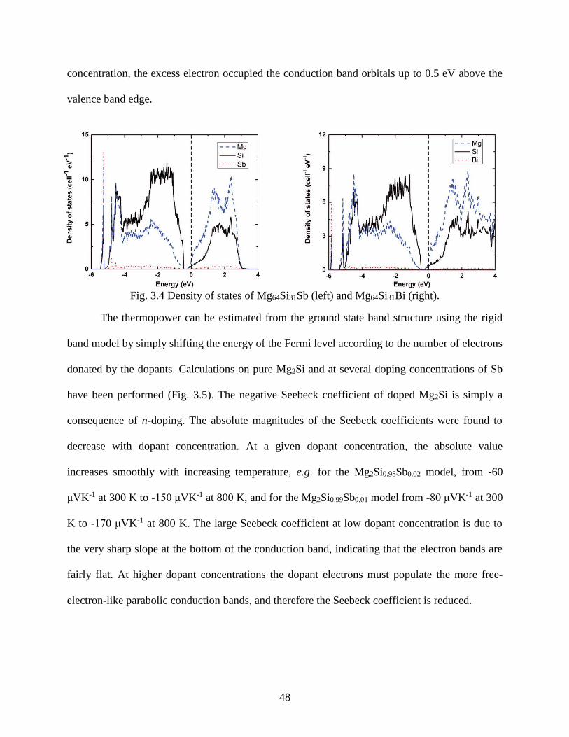
48
concentration, the excess electron occupied the conduction band orbitals up to 0.5 eV above the
valence band edge.
Fig. 3.4 Density of states of Mg64Si31Sb (left) and Mg64Si31Bi (right).
The thermopower can be estimated from the ground state band structure using the rigid
band model by simply shifting the energy of the Fermi level according to the number of electrons
donated by the dopants. Calculations on pure Mg2Si and at several doping concentrations of Sb
have been performed (Fig. 3.5). The negative Seebeck coefficient of doped Mg2Si is simply a
consequence of n-doping. The absolute magnitudes of the Seebeck coefficients were found to
decrease with dopant concentration. At a given dopant concentration, the absolute value
increases smoothly with increasing temperature, e.g. for the Mg2Si0.98Sb0.02 model, from -60
μVK-1 at 300 K to -150 μVK-1 at 800 K, and for the Mg2Si0.99Sb0.01 model from -80 μVK-1 at 300
K to -170 μVK-1 at 800 K. The large Seebeck coefficient at low dopant concentration is due to
the very sharp slope at the bottom of the conduction band, indicating that the electron bands are
fairly flat. At higher dopant concentrations the dopant electrons must populate the more free-
electron-like parabolic conduction bands, and therefore the Seebeck coefficient is reduced.
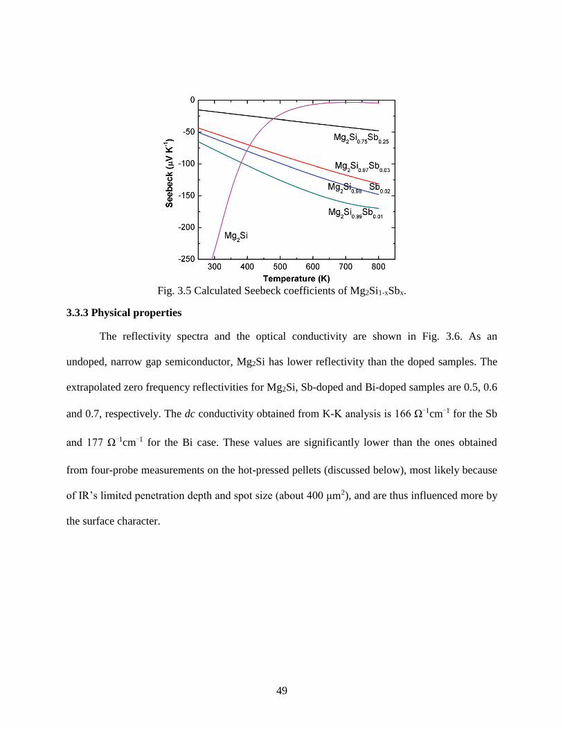
49
Fig. 3.5 Calculated Seebeck coefficients of Mg2Si1-xSbx.
3.3.3 Physical properties
The reflectivity spectra and the optical conductivity are shown in Fig. 3.6. As an
undoped, narrow gap semiconductor, Mg2Si has lower reflectivity than the doped samples. The
extrapolated zero frequency reflectivities for Mg2Si, Sb-doped and Bi-doped samples are 0.5, 0.6
and 0.7, respectively. The dc conductivity obtained from K-K analysis is 166 Ω-1cm-1 for the Sb
and 177 Ω-1cm-1 for the Bi case. These values are significantly lower than the ones obtained
from four-probe measurements on the hot-pressed pellets (discussed below), most likely because
of IR’s limited penetration depth and spot size (about 400 μm2), and are thus influenced more by
the surface character.
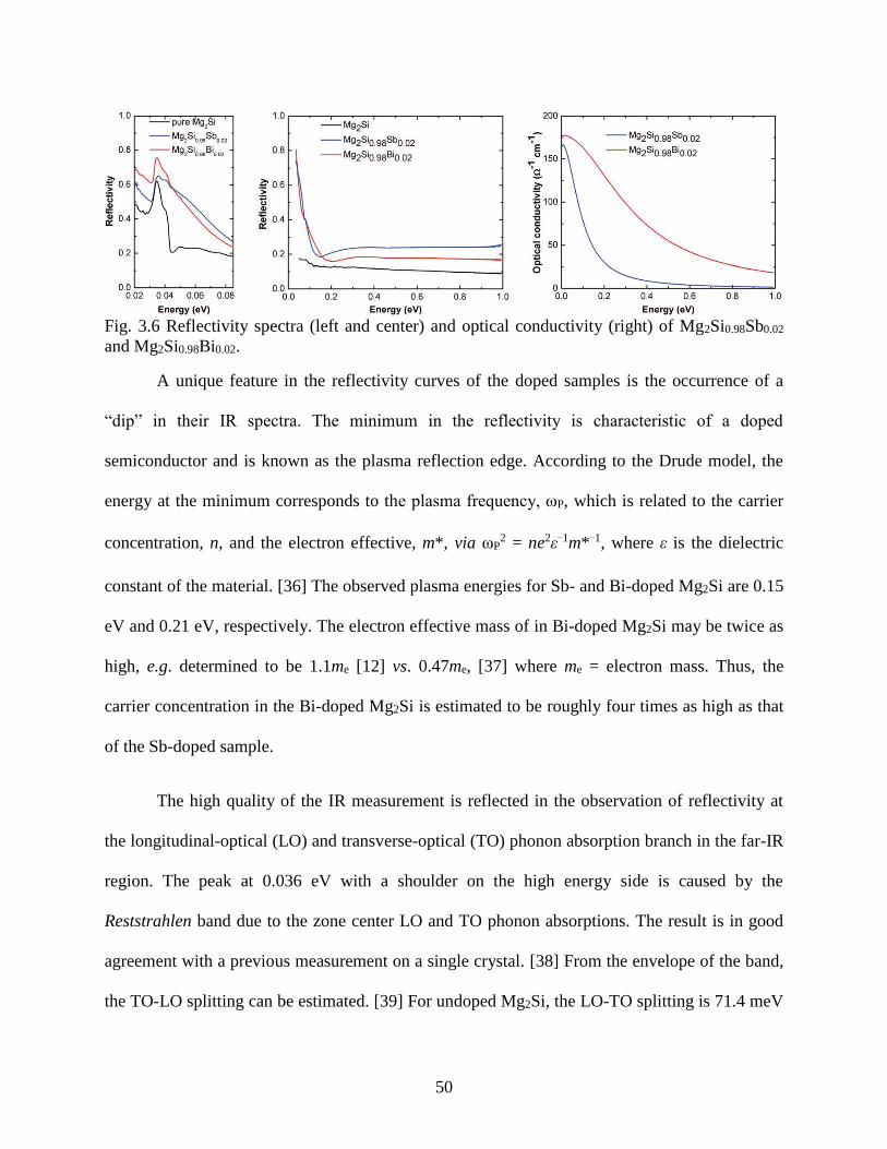
50
Fig. 3.6 Reflectivity spectra (left and center) and optical conductivity (right) of Mg2Si0.98Sb0.02
and Mg2Si0.98Bi0.02.
A unique feature in the reflectivity curves of the doped samples is the occurrence of a
“dip” in their IR spectra. The minimum in the reflectivity is characteristic of a doped
semiconductor and is known as the plasma reflection edge. According to the Drude model, the
energy at the minimum corresponds to the plasma frequency, ωP, which is related to the carrier
concentration, n, and the electron effective, m*, via ωP2 = ne2ε−1m*−1, where ε is the dielectric
constant of the material. [36] The observed plasma energies for Sb- and Bi-doped Mg2Si are 0.15
eV and 0.21 eV, respectively. The electron effective mass of in Bi-doped Mg2Si may be twice as
high, e.g. determined to be 1.1me [12] vs. 0.47me, [37] where me = electron mass. Thus, the
carrier concentration in the Bi-doped Mg2Si is estimated to be roughly four times as high as that
of the Sb-doped sample.
The high quality of the IR measurement is reflected in the observation of reflectivity at
the longitudinal-optical (LO) and transverse-optical (TO) phonon absorption branch in the far-IR
region. The peak at 0.036 eV with a shoulder on the high energy side is caused by the
Reststrahlen band due to the zone center LO and TO phonon absorptions. The result is in good
agreement with a previous measurement on a single crystal. [38] From the envelope of the band,
the TO-LO splitting can be estimated. [39] For undoped Mg2Si, the LO-TO splitting is 71.4 meV

51
or 58 cm−1. This is comparable to the previously measured value on a single crystal of 60 cm−1.
The Reststrahlen bands of Bi- and Sb-doped Mg2Si samples are somewhat broader, giving
splitting energies of 63 cm−1 and 67 cm−1, respectively. Furthermore, the frequency of the TO
vibration in Mg2Si0.98Bi0.02 is 8 meV (6.6 cm−1) lower than that of the pure sample.
Fig. 3.7 Carrier concentration (left) and Hall mobility and electrical conductivity (right) of
Mg2Si0.98Sb0.02 (white symbols) and Mg2Si0.98Bi0.02 (black symbols).
The carrier concentration, mobility and electrical conductivity are depicted in Fig. 3.7 for
both Mg2Si0.98Sb0.02 and Mg2Si0.98Bi0.02. Between 5 K and 300 K, no noticeable temperature
dependence of the Hall coefficient, RH, (and thus the carrier concentration) was detected, e.g. for
Bi-doped Mg2Si, RH ranged from -0.0677 cm3C−1 at 5 K to -0.0658 cm3C−1 at 300 K, the
negative sign being indicative of the expected n-type character of the carriers. The carrier
concentrations of n = 3.5 × 10¹⁹ electrons per cm3 and 9.5 × 10¹⁹ electrons per cm3 for Sb and Bi-
doped Mg2Si, respectively, are in qualitative agreement with our TEM and electronic structure
studies: replacing Si with Pn = Sb or Bi increases the valence electron count, but not all Pn atoms
replaced Si, as we found Mg3Pn2 in the grain boundaries. Nominally, replacing 2% of Si with Pn
would result in an extrinsic charge carrier concentration of n = 3.1 × 1020 cm−3, considering that
each Pn atom comprises one more valence electron than Si. Furthermore, this is in good

52
agreement with the estimated ratio of the carrier concentration from the reflectance spectroscopy
experiments, where the Bi sample appeared to have a much higher carrier concentration.
Similarly, Nolas et al. determined n = 1.5 × 1020 cm−3 for the same Sb content, [37] and
Tani et al. found n = 1.5 × 1020 cm−3 for the same Sb [40] and n = 1.1 × 1020 cm−3 for the same Bi
concentration, [13] while Bux et al. [12] were able to use all extra electrons from Bi after ball-
milling, followed by spark-plasma-sintering, resulting in a value of n = 3.2 × 1020 cm−3 (Tables
3.1 and 3.2).
Table 3.1 Thermoelectric properties of Mg2Si0.98Sb0.02 at 300 K-320 K (first value) and at ≈800
K (second value).
Property Our work Nolas et al.37 Tani et al.40 Ioannou et al.42
σ (Ω−1cm−1) 493-217 1000 1980-650 2850-1200
-α (μVK−1) 116-229 75 90-195 62-130
κ (Wm−1K−1) 6.7 6.58-3.72 8.53-N/A
n (cm−3) 3.5 × 10¹⁹ 1.2 × 10²⁰ 1.5 × 10²⁰ 2.5 × 10²⁰
μ (cm2V−1s−1) 50 83 72
ZT 0.03 0.006-0.51 0.05-0.32
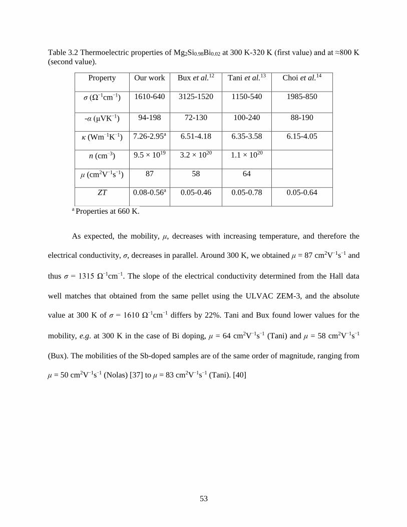
53
Table 3.2 Thermoelectric properties of Mg2Si0.98Bi0.02 at 300 K-320 K (first value) and at ≈800 K
(second value).
Property Our work Bux et al.12 Tani et al.13 Choi et al.14
σ (Ω−1cm−1) 1610-640 3125-1520 1150-540 1985-850
-α (μVK−1) 94-198 72-130 100-240 88-190
κ (Wm−1K−1) 7.26-2.95a 6.51-4.18 6.35-3.58 6.15-4.05
n (cm−3) 9.5 × 10¹⁹ 3.2 × 10²⁰ 1.1 × 10²⁰
μ (cm2V−1s−1) 87 58 64
ZT 0.08-0.56a 0.05-0.46 0.05-0.78 0.05-0.64
a Properties at 660 K.
As expected, the mobility, μ, decreases with increasing temperature, and therefore the
electrical conductivity, σ, decreases in parallel. Around 300 K, we obtained μ = 87 cm2V−1s−1 and
thus σ = 1315 Ω−1cm−1. The slope of the electrical conductivity determined from the Hall data
well matches that obtained from the same pellet using the ULVAC ZEM-3, and the absolute
value at 300 K of σ = 1610 Ω−1cm−1 differs by 22%. Tani and Bux found lower values for the
mobility, e.g. at 300 K in the case of Bi doping, μ = 64 cm2V−1s−1 (Tani) and μ = 58 cm2V−1s−1
(Bux). The mobilities of the Sb-doped samples are of the same order of magnitude, ranging from
μ = 50 cm2V−1s−1 (Nolas) [37] to μ = 83 cm2V−1s−1 (Tani). [40]

54
Fig. 3.8 compares the electrical conductivities (left) and Seebeck coefficients (right) of
Mg2Si0.98Sb0.02 and Mg2Si0.98Bi0.02 from 300 K to 840 K, measured using the ZEM-3. The
electrical conductivity of Mg2Si0.98Bi0.02 continues to decrease throughout this temperature range,
as does the σ of Mg2Si0.98Sb0.02. The latter is significantly smaller (σ = 490 Ω−1cm−1 at 300 K),
mostly because of the smaller carrier concentration by a factor of roughly 3. This difference
causes, in turn, the absolute Seebeck coefficient of the Sb-doped material to be larger, e.g. S = -
116 μVK−1 vs. -94 μVK−1 at 300 K. The calculated Seebeck coefficient was smaller, because the
calculation assumed that all extra electrons from Sb were available as charge carriers. That the
carrier concentration is the main cause for these differences is supported by the similarities of
carrier concentration, electrical conductivity, and Seebeck coefficient of Mg2Si0.98Bi0.02 with
Tani’s sample, [13] while Bux’s sample has a higher carrier concentration and electrical
conductivity, and a lower Seebeck coefficient. [12]
Fig. 3.8 Electrical conductivity (left) and Seebeck coefficient (right) of Mg2Si0.98Sb0.02 (white
symbols) and Mg2Si0.98Bi0.02 (black symbols).
From the Seebeck coefficient, one can derive the electron effective mass, if the carrier
concentration is known and assuming energy independent scattering and parabolic bands, via S =
8/3πkB2e−1h−2m*T(1/3πn−1)2/3. [41] At 300 K, this results in m* = 0.62me for the Sb case and m*

55
= 1.06me for the Bi case, in qualitative agreement with Nolas’ 0.50me for Sb and Bux’s 1.1me for
Bi. Relating this to the plasma frequencies discussed above with our experimental values for the
carrier concentration, we calculate m*(Bi)/m*(Sb) = n(Bi)ωP(Bi) − 2/{n(Bi)ωP(Bi) − 2} = 1.38,
compared to 1.06/0.62 = 1.71 from the Seebeck data.
Finally, the thermal conductivity, κ, of a second Mg2Si0.98Bi0.02 sample was determined
up to 660 K, yielding decreasing values from 7.3 W m−1K−1 at 300 K to 3.0 Wm−1K−1 at 660 K
(Fig. 3.9, left). These numbers, being significantly lower than those of undoped Mg2Si, agree
well with those of other authors working on this system (Table 3.2). Assuming these two Bi-
doped materials have the same carrier concentration, as they were prepared the same way, this
results in comparable (estimated) figure-of-merit values, e.g. ZT = 0.56 at 660 K (Fig. 3.9, right),
with the Bi sample from Tani (0.54 at 660 K), [13] which exhibited roughly the same carrier
concentration. On the other hand, the Bi-doped material from Bux et al., with its higher carrier
concentration, exhibited smaller ZT values, e.g. 0.38 at 660 K. [12]
Fig. 3.9 Thermal conductivity (left) and estimated figure of merit (right) of Mg2Si0.98Bi0.02.

56
3.4 Conclusions
We have prepared Sb- and Bi-doped Mg2Si samples via annealing, followed by hot-
pressing. Part of the dopants replace Si, as shown via STEM-HAADF, while the rest form
Mg3Sb2 and Mg3Bi2, found between the grains of doped Mg2Si particles.
DFT calculations were performed both on pure and doped Mg2Si models, resulting in the
correct band gap size after GW correction, in accordance with the results from absorbance
spectroscopy. These calculations also showed the validity of the rigid band approximation for
calculating the transport properties in dependence of the electron concentration.
As the addition of Sb and Bi only partly led to Si substitution, the experimentally
determined carrier concentration was lower than originally expected. These findings support
those of Tani et al., who used a different synthesis and consolidation method (spark-plasma-
sintering vs. hot-pressing), whereas Bux et al. obtained higher carrier concentration at the same
nominal Bi concentration after incremental ball-milling. Therefore, Bux et al. found larger
electrical conductivity and a smaller Seebeck coefficient, yet ultimately smaller ZT values at the
2% doping level.
In conclusion, the presence of Sb and Bi between the grains of doped Mg2Si may well be
advantageous with respect to the thermoelectric performance.
Acknowledgements
This work was sponsored by AUTO21 (Network Centres of Excellence) and General
Motors. The use of U2A beamline was supported by COMPRES under NSF Cooperative
Agreement EAR 11-57758 and CDAC (DE-FC03-03N00144). The National Synchrotron Light
Source, Brookhaven National Laboratory, is supported by the U.S. Department of Energy, Office
57
of Science, Office of Basic Energy Sciences under Contract No. DE-AC02- 98CH10886.
Synchrotron work at the Canadian Light Source was made possible by support from NSERC,
NRC, CIHR, and the University of Saskatchewan.
References
[1] J. Yang and F. R. Stabler, J. Electron. Mater., 2009, 38, 1245–1251.
[2] D. M. Rowe, Thermoelectrics Handbook: Macro to Nano, CRC Press, Taylor & Francis
Group, Boca Raton, FL, USA, 2006.
[3] L. E. Bell, Science, 2008, 321, 1457–1461.
[4] M. G. Kanatzidis, Chem. Mater., 2010, 22, 648–659.
[5] Y. Pei, A. LaLonde, S. Iwanaga and G. J. Snyder, Energy Environ. Sci., 2011, 4, 2085–
2089.
[6] K. Biswas, J. He, I. D. Blum, C.-I. Wu, T. P. Hogan, D. N. Seidman, V. P. Dravid and M.
G. Kanatzidis, Nature, 2012, 489, 414–418.
[7] Q. Guo, M. Chan, B. A. Kuropatwa and H. Kleinke, Chem. Mater., 2013, 25, 4097–4104.
[8] B. Wölfing, C. Kloc, J. Teubner and E. Bucher, Phys. Rev. Lett., 2001, 86, 4350–4353.
[9] E. S. Toberer, S. R. Brown, T. Ikeda, S. M. Kauzlarich and G. J. Snyder, Appl. Phys. Lett.,
2008, 93, 062110.
[10] X. Shi, J. Yang, J. R. Salvador, M. Chi, J. Y. Cho, H. Wang, S. Bai, J. Yang, W. Zhang
and L. Chen, J. Am. Chem. Soc., 2011, 133, 7837–7846.
[11] E. N. Nikitin, V. G. Bazanov and V. I. Tarasov, Sov. Phys. Solid State, 1961, 3, 2648–
2652.
[12] S. K. Bux, M. T. Yeung, E. S. Toberer, G. J. Snyder, R. B. Kaner and J.-P. Fleurial, J.
Mater. Chem., 2011, 21, 12259–12266.
[13] J.-i. Tani and H. Kido, Physica B, 2005, 364, 218–224.
[14] S.-M. Choi, K.-H. Kim, I.-H. Kim, S.-U. Kim and W.-S. Seo, Curr. Appl. Phys., 2011, 11,
S388–S391.
[15] W. Liu, X. Tan, K. Yin, H. Liu, X. Tang, J. Shi, Q. Zhang and C. Uher, Phys. Rev. Lett.,
2012, 108, 166601.

58
[16] V. K. Zaitsev, M. I. Fedorov, E. A. Gurieva, I. S. Eremin, P. P. Konstantinov, A. Y.
Samunin and M. V. Vedernikov, Phys. Rev. B: Condens. Matter, 2006, 74, 045207.
[17] X. Zhang, H. Liu, Q. Lu, J. Zhang and F. Zhang, Appl. Phys. Lett., 2013, 103, 063901.
[18] E. J. Kirkland, Image Simulation in Transmission Electron Microscopy, Cornell
University, Ithaca, NY, USA, 2006, pp. 1–14.
[19] J. P. Perdew, K. Burke and M. Ernzerhof, Phys. Rev. Lett., 1996, 77, 3865–3868.
[20] G. Kresse and J. Hafner, Phys. Rev. B: Condens. Matter, 1993, 47, 558–561.
[21] G. Kresse and J. Hafner, Phys. Rev. B: Condens. Matter, 1994, 49, 14251–14269.
[22] G. Kresse and J. Furthmüller, Comput. Mater. Sci., 1996, 6, 15–50.
[23] G. Kresse and J. Furthmüller, Phys. Rev. B: Condens. Matter, 1996, 54, 11169–11186.
[24] L. Hedin, Phys. Rev., 1965, 139, A796–A823.
[25] P. García-González and R. W. Godby, Phys. Rev. B: Condens. Matter, 2001, 63, 075112.
[26] P. E. Blöchl, Phys. Rev. B: Condens. Matter, 1994, 50, 17953– 17979.
[27] G. Kresse, Phys. Rev. B: Condens. Matter, 1999, 59, 1758– 1775.
[28] M. Chen, in First-principles Modeling of Thermoelectric Materials, PhD thesis,
Theoretical Solid State Chemistry, Vienna University of Technology, Vienna, Austria,
2012.
[29] G. K. H. Madsen and D. J. Singh, Comput. Phys. Commun., 2006, 175, 67–71.
[30] A. B. Kuzmenko, Rev. Sci. Instrum., 2005, 76, 083108.
[31] A. Stella, A. D. Brothers, R. H. Hopkins and D. W. Lynch, Phys. Status Solidi, 1967, 23,
697–702.
[32] P. Boulet and M.-C. Record, J. Chem. Phys., 2011, 135, 234702.
[33] F. Tran and P. Blaha, Phys. Rev. Lett., 2009, 102, 226401.
[34] J. J. Pulikkotil, D. J. Singh, S. Auluck, M. Saravanan, D. K. Misra, A. Dhar and R. C.
Budhani, Phys. Rev. B: Condens. Matter, 2012, 86, 155204.
[35] B. Arnaud and M. Alouani, Phys. Rev. B: Condens. Matter, 2001, 64, 033202.
59
[36] M. Fox, Optical Properties of Solids, Oxford University Press, New York City, NY, USA,
2010.
[37] G. S. Nolas, D. Wang and M. Beekman, Phys. Rev. B: Condens. Matter, 2007, 76, 235204.
[38] D. McWilliam and D. W. Lynch, Phys. Rev., 1963, 130, 2248–2252.
[39] P. Y. Yu and M. Cardona, Fundamentals of Semiconductors: Physics and Materials
Properties, Springer, New York, NY, USA, 1998.
[40] J.-i. Tani and H. Kido, Intermetallics, 2007, 15, 1202– 1207.
[41] M. Cutler, J. F. Leavy and R. L. Fitzpatrick, Phys. Rev., 1964, 133, A1143–A1152.
[42] M. Ioannou, G. Polymeris, E. Hatzikraniotis, A. U. Khan, K. M. Paraskevopoulos and T.
Kyratsi, J. Electron. Mater., 2013, 42, 1827–1834.
60
CHAPTER 4
LOCAL STRUCTURE AND THERMOELECTRIC PROPERTIES OF Mg2Si0.977-
xGexBi0.023 (0.1 ≤ x ≤ 0.4)
In Chapter 3, we demonstrate that enhancement of the thermoelectric performance can be
achieved by adding single dopant Sb or Bi to the Mg2Si with a best ZT of about 0.6 at 700 K for
Mg2Si0.98Bi0.02. A recent report shows Sb and Bi are promising dopants in the Mg2Si1-x(Ge,Sn)x
system reaching ZT values of 1.2 and 1.4 at 823 K respectively [21]. More recently, Kim et al.
published a study of the Mg2Si0.7Ge0.3 system with different Bi concentrations. It was shown that
through doping with heavier Bi the thermal conductivity was lowered to 2.2 Wm−1K−1 in
Mg2Si0.7Ge0.3Bi0.02 at 823 K; consequently, a maximum ZT of 0.79 was obtained. [22].
For this chapter, we investigated the thermoelectric properties of multiple-doped Mg2Si.
For this purpose, we replaced Si by Ge in Bi-doped Mg2Si to study the effects on the local
structure, electrical transport and thermoelectric properties at different Ge concentrations. To
understand the role of Ge, the concentration of Bi was fixed at the optimum ZT value of
Mg2Si0.977-xGexBi0.023 (0.1 ≤ x ≤ 0.4). In this way, the effects of Ge contents on the band structure
and thermoelectric properties could be systematically studied by experimental and theoretical
methods. Once again, dc conductivities of the doped samples were extracted from the analysis of
infrared reflectivity spectra employing the Drude free-electron model. As shown in the previous
chapter, we found the dc conductivity determined by infrared measurements was lower than that
obtained from in-situ four probe measurements on the bulk sample. We attributed the
discrepancy to the consequence of non-uniform distribution of the dopants in the samples. In
addition, we extracted the electron effective masses of the samples. To augment the
interpretation of the experimental results, electronic structures of the doped samples were
computed using density functional theory (DFT). The slopes of electronic densities of states
61
(DOS) at the Fermi level of the Ge- and Bi-doped Mg2Si samples were found to be similar. The
results indicate that both Ge- and Bi-doped samples should have had comparable Seebeck
coefficients. Finally, experimentally it was found that Mg2Si0.677Ge0.3Bi0.023 at 300 K has a
thermal conductivity of 2.7 Wm-1K-1, which is slightly lower than that of the pure Mg2Si: 7 Wm-
1K-1. A performance figure of merit ZT of 0.65 was achieved at 700 K in the
Mg2Si0.677Ge0.3Bi0.023 sample. This is about 8% higher than the single-doped sample at 700 K.
The results of this study have been published in
N. Farahi, S. Prabhudev, G. A. Botton, J. Zhao, J. S. Tse, Z. Liu, J. R. Salvador, and H.
Kleinke, “Local structure and thermoelectric properties of Mg2Si0.977-xGexBi0.023 (0.1 ≤ x ≤ 0.4),”
Journal of Alloys and Compounds, vol. 644, pp. 249-255, 2015.
The authors’ contributions are as follow:
N. Farahi and H. Kleinke synthesized the samples and performed the thermoelectric
property measurements.
J. Zhao and J. S. Tse collected infrared transmission and reflectivity spectrum, performed
the analysis to extract the dielectric function and transport properties, and calculated the
electronic structures.
S. Prabhudev and G. A. Botton performed the STEM measurement.
J. R. Salvador performed the Hall measurement.
Z. Liu assisted in performing infrared experiments at BNL.
All authors contributed to the writing and editing of the manuscript.

62
Abstract
We investigated the effect of germanium substitution for silicon in bismuth doped Mg2Si.
This alloying reduces the thermal conductivity from above 7 Wm-1K-1 to 2.7 Wm-1K-1 at around
300 K in part due to the added mass contrast. High resolution transmission electron microscopy
(HRTEM) revealed the presence of Ge-rich domains within the Mg2(Si,Ge,Bi) particles,
contributing to decreasing thermal conductivity with increasing Ge content up to 0.3 Ge per
formula unit. The electrical conductivity also decreases with Ge alloying because of the
increasing amount of scattering centers, while the Seebeck coefficient increased only very
slightly. In total, the positive effect of Ge substitution on the thermoelectric properties of Bi
doped Mg2Si resulted in a figure of merit of 0.7 at 773 K for Mg2Si0.677Ge0.3Bi0.023 sample. The
optimum amount of Bi seems to be 0.023 per formula unit (0.77 at%), since lower Bi content
resulted in electrical conductivity that is too low, and higher Bi content generated the Mg3Bi2
intermetallic phase.
4.1 Introduction
Undoubtedly, energy is one of the biggest challenges that mankind faces in this era. With
simultaneous reduction of fossil fuel resources and increase in population around the world,
reliance on consuming fossil fuels would not be feasible without proper energy management.
Different strategies are being pursued to reduce the dependency on fossil fuels, through the
development of a variety of alternative and renewable energy sources. To convert waste heat into
useful energy, thermoelectric (TE) materials are inimitable due to their unique ability to convert
heat into electricity. As one of the emerging technologies, certain obstacles such as efficiency,
profusion and toxicity of these materials need to be addressed before establishing them for
industrial applications.

63
The criteria for evaluating the efficiency of a thermoelectric material is its figure of merit
ZT, which is expressed as ZT = TS2σκ-1. S, σ, κ and T represent the Seebeck coefficient, electrical
conductivity, thermal conductivity and absolute temperature, respectively. Many of the current
state-of-the-art thermoelectric materials are based on toxic elements such as lead [1,2] and
thallium [3], or on rare elements such as ytterbium [4] or tellurium [5]. To be applicable to large
scale industrial production, new, highly efficient, TE materials should be comprised of low cost,
non-toxic and abundant elements. To that end, magnesium silicide has attracted enormous
attention as a potential, next generation, high efficiency TE material, especially in medium
temperature range applications such as in the automotive waste heat recovery [6].
One of the main features of materials with high ZT is their low thermal conductivity,
which can be achieved through phonon engineering [7], resonant bonding [8], lone pair electrons
[9], solid solutions [10], and by introducing more grain boundary interfaces via nano-structuring
[11-13]. Magnesium silicide shows great compositional flexibility as evidenced by its formation
of solid solutions with tin [14] or germanium [15-18] on the silicon position. Introducing these
heavy elements reduced the room temperature thermal conductivity of Mg2Si from around 10
Wm-1K-1 [19] to approximately 3 Wm-1 K-1 [18]. Although the powder patterns of compounds
with tin or germanium appear to be pure phases within the limit of the technique, microstructural
investigations performed by scanning electron microscopy reveal the existence of Ge/Sn rich
regions. This indicates that the larger elements will not completely substitute for Si, or that
reaching equilibrium compositions require prohibitively long annealing times due to sluggish
solid state diffusion processes.
To enhance the figure of merit, the electrical conductivity needs to be increased
simultaneously with κ reduction, which may be achieved through doping. So far, Sb, Fe, In, Al

64
and Au have been shown to behaved as n-type dopants for Mg2Si0.6Ge0.4, while Cu, Ag, B and
Ga were used as p-type dopants with limited success [18,20]. Sb and Bi have proven to be
promising dopants in the Mg2Si1-x(Ge,Sn)x system by enhancing ZT to 1.2 and 1.4 at 823 K,
respectively [21]. To better understand the role of Ge, the doping level of bismuth was fixed in
the present study at its optimum value, and the effects of the different Ge content on the band
structure, thermoelectric properties as well as the micro- and nano-structure of Mg2Si0.977-
xGexBi0.023 (0.1 ≤ x ≤ 0.4) were investigated. During our investigations, Kim et al. published a
study of the Mg2Si0.7Ge0.3 system with different Bi additions [22].
4.2 Experiment
Bismuth-doped Mg2Si1-xGex samples were synthesized starting from the elements in a
tantalum crucible according to the nominal stoichiometric ratio in an argon-filled glove box. We
used Mg chips (99.98%, Sigma Aldrich, 4-30 mesh), Si powder (99.9%, Alfa Aesar, -100 mesh),
Ge pieces (99.9999+%, Alfa Aesar, ≤2 cm) and Bi granules (99.99%, Sigma Aldrich). The
tantalum crucibles were sealed under argon with an arc melter, and then placed into silica tubes.
After sealing under vacuum, the tubes were heated in a resistance furnace at 923 K for a week.
Then the furnaces were switched off to allow for fast cooling down to room temperature. To
obtain pure products, the samples were ground and then annealed at 1173 K for another week
and thereafter cooled down by turning off the furnace. The purity of the synthesized samples was
examined by using an Inel powder X-ray diffractometer with Cu Kα1 radiation and a position
sensitive detector (available as Fig. B.1 in the Supporting Information). All samples were pure,
except for traces of MgO as also observed by others [21,23,24]. In the end, we settled on 0.023
Bi per formula unit, because using 0.03 or more Bi resulted in the formation of Mg3Bi2, as found
in the X-ray powder diffraction patterns. Lattice parameter refinements yielded a smooth

65
increase with increasing Ge content as expected based on the Si/Ge size ratio, resulting in a =
6.3670(2) Å (0.1 Ge), 6.37011(9) Å (0.2 Ge), 6.37363(4) Å (0.3 Ge), and 6.37648(6) Å (0.4 Ge).
To be able to perform the physical property measurements on fully dense specimens, the
annealed samples were ground and then hot pressed for two hours at 973 K under 56 MPa in an
argon atmosphere using an Oxy-Gon hot press. The pressure was released after sintering to
reduce strain and stress on the pellets during cooling. The hot-pressed billets were 12.7 mm in
diameter and 3 mm thick. These preparation methods are different from those used by Kim, who
used 773 K for annealing for six hours, followed by hot-pressing for two hours at 1073 K under
70 MPa [22], i.e. using a higher temperature and pressure in the last step.
To determine the thermal conductivity (κ) of the pressed samples, thermal diffusivity (α)
measurements were carried out under flowing Ar by using Anter Flashline FL3000 thermal
properties analyzer between 300 K and 800 K. The obtained thermal diffusivity values were then
multiplied by the density (d) of the pellets, as measured via the Archimedes method, and the
specific heat (Cp) of the compounds, as calculated from the Dulong–Petit approximation, to yield
κ = α d Cp. In order to verify the suitability of the Dulong–Petit approximation, specific heat
measurements were performed on the samples with high Ge content (Fig. B.2) using a Netzsch
404 C differential scanning calorimeter, and the measured values were in good agreement with
our approximation.
To obtain the electrical conductivity (σ) and Seebeck coefficient (S) of the samples, the
above-mentioned pellets were cut into rectangular bars with the dimensions of approximately 12
× 2 × 2 mm. The measurements were performed under a static helium atmosphere between 300
K and 800 K by using an ULVAC-RIKO ZEM-3 system.
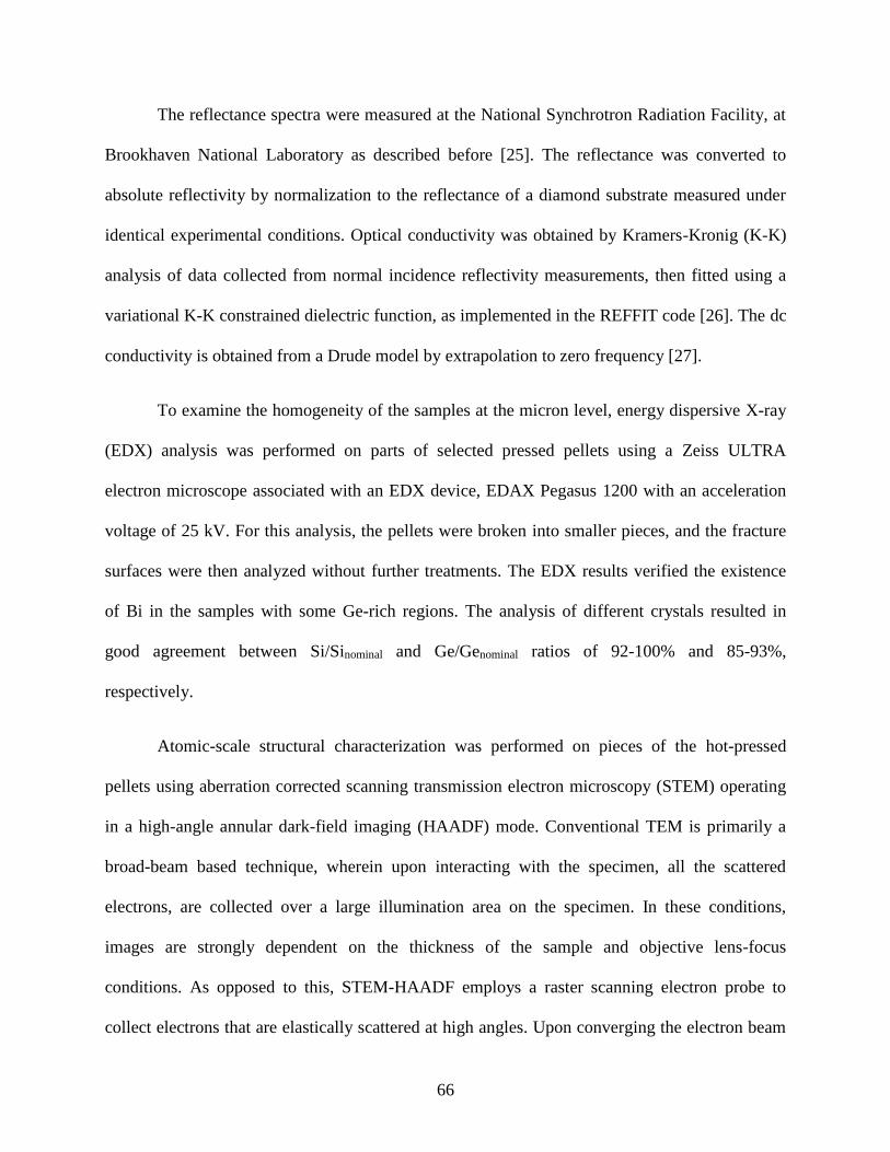
66
The reflectance spectra were measured at the National Synchrotron Radiation Facility, at
Brookhaven National Laboratory as described before [25]. The reflectance was converted to
absolute reflectivity by normalization to the reflectance of a diamond substrate measured under
identical experimental conditions. Optical conductivity was obtained by Kramers-Kronig (K-K)
analysis of data collected from normal incidence reflectivity measurements, then fitted using a
variational K-K constrained dielectric function, as implemented in the REFFIT code [26]. The dc
conductivity is obtained from a Drude model by extrapolation to zero frequency [27].
To examine the homogeneity of the samples at the micron level, energy dispersive X-ray
(EDX) analysis was performed on parts of selected pressed pellets using a Zeiss ULTRA
electron microscope associated with an EDX device, EDAX Pegasus 1200 with an acceleration
voltage of 25 kV. For this analysis, the pellets were broken into smaller pieces, and the fracture
surfaces were then analyzed without further treatments. The EDX results verified the existence
of Bi in the samples with some Ge-rich regions. The analysis of different crystals resulted in
good agreement between Si/Sinominal and Ge/Genominal ratios of 92-100% and 85-93%,
respectively.
Atomic-scale structural characterization was performed on pieces of the hot-pressed
pellets using aberration corrected scanning transmission electron microscopy (STEM) operating
in a high-angle annular dark-field imaging (HAADF) mode. Conventional TEM is primarily a
broad-beam based technique, wherein upon interacting with the specimen, all the scattered
electrons, are collected over a large illumination area on the specimen. In these conditions,
images are strongly dependent on the thickness of the sample and objective lens-focus
conditions. As opposed to this, STEM-HAADF employs a raster scanning electron probe to
collect electrons that are elastically scattered at high angles. Upon converging the electron beam
67
into a sub-angstrom probe, an atomic-scale image of materials can be obtained. The high angle
annular dark field (HAADF) detector, as the name suggests, is a detector designed in an annular
geometry and placed in a diffraction plane below the sample so as to collect electrons emerging
from the specimen at high scattering angles. Since the intensity of these high-angle scattered
electrons is directly proportional to the atomic number of scattering atoms under the electron
beam, the resulting STEM-HAADF image provides an atomic number ‘‘Z’’-contrast image with
intensities proportional to Z1.6. For instance, in the case of the Mg2Si sample alloyed with Ge (Z
= 32) and Bi (Z = 83), the atomic columns containing the Ge and Bi atoms are expected to
appear significantly brighter compared to the bulk of the matrix crystal.
Atomically-resolved STEM-HAADF images were acquired using a FEI-Titan cubed
TEM, equipped with two hexapole-design spherical aberration correctors of the probe and image
forming lenses. The microscope was operated in STEM mode at an accelerating voltage of 300
kV and the images were acquired using a Fischione Instruments HAADF detector. For STEM
characterization, the samples were thinned by mechanical polishing to 180 µm thickness, then
dimple-ground with a diamond paste to a central thickness of 20 µm and finally ion milled (using
Gatan PIPS model) to electron transparency.
Density functional theory (DFT) with the Perdew-Burke-Ernzerhof (PBE) generalized
gradient approximation (GGA) [28] as applied in the Vienna ab initio simulation package
(VASP) code was used for performing the electronic structure calculations [29-32]. For the GGA
calculation, the projector-augmented wave (PAW) [33,34] method was selected with 2p63s2 and
3s23p2 as valence electrons for the Mg and Si atoms, respectively. A 4 × 4 × 4 k-point mesh was
used for the band structure calculation. For bismuth and germanium additions, a 2 × 2 × 2
supercell was generated from the Mg2Si crystal structure, where one out of 32 Si atoms was
68
replaced with a Bi atom together with three, six, nine and twelve of 32 Si atoms replaced with Ge
atoms. The compositions of the different models are thus Mg64Si31-xGexBi with x = 3, 6, 9 and
12.
4.3 Results and discussion
Fig. 4.1 shows the density of states (DOS) of the Mg2Si0.969-xGexBi0.031 (0.094 ≤ x ≤
0.375) models. Because of the excess electron stemming from the Bi atoms, the conduction band
is occupied to a small degree in each case. A slight reduction of the band gap with increasing Ge
content confirms the same experimental observation of Mg2Si1-xGex in NMR studies [23]. Close
to the Fermi level, the slope of the density of states of all the samples is very similar, which
should result in comparable Seebeck coefficient values. The magnitude of the slope is indicative
of a light band.
Fig. 4.1 Density of states of Mg2Si0.969-xGexBi0.031 (0.094 ≤ x ≤ 0.375).
69
To better understand the nature of defects that could stem from the introduction of Ge,
high resolution transmission electron microscopy (HRTEM, operating under scanning mode)
was performed on the Mg2Si0.777Ge0.2Bi0.023 sample. Fig. 4.2a displays a low magnification
STEM (Scanning transmission electron microscopy)-HAADF (High-angle annular dark-field)
image of the polycrystalline sample. Regions with bright intensities consist of atoms with higher
atomic number (Ge: 32, Bi: 83) compared to the matrix (Mg: 14, Si: 12). The concentration of
heavy atoms is higher near the outer edges of the grains, demonstrated in Fig. 4.2b and c that
depict the areas marked red and green in Fig. 4.2a, respectively. Because of the low Bi
concentration (0.77 at%) in the sample compared to Ge (6.67 at%), it is postulated that the
majority of the segregated atoms are Ge atoms, i.e. a Ge-rich domain is present at the edge of the
Mg2(Si,Ge,Bi) grains. The strain originating from the larger size of the heavier Ge atoms can be
better accommodated along the grain boundaries, causing this concentration gradient.
Fig. 4.2d shows the STEM–HAADF image corresponding to the region marked in 4.2b.
The image had a band-pass filter applied for enhanced visibility of segregated atoms. In addition
to the Ge-rich domains, as shown by the blue lines, there are atoms, most likely Mg2+ because of
its small size, occupying interstitial sites as highlighted by the lines marked in red. Consequently,
this affects the local strain distribution at the grain boundaries.
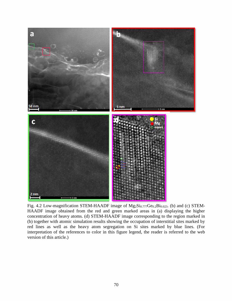
70
Fig. 4.2 Low-magnification STEM-HAADF image of Mg2Si0.777Ge0.2Bi0.023. (b) and (c) STEM-
HAADF image obtained from the red and green marked areas in (a) displaying the higher
concentration of heavy atoms. (d) STEM-HAADF image corresponding to the region marked in
(b) together with atomic simulation results showing the occupation of interstitial sites marked by
red lines as well as the heavy atom segregation on Si sites marked by blue lines. (For
interpretation of the references to color in this figure legend, the reader is referred to the web
version of this article.)
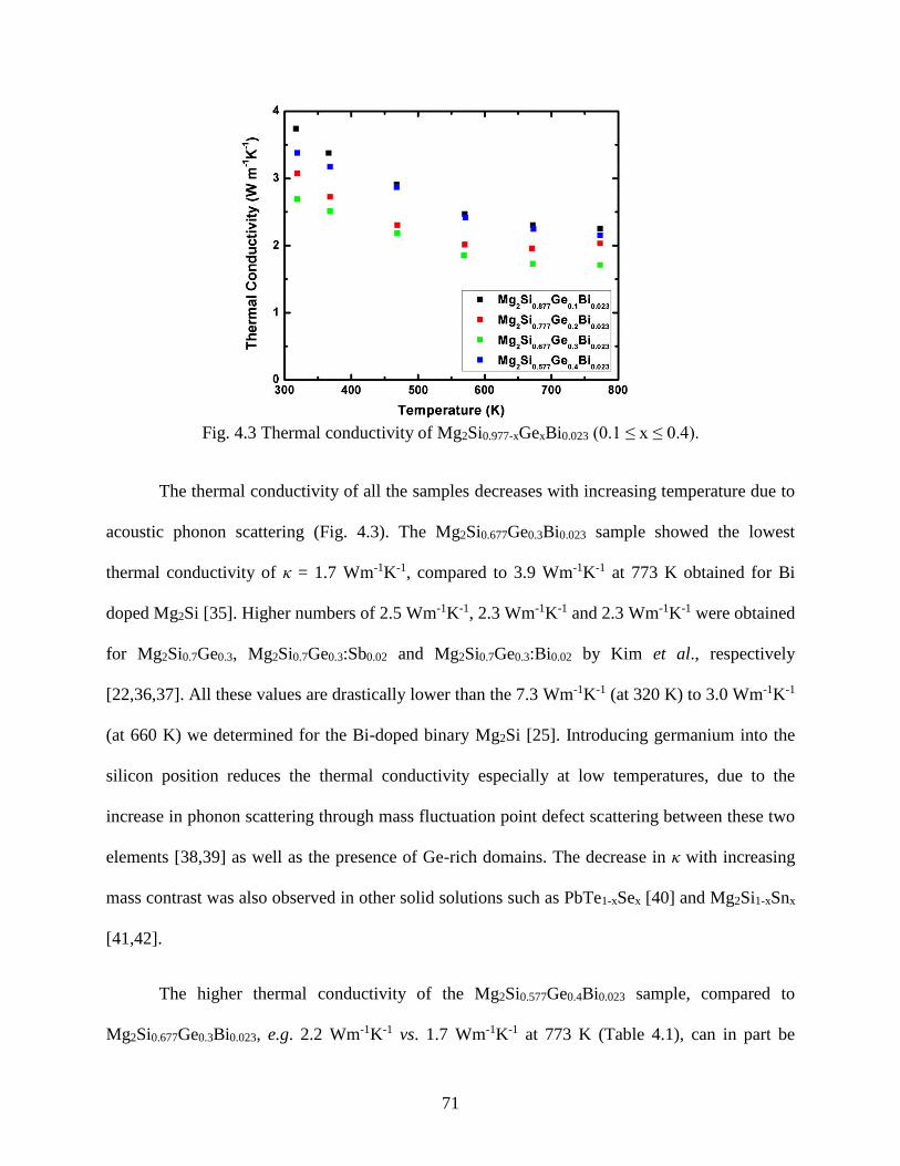
71
Fig. 4.3 Thermal conductivity of Mg2Si0.977-xGexBi0.023 (0.1 ≤ x ≤ 0.4).
The thermal conductivity of all the samples decreases with increasing temperature due to
acoustic phonon scattering (Fig. 4.3). The Mg2Si0.677Ge0.3Bi0.023 sample showed the lowest
thermal conductivity of κ = 1.7 Wm-1K-1, compared to 3.9 Wm-1K-1 at 773 K obtained for Bi
doped Mg2Si [35]. Higher numbers of 2.5 Wm-1K-1, 2.3 Wm-1K-1 and 2.3 Wm-1K-1 were obtained
for Mg2Si0.7Ge0.3, Mg2Si0.7Ge0.3:Sb0.02 and Mg2Si0.7Ge0.3:Bi0.02 by Kim et al., respectively
[22,36,37]. All these values are drastically lower than the 7.3 Wm-1K-1 (at 320 K) to 3.0 Wm-1K-1
(at 660 K) we determined for the Bi-doped binary Mg2Si [25]. Introducing germanium into the
silicon position reduces the thermal conductivity especially at low temperatures, due to the
increase in phonon scattering through mass fluctuation point defect scattering between these two
elements [38,39] as well as the presence of Ge-rich domains. The decrease in κ with increasing
mass contrast was also observed in other solid solutions such as PbTe1-xSex [40] and Mg2Si1-xSnx
[41,42].
The higher thermal conductivity of the Mg2Si0.577Ge0.4Bi0.023 sample, compared to
Mg2Si0.677Ge0.3Bi0.023, e.g. 2.2 Wm-1K-1 vs. 1.7 Wm-1K-1 at 773 K (Table 4.1), can in part be
72
explained by its higher relative density (98%, compared to 96% of the other samples), which
facilitates both phonon and electron transportation. The extent of this effect may be estimated via
the Maxwell-Eucken correction (Eq. (4.1)):
κp = κ0 1−𝑃
1+𝛽𝑃 (4.1)
Therein, κP is the measured thermal conductivity with a porosity P, and κ0 the theoretical
thermal conductivity at full density, i.e. P = 0.With porosities of 4% for the 0.3 Ge sample and 2%
for the 0.4 Ge sample and setting β = 2 for spherical pores, we calculated κ0 values of 1.9 Wm-
1K-1 and 2.3 Wm-1K-1 at 773 K, respectively. Thusly, the different density cannot explain the
large difference of 17% in κ alone; an additional explanation might be the possible existence of
small amounts of unreacted Ge in the sample with the higher Ge amount, noting that elemental
Ge has a thermal conductivity of the order of 60 Wm-1K-1 (and that each measured κ value has an
experimental error of the order of ±5%).
The lattice thermal conductivity, κL, was calculated through κL = κ - κe, where κe is the
electronic thermal conductivity, which is derived from the measured electrical conductivity, σ,
via the Wiedemann–Franz relationship κe = LσT. The Lorenz numbers L were calculated by
applying the single parabolic band and elastic carrier scattering approximation via Eq. (4.2),
𝐿 = (𝑘𝐵
𝑒)
2
{(1+𝜆)(3+𝜆)𝐹𝜆(𝜂)𝐹2+𝜆(𝜂)−(2+𝜆)2𝐹2
1+𝜆(𝜂)
(1+𝜆)2𝐹2𝜆(𝜂)
} (4.2)
where Fi(η) represents the Fermi integral of order i, the reduced Fermi energy (η) is equal to
EF/(kBT), where EF is the Fermi energy, and it can be calculated as a function of temperature
from measured values of the Seebeck coefficient using Eq. (4.3). kB is the Boltzmann constant

73
and e the electron charge. Acoustical phonon scattering (λ = 0) can be assumed as the dominant
factor limiting charge carrier mobility [43].
𝑆 =𝑘𝐵
𝑒{
(2+𝜆)𝐹1+𝜆(𝜂)
(1+𝜆)𝐹𝜆(𝜂)− 𝜂} (4.3)
Fig. 4.4 Lattice thermal conductivity of Mg2Si0.977-xGexBi0.023 (0.1 ≤ x ≤ 0.4).
The calculated Lorenz numbers range from L = 1.94 × 10⁻⁸ V2K-2 for the 0.1 Ge sample at
323 K to L = 1.62 × 10⁻⁸ V2K-2 for the 0.4 Ge sample at 773 K (a complete list of all calculated
values and their temperature dependence is available in the Supporting Information as Fig. B.3).
The calculated values for the lattice thermal conductivity are presented in Fig. 4.4, which follow
the same trends as the total thermal conductivity data. The lowest value of κL = 1.2 Wm-1K-1
occurs at 773 K for Mg2Si0.677Ge0.3Bi0.023.
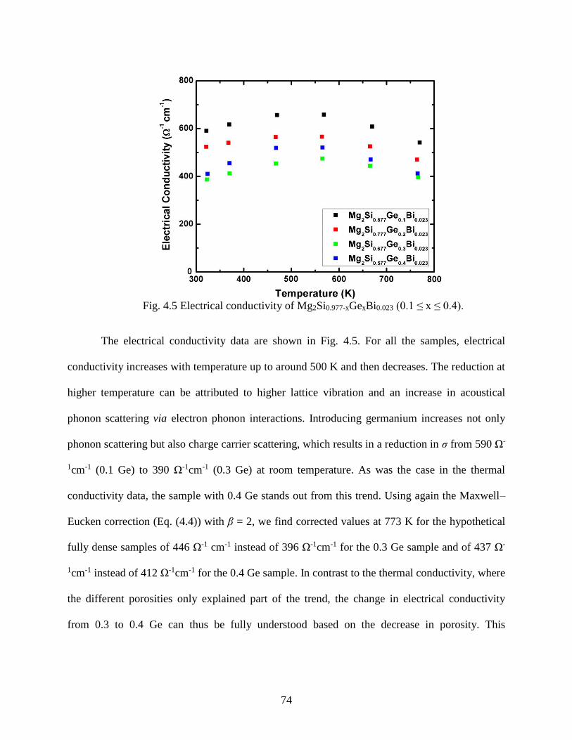
74
Fig. 4.5 Electrical conductivity of Mg2Si0.977-xGexBi0.023 (0.1 ≤ x ≤ 0.4).
The electrical conductivity data are shown in Fig. 4.5. For all the samples, electrical
conductivity increases with temperature up to around 500 K and then decreases. The reduction at
higher temperature can be attributed to higher lattice vibration and an increase in acoustical
phonon scattering via electron phonon interactions. Introducing germanium increases not only
phonon scattering but also charge carrier scattering, which results in a reduction in σ from 590 Ω-
1cm-1 (0.1 Ge) to 390 Ω-1cm-1 (0.3 Ge) at room temperature. As was the case in the thermal
conductivity data, the sample with 0.4 Ge stands out from this trend. Using again the Maxwell–
Eucken correction (Eq. (4.4)) with β = 2, we find corrected values at 773 K for the hypothetical
fully dense samples of 446 Ω-1 cm-1 instead of 396 Ω-1cm-1 for the 0.3 Ge sample and of 437 Ω-
1cm-1 instead of 412 Ω-1cm-1 for the 0.4 Ge sample. In contrast to the thermal conductivity, where
the different porosities only explained part of the trend, the change in electrical conductivity
from 0.3 to 0.4 Ge can thus be fully understood based on the decrease in porosity. This
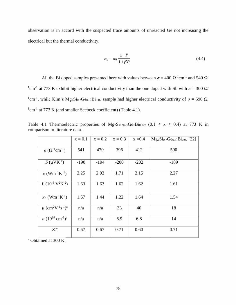
75
observation is in accord with the suspected trace amounts of unreacted Ge not increasing the
electrical but the thermal conductivity.
σp = σ0 1−𝑃
1+𝛽𝑃 (4.4)
All the Bi doped samples presented here with values between σ = 400 Ω-1cm-1 and 540 Ω-
1cm-1 at 773 K exhibit higher electrical conductivity than the one doped with Sb with σ = 300 Ω-
1cm-1, while Kim’s Mg2Si0.7Ge0.3:Bi0.02 sample had higher electrical conductivity of σ = 590 Ω-
1cm-1 at 773 K (and smaller Seebeck coefficient) (Table 4.1).
Table 4.1 Thermoelectric properties of Mg2Si0.97-xGexBi0.023 (0.1 ≤ x ≤ 0.4) at 773 K in
comparison to literature data.
x = 0.1 x = 0.2 x = 0.3 x =0.4 Mg2Si0.7Ge0.3:Bi0.02 [22]
σ (Ω−1cm−1) 541 470 396 412 590
S (µVK-1) -190 -194 -200 -202 -189
κ (Wm−1K−1) 2.25 2.03 1.71 2.15 2.27
L (10-8 V2K-2) 1.63 1.63 1.62 1.62 1.61
κL (Wm-1K-1) 1.57 1.44 1.22 1.64 1.54
µ (cm2V-1s-1)a n/a n/a 33 40 18
n (1019 cm-3)a n/a n/a 6.9 6.8 14
ZT 0.67 0.67 0.71 0.60 0.71
a Obtained at 300 K.

76
Fig. 4.6 Reflectivity spectra of Mg2Si0.977-xGexBi0.023 (x = 0.2, 0.4).
The reflectivity spectra of samples with 0.2 and 0.4 Ge are depicted in Fig. 4.6. The dc
conductivity values were calculated from the Kramers-Kronig analysis using the Drude model to
be 170 Ω-1cm-1 for the sample with 0.2 Ge and 99 Ω-1cm-1 for 0.4 Ge. These calculated values
are drastically lower than the ones measured on the pressed pellets via four point-probe
measurements, and the reason or the discrepancy is most likely due to the limited spot size
(about 400 µm2) and penetration depth of the infrared radiation. The result of these instrumental
limitations is that the signal used to extract the dc conductivity values is overly influenced by the
character of the surface states.
One of the characteristics of a doped semiconductor is the plasma reflection edge, which
is seen as a minimum in the reflectivity. Based on the Drude model, the corresponding energy at
the reflectivity minimum is related to the plasma frequency, ωP, which can be expressed as ωP2 =

77
ne2ɛ0–1ɛ-1m*-1, where n, m*, ɛ0 and ɛ are carrier concentration, electron effective mass, vacuum
permittivity and dielectric constant of the material, respectively [27]. We obtained a plasma
frequency of 1460 cm-1 for 0.2 Ge sample, and 1165 cm-1 for 0.4 Ge, corresponding to energies
of 0.18 eV and 0.14 eV, respectively. Earlier we reported 0.21 eV for Mg2Si0.98Bi0.02 [25]. The
different values for the two Ge samples are likely caused by a different effect mass (thus
mobility), as the nominal dopant concentrations are equivalent. Higher frequency/energy
correlates with lower effective mass, thus higher mobility, in accord with the higher room
temperature conductivity of the 0.2 Ge sample as compared to 0.4 Ge.
To gain more understanding of the transport properties, Hall measurements were carried
out on the samples with high Ge content (0.3 and 0.4 Ge per formula unit). The carrier
concentrations (n) of both samples are nearly the same, n ~ 7 × 10¹⁹ per cm3, consistent with
them both having the same doping level, and are both nearly temperature independent (Fig. 4.7).
Interestingly, these concentrations are significantly lower than the one determined by Kim et al.
on Mg2Si0.7Ge0.3:Bi0.02 (1.4 × 1020 cm-3), which is also consistent with their higher electrical
conductivity and lower Seebeck coefficient [22]. The different carrier concentration may be a
consequence of the lower temperature and pressure used in the consolidation process, which
might have resulted in less efficient Bi doping. For example, 0.023 Bi per formula unit would
hypothetically add 3.6 × 10²⁰ electrons per cm3, while we found only 6.9 × 1019 cm-3, compared
to Kim’s 1.4 × 1020 cm-3. On the other hand, Kim’s Sb-doped sample exhibited an unexplained
high carrier concentration of 22 × 1020 cm-3, i.e. 6 times higher than expected based on the
nominal composition.

78
Fig. 4.7 Carrier concentration of Mg2Si0.977-xGexBi0.023 (x = 0.3, 0.4).
Fig. 4.8 Hall mobility of Mg2Si0.977-xGexBi0.023 (x = 0.3, 0.4).

79
Fig. 4.8 shows an increase in the mobility (µ) of both samples with temperature. This
temperature dependence of the mobility was also observed in Sb-doped Mg2Si, where this effect
was attributed to an activated process, which originated from the presence of MgO at the grain
boundaries [44]. The increasing mobility at constant carrier concentration (as measured up to 300
K) causes the electrical conductivity to increase up to about 500 K. The slightly higher mobility
of the sample containing 0.4 Ge per formula unit, e.g. µ = 40 cm2V-1s-1 vs. 33 cm2V-1s-1 for 0.3
Ge at 300 K, is most likely a consequence of the higher relative density as above-mentioned.
Kim’s Mg2Si0.7Ge0.3:Bi0.02 exhibited only µ = 18 cm2V-1s-1 [22], likely caused by the higher
carrier concentration.
The Seebeck coefficient as a function of temperature for all the samples is shown in Fig.
4.9. Replacing one Si atom with one Bi will add one electron per atom to the system, which
results in a negative Seebeck coefficient. The room temperature Seebeck coefficient is around S
= -100 µVK-1 for all the Bi-doped samples investigated here, in accord with the similar slope of
the DOS around the Fermi level, and similar carrier concentration for at least the 0.3 Ge and 0.4
Ge samples. The S increases with temperature reaching a maximum value of -200 µVK-1 at 773
K behavior typical for a degenerate semiconductor.
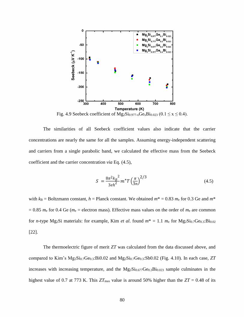
80
Fig. 4.9 Seebeck coefficient of Mg2Si0.977-xGexBi0.023 (0.1 ≤ x ≤ 0.4).
The similarities of all Seebeck coefficient values also indicate that the carrier
concentrations are nearly the same for all the samples. Assuming energy-independent scattering
and carriers from a single parabolic band, we calculated the effective mass from the Seebeck
coefficient and the carrier concentration via Eq. (4.5),
𝑆 =8𝜋2𝑘𝐵
2
3𝑒ℎ2 𝑚∗𝑇 (
𝜋3𝑛
)2/3
(4.5)
with kB = Boltzmann constant, h = Planck constant. We obtained m* = 0.83 me for 0.3 Ge and m*
= 0.85 me for 0.4 Ge (me = electron mass). Effective mass values on the order of me are common
for n-type Mg2Si materials: for example, Kim et al. found m* = 1.1 me for Mg2Si0.7Ge0.3:Bi0.02
[22].
The thermoelectric figure of merit ZT was calculated from the data discussed above, and
compared to Kim’s Mg2Si0.7Ge0.3:Bi0.02 and Mg2Si0.7Ge0.3:Sb0.02 (Fig. 4.10). In each case, ZT
increases with increasing temperature, and the Mg2Si0.677Ge0.3Bi0.023 sample culminates in the
highest value of 0.7 at 773 K. This ZTmax value is around 50% higher than the ZT = 0.48 of its
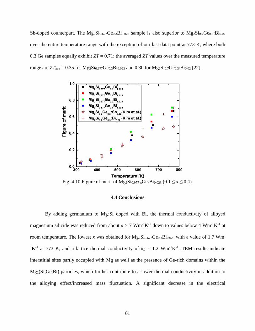
81
Sb-doped counterpart. The Mg2Si0.677Ge0.3Bi0.023 sample is also superior to Mg2Si0.7Ge0.3:Bi0.02
over the entire temperature range with the exception of our last data point at 773 K, where both
0.3 Ge samples equally exhibit ZT = 0.71: the averaged ZT values over the measured temperature
range are ZTave = 0.35 for Mg2Si0.677Ge0.3Bi0.023 and 0.30 for Mg2Si0.7Ge0.3:Bi0.02 [22].
Fig. 4.10 Figure of merit of Mg2Si0.977-xGexBi0.023 (0.1 ≤ x ≤ 0.4).
4.4 Conclusions
By adding germanium to Mg2Si doped with Bi, the thermal conductivity of alloyed
magnesium silicide was reduced from about κ > 7 Wm-1K-1 down to values below 4 Wm-1K-1 at
room temperature. The lowest κ was obtained for Mg2Si0.677Ge0.3Bi0.023 with a value of 1.7 Wm-
1K-1 at 773 K, and a lattice thermal conductivity of κL = 1.2 Wm-1K-1. TEM results indicate
interstitial sites partly occupied with Mg as well as the presence of Ge-rich domains within the
Mg2(Si,Ge,Bi) particles, which further contribute to a lower thermal conductivity in addition to
the alloying effect/increased mass fluctuation. A significant decrease in the electrical
82
conductivity also occurred with increasing Ge content, but the net effect to the thermoelectric
figure of merit is positive.
All in all, bismuth appears to be a more effective dopant than antimony in this system,
reflected in a significant enhancement (~48% higher) of thermoelectric figure of merit ZT at 773
K, compared to Kim’s Sb-doped sample. The same trend exists between Kim’s Bi- and Sb-doped
samples, which were both prepared by the same methods (though different than ours, as above-
mentioned).
Further optimization can be performed on this system by changing the doping level, the
pressing conditions, adding tin and studying the effect of nano-structuring, e.g. via ball milling or
forming composites.
Acknowledgements
The authors thankfully acknowledge AUTO21 (Network Centres of Excellence) and
General Motors for financial support of this work. JST and JZ wish to thank Westgrid for
providing the computing facilities and NSLS-I, Brookhaven National Laboratory, for
synchrotron beamtime.
References
[1] Y. Pei, J. Lensch-Falk, E. S. Toberer, D. L. Medlin, and G. J. Snyder, Adv. Funct. Mater.,
2011, 21, 241.
[2] K. Biswas, J. He, I. D. Blum, C.-I. Wu, T.P. Hogan, D. N. Seidman, V. P. Dravid, and M.
G. Kanatzidis, Nature, 2012, 489, 414.
[3] J. P. Heremans, B. Wiendlocha, and A. M. Chamoire, Energy Environ. Sci., 2012, 5, 5510.
[4] S. R. Brown, S. M. Kauzlarich, F. Gascoin, and G. J. Snyder, Chem. Mater., 2006, 18,
1873.
[5] Y. Pei, A. D. LaLonde, N. A. Heinz, and G. J. Snyder, Adv. Energy Mater., 2012, 2, 670.
83
[6] J. Yang and F. R. Stabler, J. Electron. Mater., 2009, 38, 1245.
[7] E. S. Toberer, A. Zevalkink, and G. J. Snyder, J. Mater. Chem., 2011, 21, 15843.
[8] S. Lee, K. Esfarjani, T. Luo, J. Zhou, Z. Tian, and G. Chen, Nat. Commun., 2014, 5,
3525/1.
[9] M. D. Nielsen, V. Ozolins, and J. P. Heremans, Energy Environ. Sci., 2013, 6, 570.
[10] P. F. P. Poudeu, J. D’Angelo, H. Kong, A. Downey, J. L. Short, R. Pcionek, T. P. Hogan,
C. Uher, and M. G. Kanatzidis, J. Am. Chem. Soc., 2006, 128, 14347.
[11] D. L. Medlin and G. J. Snyder, Curr. Opin. Colloid Interface Sci., 2009, 14, 226.
[12] A. J. Minnich, M. S. Dresselhaus, Z. F. Ren, and G. Chen, Energy Environ. Sci., 2009, 2,
466.
[13] W. Liu, Z. Ren, G. Chen, in: K. Koumoto, T. Mori (Eds.), Thermoelectr. Nanomater.,
Springer-Verlag, Berlin, Heidelberg, 2013, pp. 255–285.
[14] V. K. Zaitsev, Thermoelectr. Handb., CRC Press, 2005, pp. 12–29.
[15] R. J. LaBotz, D. R. Mason, and D. F. O’Kane, J. Electrochem. Soc., 1963, 110, 127.
[16] M. I. Fedorov, V. K. Zaitsev, G. N. Isachenko, I. S. Eremin, E. A. Gurieva, A. T. Burkov,
P. P. Konstantinov, and A .A. Shabaldin, in: ICT 2005. 24th Int. Conf. Thermoelectr.
2005., IEEE, 2005, pp. 110–113.
[17] Y. Noda, H. Kon, Y. Furukawa, I. A. Nishida, and K. Masumoto, Mater. Trans., 1992,
JIM 33, 851.
[18] Y. Noda, H. Kon, Y. Furukawa, N. Otsuka, I.A. Nishida, K. Masumoto, Mater. Trans.,
1992, JIM 33, 845.
[19] D. Cederkrantz, N. Farahi, K. A. Borup, B. B. Iversen, M. Nygren, and A. E. C. Palmqvist,
J. Appl. Phys., 2012, 111, 023701.
[20] H. Ihou-Mouko, C. Mercier, J. Tobola, G. Pont, and H. Scherrer, J. Alloys Comp., 2011,
509, 6503.
[21] A. U. Khan, N. Vlachos, and T. Kyratsi, Scr. Mater., 2013, 69, 606.
[22] S.-W. You, D.-K. Shin, and I.-H. Kim, J. Korean Phys. Soc., 2014, 65, 57.
[23] E. Ratai, M. P. Augustine, and S. M. Kauzlarich, J. Phys. Chem. B, 2003, 107, 12573.

84
[24] T. Ikeda, L. Haviez, Y. Li, and G. J. Snyder, Small, 2012, 8, 2350.
[25] N. Farahi, M. VanZant, J. Zhao, J. S. Tse, S. Prabhudev, G. Botton, J. R. Salvador, F.
Borondics, Z. Liu, and H. Kleinke, Dalt. Trans., 2014, 43,14983.
[26] A. B. Kuzmenko, Rev. Sci. Instrum., 2005, 76, 083108/1.
[27] M. Fox, Optical Properties of Solids, second ed., Oxford University Press, New York City,
NY, USA, 2010.
[28] J. P. Perdew, K. Burke, and M. Ernzerhof, Phys. Rev. Lett., 1996, 77, 3865.
[29] G. Kresse, Phys. Rev. B, 1996, 54, 11169.
[30] G. Kresse and J. Hafner, Phys. Rev. B, 1994, 49, 14251.
[31] G. Kresse and J. Hafner, Phys. Rev. B, 1993, 47, 558.
[32] G. Kresse and J. Furthmüller, Comput. Mater. Sci., 1996, 6, 15.
[33] P.E. Blöchl, Phys. Rev. B, 1994, 50, 17953.
[34] G. Kresse, Phys. Rev. B, 1999, 59, 1758.
[35] J. Tani and H. Kido, Phys. B Condens. Matter., 2005, 364, 218.
[36] S.-W. You and I.-H. Kim, J. Korean Phys. Soc., 2014, 64, 690.
[37] S.-W. You, D.-K. Shin, and I.-H. Kim, J. Korean Phys. Soc., 2014, 64, 1346.
[38] T. M. Tritt, Thermal Conductivity, Springer, New York City, NY, 2004.
[39] C. Kittel, Introduction to Solid State Physics, seventh ed., John Wiley & Sons Inc, New
York City, NY, 1996.
[40] H. Wang, A. D. LaLonde, Y. Pei, and G. J. Snyder, Adv. Funct. Mater., 2013, 23, 1586.
[41] M. I. Fedorov, D. A. Pshenay-Severin, V. K. Zaitsev, S. Sano, and M. V. Vedernikov, in:
Proc. ICT’03. 22nd Int. Conf. Thermoelectr. (IEEE Cat. No.03TH8726), IEEE, 2003, pp.
142–145.
[42] A. Y. Samunin, V. K. Zaitsev, P. P. Konstantinov, M. I. Fedorov, G. N. Isachenko, A. T.
Burkov, S. V. Novikov, and E. A. Gurieva, J. Electron. Mater., 2012, 42, 1676.
[43] V. I. Fistul’, Heavily Doped Semiconductors, Springer New York, Boston, MA, 1995.

85
[44] J. de Boor, T. Dasgupta, H. Kolb, C. Compere, K. Kelm, and E. Mueller, Acta Mater.,
2014, 77, 68.
86
CHAPTER 5
THERMOELECTRIC AND ELECTRICAL TRANSPORT PROPERTIES OF Mg2Si
MULTI-DOPED WITH Sb, Al AND Zn
In Chapters 3 and 4, we show that Mg2Si and Mg2Si1-xGex doped with a single element
such as Sb and Bi led to favourable enhancement of the thermoelectric figure of merit. In 2010,
Isoda et al. investigated Mg2Si0.25Sn0.75 doped with Li and Ag. [12] They found that, compared to
the undoped sample, the presence of Li (20,000 ppm) and Ag (5000 ppm) increased the Seebeck
coefficients to a maximum value of 250 µVK-1 at 500 K. In comparison with the single Li-doped
Mg2Si, Sn double-doping further doubled the carrier concentration. [13] Sb-doped Mg2Si0.5Sn0.5
compound has been synthesized with a peak power factor of 3.2× 10⁻³ Wm-1K-2 at 610 K and a
maximum ZT >0.9. This is a very promising result as the performance of this class of compound
is comparable to the current commercial PbTe-based thermoelectric materials. [14] Furthermore,
more recently Du et al. also report a maximum ZT of 0.85 obtained at 700 K for
Mg2(1+x)Si0.38Sn0.6Sb0.02 (x = 0.1) and found that the carrier concentration and electrical
conductivity were significantly enhanced. [15] Liu et al. also obtained high thermoelectric
performance for Mg2(1+x)Si0.45Sn0.537Sb0.013 (x = 0.04-0.12) with a best ZT value of 1.0 at 725 K
for x = 0.08 and a carrier concentration of 1.9-1020 cm-3. [16] Khan et al. report that an even
higher figure of merit of 1.4 can be obtained at 800 K for Mg2Si0.55Sn0.4Ge0.05 doped with Bi.
[17] le-Quoc reports Hall-effect measurements at room temperature on a thin film of Sb doped
Mg2Si1-xSnx (x = 0.4, 0.5, 0.6) and shows the Sb acted as an electron donor but the carrier
concentration increased non-linearly with the Sb content. The electrical conductivity of the Sb-
doped films, however, was still low with a charge carrier concentration less than 1019 electron-
cm-3. [18] A significant enhancement of the thermoelectric figure of merit of Mg2Si to 0.7 at 873
K was achieved more recently by double-doping the sample with a combination of Bi, Pb, and

87
Sb. It was observed that the addition of any two of the doping elements could increase the
electrical conductivity because of the increased free electrons from the dopants in the conduction
band. [19] For example, Jiang et al. found the thermoelectric performance was improved by
introducing three types of defects: Sb dopants, Mg vacancies, and Mg interstitials into
Mg2Si0.4Sn0.6-xSbx samples. [20] Isoda et al. found the highest ZT value of 0.94 for the Al/Sb
double-doped Mg2Si0.75Sn0.25 at 850 K. Therefore, Sb is considered to be an effective dopant to
increase the carrier concentration. [21]
For this chapter, the thermoelectric and electrical transport properties of Mg2Si were
investigated by multi-element-doping with Sb, Al and Zn. The compounds we studied were
Mg1.99Al0.005Zn0.005Si0.995Sb0.005 (Mg2Si:Sb0.5%Al0.5%Zn0.5%), Mg1.99Al0.01Si0.995Sb0.005
(Mg2Si:Sb0.5%Al1.0%), Mg1.995Zn0.005Si0.995Sb0.005 (Mg2Si:Sb0.5%Zn0.5%), and
Mg1.99Zn0.01Si0.995Sb0.005 (Mg2Si:Sb0.5%Zn1.0%). Once again, the electrical transport properties
of the samples were studied by mid-infrared (IR) reflectivity measurements. In addition, the
electrical resistivity and Hall coefficients were also measured by the conventional quasi-four-
probe method. Combining IR reflectivity data and independently measured Hall coefficients, the
static (dc) conductivities, effective masses and carrier concentrations of the samples studied were
determined. Our experimental collaborators also measured the temperature dependence of the
Seebeck coefficient (S), electrical conductivity (σ), and thermal conductivity (κ). From the
results, the figure of merit (ZT) and power factor (S2σ× T) of Sb, Al, and Zn multi-doped Mg2Si
samples were calculated. At 700 K, the ZT was found to be 0.7 in Mg2Si:Sb0.5%Zn0.5% and
Mg2Si:Sb0.5%Zn1.0%. This value is approximately 17% higher than single-doped Mg2Si. A
maximum ZT of 0.964 was found for Mg2Si:Sb0.5%Zn0.5% at 880 K. This value is also
comparable to the PbTe-based thermoelectrics.
88
The results of this investigation were published in
J. Zhao, Z. Liu, J. Reid, K. Takarabe, T. Iida, B. Wang, U. Yoshiya, and J. S. Tse,
“Thermoelectric properties and electrical transport properties of multi-doped Mg2Si with Sb Al
and Zn,” Journal of Materials Chemistry A, vol. 3, pp. 19774-19782, 2015.
The authors’ contributions are as follow:
J. Zhao and J. S. Tse performed powder X-ray diffraction and mid-infrared reflectivity
experiments, and performed the analysis of all the experimental data.
Z. Liu assisted in performing mid-infrared reflectivity experiments at BNL.
J. Reid assisted in performing powder X-ray diffraction experiments at CLS.
K. Takarabe, T. Iida, B. Wang, and U. Yoshiya provided the samples, and performed the
thermoelectric properties measurements in Japan.
All authors contributed to the writing and editing of the manuscript.
Abstract
Enhanced thermoelectric and electrical transport properties of Mg2Si-based
thermoelectric materials have been achieved by multi-doping with Sb, Al and Zn. Results on the
investigation of the electrical transport and thermoelectric properties of multi-doped samples
prepared using the spark plasma sintering technique are reported. Synchrotron radiation powder
X-ray diffraction was used to characterize the structures of the doped samples. The electrical
transport properties were determined from mid-infrared reflectivities, Hall effect and
conventional quasi-four probe conductivity measurements. Using the electron concentrations (N)
determined from the Hall coefficients, the effective masses (m*) were calculated from the
89
frequency of the plasma edge (ωP) of the infrared reflectivities. The thermoelectric performance
and thermoelectric figure of merits (ZT) in the temperature range of 300 K to 900 K of the doped
Mg2Si compounds were calculated from the measured temperature dependent electrical
conductivity (σ), Seebeck coefficient (S), and thermal conductivity (κ). A maximum ZT of 0.964
was found for Sb0.5%Zn0.5% doped Mg2Si at 880 K. This value is comparable to those of PbTe
based thermoelectric materials.
5.1 Introduction
Doped magnesium silicide (Mg2Si)-based alloys have been suggested to be a new
generation of high performance and environmentally friendly thermoelectric materials. [1-4]
Compared to lead-based thermoelectric materials, Mg2Si-based alloys have the merits of non-
toxicity, sustainability and low production cost. The efficiency of thermoelectric materials can be
enhanced through p- or n-type doping. [5-9] Dopants can increase the carrier concentration and
mobility of the conduction electrons. Doping with heavy atoms can also affect the lattice
vibrations and help to lower the thermal conductivity. It was reported that in the presence of Sb
and Bi, Mg2Si had exhibited good thermoelectric performance. [10] For example, Akasaka et al.
had found that the figure of merit for Bi-doped and Ag-doped, n- and p-doping, respectively, was
0.65 at 840 K and 0.1 at 566 K. [11]
More recently, p-type and n-type Mg2Si thermoelectric materials multi-doped with more
than one element have led to further enhancement of the thermoelectric figure of merit. In 2010,
Mg2Si0.25Sn0.75 doped with Li and Ag was investigated by Isoda et al. [12] Compared to the
single-doped samples, for double doped Mg2Si0.25Sn0.75 with Li (20 000 ppm) and Ag (5000
ppm) the Seebeck coefficients have increased and maximized to 250 µVK-1 at 500 K. The
previous Seebeck coefficients were found to be positive, indicating p-type doping with holes as
90
conduction carriers. In comparison with single Li-doped Mg2Si, double doping increased the
carrier concentration to more than double. [13] In 2011, the Sb doped Mg2Si0.5Sn0.5 compound
was synthesized and the peak power factor of the sample reached 3.2× 10⁻³ Wm-1K-2 at 610 K
with a maximum ZT >0.9, comparable to those of PbTe based thermoelectric materials. [14] In
addition, Du et al. reported that a maximum ZT of 0.85 was obtained at 700 K for
Mg2(1+x)Si0.38Sn0.6Sb0.02 (x = 0.1), and found that the carrier concentration and electrical
conductivity were significantly enhanced by the Mg in the interstitial sites. [15] Moreover, Liu et
al. also found high thermoelectric performance for Mg2(1+x)Si0.45Sn0.537Sb0.013 (x = 0.04-0.12)
with a maximum ZT of 1.0 at 725 K for x = 0.08 and a carrier concentration of 1.9-1020 cm-3.
[16] Khan et al. reported that an even higher figure of merit (ZT) of 1.4 can be obtained at 800 K
for the multi-doped compound of Mg2Si0.55Sn0.4Ge0.05 doped with Bi. [17] le-Quoc reported Hall
effect measurements at room temperature on a thin film of Sb doped Mg2Si1-xSnx (x = 0.4, 0.5,
0.6) and showed that Sb acted as an electron donor but the carrier concentration increased non-
linearly with the Sb content. The electrical conductivity of the Sb doped films, however, is still
low with a charge carrier concentration less than 1019 cm-3. [18] In 2014, a significant
enhancement of the thermoelectric figure of merit of Mg2Si to 0.7 at 873 K was achieved by
double-doping with a combination of Bi, Pb, and Sb. It was observed that the addition of any two
of the doping elements can increase the electrical conductivity due to the excess free electrons in
the conduction band. [19] For example, Jiang et al. found that the thermoelectric performance
was improved by introducing three types of point defects, Sb dopants, Mg vacancies, and Mg
interstitials, into Mg2Si0.4Sn0.6-xSbx samples. [20] Isoda et al. found the highest ZT value of 0.94
for the Al/Sb double-doped Mg2Si0.75Sn0.25 at 850 K. Therefore, Sb is considered to be an
effective dopant to increase the carrier concentration. [21] Previous studies have shown that

91
double or multi-doping is a promising approach to further enhance the thermoelectric figure of
merit (ZT) of Mg2Si-based thermoelectric materials.
The objective of this paper is to characterize and to better understand the effect of multi-
dopants on the host lattice of Mg2Si crystals. For this purpose, Sb, Al, and Zn multi-element-
doped Mg2Si samples were synthesized by using the spark plasma sintering technique. The
electrical transport properties were studied by mid-infrared reflectivity measurements. Since the
reflectivity is related to the dielectric function, frequency dependent optical conductivity can be
extracted from the analysis. Static (dc) conductivity is obtained by extrapolation to zero photon
energy. In addition, the electrical resistivity and Hall coefficient were also measured by the
conventional quasi-four- probe method. The thermoelectric properties of the multi-doped Mg2Si
samples were determined from the temperature dependence of the Seebeck coefficient (S),
electrical conductivity (σ), and thermal conductivity (κ). The figure of merit (ZT) and power
factor (S2σ × T) of Sb, Al, and Zn multi-doped Mg2Si samples were then calculated.
The layout of the paper is as follows. First, details on the experimental procedure will be
described. The diffraction patterns of multi-element-doped Mg2Si are compared with those of
pure Mg2Si. This is followed by a discussion on the electrical properties extracted from mid-IR
reflectivity and the conventional quasi-four probe method. Finally, the thermoelectric properties
were characterized from the results of the temperature dependence of the Seebeck coefficient (S),
electrical conductivity (σ), and thermal conductivity (κ). The figure of merit (ZT) and power
factor (S2σ × T) were calculated and discussed.
92
5.2 Experimental details
5.2.1 Synthesis and the sintering process for doped Mg2Si sample preparation
Crystal growth of polycrystalline Mg2Si was performed using an electric furnace by
lowering the temperature from slightly beyond the melting point (1378 K) of Mg2Si, and was
initiated from stoichiometric melts with Mg : Si = 2 : 1. The starting materials, Mg and Si, were
placed in an alumina crucible under argon-hydrogen forming gas (0.08 MPa). Intentional
impurities of antimony (Sb) and aluminium (Al), and an isoelectric impurity of zinc (Zn) were
incorporated in order to increase the electronic carrier concentrations and phonon scattering. The
Sb and Al dopants predominantly substitute Si and Mg, respectively, which act as donors, and Zn
is expected to show isoelectric characteristics at the Mg site, i.e., no contribution to carrier
generation but an influence over phonon behaviour, bringing about reduction in thermal
conductivity. These donor and isoelectric dopants were incorporated during the all-molten
synthesis process at 1378 K, and the resultant polycrystalline Mg2Si was pulverized to powder
with a size of 25-75 µm, then placed into a graphite die and sintered by using a plasma-activated
sintering (PAS) technique using an ELENIX Ed-PAS-III-Es. Sintering was basically performed
at 1123 K for 10 min with a pressure of 40 MPa in an Ar (0.06 MPa) atmosphere and the
sintering temperature and time were varied depending on the type of dopant that was used to
obtain a dense material. The compositions of the samples were analyzed by electron-probe
microanalysis (EPMA) using a JEOL JXA-8900. The concentration of the dopant impurities in
the samples was estimated by glow discharge mass spectrometry (GDMS) using a V.G.
Scientific VG-9000.
93
5.2.2 Powder X-ray diffraction measurements
Powder Mg2Si was purchased from Alfa Products with a purity of 99.5%. Mg2Si was
doped with nominal 0.5 at% of Sb, 0.5-1.0 at% of Al, and 0.5-1.0 at% of Zn by using the spark
plasma sintering technique. The four materials studied were Mg2Si with nominal at% of Sb0.5%
Al0.5% Zn0.5%, Sb0.5% Al1.0%, Sb0.5% Zn0.5%, and Sb0.5% Zn1.0%. Synchrotron X-ray
diffraction experiments on the pure standard and doped Mg2Si samples were performed at
CMCF-II, Canadian Light Source (CLS), using synchrotron radiation (λ = 0.68880 Å). The
diffraction patterns were analyzed using the JANA 2006 software package with the lattice
parameters determined by the Le Bail fit. [22,23]
5.2.3 Mid-infrared reflectivity measurements
Mid-infrared normal-incidence reflectance spectra of pure and Sb Zn Al multi-doped
Mg2Si samples were measured at the side-station of the U2A beamline, National Synchrotron
Radiation Facility, Brookhaven National Laboratory. Mid-infrared spectra were recorded on a
Bruker Vertex 80v FTIR spectrometer and a Hyperion 2000 IR microscope attached with a liquid
nitrogen cooled HgCdTe detector. Powder samples were prepared and placed in the 300 µm culet
of a Sintek mini type IIa diamond anvil cell. After loading the sample the DAC is closed by hand
compression to flatten the powder sample. After re-opening the DAC, one half of the flattened
sample was removed leaving half of the clean diamond face exposed. In this way, the orientation
of the sample surface and diamond support is ensured to be the same. This is critical for the
conversion of the reflectance to absolute reflectivity. The procedure is as follows: the reflectance
of the diamond phase (Id) and the sample (Isa) was measured. The reflectance of the sample was
then converted to absolute reflectivity by normalization to the reflectance of the diamond
surface. From the known reflectivity of diamond, the reflectivity of the sample-air interface (Rsa)

94
was calculated as Rsa= (Isa/Id) × (Id/I0), where Id/I0 is a constant of 0.185. All the spectral data
were collected at a resolution of 4 cm-1 and accumulated for 512 scans.
Frequency dependent optical conductivity was obtained by Kramers-Kronig (K-K)
analysis of the reflectivity data by fitting with a variational K-K constrained dielectric function,
implemented in the RefFIT code. [24,25] The frequency dependent optical conductivity was
derived from the fit to a Drude-Lorentz (DL) model and the dc conductivity obtained from
extrapolation to zero frequency.
5.2.4 Electrical transport property and thermoelectric property measurements
Polycrystalline Mg2Si fabricated by an all-molten synthesis method was used as the
source material. The Sb, Al and Zn dopants were incorporated during a melt synthesis process at
1378 K, and the resultant polycrystalline Mg2Si was pulverized to powder with a size of 25-75
µm, then placed into a graphite die and sintered by using a plasma-activated sintering (PAS)
technique using an ELENIX Ed-PAS-III-Es. Sintering was performed at a pressure of 40 MPa in
an Ar (0.06 MPa) atmosphere and the sintering temperature and time were varied depending on
the type of dopant that was used to obtain a dense material. The temperature-dependent
thermoelectric properties were measured using an ULVAC-RIKO ZEM2 to determine the
Seebeck coefficient and the electrical resistivities, and an ULVACRIKO TC-7000H to determine
the thermal conductivity over a temperature range from 300 K to 900 K. Electrical resistivity
below room temperature was measured by the standard four-probe method using a commercial
Quantum Design Physical Property Measurement System (PPMS) (1.8 K T 400 K, 0 H 70 kOe).
The Hall effect was measured at fixed temperature by changing the magnetic field strength from
-5 T to 5 T.

95
5.3 Results and discussion
High resolution synchrotron angle dispersive X-ray diffraction patterns of pure Mg2Si,
Mg2Si doped with Sb0.5%Al0.5% Zn0.5%, Sb0.5%Al1.0%, Sb0.5%Zn0.5%, and
Sb0.5%Zn1.0% were measured with a photon energy of 18 keV (λ = 0.68880 Å) on the CMCF-
II beamline, Canadian Light Source Inc. at room temperature (Fig. 5.1). The lattice constants
were determined from the full profile Le Bail fit to the diffraction patterns from 5º to 40º using
the JANA 2006 package. The X-ray diffraction pattern of pure Mg2Si can be indexed readily to
the cubic anti-fluorite (CaF2) structure with space group Fm3̅m. On increasing the diffraction
angle, the Miller indices (hkl) of the Bragg peaks are identified as (111), (200), (220), (311),
(222), (400), (331), (420), (422), (511), (440), (531) and (600) reflections. The diffraction
patterns of Mg2Si doped with Sb, Zn and Al all share the same profile as pure Mg2Si except the
Bragg peaks that have shifted noticeably to lower angles. The observation indicated that even
with a small dopant concentration (0.5-1.0%) the cubic lattice of Mg2Si is expanded. Fig. 5.2(a)
and (b) summarize the experimental lattice parameters and unit cell volumes of pure Mg2Si and
doped Mg2Si. The cubic cell parameter of pure Mg2Si a = 6.2843(9) Å is increased to 6.3506(9)
Å to 6.3634(9) Å by the addition of the dopants (Zn, Al, and Sb). This can be rationalized as the
atomic sizes of Zn and Al dopants are larger than Mg, and Sb, which replaces Si, also has a
bigger size. We can conclude unequivocally that the cubic cells of all the doped samples are
larger than pure Mg2Si. The observations also lend support to the expectation that Al and Zn
dopants will occupy the Mg sites, while Sb replaced Si in the Mg2Si crystal structure. If this is
the case, Al, Zn, and Sb doped Mg2Si are n-type semiconductors. As will be shown later, this
assignment is in agreement with the negative Hall coefficients.

96
Fig. 5.1 Angle dispersive X-ray diffraction patterns of pure Mg2Si and doped Mg2Si measured at
room temperature.

97
Fig. 5.2 (a) Lattice parameters of pure and doped Mg2Si; (b) the volume per formula of pure and
doped Mg2Si.

98
Further analysis of the lattice constants of the doped samples show, for instance, when
compared with Mg2Si:Sb0.5% Zn0.5%, that the lattice constants of Mg2Si:Sb0.5% and Zn1.0%
are expanded, possibly due to the higher doping concentration of Zn. On the other hand, between
Mg2Si:Sb0.5%Zn1.0% and Mg2Si:Sb0.5%Al1.0%, the only difference is the doped element (i.e.
Zn vs. Al). The lattice parameter in Mg2Si:Sb0.5%Zn1.0% is slightly larger, as the size of Zn is
larger than Al. In comparison, the lattice parameter of Mg2Si:Sb0.5%Zn0.5% is comparable with
Mg2Si:Sb0.5%Al0.5%Zn0.5%, suggesting that Al has a weaker effect on the expansion of the
crystal lattice, probably due to the similar atom sizes of Al and Mg atoms.
Fig. 5.3 Mid-infrared reflectivity spectra of pure and doped Mg2Si.
Infrared reflectivity experiments can provide information on the electrical transport of a
material. Mid-infrared reflectivity spectra were measured with an internal Globar radiation
source (600-8000 cm-1) installed at the U2A beamline on pure Mg2Si and Mg2Si multi-doped
with Sn Zn and Al. The electronic transport properties of the doped samples were extracted. The
experimental reflectivities of pure and multi-doped Mg2Si are compared in Fig. 5.3. The infrared
reflectivity of all the doped Mg2Si samples exhibits a Drude-like behavior at low frequency

99
indicative of doped semiconductors. In comparison, the undoped Mg2Si sample does not have
the free electron-like feature, indicating that it is a semiconductor with a small band gap. This is
to be expected as Mg2Si is a semiconductor with a small indirect band gap of 0.6 eV. [27] In
comparison to the flat and featureless reflectivity of pure Mg2Si, the reflectivities of the multi-
doped samples extrapolated to zero frequency are much higher. Note that a good conductor, such
as copper or aluminum, has a reflectivity close to unity at zero frequency.
The Sb, Zn, Al-doped Mg2Si samples show a common feature in the reflectivity curves
around 1800 cm-1. It is the appearance of a “dip” in the spectra. The minimum in the reflectivity
is the characteristic of a doped semiconductor and is known as the plasma reflection edge or
plasma dip. [28] According to the simple Drude model, the energy at the energy minimum
(plasma frequency ωP) is related to the carrier concentration (N) and the effective mass (m*), ωP2
= Ne2/ɛɛ0m* where ɛ is the dielectric constant of the material, and ɛ0 is the vacuum permittivity.
[29] Therefore, the effective mass (m*) of electrons in a doped semiconductor can be extracted
from the plasma frequency (ωP) provided the electron concentration (N) is known. Detailed
results will be reported, analyzed and discussed below.
The frequency dependence conductivity, the optical conductivity, can be obtained by
performing a Kramers-Kronig (K-K) analysis on the reflectivity data. [25] The procedure is as
follows: the optical conductivity obtained from a variational K-K transformation is fitted to a
Drude Lorentz (DL) model and the dc conductivity is estimated by extrapolation to zero
frequency. A comparison illustrating the quality of the fit is shown in Fig. 5.5. In the figure, the
raw and fitted infrared reflectivity spectra of 0.5% Sb&0.5% Zn doped Mg2Si sample are
compared. The dc conductivities of the doped samples obtained by this procedure are reported in
Table 5.1. The Mg2Si:Sb0.5% Zn1.0% sample is found to have the highest dc conductivity of
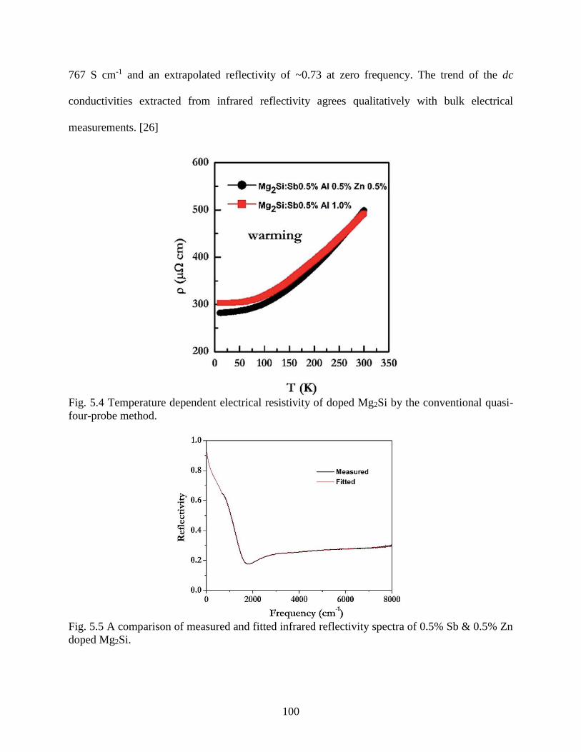
100
767 S cm-1 and an extrapolated reflectivity of ~0.73 at zero frequency. The trend of the dc
conductivities extracted from infrared reflectivity agrees qualitatively with bulk electrical
measurements. [26]
Fig. 5.4 Temperature dependent electrical resistivity of doped Mg2Si by the conventional quasi-
four-probe method.
Fig. 5.5 A comparison of measured and fitted infrared reflectivity spectra of 0.5% Sb & 0.5% Zn
doped Mg2Si.

101
Table 5.1 Summary of the dc conductivity (σ0) & carrier relaxation time (τ) of doped Mg2Si.
Compound σ0 (Scm-1) τ (s)
Mg2Si:Sb0.5%Al0.5%Zn0.5% 507 3.72 × 10⁻¹⁴
Mg2Si:Sb0.5%Al1.0% 627 3.94 × 10⁻¹⁴
Mg2Si:Sb0.5% Zn0.5% 480 3.77 × 10⁻¹⁴
Mg2Si:Sb0.5%Zn1.0% 767 5.57 × 10⁻¹⁴
The static dc conductivity increased dramatically from pure Mg2Si, due to the larger
concentration of free electrons in the conduction band by doping with Zn, Al, and Sb. From the
free electron model, dc conductivity is proportional to the electron concentration (N) and
scattering time (τ). The electron scattering time (τ) is a parameter in the Drude-Lorentz model
and can be obtained from the fitting of the reflectivity data. [28] The fitted relaxation times of
doped Mg2Si samples are tabulated in Table 5.1. The derived relaxation times of ca. 10-14 s are
consistent with other doped semiconductors. The electron concentration (N) in a doped
semiconductor is the density of the mobile electrons or holes (n- or p-doped). Since the host
crystal Mg2Si is the same for all samples, the dc conductivity depends only on the nature of the
dopants. The dramatic enhancement of the dc conductivity by the dopants is due to the
occupation of the free electron-like conduction bands. In spite of the simplicity of the Drude-
Lorentz model and the neglect of low frequency (<600 cm-1) absorption which is not accessible
by mid-infrared radiation, the results indicate that the dc conductivity can be improved by
addition of the (Zn, Al and Sb) dopants.

102
Although the trend of increasing electrical resistivity and reflectivity is the same from IR
reflectivities and four-probe conductivity measurements, the comparison of the absolute
magnitude is less satisfactory (Fig. 5.6). The dc conductivities derived from infrared reflectivity
has the same order of magnitude as the bulk measurements, but are approximately four times
smaller. One contributing factor may be the infrared beam only surveyed a very small region (20
× 20 µm2) within a couple of microns into the sample surface. This is different from the quasi-
four-probe conductivity method which is a bulk sensitive technique. At the sample surface the
atom density is less than the bulk and the chemical bonding in the surface is also stronger.
[30,31] Therefore, there are less free electrons near the sample surface thus reducing the
electrical conductivity. Although plausible, this effect cannot satisfactorily explain the
discrepancy observed here. Since the dc conductivity was obtained from the extrapolation of the
frequency dependent conductivity to zero frequency, it is not certain if the omission of
reflectivity at very low energy (i.e. <600 cm-1) may have an effect. From the past experience, we
expect that the dc conductivity derived from an IR measurement should agree within an order of
the magnitude of the value obtained from the bulk technique. [10,32] We found no systematic
error in the experiment and on the treatment of the data. In a previous study, we have also
compared the dc conductivity derived from IR reflectivities to bulk measurements on doped
Mg2Si and the agreements were favorable. [10] We suspect that the most likely source of the
disagreement may be related to a precise knowledge on the concentration of the dopants. The
doped samples used in this study were synthesized by the plasma spark sintering method. It is
very difficult to control the precise stoichiometry. Another possible source of the discrepancy
may be due to the non-uniform distribution of dopants in the sample. In a study of Sb and Bi
doped-Mg2Si, it was found by high resolution transmission microscopy (TEM) that due to the

103
limited solubility excess Sb and Bi atoms are present in the grain boundaries that may enhance
the conductivity of the bulk sample. [10] In comparison, IR measurements only examine a very
small spot of ca. 20 × 20 µm2 of the sample so this may produce different results. Finally, the
formation of a thin oxide layer on the surface may also contribute to the lower conductivity
derived from the IR experiments. A careful characterization of both samples is critical to resolve
the discrepancy.
Fig. 5.6 A comparison of electrical resistivity (ρ) extracted from infrared reflectivity spectra and
measured by the quasi-four-probe method.
The bulk electrical transport properties of the Zn, Al and Sb multi-doped Mg2Si samples
were determined by temperature dependent electrical resistivity and the Hall coefficient by the
quasi-four-probe method. The temperature dependent electrical resistivities (ρ) of doped Mg2Si
samples (Fig. 5.4) were measured with a current of 3 mA and sectional areas between 1.05 ×
0.78-1.45 × 1.01 mm2. It is found that the electrical resistivity of Mg2Si:Sb0.5%Al1.0%
increased from 300 µΩ cm to 500 µΩ cm from 10 K to 300 K. At 300 K, the electrical resistivity
in Mg2Si:Sb0.5%Zn1.0% is smaller than the other doped samples of 430-500 µΩ cm. The results
suggest that there are more free electrons in the conduction band of the other samples leading to
higher electrical conductivity. Comparing Mg2Si:Sb0.5%Zn0.5% and Mg2Si:Sb0.5%Zn1.0%, the

104
electrical resistivities were found to decrease with concentration of the Zn dopant. Since the
concentrations of Sb were the same in these two samples and the Zn atoms were expected to
occupy the Mg sites, this conductivity trend suggests that there are more mobile electrons in the
conduction band with more Zn dopants.
The measured Hall coefficients (RH) of Zn, Al, and Sb-doped Mg2Si samples are shown
in Fig. 5.7. The negative and almost constant Hall coefficients show that the multi-doped Mg2Si
materials are n-type doped semiconductors. Using the equation N = 1/(eRH), (where e is the
electron charge and RH is the Hall coefficient) the electron concentrations (N) were calculated
and are shown in Table 5.2. Possibly, Mg2Si:Sb0.5%Al1.0% has the largest electron
concentration (N) of 1.78 × 1020 cm-3, due to the high doping concentration. The electron
concentration (N) of the multi-doped Mg2Si samples of ca.1020 cm-3 is in reasonable agreement
with that estimated from the free electron model. Therefore doped-Mg2Si is a doped
semiconductor. [28] The results are supported by the low plasma frequencies of the doped
samples. The low plasma frequencies observed in the IR region is also indicative of a doped
semiconductor.

105
Fig. 5.7 Hall coefficients (RH) of doped Mg2Si samples were measured by the quasi-four-probe
method.
Table 5.2 Summary of the electron concentration (N) calculated from the Hall coefficient (RH) of
doped Mg2Si.
Compound RH (cm3C-1) N (cm-3)
Mg2Si:Sb0.5%Al0.5%Zn0.5% -5.53 × 10⁻² 1.17 × 10²⁰
Mg2Si:Sb0.5%Al1.0% -3.50 × 10⁻² 1.78 × 10²⁰
Mg2Si:Sb0.5% Zn0.5% -4.33 × 10⁻² 1.44 × 10²⁰
Mg2Si:Sb0.5%Zn1.0% -3.75 × 10⁻² 1.67 × 10²⁰
The electron effective mass can be calculated from the plasma frequency observed in the
infrared reflectivity and the electron concentration from the Hall coefficient. [33] The plasma
frequency ωp is related to the electron concentration (N) and the electron effective mass in the
sample (m*) by ωp2 = Ne2/ɛɛ0m*, where ɛ is the dielectric constant of the material, and ɛ0 is the
vacuum permittivity. [34] Therefore, the electron effective mass (m*) is inversely proportional to
the square of plasma frequency (ωp). Assuming a constant optical dielectric constant (ɛ) of 12.82
for doped Mg2Si samples, [35] the electron effective masses were calculated for all the doped
Mg2Si samples studied. As shown in Table 5.3, the effective masses of electrons in doped Mg2Si

106
samples are between 0.255me and 0.361me, where me is the mass of a free electron. The light
effective masses found in this work are comparable with previous measurements listed in Table
5.4. Electrons with lighter effective mass are easier to move in the conduction band and therefore
contribute to a higher electrical conductivity. The light effective masses i.e. 0.255me to 0.361me
of doped Mg2Si show the occupation of the free-electron-like conduction band by the excess
electron donated by the dopants. [11]
Table 5.3 Summary of the effective mass (m*) of doped Mg2Si calculated from the plasma
frequency (ωP) within the infrared reflectivity.
Compound ωP (cm-1) m*/me
Mg2Si:Sb0.5%Al0.5%Zn0.5% 1791 0.255
Mg2Si:Sb0.5%Al1.0% 1899 0.346
Mg2Si:Sb0.5% Zn0.5% 1788 0.316
Mg2Si:Sb0.5%Zn1.0% 1798 0.361
Table 5.4 Summary of the effective masses for pure and n-doped Mg2Si reported in the literature.
Pure Mg2Si 0.4me [36] 0.5me [37]
Mg2Si0.98Sb0.02 1me [36] 1.06me [10] 1.1me [38]
Mg2Si0.98Bi0.02 0.62me [10] 0.5me [39]
To define the thermoelectric properties of doped Mg2Si samples, the temperature
dependent electrical conductivity (σ), Seebeck coefficient (S), power factor (S2σ × T), and
thermal conductivity (κ) were measured up to 900 K, and the corresponding figure of merit (ZT)
was calculated. As shown in Fig. 5.8(a)-(e), the electrical conductivity of doped Mg2Si decreases

107
from 2.5 ×10⁵ S m-1 to 0.8 × 10⁵ S m-1 when the temperature is increased from 300 K to 900 K.
The highest electrical conductivity obtained in the present study is 2.6 × 10⁵ Sm-1 for
Mg2Si:Sb0.5%Zn0.5% at room temperature (300 K). The electrical conductivity of double or
multi-doped Mg2Si is substantially higher when compared to the un-doped Mg2Si (15 Sm-1). [19]
A small amount of dopants (0.5-1.0%) is found to have a dramatic impact on the electrical
conductivity. In all four multi-doped Mg2Si samples, an increase of electrical conductivity was
observed. The conductivities derived from infrared reflectivities show that the correct trend
expected from the free electron model (i.e. the conductivity of Mg2Si:Sb0.5% Al1.0% is higher
than that of Mg2Si:Sb0.5%Zn0.5%) as Al donates more electrons than Zn when substituted in the
Mg sites. The reverse was apparently observed in the bulk measurements (Fig. 5.8). This
discrepancy may be attributed to the non-homogeneity of the dopants. Moreover, the free
electron model is only a simplification and the true conductivity also depends on the effective
mass of the conducting electron, which is related to the dispersion of the occupied conduction
band. If the bulk measurements are more representative of the properties of the sample, we may
speculate that the effective mass of the conducting electrons in Mg2Si:Sb0.5%Al1.0% is heavier.
In fact, as shown in Table 5.3, the derived effective mass of the electron in
Mg2Si:Sb0.5%Al1.0% of 0.346me is heavier than that in Mg2Si:Sb0.5%Zn0.5% of 0.316me. It is
interesting to note that there is a distinctive discontinuity in the Mg2Si:Sb0.5%Al0.5%Zn0.5% at
450-500 K which will be discussed below (vide supra).

108
Fig. 5.8 Temperature dependent (a1) & (a2) electrical conductivity, (b) Seebeck coefficient, (c)
power factor, (d1) & (d2) thermal conductivity & lattice thermal conductivity, and (e) figure of
merit (ZT).
The temperature dependence of the electrical conductivity shows a discontinuity at 500
K. Even the material is metallic we used an Arrhenius-like equation ρ = ρ0 exp(-Et/kT) to
highlight the discontinuity. In the equation ρ is the electrical resistivity, ρ0 is the high
temperature resistivity, Et is the “activation” energies, k is the Boltzmann constant, and T is the
temperature. The values of Et are determined from the plot of ln(ρ) vs. (1/T). As shown in Fig.
5.8(a1) & (a2), between 450 K and 550 K, the trend of Mg2Si:Sb0.5%Al0.5%Zn0.5% does not
follow the relationship with increasing the temperature as the others. The sudden change of
activation energy (Et) further implies that a possible structure change has occurred. [40] Since

109
the high temperature crystal structure is still unknown, a definitive characterization requires a
high temperature X-ray diffraction powder diffraction study.
Throughout the temperature range studied, the Seebeck coefficients (S) of Sb, Al, and Zn
multi-doped Mg2Si samples are negative confirming that they are n-doped semiconductors, in
agreement with the Hall coefficients. The values for the temperature dependent Seebeck
coefficient (S) are quite similar for all doped samples, suggesting that the dopants play a similar
role in enhancing the Seebeck coefficient. The Seebeck coefficient increased from -90 mVK-1 to
-190 mVK-1 with increasing temperature and reached a maximum value at 900 K. The Seebeck
coefficients for the doped Mg2Si samples are comparable with the previously reported Bi, Pb,
and Sb double-doped Mg2Si. [19] For the un-doped Mg2Si sample, the Seebeck coefficient
increased initially with increasing temperature and reached the maximum value at 450 K. Above
450 K, the value of the Seebeck coefficient started to decrease.
Fig. 5.8(c) shows the calculated power factor (S2σ × T) of doped Mg2Si samples. The
general trend of the calculated temperature dependent power factor increased initially and peaked
at ~750 K and then decreased with further increase of the temperature. The maximum power
factor is due to the effect that the Seebeck coefficient (S) increases faster than the decrease in the
electrical conductivity (σ). With further increase in temperature, the power factor decreases
gradually, as the electrical conductivity (σ) becomes more important to the power factor than the
Seebeck coefficient (S). A peak power factor of 2.9 × 10⁻³ Wm-1K-2 was found at 500 K in
Mg2Si:Sb0.5%Al0.5%Zn0.5%, close to the possible structural phase transition. Fig. 5.8(d1)
shows the temperature dependent thermal conductivity of the doped Mg2Si samples. The general
trend of the thermal conductivities is to decrease with increasing temperature. This is obviously
due to the increase in phonon scatterings at higher temperature. At 310 K, the thermal

110
conductivity of Mg2Si: Sb0.5%Al0.5% Zn0.5% (5.6 Wm-1K-1) is higher than those of other
doped Mg2Si samples. However, all the thermal conductivities of doped Mg2Si samples are
lower than that of un-doped Mg2Si (6.2 Wm-1K-1). Phonon scattering becomes more efficient in
the presence of heavier dopants in the lattice. The total thermal conductivity (κtotal) can be
separated into two contributions: the lattice conductivity (κph) and the electronic conductivity
(κel). The electronic conductivity (κel) can be estimated by the Wiedemann-Franz law, where κel =
LσT (the Lorentz number (L) is 2.45 × 10⁻⁸ V2K-2). [41] The lattice thermal conductivity (κph) can
then be estimated by subtracting the electronic thermal conductivity (κel) from the total thermal
conductivity (κtotal). Considering the major contribution of lattice thermal conductivity (κph) to
the total thermal conductivity (κtotal), Fig. 5.8(d2) shows the temperature dependency of the
lattice thermal conductivity (κph). Compared to Al, the heavier Zn dopants are better phonon
scatterers, leading to lower lattice thermal conductivity. The observed trend,
Mg2Si:Sb0.5%Al0.5%Zn0.5% > Mg2Si:Sb0.5%Al1.0% > Mg2Si:Sb0.5%Zn0.5% >
Mg2Si:Sb0.5% Zn1.0%, is expected. Similarly, the lattice thermal conductivities of
Mg2Si:Sb0.5%Zn0.5% and Mg2Si:Sb0.5%Zn1.0% samples are lower than those of others
because the phonon scattering becomes more efficient in the presence of heavier Zn dopants. The
only exception is Mg2Si:Sb0.5%Al0.5%Zn0.5% which has a higher thermal conductivity than
Mg2Si:Sb0.5% Al1.0%. At this moment, we cannot provide a satisfactory explanation for this
observation. Using the information obtained above, the temperature dependent figure of merits
(ZT) were calculated (Fig. 5.8(e)). For each doped-Mg2Si sample, ZT increased significantly with
increasing temperature. A maximum ZT of 0.964 is found in Sb0.5%Zn0.5% doped Mg2Si at 880
K.
111
5.4 Conclusions
The structural information of Sb, Al, and Zn multi-doped Mg2Si powder samples
synthesized from spark plasma sintering has been obtained by angle dispersive synchrotron
radiation X-ray diffraction, infrared reflectivity, electrical and thermal conductivity
measurements. A small concentration of the dopant (0.5-1.0%) did not alter the cubic crystal
structure of the host Mg2Si, but expanded the crystal lattice noticeably. The electrical transport
properties were characterized by mid-IR reflectivity and quasi-four probe measurements.
Infrared reflectivity shows the doped semiconductor character for all the samples at room
temperature. The dc conductivities calculated from the analysis of the infrared reflectivity
spectra employing the Drude-Lorentz model are in qualitative agreement with the conventional
bulk four-probe measurements although the absolute values obtained from IR reflectivities are
consistently lower. The electron concentrations (N) were determined from the Hall coefficients
and plasma frequencies (ωP) of the infrared reflectivities. The multi-doped Mg2Si is within the
order 1020 cm-3, suggesting that all doped-Mg2Si are doped semiconductors. The effective masses
ranged from 0.255me to 0.361me showing that different dopants have a slight effect on the band
structure of Mg2Si. A maximum thermoelectric figure of merit (ZT) of 0.964 was achieved for
the Sb0.5%Zn0.5% doped Mg2Si sample at 880 K. The present study provides new results and
insight into the thermoelectric and electrical transport properties of Sb Al Zn multi-doped Mg2Si
in the temperature range of 300 K to 900 K. The information presented here may help to further
enhance the performance of Mg2Si-based thermoelectric materials.
Acknowledgements
Synchrotron work at the Canadian Light Source was made possible by support from
NSERC, NRC, CIHR, and the University of Saskatchewan. The use of the U2A beamline was

112
supported by COMPRES under NSF Cooperative Agreement EAR 11- 57758 and CDAC (DE-
FC03 03N00144). The National Synchrotron Light Source, Brookhaven National Laboratory,
was supported by the U.S. Department of Energy, Office of Science, Office of Basic Energy
Sciences under Contract No. DE-AC02- 98CH10886. The sample preparation and thermoelectric
measurements were partly supported by a Grant-in-Aid for Research (A) by the Japanese
Ministry of Education, Science, Sports, and Culture. The electrical resistivity measurement was
supported by JSPS KAKENHI Grant Number 15F15023. JZ and JST thank AUTO21 for a
research grant.
References
[1] T. Sakamoto, T. Iida, S. Kurosaki, K. Yano, H. Taguchi, K. Nishio, and Y. Takanashi,
Journal of Electronic Materials, 2011, 40, 629-634.
[2] S. Battiston, S. Fiameni, M. Saleemi, S. Boldrini, A. Famengo, F. Agresti, M. Stingaciu,
M. S.Toprak, M. Fabrizio, and S. Barison, Journal of Electronic Materials, 2013, 42,
1956-1959.
[3] T. Sakamoto, T. Iida, A. Matsumoto, Y. Honda, T. Nemoto, J. Sato, T. Nakajima, H.
Taguchi, and Y. Takanashi, Journal of Electronic Materials, 2010, 39, 1708-1713.
[4] S. You, K. Park, I. Kim, S. Choi, W. Seo, and S. Kim, Journal of Electronic Materials,
2011, 41, 1675-1679.
[5] J. Tani and H. Kido, Intermetallics, 2008, 16, 418-423.
[6] N. Wang, H. Chen, H. He, W. Norimatsu, M. Kusunoki, and K. Koumoto, Scientific
Reports, 2013, 3, 3449.
[7] Q. Chen, Q. Xie, F. Zhao, D. Cui, and X. Li, Chinese Science Bulletin, 2010, 55, 2236-
2242.
[8] G. J. Snyder, and E. S. Toberer, Nature Materials, 2008, 7, 105-114.
[9] G. H. Kim, L. Shao, K. Zhang, and K. P. Pipe, Nature Materials, 2013, 12, 719-723.
[10] N. Farahi, M. VanZant, J. Zhao, J. S. Tse, S. Prabhudev, G. A. Botton, J. R. Salvador, F.
Borondics, Z. Liu and H. Kleinke, Dalton Transactions, 2014, 43, 14983.

113
[11] M. Akasaka, T. Iida, A. Matsumoto, K. Yamanaka, Y. Takanashi, T. Imai, and N. Hamada,
Journal of Applied Physics, 2008, 104, 013703.
[12] Y. Isoda, S. Tada, T. Nagai, H. Fujiu, and Y. Shinohara, Materials Transactions, 2010, 51,
868-871.
[13] Y. Isoda, S. Tada, T. Nagai, H. Fujiu, and Y. Shinohara, Journal of Electronic Materials,
2010, 39, 1531.
[14] H. Gao, T. Zhu, X. Liu, L. Chen, and X. Zhao, Journal of Materials Chemistry, 2011, 21,
5933.
[15] Z. Du, T. Zhu, Y. Chen, J. He, H. Gao, G. Jiang, T. M. Tritt, and X. Zhao, Journal of
Materials Chemistry, 2012, 22, 6838.
[16] X. Liu, T. Zhu, H. Wang, L. Hu, H. Xie, G. Jiang, G. J. Snyder, and X. Zhao, Advanced
Energy Materials, 2013, 3, 1238.
[17] A. U. Khan, N. Vlachos, and Th. Kyratsi, Scripta Materialia, 2013, 69, 606-609.
[18] H. Le-Quoc, S. Bechu, S. Populoh, A. Weidenkaff, and A. Lacoste, Journal of Alloys and
Compounds, 2013, 546, 138-144.
[19] S. Muthiah, B. Sivaiah, B. Gahtori, K. Tyagi, A. K. Srivastava, B. D. Pathak, A. Dhar, and
R. C. Budhani, Journal of Electronic Materials, 2014, 43, 2035.
[20] G. Jiang, J. He, T. Zhu, C. Fu, X. Liu, L. Hu, and X. Zhao, Advanced Functional
Materials, 2014, 24, 3776.
[21] Y. Isoda, M. Held, S. Tada, and Y. Shinohara, Journal of Electronic Materials, 2014, 43,
2053.
[22] V. Petricek, M. Dusek, and L. Palatinus, Z. Kristallogr., 2014, 229, 345-352.
[23] A. Le Bail, H. Duroy, and J. L. Fourquet, Materials Research Bulletin, 1988, 23, 447-452.
[24] R. L. Kronig, Journal of the Optical Society of America and Review of Scientific
Instruments, 1926, 12, 547-557.
[25] A. B. Kuzmenko, Review of Scientific Instruments, 2005, 76, 083108.
[26] N. V. Morozova, S. V. Ovsyannikov, I. V. Korobeinikov, A. E. Karkin, K. Takarabe, Y.
Mori, S. Nakamura, and V. V. Shchennikov, Journal of Applied Physics, 2014, 115,
213705.
[27] M. Y. Au-Yang, and M. L. Cohen, Physical Review, 1969, 178, 1358.
114
[28] M. Fox, Optical properties of solids, 2nd edition, Oxford University Press, 2010.
[29] N. Farahi, S. Prahudev, G. A. Botton, J. Zhao, J. S. Tse, Z. Liu, J. R. Salvador, and H.
Kleinke, Journal of Alloys and Compounds, 2015, 644, 249-255.
[30] D. M. Larson, K. H. Downing, and R. M. Glaeser, Journal of Structural Biology, 2011,
174, 420.
[31] S. Mafe, J. A. Manzanares, and P. Ramirez, Physical Chemistry Chemical Physics, 2003,
5, 376.
[32] J. W. L. Wong, A. Mailman, K. Lekin, S. M. Winter, W. Yong, J. Zhao, S. V. Garimella, J.
S. John, R. A. Secco, S. Desgreniers, Y. Ohishi, F. Borondics, and R. T. Oakley, Journal
of The American Chemical Society, 2014, 136, 1070.
[33] P. Perlin, E. Litwin-Staszewska, B. Suchanek, W. Knap, J. Camassel, T. Suski, R.
Piotrzkowski, I. Grzegory, S. Porowski, E. Kaminska, and J. C. Chervin, Applied Physics
Letter, 1996, 68, 1114.
[34] P. E. Blöchl, Physical Review B, 1994, 50, 17953.
[35] D. McWilliams, and D. W. Lynch, Journal of the Optical Society of America, 1963, 53,
298.
[36] Q. Zhang, Rare Metal Materials and Engineering, 2009, 38, 166.
[37] V. K. Zaitsev, M. I. Fedorov, E. A. Gurieva, I. S. Eremin, P. P. Konstantinov, A. Y.
Samumin, and M. V. Vedernikov, Phys. Rev. B: Condens. Matter, 2006, 74, 045207.
[38] S. K. Bux, M. T. Yeung, E. S. Toberer, G. J. Snyder, R. B. Kaner, and J. P. Fleurial, J.
Mater. Chem., 2011, 21, 12259-12266.
[39] G. S. Nolas, D. Wang, and M. Beekman, Phys. Rev. B: Condens. Matter, 2007, 76,
235204.
[40] W. Ren, Y. Han, C. Liu, N. Su, Y. Li, B. Ma, Y. Ma, and C. Gao, Solid State
Communications, 2012, 152, 440-442.
[41] C. Kittel, Introduction to Solid State Physics, 8th edition, NJ:Wiley, 2005.
115
CHAPTER 6
PRESSURE-INDUCED PHASE TRANSITION AND ELECTRICAL PROPERTIES OF
THERMOELECTRIC Al-DOPED Mg2Si
Besides dopants, pressure has also been used to enhance the thermoelectric power factor.
Recently, Mg2Si nominally doped with 1% Al was compressed to 2-3 GPa and the thermal
power was found to increase significantly reaching a maximum value of 8×10⁻³ W/(K2m). In this
case, the increase in thermoelectric efficiency was also associated with an increase of electrical
conductivity. Therefore it was suggested that the Al-doped sample had become metallic between
5 and 12 GPa. A Raman spectroscopy study also provided tantalizing evidence that two possible
structural phase transitions had occurred at 5-7 GPa and 11-12 GPa. [10] To date, the structure
and cause for the enhancement of thermal power of the lightly Al-doped Mg2Si are not known.
These form the focus of this investigation.
For this chapter, we investigated the effect of pressure on the thermoelectric performance
of a sample of Al-doped Mg2Si (Mg1.99Al0.01Si). Pressure can alter the band structure of a system
but it may also induce structural transformation. At ambient pressure and temperature, Mg2Si has
a cubic anti-fluorite structure with the space group of Fm-3m. We performed in-situ X-ray
diffraction and infrared reflectivity measurements up to 17 GPa at room temperature on pure
Mg2Si and Mg2Si nominally doped with 1% Al. No structural transformation was observed in
pure Mg2Si. In contrast, a phase transition from the cubic anti-fluorite (Fm-3m) to an
orthorhombic (Pnma) structure was observed in the Al-doped Mg2Si sample at 10 GPa.
Experimentally the thermal power was found to increase significantly reaching a maximum value
of 8×10⁻³ W/(K2m) under 2-3 GPa. From our analysis of the infrared reflectivity spectra, we
concluded that the enhancement was mainly due to the increase of electrical conductivity
associated with the structural phase transition. The results show pressure can affect the structures

116
and transport properties and helps to improve the electrical conductivity. The experimentally
observed maximum thermoelectric power at 1.9 GPa is explained from the increase of the
electronic density of states at the Fermi level obtained from DFT calculations.
The results of this investigation has been published in
J. Zhao, Z. Liu, R. A. Gordon, K. Takarabe, J. Reid, and J. S. Tse, “Pressure-induced
phase transition and electrical properties of thermoelectric Al-doped Mg2Si,” Journal of Applied
Physics, vol. 118, pp. 145902, 2015.
The authors’ contributions are as follow:
J. Zhao and J. S. Tse collected ambient and high-pressure powder X-ray diffraction and
high-pressure infrared reflectivity spectrum, performed the analysis of all the
experimental data, and calculated the electronic structures from ambient to high pressure.
Z. Liu assisted in performing high-pressure infrared reflectivity experiments at BNL.
R. A. Gordon assisted in performing high-pressure powder X-ray diffraction experiments
at APS.
K. Takarabe provided the samples in Japan.
J. Reid assisted in performing ambient pressure powder X-ray diffraction experiments at
CLS.
All authors contributed to the writing and editing of the manuscripts.

117
Abstract
A recent study has shown the thermoelectric performance of Al-doped Mg2Si materials
can be significantly enhanced at moderate pressure. To understand the cause of this
phenomenon, we have performed in situ angle dispersive X-ray diffraction and infrared
reflectivity measurements up to 17 GPa at room temperature. Contrary to previous experiment,
using helium as a pressure transmission medium, no structural transformation was observed in
pure Mg2Si. In contrast, a phase transition from cubic anti-fluorite (Fm-3m) to orthorhombic
anti-cotunnite (Pnma) was observed in the Al-doped sample at 10 GPa. Infrared reflectivity
measurements show the electrical conductivity increases with pressure and is further enhanced
after the phase transition. The electron density of states at the Fermi level computed form density
functional calculations predict a maximum thermoelectric power factor at 1.9 GPa, which is in
good agreement with the experimental observation.
6.1 Introduction
Doped Magnesium silicide (Mg2Si)-based alloys have been suggested as a candidate of a
new generation of high performance and environmental friendly thermoelectric materials. [1-4]
Compared with other lead-based thermoelectric materials, Mg2Si-based alloys have the merits of
being nontoxic, sustainable, and low cost. It is well known that the efficiency of thermoelectric
materials may be increased through p- or n-type doping at ambient pressure. [5-9] A dopant can
increase the carrier concentration and mobility of the conduction electrons. Doping with heavy
atoms can affect the lattice vibrations and help to lower the thermal conductivity by increasing
the phonon-phonon scatterings. Pressure can also be used to enhance the thermoelectric power
factor. Recently, Mg2Si nominally doped with 1% Al was compressed to 2-3 GPa, and the
thermal power was found to increase significantly reaching a maximum value of 8×10⁻³

118
W/(K2m). In this case, the increase in the thermoelectric efficiency is associated with an increase
of electrical conductivity, and it was suggested that the Al-doped sample became metallic
between 5 and 12 GPa. A Raman spectroscopy study also hinted at two possible structural phase
transitions at 5-7 GPa and 11-12 GPa. [10] To date, the structure and the cause for the
enhancement of the thermal power of the lightly Al-doped Mg2Si are still not known. This is the
focus of this investigation.
At ambient pressure and temperature, Mg2Si has a cubic anti-fluorite structure (space
group Fm-3m) and is a semiconductor with a small indirect band gap of 0.6 eV. [11] Using
energy dispersive X-ray diffraction and silicone oil as the pressure medium, it was reported that
Mg2Si underwent a structural transition to an orthorhombic anti-cotunnite structure with space
group Pnma at 7.5 GPa. Further compression led to a hexagonal Ni2In-type P63/mmc structure at
21.3 GPa. [12,13] The high pressure structural phase transition behavior of pure Mg2Si was re-
investigated by Zhu et al. with an angle dispersive diffraction using NaCl as the pressure
transmitting medium. [14] A phase transition from the anti-fluorite structure to the monoclinic
structure was reported at 11.1 GPa. No further phase transition was found up to 37.5 GPa.
The discrepancy between the two diffraction measurements is unsettling and raises the
question on the true identity of compressed Mg2Si and the role of the pressure transmission
medium to the crystal structure. This is further complicated by experimental resistivity
measurements of undoped Mg2Si, where three distinct regimes separated at 7, 12, and 22 GPa
were observed, but Mg2Si remained a semiconductor with the hint of eventual metallization at
pressure exceeding 22 GPa. [15] Since theoretical calculations have predicted that the high
pressure anti-cotunnite and Ni2In structures are metallic, [16,17] the resistivity measurements
clearly show there is no insulator → metal transition below 7 GPa. As will be shown and

119
discussed below, and contrary to earlier reports, [12,13] the present study reveals no structural
phase transition in pure Mg2Si up to 18 GPa. However, a structural phase transition was found in
Al-doped Mg2Si at 11 GPa.
Since the reflectivity is related to the dielectric function, frequency dependent optical
conductivity can be extracted from the analysis. Static (dc) conductivities can be obtained by
extrapolation to zero photon energy. In-situ high pressure far and mid-infrared reflectivity
measurements have been performed on a nominal 1 at. % Al-doped Mg2Si sample and compared
to the results from bulk measurements. [10] The general trend that the electrical conductivity
increases with pressure is the same as that found in previous measurements. Data analysis is
complemented with theoretical density functional band structure calculations, which reveal a
partially filled mid-gap band due to localized electronic interactions between the Al dopant with
the surrounding host atoms is responsible for the enhancement of the thermopower.
The objective of this paper is to investigate the high pressure structure and the
relationship to the transport properties of Al-doped Mg2Si. For comparison, we have also
examined the structure of pure Mg2Si. For this purpose, room-temperature high resolution
synchrotron angle dispersive synchrotron X-ray diffraction experiments up to 14.7 GPa using
helium as the quasi-hydrostatic pressure-transmitting medium. Compared to silicone oil and
NaCl, helium has the advantage of remaining in the liquid state at higher pressure and, therefore,
able to maintain the isotropic strain of the sample in the diamond anvil cell (DAC).
The layout of the paper is as follows. First, details on the experimental procedure will be
described. Diffraction results on pure Mg2Si will be then compared with earlier studies. New
results on the structure and structural transformation of Al-doped Mg2Si under pressure will then
120
be presented. This is followed by a discussion on the electrical properties extracted from the
analysis of far and mid-IR reflectivity spectra. Comparison of the electrical conductivity with the
variation of theoretical electronic density of states (DOS) is then made. The paper concludes
with a proposed mechanism for the increase in thermopower under pressure.
6.2 Experiment
Electron microprobe analysis: Powder Mg2Si with a purity of 99.5% was purchased from
Alfa Products. Mg2Si doped with nominal 1 at. % of Al was synthesized by spark plasma
sintering technique. To quantitatively examine the chemical compositions of Al-doped Mg2Si
powder samples, elemental analysis was performed on a JEOL 8600 Superprobe electron
microprobe analyzer operating at 15 kV and 50 nA. The beam diameter was 5mm. Dwell time on
the peak was 60 s. SPI metals were used as standards for each element. Random sites on a
compressed powder sample were selected and analyzed to give an unbiased sampling of
compositions.
High-pressure powder x-ray diffraction measurement: The ambient powder diffraction
patterns for pure and 1% Al-doped Mg2Si were measured at the CMCF beamline, Canadian
Light Source (CLS). High-pressure X-ray diffraction experiments were performed at Sector 20,
Advanced Photon Source (APS) at the Argonne National Laboratory, using synchrotron radiation
(λ=0.47685Å). A DAC was used to generate the pressure. The powder sample was placed in the
hole of a stainless steel gasket between the diamond anvils and then loaded with helium as the
pressure transmitting medium. A ruby sphere was placed with the powder sample with the
pressure determined from the peak shift of the ruby R1 and R2 fluorescence lines. [18] The
maximum pressure studied was 14.7 GPa for pure Mg2Si and 16.6 GPa for Al-doped Mg2Si. The

121
diffraction patterns were analyzed using the JANA 2006 software package and the lattice
parameters were determined by Le Bail fit. [19,20]
High-pressure infrared reflectivity measurement: High-pressure infrared reflectance
spectra on 1% Al-doped Mg2Si sample were measured at the side-station of the U2A beamline at
the National Synchrotron Radiation Facility, Brookhaven National Laboratory. The mid-infrared
spectra were recorded on a Bruker Vertex 80v FTIR spectrometer and a Hyperion 2000 IR
microscope attached with a liquid nitrogen cooled HgCdTe detector.
The far-infrared spectra were recorded by a vacuum liquid helium cooled bolometer
detector. Powder sample of Al-doped Mg2Si was prepared and loaded into a stainless steel gasket
placed between two 300 µm culets of a Sintek mini type IIa diamond anvil cell. A stainless steel
gasket was preindented in the diamond anvil cell, and a 100 µm hole was drilled in the center of
the indentation to serve as a sample chamber. Prior to the loading of the sample, the reflected
power intensities of air-diamond base (Id) and air-diamond culet (Ic) interfaces were measured at
each pressure point. This process allowed us to minimize the error due to the intensity difference
between diamond culet and base. After loading the sample and closing the DAC, the power
intensity reflected from the air-diamond base (Id) was measured again, and subsequently, the
power intensity reflected from the sample-diamond interface (Isd) was measured.
The reflectivity of sample-diamond interface (Rsd) was calculated as
Rsd=(Isd/Id)×(Id/Ic)×(Ic/I0), where I0 is the power intensity reflected from gold foil. And Ic/I0 is a
constant of 0.185. All the spectral data were collected at a resolution of 4 cm-1 and accumulated
for 512 scans. Once again, the fluorescence from a ruby crystal placed in the powder sample was
used for pressure calibration.

122
Frequency dependent optical conductivity was obtained by Kramers-Kronig (K-K)
analysis of the data obtained from normal incidence reflectivity measurements. [21] The data
were subsequently fitted using a variational K-K constrained dielectric function, as implemented
in the RefFIT code. [22] After the correction for the diamond contribution, the frequency
dependent optical conductivity is derived from fitting to a Drude-Lorentz (DL) model, and the dc
conductivity is obtained from the extrapolation to zero frequency.
Electronic structure calculations: First Principles electronic calculations were performed
using density functional theory (DFT) within the Perdew-Burke-Ernzerh (PBE) of
parameterization of the generalized gradient approximation (GGA) as implemented in the
Vienna ab initio simulation package (VASP) code. [23-26] To obtain accurate band gap energy
of pure Mg2Si at ambient and high pressure, additional calculations were performed with the GW
approximation (GWA), which utilized the one-particle Green’s function and screened Coulomb
interaction W to account for the effect of electrons to the electronic band structure. [27,28] For
all calculations, the projector-augmented wave (PAW) [29,30] potentials constructed from the
generalized PBE functional were used with 3s23p1, 3s23p2, and 2p63s2 as valence electrons for
the Al, Si, and Mg atoms, respectively. A 4×4×4 k-points mesh was used for total density of
states (TDOS) and projected density of states (PDOS) calculations. A 1 at. % Al doped Mg2Si
was constructed from a 2×2×2 supercell of the crystal where one of the Mg atoms is replaced
with Al (i.e., Mg63Si32Al).
6.3 Results and Discussion
Room-temperature high resolution synchrotron angle dispersive X-ray diffraction
patterns of pure Mg2Si were measured up to 14.7 GPa (Figure 6.1) using helium as the pressure
medium. It was shown in a recent report comparing argon and silicone oil as the pressure

123
transmission medium. [31,32] The linewidth of diffraction pattern in silicone oil is substantially
broadened above 10 GPa. Compared to silicone oil and NaCl, helium has the advantage of
remaining in the liquid state at higher pressure and, therefore, able to maintain the isotropic
strain of the sample in the DAC. Furthermore, the diffraction patterns will be not interfered by
the diffraction lines of NaCl. It is unlikely the helium will occupy the empty sites in Mg2Si.
Since Mg2Si is built from a FCC Si lattice with Mg in the octahedral sites, the only possible site
that helium atoms may diffuse into is the tetrahedral site. However, the powder diffraction
pattern of pure Mg2Si was measured independently without a medium. The cubic unit cell
parameter determined at ambient pressure agrees well with the results obtained in the DAC
extrapolated to zero pressure with helium as the medium. In addition, the lattice constant and
volume fitted with the 3rd order Birch-Murnaghan equation of state (red lines) are also in
reasonable agreement with results of theoretical calculations (Figure 6.2). Therefore, there is no
evidence that the helium can incorporate in the crystal lattice.
124
Fig. 6.1 Angle dispersive X-ray diffraction patterns of pure Mg2Si at selected pressures measured
at room temperature.
Fig. 6.2 (a) Lattice parameters of pure Mg2Si as a function of pressure obtained in the present
study and compared with previous works. (b) The volume per formula of pure Mg2Si as a
function of pressure and compared with previous works. The red color lines are fits to 3rd order
Birch-Murnaghan equation of state.
125
It is important to point out that we observed no impurity peaks that can be attributed to
MgO. The lattice constants were determined from full profile Le Bail fit to the diffraction peaks
between 7º to 18º using the JANA 2006 software package. All the X-ray diffraction patterns can
be indexed readily to the ambient pressure cubic anti-fluorite (CaF2) structure with space group
Fm-3m. The Miller indices (hkl) of the Bragg peaks are identified as (111), (200), (220), (311),
(222), and (400) reflections with increasing scattering angles. No structural phase transition was
found up to 14.7 GPa, the highest pressure studied. All diffraction patterns display the same
profile except shifts of the Bragg peaks to higher angles with increasing pressure. The derived
lattice parameters and unit cell volumes as a function of pressure were reported in Figures 6.2(a)
and 2(b), respectively. The pressure coefficient for the cubic lattice determined from the
experiment is -0.045Å/GPa. The lattice parameters are in good accord with previous results by
Zhu et al. and Hao et al. within the overlapping pressure region up to 7.5 GPa. [13]

126
Fig. 6.3 GW band structures of pure Mg2Si at 0.1, 4, 8, and 11 GPa.
To examine the electronic property of Mg2Si at high pressure, theoretical density
functional calculations with the PBE function were performed at 0, 4, 8, and 11 GPa (Figure
6.3). The calculated band structures were corrected for electron correlation effect as GW-
correction. [40] Obviously, Mg2Si is a semiconductor with the small band gap over this pressure
range. The GW band gaps are 0.62, 0.46, 0.41, and 0.30 eV at 0, 4, 8, and 11 GPa, respectively.
The theoretical results agree with the resistivity measurements that show Mg2Si is an insulator at
least up to 22 GPa. Together with the electrical measurements, structural transitions to the high
pressure anti-cotunnite and Ni2In phases at 7 and 11 GPa can be ruled out.
Experimental angle dispersive synchrotron radiation X-ray diffraction patterns of 1% Al-
doped Mg2Si were measured as a function of pressure up to 16.6 GPa (Figure 6.4). Again crystal
lattice parameters were extracted from full profile of the diffraction patterns. At 0.9 GPa,
diffraction peaks located at 7.5º, 8.7º, 12.3º, 14.5º, 15.1º, and 17.5º are indexed to (111), (200),

127
(220), (311), (222), and (400) reflections of the cubic anti-fluorite structure of Mg2Si. Below
10.5 GPa, the diffraction patterns of 1% Al-doped Mg2Si are similar to pristine Mg2Si. At low
pressure, a small amount of Al dopant is not expected to affect the crystal lattice of the host
significantly.
Fig. 6.4 Room temperature angle dispersive x-ray diffraction patterns of 1% Al-doped Mg2Si at
selected pressures.
The unit cell of Al-doped Mg2Si is slightly larger than the pure Mg2Si below 2 GPa. This
suggests the Al dopants should occupy the Mg sites in the crystal structure. Therefore, under
ambient conditions and low Al-doping concentration, Mg2Si is expected to be an n-type
semiconductor. This assignment is in agreement with the negative value of Hall coefficient
reported. [10] The cubic structure is maintained up to 10.5 GPa. Interestingly, the derived
pressure coefficient for the cubic lattice of 0.023 Å/GPa is substantially smaller than in the pure

128
sample. This observation indicates that even at 1% doping the Al-Mg2Si crystal lattice is more
resilient to compression. Figures 6.5 (a) and (b) show the pressure dependence of the lattice
parameters and the unit cell volumes (Figure 6.5). At ambient pressure, the cell parameter of the
cubic anti-fluorite structure (Fm-3m) of 6.2878(9) Å is reduced to 6.0261(11) Å at 10.5 GPa.
Concomitantly, the cell volume per formula unit decreased from 62.15(12) Å3 to 54.71(12) Å3. It
is interesting to note that the ambient pressure lattice constant obtained here with high resolution
synchrotron radiation is noticeably shorter than the earlier report of 6.396(1) Å. [10] As will be
discussed below (vide supra), this difference may have important implications on the transport
properties. The experimental results conclusively indicated the anti-fluorite structure (Fm-3m) of
Al-doped Mg2Si is stable up to 10.5 GPa.

129
Fig. 6.5 (a) Lattice parameters of anti-fluorite (Fm-3m), and anti-cotunnite (Pnma) phases for Al-
doped Mg2Si and pure Mg2Si as a function of pressure. (b) The volume per formula of Al-doped
Mg2Si and pure Mg2Si as a function of pressure.
Above 11.9 GPa, three new diffraction peaks marked by arrows in Figure 6.4 have
emerged, indicating a change in the crystal structure. The new peaks at 10.7º, 11.4º, and 13.5º
can be indexed to an orthorhombic anti-cotunnite (Pnma) structure with a=5.8282(20) Å,
b=4.6313(12) Å, and c=6.6059(23) Å. The strong diffraction peaks at 7.5º, 8.7º, and 12.3º can
still be assigned to the cubic anti-fluorite structure (Fm-3m), indicating that the orthorhombic
anti-cotunnite (Pnma) structure co-exists with the cubic anti-fluorite structure (Fm-3m) at this
pressure. The amount of the cubic structure decreased with increasing pressure and eventually
130
vanished at 16.6 GPa. Concomitantly, the diffraction peaks around 10.7º, 11.4º, and 13.5º,
corresponding to orthorhombic anti-cotunnite (Pnma) structure, increased gradually and became
dominant. Therefore, the diffraction results show unambiguously a structural phase transition of
Al-doped Mg2Si had occurred around 11.9 GPa and was completed at 16.6 GPa. This structural
transformation is accompanied by a large volume reduction of almost 23%. The experimental
equation of state (volume vs. pressure) shown in Figure 6.5 indicates that the anti-cotunnite
phase is more compressible than the cubic structure.
In the previous high energy dispersive X-ray diffraction study of pure Mg2Si using
silicone oil as the pressure medium, the same Fm-3m to Pnma transition was observed at 7.5 GPa
where the volume collapsed from the cubic structure of 56.3 Å3/f.u to Pnma of 49.4 Å3/f.u, a
reduction of 12.3%. [13] The transition in Al-doped Mg2Si was observed at a higher pressure of
10 GPa, and the volume reduced by 18% from the cubic phase of 55 Å3/f.u to Pnma 45 Å3/f.u.
Therefore, the volume changes are comparable.
The behavior of pressure-induced structural phase transition for Al-doped Mg2Si is
different from pristine Mg2Si which shows no structural transition up to 14.7 GPa. The phase
transformation is related to the Al dopant in the crystal structure. A larger atomic size of Al
compared to Mg expanded the cubic crystal lattice at low pressure, resulting in a smaller pressure
coefficient (vide supra). We speculate this mismatch in the atomic size helps to promote the
structural transformation at high pressure.
131
Fig. 6.6 Infrared reflectivity spectra of 1% Al doped Mg2Si under different pressures.
The measured reflectivities from ambient to 14 GPa are shown in Figure 6.6. Even at
ambient pressure, the IR reflectivity shows a Drude-like behavior at a low frequency implying a
metallic-like behaviour. In Mg2Si, the valence bands are completely filled, the electrons provided
by the Al dopants must occupy the conduction band. By definition, the partial occupation of the
conduction band is a metal. A practical definition for a metal is that the electrical conductivity
should decrease with temperature. Previous experiment [10] shows that the electrical
conductivity of Al-doped Mg2Si indeed decreases with temperature, an indication of a metallic-
like behaviour. We recognize that doped Mg2Si are often referred as a semiconductor. However,
we believe it is just a matter of semantic. This point is highlighted from a comparison of the
reflectivity of pure and Al-doped Mg2Si at zero pressure (Figure 6.7). In comparison to the flat
and featureless reflectivity, typical of a semiconductor of pure Mg2Si, the extrapolated
reflectivity at zero frequency of the doped sample is almost 0.4. On closer examination (inset of
Fig. 6.6), it is observed that the reflectivity rose gradually from ambient pressure to about 10.5
GPa. From 8.5 to 10.5 GPa, there is a noticeable jump in the reflectivity from 0.32 to 0.58.

132
Beyond this pressure, the reflectivities increase rapidly and reach 0.75 at 600 cm-1 at 14.1 GPa.
This is to be compared with reflectivity close to unity at zero frequency for a good metal, such as
copper or aluminum. Qualitatively, the observed trend in the reflectivity parallels that of the bulk
measurements reported previously. [10] It was reported that the electrical resistivity decreases
(conductivity increases) almost by one order of magnitude from 0 to 1 GPa but became more
gradual from 1 to 8 GPa. However, the rapid drop (rise) in the electrical resistivity (conductivity)
at low pressure reported earlier by quasi-4-probe method [10] was not so obvious in the infrared
reflectivity measurements.
Fig. 6.7 Comparison of the infrared reflectivity spectra of 1% Al-doped Mg2Si and pure Mg2Si
under ambient conditions.
The frequency dependent conductivity (optical conductivity) can be obtained by
performing a K-K analysis of the reflectivity data using the RefFIT code. [22] The procedure is
as follows: the optical conductivity obtained from a variational K-K transformation is fitted to a
DL model and the dc conductivity is estimated by extrapolation to zero frequency. A typical
result shows in Figure 6.8, illustrating the quality of the fitting procedure. In the Figure, the
original and the fitted infrared reflectivity spectra at 10.5 GPa are compared. The dc
conductivities are obtained with this procedure (Figure 6.9), where an almost linear dependence

133
with pressure. The dc conductivity is 80 Scm-1 at ambient pressure and reaches 300 Scm-1 at 14.1
GPa, a fourfold increase. It is apparent that there are two “plateau” regions in the conductivity at
ca. 6 and 10 GPa. However, due to the simplicity of the Drude-Lorentz model and the limited
low frequency range accessible by IR radiation, there is not enough firm data to make a
definitive statement. Nevertheless, the results indicate that the conductivity of Al-doped Mg2Si
can be improved significantly by increasing pressure.
Fig. 6.8 A comparison of measured and fitted infrared reflectivity spectra of 1% Al doped Mg2Si
at 10.5 GPa.

134
Fig. 6.9 The change in dc conductivities of 1% Al-doped Mg2Si changes with pressure.
In the free electron model, the electron scattering relaxation time (τ) is related to be the
electrical conductivity. This parameter can be extracted from the fitting the reflectivity data to
the Drude-Lorentz model. [33] The relaxation times obtained at different pressures are
summarized in Table 6.1. The derived relaxation times of ca. 10-14 s is consistent with other
doped semiconductors.
To understand the mechanism for the pressure enhancement of the thermoelectric power
factor, theoretical density functional calculations were performed at several pressures using a
Mg63Si32Al1 supercell model (vide supra). No GW corrections were needed since the model
system is already metallic-like. The aim of the calculations was to investigate the total and
projected DOS and how they affect the thermopower with pressure. The results of the
calculations are shown in Figure 6.10.

135
Fig. 6.10 Total density of states and projected density of states for Al-doped Mg2Si at (a) 0.1
GPa, (b) 0.9 GPa, (c) 1.9 GPa, (d) 3.3 GPa, (e) 4.9 GPa, (f) 6.4 GPa, (g) 8.4 GPa, and (h) 10.3
GPa.

136
Table 6.1 Summary of dc conductivity (σ) and carrier relaxation time (τ) of 1% Al-doped Mg2Si
changing with the function of pressure.
Pressure (GPa) σ (Scm-1) τ (s)
0.3 90 2.9×10⁻¹⁴
0.6 81 6.1×10⁻¹⁴
0.9 102 6.3×10⁻¹⁴
2.0 134 7.1×10⁻¹⁴
2.3 128 9.3×10⁻¹⁴
3.3 135 7.3×10⁻¹⁴
3.7 143 7.4×10⁻¹⁴
4.3 141 8.0×10⁻¹⁴
4.8 147 6.7×10⁻¹⁴
5.3 143 6.3×10⁻¹⁴
5.9 164 6.2×10⁻¹⁴
6.8 193 6.7×10⁻¹⁴
7.7 213 6.5×10⁻¹⁴
8.5 213 4.6×10⁻¹⁴

137
9.6 218 2.8×10⁻¹⁴
10.5 229 2.5×10⁻¹⁴
11.4 259 1.4×10⁻¹⁴
12.5 284 0.7×10⁻¹⁴
13.4 292 0.6×10⁻¹⁴
14.1 293 0.4×10⁻¹⁴
At zero pressure, Al-doped Mg2Si already has a metallic-like behaviour. The Al impurity
produced a distinct narrow band with very high DOS located between the valence and
conduction band of the Mg2Si host. The sharp feature is due to localized interactions between the
Al dopant with Mg and Si electronic states of the host.
From 0.1 to 3.3 GPa, a localized energy band was predicted to situate between the
original gap of pristine Mg2Si. As the pressure was increased, this electronic band broadened and
became more “free-electron” like. This trend explains the observed increase in metal-like
behaviour, as well as the higher electrical conductivity and infrared reflectivities. It is known that
the thermoelectric power factor is dependent on both the density of states and the derivative at
the Fermi energy. [33,34] A significant increase in the thermoelectric power factor is usually
caused by the existence of a sharp localized DOS at the Fermi level. [35,36] The calculate DOS
at the Fermi level N(Ef) was found to decrease from 19 electronic states/eV/spin at 0.1 GPa to 9
electronic states/eV/spin at 10.3 GPa. In comparison, the slope of the density of states

138
(dN(E)/dE)│Ef increased from 561 states/eV2 at zero pressure to a maximum value of 604
states/eV2 at 1.9 GPa and then decreased rapidly to 104 states/eV2 at 10.3 GPa (Figure 6.11 and
Table 6.2). On theoretical ground, it is expected the effect of N(Ef) and (dN(E)/dE)│Ef will result
in an initial increase in the thermopower to 1.9 GPa then followed by a rapid drop. The predicted
trend is in qualitative agreement with the measured thermopower, which has a maximum at 2.3
GPa. [10]
Fig. 6.11 (a) The derivative of total density of states (dN(E)/dE)│Ef. (b) The magnitude of total
density of states at the Fermi level N(Ef) for Al-doped Mg2Si as a function of pressure.
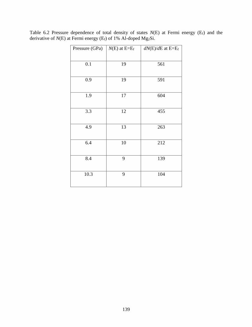
139
Table 6.2 Pressure dependence of total density of states N(E) at Fermi energy (Ef) and the
derivative of N(E) at Fermi energy (Ef) of 1% Al-doped Mg2Si.
Pressure (GPa) N(E) at E=Ef dN(E)/dE at E=Ef
0.1 19 561
0.9 19 591
1.9 17 604
3.3 12 455
4.9 13 263
6.4 10 212
8.4 9 139
10.3 9 104

140
Although the trend of increasing electrical conductivity with pressure is the same as
obtained from IR reflectivities and four-probe conductivity measurements, [10] the comparison
of the absolute magnitude is less satisfactory. One contributing factor may be the infrared beam
that only surveyed a very small region (20×20 µm2) and penetrated only a few microns into the
sample surface. This process is different from the quasi-four-probe conductivity method, which
is a bulk sensitive technique. At the sample surface, the atom density is less than the bulk, and
the chemical bonding in the surface is also stronger. [37,38] Therefore, there are fewer free
electrons near the sample surface, thus reducing the electrical conductivity. Although plausible,
this effect cannot satisfactory explain the discrepancy observed here. Since the dc conductivity
was obtained from the extrapolation of the frequency dependent conductivity to zero frequency,
it is not certain if the omission of reflectivity at very low energy (i.e.,<200 cm-1) may have an
effect. From past experience, we expect the conductivity derived from an IR measurement
should agree within an order of the magnitude of the value obtained from the bulk technique.
[39,40] We found no systematic error in the experiment, nor in the treatment of the data. In a
previous study, we have compared the dc conductivity derived from IR reflectivities to bulk
measurements on doped Mg2Si and the agreements were favorable. [39] We suspect the most
likely source of the disagreement may be related to the differences in the concentration of the
dopant on the surface. The Al-doped Mg2Si used in this study was synthesized by plasma spark
sintering method. With this technique, this is difficult to control the precise stoichiometry and the
homogeneity of the doped samples. As mentioned above, compared to the pure crystal, the cubic
lattice constant of doped Mg2Si is expanded by the inclusion of the Al dopants. The unit cell
parameter for the sample used in this study is 6.2878(9) Å, which is noticeably shorter than the

141
reported lattice constant of 6.396(1) Å on a previous sample. A larger unit cell suggests the
concentration of Al in the sample used in the earlier investigate is probably higher.
Since Al-doped Mg2Si is n-doped with the Al atoms providing electrons into the
conduction band, a higher Al content will increase the carrier concentration and enhance the
electrical conductivity. It is noteworthy that from the diffraction patterns, unlike in the previous
study, the Al-doped Mg2Si sample used in this study is free of MgO and other impurities.
Another possible source of the discrepancy may be due to non-uniform distribution of Al in the
sample.
Fig. 6.12 Scanning electron microscopy (SEM) image of Al-doped Mg2Si powder sample.
In a study of Sb and Bi doped-Mg2Si, it was found by high resolution transmission
microscopy (TEM) that due to the limited solubility excess Sb and Bi atoms are present in the
grain boundaries that may enhance the conductivity of the bulk sample. [39] In comparison, IR
measurements only examine a very small spot of the sample so this may produce different
results. A careful characterization of both samples is critical to resolve the discrepancy. For this
purpose, we examined the chemical compositions of the Al-doped Mg2Si sample using scanning

142
electron microscopy (SEM). The chemical compositions of several randomly chosen spots on the
surface of a compressed sample were analyzed (Figure 6.12). The results of the analysis are
summarized in Table 6.3, showing that the doping is highly non-uniform. The concentrations of
the doped Al can vary between a minimum of 0.27% at site #4 to a maximum of 1.42% at site
#6. The large inhomogeneity in the dopant concentrations will certainly affect the local
electronic. Since infrared reflectivity only probes a small spot, we believe that this is the main
reason for the discrepancy between the electrical conductivity determined from infrared
reflectivities and the bulk measurements.
Table 6.3 The chemical compositions of Al-doped Mg2Si powder sample were quantitatively
determined by the electron microprobe analysis.
Position Si (wt. %) Al (wt. %) Mg (wt. %)
1 35 0.48 63
2 33 0.36 64
3 35 0.57 64
4 34 0.26 65
5 35 0.39 65
6 34 1.4 63
7 32 0.62 65
143
6.4 Conclusion
The structural transformation and electrical conductivity of a nominally 1 at. % Al-doped
Mg2Si sample synthesized from spark plasma sintering have been investigated by angle
dispersive synchrotron radiation X-ray diffraction and infrared reflectivity up to 16.6 GPa at
room temperature. Contrary to two earlier reports, no structural transformation was observed in
pure Mg2Si up to 15 GPa when helium was used as the quasi-hydrostatic pressure transmission
medium. The electronic band structures of pure Mg2Si were calculated at selected pressures with
density functional theory including the correction for electron correlation effect with the GW
approximation. It is found that the band gap of Mg2Si does not close at 11 GPa. The theoretical
result is consistent with electrical resistivity measurements, which show that Mg2Si remains an
insulator at least up to 22 GPa. Both studies contradict the reported structural phase transition to
metallic anti-cotunnite and Ni2In phases 7 and 11 GPa, respectively. However, in Al-doped
Mg2Si, a structural phase transition from the cubic anti-fluorite to the anti-cotunnite structure
was found to occur around 11.9 GPa. Infrared reflectivity show the Al-doped Mg2Si already has
a metallic-like behavior under ambient conditions.
The dc conductivities at high pressure were calculated from the analysis of the infrared
reflectivity spectra employing the Drude-Lorentz model. In agreement with bulk four-probe
measurements, the electrical conductivity was found to increase with pressure as the sample
became more metallic-like. However, the values of the dc conductivity derived from IR
reflectivities are consistently lower. We attribute this difference to the difference in the
stoichiometry of the sample used in the experiment and non-uniform doping. Theoretical density
functional calculations reveal the presence of a mid-gap localized electronic band below 3.3
GPa. The sharp mid-gap DOS is the result of hybridization between the electron orbitals of the

144
host elements with the dopant. As the pressure is increased further, the localized band broadened
and the profile became more free-electron like. The derivative of the electron density of states
N(E) at the Fermi energy (Ef) is found to maximize at 1.9 GPa. Thus, the theory predicted a
maximum thermoelectric power factor, which is in agreement with the experimental observation
at 2-3 GPa.
The present study provides new results and insight on the high pressure structures and
transport properties of pure and Al-doped Mg2Si. The diffraction experiments found no phase
transition at 6-7 GPa, suggested by the Raman study. [10] However, transformation to an
orthorhombic anti-cotunnite (Pnma) structure is confirmed at 11 GPa. The information obtained
here may help to further enhance the performance of Mg2Si-based thermoelectric materials.
Acknowledgements
Ambient pressure synchrotron X-ray diffraction experiments were performed at the
CMCF beamline, Canadian Light Source, which was made possible by support from NSERC,
NRC, CIHR, and the University of Saskatchewan. High pressure synchrotron X-ray diffraction
experiments were performed at sector 20 at the Advanced Photon Source, supported by the U.S.
Department of Energy-Basic Energy Sciences, the Canadian Light Source and its funding
partners, the University of Washington, and the Advanced Photon Source. Use of the Advanced
Photon Source, an Office of Science User Facility operated for the U.S. Department of Energy
(DOE) Office of Science by Argonne National Laboratory, was supported by the U.S. DOE
under Contract No. DE-AC02-06CH11357. The use of U2A beamline was supported by
COMPRES under NSF Cooperative Agreement EAR 11-57758 and CDAC (DEFC03
03N00144). The National Synchrotron Light Source, Brookhaven National Laboratory, was
supported by the U.S. Department of Energy, Office of Science, Office of Basic Energy Sciences
145
under Contract No. DE-AC02-98CH10886. The electron microprobe analysis was supported by
the Microscopy Lab, Department of Geological Sciences, University of Saskatchewan. J.Z. and
J.S.T. thank AUTO21 for a Research Grant and to T. Bonli for the SEM measurements and J.
Smith of HPCAT, Advanced Photon Source, for assistance with the high pressure diffraction
experiments. We thank S. Tkachev for the help in using the gas-loading system, which is
supported by GSECARS and COMPRES. APS is a user facility operated for the DOE Office of
Science by ANL under Contract No. DE-AC02- 06CH11357.
References
[1] T. Sakamoto, T. Iida, S. Kurosaki, K. Yano, H. Taguchi, K. Nishio, and Y. Takanashi, J.
Electron. Mater., 2011, 40, 629-634.
[2] S. Battiston, S. Fiameni, M. Saleemi, S. Boldrini, A. Famengo, F. Agresti, M. Stingaciu,
M. S. Toprak, M. Fabrizio, and S. Barison, J. Electron. Mater., 2013, 42, 1956-1959.
[3] T. Sakamoto, T. Iida, A. Matsumoto, Y. Honda, T. Nemoto, J. Sato, T. Nakajima, H.
Taguchi, and Y. Takanashi, J. Electron. Mater., 2010, 39, 1708-1713.
[4] S. You, K. Park, I. Kim, S. Choi, W. Seo, and S. Kim, J. Electron. Mater., 2012, 41, 1675-
1679.
[5] J. Tani and H. Kido, Intermetallics, 2008, 16, 418-423.
[6] N. Wang, H. Chen, H. He, W. Norimatsu, M. Kusunoki, and K. Koumoto, Sci. Rep., 2013,
3, 3449.
[7] Q. Chen, Q. Xie, F. Zhao, D. Cui, and X. Li, IEEE Comput. Soc., 2009, 22, 338-341.
[8] G. J. Snyder and E. S. Toberer, Nat. Mater., 2008, 7, 105-114.
[9] G. H. Kim, L. Shao, K. Zhang, and K. P. Pipe, Nat. Mater., 2013, 12, 719-723.
[10] N. V. Morozova, S. V. Ovsyannikov, I. V. Korobeinikov, A. E. Karkin, K. Takarabe, Y.
Mori, S. Nakamura, and V. V. Shchennikov, J. Appl. Phys., 2014, 115, 213705.
[11] M. Y. Au–Yang and M. L. Cohen, Phys. Rev., 1969, 178, 1358.
[12] J. Hao, Z. Guo, and Q. Jin, Solid State Commun., 2010, 150, 2299-2302.

146
[13] J. Hao, B. Zou, P. Zhu, C. Gao, Y. Li, D. Liu, K. Wang, W. Lei, Q. Cui, and G. Zou, Solid
State Commun., 2009, 149, 689-692.
[14] F. Zhu, X. Wu, S. Qin, and J. Liu, Solid State Commun., 2012, 152, 2160-2164.
[15] F. Yu, J. X. Sun, W. Yang, R. G. Tian, and G. F. Ji, Solid State Commun., 2010, 150, 620.
[16] W. Ren, Y. Han, C. Liu, N. Su, Y. Li, B. Ma, Y. Ma, and C. Gao, Solid State Commun.,
2012, 152, 440-442.
[17] B. H. Yu and D. Chen, Chin. Phys. B, 2011, 20, 030508.
[18] H. K. Mao, J. Xu, and P. M. Bell, J. Geophys. Res., 1986, 91, 4673-4676.
[19] V. Petricek, M. Dusek, and L. Palatinus, Z. Kristallogr., 2014, 229, 345-352.
[20] A. Le Bail, H. Duroy, and J. L. Fourquet, Mater. Res. Bull., 1988, 23, 447-452.
[21] R. L. Kronig, J. Opt. Soc. Am. Rev. Sci. Instrum., 1926, 12, 547-557.
[22] A. B. Kuzmenko, Rev. Sci. Instrum., 2005, 76, 083108.
[23] G. Kresse and J. Hafner, Phys. Rev. B, 1993, 47, 558.
[24] G. Kresse and J. Hafner, Phys. Rev. B, 1994, 49, 14251.
[25] G. Kresse and J. Furthmuller, Comput. Mater. Sci., 1996, 6, 15.
[26] G. Kresse and J. Furthmuller, Phys. Rev. B, 1996, 54, 11169.
[27] L. Hedin, Phys. Rev., 1965, 139, A796-A823.
[28] P. Garcia–Gonzalez and R. W. Godby, Phys. Rev. B, 2011, 63, 075112.
[29] P. E. Blochl, Phys. Rev. B, 1994, 50, 17953.
[30] G. Kresse and D. Joubert, Phys. Rev. B, 1999, 59, 1758.
[31] S. J. You, L. C. Chen, and C. Q. Jin, Chin. Phys. Lett., 2009, 26, 096202.
[32] M. Fox, Optical Properties of Solids, 2nd ed. (Oxford University Press, 2010).
[33] G. D. Mahan and J. O. Sofo, Proc. Natl. Acad. Sci. U. S. A., 1996, 93, 7436.
[34] R. Kim, S. Datta, and M. S. Lundstrom, J. Appl. Phys., 2009, 105, 034506.
147
[35] J. P. Heremans, V. Jovovic, E. S. Toberer, A. Saramat, K. Kurosaki, A. Charoenphakdee,
S. Yamanaka, and G. J. Snyder, Science, 2008, 321, 554.
[36] J. H. Lee, J. Wu, and J. C. Grossman, Phys. Rev. Lett., 2010, 104, 016602.
[37] D. M. Larson, K. H. Downing, and R. M. Glaeser, J. Struct. Biol., 2011, 174, 420.
[38] S. Mafe, J. A. Manzanares, and P. Ramirez, Phys. Chem. Chem. Phys., 2003, 5, 376.
[39] N. Farahi, M. VanZant, J. Zhao, J. S. Tse, S. Prabhudev, G. A. Botton, J. R. Salvador, F.
Borondics, Z. Liu, and H. Kleinke, Dalton Trans., 2014, 43, 14983.
[40] J. W. L. Wong, A. Mailman, K. Lekin, S. M. Winter, W. Yong, J. Zhao, S. V. Garimella, J.
S. John, R. A. Secco, S. Desgreniers, Y. Ohishi, F. Borondics, and R. T. Oakley, J. Am.
Chem. Soc., 2014, 136, 1070.

148
CHAPTER 7
ENHANCED FIGURE OF MERIT IN Mg2Si0.877Ge0.1Bi0.023/MULTI WALL CARBON
NANOTUBE NANOCOMPOSITES
One of the strategies to improve thermoelectric performance is through embedding
nanomaterials into the bulk matrix. This method is known as “nano-inclusion”. [8]
Nanostructures are known to reduce thermal conductivity through scattering mid- to long-
wavelength phonons, and to sustain electrical conductivity while improving the Seebeck
coefficient (thermoelectric power). [8-10] Carbon nanotubes (CNTs), due to their unique
electronic properties, are considered to be potential candidates for nano-inclusions in
thermoelectric materials. [11-15] Although CNTs have a positive effect on the thermoelectric
properties of Bi2Te3 [16] and Bi2(Se,Te)3 [17], reaching a ZT ~ 1.5 at 350 K as compared to ZT ~
1 without nanotubes, the presence of rare and toxic tellurium in these materials curtails large
scale industrial applications. Furthermore, the temperature at which these materials have the
higher performance is well below those of most targeted waste heat recovery applications.
The rationale for this work is to investigate the effect of CNTs on the thermoelectric
properties of more cost effective and ecofriendly Mg2Si-based materials. The objective is to
develop this class of material as the next generation of high efficiency thermoelectrics that are
suitable for auto industry applications. [18] Thus far, single-wall carbon nanohorns (SWCNHs),
[19] TiO2 [20] and Si nanoparticles [21] have been studied as nano-inclusions in Mg2Si materials.
Embedding SWCNHs improved room temperature electrical conductivity of Bi doped Mg2Si
from around 3 Ω-1 cm-1 to 100 Ω-1 cm-1. An improvement by a factor of 10 was also observed in
the electrical conductivity of samples containing TiO2. Unfortunately, the nano-inclusions were
not as effective as tin [22] or germanium [23] solid solutions in reducing the thermal
conductivity of Mg2Si thermoelectrics. The lowest room temperature thermal conductivity of
149
around 6 Wm-1K-1 was achieved for Mg2Si/Si nanocomposites, which is approximately twice
that of a solid solution. [22] The lack of similar investigations of Mg2Si1-xGex solid solutions
motivated this study.
For this chapter, the effect of multi-wall carbon nanotubes (MWCNTs) on the
thermoelectric properties of Mg2Si0.877Ge0.1Bi0.023 was examined. The compounds studied were
Mg2Si0.877Ge0.1Bi0.023 and Mg2Si0.877Ge0.1Bi0.023 with the addition of 0.5%, 1%, and 1.5% weight
MWCNTs, respectively. The reason for introducing MWCNTs is that they are a good conductor
and increased electrical conductivity of the doped sample could be expected. Indeed at 323 K the
measured electrical conductivity was found to increase from 450 Ω-1cm-1 in Mg2Si0.877Ge0.1Bi0.023
to 500 Ω-1cm-1 in Mg2Si0.877Ge0.1Bi0.023-0.5 wt% MWCNTs. However, this effect diminished at
higher temperature where the conductivity dropped back to 470 Ω-1cm-1 at 773 K. The key
question was to clarify whether there was a chemical interaction between the MWCNTs and
Mg2Si0.877Ge0.1Bi0.023. We performed Raman measurements of the samples and noted the
persistence of disorder (D) and tangential (G) mode characteristics of a carbon nanotube. This
observation suggested there was no substantial chemical reaction or decomposition of the
MWCNTs doped in Mg2Si0.877Ge0.1Bi0.023. Nevertheless, the electrical conductivity was
increased by 10% in the doped samples at 300 K. However, the maximum ZT of 0.5 in
Mg2Si0.877Ge0.1Bi0.023-0.5 wt% MWCNTs at 700 K is not very attractive for practical
applications.
The results of this study have been published in

150
N. Farahi, S. Prabhudev, M. Bugnet, G. A. Botton, J. Zhao, J. S. Tse, J. R. Salvador, and
H. Kleinke, “Enhanced figure of merit in Mg2Si0.877Ge0.1Bi0.023/multi wall carbon nanotube
nanocomposites,” RSC Advances, vol. 5, pp. 65328-65336, 2015.
The authors’ contributions are as follow:
N. Farahi and H. Kleinke synthesized the samples and performed the thermoelectric
property measurements.
J. Zhao and J. S. Tse performed micro-Raman spectra measurements and analyzed the
data to arrive at the definitive conclusion that there is no decomposition on substantial
chemical reaction of the MWCNTs with Mg2Si.
S. Prabhudev, M. Bugnet, and G. A. Botton performed the STEM measurement.
J. R. Salvador performed the Hall measurement.
All authors contributed to the writing and editing of the manuscript.
Abstract
The effect of multi wall carbon nanotubes (CNT) on the thermoelectric properties of
Mg2Si0.877Ge0.1Bi0.023 was examined. While introducing CNTs increases the electrical
conductivity from around 450 Ω-1cm-1 to 500 Ω-1cm-1 at 323 K, the increase is neutralized at
higher temperature, with the conductivity resulting to be 440 Ω-1cm-1-470 Ω-1cm-1 at 773 K. The
Seebeck coefficient of all nanocomposites is enhanced at 773 K due to energy filtering that stems
from the introduction of CNTs-Mg2Si0.877Ge0.1Bi0.023 interfaces. The combined effect of CNTs on
Seebeck coefficient and electrical conductivity leads to an approximately 20% power factor
improvement, with the best sample reaching a maximum value of ~19 µWcm-1K-2 at 773 K. The

151
lattice thermal conductivity of the nanocomposites is reduced due to the phonon scattering by
nanodomains and grain boundaries, particularly at medium temperatures, resulting in a slight
reduction in total thermal conductivity. According to high resolution transmission electron
microscopy studies, bismuth is homogenously distributed within the grains, while germanium is
accumulated at the grain boundaries. All in all, the enhanced thermoelectric figure of merit of
0.67 at 773 K for the sample containing 0.5 weight% MWCNT as compared to 0.55 for the
pristine sample, demonstrates the promising effect of CNTs on the thermoelectric properties of
Mg2Si0.877Ge0.1Bi0.023.
7.1 Introduction
Since the discovery of carbon nanotubes (CNT), [1] numerous studies have been
performed to reveal the properties and behaviour of these materials. It is crucial not only to
understand their capabilities, but also to be able to manipulate their properties towards the
desired application. This manipulation can be done through surface functionalization, [2]
chirality control [3] and managing the number of walls [4] for multi wall carbon nanotubes
(MWCNT). Since energy is one of the main concerns of our time, it is practical to profit from
these modern materials to tackle the energy challenges, such as waste heat recovery. So far,
thermoelectric (TE) materials are some of the best candidates for this purpose, due to their
exceptional capability to convert waste heat into electricity. Like other newly developed
technologies, the quest for increasing the efficiency while mitigating the cost and toxicity of TE
materials is still ongoing. The efficiency of a thermoelectric material depends on its figure of
merit ZT = σS2Tκ-1, where σ, κ, S and T represent electrical conductivity, thermal conductivity,
Seebeck coefficient and absolute temperature, respectively. [5-7]

152
To enhance ZT based on the above equation, the electrical conductivity and the Seebeck
coefficient need to be increased while maintaining or reducing the thermal conductivity.
Unfortunately these properties are entangled in such a way that simultaneous improvements are
not always feasible, as for example both the electrical and the thermal conductivity increase with
higher charge carrier concentration, while the Seebeck coefficient decreases. One of the
strategies to overcome this issue is through embedding nanomaterials into the bulk matrix, which
is known as “nano-inclusion”. [8] The idea of having nanostructures is to reduce thermal
conductivity through scattering mid- to long-wavelength phonons, and to sustain electrical
conductivity while improving S via energy filtering of carriers. [8-10] Carbon nanotubes, due to
their spectacular electronic properties, can be considered as potential candidates for nano-
inclusions in thermoelectric materials. [11-15] Even though CNTs had a positive effect on the
thermoelectric properties of Bi2Te3 [16] and Bi2(Se,Te)3 [17] by achieving ZT ~ 1.5 at 350 K as
compared to ZT ~ 1 for the sample without nanotubes, the presence of rare and toxic tellurium
would not fulfill the criteria for large scale industrial applications, further the temperature at
which these materials are most efficient are well below those of most targeted waste heat
recovery applications.
The rationale for this work is to investigate the effect of CNTs on the thermoelectric
properties of more cost effective and ecofriendly materials. Magnesium silicide based materials,
in this regard, are conspicuous as next generation high efficiency TE materials that are suitable
for auto industry applications. [18] Thus far, single-wall carbon nanohorns (SWCNH), [19] TiO2
[20] and Si nanoparticles [21] were studied as nano-inclusions in Mg2Si materials. Embedding
SWCNHs improved room temperature electrical conductivity of Bi doped Mg2Si from around 3
Ω-1cm-1 to 100 Ω-1cm-1. An improvement by a factor of 10 was also observed in the electrical
153
conductivity of the samples containing TiO2. Unfortunately, the nano-inclusions were not as
effective as tin [22] or germanium [23] solid solutions in reducing the thermal conductivity of
Mg2Si thermoelectrics. The lowest room temperature thermal conductivity of around 6 Wm-1K-1
was achieved for Mg2Si/Si nanocomposites, which is approximately twice that of a solid
solution. [22] The lack of similar investigations of Mg2Si1-xGex solid solutions motivated this
study.
7.2 Experimental section
Mg2Si0.877Ge0.1Bi0.023 samples were synthesized by mixing the elements in tantalum
tubes, according to the stoichiometric ratios, in argon filled glove box. Mg chips (99.98%, Sigma
Aldrich, 4-30 mesh), Si powder (99.9%, Alfa Aesar, -100 mesh), Ge pieces (99.9999+%, Alfa
Aesar, ≤2 cm) and Bi granules (99.99%, Sigma Aldrich) were used for our synthesis. The
tantalum tubes were sealed under argon with an arc melter, and put into silica tubes, which were
then sealed under vacuum. The tubes were heated in a resistance furnace at 923 K for a week. To
achieve pure products, the samples were ground prior to annealing at 1173 K for another week.
To examine the purity of the synthesized samples, an Inel powder X-ray diffractometer
with Cu-Ka1 radiation and a position sensitive detector was used. All samples were pure except
for small traces of MgO (Fig. C.1), which is a common side product in Mg2Si based compounds.
[24,25] The powders were manually mixed and divided into four batches. Different amount of
carbon nanotubes (Sigma-Aldrich, carbon nanotube, multi-walled; >90% MWCNT basis, outer
diameter 10-15 nm, inner diameter 2-6 nm, length 0.1-10 µm) were then added to each batch and
mixed for 3 to 5 minutes using a Fisher Scientific vortex mixer until no MWCNT
agglomerations were detected.

154
To perform the physical property measurements, the mixtures were then hot pressed in an
Ar atmosphere at 973 K under 56 MPa using an Oxy-Gon hot press. To reduce stress and strain
on the pellets during cooling, the pressure was released after sintering. The pressed pellets had
12.7 mm diameter and 2 mm thickness. The thermal conductivity, κ, of the pressed pellets was
calculated by measuring the thermal diffusivity, α, under Ar flow using Anter Flashline FL3000
thermal properties analyzer between 300 K and 800 K. The obtained thermal diffusivity values
were then multiplied by the density, d, of the pellets, as measured via the Archimedes method,
and the specific heat, Cp, of the compounds, as calculated from the Dulong–Petit approximation,
to yield κ = αdCp. The obtained densities together with the calculated specific heat of all the
samples are available in Table C.1. Our previous measurements of the specific heat of Mg2Si0.977-
xGexBi0.023 samples validated the accuracy of Dulong–Petit approximation for this system. [26]
Since adding CNT only changed the Dulong–Petit value of Cp by 2%, within the error range of
the measurement, the calculated values were used to obtain the thermal conductivity.
The pressed pellets were thereafter cut into rectangular bars with the dimensions of
approximately 12 × 2 × 2 mm3, the electrical conductivity (σ) and Seebeck coefficient (S)
measurements were carried out under helium atmosphere between 300 K and 800 K by using the
ULVAC-RIKO ZEM-3 apparatus. Hall effect measurements where performed using a cryostat
equipped with a 5 T magnet and with a Linear Research AC resistance bridge. Hall resistance
values were measured from -3 T to 3 T from 5 K to 300 K. The carrier concentration (n) was
calculated from the Hall coefficient, RH, using the relationship n = RH-1e-1, where e is the
fundamental charge.
To verify the existence and examine the distribution of nanotubes within the samples at
the micron level, scanning electron microscopy (SEM) analysis was performed on parts of
155
selected pressed pellets (Fig. C.2) using a Zeiss ULTRA electron microscope associated with an
EDX device, EDAX Pegasus 1200.
7.2.1 Transmission electron microscopy
Atomic-scale structural characterization and elemental analyses were performed using
high angle annular dark field imaging (HAADF) and energy dispersive X-ray spectroscopy
(XEDS) in an aberration corrected scanning transmission electron microscope (STEM). STEM-
HAADF employs a raster scanning electron probe to collect electrons that are elastically
scattered at high angles. Upon converging the electron beam into a sub-angstrom probe, an
atomic-scale image of materials is possible. The HAADF detector is designed in an annular
geometry and placed in a diffraction plane below the sample so as to collect electrons emerging
from the specimen at high scattering angles. Since the intensity of these high-angle scattered
electrons is directly related to the atomic number of scattering atoms, the resulting image
provides an atomic number (Z) contrast with intensities proportional to Z1.6. In the case of the
Mg2Si sample doped with Ge and Bi, the atomic columns containing Ge (Z = 32) and Bi (Z = 83)
are expected to appear significantly brighter compared to those of Mg (Z = 12) and Si (Z = 14).
Further, the EDX elemental mapping and line profiles were based on Mg-K, Si-K, Ge-K and Bi-L
spectral lines. Both of these analyses were performed on a FEI-Titan cubed microscope equipped
with two hexapole-design spherical aberration correctors of the probe and image forming lenses,
operated at 300 kV. The sample was thinned down to electron transparency by the wedge-
polishing technique using a multiprep apparatus (Allied Inc.), and further argon ion milled using
a Gentle Mill (Technoorg Linda Inc.).

156
7.2.2 Raman spectroscopy
Dispersive Raman microscope (Renishaw Invia Raman Microscope) equipped with a
Fourier transform infrared (FTIR) detector for sequential analysis at the same spot was used to
measure pure multi-wall carbon nanotube and Mg2Si0.877Ge0.1Bi0.023 samples with additions of
0.5%, 1%, and 1.5% weight MWCNTs. The Raman spectroscopy was operated with a 514 nm
argon ion laser (Modu-Laser Stellar Pro laser) and a 1800 line per mm grating. The laser power
used was 10%, yielding 0.36 mW at the sample. The laser was focus on the flatten powder
sample using a 20× objective, and the Raman signal was collected at 10 s. The measurement was
calibrated by using Si (110), which was measured at 520 cm-1. Data processing and analysis were
accomplished using software Wire 3.4 (Renishaw, Inc.). The collection wave number range for
Raman spectrum was from 100 cm-1 to 2000 cm-1.
7.3 Results and discussion
From EDX mapping, we deduce that the additions of Ge and Bi are not localized in the
form of precipitates, but are present in the form of a solid solution in the Mg2Si matrix. Fig. C.3
illustrates EDX elemental mapping carried out over a selected region (the pink box) within the
grain with Ge (red) and Bi (green) colour coded maps. Atomic-level characterization work was
carried out to confirm this as discussed later. The elemental maps corresponding to Ge (red) and
Bi (green) indicate that the Ge and Bi atoms are alloyed with the Mg2Si matrix in the form of
solid solution. Low-magnification STEM imaging as shown in Fig. 7.1a revealed the
polycrystalline nature of the sample with larger grain sizes (<12 µm). In addition, the grain-
boundaries can be seen as brighter as compared to the bulk of the grain. The reason for the
brighter intensities is consistent with the segregation of elements with higher Z (in this case, Ge
and/or Bi). EDX mapping performed on the area highlighted as a rectangle, i.e. including three

157
different grains and their grain boundaries, revealed a mostly homogenous presence of Mg, Si,
and Bi within the grains, while Ge was accumulated along the grain boundaries, but with higher
concentration in some of the grains (the top grain in the particular case shown in the map of Fig.
7.1). To further analyze this, additional line scans were performed, as highlighted on the left of
Fig. 7.1b and c. Going from the left grain to the bottom grain (Fig. 7.1b), the Ge concentration
peaked in the boundary between these two. On the other hand, the line scan from the top to the
bottom grain (Fig. 7.1c) revealed a higher Ge concentration in the top grain, while Bi stayed
constant within error of the method.

158
Fig. 7.1 (a) Left: low-magnification STEM-HAADF image; right: EDX elemental maps of Mg,
Si, Ge and Bi in the area marked with a rectangle; (b), (c) line profiles of Ge-K and Bi-L lines
along the boundary between different grains. The profiles in red and green correspond to Ge and
Bi, respectively.
The low-magnification STEM-HAADF image shown in Fig. 7.2a illustrates an area along
the edge of the specimen. The Kikuchi diffraction patterns obtained on two different spots (Fig.
7.2b and c) confirm the presence of two grains with different orientations and, hence, a grain
boundary at the interface. In fact, the grain boundary is visible as a bright stripe midway between
the spots where the Kikuchi patterns are obtained. EDX line scans were performed for Ge and Bi
as shown in the Fig. 7.2d and e to examine the distribution of heavy elements. From the line
profile of Ge, it is evident that Ge is segregating along the grain boundary, consistent with the
findings discussed above. Again in contrast to Ge, the EDX intensity in the line profile of Bi
does not reveal any such segregation, but possibly slightly different concentrations in the two
grains. The apparent large width of the Ge segregation profile (Fig. 7.2e) can be explained by the
fact that, in this particular region and sample tilt, the grain boundary might not be perfectly
parallel to the electron beam. The segregation of Ge at the grain boundaries together with the
homogenous distribution of Bi in the grain boundaries could be helpful in blocking the phonons
while allowing the electrons to pass. To obtain better statistics, other grain boundaries were
analyzed (not shown), and were found to be consistent over all observed ones. Compared to our
earlier work (Mg2Si with Bi and no Ge), the Bi atoms were found to extensively segregate along
the grain boundaries. [26,27] Here the segregation, if at all present, would be very small
compared to the previously studied samples. This implies that it is possible to tune the
segregation/ distribution behaviors of dopants by increasing the unit cell through alloying.

159
Fig. 7.2 (a) Low-magnification STEM-HAADF image; (b) and (c) Kikuchi patterns confirming
two different grains separated by a grain boundary; (d) EDX line scans of Ge-K (red) and Bi-L
(green) lines along the grain boundary; (e) line profiles of Ge (red) and Bi (green) along the grain
boundary as shown in (d).
In addition to EDX line scans as well as low-magnification imaging illustrated above, the
distribution of dopants within a grain was understood better using STEM-HAADF imaging
performed at an atomic resolution, as shown in Fig. 7.3a. For better visibility, a selected region is
magnified and shown in Fig. 7.3b. Individual atomic columns of the doped Mg2Si lattice,
oriented along the [111] zone axis, are visible in Fig. 7.3b. In these Z-contrast imaging
conditions, the brighter atomic columns on the image (identified with pink arrows) are
distributed randomly over the entire 2-D projection of the lattice, and contain heavier elements
such as Ge and Bi, which are located on substitutional sites replacing Si atoms. [26,27] It is clear
that the dopant atoms are rather homogenously distributed within the bulk of the grain. Fig. 7.3c
illustrates this in much better clarity where a site with significantly brighter intensity (pink

160
arrow) can be clearly seen in proximity to another site with relatively weaker intensity (green
arrow).
Fig. 7.3 (a and b) Atomic resolution STEM-HAADF images corresponding to a region in the
bulk of a grain oriented along [111] zone axis; (c) magnified region from (b), the green arrow
indicating an atomic column with no significant brighter intensities as compared to the atomic
column highlighted by the pink arrow.
Raman spectra of Mg2Si0.877Ge0.1Bi0.023 with different amounts of MWCNT are shown in
Fig. 7.4. The pure MWCNT was also measured as the reference. As can be seen, all the samples
demonstrate the higher frequency D mode (disordered) and G mode [28,29] at around 1350 cm-
1and 1590 cm-1, respectively. No shift is observed in the D and G bands, which indicates the
CNTs neither decomposed under pressure used for consolidation nor reacted with the base
material. Although the regular breathing mode is specific to CNT, we cannot observe this mode
for multi-wall carbon nanotube due to the larger strains of multi wall nanotubes, which hinder its
vibration along the radial direction compared to the single wall carbon nanotubes. [30]

161
Fig. 7.4 Raman spectra of the Mg2Si0.877Ge0.1Bi0.023/MWCNT samples.
The electrical conductivity of all the nanocomposites is shown in Fig. 7.5. For all
samples, the electrical conductivity increases with temperature below 600 K and then decreases
due to an increase in electron–phonon interaction, which dominates charge carrier scattering at
higher temperature. Adding multi wall carbon nanotubes increases the electrical conductivity
from σ = 450 Ω-1cm-1 for the sample without MWCNT to 500 Ω-1cm-1 for the sample containing
0.5 weight% MWCNT at 323 K.

162
Fig. 7.5 Electrical conductivity of the Mg2Si0.877Ge0.1Bi0.023/MWCNT samples.
The main reason for the increased electrical conductivity is due to the increase in n (Fig.
7.6), since the mobility (µH) (Fig. 7.7) of all the samples is very similar. The sample containing
0.5 wt% MWCNT shows the highest carrier concentration on average below 300 K with the
maximum value of around 8.4 × 10¹⁹ per cm3 at 280 K. Although increasing the amount of
carbon nanotubes slightly decreases the carrier concentration, the undoped sample exhibits the
lowest on average. The mobility of all samples increases with temperatures, which could be due
to the existence of MgO at the grain boundaries, which dominates the grain boundary scattering
at lower temperature [27] as also observed in Sb-doped Mg2Si. [31]

163
Fig. 7.6 Room temperature carrier concentration of the Mg2Si0.877Ge0.1Bi0.023/MWCNT samples.
Fig. 7.7 Low temperature Hall mobility of the Mg2Si0.877Ge0.1Bi0.023/MWCNT samples.
A comparison between different Bi-doped Mg2Si nanocomposites is given in Table 7.1.
The 0.5 wt% MWCNT sample shows an electrical conductivity of σ = 470 Ω-1cm-1 at 773 K,
which is in between the SWCNH and the Si nanoparticle composite samples with σ = 312 Ω-1cm-
1 and 658 Ω-1cm-1, respectively. The main difference between the electrical conductivity of the

164
MWCNT-containing sample and the one containing Si nanoparticles is due to the 50 percent
higher carrier concentration of 11.7 × 10¹⁹ per cm3 of the latter.
Table 7.1 Thermoelectric properties of Mg2Si0.877Ge0.1Bi0.023/0.5% MWCNT at 773 K in
comparison to other Mg2Si-based nanocomposites.
Mg2Si0.877Ge0.1Bi0.023 /
0.5% MWCNT
Mg2Si:Bi0.02 /
SWCNH [19]
Mg2Si / 2.5 mol%
Si1%Bi [21]
σ(Ω–1cm–1) 470 312 658
S/(µVK–1) -200 -216 -204
κ/(Wm–1K–1) 2.2 3.4 3.1
L/(10–8 V2K–2) 1.6 2.5 2.2
κL/(Wm–1K–1) 1.6 2.9 2.0
µ/(cm2V–1s–1) [300 K] 40 n/a 13
n/(1019 cm–3) [300 K] 7.6 n/a 11.7
ZT 0.67 0.32 0.67

165
Fig. 7.8 Seebeck coefficient of the Mg2Si0.877Ge0.1Bi0.023/MWCNT samples.
Fig. 7.9 Power factor of MWCNT/Mg2Si0.877Ge0.1Bi0.023 samples.

166
Fig. 7.8 exhibits the temperature dependence of the Seebeck coefficient. All the
composites show a negative Seebeck value, indicative of electrons as the major charge carriers.
The Seebeck value is around S = -100 µVK-1 at 323 K in every case, and it increases with
increasing temperature. For the samples containing MWCNT, the increase is more noticeable, at
773 K with S = -200 µVK-1 for the 0.5 wt% MWCNT composite compared to S = -180 µVK-1 for
the pristine sample. Thus, adding MWCNT resulted in an enhancement in Seebeck coefficient
while maintaining the electrical conductivity. This phenomenon was also observed in
(Bi0.2Sb0.8)2Te3/MWCNT nanocomposites, [17] and can be attributed to the energy filtering of
the low energy charge carriers, [32-35] which is a common phenomenon in nanocomposites due
to the nanophase-matrix interface. [36] On the other hand, the SWCNH sample has a slightly
higher (absolute) Seebeck coefficient (S = -215 µVK-1), which is related to its noticeably low
electrical conductivity (Table 7.1).
The capability of a thermoelectric material to generate electrical power is measured by
the power factor, P.F. = S2σ, which is demonstrated in Fig. 7.9. The power factor of all samples
starts around 5 µWcm-1K-2 at 323 K and increases with temperature. Except for the pristine
sample, which reaches its maximum power factor of roughly 16 µWcm-1K-2 at around 673 K, all
the nanocomposites show their highest value at around 773 K, with the 0.5 wt% MWCNT
sample attaining ~19 µWcm-1K-2. Obtaining higher power factors would lead to higher output
power density which makes the material more suitable for practical use. [37]
Fig. 7.10 shows the thermal conductivity of all nanocomposites studied in this work,
which was calculated based on the measured thermal diffusivity data. Because of the dominant
acoustic phonon scattering, the thermal conductivity of all samples decreases with increasing
temperature. The 1.5 wt% MWCNT sample demonstrates the lowest thermal conductivity of

167
2.07 Wm-1K-1, which is substantially lower than that of the samples containing SWCNH and Si
nanoparticle composites. This reduction in thermal conductivity can come from the combination
of having both Ge and MWCNT in the sample. Since the thermal conductivity of MWCNT is
increasing with temperature, [38] the propitious effect of MWCNT on thermal conductivity of
nanocomposites is more dominant in the medium temperature range (Fig. C.4).
Fig. 7.10 Thermal conductivity of the Mg2Si0.877Ge0.1Bi0.023/MWCNT samples.
The electronic thermal conductivity, κe, was calculated by applying the Wiedemann-
Franz law κe = LσT. The Lorenz numbers, L, that were used in calculating κe are shown in Fig.
C.5 and were obtained from eqn (7.1) by utilizing the single parabolic band and elastic carrier
scattering estimation:
𝐿 = (𝑘𝐵
𝑒)
2{
(1+λ)(3+λ)𝐹λ(𝜂)𝐹2+λ(𝜂)−(2+λ)2𝐹1+λ2 (𝜂)
(1+λ)2𝐹λ2(𝜂)
} (7.1)

168
where kB and e are the Boltzmann constant and the electron charge, respectively. The
Fermi integral of order j is depicted as Fj(), where is the reduced Fermi energy (EF) and is
equal to EF/(kBT). By assuming acoustic phonon scattering of the carriers (λ = 0), [39] The
temperature dependence of can be determined from the experimental Seebeck coefficient using
eqn (7.2):
𝑆 =𝑘𝐵
𝑒{
(2+λ)𝐹1+λ(𝜂)
(1+λ)𝐹λ(𝜂)− 𝜂} (7.2)
The electronic thermal conductivity of all samples is nearly the same and it increases
approximately from 0.3 Wm-1K-1 at 323 K to 0.6 Wm-1K-1 at 773 K, which leads us to the
conclusion that the reduction in thermal conductivity is chiefly coming from changes in the
lattice contribution (Fig. 7.11). The sample containing 1.5 wt% MWCNT depicts the lowest
lattice thermal conductivity of 1.49 Wm-1K-1 at 773 K, compared to 2.85 Wm-1K-1 and 2 Wm-1K-
1 determined for the SWCNH and Si nanoparticle composites, respectively.
Fig. 7.11 Lattice thermal conductivity of the Mg2Si0.877Ge0.1Bi0.023/MWCNT samples.

169
After measuring all the thermoelectric properties, the thermoelectric figure of merit ZT
was computed (Fig. 7.12). The ZT of all composites increases with increasing temperature.
While all the nanocomposites show higher ZT than the pristine sample, the 0.5 wt% MWCNT
sample reaches a maximum value of ZT = 0.67 at 773 K among all MWCNT. This matches ZT
of the Si nanoparticle counterpart, and is more than twice of what was achieved for the Bi doped
SWCNH composites.
Fig. 7.12 Figure of merit of the Mg2Si0.877Ge0.1Bi0.023/MWCNT samples.
One of the main issues in thermoelectric nanocomposites research is the homogeneity of
the distributed nano phase in the matrix and its effect on the properties of the nanocomposites.
To examine the reliability of the presented data, a second bar was cut from a different part of the
0.5 wt% MWCNT pellet, and the obtained power factor (Fig. C.6) is equal within experimental
error.
170
7.4 Conclusions
Atomic resolution imaging and EDX analyses on Mg2Si0.877Ge0.1Bi0.023/0.5 wt%
MWCNT sample revealed a rather homogenous distribution of Ge and Bi in the bulk of the
grains, although Ge partially segregates along the grain boundaries. With Z-contrast imaging, we
have shown the random distribution in solid solution of Bi and Ge atoms in the Mg2Si lattice
ultimately leading to local lattice distortions of the lattice due to size effects. The inclusion of
multi wall carbon nanotubes into Mg2Si0.877Ge0.1Bi0.023 matrix at low concentration not only
maintained the high temperature electrical conductivity, but also led to a 10% improvement of
the high temperature Seebeck coefficient, which could be due to energy filtering that originated
from the Mg2Si0.877Ge0.1Bi0.023-MWCNT matrix interfaces.
Although the existence of MWCNT enhanced phonon scattering especially at medium
temperature lowered the lattice thermal conductivity, this reduction is compensated at higher
temperature due to the thermal transport behavior of MWCNT. The positive effect of MWCNT
on thermoelectric properties of Mg2Si0.877Ge0.1Bi0.023 is manifested by the enhanced
thermoelectric figure of merit, ZT, with all the nanocomposites achieving higher ZT values than
the pristine sample. The highest improvement of more than 20% belongs to the sample
containing 0.5 wt% MWCNT with its ZT of 0.67 at 773 K. Comparing with the other nano
inclusions that were applied to Mg2Si based thermoelectrics, MWCNT exhibited the most
promising effect on TE properties, and further development may be implemented through adding
tin or in situ nanostructuring via ball milling.
Acknowledgements
The authors would like to thank AUTO21 (Network Centres of Excellence) and General
Motors for financial support of this work. The STEM and EDX work was performed at the

171
Canadian Centre for Electron Microscopy, a national facility supported by NSERC, the Canada
Foundation for Innovation and McMaster University.
References
[1] S. Iijima, Nature, 1991, 354, 56-58.
[2] K. Balasubramanian and M. Burghard, Small, 2005, 1, 180-192.
[3] F. Yang, X. Wang, D. Zhang, J. Yang, D. Luo, Z. Xu, J. Wei, J.-Q. Wang, Z. Xu, F. Peng,
X. Li, R. Li, Y. Li, M. Li, X. Bai, F. Ding and Y. Li, Nature, 2014, 510, 522-524.
[4] K. M. Choi, S. Augustine, J. H. Choi, J. H. Lee, W. H. Shin, S. H. Yang, J. Y. Lee and J.
K. Kang, Angew. Chem. Int. Ed. Engl., 2008, 47, 9904-9907.
[5] M. V. Vedernikov and E. K. Iordanishvili, in Seventeenth International Conference on
Thermoelectrics. Proceedings ICT98, IEEE, 1998, pp. 37-42.
[6] T. M. Tritt, Annu. Rev. Mater. Res., 2011, 41, 433-448.
[7] H. Kleinke, Chem. Mater., 2010, 22, 604-611.
[8] S. V Faleev and F. Léonard, Phys. Rev. B, 2008, 77, 214304/1-214304/9.
[9] M. Zebarjadi, K. Esfarjani, A. Shakouri, J.-H. Bahk, Z. Bian, G. Zeng, J. Bowers, H. Lu, J.
Zide and A. Gossard, Appl. Phys. Lett., 2009, 94, 202105.
[10] M. S. Dresselhaus, G. Chen, M. Y. Tang, R. G. Yang, H. Lee, D. Z. Wang, Z. F. Ren, J.-P.
Fleurial and P. Gogna, Adv. Mater., 2007, 19, 1043-1053.
[11] T. Ando, NPG Asia Mater., 2009, 1, 17-21.
[12] C. Qin, X. Shi, S. Q. Bai, L. D. Chen and L. J. Wang, Mater. Sci. Eng. A, 2006, 420, 208-
211.
[13] D. Suh, D. Lee, C. Kang, I.-J. Shon, W. Kim and S. Baik, J. Mater. Chem., 2012, 22,
21376-21381.
[14] F. Ren, H. Wang, P. A. Menchhofer and J. O. Kiggans, Appl. Phys. Lett., 2013, 103,
221907.
[15] Y. Zhang, X. L. Wang, W. K. Yeoh, R. K. Zheng and C. Zhang, Appl. Phys. Lett., 2012,
101, 031909.
172
[16] K. T. Kim, S. Y. Choi, E. H. Shin, K. S. Moon, H. Y. Koo, G.-G. Lee and G. H. Ha,
Carbon N. Y., 2013, 52, 541-549.
[17] Y. H. Yeo and T. S. Oh, Mater. Res. Bull., 2014, 58, 54-58.
[18] J. Yang and F. R. Stabler, J. Electron. Mater., 2009, 38, 1245-1251.
[19] S. Fiameni, S. Battiston, S. Boldrini, A. Famengo, F. Agresti, S. Barison and M. Fabrizio,
J. Solid State Chem., 2012, 193, 142-146.
[20] D. Cederkrantz, N. Farahi, K. A. Borup, B. B. Iversen, M. Nygren and A. E. C. Palmqvist,
J. Appl. Phys., 2012, 111, 023701.
[21] T. Yi, S. Chen, S. Li, H. Yang, S. Bux, Z. Bian, N. a. Katcho, A. Shakouri, N. Mingo, J.-P.
Fleurial, N. D. Browning and S. M. Kauzlarich, J. Mater. Chem., 2012, 22, 24805.
[22] V. K. Zaitsev, M. I. Fedorov, E. A. Gurieva, I. S. Eremin, P. P. Konstantinov, A. Y.
Samunin and M. V Vedernikov, Phys. Rev. B, 2006, 74, 045207/1-045207/5.
[23] R. J. LaBotz, D. R. Mason and D. F. O’Kane, J. Electrochem. Soc., 1963, 110, 127-134.
[24] E. Ratai, M. P. Augustine and S. M. Kauzlarich, J. Phys. Chem. B, 2003, 107, 12573-
12577.
[25] T. Ikeda, L. Haviez, Y. Li and G. J. Snyder, Small, 2012, 8, 2350-2355.
[26] N. Farahi, S. Prabhudev, G. Botton, J. Zhao, J. S. Tse, Z. Liu, J. R. Salvador and H.
Kleinke, J. Alloy. Compd., 2015, 644, 249-255.
[27] N. Farahi, M. VanZant, J. Zhao, J. S. Tse, S. Prabhudev, G. Botton, J. R. Salvador, F.
Borondics, Z. Liu and H. Kleinke, Dalt. Trans., 2014, 43, 14983-14991.
[28] M. S. Dresselhaus, G. Dresselhaus, P. C. Eklund and A. M. Rao, in The Physics of
Fullerene-Based and Fullerene-Related Materials SE - 9, ed. W. Andreoni, Springer
Netherlands, 2000, vol. 23, pp. 331-379.
[29] A. M. Rao, A. Jorio, M. A. Pimenta, M. S. S. Dantas, R. Saito, G. Dresselhaus and M. S.
Dresselhaus, Phys. Rev. Lett., 2000, 84, 1820-1823.
[30] J. H. Lehman, M. Terrones, E. Mansfield, K. E. Hurst and V. Meunier, Carbon N. Y.,
2011, 49, 2581-2602.
[31] J. de Boor, T. Dasgupta, H. Kolb, C. Compere, K. Kelm and E. Mueller, Acta Mater.,
2014, 77, 68-75.
173
[32] Y. Zhang, J.-H. Bahk, J. Lee, C. S. Birkel, M. L. Snedaker, D. Liu, H. Zeng, M.
Moskovits, A. Shakouri and G. D. Stucky, Adv. Mater., 2014, 26, 2755-2761.
[33] A. Shakouri, Annu. Rev. Mater. Sci., 2011, 41, 399-431.
[34] A. Soni, Y. Shen, M. Yin, Y. Zhao, L. Yu, X. Hu, Z. Dong, K. A. Khor, M. S. Dresselhaus
and Q. Xiong, Nano Lett., 2012, 12, 4305-4310.
[35] N. D. Y. Truong, H. Kleinke and F. Gascoin, Dalt. Trans., 2014, 43, 15092-15097.
[36] D. L. Medlin and G. J. Snyder, Curr. Opin. Colloid Interface Sci., 2009, 14, 226-235.
[37] W. Liu, H. S. Kim, S. Chen, Q. Jie, B. Lv, M. Yao, Z. Ren, C. P. Opeil, S. Wilson, C.-W.
Chu and Z. Ren, Proc. Natl. Acad. Sci. U. S. A., 2015, 112, 3269-3274.
[38] R. Prasher, Phys. Rev. B, 2008, 77, 075424.
[39] V. I. Fistul’, Heavily Doped Semiconductors, Springer New York, Boston, MA, 1995.

174
CHAPTER 8
CHARGE DENSITIES OF MULTI-DOPED Mg2Si THERMOELECTRIC MATERIALS
USING THE MAXIMUM ENTROPY METHOD
The Maximum Entropy Method (MEM) is a powerful tool to determine the most
probable electron density distributions from X-ray diffraction measurements using a limited
number of Bragg reflections. [12-14] This method has been successfully applied to the
characterization of the electron density and bonding of a variety of materials including
semiconductor, metals, and ionic systems. [15] A good example is manganites La0.67Sr0.22Mn1.11-
xCoxO3. From MEM analysis, the charge density distribution in the perovskite structure was
reconstructed and the effect of Co3+ doping in the Mn-O matrix was investigated. [16] Francis et
al. reported the effect of Co doping on the electronic, structural, magnetic and optical properties
of ZnO bulk samples. [17] The electron density distribution of NaCoO2 has also been studied by
the MEM using single-crystal X-ray diffraction data obtained at 298 K. In this work, the strong
covalent bonding was clearly observed between Co and O atoms, but no bonding around Na
atom. [18] Previously, a similar technique has been applied to thermoelectric materials:
Saravanan et al. have used the MEM to extract the electron density distribution and local
structure of PbTe, pure Mg2Si and other crystalline systems. [19-21] The electron density of the
high performance thermoelectric material Zn4Sb3 has also been determined from synchrotron X-
ray powder diffraction data. [22] Ohno et al. revealed three types of charge density overlap
between atoms in CoSb3, and the four Sb atoms form an Sb4 ring. [23] Recently, Kastbjerg et al.
found strong anharmonicity and large cation disorder are present in both PbTe and PbS
thermoelectric materials. [24] Compared to the traditional Fourier analysis, MEM avoids the
series termination errors on the extraction of electron density in the crystal. Therefore, with a
limited diffraction data set, it is possible to extract the gross feature in the bonding and electron

175
density distribution of a crystal. We hope that this technique can be useful to reveal the charge
density topology of the host atoms as well as for the doped samples.
In this Chapter, we investigated the valence charge density distribution of Mg2Si
thermoelectric materials multi-doped with Al, Zn and Sb using data from synchrotron X-ray
powder diffraction experiments. The compounds studied were Mg1.99Al0.005Zn0.005Si0.995Sb0.005,
Mg1.995Zn0.005Si0.995Sb0.005, Mg1.99Zn0.01Si0.995Sb0.005, and Mg1.99Al0.01Si. The results show the
valence electron topologies are correctly calculated. However, due to the limited number of
Bragg diffraction peaks in the experimental patterns, the finer details on the effect of the dopants
to the core charge density may not be too reliable. An error analysis on the contributions of the
high angle obtained data for a diffraction pattern of Al-doped Mg2Si was performed. We
concluded that since the electron density differences for pure Mg2Si were located far away from
the atomic sites the results and conclusions are qualitatively correct.
The results of this study are under preparation for submission
J. Zhao, J. Reid, K. Takarabe, and J. S. Tse, “Charge Densities of Multi-doped Mg2Si
Thermoelectric Materials using the Maximum Entropy Method”.
The authors’ contributions are as follow,
J. Zhao and J. S. Tse performed the diffraction experiments and MEM analysis to
determine the charge density distribution of doped Mg2Si thermoelectric materials and
calculated the electronic structures.
J. Reid assisted in performing powder X-ray diffraction experiments at CLS.
K. Takarabe provided the samples in Japan.

176
All authors contributed to the writing and editing of the manuscript.
Abstract
In this chapter, we present the valence electron topologies of Mg2Si multi-doped with Al,
Zn and Sb thermoelectric materials determined by the Maximum Entropy Method (MEM) using
synchrotron X-ray powder diffraction data. In spite of the very lower concentration, the cubic
unit cells were found to expand in the doped samples. Using pure Mg2Si as reference, charge
density difference maps revealed qualitative features on the distributions of the electrons
contributed by the doped atoms. The presences of excess electrons show all doped samples are n-
type semiconductors and they are shared among the atomic sites. We evaluated the reliability of
the MEM calculated charge density by considering the effect of successively increasing the
number of high angle Bragg reflections used in the analysis on the diffraction pattern of a single
doped Al-Mg2Si sample.
8.1 Introduction
Magnesium silicide (Mg2Si) doped with heavy elements are potentially high performance
and environmental friendly thermoelectric materials. [1-4] Compared to conventional lead-based
thermoelectric materials, Mg2Si-based alloys have merit as they are non-toxic, sustainable, light
and low cost. A figure of merit for the efficiency of a thermoelectric material at temperature T is
given by ZT=S2Tσ/κ, where S is the Seebeck coefficient, σ is the electrical conductivity and κ is
the thermal conductivity. Therefore, a good candidate material must possess high Seebeck
coefficient, high electrical conductivity, and low thermal conductivity. Previously research have
shown that p- or n-type doping enhances the efficiency of thermoelectric materials. [5-10] The
electron-rich dopants can increase the carrier concentration and mobility of the conduction
electrons thus enhancing the electrical conductivity. In addition, doping with heavy atoms affects
177
lattice vibrations and helps to lower the thermal conductivity by increasing phonon-phonon
scatterings. Recently, Zhao et al. found the thermoelectric and electrical transport properties of
Mg2Si thermoelectric materials were enhanced significantly after doping with Al, Zn and Sb.
Within this class of compounds, the best ZT of 0.964 at 880 K has been achieved, a value
comparable to those of PbTe-based thermoelectric materials. [11] Here, we wish to study the
effect of dopants on the valence charge density using powder diffraction patterns. This
investigation is relevant as the exact locations of the dopants in Mg2Si are still ambiguous. In the
case of single doping by Al or Sb, it is generally believed that since the doped samples are n-type
semiconductors the dopants Al should replace the Mg sites thus increasing the electron
concentration. [12,13] However, there is no concrete experimental evidence to substantiate this
assignment. A recent electronic structure calculation has shown that the site preference of Al at
lower concentration in Mg2Si is ambiguous. [14] This theoretical study was also not able to
determine conclusively the site preference of Sb at the doping level of 1% and 3%. Finally, no
experimental data is available for the Zn-doping although it is expected Zn atoms should
substitute the Mg sites.
The Maximum Entropy Method (MEM) is a powerful tool for determining the most
probable valence electron density distributions from X-ray diffraction measurements using a
limited number of low angle Bragg reflections and without the prior knowledge of the atomic
positions. [15-17] The MEM has been successfully applied to evaluate the electron density and
bonding of a variety of materials including semiconductors, metals, and ionic systems. [18] For
example, the MEM was used to reconstruct the charge density distribution in the perovskite
structure of the manganite La0.67Sr0.22Mn1.11-xCoxO3 to evaluate the effect of Co3+ doping in the
Mn-O matrix. [19] Francis et al. reported the effect of Co doping on the electronic, structural,

178
magnetic, and optical properties of ZnO bulk samples. [20] The electron density distribution of
NaCoO2 has been studied by using single-crystal X-ray diffraction data obtained at 298 K and
the results show strong covalent bonding between Co and O atoms but no bonding around the Na
atom. [21] Previously, a similar technique was applied to the study of thermoelectric materials.
Saravanan et al. used the MEM and pair distribution functions to extract the electron density
distribution and local structure of PbTe, pure Mg2Si and other crystalline systems. [22-24] The
electron density of the high performance thermoelectric material Zn4Sb3 has also been
determined from synchrotron powder diffraction data. [25] In CoSb3, Ohno et al. revealed three
types of charge density overlap between atoms in particular, it was found that four Sb atoms
formed a ring structure. [26] Recently, Kastbjerg et al. found strong anharmonicity and large
cation disorder are present in both PbTe and PbS thermoelectric materials. [27] Compared to the
traditional Fourier analysis, the MEM avoids the series-termination errors on the extraction of
electron density in the crystal. Therefore, with a limited diffraction data set, it may be possible to
extract qualitative bonding and electron density distribution of the host atoms as well as the
dopant atoms in thermoelectric materials.
The objective of this paper is to characterize and better understand the effect of the
electron density distribution of the dopants in Mg2Si crystals. For this purpose, we studied Mg2Si
samples multi-doped with Al, Zn and Sb synthesized by spark plasma sintering technique.
Synchrotron X-ray powder diffraction experiments were performed at the Canadian
Macromolecular Crystallography Facility (CMCF) and Hard X-ray MicroAnalysis (HXMA)
beamlines of the Canadian Light Source under ambient pressure and temperature. The electron
density distributions in the crystal were investigated from the analysis of X-ray diffraction
patterns using the Maximum Entropy Method implemented within the Dysnomia code. [28]
179
The layout of this paper is as follows: First, details on the experimental procedure are
described. The diffraction patterns of the Mg2Si samples multi-doped with Al, Zn and Sb are
compared with pure Mg2Si. This is followed by a discussion on the trend of electron density
distributions in the crystal. The paper concludes with an investigation on the dependence of the
evaluated charge density with respect to the number of Bragg reflections as illustrated from the
analysis of a high angle diffraction pattern of Al-doped Mg2Si.
8.2 Experimental details
8.2.1 Synthesis and Sintering Process for Preparation of Doped Mg2Si Samples
Polycrystalline Mg2Si was synthesized from stoichiometric melts with Mg:Si = 2:1 using
an electric furnace by lowering the temperature from slightly beyond the melting point (1378 K)
of Mg2Si. The starting materials, Mg and Si, were placed in an alumina crucible under argon-
hydrogen forming gas (0.08MPa). Intentional impurities, antimony (Sb) aluminium (Al) and zinc
(Zn) were incorporated in order to increase the electronic carrier concentrations and to promote
phonon scattering. The dopants were incorporated during the synthesis process at 1378 K. The
resultant polycrystalline Mg2Si, pulverized into powder with a granule size ranging from 25 to
75μm, was then placed into a graphite die and sintered by a plasma-activated sintering (PAS)
technique using an ELENIX Ed-PAS-III-Es. The sintering was performed at 1123 K for 10 min.
at a pressure of 40 MPa in an Ar atmosphere. Depending on the dopant, the sintering temperature
and time were varied in order to obtain a dense material. The compositions of the samples were
analysed by electron-probe microanalysis (EPMA) using JEOL JXA-8900. The concentrations of
the dopant impurities in the samples were estimated by grow discharge mass spectrometry
(GDMS) using a V.G. Scientific VG-9000. Previous studies have focused that the Sb and Al
doped Mg2Si are n-type semiconductors and therefore the dopants should predominantly
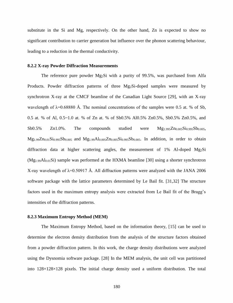
180
substitute in the Si and Mg, respectively. On the other hand, Zn is expected to show no
significant contribution to carrier generation but influence over the phonon scattering behaviour,
leading to a reduction in the thermal conductivity.
8.2.2 X-ray Powder Diffraction Measurements
The reference pure powder Mg2Si with a purity of 99.5%, was purchased from Alfa
Products. Powder diffraction patterns of three Mg2Si-doped samples were measured by
synchrotron X-ray at the CMCF beamline of the Canadian Light Source [29], with an X-ray
wavelength of λ=0.68880 Å. The nominal concentrations of the samples were 0.5 at. % of Sb,
0.5 at. % of Al, 0.5~1.0 at. % of Zn at. % of Sb0.5% Al0.5% Zn0.5%, Sb0.5% Zn0.5%, and
Sb0.5% Zn1.0%. The compounds studied were Mg1.995Zn0.005Si0.995Sb0.005,
Mg1.99Zn0.01Si0.995Sb0.005 and Mg1.99Al0.005Zn0.005Si0.995Sb0.005. In addition, in order to obtain
diffraction data at higher scattering angles, the measurement of 1% Al-doped Mg2Si
(Mg1.99Al0.01Si) sample was performed at the HXMA beamline [30] using a shorter synchrotron
X-ray wavelength of λ=0.50917 Å. All diffraction patterns were analyzed with the JANA 2006
software package with the lattice parameters determined by Le Bail fit. [31,32] The structure
factors used in the maximum entropy analysis were extracted from Le Bail fit of the Bragg’s
intensities of the diffraction patterns.
8.2.3 Maximum Entropy Method (MEM)
The Maximum Entropy Method, based on the information theory, [15] can be used to
determine the electron density distribution from the analysis of the structure factors obtained
from a powder diffraction pattern. In this work, the charge density distributions were analyzed
using the Dysnomia software package. [28] In the MEM analysis, the unit cell was partitioned
into 128×128×128 pixels. The initial charge density used a uniform distribution. The total

181
scattering factor (F(000)) was scaled to the nominal concentration of the dopants. Thus, the
F(000)/a3 are 152 e/Å3 for pure Mg2Si, 153.1 e/Å3 for Mg1.995Zn0.005Si0.995Sb0.005, 153.46 e/Å3 for
Mg1.99Zn0.01Si0.995Sb0.005, 153.12 e/Å3 for Mg1.99Al0.005Zn0.005Si0.995Sb0.005, and 152.04 e/Å3 for
Mg1.99Al0.01Si. The three-dimensional (3D) and two-dimensional (2D) visualization charge
densities were plotted using the VESTA program. [33-36]
8.2.4 Electronic Structure Calculations
First principles electronic calculations were performed using density functional theory
(DFT) within the Perdew-Burke Ernzerhof (PBE) parameterization of the generalized gradient
approximation (GGA) as implemented in the Vienna ab initio simulation package (VASP) code.
[37-40] For all calculations, the projector-augmented wave (PAW) [41,42] potentials were used
with the following valence configurations: 3s23p1 for Al, 3d104s2 for Zn, 5s25p3 for Sb, 3s23p0 for
Mg and 3s23p2 for Si.
For Al, Zn, and Sb substitutions, two models with different substitution sites were
considered. Two models with 0.6% at Al Zn Sb doped Mg2Si were constructed from a 3×3×3
supercell of the pure crystal. In the first, Zn atoms were put on the Mg sites with Si sites
substituted by Al and Sb (i.e. (Mg214Zn2)(Si104Al2Sb2)). In the second model, some Mg atoms
were replaced by Al and Zn with Si sites substituted by Sb (i.e. (Mg212Zn2Al2)(Si106Sb2)). A
2×2×2 k-point mesh was used for the calculation of the projected density of states (pdos) on the
supercells.
8.3 Results and Discussion
High-resolution synchrotron angle dispersive X-ray diffraction patterns of pure Mg2Si
and doped Mg2Si samples were measured under ambient conditions (Fig. 8.1 (a) and (b)). The
lattice parameters were determined from full profile Le Bail to the diffraction patterns using

182
angular data with range from 5º to 40º. The X-ray diffraction patterns of pure Mg2Si can be
indexed readily to the cubic anti-fluorite (CaF2) structure with space group Fm-3m. In increasing
diffraction angle, the Miller indices (hkl) of the Bragg peaks were assigned to (111), (200), (220),
(311), (222), (400), (331), (420), (422), (511), (440), (531) and (600) reflections. The diffraction
patterns of all the multi-doped Mg2Si samples share the same profile as pure Mg2Si except the
positions of the Bragg peaks shifted noticeably to lower angles. (See Fig. 8.1 (a)) This indicates
that even with small dopant concentrations (0.5%~1.0%) the cubic lattice of Mg2Si was
expanded. This is clearly seen in the expanded region 9º-12º of the (111) peak. (See Fig. 8.1 (b))
The cubic cell parameter of pure Mg2Si a = 6.2843(9) Å is increased to 6.3571(9) Å to 6.3634(9)
Å by the substitutions of the dopants Zn, Al, and Sb, respectively. This trend can be rationalized
from the fact that the atomic sizes of Zn and Al dopants that are larger than Mg, and Sb is larger
than Si. A more detailed examination of the lattice constants of the doped Mg2Si samples shows,
for instance, compared with Mg1.995Zn0.005Si0.995Sb0.005, the lattice constant of
Mg1.99Zn0.01Si0.995Sb0.005 is larger, possibly due to the higher doping concentration of Zn. In
comparison, the lattice parameter of Mg1.995Zn0.005Si0.995Sb0.005 is similar to
Mg1.99Al0.005Zn0.005Si0.995Sb0.005, suggesting that Al has a weaker effect on the expansion of the
crystal lattice, probably due to the similar atomic sizes of Al and Mg atoms.
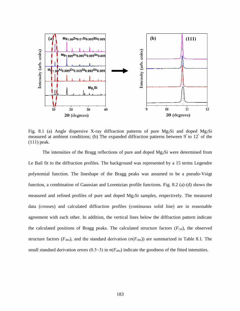
183
Fig. 8.1 (a) Angle dispersive X-ray diffraction patterns of pure Mg2Si and doped Mg2Si
measured at ambient conditions; (b) The expanded diffraction patterns between 9º to 12º of the
(111) peak.
The intensities of the Bragg reflections of pure and doped Mg2Si were determined from
Le Bail fit to the diffraction profiles. The background was represented by a 15 terms Legendre
polynomial function. The lineshape of the Bragg peaks was assumed to be a pseudo-Voigt
function, a combination of Gaussian and Lorentzian profile functions. Fig. 8.2 (a)-(d) shows the
measured and refined profiles of pure and doped Mg2Si samples, respectively. The measured
data (crosses) and calculated diffraction profiles (continuous solid line) are in reasonable
agreement with each other. In addition, the vertical lines below the diffraction pattern indicate
the calculated positions of Bragg peaks. The calculated structure factors (Fcal), the observed
structure factors (Fobs), and the standard derivation (σ(Fobs)) are summarized in Table 8.1. The
small standard derivation errors (0.5~3) in σ(Fobs) indicate the goodness of the fitted intensities.
(a) (b) (111)

184
Fig. 8.2 Le Bail fit to the experimental X-ray diffraction patterns for (a) pure Mg2Si; (b)
Mg1.99Al0.005Zn0.005Si0.995Sb0.005; (c) Mg1.995Zn0.005Si0.995Sb0.005; and (d) Mg1.99Zn0.01Si0.995Sb0.005.
Rp = 5.21%
Rwp
= 9.6%
Rp = 1.58%
Rwp= 2.08%
(a)
(d)
(b)
Rp = 2.34%
Rwp= 2.54%
Rp = 2.32%
Rwp= 2.83%
(c)
Rp = 3.15%
Rwp= 3.17%

185
Table 8.1 The structure factor of pure & doped Mg2Si obtained from diffraction data.
Mg1.99Al0.005Zn0.005Si0.995Sb0.005
h k l Fobs Fcal σ (Fobs)
1 1 1 47.17 46.60 0.91
0 0 2 -26.05 -25.90 0.86
2 0 2 100.00 97.78 1.54
1 1 3 33.00 32.93 0.95
2 2 2 -23.39 -23.22 0.57
0 0 4 82.94 80.94 2.33
3 1 3 31.17 29.96 1.30
2 0 4 -18.40 -18.09 0.58
2 2 4 72.62 70.10 1.49
3 3 3 27.33 26.61 1.41
1 1 5 27.33 25.79 1.41
4 0 4 66.94 61.73 2.40
3 1 5 24.39 22.93 1.37
0 0 6 -10.54 -10.63 1.18
4 2 4 -10.54 -10.81 1.18
Pure Mg2Si
h k l Fobs Fcal σ (Fobs)
1 1 1 45.61 44.07 0.71
0 0 2 -31.15 -31.51 0.84
2 0 2 100.00 100.08 1.23
1 1 3 33.97 35.51 0.70
2 2 2 -26.81 -26.40 0.90
0 0 4 87.36 87.49 1.71
3 1 3 30.76 31.48 0.90
2 0 4 -21.82 -20.91 0.97
2 2 4 75.60 74.42 1.16
3 3 3 27.17 27.26 0.83
1 1 5 27.17 27.45 0.83
4 0 4 68.14 65.73 1.64
3 1 5 24.68 24.48 0.52
0 0 6 -13.43 -13.43 0.27
4 2 4 -13.43 -13.49 0.27

186
Mg1.995Zn0.005Si0.995Sb0.005
h k l Fobs Fcal σ (Fobs)
1 1 1 47.67 46.72 1.09
0 0 2 -28.16 -27.68 1.13
2 0 2 100.00 98.33 1.66
1 1 3 34.64 32.81 1.22
2 2 2 -23.64 -23.16 0.95
0 0 4 89.51 84.99 2.99
3 1 3 31.83 29.64 1.73
2 0 4 -18.82 -18.46 0.61
2 2 4 74.72 71.38 1.87
3 3 3 28.06 27.64 0.98
1 1 5 28.06 26.97 0.98
4 0 4 65.40 61.09 3.27
3 1 5 25.36 22.82 1.88
0 0 6 -11.36 -11.26 1.13
4 2 4 -11.36 -11.37 1.13
Mg1.99Zn0.01Si0.995Sb0.005
h k l Fobs Fcal σ (Fobs)
1 1 1 47.60 46.69 0.88
0 0 2 -29.02 -28.59 0.81
2 0 2 100.00 100.08 1.40
1 1 3 36.67 35.10 0.89
2 2 2 -24.64 -23.90 0.91
0 0 4 90.71 88.22 2.18
3 1 3 31.36 30.01 0.98
2 0 4 -19.86 -19.25 0.57
2 2 4 74.47 73.19 1.42
3 3 3 28.57 27.92 1.23
1 1 5 28.57 27.03 1.23
4 0 4 64.88 63.22 2.16
3 1 5 25.49 23.76 1.16
0 0 6 -11.52 -11.56 1.12
4 2 4 -11.52 -11.63 1.12
187
The charge densities of the samples were determined from the structure factors extracted
from the X-ray diffraction patterns using the MEM. For pure Mg2Si, convergence in the MEM
refinement was reached when the Lagrange parameter (λ)=0.001 and reliability indices
RMEM=1.58% and wRMEM=2.08% were achieved (where RMEM is the unweighted index and
wRMEM is the weighted index). For the doped Mg2Si samples, similar analyses with comparable
accuracy were obtained. The 3D MEM charge density surface contour plot for pure Mg2Si
showed the correct positions of charge density in Mg and Si sites (Fig. 8.3) in the unit cell.
Electron densities are concentrated at the equivalent 4a sites of Si (0,0,0) and the 8c (1/4,1/4,1/4)
sites of Mg. This picture is consistent with the face-centered cubic crystal structure of pure
Mg2Si with an Fm-3m space group. Furthermore, visualization of the charge density shows the
ionic of the chemical bonding indicating the electron charges distribution are visually very
similar at the Si and Mg sites as the size of the charge clouds were comparable between the Mg
and Si atoms. The results obtained here are similar to those previously reported. [22]

188
Fig. 8.3 3D charge density of pure Mg2Si in the unit cell (The value of the contour surface is 0.5
e/Å3.)
To reveal the distribution of the excess electrons donated by the dopants, three-
dimensional (3D) and two-dimensional (2D) electron densities difference (Δρ) maps in which the
electron density of pure Mg2Si was subtracted from the doped samples were calculated. The 3D
electron distribution differences are shown in Fig. 8.4 (a) and (b). In Fig. 8.4 (a) and (b), positive
and negative differences were plotted with surface contours of ±0.5 e/Å3, respectively. It is
surprising that both positive and negative density difference were found in the atomic core
regions. It might suggest there may be core polarization. However, as will be discussed below,
this explanation is untenable as the inherent errors in the analysis are very large in the atomic
core region.
A strategy to analyze the MEM results is to fix the unit cells of the doped Mg2Si samples
to that of pure Mg2Si. In this case, for the doped Mg2Si samples, the only difference is the
number of electrons added in the unit cell. As mentioned above, we always found spurious
positive and negative electron density (-0.5~0 e/Å3) inside the core region of Mg atoms. This
Si (0 0 0)
Mg (¼ ¼ ¼)

189
observation is unrealistic as we have only used X-ray diffraction data up to a d-spacing of 1 Å,
therefore, it is not expected that reliable density with r<1 Å can be obtained. We therefore
ignored the core electron density and only analyzed the positive electron density difference. In
Fig. 8.5, the electron density difference maps of the doped samples projected in the (100) and
(110) planes of the unit cell are compared by using the experimental unit cells for the analysis of
the MEM for the doped samples. The (100) plane contains only the Si atoms and the (110) plane
contains both Si and Mg atoms. The results show the obvious trend that all the doped samples
gained electrons in the crystal with the addition of the dopants (Sb, Al and Zn). The most
important observation is that, even though doped atoms are expected to locate at specific atom
sites, the extra electrons are not localized in specific spatial regions, but both Mg and Si sites
gain electrons. This observation will be explained later with the DFT-calculated density of states.
Examination of the MEM derived electron densities of the doped Mg2Si samples shows
the charge accumulation on the Si sites increased in the order of Mg1.99Al0.005Zn0.005Si0.995Sb0.005
(Sb0.5%Al0.5%Zn0.5%)<Mg1.995Zn0.005Si0.995Sb0.005 (Sb0.5%Zn0.5%)<Mg1.99Zn0.01Si0.995Sb0.005
(Sb0.5%Zn1.0%). (See Fig. 8.5(a) and (b)) Comparing the charge density difference maps
containing only the Si atoms in the (100) plane (Fig. 8.5 (a)), we found that
Mg1.995Zn0.005Si0.995Sb0.005 and Mg1.99Zn0.01Si0.995Sb0.005 are similar, indicating that the increase of
Zn concentration does not affect the charge distribution, so it is likely that Zn does not occupy
the Si sites. The charge density difference of Mg1.99Al0.005Zn0.005Si0.995Sb0.005 is different from
those of Mg1.995Zn0.005Si0.995Sb0.005 and Mg1.99Zn0.01Si0.995Sb0.005. Since the only difference in
chemistry is the addition of the Al atom in Mg1.99Al0.005Zn0.005Si0.995Sb0.005, we may conclude Al
occupies the Si sites. An additional evidence is that the charge density on the Si sites in
Mg1.99Al0.005Zn0.005Si0.995Sb0.005 is lower than the other two compounds
190
(Mg1.995Zn0.005Si0.995Sb0.005 and Mg1.99Zn0.01Si0.995Sb0.005), since Al has one less electron that Si. If
the Zn atoms indeed is situated at the Mg sites, as suggested above one would expect when the
concentration of Zn is increased from 0.5% to 1.0%, there will be more electrons at the sites.
This description is indeed confirmed by the difference in electron topology around the Mg sites
showing an increase of electron density from 0.5% to 1.0% Zn. Finally, unlike Si sites, the
electrons distribution around Mg sites is not spherical, but show additional features. The
apparent difference can be explained by the fact the both Mg and Si atoms are sp3 hybridized.
The Mg atoms are tetrahedrally arrayed around Si and vice versa. However, in the (100) plane
showing the Si atoms, there is no projection of the electron density of the Si-Mg bond on this
plane. On the other hand, the (110) plane cuts into the Mg-Si sp3 hybrid orbitals and therefore
resulting in the addition feature. Therefore, from the MEM charge density analysis, we can
conclude that the Zn dopants should occupy the Mg sites. The increase in electron density
suggests both Al and Sb occupied the Si sites. This suggestion is at odd with the n-type
semiconductor property of the synthesized samples, which indicate Al dopants substitute the Mg
and the extra electrons are in the valence band. However, a recent theoretical calculation
suggested that the conclusion on the Al substitution site in Mg2Si is still ambiguous, in particular
at low Al concentration. [14] The present results provide a new perspective on the possible
locations of the dopants in the crystal: Al and Sb substituted the Si sites but only Zn occupied the
Mg sites.
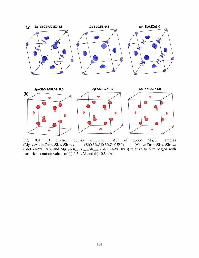
191
Fig. 8.4 3D electron density difference (Δρ) of doped Mg2Si samples
(Mg1.99Al0.005Zn0.005Si0.995Sb0.005 (Sb0.5%Al0.5%Zn0.5%), Mg1.995Zn0.005Si0.995Sb0.005
(Sb0.5%Zn0.5%), and Mg1.99Zn0.01Si0.995Sb0.005 (Sb0.5%Zn1.0%)) relative to pure Mg2Si with
isosurface contour values of (a) 0.5 e/Å3 and (b) -0.5 e/Å3.
(a)
(b)

192
Fig. 8.5 2D electron density difference (Δρ) of doped Mg2Si samples
(Mg1.99Al0.005Zn0.005Si0.995Sb0.005 (Sb0.5%Al0.5%Zn0.5%), Mg1.995Zn0.005Si0.995Sb0.005
(Sb0.5%Zn0.5%), and Mg1.99Zn0.01Si0.995Sb0.005 (Sb0.5%Zn1.0%)) relative to pure Mg2Si in (a)
(100) and (b) (110) planes. The contour levels are shown in the side bars.
Since the exact locations of the dopants are not certain, we performed theoretical DFT
calculations on two different multi-doped Mg2Si models in order to clarify the situation. In the
first model, we assumed that the Zn atoms substituted the Mg sites, and Al and Sb resided at the
Si sites. (i.e. (Mg214Zn2)(Si104Al2Sb2)). In the second model, Mg atoms were replaced with Al
and Zn and Si atoms were replaced with Sb (i.e. (Mg212Zn2Al2)(Si106Sb2)). In Fig. 8.6 (a) and (b),
we observed no localized mid gap band and the electrons are delocalized over the entire crystal
structure. It should be noted that both structural models resulted in an n-type semiconductor. (Fig.
8.6 (a)) The first model shows below and at the Fermi level the dominant contributions are from
Si, Mg and Al atoms with very small participation of Zn and Sb atoms. In Fig. 8.6 (b), the
(a)
(b)
193
density of states is projected into individual atomic orbitals. The p-type atomic orbitals of both
Mg and Si atoms contribute to the density of states near the Fermi level is clear and supporting
the suggestion that both Mg and Si are sp3 hybridized.
The calculated projected densities of states (pdos) of the second multi-doped
(Mg212Zn2Al2)(Si106Sb2) model are shown in Fig. 8.7 (a) and (b). The only difference of this
model with the previous one is that Al atoms now substituted the Mg sites instead of the Si. If
this was the case, there will be more free electrons available with this substitution. Comparing to
the (Mg214Zn2)(Si104Al2Sb2) model, the Fermi level indeed shifts to a higher energy as more free
electrons should contribute to the conduction band. The same observation is made that the
calculated projected orbital densities of states for all atoms show that, although the dopants
replace the Mg and Si sites, the dopant electrons are spread over the entire crystal and not
localized in specific regions.
To conclude, the electronic structures of two theoretical structural models, i.e with Al
substituting either the Mg or Si sites, cannot differentiate the preference sites of the dopants.
However, the results also do not contradict the observed electron density difference discussed
above, indirectly showing the present assignments of the substitution sites are plausible.
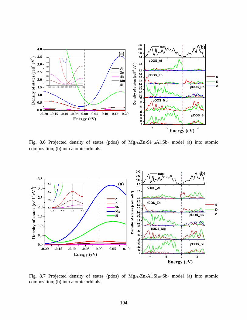
194
Fig. 8.6 Projected density of states (pdos) of Mg214Zn2Si104Al2Sb2 model (a) into atomic
composition; (b) into atomic orbitals.
Fig. 8.7 Projected density of states (pdos) of Mg212Zn2Al2Si106Sb2 model (a) into atomic
composition; (b) into atomic orbitals.
-0.20 -0.15 -0.10 -0.05 0.00 0.05 0.10 0.15 0.200.0
0.5
1.0
1.5
2.0
2.5
3.0
3.5
4.0
Den
sity
of
stat
es (
cell
-1 e
V-1)
Energy (eV)
Al
Zn
Sb
Mg
Si
0
100
200
300
0.0
0.5
1.0
0.0
0.5
1.0
1.5
2.0
0.00.20.40.60.81.0
0
10
20
30
-4 -2 0 2
0
10
20
30
40
Den
sit
y o
f sta
tes
(ce
ll-1 e
V-1)
total
pDOS_Al
pDOS_Si
pDOS_Mg
pDOS_Sb
pDOS_Zn s
p
d
-0.20 -0.15 -0.10 -0.05 0.00 0.05 0.10 0.15 0.200.00
0.05
0.10
0.15
0.20
0.25
0.30
(a)
(b)
(b)
(a)
Energy (eV)
Energy (eV)

195
The maximum entropy method (MEM) is a powerful technique to determine the electron
density distribution if only a limited set of diffraction data is available. However, it does have
limitations. First, the quality of the experimental data is an important factor, this is particularly
important for the intensities extracted from powder patterns. Second, the calculated electron
density is dependent on the numbers of Bragg reflections considered in the MEM analysis (i.e.
errors introduced by the limited maximum scattering angle). We investigated this effect on a 1%
Al-doped Mg2Si sample (Mg1.99Al0.01Si) using synchrotron radiation measured with a shorter
wavelength (λ=0.50917 Å), in which higher angle Bragg reflections were collected. From 5 º to
52º, a total of 55 non-overlapping reflections can be indexed and their intensities extracted (Fig.
8.8). To study the errors introduced to the computed charge density due to the restricted number
of reflections included in the calculations, MEM charge density maps were constructed with 15,
20, 30, 45 and 55 Bragg reflections. Deviations of the charge density were examined from the
difference with the full data set (i.e. 55 reflections). As shown in Fig. 8.9, the major discrepancy
is concentrated at the atomic sites with a radial spread of ca. ~1 Å. This is not surprising as the
high angle structure factors are more sensitive to the core electrons. In the worst possible case
(i.e. using 15 Bragg reflections) the largest difference in the electron density is at most 14 e/Å3
with a spread of the electron density about 1 Å. Since the positive electron density differences
are located away from the atomic sites in the density maps of the doped samples, we believe the
results are qualitatively correct. Although the errors of electron density in the core regions
become smaller as an increasing number of Bragg reflections are introduced, we conclude that it
is difficult to obtain highly accurate measurements of the electron density distribution for the
doped samples with small doping concentrations by using the MEM.

196
Fig. 8.8 Refined X-ray diffraction pattern for 1% Al-doped Mg2Si (Mg1.99Al0.01Si).
Fig. 8.9 3D electron density difference of 1% Al-doped Mg2Si (Mg1.99Al0.01Si) (a) between 15
and 55 reflection peaks used; (b) between 20 and 55 reflection peaks used; (c) between 30 and 55
reflection peaks used; and (d) between 45 and 55 reflection peaks used. (Yellow: positive charge
density; Green: negative charge density)
(a)
10 20 30 40 50
Inte
nsi
ty (
arb
. u
nit
s)
2degrees)
Observation
Calculation
Difference
Rp = 5.49%
Rwp= 5.51%
(b) (c) (d)

197
8.4 Conclusion
High resolution powder diffraction patterns of pure and multi-doped Mg2Si have been
measured by synchrotron X-ray. Analyses show the addition of the dopants expanded the unit
cells from pure Mg2Si. It is gratifying that even using a limited set of low angle Bragg reflections
the charge density distribution of pure Mg2Si can be reconstructed using the Maximum Entropy
Method (MEM). Analysis also revealed subtle differences in the valence electron topologies
between doped and pure samples. It is found that the electrons contributed by the dopants
populated the conduction band and are not localized on the dopant sites. This observation is
supported by results of theoretical DFT calculations on two different doping models showing
that these electrons occupied the conduction bands and are delocalized. In contrast to the electron
density difference profile in (100) plane showing only the Si atoms, in the (110) plane, the
electrons distribution around Mg sites is found to have additional features. These features can be
explained by electrons on the Mg polarized along the Mg-Si bond direction in the (110) plane but
have no projection in the (100) plane. Studies on the charge density difference maps strongly
suggest that the Zn dopant should occupy the Mg sites whilst Al and Sb occupied the Si sites.
Comparisons of MEM charge densities calculated with systematic increase in the number of high
angle Bragg reflections included in the analysis on Al-doped Mg2Si indicate that the electron
density maps for the multi-doped samples are denominated by the valence electrons and should
be qualitatively correct.
Acknowledgments
Synchrotron X-ray diffraction experiments were performed at the CMCF and HXMA
beamlines of the Canadian Light Source, which were made possible by support from NSERC,
NRC, CIHR, and the University of Saskatchewan. The sample preparation was partly supported

198
by a Grant-in-Aid for Research (A) by the Japanese Ministry of Education, Science, Sports, and
Culture. JZ and JST thank AUTO21 for a research grant.
References
[1] T. Sakamoto, T. Iida, S. Kurosaki, K. Yano, H. Taguchi, K. Nishio, and Y. Takanashi,
Journal of Electronic Materials, 2011, 40, 629-634.
[2] S. Battiston, S. Fiameni, M. Saleemi, S. Boldrini, A. Famengo, F. Agresti, M. Stingaciu,
M. S. Toprak, M. Fabrizio, and S. Barison, Journal of Electronic Materials, 2013, 42,
1956-1959.
[3] T. Sakamoto, T. Iida, A. Matsumoto, Y. Honda, T. Nemoto, J. Sato, T. Nakajima, H.
Taguchi, and Y. Takanashi, Journal of Electronic Materials, 2010, 39, 1708-1713.
[4] S. You, K. Park, I. Kim, S. Choi, W. Seo, and S. Kim, Journal of Electronic Materials,
2011, 41, 1675-1679.
[5] J. Tani and H. Kido, Intermetallics, 2008, 16, 418-423.
[6] N. Wang, H. Chen, H. He, W. Norimatsu, M. Kusunoki, and K. Koumoto, Scientific
Reports, 2013, 3, 3449.
[7] Q. Chen, Q. Xie, F. Zhao, D. Cui, and X. Li, IEEE Computer Society, 2009, 22, 338-341.
[8] G. J. Snyder and E. S. Toberer, Nature Materials, 2008, 7, 105-114.
[9] G. H. Kim, L. Shao, K. Zhang, and K. P. Pipe, Nature Materials, 2013, 12, 719-723.
[10] M. Christensen, N. Lock, J. Overgaard, and B. B. Iversen, J. Am. Chem. Soc., 2006, 128,
15657.
[11] J. Zhao, Z. Liu, J. Reid, K. Takarabe, T. Iida, B. Wang, U. Yoshiya, and J. S. Tse, Journal
of Materials Chemistry A, 2015, 3, 19774-19782.
[12] N. Farahi, M. VanZant, J. Zhao, J. S. Tse, S. Prabhudev, G. A. Botton, J. R. Salvador, F.
Borondics, Z. Liu, and H. Kleinke, Dalton Transactions, 2014, 43, 14983-14991.
[13] J. Zhao, Z. Liu, R. A. Gordon, K. Takarabe, J. Reid, and J. S. Tse, Journal of Applied
Physics, 2015, 118, 145902.
[14] P. Zwolenski, J. Tobola, and S. Kaprzyk, Journal of Electronic Materials, 2011, 40, 889-
897.
[15] D. M. Collins, Nature, 1982, 298, 49-51.
199
[16] N. K. Hansen and P. Coppens, Acta. Cryst., 1978, A34, 909-921.
[17] S. V. Smaalen and J. Netzel, Phys. Scr., 2009, 79, 048304.
[18] R. Saravanan and M. P. Rani, Metal and Alloy Bonding- An Experimental Analysis,
Springer-Verlag London Press, 2012.
[19] K. S. S. Ali, R. Saravanan, A. V. Pashchenko, and V. P. Pashchenko, Journal of Alloys
and Compounds, 2010, 501, 307-312.
[20] S. Francis, R. Saravanan, and L. J. Berchmans, Journal of Electronic Materials, 2013, 42,
701.
[21] Y. Takahashi, Y. Gotoh, and J. Akimoto, Journal of Solid State Chemistry, 2003, 172, 22-
26.
[22] R. Saravanan and M. C. Robert, Journal of Alloys and Compounds, 2009, 479, 26-31.
[23] R. Saravanan and M. C. Robert, Journal of Physics and Chemistry of Solids, 2009, 70,
159-163.
[24] R. Saravanan, Phys. Scr., 2009, 79, 048303.
[25] F. Gargnoni, E. Nishibori, P. Rabiller, L. Bertini, G. J. Snyder, M. Christensen, C. Gatti,
and B. B. Iversen, Chem. Eur. J., 2004, 10, 3861-3870.
[26] A. Ohno, S. Sasaki, E. Nishibori, S. Aoyagi, M. Sakata, and B. B. Iverson, Physical
Review B, 2007, 76, 064119.
[27] S. Kastbjerg, N. Bindzus, M. SØndergaard, S. Johnsen, N. Lock, M. Christensen, M.
Takata, M. A. Spackman, and B. B. Iversen, Advanced Functional Materials, 2013, 23,
5477-5483.
[28] K. Momma, T. Ikeda, A. A. Belik and F. Izumi, Powder Diffraction, 2013, 28, 184-193.
[29] http://cmcf.lightsource.ca/beamlines/08b1-1/
[30] T. D. Jiang, N. Chen, and W. Sheng, Wiggler-based Hard X-ray spectroscopy beamline at
CLS, AIP Proc. (Accelerators and Beams), 2009, 879, 800-803.
[31] V. Petricek, M. Dusek, and L. Palatinus, Z. Kristallogr., 2014, 229, 345-352.
[32] A. Le Bail, H. Duroy, and J. L. Fourquet, Materials Research Bulletin, 1988, 23, 447-452.
[33] F. Izumi and K. Momma, Proc. XX Conf. Appl. Crystallogr., Solid State Phenom., 2007,
130, 15-20.
200
[34] K. Momma and F. Izumi, Commission on Crystallogr. Comput., IUCr Newslett., 2006, 7,
106-119.
[35] K. Momma and F. Izumi, J. Appl. Crystallogr., 2008, 41, 653-658.
[36] K. Momma and F. Izumi, J. Appl. Crystallogr., 2011, 44, 1272-1276.
[37] G. Kresse and J. Hafner, Physical Review B, 1993, 47, 558.
[38] G. Kresse and J. Hafner, Physical Review B, 1994, 49, 14251.
[39] G. Kresse and J. Furthmller, Computational Materials Science, 1996, 6, 15.
[40] G. Kresse and J. Furthmller, Physical Review B, 1996, 54, 11169.
[41] P. E. Blöchl, Physical Review B, 1994, 50, 17953.
[42] G. Kresse and D. Joubert, Physical Review B, 1999, 59, 1758.
201
CHAPTER 9
SUMMARY AND PERSPECTIVES
The research reported in this thesis has fulfilled its initial objectives: to characterize the
electronic, electrical, and structural properties of doped Mg2Si thermoelectric materials using
state-of-the-art synchrotron radiation techniques (infrared reflectivity/absorption spectra and
powder X-ray diffraction) and theoretical density functional (DFT) calculations. However, there
are still opportunities for improvements and future investigation. In this chapter, the major
results and contributions are summarized, and opportunities for future work are presented.
9.1 Summary
We studied Mg2Si doped with a variety of elements and obtained the samples’ transport
properties using infrared reflectivity measurements. DFT calculations were performed to explain
the electronic structures and electrical properties. We demonstrated that the Seebeck coefficients
of doped Mg2Si samples can be reproduced by the rigid band approximation using the
Boltzmann transport theory. We found the thermoelectric performances of samples single-doped
with Sb and Bi could indeed be enhanced with electron donating dopants. We further replaced Si
in Bi-doped Mg2Si with heavier Ge atoms in order to decrease the lattice thermal conductivity.
From the analysis of IR reflectivity data, a significant decrease in the electrical conductivity was
found with increasing Ge content. However, Ge helped to reduce the lattice thermal conductivity.
As a result, the overall effect was the enhancement of the thermoelectric figure of merit.
Doping was found to affect the crystal structure of Mg2Si. Angle-dispersive synchrotron
radiation X-ray powder diffraction provided structural information on Sb, Al, and Zn multi-
doped Mg2Si powder samples, synthesized by spark plasma sintering. Small concentrations of
the dopants (0.5-1.0%) did not alter the overall cubic crystal symmetry of the host lattice but

202
expanded the unit cell sizes noticeably by 1.1%-1.2%. Electrical transport properties were
characterized by mid-IR reflectivity and compared to bulk quasi-four probe measurements. The
infrared reflectivities show the doped samples were semiconductors at room temperature. The
trend in the dc conductivities derived from the analysis of the infrared reflectivity spectra
employing the Drude-Lorentz model is in qualitative agreement with the conventional bulk
measurements. However, the absolute values obtained from IR reflectivities were found to be
consistently lower. We attribute the discrepancy to non-uniform distributions of the doped atoms
in the sample. The carrier electron concentrations (N) can be determined from Hall coefficients
obtained from the bulk measurements, and the plasma frequencies (ωp) can be obtained from the
infrared reflectivity spectra. From the values of N and ωp, the electron effective masses were
found to be between 0.255me and 0.361me. The lighter effective masses reflect a higher electrical
conductivity in the doped Mg2Si. A best thermoelectric performance figure of merit (ZT) of
0.964 was achieved for the Mg1.995Zn0.005Si0.995Sb0.005 at 880 K, very close to the ZT of PbTe that
is the present choice in many commercial products.
We investigated the mechanism for the observed enhancement of thermal power of Al-
doped Mg2Si under pressure. The structures of a nominally 1 at. % Al-doped Mg2Si sample
(Mg1.99Al0.01Si) were measured by angle dispersive synchrotron radiation X-ray diffraction and
the electrical conductivity by infrared reflectivity. All measurements were performed at room
temperature up to 16.6 GPa. Contrary to previous reports, no structural transformation was
observed in pure Mg2Si up to 15 GPa when helium was used here as the pressure transmission
medium. This is substantiated by the electronic band structures of pure Mg2Si with density
functional theory including the correction for the electron correlation effect with the GW
approximation showing the band gap of Mg2Si does not close at 11 GPa. The theoretical

203
electronic density of states is consistent with electrical resistivity measurements showing that
Mg2Si did not transform to a metal at least up to 22 GPa. The present diffraction and theoretical
results contradict reports on the structural phase transition to metallic anti-cotunnite and Ni2In
structures at 7 and 11 GPa, respectively. In contrast, a structural phase transition from the cubic
anti-fluorite to the anti-cotunnite structure was found in Al-doped Mg2Si at 11.9 GPa. The dc
conductivities at high pressure calculated from the analysis of infrared reflectivity spectra
employing the Drude-Lorentz model were found to increase after the phase transition. The
results also show the Al-doped Mg2Si already exhibited semi-metallic-like behaviour under
ambient conditions. The results from synchrotron IR reflectivity agree with bulk four-probe
measurements, in which the electrical conductivity was found to increase with pressure. From
the theoretical density of electronic states, a maximum thermoelectric power factor was predicted
at 2-3 GPa, which is in good agreement with the experimental observation.
We investigated the possibility of mixing multi-wall carbon nanotubes (MWCNTs), a
good conductor, to enhance the electrical conductivity and, therefore, the thermoelectric
properties of Mg2Si0.877Ge0.1Bi0.023. Indeed, we found the addition of MWCNTs increased the
electrical conductivity. At 323 K, the measured electrical conductivity was increased from 450
Ω-1cm-1 (undoped Mg2Si0.877Ge0.1Bi0.023) to 500 Ω-1cm-1 (doped Mg2Si0.877Ge0.1Bi0.023-0.5 wt%
MWCNTs), an increase of about 10%. However, the positive effect diminished at higher
temperature where the conductivity dropped back to 470 Ω-1cm-1 at 773 K. To clarify whether
the enhancement was due to chemical interaction between the MWCNTs and
Mg2Si0.877Ge0.1Bi0.023, we performed Raman measurements on the samples. The persistence of
disorder (D) and tangential (G) vibrational mode characteristics of a carbon nanotube suggested
there was no decomposition or substantial chemical reaction of the MWCNTs doped in
204
Mg2Si0.877Ge0.1Bi0.023. The final result is that the best ZT of 0.5 obtained in Mg2Si0.877Ge0.1Bi0.023-
0.5 wt% MWCNTs at 700 K is not very attractive for practical applications.
The charge-densities of pure Mg2Si and multi-doped Mg2Si samples were constructed by
the Maximum Entropy Method (MEM) using synchrotron X-ray powder diffraction patterns. The
atomic positions were correctly located. We found the extra electrons contributed by the dopants
populated the conduction band but were not localized on the substituted dopant sites. This
observation is supported by results of theoretical DFT calculations showing there were no mid-
gap localized electron bands and the electrons were delocalized over the unit cell. In the (110)
plane of both the Mg and Si sites, the distribution of electrons around Mg sites was not spherical,
but showed additional features. The apparent difference can be explained by the fact that both
Mg and Si atoms were sp3 hybridized. The Mg atoms were tetrahedrally arranged around Si and
vice versa. However, in the (100) plane showing the Si atoms, there was no projection of the
electron density of the Si-Mg bond on this plane. On the other hand, the (110) plane cut into the
Mg-Si sp3 hybrid orbitals resulting in the additional feature. Therefore, from the MEM charge
density analysis, we can conclude that the Zn dopants should have occupied the Mg sites. The
increase in electron density suggests both Al and Sb occupied the Si sites. However, due to the
limited Bragg diffraction peaks measured, we conclude the effect of the dopants to the core
charge density cannot be reliably obtained from this data and only qualitative features of the
valence electron topology can be revealed. This conclusion is further confirmed from the
analysis of the diffraction pattern of an Al-doped Mg2Si (Mg1.99Al0.01Si) sample: The errors of
electron density in the core regions became smaller as the number of high angle Bragg
reflections included in the analysis was increased.

205
9.2 Perspectives
Several studies reported in this thesis can be further expanded and improved. As
discussed in Chapter 8, we found the error of the derived electron density in the atomic core
regions became smaller as the number of Bragg reflections included in the MEM analysis
increased. Despite many successes, MEM has its limitations in the quantitative determination of
the electron density distribution using just the low angle diffraction data. Another important
factor is the quality of the experimental data. This is particularly important for powder samples.
One way to further improve the accuracy of identifying electron density distribution using MEM
would be to re-visit these problems through the examination of single-crystal data. Using higher
angle X-ray single-crystal diffraction data, we might obtain more accurate results on electron
density distribution for the doped samples even with low doping concentrations.
We show the trends of the electrical conductivity obtained from IR reflectivity are similar
to the four-probe conductivity measurements of the bulk samples, however, the agreements on
the absolute magnitudes are not satisfactory. Since an infrared reflectivity measurement only
probes a very small spot of ca. 20 × 20 µm2 of the highly non-uniform doped sample, we
speculate that this is the main reason for the discrepancies. In further work, careful
characterization of the samples would be critical to resolve the discrepancy. It is possible to
measure IR reflectivities on different spots on the sample. Transmission electron microscopy
(TEM) would also complement the characterization of the locations of the dopants, particularly
around the grain boundaries.
In this research, the highest ZTmax≈1 was achieved in Mg1.995Zn0.005Si0.995Sb0.005 at 880K.
This value is still far from that needed for commercial applications. The thermoelectric samples
we studied were all in bulk form. However, low dimensional and nanocomposite thermoelectric
206
materials are known to dramatically enhance thermoelectric performance. [1-2] For example, ZT
was found to exceed 2 by using a 2D electron gas thin layer of SrTi0.8Nb0.2O3. [1] Previous
studies have also found 2D quantum-well, 1D quantum-wire of Bi2Te3 or PbTe-based
thermoelectric materials and bulk samples containing nanoparticles have the promising potential
to further increase thermoelectric performance. [3-7] For example, a nanostructural layer of
Bi2Te3 sample has been fabricated by electrochemical deposition from a solution. [8]
Investigations of thermoelectric performance of thin layer or nanostructural Mg2Si samples
would be interesting to undertake in the future. We expect that the effect of low dimensionality
and nanocomposites can significantly improve thermoelectric performance of doped Mg2Si-
based thermoelectric materials.
References
[1] H. Ohta, S. Kim, Y. Mune, T. Mizoguchi, K. Nomura, S. Ohta, T. Nomura, Y. Nakanishi,
Y. Ikuhara, M. Hirano, H. Hosono, and K. Koumoto, Nature Materials, 2007, 6, 129-134.
[2] L. D. Hicks and M. S. Dresselhaus, Physical Review B, 1993, 47, 12727.
[3] M. S. Dresselhaus, G. Chen, M. Y. Tang, R. Yang, H. Lee, D. Wang, Z. Ren, J. P. Fleurial,
and P. Gogna, Advanced Materials, 2007, 19, 1043-1053.
[4] R. R. Bourassa, D. Lazarus, and D. A. Blackburn, Physical Review, 1968, 165, 853.
[5] M. J. Yang, Q. Shen, and L. M. Zhang, China Phys. B, 2011, 20, 106202.
[6] M. J. Yang, W. J. Luo, and Q. Shen, Rare Met. Mater. Eng., 2009, S2, 1055-1059.
[7] S. Fiameni, S. Battiston, S. Boldrini, A. Famengo, F. Agresti, S. Barison, and M. Fabrizio,
Journal of Solid State Chemistry, 2012, 193, 142-146.
[8] S. Li, M. S. Toprak, H. M. A. Soliman, J. Zhou, M. Muhammed, D. Platzek, and E.
Müller, Chem. Mater., 2006, 18, 3627-3633.

207
APPENDIX A
Supplementary data for Chapter 3
Fig. A.1 Experimental powder diagrams of Mg2Si and Mg2Si0.98Bi0.02.
Fig. A.2 DSC and TG of Mg2Si0.98Bi0.02.
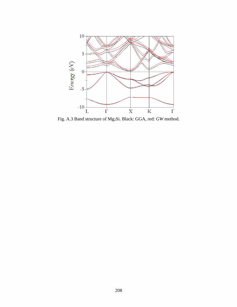
208
Fig. A.3 Band structure of Mg2Si. Black: GGA, red: GW method.

209
APPENDIX B
Supplementary data for Chapter 4
Fig. B.1 Experimental powder diagrams of Mg2Si0.977–xGexBi0.023 (0.1 ≤ x ≤ 0.4).
Fig. B.2 Specific heat of Mg2Si0.977–xGexBi0.023 (x = 0.1, 0.4).

210
Fig. B.3 Calculated Lorenz number of Mg2Si0.977–xGexBi0.023 (0.1 ≤ x ≤ 0.4).

211
APPENDIX C
Supplementary data for Chapter 7
Fig. C.1 Powder XRD patterns of Mg2Si0.877Ge0.1Bi0.023 samples.
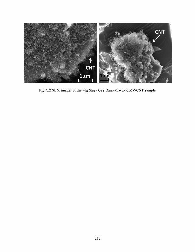
212
Fig. C.2 SEM images of the Mg2Si0.877Ge0.1Bi0.023/1 wt.-% MWCNT sample.
1μm
CNT
1μm
CNT

213
Fig. C.3 Low-magnification structural and compositional analyses of the edge of a grain.
EDXelemental mapping over a selected area showing the distribution of Mg, Si, Ge and Bi.
Fig. C.4 Medium temperature thermal conductivity of all samples with respect to MWCNT
content.

214
Fig. C.5 Lorenz number of all samples with regard to temperature.
Fig. C.6 Power factor of two bars obtained from 0.5% MWCNT/Mg2Si0.877Ge0.1Bi0.023
nanocomposite (6% error is considered).

215
Table C.1 Densities and specific heat of the Mg2Si0.877Ge0.1Bi0.023/MWCNT samples.
Sample Density
(gcm–3)
Relative density Cp
(Jg–1K–1)
Mg2Si0.877Ge0.1Bi0.023 2.10 96% 0.877
Mg2Si0.877Ge0.1Bi0.023 - 0.5 wt.-%
MWCNT
2.10 96% 0.882
Mg2Si0.877Ge0.1Bi0.023 - 1.0 wt.-%
MWCNT
2.04 93% 0.888
Mg2Si0.877Ge0.1Bi0.023 - 1.5 wt.-%
MWCNT
2.06 94% 0.894
Theoretical densities of the composite (𝑑C) were calculated using the mixture rule:
1
𝑑C=
wMWCNT
𝑑MWCNT+
wMatrix
𝑑Matrix
where dMWCNT, dMatrix, WMWCNT and WMatrix are the densities and mass fractions of the nanotubes
and Mg2Si0.877Ge0.1Bi0.023, respectively.

2016/1/5 Request Permission
http://pubs.rsc.org/en/content/requestpermission?msid=c4dt01177e 1/2
Sb- and Bi-doped Mg2Si: location of the
dopants, micro- and nanostructures,electronic structures and thermoelectricproperties
N. Farahi, M. VanZant, J. Zhao, J. S. Tse, S. Prabhudev, G. A. Botton, J. R.Salvador, F. Borondics, Z. Liu and H. Kleinke, Dalton Trans., 2014, 43, 14983DOI: 10.1039/C4DT01177E
If you are not the author of this article and you wish to reproduce material from itin a third party non-RSC publication you must formally request permission usingRightsLink. Go to our Instructions for using RightsLink page for details.
Authors contributing to RSC publications (journal articles, books or book chapters)do not need to formally request permission to reproduce material contained in thisarticle provided that the correct acknowledgement is given with the reproducedmaterial.
Reproduced material should be attributed as follows:
For reproduction of material from NJC: Reproduced from Ref. XX with permission from the Centre National de laRecherche Scientifique (CNRS) and The Royal Society of Chemistry.For reproduction of material from PCCP: Reproduced from Ref. XX with permission from the PCCP Owner Societies.For reproduction of material from PPS: Reproduced from Ref. XX with permission from the European Society forPhotobiology, the European Photochemistry Association, and The Royal Society ofChemistry.For reproduction of material from all other RSC journals and books: Reproduced from Ref. XX with permission from The Royal Society of Chemistry.
If the material has been adapted instead of reproduced from the original RSCpublication "Reproduced from" can be substituted with "Adapted from".
In all cases the Ref. XX is the XXth reference in the list of references.
If you are the author of this article you do not need to formally request permissionto reproduce figures, diagrams etc. contained in this article in third partypublications or in a thesis or dissertation provided that the correctacknowledgement is given with the reproduced material.
Reproduced material should be attributed as follows:

2016/1/5 Request Permission
http://pubs.rsc.org/en/content/requestpermission?msid=c4dt01177e 2/2
For reproduction of material from NJC: [Original citation] - Reproduced by permission of The Royal Society ofChemistry (RSC) on behalf of the Centre National de la Recherche Scientifique(CNRS) and the RSCFor reproduction of material from PCCP: [Original citation] - Reproduced by permission of the PCCP Owner SocietiesFor reproduction of material from PPS: [Original citation] - Reproduced by permission of The Royal Society ofChemistry (RSC) on behalf of the European Society for Photobiology, theEuropean Photochemistry Association, and RSCFor reproduction of material from all other RSC journals: [Original citation] - Reproduced by permission of The Royal Society ofChemistry
If you are the author of this article you still need to obtain permission toreproduce the whole article in a third party publication with the exception ofreproduction of the whole article in a thesis or dissertation.
Information about reproducing material from RSC articles with different licences isavailable on our Permission Requests page.

2016/1/5 RightsLink Printable License
https://s100.copyright.com/AppDispatchServlet 1/7
ELSEVIER LICENSETERMS AND CONDITIONS
Jan 05, 2016
This is a License Agreement between Jianbao Zhao ("You") and Elsevier("Elsevier") provided by Copyright Clearance Center ("CCC"). The licenseconsists of your order details, the terms and conditions provided byElsevier, and the payment terms and conditions.
All payments must be made in full to CCC. For payment instructions, please seeinformation listed at the bottom of this form.
Supplier Elsevier LimitedThe Boulevard,Langford LaneKidlington,Oxford,OX5 1GB,UK
Registered Company Number 1982084
Customer name Jianbao Zhao
Customer address #40330 Haight Crescent
Saskatoon, SK S7H4V9
License number 3782710615337
License date Jan 05, 2016
Licensed content publisher Elsevier
Licensed content publication Journal of Alloys and Compounds
Licensed content title Local structure and thermoelectric properties ofMg2Si0.977−xGexBi0.023 (0.1⩽x⩽0.4)
Licensed content author Nader Farahi,Sagar Prabhudev,Gianluigi A. Botton,Jianbao Zhao,JohnS. Tse,Zhenxian Liu,James R. Salvador,Holger Kleinke
Licensed content date 25 September 2015
Licensed content volumenumber
644
Licensed content issuenumber
n/a
Number of pages 7
Start Page 249
End Page 255
Type of Use reuse in a thesis/dissertation
Portion full article
Format electronic
Are you the author of thisElsevier article?
Yes
Will you be translating? No
Title of yourthesis/dissertation
STUDY OF Mg2SiBASED THERMOELECTRIC MATERIALS

2016/1/5 RightsLink Printable License
https://s100.copyright.com/AppDispatchServlet 2/7
Expected completion date Apr 2016
Estimated size (number ofpages)
202
Elsevier VAT number GB 494 6272 12
Permissions price 0.00 CAD
VAT/Local Sales Tax 0.00 CAD / 0.00 GBP
Total 0.00 CAD
Terms and Conditions
INTRODUCTION1. The publisher for this copyrighted material is Elsevier. By clicking"accept" in connection with completing this licensing transaction, youagree that the following terms and conditions apply to this transaction(along with the Billing and Payment terms and conditions established byCopyright Clearance Center, Inc. ("CCC"), at the time that you opened yourRightslink account and that are available at any time athttp://myaccount.copyright.com).
GENERAL TERMS2. Elsevier hereby grants you permission to reproduce the aforementionedmaterial subject to the terms and conditions indicated.3. Acknowledgement: If any part of the material to be used (for example,figures) has appeared in our publication with credit or acknowledgement toanother source, permission must also be sought from that source. If suchpermission is not obtained then that material may not be included in yourpublication/copies. Suitable acknowledgement to the source must be made,either as a footnote or in a reference list at the end of yourpublication, as follows:"Reprinted from Publication title, Vol /edition number, Author(s), Titleof article / title of chapter, Pages No., Copyright (Year), withpermission from Elsevier [OR APPLICABLE SOCIETY COPYRIGHT OWNER]." AlsoLancet special credit - "Reprinted from The Lancet, Vol. number,Author(s), Title of article, Pages No., Copyright (Year), with permissionfrom Elsevier."4. Reproduction of this material is confined to the purpose and/or mediafor which permission is hereby given.5. Altering/Modifying Material: Not Permitted. However figures andillustrations may be altered/adapted minimally to serve your work. Anyother abbreviations, additions, deletions and/or any other alterationsshall be made only with prior written authorization of Elsevier Ltd.(Please contact Elsevier at [email protected])6. If the permission fee for the requested use of our material is waivedin this instance, please be advised that your future requests for Elseviermaterials may attract a fee.7. Reservation of Rights: Publisher reserves all rights not specificallygranted in the combination of (i) the license details provided by you andaccepted in the course of this licensing transaction, (ii) these terms andconditions and (iii) CCC's Billing and Payment terms and conditions.8. License Contingent Upon Payment: While you may exercise the rightslicensed immediately upon issuance of the license at the end of the

2016/1/5 RightsLink Printable License
https://s100.copyright.com/AppDispatchServlet 3/7
licensing process for the transaction, provided that you have disclosedcomplete and accurate details of your proposed use, no license is finallyeffective unless and until full payment is received from you (either bypublisher or by CCC) as provided in CCC's Billing and Payment terms andconditions. If full payment is not received on a timely basis, then anylicense preliminarily granted shall be deemed automatically revoked andshall be void as if never granted. Further, in the event that you breachany of these terms and conditions or any of CCC's Billing and Paymentterms and conditions, the license is automatically revoked and shall bevoid as if never granted. Use of materials as described in a revokedlicense, as well as any use of the materials beyond the scope of anunrevoked license, may constitute copyright infringement and publisherreserves the right to take any and all action to protect its copyright inthe materials.9. Warranties: Publisher makes no representations or warranties withrespect to the licensed material.10. Indemnity: You hereby indemnify and agree to hold harmless publisherand CCC, and their respective officers, directors, employees and agents,from and against any and all claims arising out of your use of thelicensed material other than as specifically authorized pursuant to thislicense.11. No Transfer of License: This license is personal to you and may not besublicensed, assigned, or transferred by you to any other person withoutpublisher's written permission.12. No Amendment Except in Writing: This license may not be amended exceptin a writing signed by both parties (or, in the case of publisher, by CCCon publisher's behalf).13. Objection to Contrary Terms: Publisher hereby objects to any termscontained in any purchase order, acknowledgment, check endorsement orother writing prepared by you, which terms are inconsistent with theseterms and conditions or CCC's Billing and Payment terms and conditions. These terms and conditions, together with CCC's Billing and Payment termsand conditions (which are incorporated herein), comprise the entireagreement between you and publisher (and CCC) concerning this licensingtransaction. In the event of any conflict between your obligationsestablished by these terms and conditions and those established by CCC'sBilling and Payment terms and conditions, these terms and conditions shallcontrol.14. Revocation: Elsevier or Copyright Clearance Center may deny thepermissions described in this License at their sole discretion, for anyreason or no reason, with a full refund payable to you. Notice of suchdenial will be made using the contact information provided by you. Failure to receive such notice will not alter or invalidate the denial. In no event will Elsevier or Copyright Clearance Center be responsible orliable for any costs, expenses or damage incurred by you as a result of adenial of your permission request, other than a refund of the amount(s)paid by you to Elsevier and/or Copyright Clearance Center for deniedpermissions.
LIMITED LICENSEThe following terms and conditions apply only to specific license types:

2016/1/5 RightsLink Printable License
https://s100.copyright.com/AppDispatchServlet 4/7
15. Translation: This permission is granted for non-exclusive worldEnglish rights only unless your license was granted for translationrights. If you licensed translation rights you may only translate thiscontent into the languages you requested. A professional translator mustperform all translations and reproduce the content word for wordpreserving the integrity of the article.16. Posting licensed content on any Website: The following terms andconditions apply as follows: Licensing material from an Elsevier journal:All content posted to the web site must maintain the copyright informationline on the bottom of each image; A hyper-text must be included to theHomepage of the journal from which you are licensing athttp://www.sciencedirect.com/science/journal/xxxxx or the Elsevierhomepage for books at http://www.elsevier.com; Central Storage: Thislicense does not include permission for a scanned version of the materialto be stored in a central repository such as that provided byHeron/XanEdu.Licensing material from an Elsevier book: A hyper-text link must beincluded to the Elsevier homepage at http://www.elsevier.com . All contentposted to the web site must maintain the copyright information line on thebottom of each image.
Posting licensed content on Electronic reserve: In addition to the abovethe following clauses are applicable: The web site must be password-protected and made available only to bona fide students registered on arelevant course. This permission is granted for 1 year only. You mayobtain a new license for future website posting.17. For journal authors: the following clauses are applicable in additionto the above:Preprints:A preprint is an author's own write-up of research results and analysis,it has not been peer-reviewed, nor has it had any other value added to itby a publisher (such as formatting, copyright, technical enhancementetc.).Authors can share their preprints anywhere at any time. Preprints shouldnot be added to or enhanced in any way in order to appear more like, or tosubstitute for, the final versions of articles however authors can updatetheir preprints on arXiv or RePEc with their Accepted Author Manuscript(see below).If accepted for publication, we encourage authors to link from thepreprint to their formal publication via its DOI. Millions of researchershave access to the formal publications on ScienceDirect, and so links willhelp users to find, access, cite and use the best available version.Please note that Cell Press, The Lancet and some society-owned havedifferent preprint policies. Information on these policies is available onthe journal homepage.Accepted Author Manuscripts: An accepted author manuscript is themanuscript of an article that has been accepted for publication and whichtypically includes author-incorporated changes suggested duringsubmission, peer review and editor-author communications.Authors can share their accepted author manuscript:

2016/1/5 RightsLink Printable License
https://s100.copyright.com/AppDispatchServlet 5/7
immediatelyvia their non-commercial person homepage or blogby updating a preprint in arXiv or RePEc with the accepted
manuscriptvia their research institute or institutional repository for
internal institutional uses or as part of an invitation-only research collaboration work-group
directly by providing copies to their students or to researchcollaborators for their personal use
for private scholarly sharing as part of an invitation-onlywork group on commercial sites with which Elsevier has anagreement
after the embargo periodvia non-commercial hosting platforms such as their
institutional repositoryvia commercial sites with which Elsevier has an agreement
In all cases accepted manuscripts should:
link to the formal publication via its DOI bear a CC-BY-NC-ND license - this is easy to do if aggregated with other manuscripts, for example in a repository or
other site, be shared in alignment with our hosting policy not beadded to or enhanced in any way to appear more like, or to substitutefor, the published journal article.
Published journal article (JPA): A published journal article (PJA) is thedefinitive final record of published research that appears or will appearin the journal and embodies all value-adding publishing activitiesincluding peer review co-ordination, copy-editing, formatting, (ifrelevant) pagination and online enrichment.Policies for sharing publishing journal articles differ for subscriptionand gold open access articles:Subscription Articles: If you are an author, please share a link to yourarticle rather than the full-text. Millions of researchers have access tothe formal publications on ScienceDirect, and so links will help yourusers to find, access, cite, and use the best available version.Theses and dissertations which contain embedded PJAs as part of the formalsubmission can be posted publicly by the awarding institution with DOIlinks back to the formal publications on ScienceDirect.If you are affiliated with a library that subscribes to ScienceDirect youhave additional private sharing rights for others' research accessed underthat agreement. This includes use for classroom teaching and internaltraining at the institution (including use in course packs and coursewareprograms), and inclusion of the article for grant funding purposes.Gold Open Access Articles: May be shared according to the author-selectedend-user license and should contain a CrossMark logo, the end userlicense, and a DOI link to the formal publication on ScienceDirect.Please refer to Elsevier's posting policy for further information.18. For book authors the following clauses are applicable in addition to

2016/1/5 RightsLink Printable License
https://s100.copyright.com/AppDispatchServlet 6/7
the above: Authors are permitted to place a brief summary of their workonline only. You are not allowed to download and post the publishedelectronic version of your chapter, nor may you scan the printed editionto create an electronic version. Posting to a repository: Authors arepermitted to post a summary of their chapter only in their institution'srepository.19. Thesis/Dissertation: If your license is for use in athesis/dissertation your thesis may be submitted to your institution ineither print or electronic form. Should your thesis be publishedcommercially, please reapply for permission. These requirements includepermission for the Library and Archives of Canada to supply single copies,on demand, of the complete thesis and include permission for Proquest/UMIto supply single copies, on demand, of the complete thesis. Should yourthesis be published commercially, please reapply for permission. Thesesand dissertations which contain embedded PJAs as part of the formalsubmission can be posted publicly by the awarding institution with DOIlinks back to the formal publications on ScienceDirect. Elsevier Open Access Terms and ConditionsYou can publish open access with Elsevier in hundreds of open accessjournals or in nearly 2000 established subscription journals that supportopen access publishing. Permitted third party re-use of these open accessarticles is defined by the author's choice of Creative Commons userlicense. See our open access license policy for more information.Terms & Conditions applicable to all Open Access articles published withElsevier:Any reuse of the article must not represent the author as endorsing theadaptation of the article nor should the article be modified in such a wayas to damage the author's honour or reputation. If any changes have beenmade, such changes must be clearly indicated.The author(s) must be appropriately credited and we ask that you includethe end user license and a DOI link to the formal publication onScienceDirect.If any part of the material to be used (for example, figures) has appearedin our publication with credit or acknowledgement to another source it isthe responsibility of the user to ensure their reuse complies with theterms and conditions determined by the rights holder.Additional Terms & Conditions applicable to each Creative Commons userlicense:CC BY: The CC-BY license allows users to copy, to create extracts,abstracts and new works from the Article, to alter and revise the Articleand to make commercial use of the Article (including reuse and/or resaleof the Article by commercial entities), provided the user givesappropriate credit (with a link to the formal publication through therelevant DOI), provides a link to the license, indicates if changes weremade and the licensor is not represented as endorsing the use made of thework. The full details of the license are available athttp://creativecommons.org/licenses/by/4.0.CC BY NC SA: The CC BY-NC-SA license allows users to copy, to createextracts, abstracts and new works from the Article, to alter and revise

2016/1/5 RightsLink Printable License
https://s100.copyright.com/AppDispatchServlet 7/7
the Article, provided this is not done for commercial purposes, and thatthe user gives appropriate credit (with a link to the formal publicationthrough the relevant DOI), provides a link to the license, indicates ifchanges were made and the licensor is not represented as endorsing the usemade of the work. Further, any new works must be made available on thesame conditions. The full details of the license are available athttp://creativecommons.org/licenses/by-nc-sa/4.0.CC BY NC ND: The CC BY-NC-ND license allows users to copy and distributethe Article, provided this is not done for commercial purposes and furtherdoes not permit distribution of the Article if it is changed or edited inany way, and provided the user gives appropriate credit (with a link tothe formal publication through the relevant DOI), provides a link to thelicense, and that the licensor is not represented as endorsing the usemade of the work. The full details of the license are available athttp://creativecommons.org/licenses/by-nc-nd/4.0. Any commercial reuse ofOpen Access articles published with a CC BY NC SA or CC BY NC ND licenserequires permission from Elsevier and will be subject to a fee.Commercial reuse includes:
Associating advertising with the full text of the Article Charging fees for document delivery or access Article aggregation Systematic distribution via e-mail lists or share buttons
Posting or linking by commercial companies for use by customers of thosecompanies. 20. Other Conditions: v1.8
Questions? [email protected] or +18552393415 (toll free in the US) or+19786462777.

2016/1/5 Request Permission
http://pubs.rsc.org/en/content/requestpermission?msid=c5ta03751d 1/2
Thermoelectric and electrical transportproperties of Mg2Si multi-doped with Sb,
Al and Zn
J. Zhao, Z. Liu, J. Reid, K. Takarabe, T. Iida, B. Wang, U. Yoshiya and J. S.Tse, J. Mater. Chem. A, 2015, 3, 19774DOI: 10.1039/C5TA03751D
If you are not the author of this article and you wish to reproduce material from itin a third party non-RSC publication you must formally request permission usingRightsLink. Go to our Instructions for using RightsLink page for details.
Authors contributing to RSC publications (journal articles, books or book chapters)do not need to formally request permission to reproduce material contained in thisarticle provided that the correct acknowledgement is given with the reproducedmaterial.
Reproduced material should be attributed as follows:
For reproduction of material from NJC: Reproduced from Ref. XX with permission from the Centre National de laRecherche Scientifique (CNRS) and The Royal Society of Chemistry.For reproduction of material from PCCP: Reproduced from Ref. XX with permission from the PCCP Owner Societies.For reproduction of material from PPS: Reproduced from Ref. XX with permission from the European Society forPhotobiology, the European Photochemistry Association, and The Royal Society ofChemistry.For reproduction of material from all other RSC journals and books: Reproduced from Ref. XX with permission from The Royal Society of Chemistry.
If the material has been adapted instead of reproduced from the original RSCpublication "Reproduced from" can be substituted with "Adapted from".
In all cases the Ref. XX is the XXth reference in the list of references.
If you are the author of this article you do not need to formally request permissionto reproduce figures, diagrams etc. contained in this article in third partypublications or in a thesis or dissertation provided that the correctacknowledgement is given with the reproduced material.
Reproduced material should be attributed as follows:
For reproduction of material from NJC: [Original citation] - Reproduced by permission of The Royal Society of

2016/1/5 Request Permission
http://pubs.rsc.org/en/content/requestpermission?msid=c5ta03751d 2/2
Chemistry (RSC) on behalf of the Centre National de la Recherche Scientifique(CNRS) and the RSCFor reproduction of material from PCCP: [Original citation] - Reproduced by permission of the PCCP Owner SocietiesFor reproduction of material from PPS: [Original citation] - Reproduced by permission of The Royal Society ofChemistry (RSC) on behalf of the European Society for Photobiology, theEuropean Photochemistry Association, and RSCFor reproduction of material from all other RSC journals: [Original citation] - Reproduced by permission of The Royal Society ofChemistry
If you are the author of this article you still need to obtain permission toreproduce the whole article in a third party publication with the exception ofreproduction of the whole article in a thesis or dissertation.
Information about reproducing material from RSC articles with different licences isavailable on our Permission Requests page.

2016/1/5 RightsLink Printable License
https://s100.copyright.com/AppDispatchServlet 1/2
AIP PUBLISHING LLC LICENSETERMS AND CONDITIONS
Jan 05, 2016All payments must be made in full to CCC. For payment instructions, please seeinformation listed at the bottom of this form.
License Number 3782711246326
Order Date Jan 05, 2016
Publisher AIP Publishing LLC
Publication Journal of Applied Physics
Article Title Pressureinduced phase transition and electrical properties ofthermoelectric Aldoped Mg2Si
Author Jianbao Zhao,Zhenxian Liu,Robert A. Gordon, et al.
Online Publication Date Oct 14, 2015
Volume number 118
Issue number 14
Type of Use Thesis/Dissertation
Requestor type Author (original article)
Format Electronic
Portion Excerpt (> 800 words)
Will you be translating? No
Title of your thesis /dissertation
STUDY OF Mg2SiBASED THERMOELECTRIC MATERIALS
Expected completion date Apr 2016
Estimated size (number ofpages)
202
Total 0.00 CAD
Terms and Conditions
AIP Publishing LLC Terms and Conditions: Permissions Uses
AIP Publishing LLC ("AIPP"") hereby grants to you the nonexclusive right and license to use and/ordistribute the Material according to the use specified in your order, on a onetime basis, for thespecified term, with a maximum distribution equal to the number that you have ordered. Any linksor other content accompanying the Material are not the subject of this license.
1. You agree to include the following copyright and permission notice with the reproduction ofthe Material:"Reprinted with permission from [FULL CITATION]. Copyright [PUBLICATIONYEAR], AIP Publishing LLC." For an article, the copyright and permission notice must beprinted on the first page of the article or book chapter. For photographs, covers, or tables,the copyright and permission notice may appear with the Material, in a footnote, or in thereference list.
2. If you have licensed reuse of a figure, photograph, cover, or table, it is your responsibility toensure that the material is original to AIPP and does not contain the copyright of anotherentity, and that the copyright notice of the figure, photograph, cover, or table does notindicate that it was reprinted by AIPP, with permission, from another source. Under nocircumstances does AIPP, purport or intend to grant permission to reuse material to which itdoes not hold copyright.
3. You may not alter or modify the Material in any manner. You may translate the Material intoanother language only if you have licensed translation rights. You may not use the Material

2016/1/5 RightsLink Printable License
https://s100.copyright.com/AppDispatchServlet 2/2
for promotional purposes. AIPP reserves all rights not specifically granted herein.4. The foregoing license shall not take effect unless and until AIPP or its agent, Copyright
Clearance Center, receives the Payment in accordance with Copyright Clearance CenterBilling and Payment Terms and Conditions, which are incorporated herein by reference.
5. AIPP or the Copyright Clearance Center may, within two business days of granting thislicense, revoke the license for any reason whatsoever, with a full refund payable to you.Should you violate the terms of this license at any time, AIPP, AIP Publishing LLC, orCopyright Clearance Center may revoke the license with no refund to you. Notice of suchrevocation will be made using the contact information provided by you. Failure to receivesuch notice will not nullify the revocation.
6. AIPP makes no representations or warranties with respect to the Material. You agree toindemnify and hold harmless AIPP, AIP Publishing LLC, and their officers, directors,employees or agents from and against any and all claims arising out of your use of theMaterial other than as specifically authorized herein.
7. The permission granted herein is personal to you and is not transferable or assignablewithout the prior written permission of AIPP. This license may not be amended except in awriting signed by the party to be charged.
8. If purchase orders, acknowledgments or check endorsements are issued on any formscontaining terms and conditions which are inconsistent with these provisions, suchinconsistent terms and conditions shall be of no force and effect. This document, includingthe CCC Billing and Payment Terms and Conditions, shall be the entire agreement betweenthe parties relating to the subject matter hereof.
This Agreement shall be governed by and construed in accordance with thelaws of the State of New York. Both parties hereby submit to thejurisdiction of the courts of New York County for purposes of resolvingany disputes that may arise hereunder.
Questions? [email protected] or +18552393415 (toll free in the US) or+19786462777.

2016/1/5 Request Permission
http://pubs.rsc.org/en/content/requestpermission?msid=c5ra12225b 1/2
Enhanced figure of merit inMg2Si0.877Ge0.1Bi0.023/multi wall carbon
nanotube nanocomposites
N. Farahi, S. Prabhudev, M. Bugnet, G. A. Botton, J. Zhao, J. S. Tse, J. R. Salvadorand H. Kleinke, RSC Adv., 2015, 5, 65328DOI: 10.1039/C5RA12225B
If you are not the author of this article and you wish to reproduce material from itin a third party non-RSC publication you must formally request permission usingRightsLink. Go to our Instructions for using RightsLink page for details.
Authors contributing to RSC publications (journal articles, books or book chapters)do not need to formally request permission to reproduce material contained in thisarticle provided that the correct acknowledgement is given with the reproducedmaterial.
Reproduced material should be attributed as follows:
For reproduction of material from NJC: Reproduced from Ref. XX with permission from the Centre National de laRecherche Scientifique (CNRS) and The Royal Society of Chemistry.For reproduction of material from PCCP: Reproduced from Ref. XX with permission from the PCCP Owner Societies.For reproduction of material from PPS: Reproduced from Ref. XX with permission from the European Society forPhotobiology, the European Photochemistry Association, and The Royal Society ofChemistry.For reproduction of material from all other RSC journals and books: Reproduced from Ref. XX with permission from The Royal Society of Chemistry.
If the material has been adapted instead of reproduced from the original RSCpublication "Reproduced from" can be substituted with "Adapted from".
In all cases the Ref. XX is the XXth reference in the list of references.
If you are the author of this article you do not need to formally request permissionto reproduce figures, diagrams etc. contained in this article in third partypublications or in a thesis or dissertation provided that the correctacknowledgement is given with the reproduced material.
Reproduced material should be attributed as follows:
For reproduction of material from NJC: [Original citation] - Reproduced by permission of The Royal Society of

2016/1/5 Request Permission
http://pubs.rsc.org/en/content/requestpermission?msid=c5ra12225b 2/2
Chemistry (RSC) on behalf of the Centre National de la Recherche Scientifique(CNRS) and the RSCFor reproduction of material from PCCP: [Original citation] - Reproduced by permission of the PCCP Owner SocietiesFor reproduction of material from PPS: [Original citation] - Reproduced by permission of The Royal Society ofChemistry (RSC) on behalf of the European Society for Photobiology, theEuropean Photochemistry Association, and RSCFor reproduction of material from all other RSC journals: [Original citation] - Reproduced by permission of The Royal Society ofChemistry
If you are the author of this article you still need to obtain permission toreproduce the whole article in a third party publication with the exception ofreproduction of the whole article in a thesis or dissertation.
Information about reproducing material from RSC articles with different licences isavailable on our Permission Requests page.


![Journal of Alloys and Compounds - TU Wien · 2017. 8. 31. · Ge-Si we showed interesting Si-content dependent thermoelectric properties [37]. Better thermoelectric performance was](https://img.pdfslide.us/doc/110x75/60ee57cf07c9861fe026ac83/journal-of-alloys-and-compounds-tu-wien-2017-8-31-ge-si-we-showed-interesting.jpg)