Embed Size (px)
Citation preview

STUDY OF INTERFACIAL REACTIONS BETWEEN LEAD-FREE
SOLDERS AND IMMERSION SILVER FINISH
SAFOURA OSHAGHI
A thesis submitted in fulfilment of the
requirements for the award of the degree of
Master of Engineering (Materials Engineering)
Faculty of Mechanical Engineering Universiti Teknology Malaysia
NOVEMBER 2008
v
ABSTRACT
Due to environmental considerations the use of lead-free solders has
become common in electronic packaging industry. Among various lead-free
solders available, near-eutectic Sn-Ag-Cu alloys are considered the most
promising replacement of Sn Pb solders, and are widely used as lead-free
solutions for ball-grid-array (BGA) interconnects in the microelectronic
packaging industry. Among the various surface finishes available, electroless
nickel/immersion gold (ENIG) is the most appealing at the moment. However,
because of their black pad problem, immersion silver is being considered as an
alternative surface finish. Doping elements such as Ni in solder alloys may
lead to an increase in the undercooling during solidification thus affecting the
growth of intermetallics. This project is carried out to investigate the
intermetallics (IMC) formation during soldering between lead-free solders
(Sn-3.0Ag-0.5Cu, Sn-3.0Ag-0.5Cu-0.1Ni, Sn-3.0Ag-0.5Cu-0.05Ni, Sn-3.5Ag
and Sn-0.75Cu) and Immersion Silver surface finish, using solder size of 500
m. Top surface morphology and EDX (Energy-Dispersive X-Ray) results
show that there are basically two types of intermetallics that were formed.
Isothermal aging up to 2000 hrs results in larger and coarser IMCs. Also
observed were the thickness of intermetallics that increased along with the
aging time. In addition the present study also confirmed that doping SAC
solders with small amounts of Ni caused finer microstructures compared to
SAC305 solder without Ni doping element, resulting in thinner IMC s and
smaller grain sizes.
vi
ABSTRAK
Disebabkan kesan terhadap persekitaran,penggunaan pateri tanpa
plumbum meluas di dalam industri pembungkusan elektronik. Di kalangan pateri
tanpa plumbum yang ada, aloi Sn-Ag-Cu berhampiran eutektik dikatakan paling
baik untuk menggantikan aloi Sn-Pb dan ia digunakan secara meluas sebagai
penyelesaian kepada penyambungan ball-grid-array (BGA) di dalam industri
pembungkusan mikroelektronik. Di kalangan kemasan permukaan yang ada,
nickel/immersion gold (ENIG) merupakan kemasan permukaan yang paling
digemari pada masa kini. Walaubagaimana pun, disebabkan oleh masalah black
pad, immersion silver dicadangkan sebagai salah satu alternatif kemasan
permukaan. Elemen pendopan seperti Ni di dalam aloi pateri boleh menjurus
kearah peningkatan penyejukan lampau semasa pencairan dan dengan itu
mempengaruhi pertumbuhan sebatian antara logam. Projek ini dilakukan untuk
menyelidik pembentukan sebatian antara logam semasa pematerian di antara
pateri tanpa plumbum (Sn-3.0Ag-0.5Cu, Sn-3.0Ag-0.5Cu-0.1Ni, Sn-3.0Ag-
0.5Cu-0.05Ni, Sn-3.5Ag dan Sn-0.75Cu) dan kemasan permukaan immersion
silver, dengan menggunakan pateri bersaiz 500 m. Keputusan morfologi
permukaan dan EDX (Energy-Dispersive X-Ray) menunjukkan bahawa terdapat
dua jenis sebatian antara logam yang terbentuk. Penuaan isoterma sehingga 2000
hrs menghasilkan sebatian antara logam yang lebih kasar dan besar. Ketebalan
sebatian antara logam juga meningkat dengan peningkatan masa penuaan.
Sebagai tambahan, kajian ini juga mengesahkan bahawa pendopan pateri SAC
dengan sedikit Ni menyebabkan mikrostruktur menjadi semakin halus, ketebalan
sebatian antara logam semakin berkurang dan saiz bijian semakin kecil
berbanding pateri SAC305 tanpa pendopan elemen Ni.

vii
TABLE OF CONTENTS
CHAPTER TITLE PAGE
DECLARATION ii
DEDICATION iii
ACKNOWLEDGEMENTS iv
ABSTRACT v
ABSTRAK vi
TABLE OF CONTENTS vii
LIST OF TABLES xi
LIST OF FIGURES xii
CHAPTER 1 INTRODUCTION 1
1.1 Introduction 1
1.2 Objective 2
1.3 Scope 3
1.4 Structure of Thesis 3
CHAPTER 2 LITERATURE REVIEW ELECTRONIC PACKAGING TECHNOLOGY
5
2.1 Electronic Packaging 5
2.1.1 Electronic Package Hierarchy 6
2.1.2 Purpose of Electronic Packaging 8
2.1.3 Requirement of the Electronic Packaging 9
2.1.4 Interconnection execution 10
2.1.4.1 Wire Bonding Interconnection 11
2.1.4.2 Tape-Automated Bonding 12

viii
2.1.4.3 Flip Chip Bonding 14
2.2 Flip Chip 17
2.2.1 Production of flip chip 19
2.2.2 Solder Bump Structure for Flip Chip Interconnection
22
2.2.2.1 Under Bump Metallization 23
2.2.2.2 Top Surface Metallurgy (TSM) 24
CHAPTER 3 SURFACE FINISH SYSTEMS 25
3.1 Introduction 25
3.2 Coating thickness 26
3.3 Surface Finish Systems 30
3.3.1 Hot Air Solder Leveling (HASL) 32
3.3.2 Organic Solderability Preservative (OSP) 33
3.3.3 Immersion Silver 34
3.3.4 Immersion Tin 36
3.3.5 Electroless Nickel / Immersion Gold (ENIG) 37
3.3.6 Electroless Nickel / Electroless Palladium / Immersion Gold (ENEPIG)
38
3.4 Surface Finish Deposition Technology 40
3.4.1 Electroplating 41
3.4.2 Electroless Plating 43
3.4.2.1 Electroless Nickel Plating 45
3.4.2.2 Electroless Palladium Plating 46
3.4.3 Immersion Plating 48
3.4.3.1 Immersion Gold Plating 49
CHAPTER 4 SOLDERING 51
4.1 Introduction 51
4.1.1 Solder Alloys 52
4.1.1.1 Eutectic Solder Alloys 53
4.1.1.2 High Lead Solder Alloys (10Sn/90Pb) 54
4.1.1.3 Lead Free Solder 55
4.2 Solderability 56

ix
4.2.1 Solder Flux 59
4.2.1.1 Rosin/Resin Based Flux 59
4.2.1.2 Water Soluble Flux 60
4.2.1.3 No-clean Flux 61
4.2.2 Solder Paste 61
4.2.2.1 Solder Powder (Base metal) 62
4.3 The Soldering Process 62
4.3.1 Hand Soldering 63
4.3.2 Wave Soldering 65
4.3.3 Reflow Soldering 68
4.3.3.1 Reflow Factors 71
4.3.3.2 Reflow Alternatives 75
4.4 Intermetallic Compound (IMC) 76
4.4.1 Factors that contribute to the formation of IMC s 79
4.4.2 Tin-Copper Intermetallic 80
4.4.3 Tin-Nickel Intermetallic 81
4.4.4 Solidification structure of Sn-Ag-Cu solder 82
4.4.5 IMC s formed in Sn-Ag-Cu Solder Joints 83
4.5 Isothermal Aging Treatment 86
CHAPTER 5 RESEARCH METHODOLOGY 88
5.1 Introduction 88
5.2 Optimizing Solution 89
5.3 Materials 90
5.4 Surface finish deposition 91
5.4.1 Surface Preparation of Copper Substrate 91
5.4.2 Immersion Silver Plating 92
5.5 Solder Bumping 94
5.5.1 Flux Application 94
5.5.2 Solder Balls Placement 94
5.5.3 Reflow Soldering 95

x
5.6 Isothermal Ageing 96
5.7 Characterization of Intermetallics 96
5.7.1 Characterization of Specimens Cross Sections 96
5.7.2 Characterization of Specimens Top Surface 97
5.8 Specimen Identification 98
CHAPTER 6 RESULTS AND DISCUSSION 99
6.1 Introduction 99
6.2 Identification of Intermetallic in Solder Joints 99
6.3 Surface Morphology of Intermetallics Compound 101
6.3.1 Intermetallics between Sn-3Ag-0.5Cu (SAC 305) and Immersion Silver Surface
102
6.3.1.1 Reflow Soldering 102
6.3.1.2 Isothermal Aging 104
6.3.2 Intermetallics between Sn-3Ag-0.5Cu-0.1Ni (SAC 305-0.1Ni),Sn-3Ag-0.5Cu-0.05Ni(SAC305-0.05Ni) and Immersion Silver Surface Finish
110
6.3.2.1 Reflow Soldering 110
6.3.2.2 Isothermal Aging 112
6.3.3 Intermetallics between Sn-3.5Ag (SA3.5) and Immersion Silver Surface Finish
116
6.3.3.1 Reflow Soldering 116
6.3.3.2 Isothermal Aging 118
6.3.4 Intermetallics between Sn-0.75Cu (SC0.75) and Immersion Silver Surface Finish
121
6.3.4.1 Reflow Soldering 121
6.3.4.2 Isothermal Aging 123
6.4 Thickness of Intermetallic Compound 126
6.4.1 Growth Kinetic of Intermetallic Compound 131
CHAPTER 7 CONCLUSIONS 134
REFERENCES
135

CHAPTER 1
INTRODUCTION
1.1 Introduction
Over the past few years the electronics packaging industry has grown
into full bloom. Communications devices such as cellular phones, the internet
and computer are the main drivers responsible for the solid growth in
electronics manufacturing in general and printed circuit board (PCB) assembly
in particular. Several interconnection methods are utilized that includes wire
bonding, tab bonding and the latest flip-chip interconnection. The flip chip
interconnection has become one of the most important methods especially for
high-density applications. The general function of these interconnection
methods is to connect microelectronic components together to create an
electrical flow.
Due to environmental considerations, the use of lead-free solders has
become common in electronic packaging industry. Among various lead-free
solders available, near-eutectic Sn-Ag-Cu alloys are considered the most

2
promising replacement for Sn-Pb solders, and are widely used as lead-free
solutions for ball-grid-array (BGA) interconnects in the microelectronic
packaging industry.
Reflow soldering is one of the most significant soldering methods used
to produce solder joints. During reflow soldering, heat is introduced to the
solders causing it to melt and occupy the surface finish layer. Due to the high
temperature conditions, a reaction will usually occur between the solders and
the surface finish layers. As a result, layers of intermetallic compounds
deposits at the interface of the solder joints. Intermetallics are hard and brittle
in nature and their presence will embrittle the solder joint.
1.2 Objectives of Study
The primary objective of this research is to investigate the interfacial
reactions between lead free solders (Sn-3.0Ag-0.5Cu, Sn-3.0Ag-0.5Cu-0.1Ni,
Sn-3.0Ag-0.5Cu-0.05Ni, Sn-3.5Ag, Sn-0.75Cu) and Immersion Silver surface
finish. The secondary objective of this research is to investigate the effect of
thermal ageing on these interfacial reactions. In addition, the study is also
aimed at evaluating the effect of doping elements in SAC solders on the
intermetallic compounds formed.

3
1.3 Scope of Study
Solder joints in the present work are produced during reflow soldering
between immersion silver as surface finish and lead free solders having
diameter of around 500 m. After reflow soldering, ageing treatment of the
solder joints is performed at 150°C for different durations: 250, 1000 and 2000
hours. Characterization is done on the IMCs to determine their compositions
and morphologies, and the IMC thickness for all specimens is also measured.
1.4 Structure of Thesis
This thesis comprises seven chapters. The first chapter is the introduction.
The objectives and scopes of this thesis are also clearly stated in this chapter.
Chapter two to four are the literature review. Chapter two is a detailed
introduction of electronic packaging. Chapter three discusses the different
types of surface finish systems. In chapter four soldering basics, solder alloys,
fluxes and soldering techniques are reviewed. Towards the end of chapter four,
intermetallic compound formation at the interface of solder joints is also
discussed.
In chapter five, a detailed experimental methodology is presented to give
a better idea of how samples and specimens are prepared based on the most
recommended procedures. Chapter six contains the results and discussion
obtained from the experimental work. The final chapter, chapter seven,

4
includes a set of conclusions drawn based on the results and discussion
conducted.
CHAPTER 2
ELECTRONIC PACKAGING
2.1 Introduction
Electronic Packaging is increasingly being recognized as the critical
factor in both cost and performance. Microelectronics devices contain many
electronic components within an active silicon chip, such as transistors,
capacitors, resistors, etc. To form a usable device, a silicon chip requires
protection from the environment as well as both electrical and mechanical
connections to the surrounding components. The technology referring to these
requirements is called electronic packaging [1].
Electronic packaging is a major discipline within the field of electronic
engineering, and includes a wide variety of technologies. It applies to
enclosures and protective features built into the product itself, and not to
shipping containers. It refers both to end products and to components.
6
The physical design of an electronic package starts from the functions of
the integrated circuits on the semiconductor chips and components. The design
must provide access to all the terminals on the chips for input power and
signal transmission. Secondly the design must provide the electrical wiring for
interconnection. In addition, thermal energy transformed from electrical
energy must be dissipated, and all the circuits must be protected from damage
during next level assembly and its service life.
Most electronic applications require increased reliability and
performance as well as lower cost, weight and size. All of these factors depend
on the capabilities related to making more integrated components, which in
turn depend on advanced assembly equipment that can put a large number of
small components into smaller and smaller areas.
2.1.1 Electronic Package Hierarchy
A general electronic system could be classified into four packaging or
interconnect levels, as shown in Figure 2.1. These packaging and
interconnection levels are:
Level - 0
This level involves interconnecting different electronic elements such as
transistors, resistors, capacitors, etc, on the same chip with no packaging.
Physically, this microelectronic circuit is called a `bare die' or `bare chip.'
Pertains to all processes (i.e. mounting, bonding and encapsulating).

7
Level - 1
Involved in packaging a bare die to produce an integrated circuit (IC).Wiring
the die to a package usually involves one of the interconnection methods
discussed in the next section.
Figure 2.1 Electronic Package Hierarchy
Level - 2
Relates to all the technologies employed in interconnecting a number of such
`integrated circuits' on a printed circuit board (PCB). Pertains to the
interconnection of the boards into a cabinet system.
8
Level - 3
Relates to the cabling interconnections and housing of the final system.
Level - 4
Complete electronic systems consisting of several subassemblies.
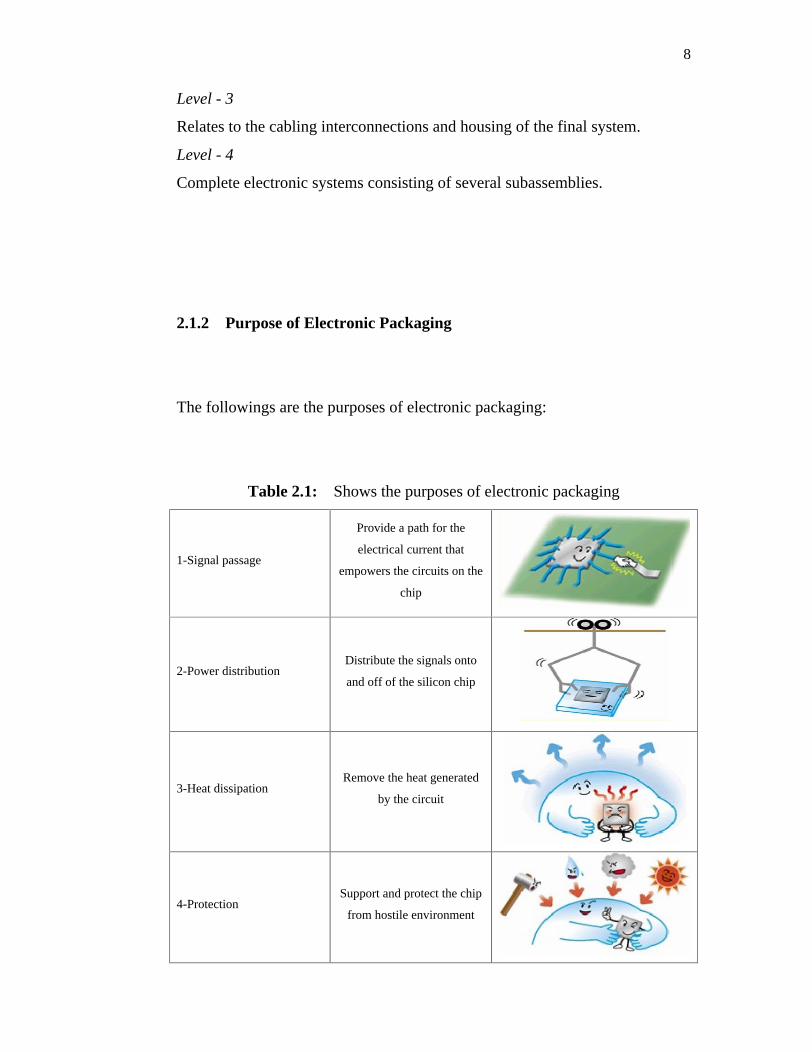
2.1.2 Purpose of Electronic Packaging
The followings are the purposes of electronic packaging:
Table 2.1: Shows the purposes of electronic packaging
1-Signal passage
Provide a path for the
electrical current that
empowers the circuits on the
chip
2-Power distribution Distribute the signals onto
and off of the silicon chip
3-Heat dissipation Remove the heat generated
by the circuit
4-Protection Support and protect the chip
from hostile environment

9
2.1.3 Requirement of the Electronic Packaging
There are a large number of requirements that an electronic package has
to fulfill, such as:
a) Mechanical requirements
These may involve constraints on the structure and thermal characteristics of
the supporting substrate. The substrate is a base material that provides a
supporting surface for deposited or etched wiring patterns - for attachment of
component parts or for fabrication of a semiconductor device.
b) Input/Output (I/O) requirements
These vary significantly depending on the system of interest. For example, the
I/O ports for a hand-held calculator are the keyboard and the display. By
contrast, in a large computer system the I/O ports may include tape drives,
disk drives, printers, etc.
c) Environmental requirements
Tolerance of the packaging to operating conditions such as air humidity and
exposure to chemicals.
d) Reliability requirements
The system's ability to operate for many years with very few problems
e) Interconnection requirements
The number of I/O ports that are needed to provide inter-chip communication,
i.e. between chips and the supporting substrate.

10
2.1.4 Interconnection execution
An interconnection is the conductive path required to achieve
connection from one circuit element to another or to the rest of the circuit
system. Such interconnections may be pins, terminals, formed conductors, or
any other mating system. At the chip level, interconnects are needed to
connect the different electronic circuit elements implemented on or in the chip
such as transistors, capacitors, etc. There are three types of interconnection in
electronic packaging (Figure 2.2):
Figure 2.2 Three types of interconnection in electronic packaging

11
2.1.4.1 Wire Bonding Interconnection
It is the oldest method, but is still the dominant method used today,
particularly for chips with a moderate number of inputs/outputs (I/O). Wire
bonding is an electrical interconnection technique using thin wire and a
combination of heat, pressure and/or ultrasonic energy. It is a type of welding
process whereby two metallic materials, which is the wire and pad surface, are
brought together in an intimate contact. The process begins with the backside
of the chip being firmly attached to the substrate by means of using organic
adhesives, low melting point glasses or a solder. Then the wires are bonded or
welded, one at a time between the chip bonding pads and the appropriate
package or substrate interconnection points. The type of material used for the
wires are usually gold, aluminum and copper. Three major wire bonding
methods can be defined: thermocompression bonding, ultrasonic bonding and
thermosonic bonding. There are two different options of wire bonding, either
ball bonding or wedge bonding. The structure of a wire bond assembly is
shown in Figure 2.3.
Figure 2.3 Wire bonding

12
The advantages and disadvantages of wire bonding interconnection:
Advantages
1- Low cost
2- It is commodity unlike the advanced die attach platforms for flip chip
bonding
3- It is extremely flexible-changes in die size can be accommodated without
noticeable additional costs
Disadvantages
1-Low I/O counts due to technology limitations
2- Large bonding pads in order of 100 x 100 µm
3-Large bonding pitch in order of 200 µm
4-The requirement for relatively large quantities of gold
5-Production rat
6-Relatively poor electrical performance
7-Variations in bond geometry
8-Robustness and reliability problems brought about by environmental
conditions
2.1.4.2 Tape-Automated Bonding
Tape automated bonding was initially and originally conceived as a
rapid and robust alternative to wire bonding, during the times when wire
bonding was done manually and slow. TAB is a process of placing bare chips
and bonding a gold bumped die onto a printed circuit board (PCB) by
attaching them to a flexible tape made of polymer material such as polyimide.

13
The film is then moved to the target location and the leads are cut and soldered
to the board. This is followed by the encapsulation of the bare chip with epoxy
or plastic. The structure of a tape automated bonded die assembly is shown in
Figure 2.4. Encapsulation is done to protect integrated circuitry from
mechanical and chemical attack [2].
Figure 2.4 Tape-automated bonded die
Advantages of Tape Automated Bonding
(a) Allows circuit to be physically flexible
(b) Facilitates multi-chip module manufacturing
(c) Shorter production cycle time
(d) Gives better electrical performance with reduced noise and higher
frequency
(e) Reduced weight
(f) Allows the use of smaller bond pads and finer bonding pitch
(g) Suited for high volume production
Disadvantages of Tape Automated Bonding
(a) High capital expense for its equipment since TAB manufacturing requires
a set of machines different from those used by conventional processes
(b) The film must be specially designer or tailor-made for every chip type

14
(c) Difficulty in assembly rework
(d) Package size increases with large I/O counts
2.1.4.3 Flip Chip Bonding
The term flip in this bond originates from the position of the die where
the active face of the chip facing towards the substrate. In flip chip assembly,
interconnection is achieved using a bump structure on the chip and a bonding
material typically on the substrate forming an electrical connection between
chip and substrate. The chip is mounted upside down onto a carrier, module,
or PWB. Electrical connection is made via solder bumps. The solder bumps
are located over the surface of the chip in a somewhat random pattern or an
array so that periphery limitation, such as that encountered in wire bonding,
does not limit the I/O capability. The I/O density is primarily limited by the
minimum distance between adjacent bonding pads on the chip and the amount
of chip area that can be dedicated to interconnection. Additionally, the
interconnect distance between chip and package is minimized since bumps can
essentially be located anywhere on the chip [3]. Figure 2.5 and Figure 2.6
show the flip chip bonding.
Bumps deposited on solder wettable metal terminals on the active
surface of the semiconductor chip that connect on a matching wettable
substrate pad. During chip assembly, the solder bumps are aligned to the
corresponding substrate metal pads and then reflowed at high temperature to
simultaneously form electrical and mechanical connections. During reflow, the
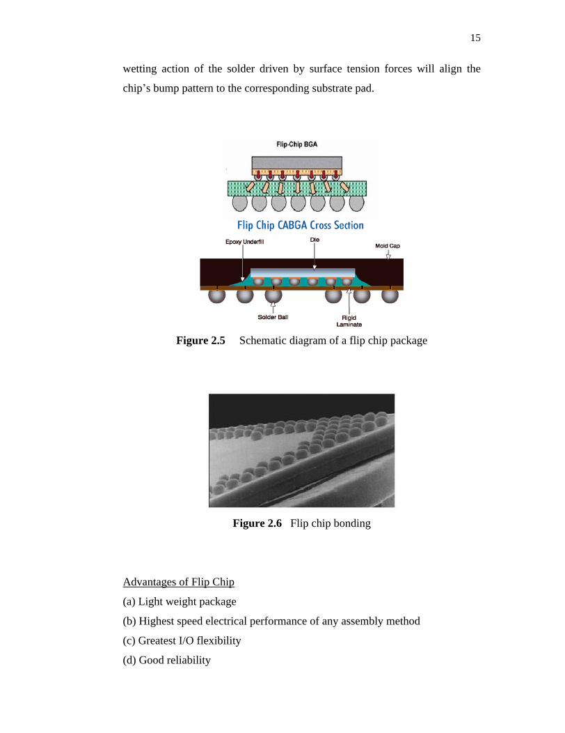
15
wetting action of the solder driven by surface tension forces will align the
chip s bump pattern to the corresponding substrate pad.
Figure 2.5 Schematic diagram of a flip chip package
Figure 2.6 Flip chip bonding
Advantages of Flip Chip
(a) Light weight package
(b) Highest speed electrical performance of any assembly method
(c) Greatest I/O flexibility
(d) Good reliability
16
(e) Lowest cost interconnection for high volume automated production, with
costs below $0.01 per connection.
(f) High density of I/O interconnection per area array packaging
Disadvantages of Flip Chip
(a) High cost for low volume and low I/O packaging
(b) Challenge for PCB technology as pitches become very fine and bump
counts are high
(c) Limited availability of bumped chips.
(d) High assembly accuracy needed.
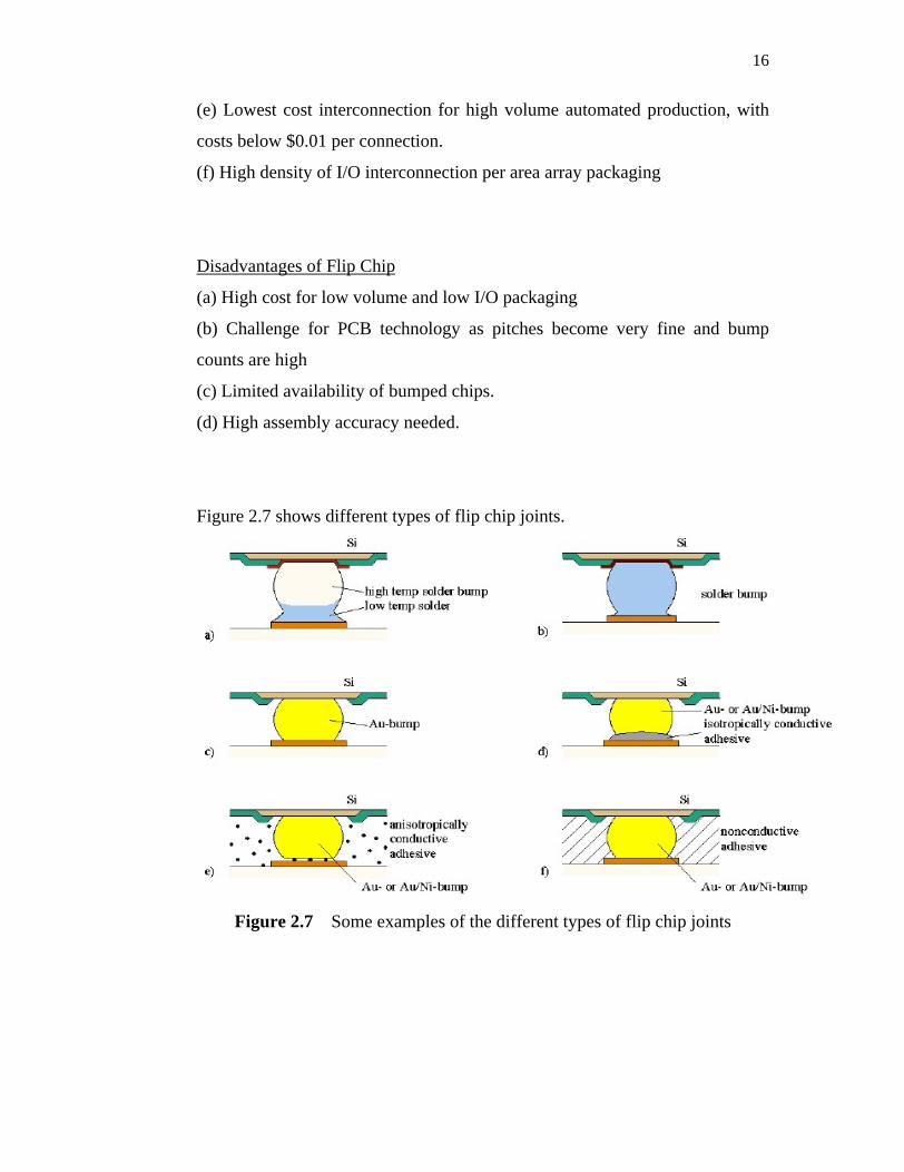
Figure 2.7 shows different types of flip chip joints.
Figure 2.7 Some examples of the different types of flip chip joints

17
2.2 Flip Chip Interconnection
Flip chip joining is not a new technology. IBM has driven the
technology for mainframe computer applications. IBM has processed many
millions of chips on ceramic substrates since the end of 60 s. At the beginning
of 70 s, the automotive industry also began to use flip chips on ceramics.
Today, flip chips are widely used for watches, mobile phones, portable
communicators, disk drives, hearing aids, LCD display, automotive engine
controllers as well as the main frame computers. The number of flip chips
assembled was over 500 million in year 1995 and close to 600 million flip
chips were consumed 1997 [4].
Flip chip describes the method of electrically connecting the die to the
package carrier. The package carrier, either substrate or lead frame, then
provides the connection from the die to the exterior of the package. In
standard packaging, the interconnection between the die and the carrier is
made using wire. The die is attached to the carrier face up, and then a wire is
bonded first to the die, then looped and bonded to the carrier. Wires are
typically 1-5 mm in length, and 25-35 µm in diameter. In contrast, the
connection between the die and carrier in flip chip packaging is made through
a conductive bump that is placed directly on the die surface. The bumped
die is then flipped over: and placed face down, with the bumps connecting
to the carrier directly. A bump is typically 70-100 µm high, and 100-125 µm
in diameter.
The flip chip connection is generally formed either using solder or using
conductive adhesive. By far, the most common packaging interconnects is
solder, in either eutectic (63%Sn, 37%Pb) or high Pb (97%Pb, 3%Sn)

18
compositions. The solder bumped is attached to a substrate by a solder reflow
process, very similar to the process used to attach BGA balls to the package
exterior. After the die is soldered, underfill is added between the die and the
substrate. Underfill is a specially engineered epoxy that fills the area between
the die and the carrier, surrounding the solder bumps. It is deigned to control
the stress in the solder joints caused by the difference I thermal expansion
between the silicon die and the carrier. Once cured, the underfill absorbs the
stress, reducing the strain on the solder bumps, greatly increasing the life of
the finished package. The chip attaches and underfill steps are the basics of
flip chip interconnect. Beyond this, the reminders of package construction
surrounding the die can take many forms and can generally utilize existing
manufacturing processes and package formats. Worldwide flip chip
consumption is over 600,000 units per year, with a projected annual growth
rate of nearly 50% per year. Semiconductors manufacturers currently bump
for flip chip assembly about 3% of wafers produced, and are expected to be
bumping 10% within a few years [5]. Figure 2.8 illustrates the chip is flip
mounted on the package.
Figure 2.8 The chip is flip mounted on the package
19
2.2.1 Production of flip chip
There are three stages in making flip chip assemblies: bumping the die or
wafer, attaching the bumped die to the board or substrate and in most cases,
filling the remaining space under the die with an electrically non-conductive
material. The conductive bump, the attachment materials and the processes
used differentiate the various kinds of flip chip assemblies. The cost,
performance, and space constraints of the application determine which method
best suits it. The following describe the most common bumping and attaching
methods:
Bump Requirements
The bump serves several functions in the flip chip assembly. Electrically,
the bump provides the conductive path from chip to substrate. The bump also
provides a thermally conductive path to carry heat from the chip to the
substrate. In addition, the bump provides part of the mechanical mounting of
the die to the substrate. Finally, the bump provides a spacer, preventing
electrical contact between the chip and substrate conductors, and acting as a
short lead to relieve mechanical strain between board and substrate.
Solder Bump Flip Chip
The solder bumping process first requires that an under bump
metallization (UBM) be placed on the chip bond pads, by sputtering, plating or
other means, to replace the insulating aluminum oxide layer and to define and
limit the solder-wetted area. Solder is deposited over the UBM by evaporation,
electroplating, screen-printing solder paste, or needle depositing. After solder
bumping, the wafer is sawn into bumped die. The bumped die is placed on the
substrate pads, and the assembly is heated to make a solder connection.

20
Plated Bump Flip Chip
Plated bump flip chip uses wet chemical processes to remove the
aluminum oxide and plate conductive metal bumps onto the wafer bond pads.
Plated nickel-gold bumps are formed on the semiconductor wafer by
electroless nickel-plating of the aluminum bond pads of the chips. After
plating the desired thickness of nickel, an immersion gold layer is added for
protection, and the wafer is sawn into bumped die. Attachment generally is by
solder or adhesive, which may be applied to the bumps or the substrate bond
pads by various techniques. Figure 2.9 shows the process of electroplated
bump.
Figure 2.9 Electroplated Bump Process
Stud Bump Flip Chip
The gold stud bump flip chip process bumps die by a modified standard
wire bonding technique. This technique makes a gold ball for wire bonding by
melting the end of a gold wire to form a sphere. The gold ball is attached to
the chip bond pad as the first part of a wire bond. To form gold bumps instead
of wire bonds, wire bonders are modified to break off the wire after attaching
the ball to the chip bond pad. The gold ball, or "stud bump" remaining on the
bond pad provides a permanent connection through the aluminum oxide to the
underlying metal. The gold stud bump process is unique in being readily
applied to individual single die or to wafers. Gold stud bump flip chips may be

21
attached to the substrate bond pads with adhesive or by thermosonic gold-to-
gold connection. Figure 2.10 illustrates the schematic of stud bump.
Figure 2.10 Stud Bump
Adhesive Bump Flip Chip
The adhesive bump flip chip process stencils conductive adhesive to form
bumps on an under-bump metal. The cured adhesive acts as bumps.
Attachment is by an additional layer of conductive adhesive.
Flip Chip Underfill
As described above, one function of the bump is to provide a space
between the chip and the board. In the final stage of assembly, this under-chip
space is usually filled with a non-conductive "Underfill" adhesive joining the
entire surface of the chip to the substrate.
The underfill protects the bumps from moisture or other environmental
hazards and provides additional mechanical strength to the assembly.
However, its most important purpose is to compensate for any thermal
expansion difference between the chip and the substrate. Underfill
mechanically "locks together" chip and substrate so that differences in thermal
expansion do not break or damage the electrical connection of the bumps.
Underfill may be needle-dispensed along the edges of each chip. Cross
22
sections of flip chip joints without and with underfill material shows in Figure
2.11. It is drawn into the under-chip space by capillary action, and heat-cured
to form a permanent bond.
Figure 2.11 Cross sections of flip chip joints without and with underfill
material [6]
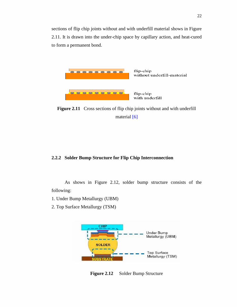
2.2.2 Solder Bump Structure for Flip Chip Interconnection
As shows in Figure 2.12, solder bump structure consists of the
following:
1. Under Bump Metallurgy (UBM)
2. Top Surface Metallurgy (TSM)
Figure 2.12 Solder Bump Structure
23
2.2.2.1 Under Bump Metallization
Under bump metallization (UBM) is an essential part of low-cost solder
flip chip technology. The main functions of UBM are to provide an excellent
solderable surface and to act as a diffusion barrier to protect the underlying
copper from reacting with the solder. In the absence of effective UBM, the
solder reacts with copper and forms intermetallic compounds (IMC) rapidly.
Formation of a thin layer of IMC during soldering is desirable to achieve good
metallurgical bond. However, excess growth of these IMC affects the
mechanical reliability of the joint, which is a generic reliability problem in flip
chip solder joints [4-6]. This IMC growth is influenced by operating
temperature of the device, which is currently in the range of 40 to 150.8 oC [7].
As the trend of miniaturization continues, the increase in operating
temperature will speed up the IMC growth further. Pb-containing solders are
the most suitable materials for flip chip interconnect. However, due to
environmental concern on Pb, electronic industry has been replacing the Pb-
containing solders with Pb-free solders. Pb-free solders are basically tin rich
alloys constituting one or two more elements such as Ag, Cu, In, Sb, and Bi.
These high-Sn content solders react more rapidly with Cu UBM, forming a
thick layer of Cu Sn IMC. IMC growth weakens the solder joints as IMC are
very brittle in nature and can act as an initiation site for the microcracks.

24
2.2.2.2 Top Surface Metallurgy (TSM)
The lower barrier layer of the TSM, which is also known as under bump
metallization on copper is an essential part of low-cost solder flip chip
technology. Its main functions are to provide excellent solderable surface and
to act as a diffusion barrier to protect the underlying copper from reacting with
the solder. Figure 2.13 shows the top surface metallurgy. In the absence of
TSM, the solder reacts with copper and forms intermetallic compounds rapidly
[6]. Gold/ platinum, silver/ palladium, silver/ palladium / gold and silver/
platinum are used as thick-film TSM pads. Various surface finishes of TSM
will be studied thoroughly in this project.
The three major steps involved in manufacturing flip chip bonds are die
bumping and TSM structure manufacture on the substrate, alignment of the die
and substrate and assembly. The TSM structure and solder bump
manufacturing, called the bumping process, can be implemented using a
variety of methods, including metal masking, photolithography, electroplating
and ultrasonic soldering, maskless bumping and copper bumping.
Figure 2.13: Top surface metallurgy

REFERENCES
[1] Lau, J. H. (1994). Chip on Board Technologies for Multichip Modules. Van Nostrand Reinhold.
[2] Gilleo, K. (2002). Introduction to Electronic Packaging. In: Gilleo, K. ed. Area Array
Packaging Handbook-Manufacturing and Assembly. New York: McGraw-Hill. 3-21.
[3] Baldwin, D. F. (2002). Next-Generation Flip Chip Materials and Processing. In: Gilleo, K.. Area Array Packaging Processes. New York: McGraw-Hill. 1-98.
[4] Rymaszewski, E. J. and Tummala, R. R. (1989). Chip-to-Package Interconnections. In: Tummala, R. R. and Rymaszewski, E. J.. Microelectronics Packaging Handbook. New York: Van Nostrand Reinhold. 1-64.
[5] Koopman, N. G., Reiley, T. C. and Totta, P. A. (1989). Chip-to-Package Interconnections. In: Tummala, R. R. and Rymaszewski, E. J.. Microelectronics Packaging Handbook. New York: Van Nostrand Reinhold. 361-454.
[6] Kumar, A., He, M. and Chen, Z. (2004a). Barrier Properties of Thin Au/ Ni-P Under Bump Metallization for Sn-3.5Ag Solder. Surface & Coatings Technology. 1-4.
[7] Beauvilier, L. (2002). The Quest for the Ultimate Surface Finish. Printed Circuit Design. 132
[8] Vianco, P. T. (1998). An Overview of Surface Finishes and Their Role in Printed Circuit Board Solderability and Solder Joint Performance. Circuit World. 25 (1): 6-24.

136
[9] Cullen, D. (1998). Electroless Nickel-Immersion Gold Deposit Characteristics. Circuits Assembly. 62-67.
[10] Milad, G. and O.Brien, G. (2002). .An Overview of Process and Solderability Performance of HASL Alternatives.. The Board Authority.
[11] Strauss, R. (1994). .Surface Mount Technology.. Oxford: Butterworth-Heinemann.
[12] Carano,M. & Hunt,J.(2003). Improved organic solderability preservatives for mixed metal finishes. CircuiTree, vol. 17(5):23-25
[13] Yee, S. and Ladhar, H. (1998). Reliability Comparison of Different Surface Finishes on Copper. Circuit World. 25(1): 25-29.
[14] Barbetta, M. (2003), Surface Finish: An OEM Perspective. CircuiTree. May 2003. pp. 10-13.
[15] Stasform, E. (2000). Unraveling the Final Finishing Mystery. Circuit Assembly. 56-
62.
[16] Gabe, D. R. (1978). Principles of Metal Surface Treatment and Protection. 2nd ed. Oxford, U. K.: Pergamon Press.
[17] Mallory, G. O. and Hajdu, J. B. (1990). The fundamental Aspects of Electroless Nickel Plating. In: Mallory, G. O. and Hajdu J. B.. Electroless Plating: Fundamentals & Applications. Orlando, Florida: American Electroplaters and Surface Finishers Society. 1-56.
[18] Barker, D. (1993). Transactions Inst. Metal Finishing. 71: 121-125.
[19] Aleksinas, M. J. (1990). Troubleshooting Electroless Nickel Plating Solutions. In: Mallory, G. O., and Hadju J. B.. Electroless Plating: Fundamentals and Applications. New York: Noyes publications/William Andrew Publishing. 101-110
[20] Agarwala, V. (2003). Electroless Alloy/ Composite Coatings: Review. Sadhana. 28: 475-493.
[21] Haga, M., Tsuji, K., Nawafune, H., Mizumoto, S. and Uchida, E. (1989). Palladium-base Electroless Plating Solution. (U. S. Patent 4, 804, 410).

137
[22] Baudrand, D. and Bengston, J. (1995). Electroless Plating Processes. Metal
Finishing. Elsevier Science Inc. 55-57.
[23] Duffek, E. F. (1974). Semiconductors and Microelectronics. In: Reid, F. H. and Goldie, W.. Gold Plating Technology. Glasgow: Electrochemical Publications Limited. 495-532.
[24] Parker, E. A., (1974). Immersion Solutions. In: Reid, F. H. and Goldie, W.. Gold Plating Technology. Glasgow: Electrochemical Publications Limited. 73-81.
[25] Garte, S. M. (1974). Porosity. In: Reid, F. H. and Goldie, W.. Gold Plating Technology. Glasgow: Electrochemical Publications Limited. 295-315.
[26] Ronka,K.J., Loo,F.J.J., and Kivilahti,J (1997). The Local Nominal Composition . Useful Concept for Microjoining and Interconnection Applications. Science Materials. 37(10): 1575-1581.
[27] Bentzen,B.S., (2000). Reflow Soldering SMT in FOCUS. p2-3
[28] Mizumoto, S., Nawabune, H., Haga, M. and Tsuji, K. (1986). Extended Abstracts of
Papers Presented at the 73rd
Tech. Conference. Metal Finish. Soc. Japan. 27B-8: 116.
[29] Hwang, J. S. (1992). Solder Paste in Electronics Packaging. New York: Van Nostrand Reinhold
[30] Tai Siew Fong (2003). Materials Interaction During Metallic Interconnection Process. Universiti Teknologi Malaysia: M. Eng. Thesis
[31] Suganuma, K. (2001). Advances in Lead-free Electronics Soldering. Solid State & Material Science. 5: 55-64
[32] Kim, K. S., Huh, S. H., and K. Suganuma. (2003). Effects of Intermetallic Compounds on Properties of Sn-Ag-Cu Lead-Free Soldered Joints. Journal of Alloys and Compounds. 352, Pg. 226

138
[33] Sang Wong Jeong, Jong Hoon Kim, and Hyuck Mo Lee. (2004). Effect of Cooling Rate on Growth of the Intermetallic Compound and Fracture Mode of Near-Eutectic Sn-Ag-Cu/Cu Pad: Before and After Aging. Journal of Electronic Materials. Vol. 23, No.12. Pg 1531
[34] Henderson, D. E., Sung, K. K., Goldsmith, C. and Puttlitz, K. J. (2002). Ag3Sn Plate Formation in the Solidification of Near Ternary Eutectic Sn-Ag- Cu alloys. New York: IBM Corporation
[35] Cullen, D. P., Millad. G. (2004). Implementation of Immersion Silver PCB Surface Finish in Compliance With Underwriters Laboratories.
[36] Azmah Hanim, M.A. 2007. Interfacial Reaction Between Sn-37Pb and Sn- 4Ag-0.5Cu Solder On Different Surface Finish. UTM: PhD thesis
[37] Wang, F.J., Yu, Z.S. & Qi, K. 2007. Intermetallic Compound Formation at Sn3.0Ag 0.5Cu 1.0Zn Lead-Free Solder Alloy/Cu Interface During As- Soldered And As-Aged Conditions. The Journal of Alloys and Compounds; vol. (438), p.110-115
[38] Yu, D.Q & Wang, L. 2007. The Growth and Roughness Evolution of Intermetallic Compounds of Sn Ag Cu/Cu Interface during Soldering Reaction. Journal of Alloys and Compounds
[39] Kang, S.K, Lauro, P.A, Shih, D.Y, Henderson, D.W & Puttlitz, K.J. 2005. Microstructure and Mechanical Properties of Lead-Free Solders and Solder Joints Used In Microelectronic Applications. IBM J. Research and Development; vol. (49) no. 4/5
[40] Don-Son Jiang, Yu-Po Wang and C.S. Hsiao Siliconware Precision Industries Co., Ltd.2006 Effect of Minor Doping Elements on Lead Free Solder Joint Quality No. 123, Da Fong Rd., Tantzu, Taichung, Taiwan, R.O.C