Embed Size (px)
Citation preview
1
Scanning Tunneling Microscopy of Gate Tunable Topological
Insulator Bi2Se3 Thin Films
Tong Zhang1,2, Niv Levy1, Jeonghoon Ha1,2,3, Young Kuk3, and Joseph A. Stroscio1*
1Center for Nanoscale Science and Technology, NIST, Gaithersburg, MD 20899, USA 2Maryland NanoCenter, University of Maryland, College Park, MD 20742, USA
3 Department of Physics and Astronomy, Seoul National University, Seoul, 151-747, Korea
Electrical field control of the carrier density of topological insulators (TI) has greatly
expanded the possible practical use of these materials. However, the combination of low
temperature local probe studies and a gate tunable TI device remains challenging. We have
overcome this limitation by scanning tunneling microscopy and spectroscopy measurements
on in-situ molecular beam epitaxy growth of Bi2Se3 films on SrTiO3 substrates with
pre-patterned electrodes. Using this gating method, we are able to shift the Fermi level of
the top surface states by ≈250 meV on a 3 nm thick Bi2Se3 device. We report field effect
studies of the surface state dispersion, band gap, and electronic structure at the Fermi level.

2
Three-dimensional (3D) topological insulators (TI) are a novel state of matter which
has a bulk band gap but topologically protected metallic surface states [1,2]. Angle
resolved photoemission (ARPES) [3–6] and scanning tunneling microscopy (STM) [7–10]
have confirmed the existence of these surface states in various compounds. These protected
surface states are helical Dirac fermions which are predicted to host many striking quantum
phenomena [1,2]. However, in order to fully utilize the unique properties of these surface
states, the Fermi level (EF) needs to be close to the Dirac Point (ED) and tunable across it.
Unfortunately, three-dimensional TI, like Bi2Se3 and related materials, are usually heavily
doped narrow gap semiconductors, with the Fermi level away from Dirac point. While bulk
and surface chemical doping have been used to tune EF, it is preferable to tune the carrier
density using a gate induced electric field, as recently demonstrated in transport
experiments [11–16]. However, the combination of local probe studies of the density of
states using STM and a gate tunable TI device remains challenging, mostly due to the
environmental sensitivity of TI materials [17]. Unlike graphene, ex-situ fabrication and
processing will significantly degrade the surfaces of TI materials, making them inaccessible
to STM. In addition to simply shifting EF, the electric field is capable of altering the surface
band structure of ultrathin TI films, where the top and bottom surface states are coupled, and
a hybridization gap opens at the Dirac point [18–21]. As a consequence, it might be
possible to observe a topological phase transition in these systems by applying an electric
field perpendicular to the plane of the film, as suggested by recent calculations [21].
In this work, we demonstrate the fabrication of gate-tunable 3D TI devices that are

3
suitable for STM studies. Thin Bi2Se3 films are epitaxially grown on SrTiO3 (STO) (111)
substrates pre-patterned with Pt electrodes, which are mounted on specially designed sample
holders (Fig. 1). The preparation of the STO substrates is crucial for good quality film
growth and a gate insulator that maintains high resistance. The STO (111) substrates were
cleaned by the method described in Ref. [22]. STO pieces, (3×4×0.1) mm3, were
immersed in hot deionized water (70 °C) with ultrasonic agitation for 30 min. The pieces
were then annealed in a tube furnace at 1000 °C for 1 h under a pure O2 atmosphere. After
this two-step treatment, the STO surface is completely cleaned and ambient atomic force
microscopy (AFM) images show flat and regular terraces (Fig. 2(a)). Additionally this
treatment results in highly insulating STO, which is crucial for using it as a gate dielectric.
After cleaning, two rectangular Pt electrodes (50 nm thick) were deposited on the top surface
of the STO substrate to ensure good electrical contacts to the TI film. Another Pt electrode,
serving as a back gate, was deposited on the bottom surface of STO. The pre-patterned STO
piece was mounted into an Al2O3 based sample holder which has multiple tungsten clips for
sample wiring and a tungsten spring clip to hold the sample, which also doubles as a gate
contact (Fig. 1). The whole device is fully compatible with ultra-high vacuum and can be
degassed to 600 °C. Prior to film growth, the STO and sample holder were degassed for 30
min at 500 °C to remove adsorbed gases. The reflection high-energy electron diffraction
(RHEED) pattern gave clean 3×3 surface reconstruction patterns of STO (111) (Fig. 2(b)).
Growth of Bi2Se3 films was carried out by co-evaporating pure elemental (99.9999%) Bi and
Se from Knudsen cells, using a 1:10 flux ratio (Bi:Se) to reduce Se vacancies. The STO
4
substrates were kept at 250 °C during growth. RHEED patterns (Fig.2(c)) measured during
growth show 1×1 streaks, an indication of good crystal quality. The samples were then
transferred in-situ into a STM directly after growth, which avoids any ex-situ post processing.
The experiments were performed in a custom designed STM operating at 5 K, which is
connected to the MBE systems [23]. Due to the large dielectric constant of STO at low
temperatures (≈104), we were able to change the carrier density on the order of 1013 cm-2 at a
gate voltage of 100 V. Note, this corresponds to a similar density change in graphene
obtainable with a gate insulator of 300 nm thick SiO2 at 100 V, but we are able to reach
similar densities with 100 µm thick STO crystal due to the large dielectric constant.
Bi2Se3 has a layered structure consisting of Se-Bi-Se-Bi-Se quintuple layers (QL),
where the bonding between adjacent quintuple layers is weak [24]. In this paper we focus
on three QL thick Bi2Se3 samples, since gating is more effective on thinner films. Figure
2(d) shows the STM topography of a nominal 3QL thick film with flat terraces and 1 nm step
heights, corresponding to one QL. Figure 3(a) shows the two-terminal resistance measured
during sample cool-down, which displays an insulating behavior with resistance increasing
about two orders of magnitude between room temperature and 5 K. Similar insulating
behavior has always been seen in ultrathin Bi2Se3 films, which could be due to strong
interactions [25], or Anderson localization [26,27]. To test the gating ability of the
TI/STO device, we measured the 2-terminal resistance through the 3QL film vs. gate voltage
(Fig. 3(b)). The resistance increases at negative gate voltage as expected for an n-type
doped grown film. However, a maximum is not observed which indicates that we were

5
unable to place the Dirac point at the Fermi level even with -300 V applied to the gate
electrode (Fig. 3(b)).
The gating effect was then locally characterized by scanning tunneling spectroscopy.
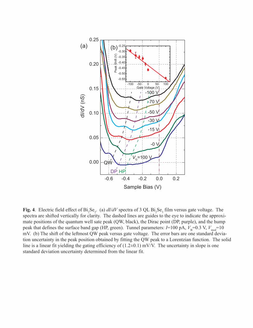
The tunneling conductance dI/dV is measured by standard lock-in techniques and is shown in
Fig 4(a) for different gate voltages VG. At VG = 0 V, there is a “V” shaped structure in the
dI/dV spectra with a minimum at a sample bias VB ≈ -0.4 V, which is typical for Bi2Se3 and
was presumably attributed to the surface Dirac cone. [9,28]. An additional feature seen in
the spectra is a peak at VB ≈ -0.5 V at VG = 0 V, which most possibly comes from a quantum
well (QW) state of the thin film, as seen in similar 3D TIs [29], followed by a strong upturn
due to the onset of the valence band top. At positive bias a kink in the spectrum is observed
at EF (VB= 0V) followed by an upturn.
Application of a gate electric field causes a shift of the spectra as observed in Fig. 4(a).
A downward sweep of gate voltage is accompanied by the Dirac point shifting to higher
energies relative to the Fermi level at 0 V, which is a direct signature of tuning of the carrier
density by the applied electric field. To quantify the gating efficiency we plot the peak
position of the QW peak vs. gate voltage in Fig. 4(b)). A linear fit to the data in Fig. 4(b))
gives a gating efficiency of (1.2±0.1) mV/V [30]. At 100 V applied gate potential, the
resulting Dirac point shift is 120 meV, which gives a density change of surface carriers of ≈
0.4x1013 cm-2 (assuming a linear Dirac spectrum with velocity 5x10⁵ m/s). Assuming a
simple capacitor model we expect a gate capacitance of 2G 0 / 620 μF/mC tε ε= = , where 0ε
is the permittivity of free space, t is the thickness (0.1 mm) and 7000ε ≈ is the dielectric

6
constant of STO [31]. This gate capacitance should induce a charge density of ≈4x10¹³
cm-2 at VG = 100 V. However, we observe an induced density that is ten times less, and one
that is not sufficient to overcome the initial film doping and place the Dirac point at EF at VG
= -100 V. This accounts for the lack of a maximum in the resistance vs. gate voltage plot in
Fig. 3(b). We attribute the reduced gating efficiency of the top surface states, which
decreases with increasing thickness, as due to screening by the degenerately doped bulk
Bi2Se3 film, which screens the electric field at the top surface. As STM is mostly sensitive
to top surface, the shift of the bottom surface’s Dirac point may be larger than that of the top
surface. The high initial doping of the film is probably due to defects produced in growth,
which is common in MBE growth of Bi2Se3 films as well as bulk synthesized crystals. The
mixed compound Bi2Te2Se has been found to be a more insulating material [32], and hence
may respond better to our gating scheme.
In a 3QL Bi2Se3 film, a hybridized gap is expected to open at the Dirac point due to the
coupling of top and bottom surface states [18], which has been observed in ARPES
measurements [6]. Evidence of a gap opening can be seen in the spectra in Fig. 4(a),
where a gap is seen between the QW state peak and the broad hump to the right of the Dirac
minimum, as outlined by the dashed lines. The gap size is about 160 meV, and roughly
matches the ARPES data [6]. However, the gap is not well defined when the spectra shifts
to larger negative energies and higher doping.
In addition to gate dependent features in the spectra, we observe a gate independent kink
in the tunneling spectra at EF (Fig. 4(a)). Similar DOS kinks around EF have been widely
7
observed in Bi2Se3, for both thin film and bulk samples [9,10], and were typically
considered to be the onset of the conduction band. However, the gate independence of the
feature shown here contradicts that explanation and strongly suggests it stems from a
different mechanism, such as the many body effects in 2D Dirac systems [33,34]. One
possible mechanism would involve the surface plasmon mode which has been predicted to
exist in graphene and TI surfaces [33]. Below EF, the electron-plasmon interaction can
lead to reconstruction of the Dirac cone by forming a plasmaron band, which gives a sudden
DOS change at Fermi level [33]. This mechanism which depends on interactions far from
the Dirac point may remain intact despite the opening of a gap around it [19], and may even
be enhanced in ultrathin film geometries [25].
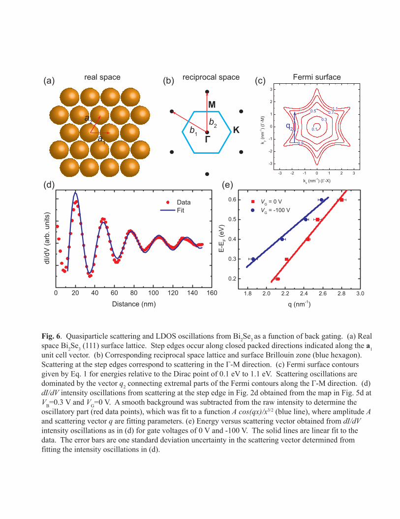
To further explore the gating effects on the surface state band structure, we studied the
quasi-particle interference (QPI) pattern at different gate voltages. Fig. 5, (a)-(e) and (f)-(j)
show the dI/dV mapping of the energy resolved local density of states (LDOS) at a step edge
in Fig. 2(d) at VG = 0 and VG = -100 V, respectively. Within the bias range of 0.2 V to 0.6 V,
standing wave patterns at the step edges are clearly observed, while below 0.2 V we could not
observe a clear interference pattern. At biases close to the Dirac point, scattering is
weakened due to topological protection, despite the opening of a gap at the Dirac point [19].
The data in Fig. 5 covers a bias range that is far from the Dirac point (ED is at VB = -0.4 V for
VG = 0 V), and the constant energy contours of the surface states are hexagonally warped at
these energies [35,36], which enhances the scattering.
The QPI periods in Fig. 5 are seen to depend on gate voltage. We analyze these
8
patterns by considering the scattering geometry and Fermi surface contours in Fig. 6. Step
edges occur along the closed packed directions in the lattice (Fig. 6(a)), and therefore the
scattering in Fig. 5 across the steps in Fig. 2(d) represents scattering in the MΓ − direction
(Fig. 6(b)). The energy contours for Bi2Se3 can be estimated from the energy dispersion
which describes the warping given by [35],
2 3 2( ) ( ) ( cos3 )kE k vk kλ θ± = ± + (1)
where v is the Dirac velocity, λ is the warping parameter, and 1tan ( / )k y xk kθ −= is the
azimuthal angle of the momentum with respect to x axis ( )KΓ − . The energy contours
using Eq. 1 for Bi2Se3 with λ=128 eV Å3 and v=3.55 eV Å [36] are shown in Fig. 6(c).
Above 0.3 eV relative to the Dirac point the contours deviate from circular symmetry. The
data in Fig. 5 cover the energy range of approximately 0.6 eV to 1.0 eV where significant
warping is observed in Fig. 6(c). In these warped contours the dominant scattering vector is
q2 connecting extremal parts of the Fermi surface (Fig. 6(c)) [35,37,38]. To determine the
scattering vectors q2 we fit the dI/dV intensity oscillations to a power-law decay,
3/22cos( ) /A q x x [38], as shown in Fig. 6(d). The resulting E vs. q dispersion is plotted for
two gate voltages in Fig. 6(e). The dispersions are offset from each due to the shift of the
Dirac point with gate potential. We recover the E vs. k dispersion by connecting the
scattering vectors to the momentum k. Recent calculations [38] have shown that q2=1.5 k,
where k is measured from Γ. The resulting dispersion is shown in Fig. 7, where both the VG
= 0 V and VG = -100 V data collapse onto a single curve when the energy is measured from
the Dirac point. A linear fit to this data gives the local curvature of the E-k dispersion of the
9
surface states with a velocity of (1.1±0.1) x 106 m/s. This velocity is almost twice the
velocity determined at lower energies on thick films with a linear dispersion [38]. At this
high energy above the Dirac point the dispersion is expected to be no longer linear due to
warping and also due to the finite band gap [6], which may account for the increase in the
local velocity determined from the QPI measurements.
In summary, we have successfully fabricated in-situ gate tunable epitaxial Bi2Se3 films.
We have studied the effects of the gate’s electric field as expressed in the shifts of spectral
features in the tunneling spectra and in QPI scattering periods. While the current gating
effectiveness is limited in Bi2Se3 due to bulk doping, the combination of in-situ MBE, STM,
and transport studies in TI devices opens new avenues for future work in more insulating
samples.

10
Figure Captions
Fig. 1. 3D computer-automated drawings of the high temperature sample holder with in situ back gating capability. (a) Top view. (b) Cross-sectional view. Part list: (1) alumina sample holder, (2) W source/drain electrode (tunnel bias), (3) W source/drain electrode, (4) SrTiO3 substrate, (5) Pt electrodes on SrTiO3, (6) Pt back gate electrode on SrTiO3, (7) W spring clip to hold SrTiO3, (8)W back gate electrode. Fig. 2. Characterization of the SrTiO3 substrate for TI growth. (a) AFM image, 1 μm x 1 μm, of SrTiO3 after thermal processing as detailed in the text showing large atomically flat terraces separated by single atomic-height steps. (b) RHEED pattern of SrTiO3 prior to TI growth. (c) RHEED pattern of 3 QL Bi2Se3 film grown on SrTiO3. (d) STM topographic image, 81 nm x 81 nm, of 3 QL Bi2Se3 film grown by MBE on the gated sample holder in Fig. 1. The arrow indicates the position of dI/dV mapping of quasiparticle scattering in Fig. 5. Tunneling parameters: VB=1.5 V, I=30 pA. Fig. 3. Transport properties of 3 QL Bi2Se3 film. (a) Bi2Se3 film (3 QL) 2-terminal film resistance versus temperature. (b) Bi2Se3 film (3 QL) 2-terminal film resistance versus gate voltage. Fig. 4. Electric field effect of Bi2Se3. (a) dI/dV spectra of 3 QL Bi2Se3 film versus gate voltage. The spectra are shifted vertically for clarity. The dashed lines are guides to the eye to indicate the approximate positions of the quantum well state peak (QW, black), the Dirac point (DP, purple), and the hump peak that defines the surface band gap (HP, green). Tunnel parameters: I=100 pA, VB=0.3 V, Vmod=10 mV. (b) The shift of the leftmost QW peak versus gate voltage. The error bars are one standard deviation uncertainty in the peak position obtained by fitting the QW peak to a Lorentzian function. The solid line is a linear fit yielding the gating efficiency of (1.2±0.1) mV/V. The uncertainty in slope is one standard deviation uncertainty determined from the linear fit. Fig. 5. Bi2Se3 quasiparticle interference (QPI) patterns from the step edge indicated in Fig. 2d. dI/dV maps of QPI patterns at VG = 0 V (a-d) and VG = -100 V (f-j) at the indicated sample biases. dI/dV intensity is given by the color scale from low (dark) to high (bright) in arbitrary units. The oscillations in the dI/dV maps are used to determine the energy momentum dispersion in Figs. 6 and 7. Tunneling parameters: I=50 pA, VB indicated in each panel, Vmod=15 mV.
Fig. 6. Quasiparticle scattering and LDOS oscillations from Bi2Se3 as a function of back gating. (a) Real space Bi2Se3 (111) surface lattice. Step edges occur along closed packed directions indicated along the a1 unit cell vector. (b) Corresponding reciprocal space lattice and surface Brillouin zone (blue hexagon). Scattering at the step edges correspond to scattering in the Γ-M direction. (c) Fermi surface contours given by Eq. 1 for energies

11
relative to the Dirac point of 0.1 eV to 1.1 eV. Scattering oscillations are dominated by the vector q2 connecting extremal parts of the Fermi contours along the Γ-M direction. (d) dI/dV intensity oscillations from scattering at the step edge in Fig. 2d obtained from the map in Fig. 5(d) at VB=0.3 V and VG=0 V. A smooth background was subtracted from the raw intensity to determine the oscillatory part (red data points), which was fit to a function A cos(qx)/x3/2 (blue line), where amplitude A and scattering vector q are fitting parameters. (e) Energy versus scattering vector obtained from dI/dV intensity oscillations as in (d) for gate voltages of 0 V and -100 V. The solid lines are linear fits to the data. The error bars are one standard deviation uncertainty in the scattering vector determined from fitting the intensity oscillations in (d). Fig. 7. Bi2Se3 energy-momentum dispersion along the Γ-M direction determined from quasiparticle scattering oscillations from step edges. The E vs. q data in Fig. 6(e) at different gate voltages are repotted with energies relative to the Dirac point at VB=-0.4 eV for VG=0 V and VB=-0.27 V for VG=-100 V. The momentum k is determined from the scattering vector as q=1.5k following Ref. 35. The data from the different gate voltages collapse onto the same dispersion. The solid line is a linear fit yielding a velocity = (1.11±0.09) x 106 m/s. The error in the velocity is one standard deviation uncertainty from the linear fit.

12
References
* To whom correspondence should be addressed:[email protected]
[1] M. Z. Hasan and C. L. Kane, Rev. Mod. Phys. 82, 3045 (2010). [2] X.-L. Qi and S.-C. Zhang, Rev. Mod. Phys. 83, 1057 (2011). [3] D. Hsieh, D. Qian, L. Wray, Y. Xia, Y. S. Hor, R. J. Cava, and M. Z. Hasan, Nature 452,
970 (2008). [4] D. Hsieh, Y. Xia, D. Qian, L. Wray, J. H. Dil, F. Meier, J. Osterwalder, L. Patthey, J. G.
Checkelsky, N. P. Ong, A. V. Fedorov, H. Lin, A. Bansil, D. Grauer, Y. S. Hor, R. J. Cava, and M. Z. Hasan, Nature 460, 1101 (2009).
[5] Y. L. Chen, J. G. Analytis, J.-H. Chu, Z. K. Liu, S.-K. Mo, X. L. Qi, H. J. Zhang, D. H. Lu, X. Dai, Z. Fang, S. C. Zhang, I. R. Fisher, Z. Hussain, and Z.-X. Shen, Science 325, 178 (2009).
[6] Y. Zhang, K. He, C.-Z. Chang, C.-L. Song, L.-L. Wang, X. Chen, J.-F. Jia, Z. Fang, X. Dai, W.-Y. Shan, S.-Q. Shen, Q. Niu, X.-L. Qi, S.-C. Zhang, X.-C. Ma, and Q.-K. Xue, Nature Physics 6, 584 (2010).
[7] T. Zhang, P. Cheng, X. Chen, J.-F. Jia, X. Ma, K. He, L. Wang, H. Zhang, X. Dai, Z. Fang, X. Xie, and Q.-K. Xue, Phys. Rev. Lett. 103, 266803 (2009).
[8] Z. Alpichshev, J. G. Analytis, J.-H. Chu, I. R. Fisher, Y. L. Chen, Z. X. Shen, A. Fang, and A. Kapitulnik, Phys. Rev. Lett. 104, 016401 (2010).
[9] P. Cheng, C. Song, T. Zhang, Y. Zhang, Y. Wang, J.-F. Jia, J. Wang, Y. Wang, B.-F. Zhu, X. Chen, X. Ma, K. He, L. Wang, X. Dai, Z. Fang, X. Xie, X.-L. Qi, C.-X. Liu, S.-C. Zhang, and Q.-K. Xue, Phys. Rev. Lett. 105, 076801 (2010).
[10] T. Hanaguri, K. Igarashi, M. Kawamura, H. Takagi, and T. Sasagawa, Phys. Rev. B 82, 081305 (2010).
[11] J. Chen, H. J. Qin, F. Yang, J. Liu, T. Guan, F. M. Qu, G. H. Zhang, J. R. Shi, X. C. Xie, C. L. Yang, K. H. Wu, Y. Q. Li, and L. Lu, Phys. Rev. Lett. 105, 176602 (2010).
[12] J. G. Checkelsky, Y. S. Hor, R. J. Cava, and N. P. Ong, Phys. Rev. Lett. 106, 196801 (2011).
[13] H. Steinberg, D. R. Gardner, Y. S. Lee, and P. Jarillo-Herrero, Nano Lett. 10, 5032 (2010).
[14] D. Kong, Y. Chen, J. J. Cha, Q. Zhang, J. G. Analytis, K. Lai, Z. Liu, S. S. Hong, K. J. Koski, S.-K. Mo, Z. Hussain, I. R. Fisher, Z.-X. Shen, and Y. Cui, Nature Nanotechnology 6, 705 (2011).
[15] S. Cho, N. P. Butch, J. Paglione, and M. S. Fuhrer, Nano Lett. 11, 1925 (2011). [16] D. Kim, S. Cho, N. P. Butch, P. Syers, K. Kirshenbaum, S. Adam, J. Paglione, and M.
S. Fuhrer, Nature Physics 8, 459 (2012). [17] D. Kong, J. J. Cha, K. Lai, H. Peng, J. G. Analytis, S. Meister, Y. Chen, H.-J. Zhang, I.
R. Fisher, Z.-X. Shen, and Y. Cui, ACS Nano 5, 4698 (2011). [18] C.-X. Liu, H. Zhang, B. Yan, X.-L. Qi, T. Frauenheim, X. Dai, Z. Fang, and S.-C.
Zhang, Phys. Rev. B 81, 041307 (2010).
13
[19] H.-Z. Lu, W.-Y. Shan, W. Yao, Q. Niu, and S.-Q. Shen, Phys. Rev. B 81, 115407 (2010).
[20] W.-Y. Shan, H.-Z. Lu, and S.-Q. Shen, New Journal of Physics 12, 043048 (2010). [21] H. Li, L. Sheng, and D. Y. Xing, Phys. Rev. B 85, 045118 (2012). [22] J. Chang, Y.-S. Park, and S.-K. Kim, Applied Physics Letters 92, 152910 (2008). [23] Y. J. Song, A. F. Otte, V. Shvarts, Z. Zhao, Y. Kuk, S. R. Blankenship, A. Band, F. M.
Hess, and J. A. Stroscio, Review of Scientific Instruments 81, 121101 (2010). [24] H. Zhang, C.-X. Liu, X.-L. Qi, X. Dai, Z. Fang, and S.-C. Zhang, Nature Physics 5,
438 (2009). [25] M. Liu, C.-Z. Chang, Z. Zhang, Y. Zhang, W. Ruan, K. He, L. Wang, X. Chen, J.-F. Jia,
S.-C. Zhang, Q.-K. Xue, X. Ma, and Y. Wang, Phys. Rev. B 83, 165440 (2011). [26] Y. S. Kim, M. Brahlek, N. Bansal, E. Edrey, G. A. Kapilevich, K. Iida, M. Tanimura, Y.
Horibe, S.-W. Cheong, and S. Oh, Phys. Rev. B 84, 073109 (2011). [27] A. A. Taskin, S. Sasaki, K. Segawa, and Y. Ando, Phys. Rev. Lett. 109, 066803 (2012). [28] T. Hanaguri, K. Igarashi, M. Kawamura, H. Takagi, and T. Sasagawa, Phys. Rev. B 82,
081305 (2010). [29] Y. Jiang, Y. Y. Sun, M. Chen, Y. Wang, Z. Li, C. Song, K. He, L. Wang, X. Chen, Q.-K.
Xue, X. Ma, and S. B. Zhang, Phys. Rev. Lett. 108, 066809 (2012). [30] The error in the gating efficiency is one standard deviation uncertainty determined from
the linear fit. [31] A. Tkach, O. Okhay, P. M. Vilarinho, and A. L. Kholkin, Journal of Physics:
Condensed Matter 20, 415224 (2008). [32] S. Jia, H. Ji, E. Climent-Pascual, M. K. Fuccillo, M. E. Charles, J. Xiong, N. P. Ong,
and R. J. Cava, Phys. Rev. B 84, 235206 (2011). [33] A. Karch, Phys. Rev. B 83, 245432 (2011). [34] A. Principi, M. Polini, R. Asgari, and A. H. MacDonald, Solid State Communications
152, 1456 (2012). [35] L. Fu, Phys. Rev. Lett. 103, 266801 (2009). [36] K. Kuroda, M. Arita, K. Miyamoto, M. Ye, J. Jiang, A. Kimura, E. E. Krasovskii, E. V.
Chulkov, H. Iwasawa, T. Okuda, K. Shimada, Y. Ueda, H. Namatame, and M. Taniguchi, Phys. Rev. Lett. 105, 076802 (2010).
[37] W.-C. Lee, C. Wu, D. P. Arovas, and S.-C. Zhang, Phys. Rev. B 80, 245439 (2009). [38] J. Wang, W. Li, P. Cheng, C. Song, T. Zhang, P. Deng, X. Chen, X. Ma, K. He, J.-F. Jia,
Q.-K. Xue, and B.-F. Zhu, Phys. Rev. B 84, 235447 (2011).

(1)(2)
(3)(4)
(5)
(a)
(1)
(3)
(4)
(5)
(6)(7) (8)
(b)
Fig. 1. 3D computer-automated drawings of the high temperature sample holder with in situ back gating capability. (a) Top view. (b) Cross-sectional view. Part list: (1) alumina sample holder, (2) W source/drain electrode (tunnel bias), (3) W source/drain electrode, (4) SrTiO3 substrate, (5) Pt electrodes on SrTiO3, (6) Pt back gate electrode on SrTiO3, (7) W spring clip to hold SrTiO3, (8)W back gate elec-trode.

(c)
(b)(a)
250 nm
(d)
20 nm
Fig. 2. Characterization of the SrTiO3 substrate for TI growth. (a) AFM image, 1 μm x 1 μm, of SrTiO3 after thermal processing as detailed in the text showing large atomically flat terraces sepa-rated by single atomic-height steps. (b) RHEED pattern of SrTiO3 prior to TI growth. (c) RHEED pattern of 3 QL Bi2Se3 film grown on SrTiO3. (d) STM topographic image, 81 nm x 81 nm, of 3 QL Bi2Se3 film grown by MBE on the gated sample holder in Fig. 1. The arrow indicates the position of dI/dV mapping of quasiparticle scattering in Fig. 5. Tunneling parameters: VB=1.5 V, I=30 pA.

(a)
(b)
Fig. 3. Transport properties of 3 QL Bi2Se3 film. (a) Bi2Se3 film (3 QL) 2-terminal film resis-tance versus temperature. (b) Bi2Se3 film (3 QL) 2-terminal film resistance versus gate voltage.
-100 V
-70 V
-50 V
-30 V
-15 V
-0 V
VG=100 V
(a)
QW
DP HP
(b)
Fig. 4. Electric field effect of Bi2Se3. (a) dI/dV spectra of 3 QL Bi2Se3 film versus gate voltage. The spectra are shifted vertically for clarity. The dashed lines are guides to the eye to indicate the approxi-mate positions of the quantum well sate peak (QW, black), the Dirac point (DP, purple), and the hump peak that defines the surface band gap (HP, green). Tunnel parameters: I=100 pA, VB=0.3 V, Vmod=10 mV. (b) The shift of the leftmost QW peak versus gate voltage. The error bars are one standard devia-tion uncertainty in the peak position obtained by fitting the QW peak to a Lorentzian function. The solid line is a linear fit yielding the gating efficiency of (1.2±0.1) mV/V. The uncertainty in slope is one standard deviation uncertainty determined from the linear fit.

(a) (b) (c) (d) (e)VG = 0 V
VB = 0.6 V VB = 0.5 V VB = 0.4 V VB = 0.3 V VB = 0.2 V
(f) (g) (h) (i) (j)VG = -100 V
VB = 0.2 VVB = 0.3 VVB = 0.4 VVB = 0.5 VVB = 0.6 V
5 nm
Fig. 5. Bi2Se3 quasiparticle interference (QPI) patterns from the step edge indicated in Fig. 2d. dI/dV maps of QPI patterns at VG = 0 V (a-d) and VG = -100 V (f-j) at the indicated sample biases. dI/dV inten-sity is given by the color scale from low (dark) to high (bright) in arbitrary units. The oscillations in the dI/dV maps are used to determine the energy momentum dispersion in Figs. 6 and 7. Tunneling param-eters: I=50 pA, VB indicated in each panel, Vmod=15 mV.
a1
a2
real space(a)
(d) (e)
(b) (c)
K
M
Γ
b2b1
reciprocal space Fermi surface
q2
Fig. 6. Quasiparticle scattering and LDOS oscillations from Bi2Se3 as a function of back gating. (a) Real space Bi2Se3 (111) surface lattice. Step edges occur along closed packed directions indicated along the a1 unit cell vector. (b) Corresponding reciprocal space lattice and surface Brillouin zone (blue hexagon). Scattering at the step edges correspond to scattering in the Γ-M direction. (c) Fermi surface contours given by Eq. 1 for energies relative to the Dirac point of 0.1 eV to 1.1 eV. Scattering oscillations are dominated by the vector q2 connecting extremal parts of the Fermi contours along the Γ-M direction. (d) dI/dV intensity oscillations from scattering at the step edge in Fig. 2d obtained from the map in Fig. 5d at VB=0.3 V and VG=0 V. A smooth background was subtracted from the raw intensity to determine the oscillatory part (red data points), which was fit to a function A cos(qx)/x3/2 (blue line), where amplitude A and scattering vector q are fitting parameters. (e) Energy versus scattering vector obtained from dI/dV intensity oscillations as in (d) for gate voltages of 0 V and -100 V. The solid lines are linear fit to the data. The error bars are one standard deviation uncertainty in the scattering vector determined from fitting the intensity oscillations in (d).
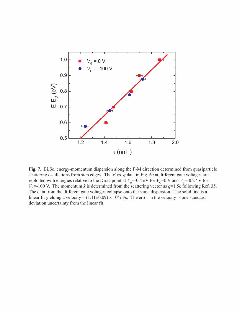
Fig. 7. Bi2Se3 energy-momentum dispersion along the Γ-M direction determined from quasiparticle scattering oscillations from step edges. The E vs. q data in Fig. 6e at different gate voltages are replotted with energies relative to the Dirac point at VB=-0.4 eV for VG=0 V and VB=-0.27 V for VG=-100 V. The momentum k is determined from the scattering vector as q=1.5k following Ref. 35. The data from the different gate voltages collapse onto the same dispersion. The solid line is a linear fit yielding a velocity = (1.11±0.09) x 106 m/s. The error in the velocity is one standard deviation uncertainty from the linear fit.


![Voltage-Controlled Superconducting Quantum Bus · at the end of the tunable bus is made from several gate tunable JJs in parallel [Fig. 2(b)]. The device was fabricated following](https://img.pdfslide.us/doc/110x75/5eabd3da23d2d632a1488868/voltage-controlled-superconducting-quantum-bus-at-the-end-of-the-tunable-bus-is.jpg)