Embed Size (px)
DESCRIPTION
Study of a charge distribution on a readout board with a triple GEM chamber. Shoji Uno (KEK) KEK Detector Technology Project October 31 st , 2006. MPGD group T. Uchida, M. Sekimoto, T. Murakami, M. Tanaka, S. Tanaka, N. Ujiie, and K. Nakayoshi (KEK) - PowerPoint PPT Presentation
Citation preview
Study of a charge distribution on a readout board with a triple GEM chamber
MPGD group T. Uchida, M. Sekimoto, T. Murakami, M. Tanaka, S. Tanaka,
N. Ujiie, and K. Nakayoshi (KEK)K. Kadomatsu and A. Sugiyama (Saga University )
E. Nakano and S. Nakagawa (Osaka City University)
Shoji Uno (KEK)KEK Detector Technology Project
October 31st , 2006
Contents
• GEM foils made by Japanese company
• Effective Gas gain as a function of various parameters
• VGEM, ED, ET,EI, gI
• Gas mixture: Ar-CH4(90/10) (P10)
Ar-CO2(70/30)
• Charge distribution on a readout board
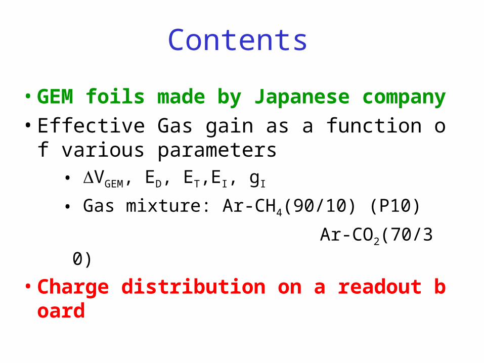
GEM foils made by Japanese company• New method (plasma etching) was tried in a
few years ago. – Not chemical etching (CERN) – M. Inuzuka, et al.,
NIM A 525(2004) 529-534 • Plasma + Laser
– To reduce sparks • It is convenient for us to make new types of
GEM foils.– Fine pitch/small hole : 50m/30m– Thicker/thinner : 100(150)m/ 25m – Other activities in Japan
• Univ. of Tokyo• RIKEN • etc
• Today, I will report on results with standard GEM foils.– 50m thick – 140m pitch 70m diameter
10cm
10cm
Scienergy Co., Ltd. (Japanese company)http://www.scienergy.jp/
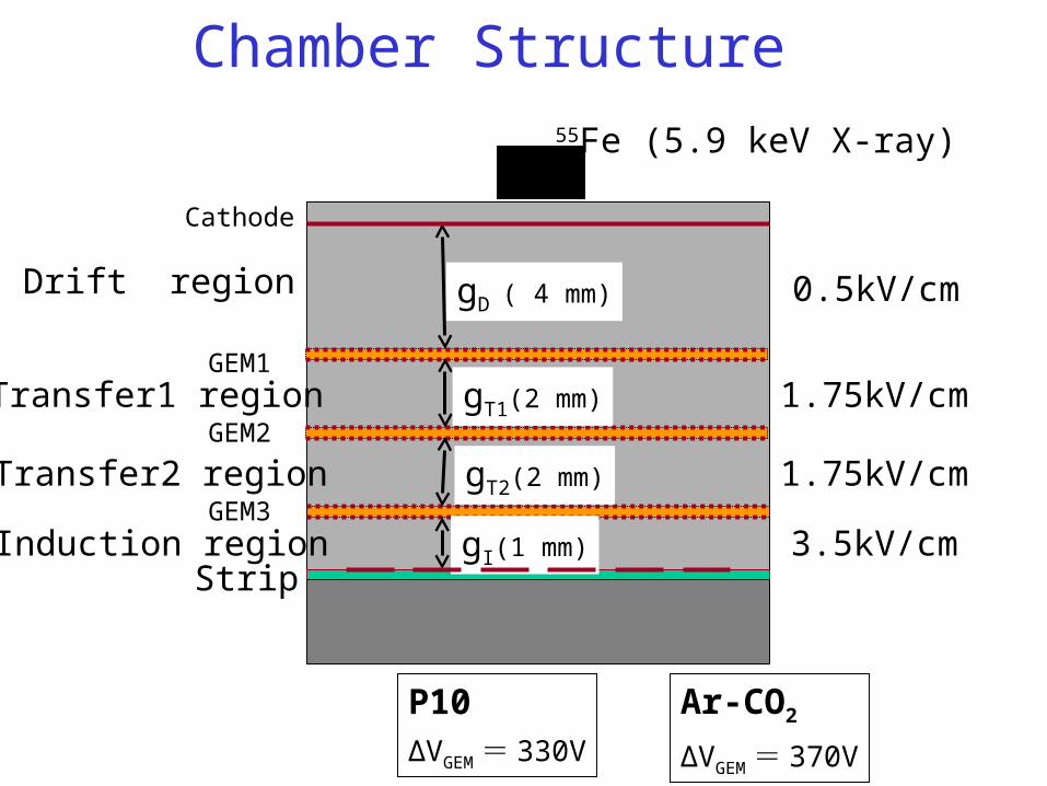
Chamber Structure
gI(1 mm)
gD ( 4 mm)
GEM1
GEM2
GEM3gT2(2 mm)
gT1(2 mm)
55Fe (5.9 keV X-ray)
Cathode
Strip
0.5kV/cm
1.75kV/cm
1.75kV/cm
3.5kV/cm
Drift region
Transfer1 region
Transfer2 region
Induction region
Ar-CO2
ΔVGEM = 370V
P10ΔVGEM = 330V
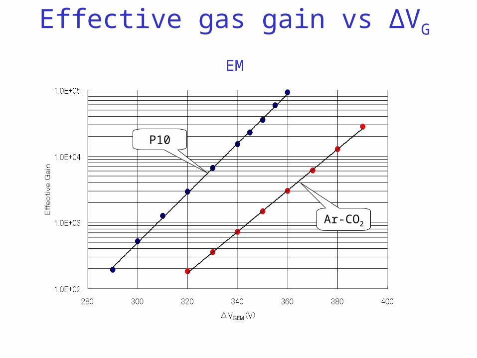
Effective gas gain vs ΔVGEM
Ar-CO2
P10
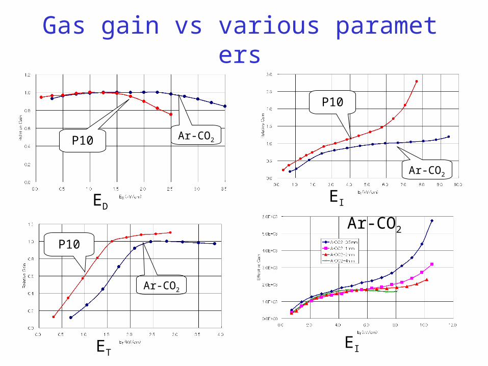
Gas gain vs various parameters
P10
Ar-CO2
Ar-CO2
Ar-CO2
P10
P10
Ar-CO2
EDEI
ETEI
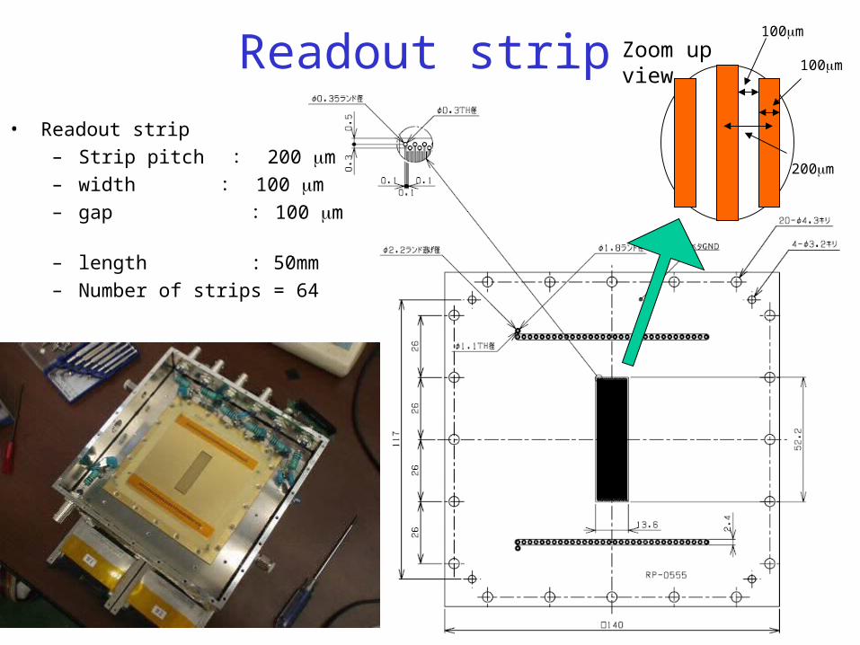
Readout strip
• Readout strip
– Strip pitch : 200 m
– width : 100 m – gap : 100 m – length : 50mm
– Number of strips = 64
Zoom up view100m
100m
200m
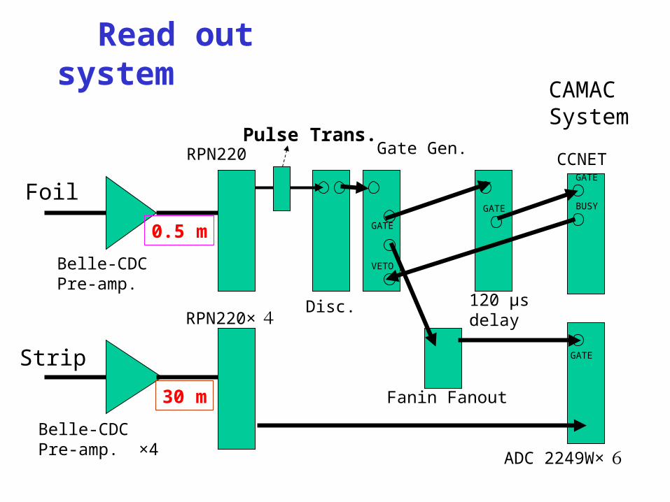
Read out system
RPN220× 4
ADC 2249W× 6
CCNET
GATE
GATE
BUSY
Fanin Fanout
Gate Gen.
GATE
GATE
120 μsdelay
VETO
Disc.
RPN220
Belle-CDCPre-amp. ×4
Belle-CDCPre-amp.
30 m
0.5 m
Strip
Foil
Pulse Trans.
CAMACSystem
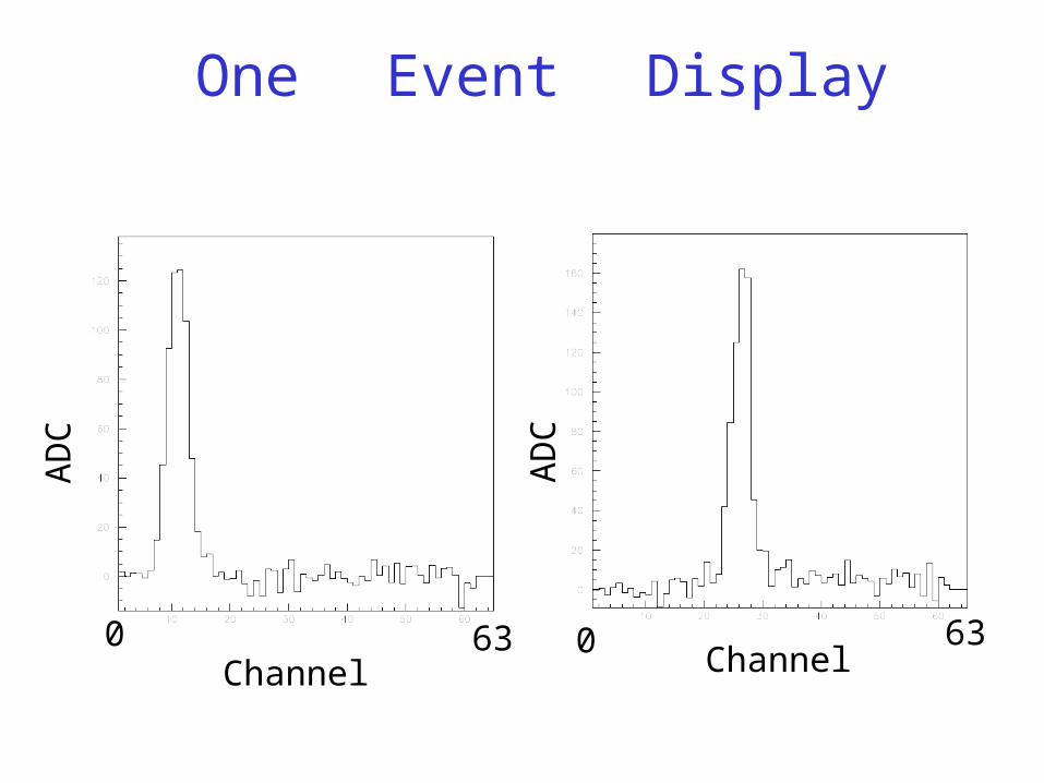
One Event Display
Channel
AD
C
0 63
AD
C
0 63Channel
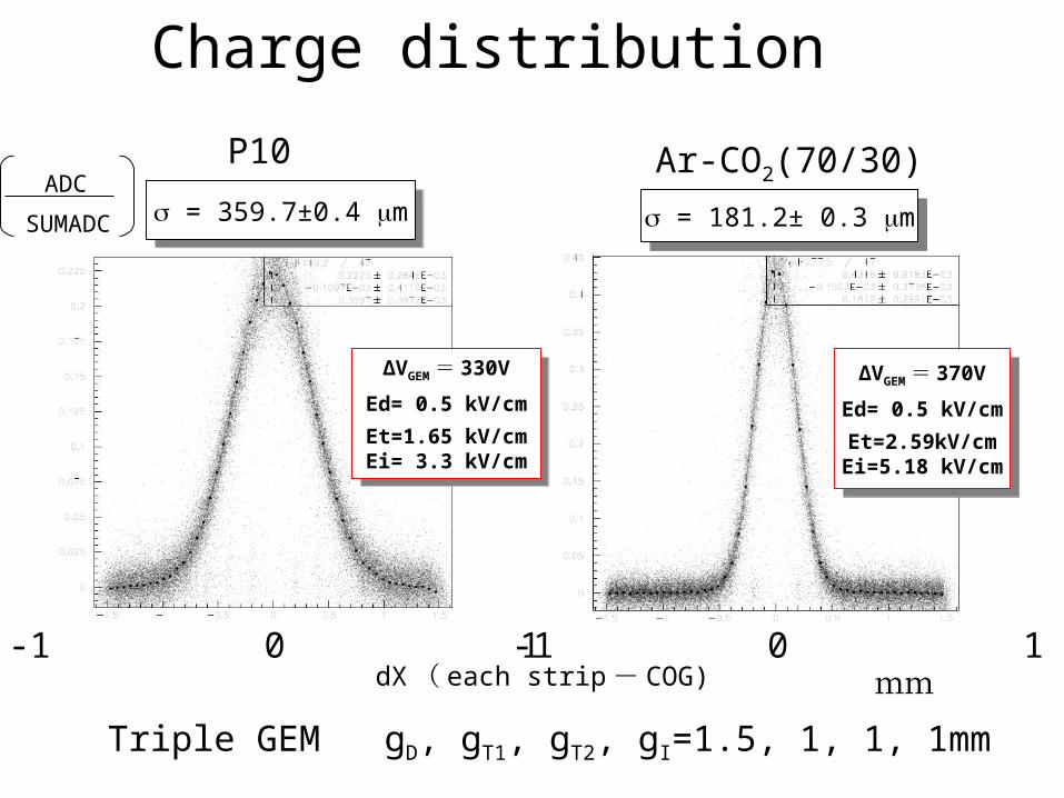
ΔVGEM= 370V
Ed= 0.5 kV/cm
Et=2.59kV/cmEi=5.18 kV/cm
ΔVGEM= 370V
Ed= 0.5 kV/cm
Et=2.59kV/cmEi=5.18 kV/cm
= 181.2± 0.3 m = 181.2± 0.3 m
Ar-CO2(70/30)
Charge distribution
-1 0 1
Triple GEM gD, gT1, gT2, gI=1.5, 1, 1, 1mm
dX ( each strip - COG) mm
= 359.7±0.4 m = 359.7±0.4 m
P10
ΔVGEM= 330V
Ed= 0.5 kV/cm
Et=1.65 kV/cmEi= 3.3 kV/cm
ΔVGEM= 330V
Ed= 0.5 kV/cm
Et=1.65 kV/cmEi= 3.3 kV/cm
ADC
SUMADC
-1 0 1
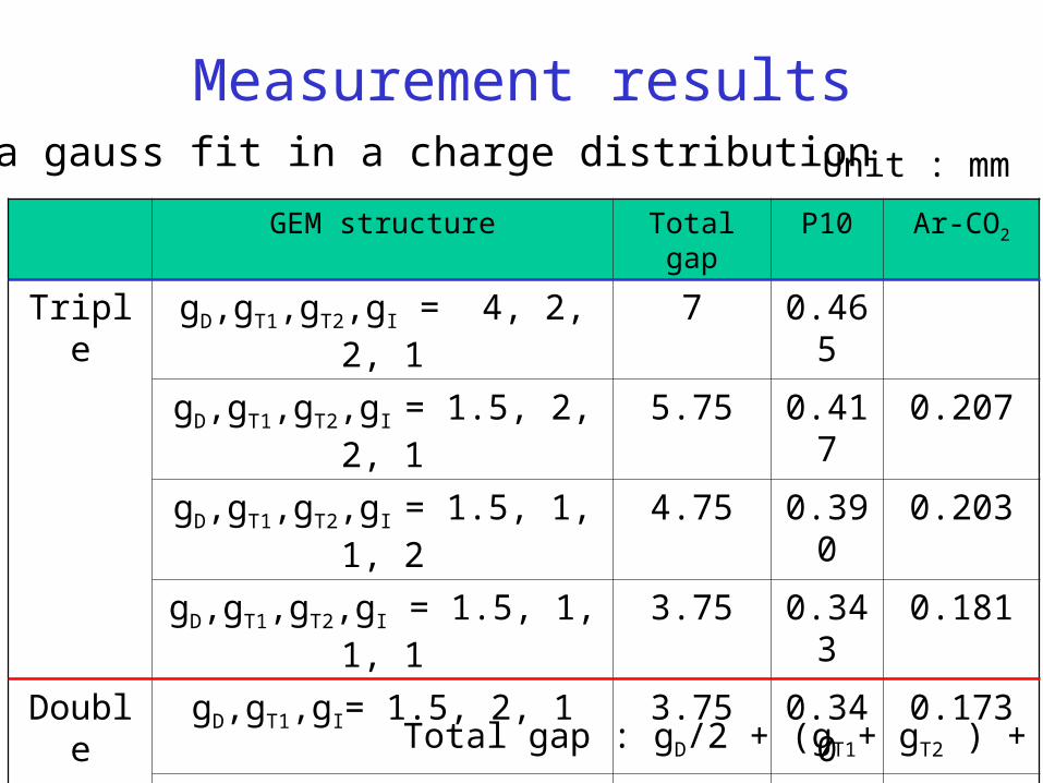
Measurement results for a gauss fit in a charge distribution Unit : mm
GEM structure Total gap P10 Ar-CO2
Triple gD,gT1,gT2,gI = 4, 2, 2, 1 7 0.465
gD,gT1,gT2,gI = 1.5, 2, 2, 1 5.75 0.417 0.207
gD,gT1,gT2,gI = 1.5, 1, 1, 2 4.75 0.390 0.203
gD,gT1,gT2,gI = 1.5, 1, 1, 1 3.75 0.343 0.181
Double gD,gT1,gI= 1.5, 2, 1 3.75 0.340 0.173
gD,gT1,gI = 1.5, 1, 1 2.75 0.157
Total gap : gD/2 + (gT1+ gT2 ) + gI
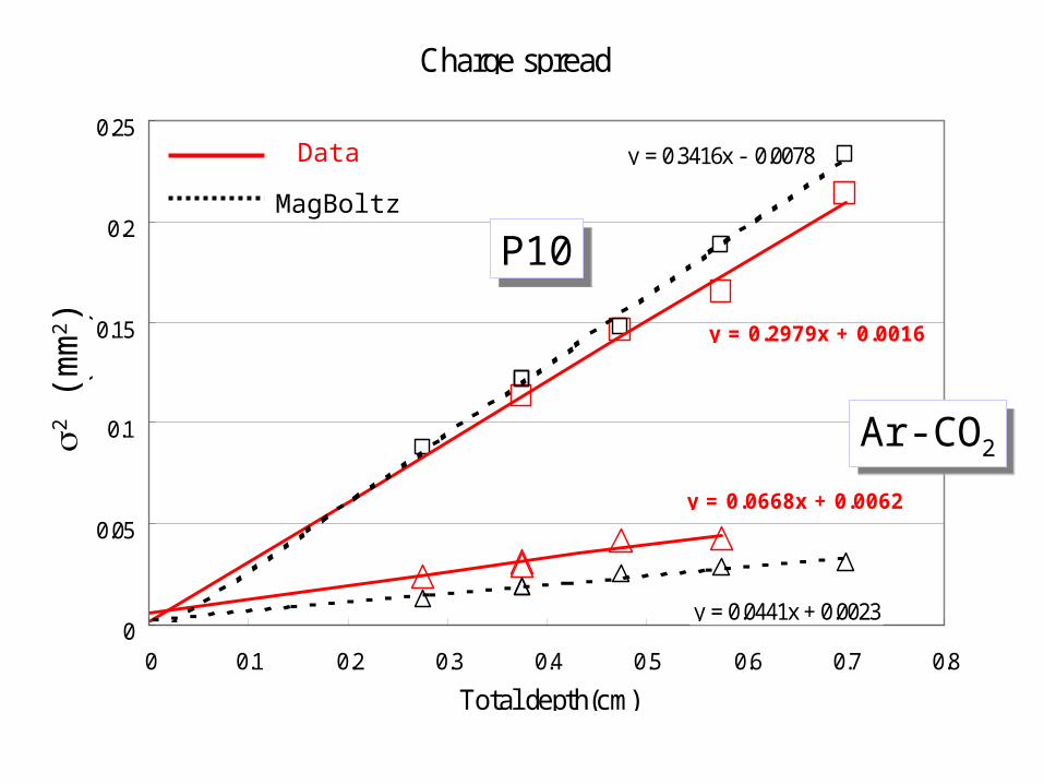
Charge spread
y = 0.2979x + 0.0016
y = 0.0668x + 0.0062
y = 0.3416x - 0.0078
y = 0.0441x + 0.00230
0.05
0.1
0.15
0.2
0.25
0 0.1 0.2 0.3 0.4 0.5 0.6 0.7 0.8
Total depth(cm)
σ2 (
mm
2)
P10P10
Ar-CO2Ar-CO2
Data
MagBoltz
2 (m
m2 )
0.1
0.15
0.2
0.25
0.3
0.35
0.4
0 1 2 3 4
/ cm)電場(kv
σ2 (m
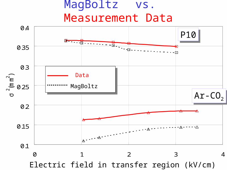
m2 )MagBoltz vs. Measurement
Data
P10P10
Ar-CO2Ar-CO2
Data
MagBoltz
Electric field in transfer region (kV/cm)
Summary• Japanese company can produce GEM foils with
new methods ( Plasma or (and) Laser ).
• GEM chamber has been constructed and tested.
• Effective gas gain was measured for various parameters.
• Charge distribution was measured. It is consistent with naive estimation from diffusion without GEM structure.