Embed Size (px)
Citation preview
Università degli Studi di Padova
Tesi di Laurea in
Ingegneria dell'Informazione
Study and Design of a 32-bit
High-Speed Adder
Relatore Laureando
Andrea Neviani Matteo Stangherlin
Anno Accademico 2012/2013


Contents
Introduction . . . . . . . . . . . . . . . . . . . . . . . . . . . . . . 7
1 Study of Adders 9
1.1 Full Adder . . . . . . . . . . . . . . . . . . . . . . . . . . . . . . . 91.2 Ripple Carry Adder . . . . . . . . . . . . . . . . . . . . . . . . . 121.3 Carry Lookahead Adder . . . . . . . . . . . . . . . . . . . . . . . 13
1.3.1 Monolithic Carry Lookahead Adder . . . . . . . . . . . . 131.3.2 Logarithmic Carry Lookahead Adder . . . . . . . . . . . . 14
1.4 Recurrence Solver Adders . . . . . . . . . . . . . . . . . . . . . . 191.5 Radix-4 implementation of adders . . . . . . . . . . . . . . . . . 27
2 Design of a 32-bit High-Speed Adder 31
2.1 Circuit implementation . . . . . . . . . . . . . . . . . . . . . . . . 312.1.1 Blocks implementation . . . . . . . . . . . . . . . . . . . . 322.1.2 32-bit Kogge-Stone adder implementation . . . . . . . . . 372.1.3 32-bit Brent-Kung adder implementation . . . . . . . . . 44
2.2 Transistor sizing . . . . . . . . . . . . . . . . . . . . . . . . . . . 492.3 Simulation . . . . . . . . . . . . . . . . . . . . . . . . . . . . . . . 51
Conclusion . . . . . . . . . . . . . . . . . . . . . . . . . . . . . . 63
5

Introduction
Addition is the most basic and most frequently used operation in digital cir-cuit design. Due to this reason, it often represents the limiting factor for thecomputational speed of a system. The accurate optimization of adders holds arole of major importance in the architecture of more complex structures suchas arithmetic logic units of microprocessors. Optimization proceeds at bothlogical and circuit levels. Since hardware can only perform a relatively simpleset of Boolean operations, arithmetic calculations are based on a hierarchy ofoperations that are built upon simpler ones in such a way that a fast and alow area-occupying circuit is obtained. On the other hand, as far as the circuitlevel is concerned, optimization can be reached by manipulating the size of tran-sistors and the topology of the logic gates so that every single element of theadder is optimized. In the following paragraphs, various di�erent architecturesfor adders will be discussed, with particular attention to speed, power and chiparea in order to measure the e�ciency of each device.
Contents
8
Chapter 1
Study of Adders
1.1 Full Adder
The basic building block on which more complex adding structures are derivedis the one-bit full adder. Operation of a full adder is de�ned by the Booleanequations for the sum and the carry signals:
Si = Ai ⊕Bi ⊕ Ci = AiBiCi +AiBiCi +AiBiCi +AiBiCi (1.1.1)
Ci+1 = AiBi +BiCi +AiCi (1.1.2)
where Ai and Bi are the two bits that must be summed and Ci is theinput carry; Si and Ci+1 represent the sum and the carry outputs from the i-thstage, respectively. Since the previous equations require two XOR gates to beimplemented, it is customary to de�ne sum and carry output signals as functionsof two intermediate operations: generate (Gi) and propagate (Pi). The formerprocesses the generation of the carry when both the bits Ai and Bi are set to1, independently of the value of Ci; the latter, when set to 1, carries the valueof Ci to Ci+1, propagating the carry. The Boolean expressions of these twofunctions are the following:
Gi = AiBi (1.1.3)
Pi = Ai ⊕Bi (1.1.4)
Note that generate and propagate terms are functions of the entries Ai andBi only and do not depend on the carry signal Ci. Generate and propagate canbe used to rede�ne sum Si and carry Ci+1:
Si = Pi ⊕ Ci (1.1.5)
9
1.1. Full Adder
Ci+1 = Gi + PiCi (1.1.6)
The logical implementation of a full adder is shown in Figure 1.1.
Ai Bi
Cin
Cout
Si
Figure 1.1: Logical implementation of a full adder.
Since the delay from Aior Bi to Si is two XOR delays and the delay from Ci (orany of the inputs) to Ci+1 is given by an AND and an OR delay, a full adder isnot e�ciently implemented by using static circuits. Conversely, pass-transistorcircuits can implement the functions more e�ciently in terms of speed, eventhough they have more area occupation. A possible implementation of a pass-transistor full adder is presented in Figure 1.2.
10
1.1. Full Adder
A
B
C
S
A
B
C
SB
B C
C
VDD
(a)A
A
B
B
B
B
B
B
B
B
C
C
C
C
Cout
Cout
(b)
VDD
VDD
VDD
Figure 1.2: Pass-transistor implementation of a full adder: (a) sum and (b)carry signals.
11
1.2. Ripple Carry Adder
1.2 Ripple Carry Adder
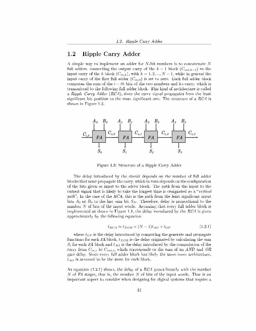
A simple way to implement an adder for N -bit numbers is to concatenate Nfull adders, connecting the output carry of the k − 1 block (Cout,k−1) to theinput carry of the k block (Cin,k), with k = 1, 2, ..., N − 1, while in general theinput carry of the �rst full adder (Cin,0) is set to zero. Each full adder blockcomputes the sum of the i− th bits of the two numbers and its carry, which istransmitted to the following full adder block. This kind of architecture is calleda Ripple Carry Adder (RCA), since the carry signal propagates from the leastsigni�cant bit position to the most signi�cant one. The structure of a RCA isshown in Figure 1.3.
Co,0 Co,1 Co,2 Co,3Ci,0
A0 B0
S0
FA
A1 B1
S1
FA
A2 B2
S2
FA
A3 B3
S3
FA
Figure 1.3: Structure of a Ripple Carry Adder
The delay introduced by the circuit depends on the number of full adderblocks that must propagate the carry, which in turn depends on the con�gurationof the bits given as input to the adder block. The path from the input to theoutput signal that is likely to take the longest time is designated as a �criticalpath�. In the case of the RCA, this is the path from the least signi�cant inputbits A0 or B0 to the last sum bit SN . Therefore, delay is proportional to thenumber N of bits of the input words. Assuming that every full adder block isimplemented as shown in Figure 1.1, the delay introduced by the RCA is givenapproximately by the following equation:
tRCA ≈ tXOR + (N − 1)tAO + tGP (1.2.1)
where tGP is the delay introduced by computing the generate and propagatefunctions for each FA block, tXOR is the delay originated by calculating the sumSi for each FA block and tAO is the delay introduced by the computation of thecarry from Cin,i to Cout,i, which corresponds to the sum of an AND and ORgate delay. Since every full adder block has likely the same inner architecture,tAO is assumed to be the same for each block.
As equation (1.2.1) shows, the delay of a RCA grows linearly with the numberN of FA stages, that is, the number N of bits of the input words. That is animportant aspect to consider when designing for digital systems that require a
12
1.3. Carry Lookahead Adder
sum of large number of bits. In particular, it is customary to avoid the use ofRCA topology for adders that compute operations involving 16 binary digitsor more, even though the area occupation is much smaller than other moreperforming adders that will be introduced in the following paragraphs.
1.3 Carry Lookahead Adder
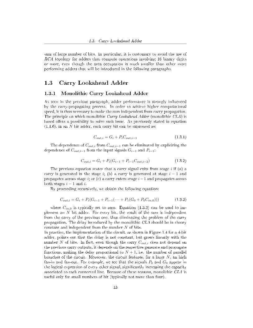
1.3.1 Monolithic Carry Lookahead Adder
As seen in the previous paragraph, adder performance is strongly in�uencedby the carry-propagating process. In order to achieve higher computationalspeed, it is thus necessary to make the sum independent from carry propagation.The principle on which monolithic Carry Lookahead Adder (monolithic CLA) isbased o�ers a possibility to solve such issue. As previously stated in equation(1.1.6), in an N bit adder, each carry bit can be expressed as:
Cout,i = Gi + PiCout,i−1 (1.3.1)
The dependence of Cout,i from Cout,i−1 can be eliminated by expliciting thedependence of Cout,i−1 from the input signals Gi−1 and Pi−1:
Cout,i = Gi + Pi(Gi−1 + Pi−1Cout,i−2) (1.3.2)
The previous equation states that a carry signal exits from stage i if (a) acarry is generated in the stage i; (b) a carry is generated at stage i − 1 andpropagates across stage i; or (c) a carry enters stage i−1 and propagates acrossboth stages i− 1 and i.
By proceeding recursively, we obtain the following equation:
Cout,i = Gi + Pi(Gi−1 + Pi−1(· · ·+ P1(G0 + P0Cin,0))) (1.3.3)
where Cin,0 is typically set to zero. Equation (1.3.3) can be used to im-plement an N bit adder. For every bit, the result of the sum is independentfrom the carry of the previous one, thus eliminating the problem of the carrypropagation. The delay introduced by the monolithic CLA should be in theoryconstant and independent from the number N of bits.In practice, the implementation of the circuit, as shown in Figure 1.4 for a 4-bitadder, points out that the delay is not constant, but grows linearly with thenumber N of bits. In fact, even though the carry Cout,i does not depend onthe previous carry outputs, it depends on the respective generate and propagatefunctions, making the delay proportional to N + 1, i.e. the number of parallelbranches of the circuit. Moreover, the circuit features, for a large N , an highfan-in and fan-out. For example, we see that the signals P0 and G0 appear inthe logical expression of every other signal, signi�cantly increasing the capacityassociated to each connected line. Because of these reasons, monolithic CLA isuseful only for small numbers of bit (typically not more than four).
13
1.3. Carry Lookahead Adder
G0
G1
G2
G3
P0
P1
P2
P3
Ci,0
Co,3
VDD
Figure 1.4: CMOS implementation of a 4-bit Monolithic Carry Lookahead Adder
1.3.2 Logarithmic Carry Lookahead Adder
The performance of monolithic CLA makes it suitable only for adding smallgroups of bits. In order to enhance the performance of the CLA it is neces-sary to modify the architecture of the adder by reorganizing it in a hierarchicalstructure, as in Logarithmic Carry Lookahead Adder (commonly referred to asCLA since its monolithic version is not particularly e�cient).CLA uses generation and propagation modules for each bit position and looka-head modules which are used to generate carry signals independently for a groupof k-bits. In addition to carry signal for the group, lookahead modules producegroup carry generate and group carry propagate outputs that indicate that thecarry is generated within the group, or that in incoming carry would propagateacross the group. In this way, it is possible to know more in advance whethercarry is generated or propagated inside a large group of bits, decreasing the de-lay due to the carry computation. Such modules are implemented by extendingequation (1.3.2) for a group of k-bits (for reasons that will shortly be explained,the index i is zero or an integer multiple of four):
Cout,i = Gi + PiCin,i
Cout,i+1 = Gi+1 + Pi+1Cout,i
Cout,i+2 = Gi+2 + Pi+2Cout,i+1
Cout,i+3 = Gi+3 + Pi+3Cout,i+2
(1.3.4)
14
1.3. Carry Lookahead Adder
Substituting Cout,i into Cout,i+1, then Cout,i+1 into Cout,i+2, then Cout,i+2 intoCout,i+3 yields the expanded equations:
Cout,i = Gi + PiCin,i
Cout,i+1 = Gi+1 + Pi+1Gi + Pi+1PiCin,i
Cout,i+2 = Gi+2 + Pi+2Gi+1 + Pi+2Pi+1Gi + Pi+2Pi+1PiCin,i
Cout,i+3 =Gi+3 + Pi+3Gi+2 + Pi+3Pi+2Gi+1 + Pi+3Pi+2Pi+1Gi
+ Pi+3Pi+2Pi+1PiCin,i
(1.3.5)
As seen in the previous paragraph, each additional stage increases the sizeof the logic gates in terms of number of inputs. Therefore, it is not appropriateto create a group that calculates the carry for a large number of bits. Themaximum number of inputs per gate for current technologies is four. In orderto continue the process, CLA collects carry, generate and propagate signals intolookahead modules that compute group-generate and group-propagate signals,respectively Gi+3:i and Pi+3:i (where i is zero or an integer multiple of four),over a four-bit group. Every lookahead module is able to anticipate whether acarry entering the module will be propagated all the way across it or generatedwithin it four times faster than a normal ripple process. Gi+3:i and Pi+3:i aredescribed by the following equation:
Gi+3:i = Gi+3 + Pi+3Gi+2 + Pi+3Pi+2Gi+1 + Pi+3Pi+2Pi+1Gi
Pi+3:i = Pi+3Pi+2Pi+1Pi
(1.3.6)
The notations Gj:i and Pj:i denote respectively group-generate and group-propagate for the group that includes bit positions from i-th to j-th. Thecarry equation can be expressed in terms of the 4-bit group-generate and group-propagate signals:
Cout,i+3:i = Gi+3:i + Pi+3:iCin,i+3:i (1.3.7)
where Cin,i+3:i is the input carry of the i-th stage. Usually, carry input for the�rst block is set to zero. The extended expressions of the carry equations canbe obtained by substitution as done for equation (1.3.4).In a recursive fashion, from group generate, propagate and carry, it is possibleto create a �group of groups" or �super group". The inputs of the �super group"are Gi+3:i and Pi+3:i signals computed by all the groups within it. Each �supergroup" produces propagate P ∗
j:i and generate G∗j:i signals that indicate that the
carry signal will be propagated across all the groups belonging to the �supergroup" or will be generated in one of them. Similarly to the group, a �super
15
1.3. Carry Lookahead Adder
group" produces an output carry signal as well as an input carry signal for eachof the groups in the level above:
G∗j:i = Gi+3:i + Pi+3:iGi+2:i + Pi+3:iPi+2:iGi+1:i + Pi+3:iPi+2:iPi+1:Gi:i
P ∗j:i = Pi+3:iPi+2:iPi+1:iPi:i
Cout,j = G∗j:i + P ∗
j:iCin,i
(1.3.8)
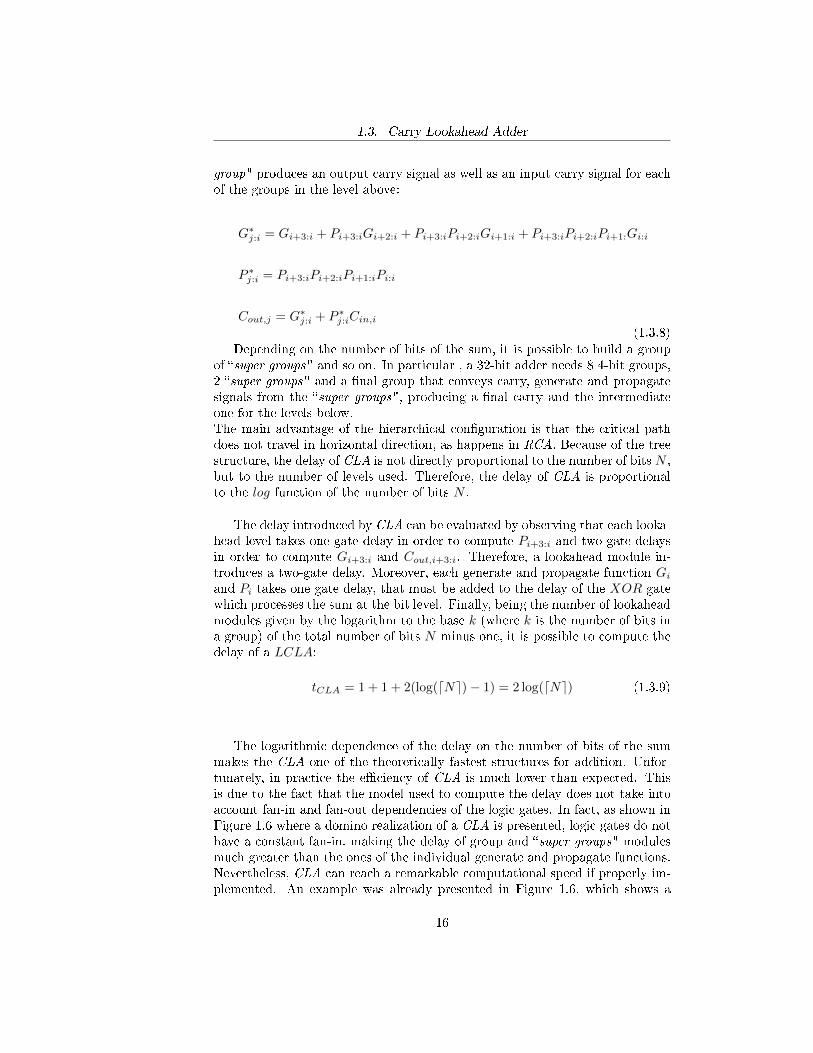
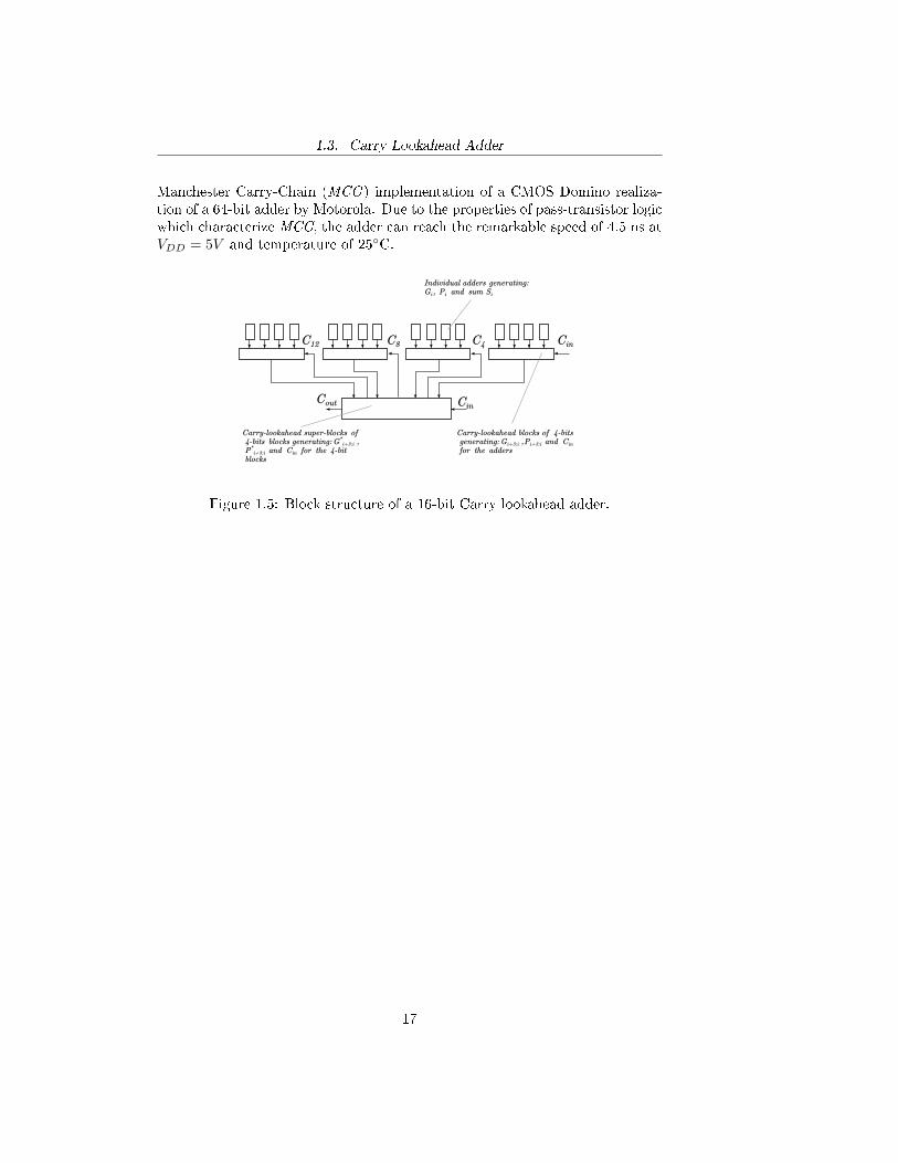
Depending on the number of bits of the sum, it is possible to build a groupof �super groups" and so on. In particular , a 32-bit adder needs 8 4-bit groups,2 �super groups" and a �nal group that conveys carry, generate and propagatesignals from the �super groups", producing a �nal carry and the intermediateone for the levels below.The main advantage of the hierarchical con�guration is that the critical pathdoes not travel in horizontal direction, as happens in RCA. Because of the treestructure, the delay of CLA is not directly proportional to the number of bits N ,but to the number of levels used. Therefore, the delay of CLA is proportionalto the log function of the number of bits N .
The delay introduced by CLA can be evaluated by observing that each looka-head level takes one gate delay in order to compute Pi+3:i and two gate delaysin order to compute Gi+3:i and Cout,i+3:i. Therefore, a lookahead module in-troduces a two-gate delay. Moreover, each generate and propagate function Gi
and Pi takes one gate delay, that must be added to the delay of the XOR gatewhich processes the sum at the bit level. Finally, being the number of lookaheadmodules given by the logarithm to the base k (where k is the number of bits ina group) of the total number of bits N minus one, it is possible to compute thedelay of a LCLA:
tCLA = 1 + 1 + 2(log(dNe)− 1) = 2 log(dNe) (1.3.9)
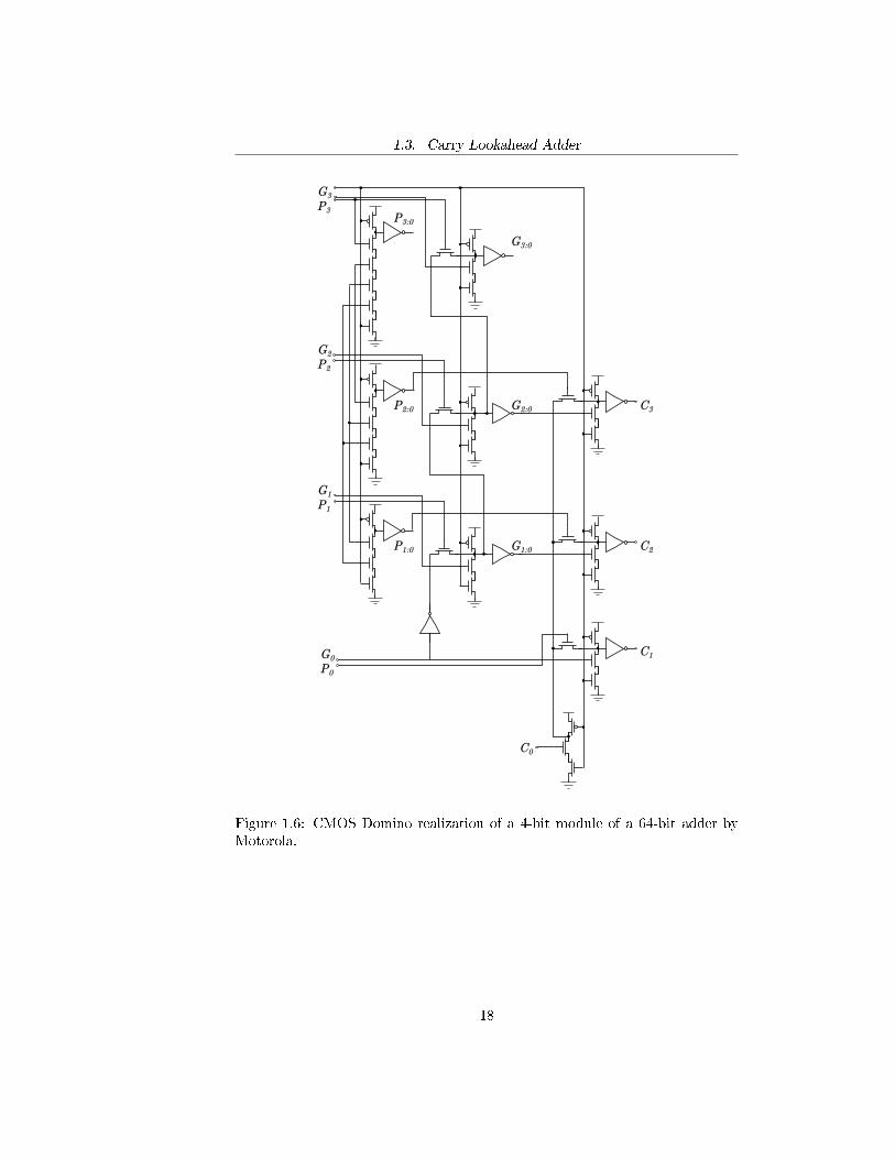
The logarithmic dependence of the delay on the number of bits of the summakes the CLA one of the theoretically fastest structures for addition. Unfor-tunately, in practice the e�ciency of CLA is much lower than expected. Thisis due to the fact that the model used to compute the delay does not take intoaccount fan-in and fan-out dependencies of the logic gates. In fact, as shown inFigure 1.6 where a domino realization of a CLA is presented, logic gates do nothave a constant fan-in, making the delay of group and �super groups" modulesmuch greater than the ones of the individual generate and propagate functions.Nevertheless, CLA can reach a remarkable computational speed if properly im-plemented. An example was already presented in Figure 1.6, which shows a
16
1.3. Carry Lookahead Adder
Manchester Carry-Chain (MCC ) implementation of a CMOS Domino realiza-tion of a 64-bit adder by Motorola. Due to the properties of pass-transistor logicwhich characterize MCC, the adder can reach the remarkable speed of 4.5 ns atVDD = 5V and temperature of 25◦C.
Cin
C4C8C12
Cout
Cin
Individual adders generating:Gi Pi and sum Si,
Carry-lookahead blocks of 4-bitsCin
for the addersgenerating:Gi+3:i Pi+3:i, and
super-blocksblocks G*
i+3:i
P*i+3:i
Carry-lookahead of4-bits generating: ,
and Cin for the 4-bitblocks
Figure 1.5: Block structure of a 16-bit Carry lookahead adder.
17
1.3. Carry Lookahead Adder
C0
P3:0
P2:0
P1:0
G3:0
G2:0
G1:0
C1
C2
C3
G3
P3
G2
P2
G1
P1
G0
P0
Figure 1.6: CMOS Domino realization of a 4-bit module of a 64-bit adder byMotorola.
18
1.4. Recurrence Solver Adders
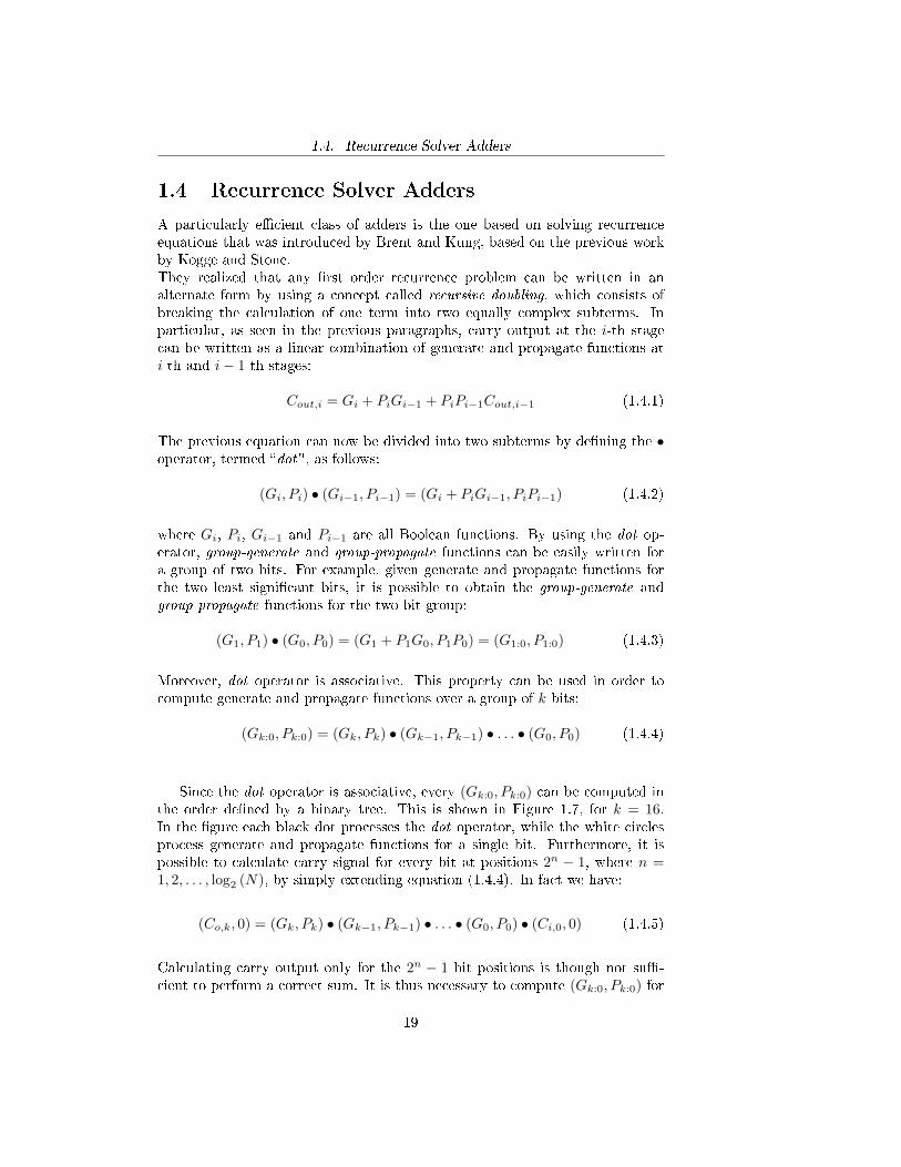
1.4 Recurrence Solver Adders
A particularly e�cient class of adders is the one based on solving recurrenceequations that was introduced by Brent and Kung, based on the previous workby Kogge and Stone.They realized that any �rst order recurrence problem can be written in analternate form by using a concept called recursive doubling, which consists ofbreaking the calculation of one term into two equally complex subterms. Inparticular, as seen in the previous paragraphs, carry output at the i-th stagecan be written as a linear combination of generate and propagate functions ati-th and i− 1-th stages:
Cout,i = Gi + PiGi−1 + PiPi−1Cout,i−1 (1.4.1)
The previous equation can now be divided into two subterms by de�ning the •operator, termed �dot", as follows:
(Gi, Pi) • (Gi−1, Pi−1) = (Gi + PiGi−1, PiPi−1) (1.4.2)
where Gi, Pi, Gi−1 and Pi−1 are all Boolean functions. By using the dot op-erator, group-generate and group-propagate functions can be easily written fora group of two bits. For example, given generate and propagate functions forthe two least signi�cant bits, it is possible to obtain the group-generate andgroup-propagate functions for the two-bit group:
(G1, P1) • (G0, P0) = (G1 + P1G0, P1P0) = (G1:0, P1:0) (1.4.3)
Moreover, dot operator is associative. This property can be used in order tocompute generate and propagate functions over a group of k bits:
(Gk:0, Pk:0) = (Gk, Pk) • (Gk−1, Pk−1) • . . . • (G0, P0) (1.4.4)
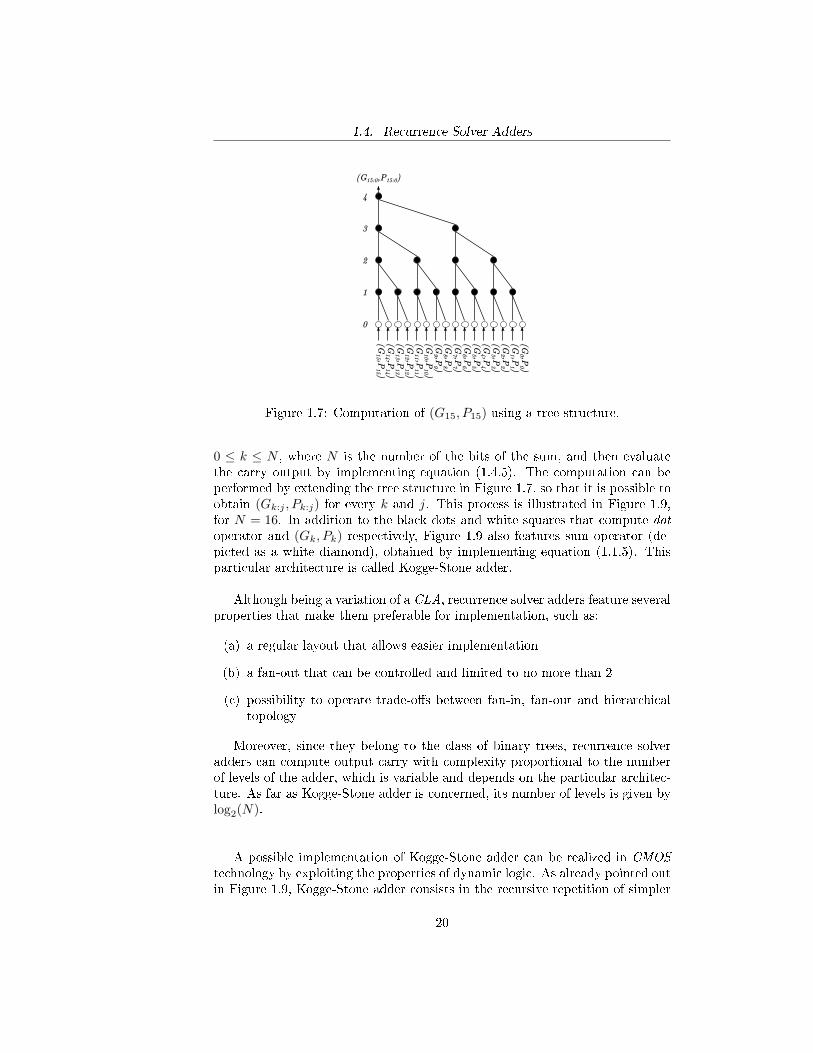
Since the dot operator is associative, every (Gk:0, Pk:0) can be computed inthe order de�ned by a binary tree. This is shown in Figure 1.7, for k = 16.In the �gure each black dot processes the dot operator, while the white circlesprocess generate and propagate functions for a single bit. Furthermore, it ispossible to calculate carry signal for every bit at positions 2n − 1, where n =1, 2, . . . , log2 (N), by simply extending equation (1.4.4). In fact we have:
(Co,k, 0) = (Gk, Pk) • (Gk−1, Pk−1) • . . . • (G0, P0) • (Ci,0, 0) (1.4.5)
Calculating carry output only for the 2n − 1 bit positions is though not su�-cient to perform a correct sum. It is thus necessary to compute (Gk:0, Pk:0) for
19
1.4. Recurrence Solver Adders
(G0 ,P
0 )(G
1 ,P1 )
(G2 ,P
2 )(G
3 ,P3 )
(G4 ,P
4 )(G
5 ,P5 )
(G6 ,P
6 )
(G8 ,P
8 )(G
9 ,P9 )
(G10 ,P
10 )
(G13 ,P
13 )
(G11 ,P
11 )
(G12 ,P
12 )
(G14 ,P
14 )
(G15 ,P
15 )
(G7 ,P
7 )
(G15:0,P15:0)
1
2
3
4
0
Figure 1.7: Computation of (G15, P15) using a tree structure.
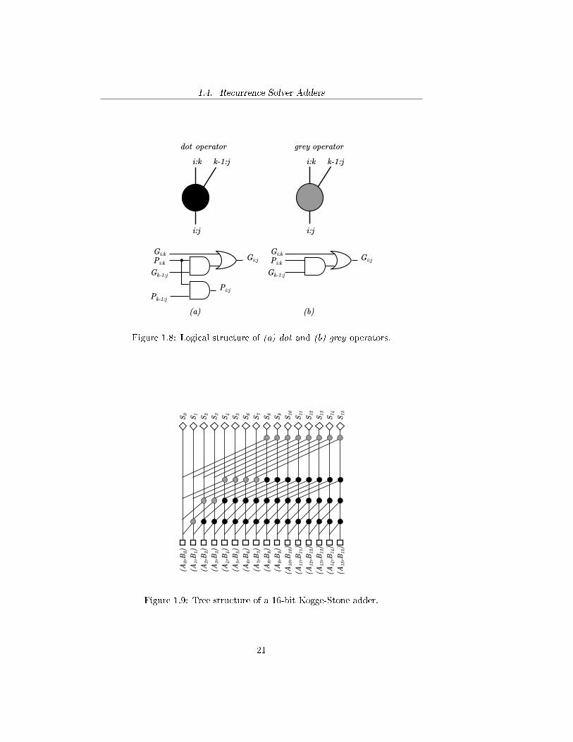
0 ≤ k ≤ N , where N is the number of the bits of the sum, and then evaluatethe carry output by implementing equation (1.4.5). The computation can beperformed by extending the tree structure in Figure 1.7, so that it is possible toobtain (Gk:j , Pk:j) for every k and j. This process is illustrated in Figure 1.9,for N = 16. In addition to the black dots and white squares that compute dotoperator and (Gk, Pk) respectively, Figure 1.9 also features sum operator (de-picted as a white diamond), obtained by implementing equation (1.1.5). Thisparticular architecture is called Kogge-Stone adder.
Although being a variation of a CLA, recurrence solver adders feature severalproperties that make them preferable for implementation, such as:
(a) a regular layout that allows easier implementation
(b) a fan-out that can be controlled and limited to no more than 2
(c) possibility to operate trade-o�s between fan-in, fan-out and hierarchicaltopology
Moreover, since they belong to the class of binary trees, recurrence solveradders can compute output carry with complexity proportional to the numberof levels of the adder, which is variable and depends on the particular architec-ture. As far as Kogge-Stone adder is concerned, its number of levels is given bylog2(N).
A possible implementation of Kogge-Stone adder can be realized in CMOStechnology by exploiting the properties of dynamic logic. As already pointed outin Figure 1.9, Kogge-Stone adder consists in the recursive repetition of simpler
20
1.4. Recurrence Solver Adders
Gi:k
Pi:k
Gk-1:j
Pk-1:j
Gi:j
Pi:j
Gi:k
Pi:k
Gk-1:j
Gi:j
i:k k-1:j
i:j
i:k k-1:j
i:j
dot operator grey operator
(a) (b)
Figure 1.8: Logical structure of (a) dot and (b) grey operators.
(A0,B
0)
(A1,B
1)
(A2,B
2)
(A3,B
3)
(A4,B
4)
(A5,B
5)
(A6,B
6)
(A7,B
7)
(A8,B
8)
(A9,B
9)
(A10,B
10)
(A11,B
11)
(A12,B
12)
(A13,B
13)
(A14,B
14)
(A15,B
15)
S0
S1
S2
S3
S4
S5
S6
S7
S8
S9
S10
S11
S12
S13
S14
S15
Figure 1.9: Tree structure of a 16-bit Kogge-Stone adder.
21
1.4. Recurrence Solver Adders
CLK
CLK
VDDVDD
CLK
CLK
Ai
Bi
Pi Gi
Ai Bi
(a) (b)
Figure 1.10: CMOS Domino implementation of (a) propagate and (b) generatesignals.
Pi:i-k+1
Pi-k:i-2k+1
CLK
CLK
VDD
Pi:i-2k+1
(a)
VDD
CLK
CLK
Pi:i-k+1
Gi-k:i-2k+1
Gi:i-k+1
Gi:i-2k+1
(b)
Figure 1.11: CMOS Domino implementation of the dot operator: (a) group-propagate and (b) group-generate signals.
22
1.4. Recurrence Solver Adders
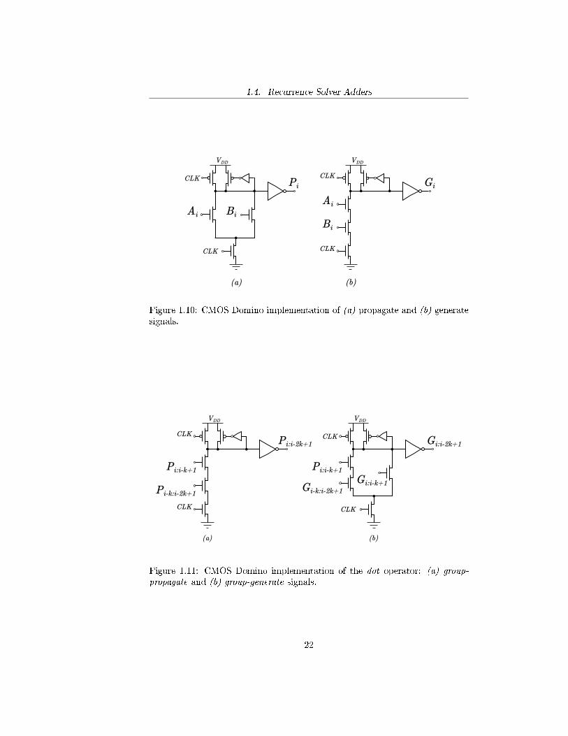
modules, which realize dot operator, generate, propagate and sum functions.The Domino CMOS implementation of generate and propagate functions fromequations (1.1.3) and (1.1.4) is shown in Figure 1.10. Note that propagatefunction does not actually implement a XOR gate, but the following equation:
Pi = Ai +Bi (1.4.6)
which represents a OR gate. This is an alternate de�nition of the propagatefunction that allows carry to be forwarded also when both Ai and Bi assumelogical value 1. Due to the way generate and propagate bits are used by CLAand recurrence solver adders, propagate de�nition given by equation (1.4.6) isequivalent to the one given by equation (1.1.4) 1. Because of this, propagatefunction can be easily implemented in Domino logic. In addition, both generateand propagate functions feature a bleeder circuit whose function is to eliminateevery static power consumption originated by the pull-down network. Everybleeder p-MOS has a small inverter connected to its gate in order to decoupleit from the output load, allowing a fast switching o�.Figure 1.11 shows the Domino logic implementation of the dot operator. Inorder to implement equation (1.4.2), every dot operator consists of two modules:the �rst computes group-propagate and the second group-generate. The inputsof group-propagate modules are given by the signals Pi:i−k+1 and Pi−k:i−2k+1,where i represents the bit position of the operand and k represents the logiclevel from which the input is produced. Similarly for group-generate the imputsare Gi−k:i−2k+1, Gi:i−k+1 and Pi:i−k+1. The outputs of the two modules willbe Pi:i−2k+1 and Gi:i−2k+1 respectively. In addition, since group-propagate andgroup-generate functions do not represent the �rst stage of the circuit, it wouldbe possible remove the evaluation transistor from the PDN in order to reduce thelogical e�ort from 1 to 2/3. Note that by doing this it would also be necessary todelay the clock signal of stage k from the one of stage k−1 in order to eliminatethe direct path from VDD to ground. In this way the clock signal is delayed bya constant time from a stage and the following one.After computing all generate and propagate functions it is also necessary tocalculate the sum of the i-th bit of the two operands by implementing thefollowing equation:
Si = Ai ⊕Bi (1.4.7)
A static implementation of equation (1.4.7) is not particularly e�cient, hav-ing implemented the previous stages in Domino logic. In fact a static gate couldincrease the delay of the circuit and cause unwanted transitions whether thefollowing stage is implemented in dynamic logic. A possible way to computethe sum using Domino logic is to precompute the two possible outputs for Si,S0i = Ai ⊕Bi and S1
i = Ai ⊕ Bi, and select the proper output by exploiting
1Note that equations (1.4.6) and (1.1.4) are not equivalent for full-adders or RCA.
23
1.4. Recurrence Solver Adders
Gi:0
Si0
Si1
S
CLKD
Gi:0
VDD VDD VDD
CLK
CLK
CLK
CLK
CLKD
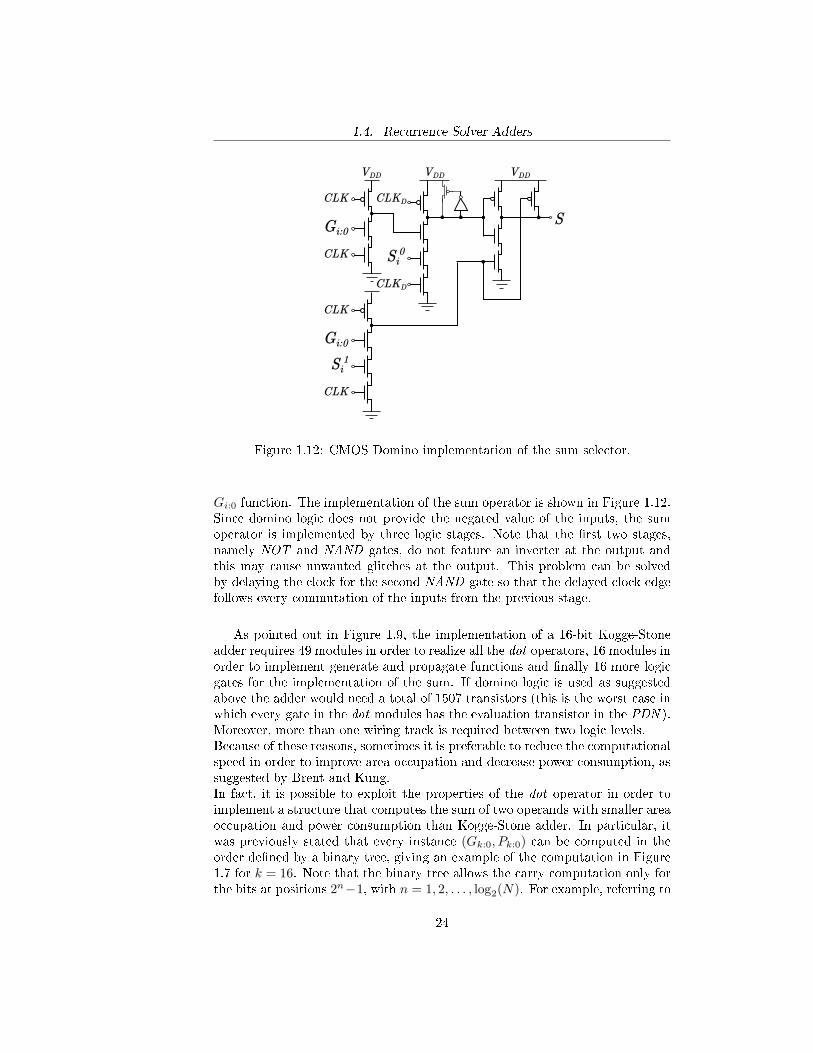
Figure 1.12: CMOS Domino implementation of the sum selector.
Gi:0 function. The implementation of the sum operator is shown in Figure 1.12.Since domino logic does not provide the negated value of the inputs, the sumoperator is implemented by three logic stages. Note that the �rst two stages,namely NOT and NAND gates, do not feature an inverter at the output andthis may cause unwanted glitches at the output. This problem can be solvedby delaying the clock for the second NAND gate so that the delayed clock edgefollows every commutation of the inputs from the previous stage.
As pointed out in Figure 1.9, the implementation of a 16-bit Kogge-Stoneadder requires 49 modules in order to realize all the dot operators, 16 modules inorder to implement generate and propagate functions and �nally 16 more logicgates for the implementation of the sum. If domino logic is used as suggestedabove the adder would need a total of 1507 transistors (this is the worst case inwhich every gate in the dot modules has the evaluation transistor in the PDN ).Moreover, more than one wiring track is required between two logic levels.Because of these reasons, sometimes it is preferable to reduce the computationalspeed in order to improve area occupation and decrease power consumption, assuggested by Brent and Kung.In fact, it is possible to exploit the properties of the dot operator in order toimplement a structure that computes the sum of two operands with smaller areaoccupation and power consumption than Kogge-Stone adder. In particular, itwas previously stated that every instance (Gk:0, Pk:0) can be computed in theorder de�ned by a binary tree, giving an example of the computation in Figure1.7 for k = 16. Note that the binary tree allows the carry computation only forthe bits at positions 2n−1, with n = 1, 2, . . . , log2(N). For example, referring to
24
1.4. Recurrence Solver Adders
(A0,B
0)
(A1,B
1)
(A2,B
2)
(A3,B
3)
(A4,B
4)
(A5,B
5)
(A6,B
6)
(A7,B
7)
(A8,B
8)
(A9,B
9)
(A10,B
10)
(A11,B
11)
(A12,B
12)
(A13,B
13)
(A14,B
14)
(A15,B
15)
S0
S1
S2
S3
S4
S5
S6
S7
S8
S9
S10
S11
S12
S13
S14
S15
Figure 1.13: Tree structure of a 16-bit Brent-Kung adder.
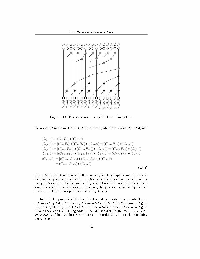
the structure in Figure 1.7, it is possible to compute the following carry outputs:
(Co,0, 0) = (G0, P0) • (Ci,0, 0)
(Co,1, 0) = [(G1, P1) • (G0, P0)] • (Ci,0, 0) = (G1:0, P1:0) • (Ci,0, 0)
(Co,3, 0) = [(G3:2, P3:2) • (G1:0, P1:0)] • (Ci,0, 0) = (G3:0, P3:0) • (Ci,0, 0)
(Co,7, 0) = [(G7:4, P7:4) • (G3:0, P3:0)] • (Ci,0, 0) = (G7:0, P7:0) • (Ci,0, 0)
(Co,15, 0) = [(G15:8, P15:8) • (G7:0, P7:0)] • (Ci,0, 0)
= (G15:0, P15:0) • (Ci,0, 0)(1.4.8)
Since binary tree itself does not allow to compute the complete sum, it is neces-sary to juxtapose another structure to it so that the carry can be calculated forevery position of the two operands. Kogge and Stone's solution to this problemwas to reproduce the tree structure for every bit position, signi�cantly increas-ing the number of dot operators and wiring tracks.
Instead of reproducing the tree structure, it is possible to compute the re-maining carry outputs by simply adding a second tree to the structure in Figure1.7, as suggested by Brent and Kung. The resulting scheme shown in Figure1.13 is known as Brent-Kung adder. The additional structure, called inverse bi-nary tree, combines the intermediate results in order to compute the remainingcarry outputs.
25
1.4. Recurrence Solver Adders
In this way, the number of dot operators implemented in the adder is signif-icantly reduced: referring to a 16-bit adder, instead of the 49 requested by aKogge-Stone adder, a Brent-Kung adder only needs 27. Moreover the numberof wiring tracks between two logic levels is limited to one.Note that the inverse binary tree consists of a di�erent class of dot operators,depicted as grey dots in Figure 1.13. Since the implementation of the sum onlyrequires the group-generate signal Gi:0 in addition to the two possible values ofthe signal Si, grey operators implement only the following equation:
Gi:i−2k+1 = Gi:i−k+1 + Pi:i−k+1Gi:i−2k+1 (1.4.9)
instead of equation (1.4.2). Because of this, only three inputs are neededand only one output is produced. The implementation of the grey operatorcan be seen in Figure 1.11 b. Note that grey operators are also used in theimplementation of Kogge-Stone adder for the nodes directly connected to themodules that compute the sum.The width w of an adder can be de�ned as the number of bits it accepts atone time from each operand. For the parallel adders considered so far, w = Nwas assumed. For any Brent-Kung adder it can be proven that all the carriesin an N -bit addition can be computed in time proportional to (N/w) + log(w)and in area proportional to w log(w)+ 1, and so can the addition. The applica-tion of the previous bound to the case w = N leads to the conclusion that thecomputation delay for a N -bit Brent-Kung adder is proportional to log(N)+ 1.Nevertheless, Brent-Kung adder does not reach the computational speed of aKogge-Stone adder. This is due to the fact that the structure of the wiringtracks is less regularly distributed and the fan-out is variable for each logicgate. In particular, referring to the 16-bit adder in Figure 1.13, the fan-out ofthe node associated to the intermediate carry output (Co,7, 0) is given by �vedot operators and a sum function, signi�cantly increasing the delay.
26
1.5. Radix-4 implementation of adders
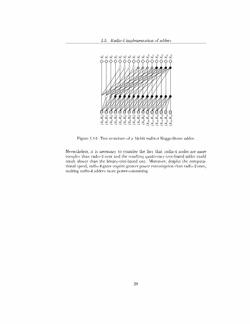
1.5 Radix-4 implementation of adders
Another factor that contributes to the enhancement of the delay is the num-ber of logic levels of the adder which, in the case of a recurrence solver adder,corresponds to the number of carries (or equivalently dot operators) grouped ineach step of the computation. This parameter is often referred to as the depthof the adder. Considering that in a recurrence solver adder all the dot operatorshave the same architecture and therefore the same delay, to a greater depthcorresponds greater delay. Moreover, a great number of subsequent logic gatessigni�cantly increases the fan-out associated to each bit of the operands.A possible way to reduce the depth of an adder is the implementation throughradix-4 architecture. All the recurrence solver adders analyzed so far were im-plemented by using radix-2 architecture, which means coupling two signals intoa dot operator so that it is possible to compute generate and propagate func-tions over a group of two bits. As the name suggests, radix-4 architecture groupsfour signals into a single dot operator, computing generate and propagate for agroup of four bits. It is thus possible to rede�ne equation (1.4.2) for a group offour bits as follows:
Dot4((Gi+3, Pi+3), (Gi+2, Pi+2), (Gi + 1, Pi+1), (Gi, Pi)
)=
(Gi+3 + Pi+3Gi+2 + Pi+3Pi+2Gi+1 + Pi+3Pi+2Pi+1Gi, Pi+3Pi+2Pi+1Pi)(1.5.1)
Consequently recurrence solver adders can be implemented by a quaternary treeinstead of a binary one. Figure 1.14 shows a 16-bit radix-4 Kogge-Stone adder.Note that in addition to the radix-4 dot operators the adder also features radix-2dot operators (depicted as a white circle) and radix-4 grey operators (depictedas a grey circle). The former implement equation (1.4.2) as for radix-2 adders,the latter implement the following equation:
Grey4
((Gi+2, Pi+2),(Gi + 1, Pi+1), (Gi, Pi)
)=
= (Gi+2 + Pi+2Gi+1 + Pi+2Pi+1Gi, Pi+2Pi+1Pi)(1.5.2)
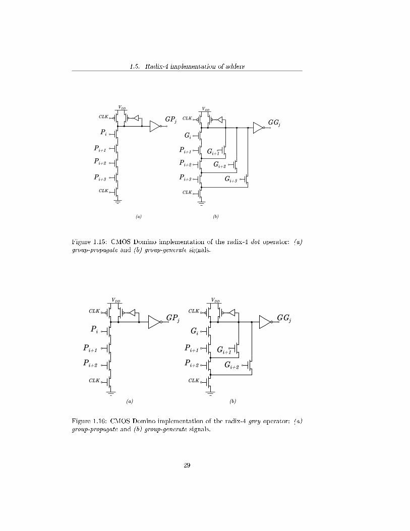
A possible implementation in CMOS Domino logic of radix-4 dot and greyoperators is shown in Figure 1.15 and Figure 1.16 respectively. As for the imple-mentation of the radix-2 dot operator presented in the previous paragraph, bothmodules feature a bleeder in order to eliminate every static power consumptionoriginated by the pull-down network.By applying radix-4 architecture it is possible to reduce the depth of the adderand therefore decrease the number of carries grouped in each step. For ex-ample, for a 16-bit Kogge-Stone adder, the depth decreases from four to two.
27
1.5. Radix-4 implementation of adders
(A0,B
0)
(A1,B
1)
(A2,B
2)
(A3,B
3)
(A4,B
4)
(A5,B
5)
(A6,B
6)
(A7,B
7)
(A8,B
8)
(A9,B
9)
(A10,B
10)
(A11,B
11)
(A12,B
12)
(A13,B
13)
(A14,B
14)
(A15,B
15)
S0
S1
S2
S3
S4
S5
S6
S7
S8
S9
S10
S11
S12
S13
S14
S15
Figure 1.14: Tree structure of a 16-bit radix-4 Kogge-Stone adder.
Nevertheless, it is necessary to consider the fact that radix-4 nodes are morecomplex than radix-2 ones and the resulting quaternary-tree-based adder couldresult slower than the binary-tree-based one. Moreover, despite the computa-tional speed, radix-4 gates require greater power consumption than radix-2 ones,making radix-4 adders more power-consuming.
28
1.5. Radix-4 implementation of adders
(a) (b)
CLK
CLK
VDD
Gi
Gi+1
Gi+2
Gi+3
Pi+1
Pi+2
Pi+3
GGj
CLK
CLK
VDD
Pi
Pi+1
Pi+2
Pi+3
GPj
Figure 1.15: CMOS Domino implementation of the radix-4 dot operator: (a)group-propagate and (b) group-generate signals.
(a) (b)
CLK
CLK
VDD
Gi
Gi+1
Gi+2
Pi+1
Pi+2
GGj
CLK
CLK
VDD
Pi
Pi+1
Pi+2
GPj
Figure 1.16: CMOS Domino implementation of the radix-4 grey operator: (a)group-propagate and (b) group-generate signals.
29
1.5. Radix-4 implementation of adders
30
Chapter 2
Design of a 32-bit High-Speed
Adder
Since adders occupy a critical position inside arithmetic logic units of micropro-cessors, it is very important to ensure that their performance adequately meetsgiven speci�cations on speed, power and area occupation. The optimization ofsuch speci�cations can be achieved at both logical and circuit level. The previ-ous chapter featured the analysis of the logical level, presenting many e�cienttopological solutions in order to implement high-speed adders. The purpose ofthe second part of this work is to verify the results presented in the previouschapter by implementing notable adder structures and verifying their perfor-mance through simulations.The adder topologies chosen for simulation are the following: 32-bit Kogge-Stoneradix-2 adder; 32-bit Brent-Kung radix-2 adder; 32-bit Kogge-Stone radix-4adder and 32-bit Brent-Kung radix-4 adder. Kogge-Stone topology was mainlychosen because it ensures high performance despite a considerable power con-sumption and area occupation, while Brent-Kung topology ensures lower com-putational speed but also lower area occupation and power consumption. More-over, a further comparison can be made between radix-2 and radix-4 architec-tures can be made in terms of overall computational speed and area occupation.Circuit simulation for veri�cation of performance was carried out by using Ca-dence Design Framework II R©, an electronic design automated software fordigital, analog and mixed circuits.
2.1 Circuit implementation
Because of its peculiar properties, for circuit implementation Dynamic Dominologic was chosen. In particular, since each operation is free from glitches aseach gate can make only one 0 → 1 transition in evaluation, Domino logic isparticularly apt to implement cascades of logic gates as the ones of recurrence
31
2.1. Circuit implementation
solver adders. Moreover, as all Dynamic logic does, the area occupation is muchsmaller and computational speed is much faster than the conventional CMOSlogic.Given the modular structure of recurrence solver adders, many circuit blocksare shared between di�erent adder topologies. For example dot operator is iden-tically implemented for both Kogge-Stone and Brent-Kung adders. Because ofthis reason, this paragraph will deal with each module separately before intro-ducing the proper adder topology. All the following blocks were implementedby using the 0.35µm CMOS C35 process.
2.1.1 Blocks implementation
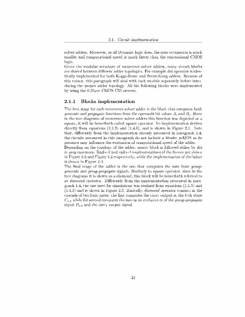
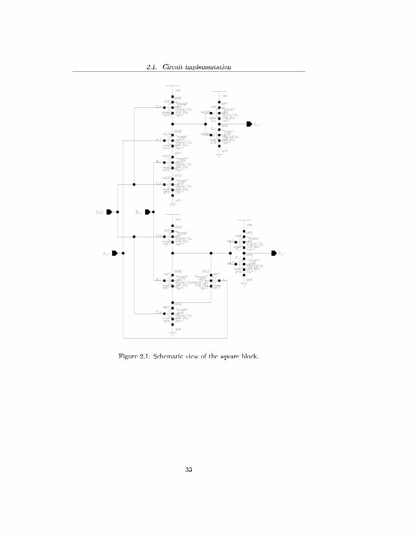
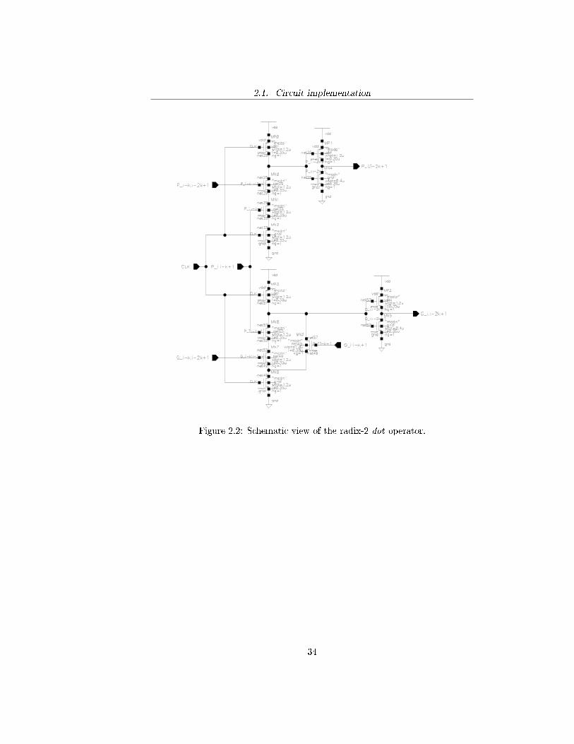
The �rst stage for each recurrence solver adder is the block that computes bothgenerate and propagate functions from the operands bit values Ai and Bi. Sincein the tree diagrams of recurrence solver adders this function was depicted as asquare, it will be henceforth called square operator. Its implementation derivesdirectly from equations (1.1.3) and (1.4.6), and is shown in Figure 2.1. Notethat, di�erently from the implementation already presented in paragraph 1.4,the circuits presented in this paragraph do not include a bleeder p-MOS as itspresence may in�uence the evaluation of computational speed of the adder.Depending on the topology of the adder, square block is followed either by dotor grey operators. Radix-2 and radix-4 implementations of the former are shownin Figure 2.2 and Figure 2.3 respectively; while the implementation of the latteris shown in Figure 2.4.The �nal stage of the adder is the one that computes the sum from group-generate and group-propagate signals. Similarly to square operator, since in thetree diagrams it is shown as a diamond, this block will be henceforth referred toas diamond operator. Di�erently from the implementation presented in para-graph 1.4, the one used for simulations was realized from equations (1.1.5) and(1.4.5) and is shown in Figure 2.5. Basically, diamond operator consists in thecascade of two logic gates: the �rst computes the carry output at the k-th stageCo,k while the second computes the sum as an exclusive or of the group-propagatesignal Pk:0 and the carry output signal.
32
2.1. Circuit implementation
Figure 2.1: Schematic view of the square block.
33
2.1. Circuit implementation
Figure 2.2: Schematic view of the radix-2 dot operator.
34
2.1. Circuit implementation
Figure 2.3: Schematic view of the radix-4 dot operator.
35
2.1. Circuit implementation
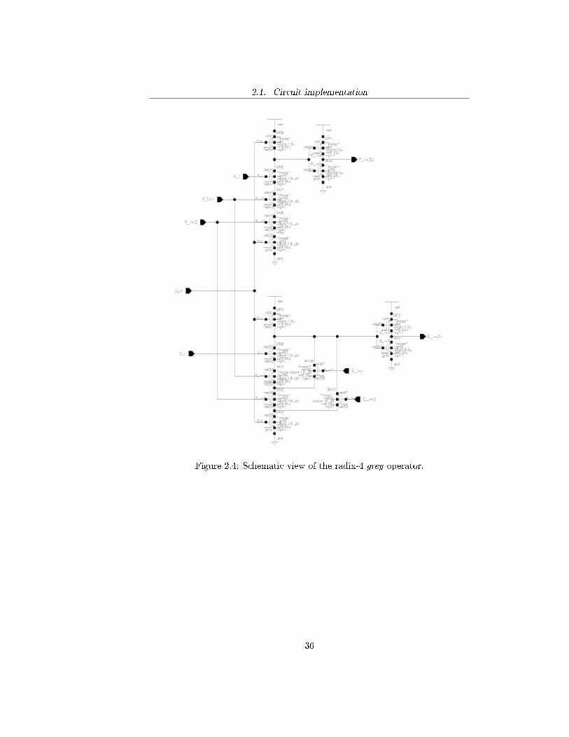
Figure 2.4: Schematic view of the radix-4 grey operator.
36
2.1. Circuit implementation
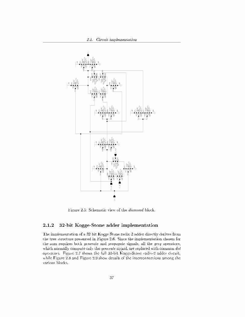
Figure 2.5: Schematic view of the diamond block.
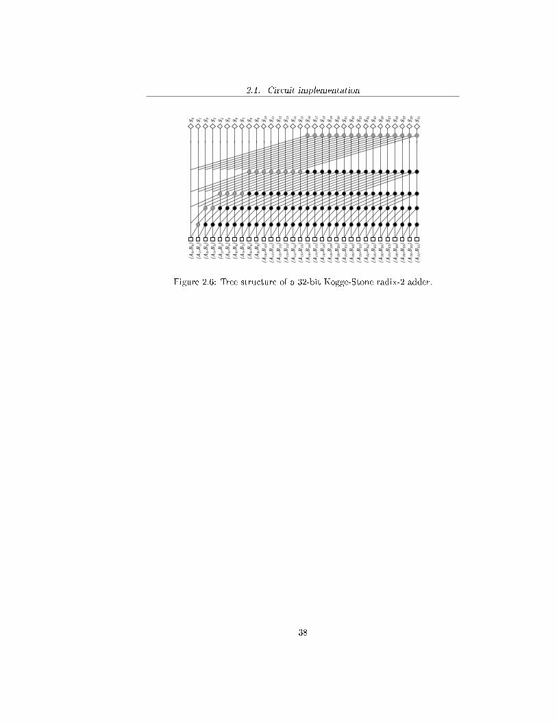
2.1.2 32-bit Kogge-Stone adder implementation
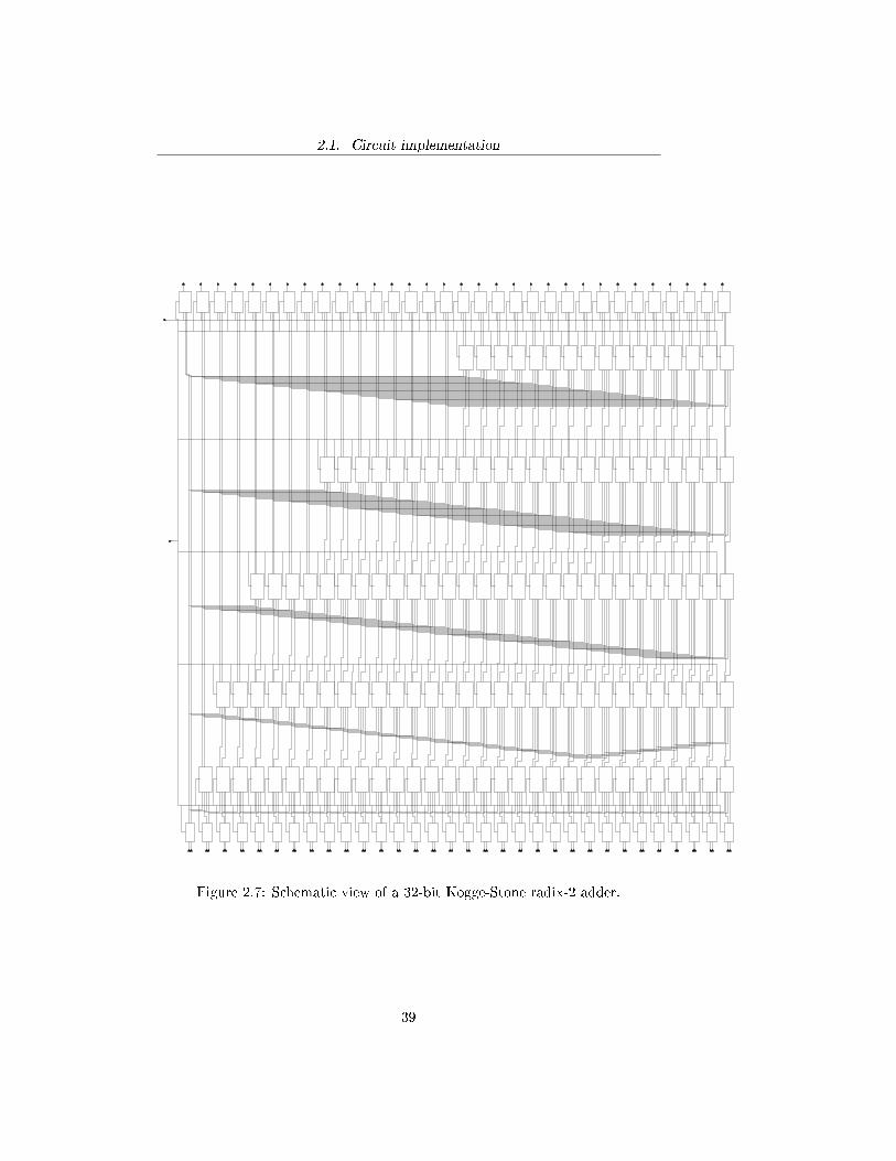
The implementation of a 32-bit Kogge-Stone radix-2 adder directly derives fromthe tree structure presented in Figure 2.6. Since the implementation chosen forthe sum requires both generate and propagate signals, all the grey operators,which normally compute only the generate signal, are replaced with common dotoperators. Figure 2.7 shows the full 32-bit Kogge-Stone radix-2 adder circuit,while Figure 2.8 and Figure 2.9 show details of the interconnections among thevarious blocks.
37
2.1. Circuit implementation
(A1,B
1)
(A2,B
2)
(A3,B
3)
(A4,B
4)
(A5,B
5)
(A6,B
6)
(A7,B
7)
(A8,B
8)
(A9,B
9)
(A10,B
10)
(A11,B
11)
(A12,B
12)
(A13,B
13)
(A14,B
14)
(A15,B
15)
S0
S1
S2
S3
S4
S5
S6
S7
S8
S9
S10
S11
S12
S13
S14
S15
(A16,B
16)
(A30,B
30)
(A17,B
17)
(A18,B
18)
(A19,B
19)
(A20,B
20)
(A21,B
21)
(A22,B
22)
(A23,B
23)
(A24,B
24)
(A25,B
25)
(A26,B
26)
(A27,B
27)
(A28,B
28)
(A29,B
29)
(A31,B
31)
(A0,B
0)
S16
S20
S30
S17
S18
S19
S21
S22
S23
S24
S25
S26
S27
S28
S29
S31
Figure 2.6: Tree structure of a 32-bit Kogge-Stone radix-2 adder.
38
2.1. Circuit implementation
Figure 2.7: Schematic view of a 32-bit Kogge-Stone radix-2 adder.
39
2.1. Circuit implementation
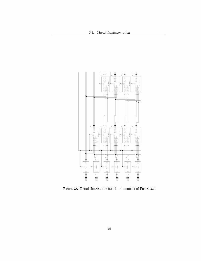
Figure 2.8: Detail showing the �rst four imputs of of Figure 2.7.
40
2.1. Circuit implementation
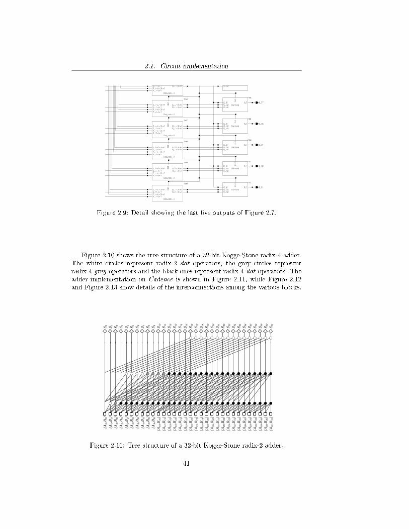
Figure 2.9: Detail showing the last �ve outputs of Figure 2.7.
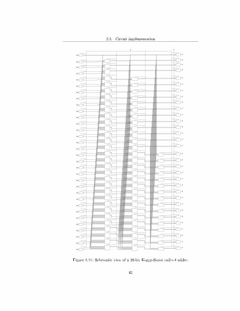
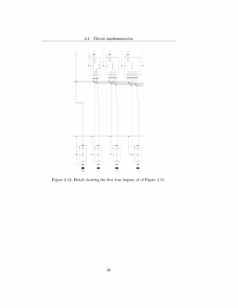
Figure 2.10 shows the tree structure of a 32-bit Kogge-Stone radix-4 adder.The white circles represent radix-2 dot operators, the grey circles representradix-4 grey operators and the black ones represent radix-4 dot operators. Theadder implementation on Cadence is shown in Figure 2.11, while Figure 2.12and Figure 2.13 show details of the interconnections among the various blocks.
(A1,B
1)
(A2,B
2)
(A3,B
3)
(A4,B
4)
(A5,B
5)
(A6,B
6)
(A7,B
7)
(A8,B
8)
(A9,B
9)
(A10,B
10)
(A11,B
11)
(A12,B
12)
(A13,B
13)
(A14,B
14)
(A15,B
15)
S0
S1
S2
S3
S4
S5
S6
S7
S8
S9
S10
S11
S12
S13
S14
S15
(A16,B
16)
(A30,B
30)
(A17,B
17)
(A18,B
18)
(A19,B
19)
(A20,B
20)
(A21,B
21)
(A22,B
22)
(A23,B
23)
(A24,B
24)
(A25,B
25)
(A26,B
26)
(A27,B
27)
(A28,B
28)
(A29,B
29)
(A31,B
31)
(A0,B
0)
S16
S20
S30
S17
S18
S19
S21
S22
S23
S24
S25
S26
S27
S28
S29
S31
Figure 2.10: Tree structure of a 32-bit Kogge-Stone radix-2 adder.
41
2.1. Circuit implementation
Figure 2.11: Schematic view of a 32-bit Kogge-Stone radix-4 adder.
42
2.1. Circuit implementation
Figure 2.12: Detail showing the �rst four imputs of of Figure 2.11.
43
2.1. Circuit implementation
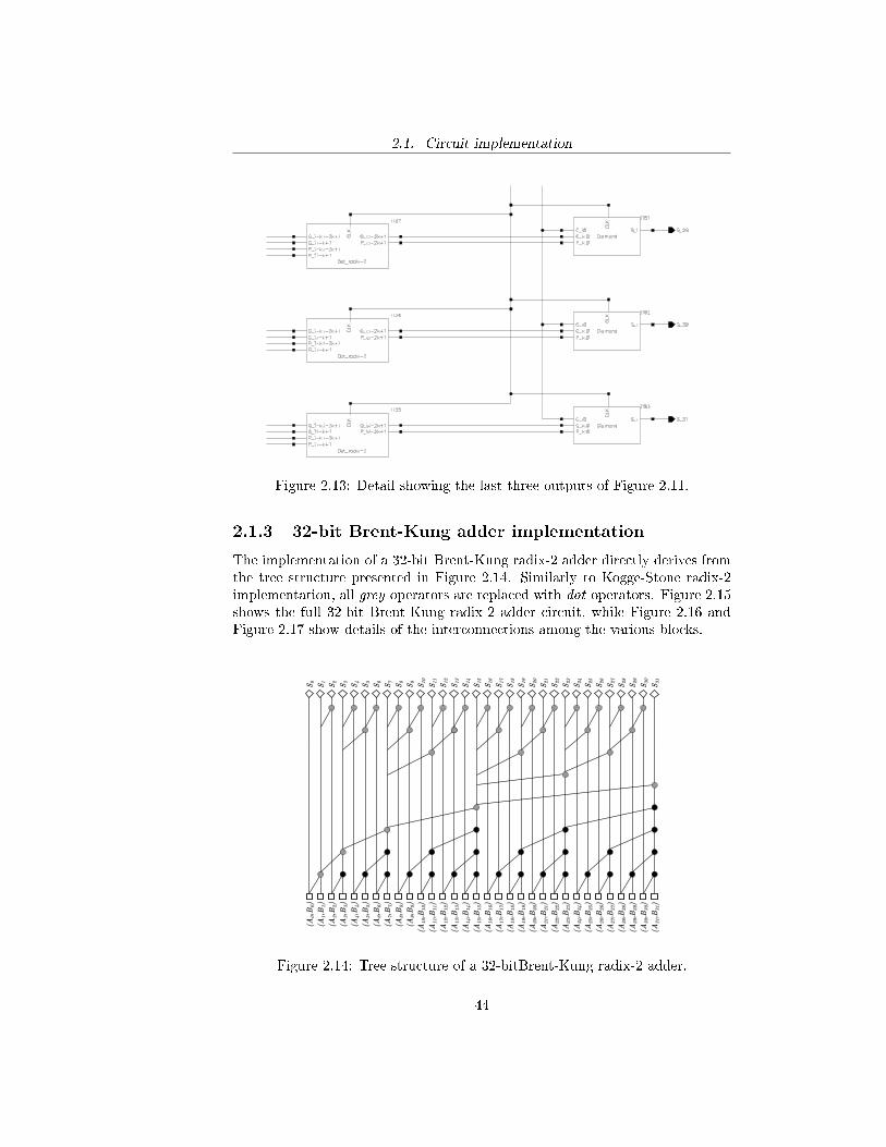
Figure 2.13: Detail showing the last three outputs of Figure 2.11.
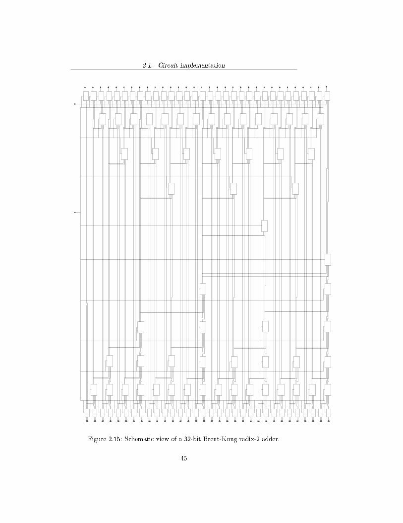
2.1.3 32-bit Brent-Kung adder implementation
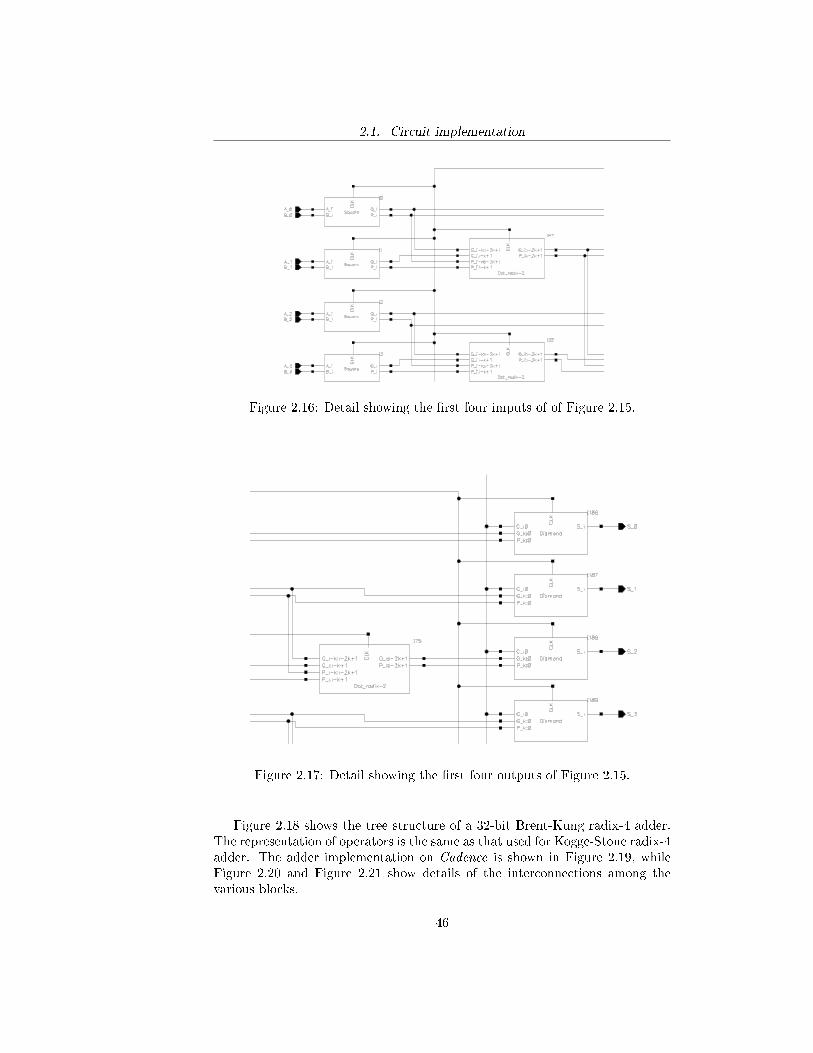
The implementation of a 32-bit Brent-Kung radix-2 adder directly derives fromthe tree structure presented in Figure 2.14. Similarly to Kogge-Stone radix-2implementation, all grey operators are replaced with dot operators. Figure 2.15shows the full 32-bit Brent-Kung radix-2 adder circuit, while Figure 2.16 andFigure 2.17 show details of the interconnections among the various blocks.
(A1,B
1)
(A2,B
2)
(A3,B
3)
(A4,B
4)
(A5,B
5)
(A6,B
6)
(A7,B
7)
(A8,B
8)
(A9,B
9)
(A10,B
10)
(A11,B
11)
(A12,B
12)
(A13,B
13)
(A14,B
14)
(A15,B
15)
S0
S1
S2
S3
S4
S5
S6
S7
S8
S9
S10
S11
S12
S13
S14
S15
(A16,B
16)
(A30,B
30)
(A17,B
17)
(A18,B
18)
(A19,B
19)
(A20,B
20)
(A21,B
21)
(A22,B
22)
(A23,B
23)
(A24,B
24)
(A25,B
25)
(A26,B
26)
(A27,B
27)
(A28,B
28)
(A29,B
29)
(A31,B
31)
(A0,B
0)
S16
S20
S30
S17
S18
S19
S21
S22
S23
S24
S25
S26
S27
S28
S29
S31
Figure 2.14: Tree structure of a 32-bitBrent-Kung radix-2 adder.
44
2.1. Circuit implementation
Figure 2.15: Schematic view of a 32-bit Brent-Kung radix-2 adder.
45
2.1. Circuit implementation
Figure 2.16: Detail showing the �rst four imputs of of Figure 2.15.
Figure 2.17: Detail showing the �rst four outputs of Figure 2.15.
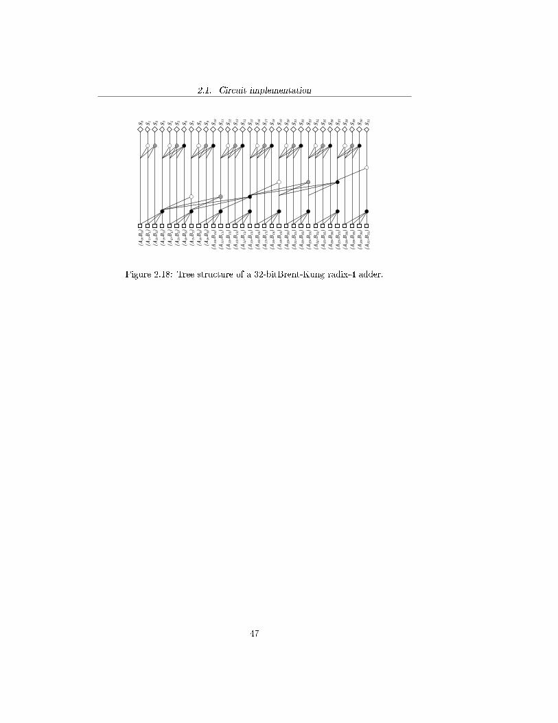
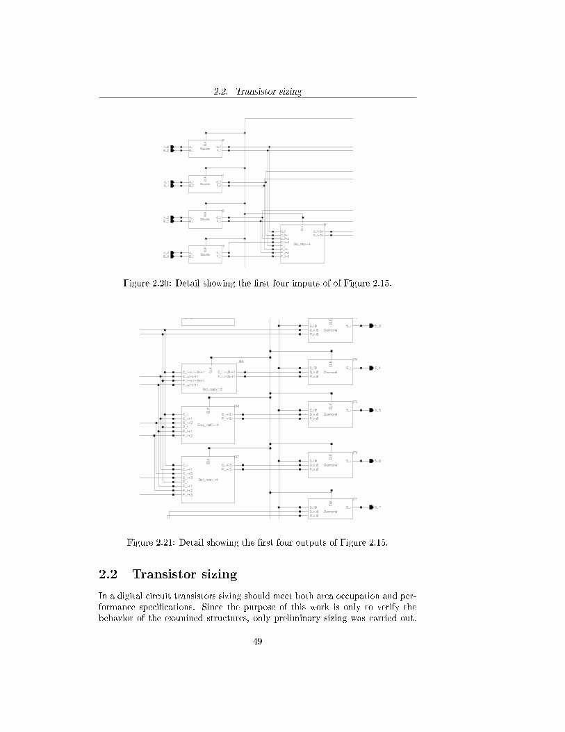
Figure 2.18 shows the tree structure of a 32-bit Brent-Kung radix-4 adder.The representation of operators is the same as that used for Kogge-Stone radix-4adder. The adder implementation on Cadence is shown in Figure 2.19, whileFigure 2.20 and Figure 2.21 show details of the interconnections among thevarious blocks.
46
2.1. Circuit implementation
(A1,B
1)
(A2,B
2)
(A3,B
3)
(A4,B
4)
(A5,B
5)
(A6,B
6)
(A7,B
7)
(A8,B
8)
(A9,B
9)
(A10,B
10)
(A11,B
11)
(A12,B
12)
(A13,B
13)
(A14,B
14)
(A15,B
15)
S0
S1
S2
S3
S4
S5
S6
S7
S8
S9
S10
S11
S12
S13
S14
S15
(A16,B
16)
(A30,B
30)
(A17,B
17)
(A18,B
18)
(A19,B
19)
(A20,B
20)
(A21,B
21)
(A22,B
22)
(A23,B
23)
(A24,B
24)
(A25,B
25)
(A26,B
26)
(A27,B
27)
(A28,B
28)
(A29,B
29)
(A31,B
31)
(A0,B
0)
S16
S20
S30
S17
S18
S19
S21
S22
S23
S24
S25
S26
S27
S28
S29
S31
Figure 2.18: Tree structure of a 32-bitBrent-Kung radix-4 adder.
47
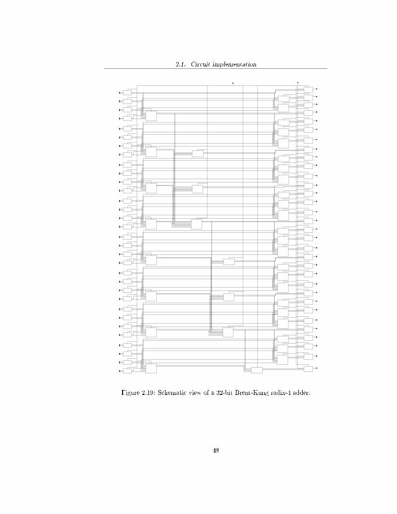
2.1. Circuit implementation
Figure 2.19: Schematic view of a 32-bit Brent-Kung radix-4 adder.
48
2.2. Transistor sizing
Figure 2.20: Detail showing the �rst four imputs of of Figure 2.15.
Figure 2.21: Detail showing the �rst four outputs of Figure 2.15.
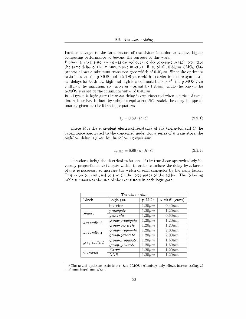
2.2 Transistor sizing
In a digital circuit transistors sizing should meet both area occupation and per-formance speci�cations. Since the purpose of this work is only to verify thebehavior of the examined structures, only preliminary sizing was carried out.
49
2.2. Transistor sizing
Further changes to the form factors of transistors in order to achieve highercomputing performance go beyond the purpose of this work.Preliminary transistor sizing was carried out in order to ensure to each logic gatethe same delay of the minimum size inverter. First of all, 0.35µm CMOS C35process allows a minimum transistor gate width of 0.40µm. Since the optimumratio between the p-MOS and n-MOS gate width in order to ensure symmetri-cal delays for both low-high and high-low commutations is 31, the p-MOS gatewidth of the minimum size inverter was set to 1.20µm, while the one of then-MOS was set to the minimum value of 0.40µm.In a Dynamic logic gate the worst delay is experimented when a series of tran-sistors is active. In fact, by using an equivalent RC model, the delay is approx-imately given by the following equation:
tp = 0.69 ·R · C (2.2.1)
where R is the equivalent electrical resistance of the transistor and C thecapacitance associated to the concerned node. For a series of n transistors, thehigh-low delay is given by the following equation:
tp,HL = 0.69 · n ·R · C (2.2.2)
Therefore, being the electrical resistance of the transistor approximately in-versely proportional to its gate width, in order to reduce the delay by a factorof n it is necessary to increase the width of each transistor by the same factor.This criterion was used to size all the logic gates of the adder. The followingtable summarizes the size of the transistors in each logic gate.
Transistor sizeBlock Logic gate p-MOS n-MOS (each)
inverter 1.20µm 0.40µm
squarepropagate 1.20µm 1.20µmgenerate 1.20µm 0.60µm
dot radix-2group-propagate 1.20µm 1.20µmgroup-generate 1.20µm 1.20µm
dot radix-4group-propagate 1.20µm 2.00µmgroup-generate 1.20µm 2.00µm
grey radix-4group-propagate 1.20µm 1.60µmgroup-generate 1.20µm 1.60µm
diamondCarry 1.20µm 1.20µmXOR 1.20µm 1.20µm
1The actual optimum ratio is 2.4, but CMOS technology only allows integer scaling ofminimum length and width.
50
2.3. Simulation
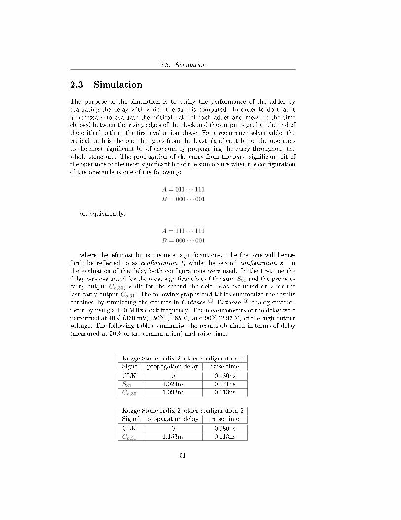
2.3 Simulation
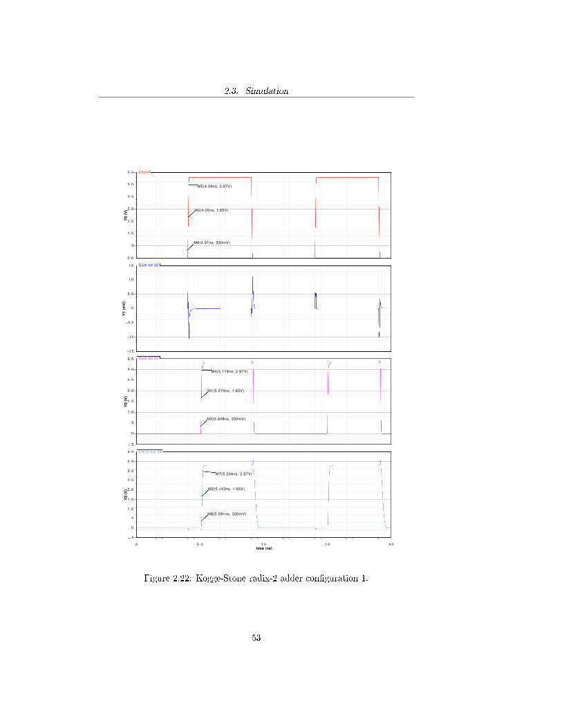
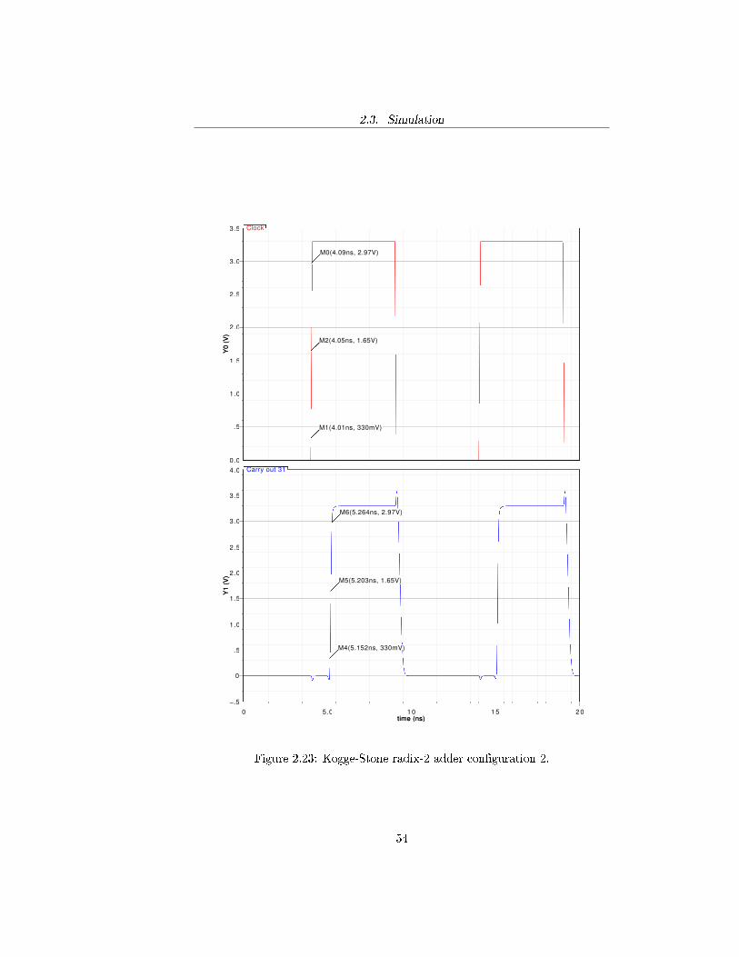
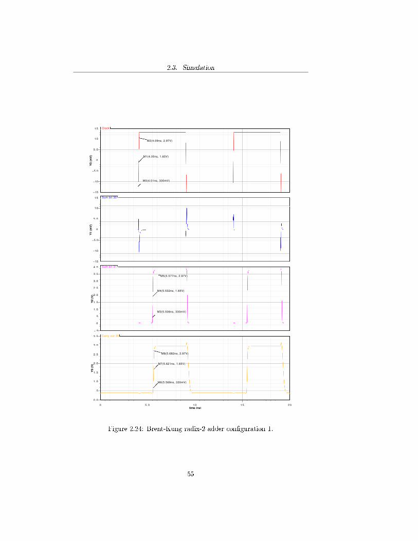
The purpose of the simulation is to verify the performance of the adder byevaluating the delay with which the sum is computed. In order to do that itis necessary to evaluate the critical path of each adder and measure the timeelapsed between the rising edges of the clock and the output signal at the end ofthe critical path at the �rst evaluation phase. For a recurrence solver adder thecritical path is the one that goes from the least signi�cant bit of the operandsto the most signi�cant bit of the sum by propagating the carry throughout thewhole structure. The propagation of the carry from the least signi�cant bit ofthe operands to the most signi�cant bit of the sum occurs when the con�gurationof the operands is one of the following:
A = 011 · · · 111B = 000 · · · 001
or, equivalently:
A = 111 · · · 111B = 000 · · · 001
where the leftmost bit is the most signi�cant one. The �rst one will hence-forth be re�erred to as con�guration 1, while the second con�guration 2. Inthe evaluation of the delay both con�gurations were used. In the �rst one thedelay was evaluated for the most signi�cant bit of the sum S31 and the previouscarry output Co,30, while for the second the delay was evaluated only for thelast carry output Co,31. The following graphs and tables summarize the resultsobtained by simulating the circuits in Cadence R© Virtuoso R© analog environ-ment by using a 100 MHz clock frequency. The measurements of the delay wereperformed at 10% (330 mV), 50% (1.65 V) and 90% (2.97 V) of the high outputvoltage. The following tables summarize the results obtained in terms of delay(measured at 50% of the commutation) and raise time.
Kogge-Stone radix-2 adder con�guration 1Signal propagation delay raise time
CLK 0 0.080nsS31 1.024ns 0.071nsCo,30 1.093ns 0.113ns
Kogge-Stone radix-2 adder con�guration 2Signal propagation delay raise time
CLK 0 0.080nsCo,31 1.153ns 0.113ns
51
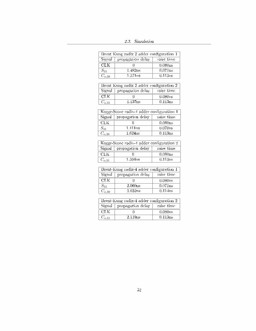
2.3. Simulation
Brent-Kung radix-2 adder con�guration 1Signal propagation delay raise time
CLK 0 0.080nsS31 1.482ns 0.071nsCo,30 1.571ns 0.113ns
Brent-Kung radix-2 adder con�guration 2Signal propagation delay raise time
CLK 0 0.080nsCo,31 1.137ns 0.113ns
Kogge-Stone radix-4 adder con�guration 1Signal propagation delay raise time
CLK 0 0.080nsS31 1.411ns 0.070nsCo,30 1.624ns 0.113ns
Kogge-Stone radix-4 adder con�guration 2Signal propagation delay raise time
CLK 0 0.080nsCo,31 1.594ns 0.113ns
Brent-Kung radix-4 adder con�guration 1Signal propagation delay raise time
CLK 0 0.080nsS31 2.060ns 0.071nsCo,30 2.032ns 0.114ns
Brent-Kung radix-4 adder con�guration 2Signal propagation delay raise time
CLK 0 0.080nsCo,31 2.119ns 0.113ns
52
2.3. Simulation
0 5.0 1 0 1 5 2 0time (ns)
3.5
3.0
2.5
2.0
1.5
1.0
.5
0.0
Y0
(V)
Y0
(V)
1 5
1 0
5.0
0
−5.0
−10
−15
Y1
(mV
)Y
1(m
V)
3 .5
3.0
2.5
2.0
1.5
1.0
.5
0
−.5
Y2
(V)
Y2
(V)
4 .0
3.5
3.0
2.5
2.0
1.5
1.0
.5
0
−.5
Y3
(V)
Y3
(V)
Clock
Sum bit 30
Sum bit 31
Carry out 30
M3(5.048ns, 330mV)M3(5.048ns, 330mV)M3(5.048ns, 330mV)M3(5.048ns, 330mV)M3(5.048ns, 330mV)
M1(5.074ns, 1.65V)M1(5.074ns, 1.65V)M1(5.074ns, 1.65V)M1(5.074ns, 1.65V)M1(5.074ns, 1.65V)
M4(5.119ns, 2.97V)M4(5.119ns, 2.97V)M4(5.119ns, 2.97V)M4(5.119ns, 2.97V)M4(5.119ns, 2.97V)
M5(4.09ns, 2.97V)M5(4.09ns, 2.97V)M5(4.09ns, 2.97V)M5(4.09ns, 2.97V)M5(4.09ns, 2.97V)
M0(4.05ns, 1.65V)M0(4.05ns, 1.65V)M0(4.05ns, 1.65V)M0(4.05ns, 1.65V)M0(4.05ns, 1.65V)
M6(4.01ns, 330mV)M6(4.01ns, 330mV)M6(4.01ns, 330mV)M6(4.01ns, 330mV)M6(4.01ns, 330mV)
M7(5.204ns, 2.97V)M7(5.204ns, 2.97V)M7(5.204ns, 2.97V)M7(5.204ns, 2.97V)M7(5.204ns, 2.97V)
M8(5.091ns, 330mV)M8(5.091ns, 330mV)M8(5.091ns, 330mV)M8(5.091ns, 330mV)M8(5.091ns, 330mV)
M2(5.143ns, 1.65V)M2(5.143ns, 1.65V)M2(5.143ns, 1.65V)M2(5.143ns, 1.65V)M2(5.143ns, 1.65V)
time (ns)
Figure 2.22: Kogge-Stone radix-2 adder con�guration 1.
53
2.3. Simulation
0 5.0 10 15 20time (ns)
3.5
3.0
2.5
2.0
1.5
1.0
.5
0.0
Y0(V)
Y0(V)
4 .0
3.5
3.0
2.5
2.0
1.5
1.0
.5
0
−.5
Y1(V)
Y1(V)
Clock
Carry out 31
M1(4.01ns, 330mV)M1(4.01ns, 330mV)M1(4.01ns, 330mV)M1(4.01ns, 330mV)M1(4.01ns, 330mV)
M0(4.09ns, 2.97V)M0(4.09ns, 2.97V)M0(4.09ns, 2.97V)M0(4.09ns, 2.97V)M0(4.09ns, 2.97V)
M2(4.05ns, 1.65V)M2(4.05ns, 1.65V)M2(4.05ns, 1.65V)M2(4.05ns, 1.65V)M2(4.05ns, 1.65V)
M4(5.152ns, 330mV)M4(5.152ns, 330mV)M4(5.152ns, 330mV)M4(5.152ns, 330mV)M4(5.152ns, 330mV)
M5(5.203ns, 1.65V)M5(5.203ns, 1.65V)M5(5.203ns, 1.65V)M5(5.203ns, 1.65V)M5(5.203ns, 1.65V)
M6(5.264ns, 2.97V)M6(5.264ns, 2.97V)M6(5.264ns, 2.97V)M6(5.264ns, 2.97V)M6(5.264ns, 2.97V)
time (ns)
Figure 2.23: Kogge-Stone radix-2 adder con�guration 2.
54
2.3. Simulation
0 5.0 1 0 1 5 2 0time (ns)
1 5
1 0
5.0
0
−5.0
−10
−15
Y0(m
V)
Y0(m
V)
3 .5
3.0
2.5
2.0
1.5
1.0
.5
0
−.5
Y1(V)
Y1(V)
4 .0
3.5
3.0
2.5
2.0
1.5
1.0
.5
0
−.5
Y2(V)
Y2(V)
3 .5
3.0
2.5
2.0
1.5
1.0
.5
0.0
Y3(V)
Y3(V)
Clock
Sum bit 30
Sum bit 31
Carry out 30
M0(4.01ns, 330mV)M0(4.01ns, 330mV)M0(4.01ns, 330mV)M0(4.01ns, 330mV)M0(4.01ns, 330mV)
M1(4.05ns, 1.65V)M1(4.05ns, 1.65V)M1(4.05ns, 1.65V)M1(4.05ns, 1.65V)M1(4.05ns, 1.65V)
M2(4.09ns, 2.97V)M2(4.09ns, 2.97V)M2(4.09ns, 2.97V)M2(4.09ns, 2.97V)M2(4.09ns, 2.97V)
M3(5.506ns, 330mV)M3(5.506ns, 330mV)M3(5.506ns, 330mV)M3(5.506ns, 330mV)M3(5.506ns, 330mV)
M4(5.532ns, 1.65V)M4(5.532ns, 1.65V)M4(5.532ns, 1.65V)M4(5.532ns, 1.65V)M4(5.532ns, 1.65V)
M5(5.577ns, 2.97V)M5(5.577ns, 2.97V)M5(5.577ns, 2.97V)M5(5.577ns, 2.97V)M5(5.577ns, 2.97V)
M6(5.569ns, 330mV)M6(5.569ns, 330mV)M6(5.569ns, 330mV)M6(5.569ns, 330mV)M6(5.569ns, 330mV)
M7(5.621ns, 1.65V)M7(5.621ns, 1.65V)M7(5.621ns, 1.65V)M7(5.621ns, 1.65V)M7(5.621ns, 1.65V)
M8(5.682ns, 2.97V)M8(5.682ns, 2.97V)M8(5.682ns, 2.97V)M8(5.682ns, 2.97V)M8(5.682ns, 2.97V)
time (ns)0 5.0 1 0 1 5 2 0
time (ns)
3.5
3.0
2.5
2.0
1.5
1.0
.5
0.0
Y0(V)
Y0(V)
1 5
1 0
5.0
0
−5.0
−10
−15
Y1(m
V)
Y1(m
V)
3 .5
3.0
2.5
2.0
1.5
1.0
.5
0
−.5
Y2(V)
Y2(V)
4 .0
3.5
3.0
2.5
2.0
1.5
1.0
.5
0
−.5
Y3(V)
Y3(V)
Clock
Sum bit 30
Sum bit 31
Carry out 30
M3(5.048ns, 330mV)M3(5.048ns, 330mV)M3(5.048ns, 330mV)M3(5.048ns, 330mV)M3(5.048ns, 330mV)
M1(5.074ns, 1.65V)M1(5.074ns, 1.65V)M1(5.074ns, 1.65V)M1(5.074ns, 1.65V)M1(5.074ns, 1.65V)
M4(5.119ns, 2.97V)M4(5.119ns, 2.97V)M4(5.119ns, 2.97V)M4(5.119ns, 2.97V)M4(5.119ns, 2.97V)
M5(4.09ns, 2.97V)M5(4.09ns, 2.97V)M5(4.09ns, 2.97V)M5(4.09ns, 2.97V)M5(4.09ns, 2.97V)
M0(4.05ns, 1.65V)M0(4.05ns, 1.65V)M0(4.05ns, 1.65V)M0(4.05ns, 1.65V)M0(4.05ns, 1.65V)
M6(4.01ns, 330mV)M6(4.01ns, 330mV)M6(4.01ns, 330mV)M6(4.01ns, 330mV)M6(4.01ns, 330mV)
M7(5.204ns, 2.97V)M7(5.204ns, 2.97V)M7(5.204ns, 2.97V)M7(5.204ns, 2.97V)M7(5.204ns, 2.97V)
M8(5.091ns, 330mV)M8(5.091ns, 330mV)M8(5.091ns, 330mV)M8(5.091ns, 330mV)M8(5.091ns, 330mV)
M2(5.143ns, 1.65V)M2(5.143ns, 1.65V)M2(5.143ns, 1.65V)M2(5.143ns, 1.65V)M2(5.143ns, 1.65V)
time (ns)
Figure 2.24: Brent-Kung radix-2 adder con�guration 1.
55
2.3. Simulation
0 5.0 10 15 20time (ns)
3.5
3.0
2.5
2.0
1.5
1.0
.5
0.0
Y0(V)
Y0(V)
4 .0
3.5
3.0
2.5
2.0
1.5
1.0
.5
0
−.5
Y1(V)
Y1(V)
Clock
Carry out 31
M0(4.01ns, 330mV)M0(4.01ns, 330mV)M0(4.01ns, 330mV)M0(4.01ns, 330mV)M0(4.01ns, 330mV)
M1(4.05ns, 1.65V)M1(4.05ns, 1.65V)M1(4.05ns, 1.65V)M1(4.05ns, 1.65V)M1(4.05ns, 1.65V)
M2(4.09ns, 2.97V)M2(4.09ns, 2.97V)M2(4.09ns, 2.97V)M2(4.09ns, 2.97V)M2(4.09ns, 2.97V)
M3(5.136ns, 330mV)M3(5.136ns, 330mV)M3(5.136ns, 330mV)M3(5.136ns, 330mV)M3(5.136ns, 330mV)
M4(5.187ns, 1.65V)M4(5.187ns, 1.65V)M4(5.187ns, 1.65V)M4(5.187ns, 1.65V)M4(5.187ns, 1.65V)
M5(5.249ns, 2.97V)M5(5.249ns, 2.97V)M5(5.249ns, 2.97V)M5(5.249ns, 2.97V)M5(5.249ns, 2.97V)
time (ns)
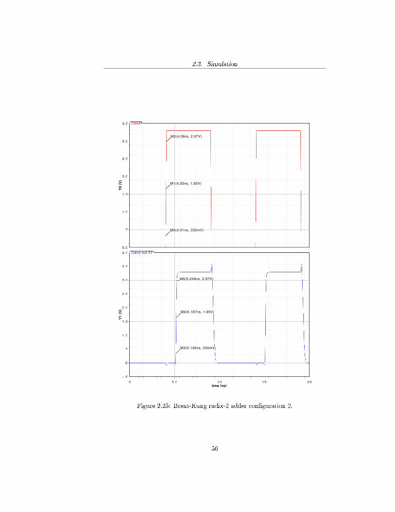
Figure 2.25: Brent-Kung radix-2 adder con�guration 2.
56
2.3. Simulation
0 5.0 1 0 1 5 2 0time (ns)
3.5
3.0
2.5
2.0
1.5
1.0
.5
0.0
Y0(V)
Y0(V)
1 5
1 0
5.0
0
−5.0
−10
−15
Y1(m
V)
Y1(m
V)
3 .5
3.0
2.5
2.0
1.5
1.0
.5
0
−.5
Y2(V)
Y2(V)
4 .0
3.5
3.0
2.5
2.0
1.5
1.0
.5
0
−.5
Y3(V)
Y3(V)
Clock
Sum bit 30
Sum bit 31
Carry out 30
M0(4.01ns, 330mV)M0(4.01ns, 330mV)M0(4.01ns, 330mV)M0(4.01ns, 330mV)M0(4.01ns, 330mV)
M1(4.05ns, 1.65V)M1(4.05ns, 1.65V)M1(4.05ns, 1.65V)M1(4.05ns, 1.65V)M1(4.05ns, 1.65V)
M2(4.09ns, 2.97V)M2(4.09ns, 2.97V)M2(4.09ns, 2.97V)M2(4.09ns, 2.97V)M2(4.09ns, 2.97V)
M3(5.436ns, 330mV)M3(5.436ns, 330mV)M3(5.436ns, 330mV)M3(5.436ns, 330mV)M3(5.436ns, 330mV)
M4(5.461ns, 1.65V)M4(5.461ns, 1.65V)M4(5.461ns, 1.65V)M4(5.461ns, 1.65V)M4(5.461ns, 1.65V)
M5(5.506ns, 2.97V)M5(5.506ns, 2.97V)M5(5.506ns, 2.97V)M5(5.506ns, 2.97V)M5(5.506ns, 2.97V)
M6(5.561ns, 330mV)M6(5.561ns, 330mV)M6(5.561ns, 330mV)M6(5.561ns, 330mV)M6(5.561ns, 330mV)
M7(5.613ns, 1.65V)M7(5.613ns, 1.65V)M7(5.613ns, 1.65V)M7(5.613ns, 1.65V)M7(5.613ns, 1.65V)
M8(5.674ns, 2.97V)M8(5.674ns, 2.97V)M8(5.674ns, 2.97V)M8(5.674ns, 2.97V)M8(5.674ns, 2.97V)
time (ns)
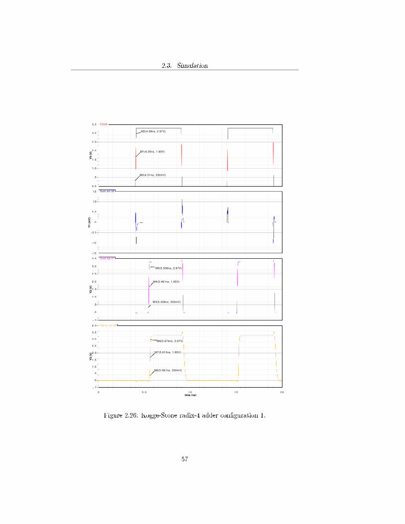
Figure 2.26: Kogge-Stone radix-4 adder con�guration 1.
57
2.3. Simulation
0 5.0 10 15 20time (ns)
3.5
3.0
2.5
2.0
1.5
1.0
.5
0.0
Y0(V)
Y0(V)
4 .0
3.5
3.0
2.5
2.0
1.5
1.0
.5
0
−.5
Y1(V)
Y1(V)
Clock
Carry out 31
M0(4.01ns, 330mV)M0(4.01ns, 330mV)M0(4.01ns, 330mV)M0(4.01ns, 330mV)M0(4.01ns, 330mV)
M1(4.05ns, 1.65V)M1(4.05ns, 1.65V)M1(4.05ns, 1.65V)M1(4.05ns, 1.65V)M1(4.05ns, 1.65V)
M2(4.09ns, 2.97V)M2(4.09ns, 2.97V)M2(4.09ns, 2.97V)M2(4.09ns, 2.97V)M2(4.09ns, 2.97V)
M3(5.592ns, 330mV)M3(5.592ns, 330mV)M3(5.592ns, 330mV)M3(5.592ns, 330mV)M3(5.592ns, 330mV)
M4(5.644ns, 1.65V)M4(5.644ns, 1.65V)M4(5.644ns, 1.65V)M4(5.644ns, 1.65V)M4(5.644ns, 1.65V)
M5(5.705ns, 2.97V)M5(5.705ns, 2.97V)M5(5.705ns, 2.97V)M5(5.705ns, 2.97V)M5(5.705ns, 2.97V)
time (ns)
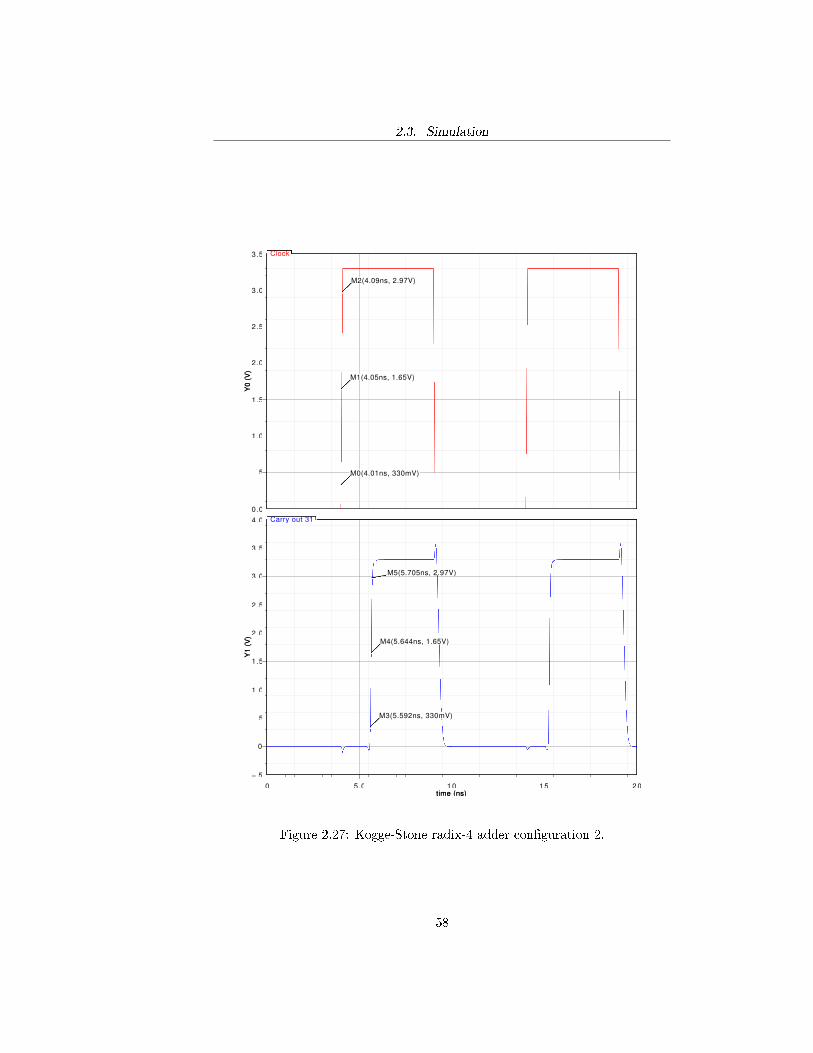
Figure 2.27: Kogge-Stone radix-4 adder con�guration 2.
58
2.3. Simulation
0 5.0 1 0 1 5 2 0time (ns)
3.5
3.0
2.5
2.0
1.5
1.0
.5
0.0
Y0(V)
Y0(V)
1 5
1 0
5.0
0
−5.0
−10
−15
Y1(m
V)
Y1(m
V)
3 .5
3.0
2.5
2.0
1.5
1.0
.5
0
−.5
Y2(V)
Y2(V)
4 .0
3.5
3.0
2.5
2.0
1.5
1.0
.5
0
−.5
Y3(V)
Y3(V)
Clock
Sum bit 30
Sum bit 31
Carry out 30
M0(4.01ns, 330mV)M0(4.01ns, 330mV)M0(4.01ns, 330mV)M0(4.01ns, 330mV)M0(4.01ns, 330mV)
M1(4.05ns, 1.65V)M1(4.05ns, 1.65V)M1(4.05ns, 1.65V)M1(4.05ns, 1.65V)M1(4.05ns, 1.65V)
M2(4.09ns, 2.97V)M2(4.09ns, 2.97V)M2(4.09ns, 2.97V)M2(4.09ns, 2.97V)M2(4.09ns, 2.97V)
M3(6.03ns, 330mV)M3(6.03ns, 330mV)M3(6.03ns, 330mV)M3(6.03ns, 330mV)M3(6.03ns, 330mV)
M4(6.056ns, 1.65V)M4(6.056ns, 1.65V)M4(6.056ns, 1.65V)M4(6.056ns, 1.65V)M4(6.056ns, 1.65V)
M5(6.101ns, 2.97V)M5(6.101ns, 2.97V)M5(6.101ns, 2.97V)M5(6.101ns, 2.97V)M5(6.101ns, 2.97V)
M6(6.03ns, 330mV)M6(6.03ns, 330mV)M6(6.03ns, 330mV)M6(6.03ns, 330mV)M6(6.03ns, 330mV)
M7(6.082ns, 1.65V)M7(6.082ns, 1.65V)M7(6.082ns, 1.65V)M7(6.082ns, 1.65V)M7(6.082ns, 1.65V)
M8(6.144ns, 2.97V)M8(6.144ns, 2.97V)M8(6.144ns, 2.97V)M8(6.144ns, 2.97V)M8(6.144ns, 2.97V)
time (ns)
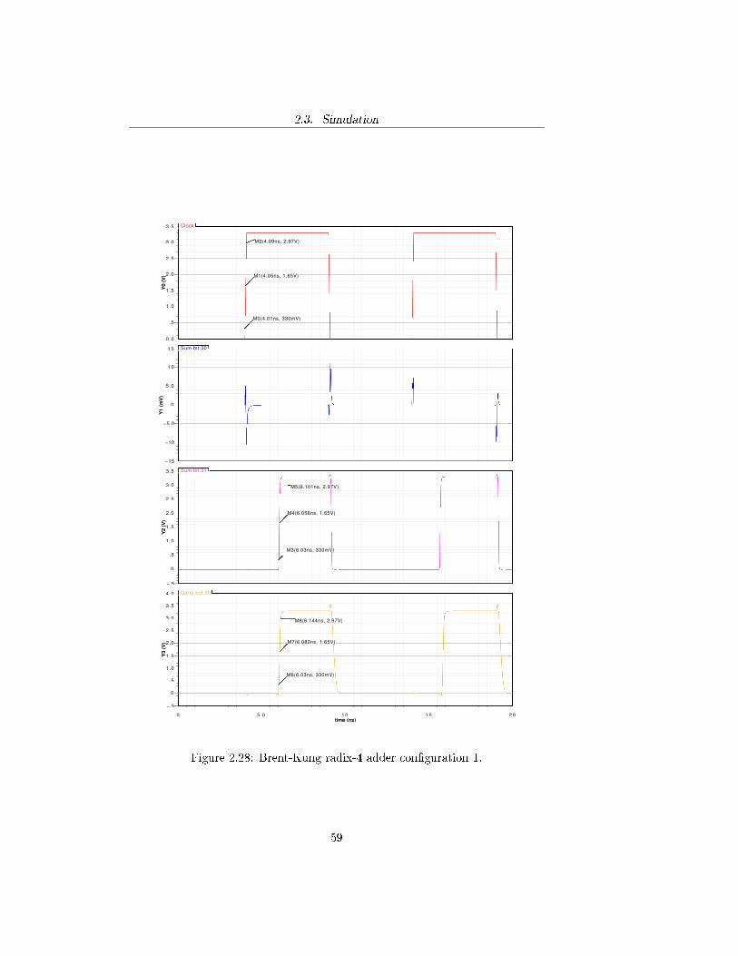
Figure 2.28: Brent-Kung radix-4 adder con�guration 1.
59
2.3. Simulation
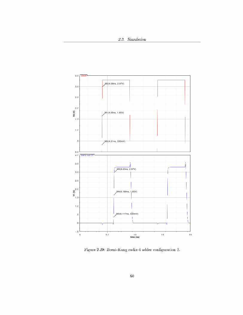
0 5.0 10 15 20time (ns)
3.5
3.0
2.5
2.0
1.5
1.0
.5
0.0
Y0(V)
Y0(V)
4 .0
3.5
3.0
2.5
2.0
1.5
1.0
.5
0
−.5
Y1(V)
Y1(V)
Clock
Carry out 31
M0(4.01ns, 330mV)M0(4.01ns, 330mV)M0(4.01ns, 330mV)M0(4.01ns, 330mV)M0(4.01ns, 330mV)
M1(4.05ns, 1.65V)M1(4.05ns, 1.65V)M1(4.05ns, 1.65V)M1(4.05ns, 1.65V)M1(4.05ns, 1.65V)
M2(4.09ns, 2.97V)M2(4.09ns, 2.97V)M2(4.09ns, 2.97V)M2(4.09ns, 2.97V)M2(4.09ns, 2.97V)
M3(6.117ns, 330mV)M3(6.117ns, 330mV)M3(6.117ns, 330mV)M3(6.117ns, 330mV)M3(6.117ns, 330mV)
M4(6.169ns, 1.65V)M4(6.169ns, 1.65V)M4(6.169ns, 1.65V)M4(6.169ns, 1.65V)M4(6.169ns, 1.65V)
M5(6.23ns, 2.97V)M5(6.23ns, 2.97V)M5(6.23ns, 2.97V)M5(6.23ns, 2.97V)M5(6.23ns, 2.97V)
time (ns)
Figure 2.29: Brent-Kung radix-4 adder con�guration 2.
60
2.3. Simulation
Simulations show that the recurrence solver adders tested introduce a delaywhich has an order of magnitude of nanonseconds. As predicted, in both radix-2and radix-4 cases Kogge-Stone adder topology has the highest computationalspeed compared to Brent-Kung architecture. On the other hand, area occu-pation of Kogge-Stone adder is much greater than the one used to implementBrent-Kung adder: 2669 to 1733 transistors for the radix-2 case and 1896 to1618 for the radix-4 case. Consequently, the power consumption of the Kogge-Stone topology is much greater than the one of Brent-Kung topology.
61

Conclusion
As a conclusion to the work, the importance of both theory and simulationin the design of a complex logic circuit must be underlined. On the one hand,theoretical research lays the fundation to the creation of increasingly performantstructures by perfectioning the logical and topological aspects of the circuit. Onthe other hand, simulation and veri�cation of the theoretical results representsan essential part of the design of all digital and analog circuits. In fact, manualcalculations alone are insu�cient in order to implement a circuit and can only beregarded as a �rst step towards the realization of the system. Moreover, furtheroptimization of the circuit can be achieved only by ulterior calculations andsimulations through which the designer can discern various structures in order tomeet speci�cations in terms of computational performance, power consumptionand area occupation.
63
2.3. Simulation
64
Bibliography
[1] Jan M. Rabaey, Anantha Chandrakasan, Borivoje Nikoli¢, Digital IntegratedCircuits, A Design Perspective, Prentice Hall, 2nd edition, 2003. ISBN: 0-13-120764-4.
[2] R. Brent and H.T. Kung, �A regular Layout for Parallel Adders", IEEETrans. on Computers, vol. C-31, no. 3, pp. 260-264, March 1982.
[3] P.M. Kogge and H.S. Stone, �A Parallel Algorithm for the E�cient Solutionof a General Class of Recurrence Equations", IEEE Trans. on Computers,vol. C-22, pp. 786-793, August 1973.
[4] Hoang Q. Dao and Vojin Oklobdzija, �Performance Comparison of VLSIAdders Using Logical E�ort", PATMOS 2002, LNCS 2451, pp. 25-34, 2002,Springer-Verlag Berlin Heidelberg.
[5] Vojin Oklobdzija, �High-Speed VLSI Arithmetic Units: Adders and Multipli-ers in Design of High-Performance Microprocessor Circuits", Book Chapter4, Book edited by A. Chandrakasan, IEEE Press, 2000.
[6] J. A. Abraham, �Design of Adders", Lecture slides, EE-382M.7, Departmentof Electrical and Computer Engineering, The University of Texas at Austin,September 21, 2011.
65