Embed Size (px)
Citation preview
Study and characterization of the ZnPc:C60/MoOx
interface in organic solar cells by means of photoelectron
spectroscopy
Caterina Stenta
April, 2013
Dissertation to obtain the academic degree of
Master in materials engineering
submitted to the
Faculty of science and engineering of Universidade Nova de Lisboa
prepared at the
Helmholtz-Zentrum Berlin für Materialien und Energie

Supervisor: Prof. Dr. João Pedro Veiga
Co-supervisor: Dr. Iver Lauermann
ii

Study and characterization of the ZnPc:C60/MoOx interface in organic solar
cells by means of photoelectron spectroscopy
Copyright © em nome de: Caterina Stenta; Faculdade de Ciências e Tecnologia, Uni-
versidade Nova de Lisboa
A Faculdade de Ciências e Tecnologia e a Universidade Nova de Lisboa tem o direito,
perpétuo e sem limites geográ�cos, de arquivar e publicar esta dissertação através de
exemplares impressos reproduzidos em papel ou de forma digital, ou por qualquer outro
meio conhecido ou que venha a ser inventado, e de a divulgar atraves de repositórios
cientí�cos e de admitir a sua cópia e distribuição com objectivos educacionais ou de
investigação, não comerciais, desde que seja dado crédito ao autor e editor.
iii

For my family
�Life is and will ever remain an equation incapable
of solution, but it contains certain known factors.�
Nikola Tesla
iv

Contents
Acknowledgments vii
List of symbols and abbreviations viii
List of �gures xi
List of tables xiii
Resumo xiv
Abstract xv
1 Introduction 11.1 Device structure and operating principles . . . . . . . . . . . . . . . 2
1.2 Photovoltaic performance characteristics . . . . . . . . . . . . . . . . 4
1.2.1 Electrical model . . . . . . . . . . . . . . . . . . . . . . . . . . 4
1.2.2 Power conversion e�ciency . . . . . . . . . . . . . . . . . . . 7
1.2.3 Fill factor . . . . . . . . . . . . . . . . . . . . . . . . . . . . . . 7
1.2.4 Open circuit voltage . . . . . . . . . . . . . . . . . . . . . . . 8
1.2.5 Short circuit current density . . . . . . . . . . . . . . . . . . 9
2 Materials 112.1 Substrate and front electrode . . . . . . . . . . . . . . . . . . . . . . 11
2.2 The intermediate layer . . . . . . . . . . . . . . . . . . . . . . . . . . 12
2.3 The active layer . . . . . . . . . . . . . . . . . . . . . . . . . . . . . . . 13
2.3.1 Fullerene . . . . . . . . . . . . . . . . . . . . . . . . . . . . . . 13
2.3.2 Donor material . . . . . . . . . . . . . . . . . . . . . . . . . . . 13
2.4 The back electrode . . . . . . . . . . . . . . . . . . . . . . . . . . . . . 14
2.5 Final structure . . . . . . . . . . . . . . . . . . . . . . . . . . . . . . . 14
3 Surface characterization techniques 163.1 UPS . . . . . . . . . . . . . . . . . . . . . . . . . . . . . . . . . . . . . 16
3.2 XPS . . . . . . . . . . . . . . . . . . . . . . . . . . . . . . . . . . . . . 17
3.3 Synchrotron . . . . . . . . . . . . . . . . . . . . . . . . . . . . . . . . . 19
4 Experimental 234.1 Preparation of the samples . . . . . . . . . . . . . . . . . . . . . . . . 23
4.1.1 Organic layer deposition . . . . . . . . . . . . . . . . . . . . . 24
4.1.2 Bu�er layer deposition . . . . . . . . . . . . . . . . . . . . . . 25
4.1.3 Silver contacts deposition . . . . . . . . . . . . . . . . . . . . 26
4.2 Optical measurements . . . . . . . . . . . . . . . . . . . . . . . . . . . 26
4.3 Characterization at CISSY of the ZnPc:C60/MoOx interface . . . . 28
4.3.1 Ultraviolet photoelectron spectroscopy . . . . . . . . . . . . 29
4.3.2 X-ray photoelectron spectroscopy . . . . . . . . . . . . . . . 31
4.4 Temperature dependent J(V) measurements . . . . . . . . . . . . . 38
v

4.5 Temperature dependent photoelectron spectroscopy analysis . . . . 39
4.5.1 Peak�t . . . . . . . . . . . . . . . . . . . . . . . . . . . . . . . . 43
4.6 NEXAFS measurements . . . . . . . . . . . . . . . . . . . . . . . . . 43
5 Discussion and conclusions 465.1 Band alignment from UPS analysis . . . . . . . . . . . . . . . . . . . 46
5.2 PV parameters . . . . . . . . . . . . . . . . . . . . . . . . . . . . . . . 49
5.3 XPS annealing results . . . . . . . . . . . . . . . . . . . . . . . . . . . 53
5.4 Concluding remarks . . . . . . . . . . . . . . . . . . . . . . . . . . . . 54
vi

Acknowledgments
I would like to thank Prof. Dr. Martha Ch. Lux-Steiner for giving me the opportunity to workon my thesis in her department at Helmholtz Zentrum Berlin.
Special thanks go to Dr. Iver Lauermann for letting me realize this work in his group, for hisscienti�c supervision, guidance and for the proof-reading of this work.
I am very thankful to the CISSY group, Dr. Iver Lauermann, Alexander Steigert, Britta Höpfnerand Lisa Risch for the discussions in the interpretation of XPS and UPS results, for helping me duringmy experience at the Helmholtz Zentrum Berlin and for the overall support.
I am very thankful to Dr. Marin Rusu for the support and guidance during the IVT measurementsand for the fruitful discussions, and to Sven Wiesner, Volker Hinrichs and Tayfun Mete for helpingme with the interpretation of the IVT results and for the support during the experimental work inWannsee.
I would like to thank Prof. João Paulo Borges for the technical support and João Pedro Veigafor the guidance, the enthusiasm and the dissertation corrections.
vii

List of symbols and abbreviations
A Diode quality factor
AFM Atomic force microscope
AM1.5G Air Mass 1.5 Global
a.u. Arbitrary units
a Absorption coe�cient
BE Binding energy
EC Conduction band minimum
EF Fermi level
Eg Band gap energy
Ek Kinetic energy
EQE External quantum e�ciency
ESCA Electron spectroscopy for chemical analysis
EV Valence band maximum
NEXAFS Near edge X-ray absorption �ne structure
er Relative dielectric constant
FF Fill factor
f Work function
fs Spectrometer work function
h Energy conversion e�ciency
h Planck's constant
HOMO Highest occupied molecular orbit
I Current
viii

Iilu Illumination intensity
I0 Initial light intensity
Isc Short circuit current
ITO Indium tin oxide
J Current density
J0 Saturation current density
Jm Current density at maximum power point
Jsc Short circuit current density
LUMO Lowest unoccupied molecular orbit
k Boltzmann constant
KPFM Kelvin probe force microscope
m Charge mobility
n Excitonic di�usion length
h E�ciency
OVPD Organic vapour phase deposition
OPV Organic photovoltaic
OSC Organic solar cell
PCE Power conversion e�ciency
PES Photoelectron spectroscopy
Pin Power of the incident light
Pmax Maximum power
PV Photovoltaic
R2R Roll to roll machinery
ix

q Elementary electric charge
RlLoad Resistor
Rs Series resistance
RshShunt resistance
l Inelastic mean free path or wavelenght
n Frequency
R Re�ectance
SECO Secondary electron cuto�
SEM Scanning electron microscope
t Thickness
T Transmission or Temperature
UHV Ultra high vacuum
UPS Ultraviolet photoelectron spectroscopy
UV Ultraviolet
VB Valence band
Vis Visible
Voc Open circuit voltage
Vm Voltage at maximum power point
VPD Vapour phase deposition
VTE Vacuum thermal evaporation
Wf Workfunction
XES X-ray emission spectroscopy
XPS X-ray photoelectron spectroscopy
Square
x

List of �gures
1.1 General energy band diagram of the heterojunction in a hybrid solar cell. . . . . . . . . . . . . 3
1.2 Schematic diagram presenting the charge transfer for a photo generation in the electron
donor material. . . . . . . . . . . . . . . . . . . . . . . . . . . . . . . . . . . . . . . . . . . . . . . . . . . . . . . . . . . . . . . . . . . . . . . 3
1.3 a) Equivalent electrical circuit and b) characteristic of the dark and illuminated solar
cell. . . . . . . . . . . . . . . . . . . . . . . . . . . . . . . . . . . . . . . . . . . . . . . . . . . . . . . . . . . . . . . . . . . . . . . . . . . . . . . . . . 6
1.4 Current-voltage characteristic for a generic illuminated solar
n cell. . . . . . . . . . . . . . . . . . . . . . . . . . . . . . . . . . . . . . . . . . . . . . . . . . . . . . . . . . . . . . . . . . . . . . . . . . . . . . . . . . 7
1.5 Energy band diagram illustrating the �ve steps in the charge transfer process. The
e�ciency of these steps determines the EQE of the hybrid device. . . . . . . . . . . . . . . . . . . 10
2.1 Schematic bulk heterojunction structure for the inverted solar cell used in this work. 11
2.2 Chemical structure of (a) zinc phthalocyanine and (b) fullerene C60.
n . . . . . . . . . . . . . . . . . . . . . . . . . . . . . . . . . . . . . . . . . . . . . . . . . . . . . . . . . . . . . . . . . . . . . . . . . . . . . . . . . . . . 14
2.3 Schematic overview structure of the solar cell with ZnPc and C60 as photoactive layer.
The investigated interface is shown. . . . . . . . . . . . . . . . . . . . . . . . . . . . . . . . . . . . . . . . . . . . . . . . . . 15
3.1 Diagram of the photoelectric process (top) and the Auger process (bottom). . . . . . . . . 18
3.2 The mean free paths of the electrons in solid. . . . . . . . . . . . . . . . . . . . . . . . . . . . . . . . . . . . . . . . 19
4.1 Scanning electron micrographs of the cross-section of physically deposited MoOx on
ZnO:Al. Shown in the upper micrograph are the data used for evaluation of the thickness
24
4.2 Schematic drawing of the OPVD apparatus. . . . . . . . . . . . . . . . . . . . . . . . . . . . . . . . . . . . . . . . . 26
4.3 (ahv)2 vs. photon energy for ZnO:Al/quartz and 100 nm
m MoOx/quartz. . . . . . . . . . . . . . . . . . . . . . . . . . . . . . . . . . . . . . . . . . . . . . . . . . . . . . . . . . . . . . . . . . . . . . . 27
4.4 Schematic diagram of the CISSY experimental end station. . . . . . . . . . . . . . . . . . . . . . . . . . 28
xi

4.5 Photo of the CISSY experimental station were photoelectron spectroscopy measurements
have been carried out. . . . . . . . . . . . . . . . . . . . . . . . . . . . . . . . . . . . . . . . . . . . . . . . . . . . . . . . . . . . . . . 29
4.6 Ultraviolet photoelectron spectra for 0, 0.5 and 1 nm MoOx showing the valence band
maximum. The zero in the abscissa corresponds to the Fermi level which is obtained by
measuring the Fermi edge of a gold foil with UPS. The spectra are recorded using the
UV radiation source of He I (hn=21.22 eV). . . . . . . . . . . . . . . . . . . . . . . . . . . . . . . . . . . . . . . . . . 31
4.7 XPS survey spectra of the ZnPc:C60 and MoOx interface for di�erent MoOx thicknesses.
33
4.8 XPS spectra of the Zn2p signal for di�erent MoOx thicknesses. The energetic positions
of the peaks are shown. . . . . . . . . . . . . . . . . . . . . . . . . . . . . . . . . . . . . . . . . . . . . . . . . . . . . . . . . . . . . . 34
4.9 Zn2p peak position shift as function of the MoOx thickness. . . . . . . . . . . . . . . . . . . . . . . . . . 35
4.10 ZnLMM Auger peaks spectra.. . . . . . . . . . . . . . . . . . . . . . . . . . . . . . . . . . . . . . . . . . . . . . . . . . . . . . . .35
4.11 XPS MoOx spectra of 0.5 to 10 nm of MoOx bu�er layer samples together with the
reference sample of 100 nm MoOx. . . . . . . . . . . . . . . . . . . . . . . . . . . . . . . . . . . . . . . . . . . . . . . . . . . 36
4.12 XPS detailed spectra of C1s, O1s and N1s peaks signals. . . . . . . . . . . . . . . . . . . . . . . . . . . . 37
4.13 Graph of the annealing procedure. . . . . . . . . . . . . . . . . . . . . . . . . . . . . . . . . . . . . . . . . . . . . . . . . . . 40
4.14 UPS spectra recorded during the annealing and after the cooling down for the sample
ZnO:Al/ 80 nm ZnPc:C60/ 5 nm MoOx. Temperature values from room temperature to
200 °C are shown. . . . . . . . . . . . . . . . . . . . . . . . . . . . . . . . . . . . . . . . . . . . . . . . . . . . . . . . . . . . . . . . . . . 41
4.15 UPS spectra in the region of the secondary emission curve for di�erent temperatures of
the annealing process for the sample ZnO:Al/ 80 nm ZnPc:C60/ 5 nm MoOx. Shown are
also the spectra recorded during the thermal process. . . . . . . . . . . . . . . . . . . . . . . . . . . . . . . . 41
4.16 XPS detailed spectra of the C1s, O1s, Na1s and Zn2p photoemission peaks for a 5
nm MoO3 sample at room temperature before the annealing procedure (blue), after the
annealing procedure (light blue), annealed at 160°C (orange) and 200°C (red). . . . . . . 42
4.17 NEXAFS spectra of the Zn2p in the range 1015 eV-1040 eV for 1 nm MoOx/80 nm
ZnPc:C60/ZnO:Al/Glass and 80 nm ZnPc:C60/ZnO:Al/ Glass samples.. . . . . . . . . . . . . .44
xii

5.1 Work function values in function of the MoOx thickness for two positions on the sample.
The margin error of 0.05 eV is
n indicated.. . . . . . . . . . . . . . . . . . . . . . . . . . . . . . . . . . . . . . . . . . . . . . . . . . . . . . . . . . . . . . . . . . . . . . . . . . .46
5.2 Schematic energy level diagram of the ZnPc:C60/MoO3 interface heterojunction. The
experimentally determined band gap values of bulk MoOx and the di�erence between
valence band levels and Fermi levels as well as the literature data are given. . . . . . . . . . 49
5.3 PV parameters as a function of temperature under AM 1.5 conditions (100mW/cm2).51
5.4 J-V curves of the annealed samples . . . . . . . . . . . . . . . . . . . . . . . . . . . . . . . . . . . . . . . . . . . . . . . . . 52
5.5 LogJ-V curves of the annealed samples. . . . . . . . . . . . . . . . . . . . . . . . . . . . . . . . . . . . . . . . . . . . . .52
5.6 Wf values for the sample in function of the annealing temperature for the sample ZnO:Al/
80 nm ZnPc:C60/ 5 nm MoOx. . . . . . . . . . . . . . . . . . . . . . . . . . . . . . . . . . . . . . . . . . . . . . . . . . . . . . .53
List of tables
4.1 Peaks positions of some spectral line of Zn, Mo, C, O and N.. . . . . . . . . . . . . . . . . . . . . . . .33
4.2 ZnLMM Auger peaks positions. . . . . . . . . . . . . . . . . . . . . . . . . . . . . . . . . . . . . . . . . . . . . . . . . . . . . . . 36
4.3 Peaks area of the main photoemission peaks at room temperature and after thermal
treatment of 200°C with their respective energetic positions. . . . . . . . . . . . . . . . . . . . . . . . . 43
5.1 Work function values obtained with KPFM and UPS analyses. . . . . . . . . . . . . . . . . . . . . . . 47
xiii

Resumo
A procura de sistemas fotovoltaicos de baixo custo tem levado à escolha de materiais orgânicos como
possíveis candidatos para substituir os dispositivos baseados em silício. Os materiais orgânicos têm
coe�cientes de absorção elevados, permitindo o uso de películas muito �nas e de técnicas de fabri-
cação de baixo custo. O controlo sobre a estrutura electrónica das interfaces orgânicas/inorgânicas
em semicondutores é um passo essencial para o desenvolvimento desses dispositivos. No presente
estudo esta questão é abordada numa célula solar orgânica com uma estrutura invertida, constituída
por uma camada fotoactiva orgânica de zinco ftalocianina dopada com Fulereno, um eléctrodo de
óxido de zinco dopado com alumínio, uma camada intermédia de óxido de molibdénio e por um
eléctrodo de prata. O objectivo deste trabalho foi o estudo e a caracterização das propriedades elec-
trónicas da interface MoOx / ZnPc: C60. Para este propósito recorreu-se à análise por espectroscopia
fotoeléctronica ultravioleta (UPS) para a caracterização dos níveis electrónicos de valência enquanto
que para sondar os níveis electrónicos perto do núcleo utilizou-se a espectroscopia fotoelectrónica
por raios X (XPS). A banda de valência e os valores da função trabalho da interface MoOx / ZnPc:
C60 foram caracterizados em função da espessura da camada de MoOx e em função da temperatura
de recozimento. As curvas corrente-voltagem (IV) foram medidas em função da temperatura de
recozimento e as propriedades ópticas da camada de MoOx foram determinadas por transmissão na
gama de 250-2500 nm. A espectroscopia de absorção de raios X perto da descontinuidade de ab-
sorção (NEXAFS) foi também utilizada para esclarecimentos adicionais sobre a situação da estrutura
electrónica recorrendo-se à radiação de sincrotrão (sincrotrão BESSY II, Berlim, Alemanha).
xiv

Abstract
The search for low cost photovoltaics has led to the use of organic materials as possible candidates
to substitute silicon based solar devices. Organic materials have high absorption coe�cients, allow-
ing the use of very thin �lms and low cost solution phase manufacturing techniques. Control over
the electronic structure of organic/inorganic semiconductor interfaces is a key step for the devel-
opment of these devices. In the present study this issue is addressed for an organic solar cell with
an inverted structure: an organic absorber layer of zinc phthalocyanine: Fullerene heterojuntion,
sandwiched between a front electrode of zinc oxide doped with aluminium, an intermediate bu�er
layer of molybdenum oxide and a silver electrode. The objective of this experimental work has been
the investigation of the electronic properties of the MoOx/ZnPc:C60 interface. For this purpose
photoelectron spectroscopy using di�erent types of radiation has been carried out. Results will be
presented on the interface analysis carried out by ultraviolet photoelectron spectroscopy (UPS) for
the study of the valence electron levels and by X-ray photoelectron spectroscopy (XPS) to probe the
core electron levels. Valence band o�sets and work function values at MoOx/ZnPc:C60 interfaces
have been characterized as a function of MoOx thickness and as a function of annealing temperature.
Current-voltage characteristics (I-V) were measured as a function of annealing temperature and the
optical properties of the MoOx layer were measured by transmission in the range 250-2500 nm. Near
edge X-ray absorption �ne structure (NEXAFS) spectroscopy was used to give additional insight
into the situation of the electronic structure: spectra were taken from the electron storage ring for
synchrotron radiation (BESSY II, Berlin).
xv

1 Introduction
The limited supply of today's main energy sources in the form of oil, coal, natural gas and uranium
and the increasing global concern over the issue of climate change have focused research attention
on alternative, renewable energy sources, of which photovoltaics (PV) is a promising example.
Sun delivers in fact more power than the whole mankind needs. Considering the radiation
emitted by the sun, the earth's radius r and the area A of the earth, the sun radiation on earth can
be calculated:
Radiation: 1`368 W/m2 (solar constant) , r = 6`370 km (6.370 x 10⁶ m) and A = r2 ×π= (6.370
m ×106 )2 × 3.1415 . The radiation on earth is thus 1.74 ×10¹⁷ Watt [1].
Currently silicon solar cells dominate the PV market, as they have demonstrated high e�ciency
(up to 25%) [2], due to the excellent charge transport properties and environmental stability of high
purity silicon. However, the methods used to manufacture high e�enciency silicon solar cells are
costly and have thus prevented PV from supplying a signi�cant portion of the world's energy.
The search for low cost PV has led researcher to organic materials as possible alternative candi-
dates.
After the discovery of polymer with both conductive and semiconductor properties in 1906 [3],
such materials have been intensively studied for di�erent PV applications.
Organic photovoltaics (OPV) has been developed rapidly in the past decade because they can be
produced using solution phase techniques, such as ink jet printing or coating using roll-to-roll (R2R)
machinery, thus allowing for fast, simple, low-cost and large-volume processing. The potential speed
and simplicity of OPV processing is unmatched by other current technologies. Additionally, organic
semiconductors have very high absorption coe�cients [4], which allow very thin �lms to be used,
whilst still absorbing a su�cient portion of the solar spectrum.
Extensive research over the last 5 years has produced marked increases in the e�ciency of OPV
devices. The current certi�ed record of power conversion e�ciency is 12 % [5].
A solar cell is considered organic if the active absorbing layer comprises only organic materials;
for other layers, metals and other inorganic materials can be used. The OPV �eld also includes a
category of hybrid solar cells, in which the active layer also contains an inorganic component such
as quantum dots or nanostructured inorganic metal oxides mixed with coniugated polymers [4].
Control over the electronic structure of organic/inorganic semiconductor interfaces is required to
produce hybrid solar cell devices with tailored opto-electronic properties.
1

The key issue for the commercialization of optoelectronic devices based on organic semiconductors
is in fact the energy level alignment at contacts between the photoactive organic layer and the
inorganic bu�er layer or the electrodes.
In most devices, charges have to be transported across such interfaces, and therefore low charge
injection barriers are required. The electrochemical mechanism governing the energy level alignment
at organic/inorganic interfaces is important for further progress in the �eld. A way to align the
energy levels to each other might be the search for molecule-semiconductor pairs with appropriate
energy spectrum. However, such search is made intricate by the fact that the ionization potential
and electron a�nity of the isolated molecule can not be used as references, because their quantities
are modi�ed by the speci�c intermolecular and molecule-substrate interactions occuring in contact
with another material.
In this work, this issue is addressed for the interface between the inorganic bu�er layer of molyb-
denum oxide and the organic photoactive layer of zinc phthalocyanine doped with carbon fullerene
C60.
The interface characterization is carried out using photoelectron spectroscopy with Ultravio-
let (UPS) and X-ray (XPS) radiation. Further experimental techniques, such as optical UV-VIS
measurements and current-voltage analysis are used to better characterized the interface.
1.1 Device structure and operating principles
The main distinction in the working principle of the OPV as compared to inorganic PV is that
when a photon is absorbed in the inorganic material, free charge carriers are created, for example,
in a silicon solar cell, an incident photon excite an electron from the valence band, thus forming
an electron-hole pair. Due to the crystalline nature of the silicon lattice, these charge carriers
experience only a small force of interaction, that is, absorption in silicon leads to e�ectively free
charge carriers. Due to the low relative dielectric constant of organic semiconductors (er= ~3),
there exists a large electrostatic force between electrons and holes [4]. When a photon is absorbed
in the organic material, an excited electron-hole pair is formed, where the electron and hole are
coulombically bound. This excited state is referred to as an �exciton� [6]. A force is needed to
overcome this excitonic binding energy so that free charge carriers can be created and transported
throughout the device. The force needed to overcome the exciton binding energy is given by the
energy level o�set of the lowest unoccupied molecular orbital (LUMO) of the donor and the acceptor
material. This energy o�set used to dissociate excitons is denoted as DES in Fig.1.1, which is the
2

excited state energy o�set.
Figure 1.1 General energy band diagram of the heterojunction in a hybrid solar cell [4].
The photoelectric conversion mechanism in OPV can be summarized as follows: when a photon
is absorbed in the donor material an electron is �promoted� to the lowest unoccupied molecular
orbital (LUMO), while leaving the positive charge carrier, in the highest occupied molecular orbital
(HOMO). The excited pair is still bound by coulomb attraction forces forming an exciton. The
exciton di�uses to the interface of the donor and acceptor material, and is dissociated at the donor-
acceptor interface into free carriers. Once separated, the electron can transfer to the acceptor
material at an interface and be transported to the cathode for charge collection. The hole produced in
the donor material travels throughout the polymer and is collected at the anode [4]. This mechanism
is displayed in Fig.1.2.
Figure 1.2 Schematic diagram presenting the charge transfer for a photo generation in the electron donor material
[4].
3

The free charge collection at opposite electrodes is achieved by the asymmetric ionization energy
or work function of the electrodes.
It is well established that the charge transport in organic materials occurs via a process of hopping
between energy states and is a�ected by traps and recombination sites in the photoactive �lm [4].
The common structure of the organic solar cells comprises a multilayer stack. Usually the active
layer, which is a combination of donor and acceptor materials, is sandwiched between two electrodes.
A discrepancy between the work function of the anode and cathode electrode material is required
to provide a direction for the photocurrent. One of the electrodes needs to be transparent for
illumination of the cell. Bu�er layers are applied between the electrodes and the active layer to
ensure charge-selective transport [7].
Due to the small excitonic di�usion length n, conjugated polymers (~10 nm), bi-layers structures
are limited in excitonic dissociation, as there exist only one interface, that is, only the photons
absorbed by a very thin layer next to the interface can contribute to the photocurrent while the
rest is lost throught recombination mechanisms [8]. In order to increase the heterointerfacial area
and thus excitonic dissociation, the donor and acceptor material can be mixed in a bulk, forming
a nanoscale morphology, called a bulk heterojunction device structure. In this way, the interface is
extended throughout the whole active layer, and the device requires smaller exciton di�usion lengths,
providing more e�cient charge separation and separate paths for the transport of the free carriers.
1.2 Photovoltaic performance characteristics
In this chapter, complete solar cells with the structure ZnO:Al/ZnPc:C60/5 nm MoOx/Ag have been
characterized by means of current-voltage J(V) and temperature dependent current-voltage J(V,T)
measurements.
Current-voltage (I�V) measurements are the most common tool for solar cell evaluation and
characterization.
To allow for valid comparision of device performance, an international standard for input power
is used. This standard is an incident spectrum of AM 1.5 G, which can be approached by commercial
solar simulators, with an intensity of 1000 W/m2, whilst the cell is at a temperature of 25°C.
1.2.1 Electrical model
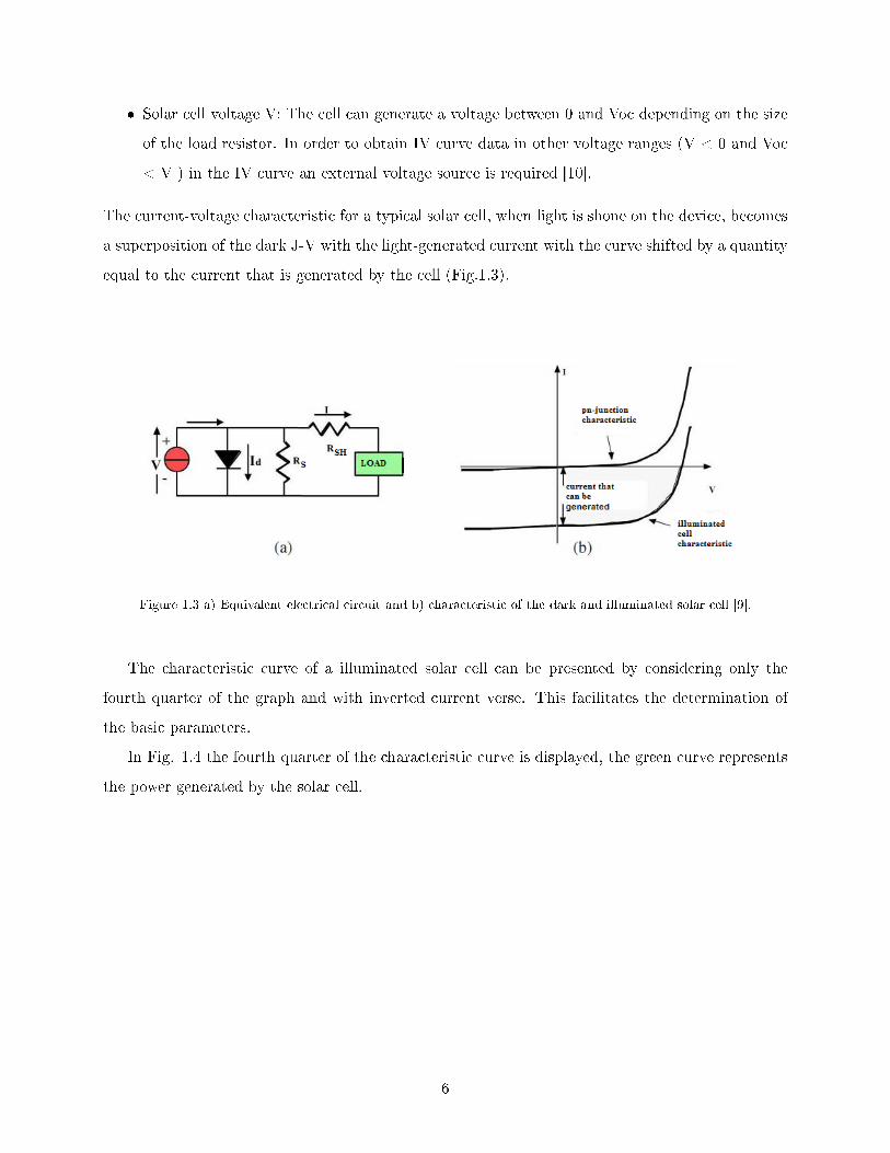
Fig. 1.3 shows an equivalent circuit model which is commonly used to interpret the characteristic
of PV devices. The solar cell in the dark acts as a simple diode: the current-voltage relationship
4
follows the exponential relation of the pn-junction:
J(V ) = J0(eqV/AkT − 1)
Eq. 1.1
where k is the Boltzmann constant, T the temperature, V is an external applied bias voltage,
J(V) the current density, A the diode quality factor and q the elementary electric charge (J(V) is
obtained by dividing the current to the device area) [9].
For a better description of a real device, resistive losses have to be added into this equation: A
series resistance RS and a shunt resistance RSH. Additionally, a photo-generated current density
JL has to be introduced into the equation to describe the device under illumination (in the dark
JL =0). In thin �lm solar cells, JL may depend on the applied bias voltage. The so-called 1-diode
model describing the current-voltage characteristic of a solar cell is given by the following equation:
J(V ) = J0
[exp(
q(V −RSJ(V ))
AkT)− 1
]+V −RsJ(V )
Rp− JL
Eq. 1.2
where J(V) accounts for the current density �owing through the device which is the sum of
the current density �owing through the diode (�rst term), the current density �owing through the
parallel resistance (second term) and the photo-generated current density (last term) [10].
The illuminated cell behavior can be related to that of a diode parallel connected with a current
source RS, these connected in series with a shunt resistance RSH.
� The diode D takes into account the current losses due to recombination in the interior of the
cell. D has an ideality factor n and a saturation current I0 (current in the dark at reverse
bias);
� The current source is equivalent to the photo generated current due to the PV e�ect IL;
� RS takes into account all the resistances at interface in the layers, the conductivity of the
semiconductors, and the electrodes;
� RSH takes into account the leakage of the current through shunts as a result of defects in the
�lms. (For good performance of the OPV device, Rs needs to be low and Rsh to be high);
5
� Solar cell voltage V: The cell can generate a voltage between 0 and Voc depending on the size
of the load resistor. In order to obtain IV curve data in other voltage ranges (V < 0 and Voc
< V ) in the IV curve an external voltage source is required [10].
The current-voltage characteristic for a typical solar cell, when light is shone on the device, becomes
a superposition of the dark J-V with the light-generated current with the curve shifted by a quantity
equal to the current that is generated by the cell (Fig.1.3).
Figure 1.3 a) Equivalent electrical circuit and b) characteristic of the dark and illuminated solar cell [9].
The characteristic curve of a illuminated solar cell can be presented by considering only the
fourth quarter of the graph and with inverted current verse. This facilitates the determination of
the basic parameters.
In Fig. 1.4 the fourth quarter of the characteristic curve is displayed, the green curve represents
the power generated by the solar cell.
6

Figure 1.4 Current-voltage characteristic for a generic illuminated solar cell. [9].
J�V characterization means determination of the basic parameters: the open circuit voltage
VOC, the short-circuit current JSC, the �ll factor FF, and e�ciency (h) which are determined by
only three points on the J�V curve and are brie�y described below.
1.2.2 Power conversion e�ciency
The power conversion e�ciency (PCE) of a solar cell is de�ned as:
PCE =JSC × VOC × FF
Pin
Eq. 1.3
where JSC is the short circuit current density, VOC is the open circuit voltage, FF is the �ll
factor and Pin is the power of the incident light [10].
1.2.3 Fill factor
The �ll factor describes the �squareness� of the J-V curve. It is the ratio between the maximum
product of J and V and the product VOC and ISC.
7

Fill factor =Jm × VmJSC × VOC
Eq. 1.4
thus
Pmax = (JV ) = VOC × JSC × FF
Eq. 1.5
where Jm and Vm are the maximum power point current density and voltage, respectively [10].
The higher the FF the more the J-V characteristics resembles a constant current source with a
maximum voltage and the higher is the electric power that can be extracted. The voltage-current
(Vp, Ip) combination that gives the largest power rectangle is called the maximum power point.
Due to physical constraint on diode quality, the practical limit to the �ll factor is less than the
ideal value of 1 [4].
1.2.4 Open circuit voltage
VOC can than be derived quantitatively using:
VOC =nkT
qln(
ILI0
+ 1)
Eq. 1.6
In contrast to silicon p-n junction solar cells, the origin of the open circuit voltage in bulk
heterojunction devices is still not completely understood. Multiple reports have investigated this
property for OPV devices. In 2001, Brabec et al. [11] proposed an e�ective band gap model for bulk
heterojunction cells, whereby the maximal value of VOC is related directly to the energy di�erence
between the HOMO level of the donor and the LUMO level of the acceptor.
In 2006 a report studied the relationship between the energy levels of the donor-acceptor blend
and the VOC for bulk heterojunction devices [12]. It was found that there exists a linear relationship
8

between the HOMO position, which is related to the band gap of the heterojunction, and the VOC.
This relationship between the HOMO of the donor material and the VOC of the device was found:
VOC = (1
e(∣∣EDonorHOMO
∣∣− ∣∣EAcceptorLUMO∣∣)− 0.3V
Eq. 1.7 [4]
1.2.5 Short circuit current density
The short circuit current density JSC is the maximum photocurrent density which can be extracted
from the device at short circuit conditions.
The JSC is directly related to the external quantum e�ciency (EQE), which is de�ned as the
ratio between the number of electrons on the external circuit and the number of incident photons
at a speci�c wavelenght.
JSC can be expressed as [4]:
JSC =q
hc
∑ ˆ λmax
λminEQE × Pin(λ)λ× dλ
Eq. 1.8
For the operation of a hybrid solar cell, EQE is dependent on �ve major steps, each of which has
some associated e�ciency. Thus, it can be expressed as [4]:
EQE = ηabs × ηdiff × ηdiss × ηtr × ηcc
Eq. 1.9
9

Figure 1.5 Energy band diagram illustrating the �ve steps in the charge transfer process. The e�ciency of these
steps determines the EQE of the hybrid device [4].
The parameter habs describes the absorption yield of the device, which is displayed as (1) in
the Fig. 1.5. The absorption spectrum of the material is determined by both the band gap and
absorption coe�cient of the material, whilst the thickness of the photoactive layer will also a�ect
the absorption yield [13].
The parameter hdi�, displayed in Fig. 1.5 as (2), describes the ability of an exciton to di�use to
a donor-acceptor interface. This parameter depends on both the excitonic di�usion length, which is
a material property, and the distance between excitation and the nearest interface, which is related
to the nanoscale design of the photoactive layer. As the excitonic di�usion lenght in conjugated
polymers is very low [14], control over the D-A morphology is important for successful exciton
di�usion.
The parameter hdiss, displayed in the Fig. 1.5 as (3), is the exciton dissociation yield. The energy
o�set, required to allow conduction to occur, must be larger than the excitonic binding energy in
the material to facilitate charge transfer. This energy is typically in the range of 0.1-0.5 eV [14].
The parameter htr(4) describes the e�ciency of charge carrier transport throughout the device.
The parameter hccdescribes the e�ciency of charge collection at the electrodes. This represents
the ability of the charge carriers to be injected into the electrodes from the photoactive layer. The
success of this step is dependent on the electronic composition of the device.
10

2 Materials
The choice of materials in OPV is crucial to the overall e�ciency and thus the success of this
technology. This section describes the materials which have been used in this research work and
their respective functions in the solar device. The solar cell structure used in this work is of an
inverted type, where the cathode is the transparent front electrode and the anode the back electrode.
The complete structure of the solar cell investigated in this work is:
Zinc oxide doped with aluminum as front electrode, zincphthalocyanine mixed with Buckminster
carbon fullerene as photoactive layer, molybdenum oxide as intermediate bu�er layer and silver
contacts as back electrodes.The device is built on a glass substrate.
The mixed layer of ZnPc and C60 deposited in this experimental work presents an aggregation
of small grains of both donor and acceptor contacting materials with dimensions below the excitons
di�usion lenght.
Figure 2.1 Schematic bulk heterojunction structure for the inverted solar cell used in this work.
2.1 Substrate and front electrode
Glass is by far the most reported substrate because of its low cost and stability in almost any
subsequent treatment and was therefore chosen as substrate.
With respect to the transparent electrode, ITO has been the almost exclusive choice, given
its excellent properties as hole conductor, but due to the scarcity and the cost of indium, which
11
by weight is the main material in ITO, the need for new transparent semiconducting materials is
growing.
In this work, a zinc oxide layer doped with aluminium is used as a low work function window
cathode. The function of the cathode is to collect electrons from the device and here contributes
as well to the device stability, as oxygen and water molecules are blocked by the ZnO:Al layer
[4]. When doped with aluminium ZnO is a n-type contact. ZnO can be formed using a variety of
synthesis methods and exhibits high electron mobility; furthermore it has a proven suitability of
forming structurally well-de�ned hybrid structures with various conjugated organic molecules [15].
2.2 The intermediate layer
Absorber/electrode interfaces in OSC are optimized either by the electrode surface treatments or,
as in this work, by insertion of an intermediate or bu�er layer [16].
The intermediate layer has the function to selectively transport one type of charge (negative or
positive) while simultaneously blocking the opposite charge, decreasing in this way the probability
of charge recombination.
Furthermore, intermediate layers are used to bridge a mismatch of energy levels between the
active layer and an electrode, improving in this way the alignment of the energy levels. The in-
termediate layer even compensates for the roughness that electrodes have and that might result in
shunts in the �lm, removing some of the shunts. The intermediate layer used in this work follows an
anode and is thus used as hole conductor and electron blocking layer. As hole conductor the most
widely used electron-blocking material has been polyethylenedioxythiophene:polystyrenesulfonate
(PEDOT:PSS) but the substitution of PEDOT:PSS with stabler materials can signi�cantly improve
the device´s stability. In this work a hole conductor bu�er layer of MoO3 has been used. This oxide
has been progressively investigated in the last years due to its supposed appropriate work function
values and band alignment when inserted between the photoactive layer and the electrode. It has
been in fact experimentally found that molybdenum oxide as the interfacial modi�cation layer in
OSC improves the transport mechanism of the solar cell [17].
Recently, transition metal oxides, such as molybdenum oxide MoO3, vanadium oxide V2O5, and
tungsten oxide WO3 have attracted much attention for organic solar cells application due to their
suitable electronic properties and charge generation ability for organic solar cells. Recent works
[36,37] reported how the presence of MoO3 layer at the organic/metal interface signi�cantly reduces
the contact barrier and provides protection from di�usion and other chemical reactions between the
12

organic layer and the metal.
MoO3 presents highly e�cient charge injecting (or extracting) properties, improved stability,
high transparence and compatible easy- fabrication process (thermal evaporation) and therefore has
been here chosen as intermediate bu�er layer.
Furthermore the oxide �lms of MoO3 can be deposited by thermal evaporation, which is com-
patible to thermal evaporation of Au anode, used in this experimental work [38].
In this work the work function energy levels of the MoO3 at the interface with the organic layer
is investigated. In fact, despite numerous papers related to the application of transition metal oxides
as bu�er layer in organic electronic devices, the underlying physical mechanisms pertaining to their
electronic structure remain not completely de�ned.
2.3 The active layer
The active layer used in this work consists of a bulk heterojunction of buckminster fullerene C60 as
acceptor material and zinc phthanolocyanine (ZnPc) as the donor material.
2.3.1 Fullerene
The fullerene's role as an electron acceptor and in providing a continuous network for electron
transport in polymer and small molecules blend devices is well established [18].
This molecule is very stable and can be easily evaporated in vacuum conditions. The absorption
coe�cient a of C60 is 0.8·105 cm-1. C60 is considered an optimal acceptor material for organic solar
cell due to its high acceptor properties [8]: the transport of an electron from a donor molecule next
to a C60 molecule takes place in about 40 fs [8].
2.3.2 Donor material
Phthalocyanine (ZnC32H12N8) Fig.) has been used as photoactive donor material. ZnPc molecules
are easy and cheap to synthesize. ZnPc has an absorption coe�cient a of up to 1.5·105cm-1, being
thus an optimal absorber material in the visible region, from 550 to 750 nm [8]. The molecules are
small and stable enough to be thermally evaporated. The hole mobility m of ZnPc is about 0.02
cm/Vs, the molecules are considered as p-conductor.
13

Figure 2.2 Chemical structure of (a) zinc phthalocyanine and (b) fullerene C60 [8].
2.4 The back electrode
The back electrode is the �nal layer that completes the device structure. Similar to the front
electrode, the use of high or low work function metals de�nes the operation of the back electrodes
as anode or cathode, respectively. The electronic properties of the latter electrode must match with
those of the organic absorber layer. Particularly, for an e�ective collection of the charge carriers
from a single organic layer, the work function of the metallic is adjusted to the HOMO/LUMO
level of the donor/acceptor material for the formation of an ohmic contact. In the case of absorbers
from blend structures e�ective charge-selective electrodes are required. These are achieved by the
�ne adjustment of the electrode work function by allowing low and high work function conducting
materials. Depending on the desired work function of the back electrode, di�erent metals are use.
Aluminium, silver and gold are the most commonly used. Here physically deposited silver contacts
are used.
2.5 Final structure
A schematic overview of the complete solar cell, with inverted structure, used and investigated in
this work is presented in Fig. 2.3.
In an inverted cell, the electric charges exit the device in the opposite direction as in a normal
device. The positive and negative electrodes, which absorb the negative and positive charges, re-
spectively, are reversed. Inverting the device architecture allows to make the cathode out of a more
suitable material, which can provide e�ective protection to the polymer layer. [19].
14

Figure 2.3 Schematic overview structure of the solar cell with ZnPc and C60 as photoactive layer. The investigated
interface is shown.
15

3 Surface characterization techniques
Photoelectron spectroscopy (PES) is a surface sensitive investigation method and one of the most
useful technniques of modern surface material science. This technique is based on the photoelectric
e�ect discovered by Heinrich Hertz in 1887 [20]. A photon transfers its energy to the atom thus
exciting electrons to upper energy levels, from which they can be ejected from the material. From
the energy distribution of the photoelectrons, which is probed in an electron energy spectrometer,
the fundamental energy levels and excitation energies of the atoms in a sample are determined.
Di�erent energy ranges provide di�erent information: electrons emitted from core levels furnish
information about the presence and, to a certain degree, the concentration of elements in the sample.
Furthermore, the chemical environment can also be determined, i.e. the oxidation state of the
element in question and as well as its �rst coordination shell may also be determined from the
spectra. Electrons from valence levels give information about the electronical band structure of the
material.
Photoelectron spectroscopy requires vacuum operating conditions. The electrons emitted from
the sample should meet as few gas molecules as possible on their way to the analyser so that they
are not scattered and thereby lost from the analysis. Furthermore these techniques are higly surface-
speci�c, with sampling depths tipically of a few atom layers. Most of the electrons originate from
the �rst atom layers. Even very small amounts of contamination can a�ect the experiment. Since
the principal source of contamination comes from the residual gas in the operating chamber, the
system must operate under ultra-high vacuum (UHV) conditions. In fact a monolayer of gas will
accumulate on a surface in about 1.5 s at a pressure of 10-6 torr and at room temperature, if every
molecule hitting the surface stays there on impact. If, as typical requirements, no more than 0.05
atom layers of contaminant should accumulate in the space of 30 min, then, gas kinetics rule that
the residual gas pressure should be 4 �10-11 torr.
Furthermore UH vacuum is needed to extend the life of X-ray and electron optics in the vacuum
system.
3.1 UPS
Low energy photons may be used to excite electrons in the solid. In ultra-violet photoelectron
spectroscopy (UPS) the source of photons is a di�erentially pumped inert gas discharge lamp. This
produces discrete low energy resonance lines: He I 21.2 eV, and He II 40.8 eV. Since there is only
16

su�cient energy to emit electrons from the valence band, the technique is used in the study of the
electron band structure of solids and not for analytical studies.
3.2 XPS
X-ray photoelectron spectroscopy is a surface chemical analysis technique, also referred to electron
spectroscopy for chemical analysis (ESCA), used to analyze the surface chemistry of a material in
its �as received� state and can be addressed to a wide variety of samples. XPS was developed in the
mid-1960's by Kai Siegbahn and his research group at the University of Uppsala, Sweden.
XPS detects all elements with an atomic number Z of 3 and above.
Surface analysis by XPS is performed by irradiating a sample, in a vacuum environment, with
monochromatic soft X-rays. They interact with the inner-shell electrons of an atom in the surface
region of the material of about 1-10 nanometers by the photoelectric e�ect and cause electrons to be
ejected. The kinetic energy of the emitted photoelectrons provides information about the binding
energy of the electron in the material. The basic equation of XPS is
Ek = hv −BE − φs
Eq. 3.1
where hv is the energy of the incident photon (h is the Planck's constant and v the X-ray frequency),
BE is the binding energy of the atomic orbital from which the electron originates, and φs is the
spectrometer work function, which is found by calibration [20].
The kinetic energy Ek of the photoelectron is measurable then the binding energy BE can be
calculated. XPS spectra represents the intensities of the photoelectrons versus BE or Ek. Since
each element has a unique binding energy, the energy of the photoelectrons is related to the atomic
and molecular environment from which they originated. The number of electrons emitted is related
to the concentration of the emitting atom in the sample.
X-rays are created by accelerating high energy electron beam (~15keV) onto an anode material
(typically Mg and Al). The electron beam creates holes in the core level of the anode material and
electrons from outer shells �ll up the holes emitting characteristic X-ray radiation. If Mg is used as
anode material the created X-rays (Mgka) have an energy of 1253.6 eV, while with Al, the radiation
(Alka) has an energy of 1486.6 eV.
17

The relaxation of the excited state due to photoemission, can occur via emission of radiation
(�uorescence radiation) or by emission of an additional electron (Auger electrons). In this process,
as shown in Fig. 3.1 , an outer electron falls into the inner orbital vacancy, and a second electron
is emitted, so that the Auger electron has kinetic energy equal to the di�erence between the energy
of the initial ion and the doubly-charged �nal ion. Since the Auger process contains three steps,
the kinetic energy of the Auger electron depends only on those thress electronic levels and not on
incident X-ray photon energy.
The electron signal in XPS includes contribuitions from both photoelectron and Auger electron
lines.
Figure 3.1 Diagram of the photoelectric process (top) and the Auger process (bottom) [21].
The information depth in XPS is related to the distance an electron can pass through the matter.
This average distance that an electron can travel between successive impacts without modifying
its direction or energy or other particle properties is called the inelastic mean free path of an electron.
The probability of interaction of the electrons with matter far exceeds those of the photons, so
while the path lenght of the photons is of the order of micrometers, that of the electrons is of the
order of tens of angstroms. Thus, even if ionization occurs to a depth of a few micrometers, only
those electrons that originate within tens of angstrom below the solid surface can leave the surface
without energy loss. It is these electrons that produce the peaks in the spectra and are useful for
18

the analysis. The inelastic mean free part l of the electrons in the regime between a few eV and
many hundred eV is plotted in Figure 3.2. The dashed curve shows a calculation of the inelastic
mean free path independent of the material and the points are measured data from many elemental
solids. The data points scatter more or less around the calculation. The curve is therefore often
called a universal curve. The reason for this universality is that the inelastic scattering of electrons
in this energy range is mostly involving excitations of conduction electrons, which have more or less
the same density in all elements. The mean free path curve has a minimum around a kinetic energy
of about 70 eV. There the mean free path is less than 10 Å. This means that a detected electron
with this kinetic energy which has left the solid without su�ering an inelastic scattering event must
originate from the �rst few layers.
Figure 3.2 The mean free paths of the electrons in solid [21].
3.3 Synchrotron
A further source of photons used for spectroscopy analysis is the synchrotron radiation. Synchrotron
radiation is an electromagnetic radiation emitted from de�ected charged particles moving at rela-
tivistic velocities.
Classically, any charged particle which moves in a curved path or is accelerated in a straight-
line path emits electromagnetic radiation. Various names are given to this radiation in di�erent
19
contexts, in the application to circular particle accelerators like synchrotrons, where charged particles
are accelerated to very high speeds, the radiation is referred to as synchrotron radiation. Electrons
circulated continuosly in a storage ring (BESSY II, Berlin) produce a continuous spectrum of photons
with energies from few electronvolts to several kiloelectronvolts [20]. With a monochromator a
variable energy photon source is provided. As a consequence of relativistic motion, the radiation is
emitted in a narrow cone in the forward direction from a point like source. At BESSY II, Berlin,
the electron's energy is 1.7 GeV and synchrotron radiation is generated from magnetic de�ections
in simple electromagnetic bending magnets, from undulators consisting of long magnetic rows of
permanent magnets as well as from superconducting magnet structures like wavelength shifters and
multipole wigglers.
Synchrotrons consist of large circular magnets positioned around the circumference of the circle.
Magnets ensure that the electrons may circle in the storage ring. The main components are the
dipoles, the quadrupoles and the sextupoles. The dipoles enable the circular orbit of the electrons.
The quadrupoles compensate the natural behavior of electrons to drift apart. Sextupoles make small
corrections on the quadrupoles and are important for storing the beam over a longer period of time.
Acceleration of the charged particles is achieved by the application of radio frequency electric
�elds at rf (radio-frequent) cavities along the circumference of the ring. The magnetic �elds must be
increased synchronously with the acceleration in order to keep the particles on the constant radius
path.
The accelerators can be used with protons, electrons and even with heavier positive ions.
For surface chemical analysis electrons are used because they are relatively easy to accelerate
due to their high electric charge and their small mass.
The energy radiated from the electrons is proportional to the fourth power of the particle speed
and is inversely proportional to the square of the radius of the path. It becomes the limiting factor
on the �nal energy of particles accelerated in electron synchrotrons.
The classical formula for the radiated power from an accelerated electron is
P =2Ke2a2
3c3
Eq. 3.2
which is the Larmor formula, used to calculate the total power radiated by a non-relativistic
point charge as it accelerates, where a is the acceleration, e is the charge, and c is the speed of light.
20
For a non-relativistic circular orbit, the acceleration is just the centripetal acceleration, v2
r .
The orbits of interest in accelerators are higly relativistic, so the relativistic acceleration can be
calculated from
a =1
m
dp
dτ=
1
mγd(γmν)
dt= γ2
dν
dt= γ2
ν2
r
Eq. 3.3
where τ = tγ= proper time,
γ =1√
1− v2
c2
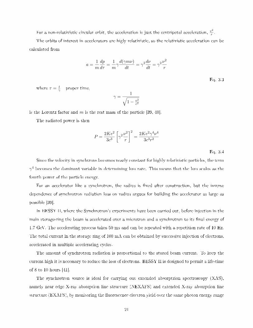
is the Lorentz factor and m is the rest mass of the particle [39, 40].
The radiated power is then
P =2Ke2
3c3
[γ2ν2
r
]2=
2Ke2γ4ν4
3c3r2
Eq. 3.4
Since the velocity in synchtrons becomes nearly constant for highly relativistic particles, the term
γ4 becomes the dominant variable in determining loss rate. This means that the loss scales as the
fourth power of the particle energy.
For an accelerator like a synchrotron, the radius is �xed after construction, but the inverse
dependence of synchrotron radiation loss on radius argues for building the accelerator as large as
possible [39].
In BESSY II, where the Synchrotron's experiments have been carried out, before injection in the
main storage-ring the beam is accelerated over a microtron and a synchrotron to its �nal energy of
1.7 GeV. The accelerating process takes 50 ms and can be repeated with a repetition rate of 10 Hz.
The total current in the storage ring of 100 mA can be obtained by successive injection of electrons,
accelerated in multiple accelerating cycles.
The amount of synchrotron radiation is proportional to the stored beam current. To keep the
current high it is necessary to reduce the loss of electrons. BESSY II is designed to permit a life-time
of 8 to 10 hours [41].
The synchrotron source is ideal for carrying out extended absorptrion spectroscopy (XAS),
namely near edge X-ray absorption �ne structure (NEXAFS) and extended X-ray absorption �ne
structure (EXAFS), by monitoring the �uorescence electron yield over the same photon energy range
21

in the region of the absorption edge.
The principle of NEXAFS measurements is the absorption of an x-ray photon by a core level of
an atom in a solid and the consequent emission of a photoelectron. The resulting core hole is �lled
either via an Auger process or by capture of an electron from another shell followed by emission of a
�uorescent photon. The di�erence between NEXAFS and traditional photoemission experiments is
that in photoemission, the initial photoelectron itself is measured, while in NEXAFS the �uorescent
photon or Auger electron or an inelastically scattered photoelectron may also be measured.
22

4 Experimental
4.1 Preparation of the samples
The samples used in this work were fabricated through the vapour phase deposition technique (VPD).
In this chapter the principles of the VPD will be brie�y described.
The samples were prepared on glass substrates coated with a transparent, conducting aluminum
zinc oxide layer with a sheet resistance of 5 W/2. The thickness of the ZnO:Al �lm was about 920
nm and was measured with a Dektak-Kontakt-Pro�lometer. The organic layers of ZnPc:C60, were
deposited by the OVPD (Organic Vapour Phase Deposition) technique and the molybdenum oxide
layer with the same VPD principle.
The following series of samples were prepared to study the interface between ZnPc:C60 and
MoOx.
� 2 x Glass/ZnO:Al
� 2 x Glass/ZnO:Al/ZnPc:C60
� 10 x Glass/ZnO:Al/ZnPc:C60/MoOx
� 2 x Glass/ZnO:Al/MoOx
The sample without the organic layer and/or the molybdenum oxide were studied as reference
samples.
The average thickness of the MoOx was approximately calculated about 100 nm. The SEM
characterization of the pro�le of MoOx on ZnO:Al images show an uniform and compact �lm of
MoOx(Fig. 4.1).
23

Figure 4.1 Scanning electron micrographs of the cross-section of physically deposited MoOx on ZnO:Al. Shown in
the �rst micrograph are the data used for evaluation of the thickness.
4.1.1 Organic layer deposition
The OVPD technique has been proved an useful method for the deposition of organic semiconductors
devices [22]. Currently the most common used technique for the deposition of thin (<100 nm),
molecular organic electronic devices is the vacuum thermal evaporation (VTE), which permits an
high degree of purity. However, control of thin �lm uniformity and the mixing of multiple compounds
into a single �lm, which is essential to the achievement of high performance devices, can be di�cult
using VTE, particularly for large-area substrates. In addition, in VTE a considerable fraction of
the evaporant coats the cold walls of the deposition chamber; over time, ine�cient materials usage
results in a thick coating which can �ake o�, leading to contamination of the system and substrate.
Thin �lms produced by OPVD do not have problems related to contamination from the particles
coming out of the walls of the chamber as they are warm and do not allow particles to stick. Due
to the presence of the carrier gas, that becomes saturated with the vapours of the organic materials
coming out from the source, the deposition occurs through an equilibrium process. VPD has been
recently demonstrated as an alternative technique that eliminates the limitations of the VTE thus
resulting in a rapid, particle-free, uniform deposition of organics on even large area substrates [23].
A schematic drawing of the OVPD method used in this work is shown in Fig. 4.2 [22]. The
system is based on the commercial OVPD principle described in [23]. However, whereas in the
OPVD system described in [23], the sources and the substrate are placed together into a hot wall
horizontal quartz tube, in the OPVD system used here, the sources and the deposition chamber are
24

separated. Moreover, the deposition chamber of the OPVD system is provided with a close coupled
showerhead with multiple ori�ces that acts as a gas distributor (Fig. 4.2). This allows an uniform
injection of the organic molecules over the entire deposition area. The organic materials used in this
work - ZnPc and the fullerene C60 - are thermally evaporated in special source containers in the
presence of a preheated inert gas, N2. The organic compounds are transported by the carrier gas
through the deposition chamber. The stream then uniformly passes through the showerhead and
condenses on the deposition area, consisting of a cooled substrate. Prior to their introduction in
the showerhead ori�cies, the organic compounds in the gaseous phase are homogenised in a mixing
chamber, being supplied from source containers mounted in separated furnaces. Each of the three
furnaces mounted in the actual desing of the OPVD system used in this work, can hold multiple
containers with di�erent source materials. The deposition rate can be changed by changing the gas
�ow rate through external mass-�ow controllers. Thus, the deposition runs can be performed at
di�erent source �ows keeping at the same time a constant N2 gas quantity, by adjusting the dilution
pipe. The pipes are heated and always kept under continuous N2 �ow. In standby conditions, the
sources are �lled with N2 and kept closed using valve B, while during the deposition process, valves
B are o� and valve A is open (Fig.4.2). Independently of the N2 total �ow, the deposition chamber
pressure can be varied between 10-1 and 103 mbar.
The organic materials used wew C60(MER Corp. Purity: 99,9%) and ZnPc (Alfa Aesar. Purity:
98%).
ZnPc:C60 layers were deposited at a deposition chamber pressure of 0,6 mbar. The source
evaporation temperature was <500°C and the showerhead temperature was set at 425°C. The organic
layer thickness was about 80 nm, the ratio 1:1 by thickness. The deposition rate was 0,483 Ang/s
.The N2 carrier gas quantity through each source (Qsource) was 500 ml/min and 283 ml/min for C60
and ZnPc respectively. Qtotal was 1150 ml/min. The substrate temperature was 132 °C, the source
temperature 436,7°C for C60 and 423,5°C for ZnPc. After the deposition process, the samples were
transferred from the OPVD system through a N2 �lled glove box.
4.1.2 Bu�er layer deposition
The bu�er layers of MoOx (Sigma-Aldrich, purity: 99,9%) were deposited with the same VPD
principle as described above.
2,2 g of MoOx powder were �rst put in the proper source container. In the deposition chamber
was set a pressure of 4,4 ;10-7mbar. The rate deposition, measured by a quartz microbalance, was
25

0.5 Å/s and the substrate temperature was kept at room temperature.
4.1.3 Silver contacts deposition
The Ag contacts were deposited in the high vacuum chamber (base pressure&10-7mbar) which is
directly attached to the OPVD chamber, without exposing the corresponding absorber/metal in-
terfaces to air. The high vacuum chamber is designed for deposition of solar cells metallic contacts
as well as for charging/discharging substrates or complete solar cell devices into/from the OPVD
system.
Further details about the OPVD setup can be found elsewhere [24].
Figure 4.2 Schematic drawing of the OPVD apparatus [28].
4.2 Optical measurements
Transmittance and re�ectance measurements were performed to monitor the band gap of the MoOx
layer. The optical spectra were taken for the bulk layer (100 nm). For thinner layers the performed
measurements were not taken into account because the interference e�ects were too high to allow a
signi�cant data interpretation. For carrying out these measurements, samples were redeposited on
quartz substrates due to the wider bandgap of glass.
Transmission and re�ection measurements were carried out between 250 and 2500 nm at 25°C
using a Perkin-Elmer Lambda 950 UV/Vis/NIR spectrometer in combination with an integrating
sphere in order to collect also the scattered light. Analysis of the re�ection and transmission data
were carried out for the evaluation of the absorption coe�cient a.
26
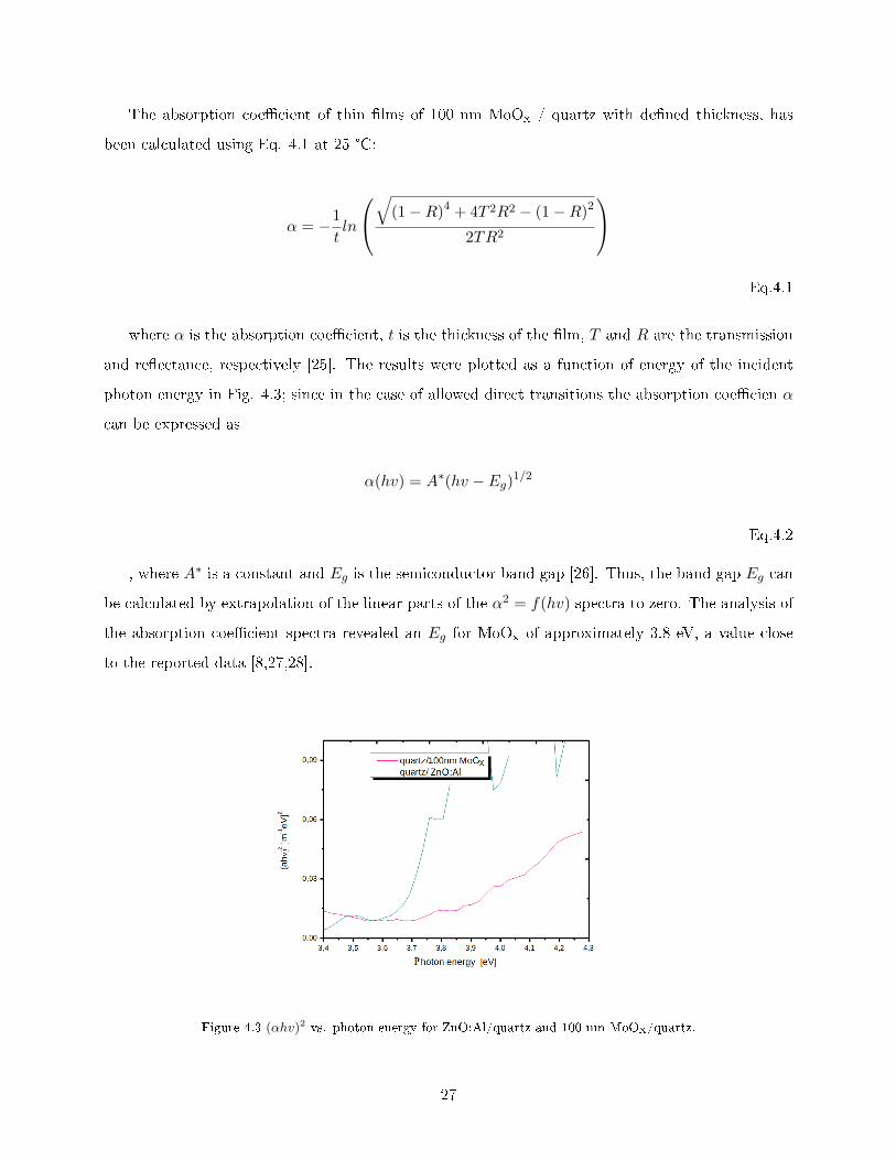
The absorption coe�cient of thin �lms of 100 nm MoOx / quartz with de�ned thickness, has
been calculated using Eq. 4.1 at 25 °C:
α = −1
tln
√(1−R)4 + 4T 2R2 − (1−R)2
2TR2
Eq.4.1
where α is the absorption coe�cient, t is the thickness of the �lm, T and R are the transmission
and re�ectance, respectively [25]. The results were plotted as a function of energy of the incident
photon energy in Fig. 4.3; since in the case of allowed direct transitions the absorption coe�cien α
can be expressed as
α(hv) = A∗(hv − Eg)1/2
Eq.4.2
, where A∗ is a constant and Eg is the semiconductor band gap [26]. Thus, the band gap Eg can
be calculated by extrapolation of the linear parts of the α2 = f(hv) spectra to zero. The analysis of
the absorption coe�cient spectra revealed an Eg for MoOx of approximately 3.8 eV, a value close
to the reported data [8,27,28].
Figure 4.3 (αhv)2 vs. photon energy for ZnO:Al/quartz and 100 nm MoOx/quartz.
27

4.3 Characterization at CISSY of the ZnPc:C60/MoOx interface
The chemical and electronic interface characterization of the physically deposited layers is studied
by means of photoelectron spectroscopy. The theoretical background of photoelectron spectroscopy
is further developed in chapter 3.
Because this technique is surface sensitive, to reach the ZnPc:C60 interface it is important to
study samples with di�erent thicknesses of the MoOx layer, prepared as previously described.
The photoelectron spectroscopy characterization was carried out in the CISSY setup (CIS for
CuInS2 and SY for synchrotron). The experimental setup at the CISSY endstation consists of an
analysis chamber containing the PES and the X-ray emission spectroscopy (XES) spectrometers, a
central chamber for preparation procedures, which allows the simultaneous connection of
preparation modules, a sample manipulator and a load-lock system for entry of the samples. The
CISSY apparatus can be used alone, but a connection to the synchrotron is also possible. The set
up is schematically presented in Fig. 4.4 and a view of the experimental setup is shown in Fig. 4.5.
Figure 4.4 Schematic diagram of the CISSY experimental end station.
28

Figure 4.5 Photo of the CISSY experimental station were photoelectron spectroscopy measurements have been
carried out.
Through the photoelectron spectroscopy electrons are emitted and detected by a detector, thus
a start energy value and an end energy value must be speci�ed to determine the energie interval
that the detector must measure. Other parameters to be speci�ed before the carrying-out of the
photoelectron spectroscopy are the number of the scans and pass energy. During the analysis the
number of the measured electrons is determined and shown as a spectrum.
After the measurements, the data are stored on the server and edited with the data analysis
software IgorPro.
4.3.1 Ultraviolet photoelectron spectroscopy
The band alignment at the interface between active and bu�er layer is an important aspect in thin
�lm solar cells. The transport mechanism of the device depends on the energy band alignment
and the work function values of the materials. Ultraviolet photoelectron spectroscopy (UPS) was
used in this work to determine the workfunction values and, together with optical measurements, to
determine the valence band o�set.
The work function is the energy that an electron at the Fermi level requires to leave the matter,
i.e. reach the vacuum level.
The work function was calculated by using the following formula:
29

ϕ = hv − Ek − Ef
Eq.4.3
where hv is the photon excitation energy, Ek the energy value at the secondary electron cuto�
(SECO) and Ef the energy of the Fermi level [21].
The position of the secondary electron emission line was determined by linear extrapolation of
the valence band spectrum at the high binding energy side. The intersection of the straight line
with the x-axis corresponds to the kinetic energy. Substracting these and the energy of the Fermi
level from the excitation energy of 21.22 eV the work function f is determined.
The valence band edge was obtained from the linear extrapolation of the valence band spectra
over the background level.
The valence band o�set at the interface of ZnPc:C60 and MoOx was estimated by combining the
results of optical measurements, carried out with the Perkin-Elmer UV-VIS spectrometer, and the
UPS analyses. For the determination of the Fermi level, a gold foil was used.
spazio
30

Figure 4.6 Ultraviolet photoelectron spectra for 0, 0.5 and 1 nm MoOx showing the valence band maximum. The
zero in the abscissa corresponds to the Fermi level which is obtained by measuring the Fermi edge of a gold foil with
UPS. The spectra are recorded using the UV radiation source of He I (hn=21.22 eV). In the inset the di�erence
between the Fermi level and the valence band values is shown.
4.3.2 X-ray photoelectron spectroscopy
XPS analyses were carried out with the aim of obtaining information about:
31

� Composition of the surface by identi�cation of all elements (except H and He) present at
concentrations > 0.1 atomic %;
� Oxidation state;
� Chemical shift: the binding energies of electrons in an atom are a�ected by the atom's chem-
ical environment, thus shifts in photoemission peaks may indicate a change in the chemical
environment of the element. This information is an useful tool to determine changes in the
oxidation state of the surface. In this case, the binding energy increases due to the fact that
part of the electronic density is transferred to the oxidizing species having higher electronega-
tivity values. As a result, the electronic density of the oxidized substance becomes unbalanced
against the positive nuclear charge;
� Auger signals: The reason for analyzing the Auger lines in photoemission spectrum is that the
Auger electrons are more sensitive to chemical shifts than the respective photoelectrons.In the
case of zinc compounds, the Zn photoemission lines may not show shifts in binding energy,
whereas the corresponding Auger lines can shift several electron volts. In determining the
chemical state of an atom, the evaluation of the so-called Auger parameter is a useful method.
The Auger parameter is de�ned as the combination of the photoelectron binding energy and the
kinetic energy of the related Auger electron. Many Auger parameters for known compounds
are listed in the literature [29]. Since the energy di�erence between photoelectron and the
related Auger electron of an element is �xed for a given chemical environment, any change in
Auger parameters can be attributed to a change in the chemical environment of this element.
In determining the elements of the sample, the position of the photoemission peaks are compared
with reference data available in the literature.
For the XPS analysis of the ZnPc:C60 and MoOx interface a sample series consisting of samples
with di�erent MoOx thickness was prepared by following the recipe explained in chapter 3.
The characterization of these samples gave a MoOx thickness resolved information on the com-
position of the layers. After the preparation the samples are kept under N2 environment to minimize
contaminations from air.
All XPS analyses were all performed in ultra high vacuum conditions.
The characterization was performed using MgKa and AlKa X-ray sources.
A survey spectrum is taken as a start analysis.
32

The XPS survey spectra taken with AlKa of the ZnPc:C60 and MoOx interface are shown in �g.
4.7, for 0.5, 1, 2, and 5 nm thin �lm MoOx layers. The main peaks present are Zn2p, Mo3d, C1s,
N1s, O1s, and Na1s.
Figure 4.7 XPS survey spectra of the ZnPc:C60 and MoOx interface for di�erent MoOx thicknesses.
The survey spectrum is a too coarse analysis for an accurate study of all the elements, thus for
every single element new settings are needed.
The peaks positions data of the elements, presented in the table below, are taken from the
literature database [29].
Table 4.1 Peaks positions of some spectral line of Zn, Mo, C, O and N [29].
Detailed spectra of Zn2p signal and ZnLMM Auger signals are shown in Fig. 4.8.
33

Figure 4.8 XPS spectra of the Zn2p signal for di�erent MoOx thicknesses. The energetic positions of the peaks are
shown.
A decrease of the Zn2p peak signal with increasing thickness of the MoOx layer can be observed.
The peak signal is only lightly present for the 2 nm MoOxsample and disappears for a thickness of
5 nm.
This means that the 2 nm thickness can be considered as the limit for a closed MoOx deposited
�lm on the organic layer.
The importance of the analysis of the zinc peak is related to the understanding of the morphology
of the MoOx layer. A compact oxide �lm is formed when no zinc peak is detected through the XPS
analyses. Iin this case up to a oxide thickness of 2 nm the deposition of the MoOx does not form
a closed �lm, thus the zinc coming from the layer below is still detected. For thicker �lms the zinc
peaks disappear, as it can be seen in Fig. 4.8, thus evidencing the compactness of the oxide layer,
that covers completely the organic layer.
No evident shift in the Zn2p peak position was detected (Fig. 4.9).
34

Figure 4.9 Zn2p peak position shift as function of the MoOx thickness.
The ZnLMM auger peaks are shown in Fig. 4.10. In order to assess the chemical environment of
the Zn atom at di�erent MoOxthicknesses, the energy positions of the ZnLMMpeaks are compared
with data extracted from literature [29].
The position of the ZnLMM peaks suggest that in the sample without the MoOx layer, the Zn
is embedded in the organic layer, whereas in the sample with the MoOx layer the Zn signal may
come from Zn bound to oxygen atoms. The Auger kinetic energy values, presented in Table 4.2,
show that the Zn signal, detected in the sample without the MoOx, comes from an organic bond
[29]. This means that the Zn detected in this layer is bound to organic molecules: in this case, the
molecules of the ZnPc. In the samples with the MoOx layer, on the other hand, the analysis of the
Auger kinetic energy's values reveals a zinc-oxygen bond, that is, a zinc atom tied to oxygen atoms.
All the Auger kinetic energy's values are taken from the Nist Database [29].
Figure 4.10 ZnLMM Auger peaks spectra.
35

Table 4.2 ZnLMM Auger peaks positions [29].
For the analysis of the oxidation state of the bu�er layer, the Mo3d peak signals for di�erent
MoOx thicknesses are studied.
Figure 4.11 XPS MoOx spectra of 0.5 to 10 nm of MoOx bu�er layer samples together with the reference sample of
100 nm MoOx.
The energetic positions of the MoOx peaks were compared with the data extracted from lit-
erature from the Nist Database [29]: MoO3: 232.3 eV~233.1 eV; 235.8 eV~236.41 eV for di�erent
molybdenum oxides: the position of the peaks corresponds to that of MoO3 in most of the literature
data and some to MoO2. Due to the fact that the literature data are taken from experimental
measurements, the biggest probability is that the oxide present at the surface is a MoO3.
Detailed peaks of the C1s, O1s and N1s signals are presented in Fig. 4.12.
36

Figure 4.12 XPS detailed spectra of C1s, O1s and N1s peaks signals.
37

The carbon signal shown in Fig. 4.12 comes from the organic layer in the case of thin �lms up
to 2 nm, where the thickness is still small enough to allow the detection of the carbon from the
organic layer. In the case of thicker �lms the carbon signal comes from the carbon present as surface
contamination, coming from the apparatus, and not anymore from the organic molecules. The peak
signal in this last case is less evident than the thinner �lms. This explains the peak shift detected in
the spectra of the carbon peaks. For intermediate thicknesses, the carbon signal is in�uenced both
by the carbon of the organic bounds and that of the contamination: the thicker the MoOx layer is,
the bigger is the contamination in�uence.
The N1s photoemission peak comes from the organic molecules of ZnPc, which contains atoms of
N (formula ZnC32H12N8). The energetic position of the N1s peak with increasing thickness remains
almost constant (Fig. 4.12), thus no chemical environment change takes place, but a change in the
form of the peaks is to observe. In comparision with the sample without the MoOxlayer, the other
peaks have a bigger area. This correlated with the formation of new nitrogen bonds. Thus it can be
expected that the molecules of ZnPc in contact with the phyisically deposited MoOx change their
type of bond.
The Mo3d peak area increases from 24.48 at room temperature to 30.17 at 200 °C
4.4 Temperature dependent J(V) measurements
The temperature dependent J-V measurements were performed on samples with an area of 0.2994
cm2 inside a cryostat which has a transparent window allowing the light to pass through.
The aim of the thermal treatments is the study of the in�uence of the temperature on the
ZnPc:C60/MoOx hybrid interface. In particular, the surface work function (WF) of the MoOx thin
�lms on ZnPc:C60 are here considered, as the WF parameter is a key step for the understanding
and the possible optimisation of the electron properties of the hybrid interface.
The temperature range of the measurements was from room temperature up to 320°C with the
following temperature steps: room temperature, 60°C, 80°C, 100°C, 120°C, 140°C, 160°C, 200°C,
240°C, 260°C, 280°C, 320°C. For each temperature the sample was annealed for 10 minutes.
To cool down the sample and ensure reaching of room temperature before each new temperature
step, the sample was kept in contact with a cold conductive substrate for 5 min after each annealing
step.
For switching from dark to illuminated measurement, a shutter on the transparent window is
used. In order to record J(V) curves under di�erent illumination intensities, a rotating wheel is
38

located between the halogen lamp and the shutter. The wheel has twelve di�erent �lters. One of
them is totally transparent providing an illumination intensity of Iilu = 1, approximately AM 1.5
[31].
The transparency of the �lters decreases from the �rst to the last one. In this manner, at a
given temperature, a J(V) curve is recorded �rst in the dark by closing the shutter, then the shutter
is opened and J(V) curves are recorded under di�erent illumination intensities, by means of the
rotating �lter wheel.
A direct relationship between short-circuit current density and the open-circuit voltage can be
obtained by writing the equation 1.2 [10] at short-circuit condition ( J(VOC) = 0 ).
JSC = J0
[exp
(qVOCAkT
)− 1
]+VOCRP
Eq.4.4
where the photogenerated current density is assumed to be the short circuit density. The current-
voltage curves JSC(VOC) measured under di�erent illumination intensities for a given temperature
provide di�erent points of the equation 4.4.
4.5 Temperature dependent photoelectron spectroscopy analysis
After carrying out of the J-V measurements as function of the substrate temperature, the ZnPc:C60/MoOx
interface behaviour during the thermal treatments was investigated by UPS and XPS measurements.
To allow a relation between the two analyses, the PES experiments were carried out with the same
annealing conditions as the J-V measurements.
The sample analyzed in this investigation step had the same structure of the complete solar
device characterized by J-V analysis. The ambient and temperature conditions were kept the same.
Annealing up to 320°C with the same temperature steps as the J-V analysis were reproduced in
the photoelectron spectroscopy apparatus. A cooling of the sample after each annealing step was
carried out to reproduce the same annealing procedure as for the J-V measurements.
A schematic graph of the annealing procedure is displayed in Fig. 4.13.
39

Figure 4.13 Graph of the annealing procedure.
The VB level was studied by analyzing the UPS spectra. Fig. 4.14 shows the UPS lines of the
sample ZnO:Al/80 nm ZnPc:C60/5 nm MoOx in the VB range. In the graph are displayed also the
spectra recorded during the thermal treatment.
40

Figure 4.14 UPS spectra recorded during the annealing and after the cooling down for the sample ZnO:Al/ 80 nm
ZnPc:C60/ 5 nm MoOx. Temperature values from room temperature to 200 °C are shown.
The VB position does not show any signi�cant variation with the annealing temperature.
For the determination of the work function the UPS spectra in the region of the secondary
emission line are considered. Fig. 4.15 shows the secondary emission lines for the annealed samples,
where intermediate spectra recorded during the thermal treatments are also displayed.
Figure 4.15 UPS spectra in the region of the secondary emission curve for di�erent temperatures of the annealing
process for the sample ZnO:Al/ 80 nm ZnPc:C60/ 5 nm MoOx. Shown are also the spectra recorded during the
thermal process.
41

In Fig. 4.16 detailed spectra of the main photoemission peaks C1s, O1s, Na1s and Zn2p recorded
by XPS for the ZnO:Al/ 80 nm ZnPc:C60/ 5 nm MoOx sample are shown.
Figure 4.16 XPS detailed spectra of the C1s, O1s, Na1s and Zn2p photoemission peaks for a 5 nm MoO3 sample at
room temperature before the annealing procedure (blue), after the annealing procedure (light blue), annealed at
160°C (orange) and 200°C (red).
The carbon peak signals after annealing are of lower intensity.
This could be due to the evaporation of the carbon impurities present on the surface of the
samples. Some carbon in form of oil in fact may be present at the cold sample surface. Due to the
annealing procedure up to 200°C evaporation from the surface occurs, rendering the other elements
signal peaks more visible to the detector. The carbon peak is the only one that through the annealing
procedure decreases in intensity, while O1s, Na1s and, less evidently Zn2p, become more intense (Fig.
4.15).
The increase of Zn2p with the annealing can be related also to di�usion of the Zn in the direction
of the MoOx layer, evidencing the Zn2p peak signal.
Since the Zn2p energy position is the same as before the annealing, new Zn bonds can be excluded.
The increase of the Na1s signal could be related with a thermal di�usion of this element, as for
the Zn2p. The Na source can be the glass substrate.
42
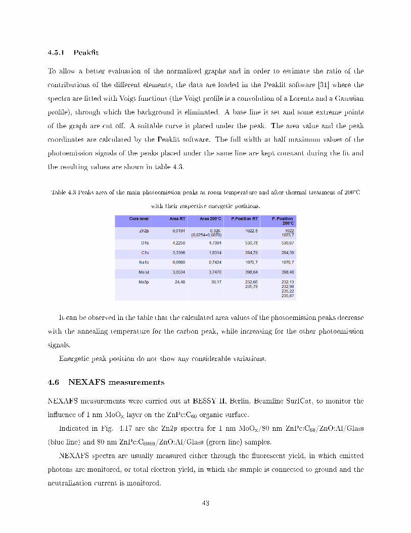
4.5.1 Peak�t
To allow a better evaluation of the normalized graphs and in order to estimate the ratio of the
contributions of the di�erent elements, the data are loaded in the Peak�t software [31] where the
spectra are �tted with Voigt functions (the Voigt pro�le is a convolution of a Lorentz and a Gaussian
pro�le), through which the background is eliminated. A base line is set and some extreme points
of the graph are cut o�. A suitable curve is placed under the peak. The area value and the peak
coordinates are calculated by the Peak�t software. The full width at half maximum values of the
photoemission signals of the peaks placed under the same line are kept constant during the �t and
the resulting values are shown in table 4.3.
Table 4.3 Peaks area of the main photoemission peaks at room temperature and after thermal treatment of 200°C
with their respective energetic positions.
It can be observed in the table that the calculated area values of the photoemission peaks decrease
with the annealing temperature for the carbon peak, while increasing for the other photoemission
signals.
Energetic peak position do not show any considerable variations.
4.6 NEXAFS measurements
NEXAFS measurements were carried out at BESSY II, Berlin, Beamline SurICat, to monitor the
in�uence of 1 nm MoOx layer on the ZnPc:C60 organic surface.
Indicated in Fig. 4.17 are the Zn2p spectra for 1 nm MoOx/80 nm ZnPc:C60/ZnO:Al/Glass
(blue line) and 80 nm ZnPc:C6060/ZnO:Al/Glass (green line) samples.
NEXAFS spectra are usually measured either through the �uorescent yield, in which emitted
photons are monitored, or total electron yield, in which the sample is connected to ground and the
neutralization current is monitored.
43

Fluorescence (thick line) and sample current (thin line) analyses were carried out, �uorescence
analysis has a deeper information sensitivity.
While the �uorescence curves in the two cases present almost the same trend, an evidently
di�erent signal is detected in the case of the sample current analysis, showing that a modi�cation
or interaction occurs in the �rst atom layers of the sample with the 1 nm MoOx, thus evidencing
how 1 nm MoOx layer has an in�uence on the surface.
Further analyses would be required to allow for a complete NEXAFS characterization, these
techniques need in fact many di�erent reference analyses due to the lack of complete literature
references.
The performed NEXAFS characterizations are the �rst step are the �rst stepof a promising
direction of investigation for a detailed understanding of this interface.
Figure 4.17 NEXAFS spectra of the Zn2p in the range 1015 eV-1040 eV for 1 nm MoOx/80 nm
ZnPc:C60/ZnO:Al/Glass and 80 nm ZnPc:C60/ZnO:Al/Glass samples.
From the spectra shown in Fig. 4.17 informations about the in�uence of 1 nm MoOx �lm presence
on the organic surface are taken.
It is clearly visible in these spectra that the samplecurrent signals present a di�erence between
the sample with and without the nanolayer of MoOx. This indicates that even a very thin �lm of 1
nm MoOx is able to induce a modi�cation on the organic surface thus resulting in di�erent peak's
44

signals. While a detailed comprehension of the peak's signals would require a further study, here it
can be concluded that NEXAFS analyses are a succesfull method for the investigation of this hybrid
interface, in particular the samplecurrent signals, because they are more surface sensible than the
�uorescence signals. They in fact allow an investigation at a minor depth of the interface than the
�uorescence studies.
45

5 Discussion and conclusions
5.1 Band alignment from UPS analysis
The work function results obtained with the UPS measurements are presented in Fig. 5.1.
The work function values derived from the UPS analysis for the MoO3/ZnPc:C60 interface are
(an error margin of 0.05 eV is considered): f=4.12±0.05 eV for the reference sample without organic
layer, f=4,65±0.05 eV for the 0.5 nm MoO3/ZnPc:C60 sample, f=4,82 ±0.05 eV for the 1 nm
MoO3/ZnPc:C60 sample, f=4,85 ±0.05 eV for the 2 nm MoO3/ZnPc:C60 sample, f=4,88 ±0.05 eV
for the 5 nm MoO3/ZnPc:C60 sample and f=5.22 ±0.05 eV for the 10 nm MoO3/ZnPc:C60 sample.
The reference sample with 100 nm MoO3 has a f=5.30 ±0.05 eV. Measurements have been carried
out at two di�erent positions on the sample, to monitor the uniformity of the thin �lm.
The work function values were determined from the UPS spectra, from the position of the
secondary electron emission line, as explained in the subsection 4.3.1.
Figure 5.1 Work function values in function of the MoOx thickness for two positions on the sample. The margin
error of 0.05 eV is indicated.
Kelvin probe force microscope (KPFM) measurements from literature data, were taken into
account to have a comparision with the UPS analysis carried out in this work. In table 4.3 data of
46

both the techniques are presented. KPFM is a scanning probe technique used to measure surface
potentiometry (the di�erence in electrode potentials measurement) of a �lm. The KPFM operates in
tapping mode, in a similar way to atomic force microscope (AFM), however, the tip-sample distance
is increased. This separation makes the oscillations sensitive to long range electrostatic forces. The
gradient of such forces is related to the potential di�erence between the tip of the microscope and the
sample [4]. Unlike STM (scanning tunneling microscope), this technique measures an electrostatic
interaction between two objects rather than a direct current �ow [4]. As there is no contact between
the tip and the sample it is a suitable technique for soft materials like conjugated polymers.
Table 5.1 Work function values obtained with KPFM and UPS analyses.
The KPFM and the UPS workfunction results are in good agreement with each other, considering
that KPFM and UPS requires di�erent pretreatment: for KPFM preheating is needed to remove
absorbed water, which changes the workfunction [32].
A pronounced work function increase with increasing MoO3 thickness is observed up to a thick-
ness value of 2 nm. Between 2 nm and 5 nm the workfunction value remains almost constant, while
a marked jump between 5 nm and 10 nm is observed, which is taken as an error due to the experi-
mental carrying out, probably due to a short exposing to air of one of the samples. From 5 nm to
10 nm the MoOx layer should in fact behave as a bulk material and should not present di�erences.
The di�erent work function's values in the interface region (up to 2 nm) could be related to the
fact that the �lm of MoO3 in that region is still not completely closed and compact, thus allowing a
signal from Zn to be detected through the XPS analyses. In this case the work function calculated
would be due to the presence both of the ZnPc and the MoO3: the values are a result of a mixture
of both the materials.
It has been frequently observed in previous works that a di�erence in the workfunction in an
interface region is due to surface dipole moments [15]. The workfunction of a material depends on
the electrical �eld that can be produced at the interface region by a surface dipole. As explained by
47

Koch et al in Ref. [15], in the absence of strong chemical interactions between the organic molecules
and the oxide, the work function increases with the interface thickness by the �push-back� e�ect,
where the oxide surface dipole is reduced by molecule adsorption due to Pauli-repulsion. Since
MoO3 and ZnPc:C60 exhibit rather weak interaction, it can be supposed that Pauli-repulsion and
the associated charge redistribution may be an e�ect for the experimentally observed work function
change at the interface.
A detailed understanding of this interface will although still require experimental investigations.
As already observed in the experimental chapter and shown in Fig.4.7 for the Zn2p photoemission
peak, no appreciable energy shift in the XPS spectra has been observed with increasing MoO3 thick-
ness, signifying that no particular oxidation state change or interaction between the two materials
takes places at the interface.
Together with the results of the optical measurements carried out for 100 nm MoO3 samples,
where an optical band gap for bulk MoO3 of 3.8 eV was found, a theoretical transport mechanism
of the device is presented in Fig. 5.2.
48

Figure 5.2 Schematic energy level diagram of the ZnPc:C60/MoO3 interface heterojunction. The experimentally
determined band gap values of bulk MoOx and the di�erence between valence band levels and Fermi levels as well as
the literature data are given. [8,33].
This proposed energy diagram represents a successful mechanism for an hybrid interface, the
CB level of the intermediate layer being higher than the LUMO of the donor (and even acceptor)
material.
In this case, electrons produced in the photoactive layer and separated from the hole at the donor-
acceptor interface, cannot jump in the wrong direction, as they would require an energy excitation
to reach the CB of the bu�er layer. The intermediate MoOx layer acts in this proposed solar cell as
a successfull electron blocking layer because it ensures an e�cient charge transport in the solar cell,
thus it contributes to an e�cient functioning of the cell.
5.2 PV parameters
The PV parameters in dependance of the temperature are shown in Fig. 5.3.
It is visible in the graphs how an increase of all PV parameters takes place in two di�erent steps:
up to a temperature of 160°C �rst and with a minor slope up to 260°C. The further increase of the
49

temperature up to 260°C does not reduce the e�ciency of the solar cell, but a decrease in the VOC
value can be observed.
The e�ciency of the solar cell increases from 2.13 % (with no annealing procedure) up to 3.39
% (for an annealing temperature of 320°C).
The VOC increases from 450 mV with no annealing procedure to 520 mV for an annealing
temperature of 260°C.
The ISC increases from 4.16·10−3A to 4.88·10−3A for the 320°C annealing temperature and the
FF from 33.9 % to a maximum of 40.71 % for the 320°C annealing temperature.
It should be noted that the organic layer ZnPc:C60 has already been heated up to 150°C due
to the OPVD deposition. However, this is not relevant since the main interest is the behaviour of
the complete solar device, in particular of the interface organic/inorganic layers, is here the main
interest.
A constant increase in the PV parameters between di�erent temperature steps indicates the
presence of a homogeneous thin �lm, which does not degrade during the annealing process.
The solar cells measured in this work were prepared on 06/08/2012 with the OPVD method
described in section 4.1. The experimental data were compared with the as-prepared sample mea-
surements carried out in 06/08/2012. Compared to this reference solar cell, stored for 160 days under
N2, without annealing process, the e�ciency is improved more than 1%. The annealing processes
were carried out in N2 atmosphere.
50

Figure 5.3 PV parameters as a function of temperature under AM 1.5 conditions (100mW/cm2).
51

The parameters of the complete cell, shown in Fig. 5.4 and 5.5, were calculated from the J-V
and the Log J-V curves.
Figure 5.4 J-V curves of the annealed samples.
Figure 5.5 LogJ-V curves of the annealed samples.
The work function characterization in function of the annealing temperature is displayed in Fig.
5.6. The trend line is displayed (blue).
52

Figure 5.6 Wf values in function of the annealing temperature for the sample ZnO:Al/ 80 nm ZnPc:C60/ 5 nm
MoOx.
A good correlation between the behavior of the device and the work function was found. The
increasing of the work function at the interface with the temperature is correlated with the increase
of the PV parameters.
This improvement of the solar cell behaviour with annealing treatments can be explained by
means of optimisation of the bulk heterostructure. It has been already noticed by other authors
[34,35] how annealing processes on polymer structures induce a nanomorphological arrangement of
the donor and acceptor atoms, and often optimizes the percolated pathways, through which the
separated charges transport in these blend layers occurs. The percolated pathways may in fact be
interrupted due to the uncontrolled microscopic morphology, resulting in low e�ciency devices. The
reorganization of the structure may be the successful explication to increased e�ciencies up to 3.39
%.
5.3 XPS annealing results
The temperature dependent photoelectron spectroscopy results carried out with the XPS are shown
in Fig. 4.16.
The decrease of the carbon peak intensity due to the annealing is explained by means of evapo-
ration process of the carbon oil present at the cold surface of the sample.
The increase of Zn2p and Na1s signals could be related with thermal di�usion of these element,
furthermore, a reduction in thickness of any overlayer would also lead to an increase of the signals
from the sample due to decreased electron absorption.
53

The Mo3d peak becomes bigger after the thermal treatment (Fig. 4.17). The Mo3d peak area
increase may be due to the presence of more Mo atoms in the interface region. Formation of new
types of chemical bonds can be excluded as from NIST database both the peaks energy positions
indicate the same bond type, thus the increase could be explained with a di�usion process of the
Mo with temperature.
A little shift in the energy position of the carbon peak is detected (0.4 eV), but it is considered
to small to allow for a comparision with the literature data and an interpretation about the chemical
environment. Data taken from literature [29] come in fact from experimental analysis, they are thus
not sensitive enough to the 0.4 eV shift which is detected.
5.4 Concluding remarks
In this study, the interface structure and chemistry between the inorganic bu�er layer of MoOx and
the organic photoactive layer of ZnPc:C60 in an organic solar cell with ZnO:Al as window layer has
been engineered and investigated.
The aim of this experimental work was the control over the electronic structure of this semi-
conductor interface, in particular over the energy level alignment. As already mentioned in the
introduction, charges have to be transported across this interface, and therefore low charge injection
barriers are required. The mechanism governing the energy level alignment at this interface has
been studied using XPS and UPS analyses.
A possible in�uence of the physically deposited MoOx layer on the behavior of the adjacent
ZnPc:C60 absorber was discussed using NEXAFS data.
Further experimental techniques, such as optical UV-VIS measurements and J/V analyses were
used to better characterize the interface. A good charge carrier selectivity has been demonstrated
from a bu�er layer thickness of 2 nm, as shown in the energy diagram in Fig. 5.3.
Furthermore, the in�uence of the annealing temperature in such interface has been monitored
by J/V measurements and PES and a good correlation between the Wf and the PV parameters
measurements has been found: an optimisation of the ZnPc:C60/MoOx hybrid interface by an in-
situ annealing in UHV has been obtained. The surface Wf of the MoOx thin �lms on ZnPc:C60
were determined in the temperature range 25�200°C by UPS: a change from 4.57 eV to 5.20 eV
was observed. In addition, annealing experiments in an N2 atmosphere were performed on complete
ZnO/ZnPc:C60/MoOx/Ag device structures in the temperature range 25�320°C and an signi�cant
improvement of the e�ciency of complete devices has been observed. Three slopes has been observed
54

on PV paramenters curves. The observed slopes correlate well with the ones detected on the Wf
graphs. Therefore it can be concluded that at the hybrid ZnPc:C60/MoOx interface thermally
activated processes take place. The mechanisms of the thermal processes were correlated to interface
chemistry.
55

References
[1] Arndt, Christoph. Information measures: information and its decription in science and engi-neering. Springer Verlag, 2001.
[2] Green, Martin A., et al. Solar cell e�ciency tables (version 41). Progress in Photovoltaics:Research and Applications, 2013, 21.1: 1-11.
[3] Petty, Michael C. Molecular electronics: from principles to practice. Wiley-Interscience, 2008.
[4] Wright, Matthew; Uddin, Ashraf. Organic�inorganic hybrid solar cells: A comparative review.Solar Energy Materials and Solar Cells, 2012, 107: 87-111.
[5] http://heliatek.com, March 2013.
[6] http://blog.disorderedmatter.eu, March 2013.
[7] Krebs, Frederik C., ed. Polymeric solar cells: Materials, design, manufacture. Destech Publica-tions Incorporated, 2010.
[8] Vogel, Mirko. Grenz�ächen in Phthalocyanin-C60-Solarzellen. Diss. 2005.
[9] Persegona, Nicola. Le tecnologie fotovoltaiche. 2011.
[10] Petritsch, Klaus. Organic solar cell architectures.Cambridge and Graz 2000.
[11] Brabec, Christoph J., et al. Origin of the open circuit voltage of plastic solar cells. AdvancedFunctional Materials, 2001, 11.5: 374-380.
[12] Scharber, Markus C., et al. Design rules for donors in bulk-heterojunction solar cells�Towards10% energy-conversion e�ciency. Advanced Materials, 2006, 18.6: 789-794.
[13] Bundgaard, Eva; Krebs, Frederik C. Low band gap polymers for organic photovoltaics. SolarEnergy Materials and Solar Cells, 2007, 91.11: 954-985.
[14] Sariciftci, N. S., et al. Photoinduced electron transfer from a conducting polymer to buckmin-sterfullerene. Science, 1992, 258.5087: 1474-1476.
[15] Blumstengel, Sylke, et al. Band-o�set engineering in organic/inorganic semiconductor hybridstructures. Physical Chemistry Chemical Physics, 2010, 12.37: 11642-11646.
[16] Rusu, Marin, et al. Fine tailored interpenetrating donor�acceptor morphology by OVPD fororganic solar cells. Thin Solid Films, 2008, 516.20: 7160-7166.
[17] Kröger, Michael, et al. P-type doping of organic wide band gap materials by transition metaloxides: A case-study on Molybdenum trioxide. Organic Electronics, 2009, 10.5: 932-938.
[18] Nicolaidis, Nicolas C., et al. Fullerene contribution to photocurrent generation in organic pho-tovoltaic cells. The Journal of Physical Chemistry C, 2011, 115.15: 7801-7805.
[19] Li, G., et al. E�cient inverted polymer solar cells. Applied physics letters, 2006, 88.25: 253503-253503-3.
56

[20] Briggs, David; Seah, Martin P. Practical surface analysis by Auger and X-ray photoelectronspectroscopy. D. Briggs, & M. P. Seah, (Editors), John Wiley & Sons, Chichester 1983, xiv+533, 1983.
[21] Risch, Lisa. Untersuchung der ZnO:Al/CuInSe2-Grenz�äche mithilfe von Photoelektronenspek-troskopie. Masterarbeit, 2012.
[22] Rusu, Marin, et al. Organic donor, acceptor and bu�er layers of small molecules prepared byOVPD technique for photovoltaics. Renewable Energy, 2008, 33.2: 254-258.
[23] Forrest SR. Nature 2004;428:911.
[24] M. Heuken, N.Meyer, in: H. Klauk (Ed.), Organic Electronics,Wiley-VCH, Weinheim, 2006,ISBN-10: 3-527-31264-1, ISNB-13: 978-3-527-31264-1.
[25] Rusu, Marin, et al. Solar cells based on CCSVT-grown CuGaSe2�absorber and device prop-erties. Thin solid �lms, 2005, 480: 341-346.
[26] J.I. Pankove, Optical Processes in Semiconductors, Dover, New York, 1976, p. 36.
[27] Brown, Patrick R., et al. Improved Current Extraction from ZnO/PbS Quantum Dot Hetero-junction Photovoltaics Using a MoO3 Interfacial Layer. Nano letters, 2011, 11.7: 2955-2961.
[28] Zhang, F. J., et al. Inverted small molecule organic solar cells with Ca modi�ed ITO as cathodeand MoO< sub> 3</sub> modi�ed Ag as anode. Solar Energy Materials and Solar Cells, 2010,94.12: 2416-2421.
[29] http://srdata.nist.gov/xps, December 2012.
[30] Ümsür, Bünyamin. Electronic characteristics and transport mechanisms at chemical bathdeposited-Zn(S,O)/Cu(In,Ga)(S,Se)2 heterojunctions. Master Thesis, October 2012.
[31] Peak�t software version 4.12 SeaSolve Software Inc., 1999-2003.
[32] Johnev, Boyan. Chemical engineering of the electronic properties of ITO-organics interface inPhthalocyanine/C60-Fullerene organic solar cells. 2006. PhD Thesis.
[33] Kessler, B. Phthalocyanine-C60 composites as improved photoreceptor materials?. AppliedPhysics A: Materials Science & Processing, 1998, 67.2: 125-133.
[34] H. Hoppe, M. Niggemann, C. Winder, J. Kraut, R. Hiesgen, A. Hinsch, D. Meissner, N.S.Sariciftci, Adv. Funct. Mater. 14 (2004) 1005.
[35] L.H. Nguyen, H. Hoppe, T. Erb, S. Günes, G. Gobsch, N.S. Sariciftci, Adv. Funct. Mater. 17(2007) 1071.
[36] Chu, Chih-Wei, et al. High-performance organic thin-�lm transistors with metal oxide/metalbilayer electrode. Applied Physics Letters, 2005, 87.19: 193508-193508-3.
[37] Meyer, Jens, et al. E�ect of contamination on the electronic structure and hole-injection prop-erties of MoO/organic semiconductor interfaces. Applied Physics Letters, 2010, 96: 133308.
[38] Kyaw, A. K. K., et al. An inverted organic solar cell employing a sol-gel derived ZnO electronselective layer and thermal evaporated MoO3 hole selective layer. Applied Physics Letters, 2008,93.22: 221107-221107-3.
57

[39] Hofmann, Albert. The physics of synchrotron radiation. Cambridge University Press, 2004.
[40] Wiedemann, Helmut. Synchrotron radiation. Springer Verlag, 2003.
[41] http://helmholtz-berlin.de, March 2013.
58